

www.ti.com
TPS2120, TPS2121
SLVSEA3F – AUGUST 2018 – REVISED AUGUST 2020
SLVSEA3F – AUGUST 2018 – REVISED AUGUST 2020
TPS2120, TPS2121
TPS212x 2.8-V to 22-V Priority Power MUX with Seamless Switchover
1 Features
• Wide operating range: 2.8 V to 22 V
– Absolute maximum input voltage of 24 V
• Low RON resistance:
– TPS2120: 62 mΩ (typical)
– TPS2121: 56 mΩ (typical)
• Adjustable overvoltage supervisor (OVx):
– Accuracy < ±5%
• Adjustable priority supervisor (PR1):
– Accuracy < ±5%
• TPS2121 Supports external voltage reference
(CP2) with an accuracy of <1%
• Output current limit (ILM):
– TPS2120: 1 A – 3 A
– TPS2121: 1 A – 4.5 A
• Channel status indication (ST)
• Adjustable input settling time (SS)
• Adjustable output soft start time (SS)
• TPS2121 Fast output switchover (tSW): 5 µs
(typical)
• Low Iq from enabled input: 200 µA (typical)
• Low Iq from disabled input: 10 µA (Typical)
• Manual input source selection (OVx)
• Over temperature protection (OTP)
2 Applications
• Backup and standby power
• Input source selection
• Multiple battery management
• EPOS and barcode scanners
• Building automation and surveillance
• Tracking and telematics
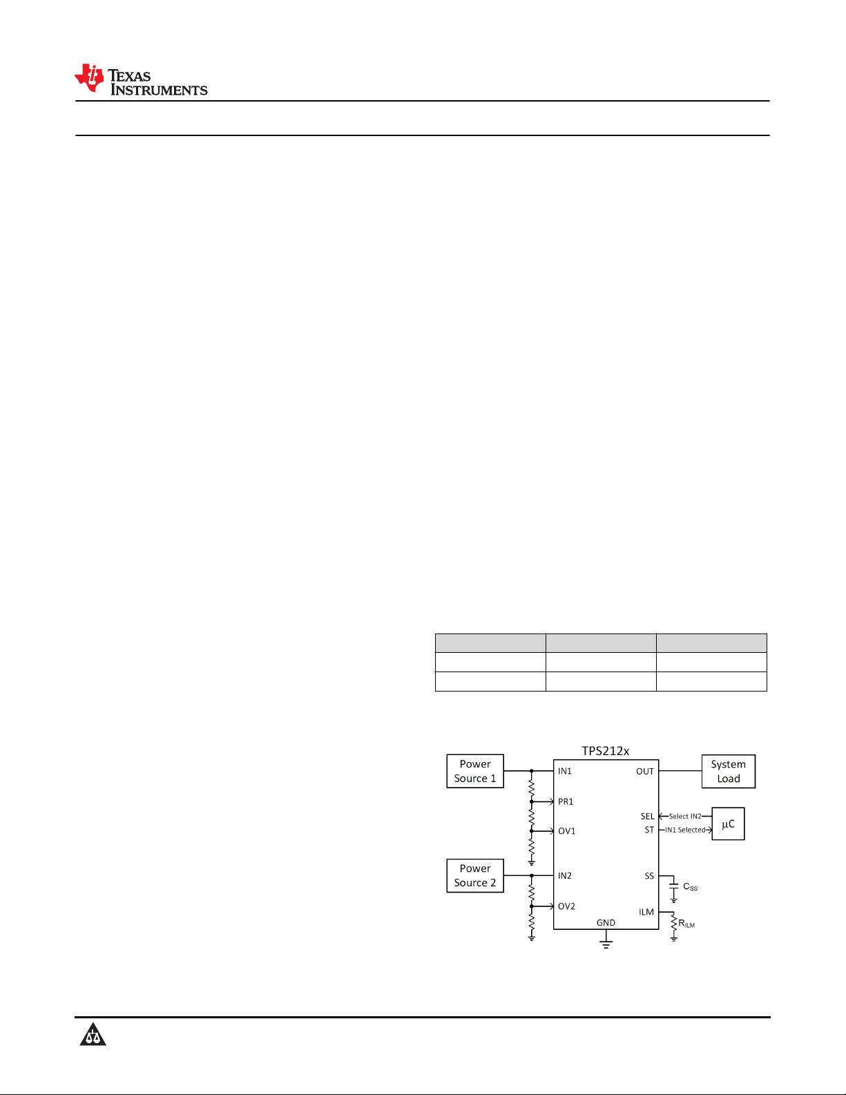
3 Description
The TPS212x devices are Dual-Input, Single-Output
(DISO) Power Multiplexer (MUX) that are well suited
for a variety of systems having multiple power
sources. The devices will Automatically Detect,
Select, and Seamlessly Transition between available
inputs.
Priority can be automatically given to the highest
input voltage or manually assigned to a lower voltage
input to support both ORing and Source Selection
operations. A priority voltage supervisor is used to
select an input source.
An Ideal Diode operation is used to seamlessly
transition between input sources. During switchover,
the voltage drop is controlled to block reverse current
before it happens and provide uninterrupted power to
the load with minimal hold-up capacitance.
Current limiting is used during startup and switchover
to protect against overcurrent events, and also
protects the device during normal operation. The
output current limit can be adjusted with a single
external resistor.
The TPS212x devices are available in WCSP and
small VQFN-HR package options characterized for
operation for a temperature range of –40°C to 125°C.
Device Information
PART NUMBER PACKAGE
TPS2120 WCSP (20) 1.5 mm x 2.0 mm
TPS2121 VQFN-HR (12) 2.0 mm x 2.5 mm
(1) For all available packages, see the orderable addendum at
the end of the data sheet.
(1)
BODY SIZE (NOM)
Typical Application
An IMPORTANT NOTICE at the end of this data sheet addresses availability, warranty, changes, use in safety-critical applications,
Copyright © 2020 Texas Instruments Incorporated
intellectual property matters and other important disclaimers. PRODUCTION DATA.
Product Folder Links: TPS2120 TPS2121
Submit Document Feedback
1

TPS2120, TPS2121
SLVSEA3F – AUGUST 2018 – REVISED AUGUST 2020
www.ti.com
Table of Contents
1 Features............................................................................1
2 Applications..................................................................... 1
3 Description.......................................................................1
4 Revision History.............................................................. 2
5 Device Comparison Table...............................................3
6 Pin Configuration and Functions...................................4
7 Specifications.................................................................. 6
7.1 Absolute Maximum Ratings........................................ 6
7.2 ESD Ratings............................................................... 6
7.3 Recommended Operating Conditions.........................6
7.4 Thermal Information....................................................6
7.5 Electrical Characteristics.............................................7
7.6 Typical Characteristics................................................9
8 Parameter Measurement Information.......................... 10
9 Detailed Description...................................................... 11
9.1 Overview................................................................... 11
9.2 Functional Block Diagram......................................... 11
9.3 Feature Description...................................................12
9.4 TPS2120 Device Functional Modes..........................18
9.5 TPS2121 Device Functional Modes..........................18
10 Application and Implementation................................ 19
10.1 Application Information........................................... 19
10.2 Typical Application.................................................. 19
10.3 Automatic Switchover with Priority (XCOMP)......... 25
10.4 Automatic Seamless Switchover with Priority
(XREF)........................................................................ 27
10.5 Highest Voltage Operation (VCOMP)..................... 28
10.6 Reverse Polarity Protection with TPS212x............. 31
10.7 Hotplugging with TPS212x......................................31
11 Power Supply Recommendations..............................33
12 Layout...........................................................................33
12.1 Layout Guidelines................................................... 33
12.2 Layout Example...................................................... 33
13 Device and Documentation Support..........................34
13.1 Documentation Support.......................................... 34
13.2 Receiving Notification of Documentation Updates..34
13.3 Support Resources................................................. 34
13.4 Trademarks.............................................................34
13.5 Electrostatic Discharge Caution..............................34
13.6 Glossary..................................................................34
14 Mechanical, Packaging, and Orderable
Information.................................................................... 34
4 Revision History
NOTE: Page numbers for previous revisions may differ from page numbers in the current version.
Changes from Revision E (February 2020) to Revision F (August 2020) Page
• Updated the numbering format for tables, figures and cross-references throughout the document ..................1
Changes from Revision D (September 2019) to Revision E (February 2020) Page
• Updated the Leakage Current in the Electrical Characteristics table in the Specifications section.................... 6
Changes from Revision C (February 2019) to Revision D (September 2019) Page
• Updated the Reverse Polarity Protection with TPS212x section ..................................................................... 31
• Updated the Hotplugging with TPS212x section ............................................................................................. 31
Changes from Revision B (December 2018) to Revision C (February 2019) Page
• Changed the Adjustable Overvoltage Supervisor (OVx) Accuracy to < ±5% in the Features section................ 1
• Changes made in the Recommended Operating Conditions and Electrical Characteristics table in the
Specifications section......................................................................................................................................... 6
• Changes made in the Active Current Limiting (ILM) section.............................................................................13
• Changed (typical) from 170°C to 160°C in the Thermal Protection (TSD) section............................................ 14
• Changed Equation 8 and Equation 9 ...............................................................................................................23
Changes from Revision A (November 2018) to Revision B (December 2018) Page
• Changed from Advance Information to Production Data.................................................................................... 1
Changes from Revision * (August 2018) to Revision A (November 2018) Page
• Changed Wide Operating Range to 2.7 V to 22 V..............................................................................................1
• Revised the Application and Implementation section....................................................................................... 19
2 Submit Document Feedback
Copyright © 2020 Texas Instruments Incorporated
Product Folder Links: TPS2120 TPS2121

www.ti.com
SLVSEA3F – AUGUST 2018 – REVISED AUGUST 2020
5 Device Comparison Table
Part Number Package On-Resistance Maximum Current Fastest Switchover Unique Pin
TPS2120 WCSP (20) 62 mΩ 3 A 100 us SEL
TPS2121 VQFN-HR (12) 56 mΩ 4.5 A 5 us CP2
TPS2120, TPS2121
Copyright © 2020 Texas Instruments Incorporated
Product Folder Links: TPS2120 TPS2121
Submit Document Feedback
3
TPS2120, TPS2121
SLVSEA3F – AUGUST 2018 – REVISED AUGUST 2020
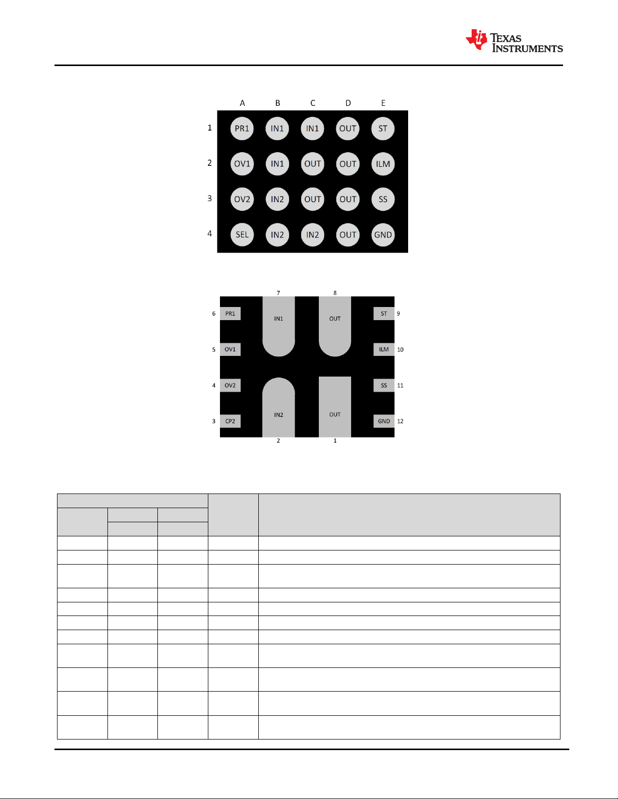
6 Pin Configuration and Functions
Figure 6-1. TPS2120 (YFP) Package 20-Pin WCSP Bottom View
www.ti.com
Figure 6-2. TPS2121 (RUX) Package 12-Pin VQFN-HR Bottom View
Pin Functions
PIN
NAME
IN1 B1, B2, C1 7 I Power Input for Source 1
IN2 B3, B4, C4 2 I Power Input for Source 2
OUT
ST E1 9 O Status output indicating which channel is selected. Connect to GND if not required.
ILIM E2 10 O Output Current Limiting for both channels.
SS E3 11 O Adjusts Input Setting Delay Time and Output Soft Start Time
GND E4 12 — Device Ground
PR1 A1
OV1 A2
OV2 A3
SEL A4
TPS2120 TPS2121
WCSP VQFN-HR
C2, C3, D1,
D2, D3, D4
1, 8
6
5
4
—
I/O DESCRIPTION
I Power Output
Enables Priority Operation. Connect to IN1 to set switchover voltage. Connect to
I
GND if not required.
Active Low Enable Supervisor for IN1 Overvoltage Protection. Connect to GND if
I
not required.
Active Low Enable Supervisor for IN2 Overvoltage Protection. Connect to GND if
I
not required.
Active low Enable for IN1. Allows GPIO to override priority operation and manually
I
select IN2. TPS2120 only.
4 Submit Document Feedback
Copyright © 2020 Texas Instruments Incorporated
Product Folder Links: TPS2120 TPS2121

www.ti.com
NAME
CP2 —
TPS2120 TPS2121
PIN
WCSP VQFN-HR
3
SLVSEA3F – AUGUST 2018 – REVISED AUGUST 2020
Pin Functions (continued)
I/O DESCRIPTION
Enables Comparator Operation and is compared to PR1 to set switchover voltage.
I
Connect to GND if not required. TPS2121 only.
TPS2120, TPS2121
Copyright © 2020 Texas Instruments Incorporated
Product Folder Links: TPS2120 TPS2121
Submit Document Feedback
5
TPS2120, TPS2121
SLVSEA3F – AUGUST 2018 – REVISED AUGUST 2020
www.ti.com
7 Specifications
7.1 Absolute Maximum Ratings
over operating free-air temperature range (unless otherwise noted)
V
, V
,
, V
,
IN2
Maximum Power Pin Voltage
Maximum Overvoltage Pin Voltage OV1, OV2 -0.3 6 V
Maximum Control Pin Voltage PRI, SEL -0.3 6 V
SEL
Maximum Control Pin Voltage ST -0.3 6 V
Maximum Output Current OUT Internally Limited
Maximum Junction Temperature Internally Limited
Storage temperature -65 150 °C
IN1
V
OUT
V
OV1
V
OV2
V
PRI
V
ST
I
OUT
T
J, MAX
T
STG
(1) Stresses beyond those listed under Absolute Maximum Rating may cause permanent damage to the device. These are stress ratings
only, which do not imply functional operation of the device at these or any other conditions beyond those indicated under
Recommended Operating Condition. Exposure to absolute-maximum-rated conditions for extended periods may affect device
reliability.
7.2 ESD Ratings
Human body model (HBM), per ANSI/ESDA/
V
ESD
Electrostatic discharge
JEDEC JS-001,
Charged device model (CDM), per JEDEC
specification JESD22-C101,
(1)
(1)
Pins MIN MAX UNIT
IN1, IN2,
OUT
-0.3 24 V
Pins VALUE UNIT
All ±2000
(2)
All ±500
V
(1) JEDEC document JEP155 states that 500-V HBM allows safe manufacturing with a standard ESD control process.
(2) JEDEC document JEP157 states that 250-V CDM allows safe manufacturing with a standard ESD control process.
7.3 Recommended Operating Conditions
over operating free-air temperature range (unless otherwise noted)
Pins MIN MAX UNIT
V
, V
IN1
V
OUT
V
OV1
V
OV2
V
, V
PRI
V
ST
R
ST
R
ILM
V
SS
I
, I
IN1
I
, I
IN1
T
J
Input Voltage Range
IN2
Output Voltage Range OUT 0 22 V
,
Overvoltage Pin Voltage OV1, OV2 0 5.5 V
Control Pin Voltage PRI, SEL 0 5.5 V
SEL
Control Pin Voltage ST 0 5.5 V
Status Pin Pull Up Resistance ST 6 20 kΩ
Current Limit Resistance ILM 18 100 kΩ
SS Pin Output Voltage SS 4 V
TPS2120 Continuous Input Current IN1, IN2 3 A
IN2
TPS2121 Continuous Input Current IN1, IN2 4.5 A
IN2
Junction temperature - -40 125 °C
(1) See Power Supply Recommendations Section for more Details
7.4 Thermal Information
THERMAL METRIC
R
θJA
Junction-to-ambient thermal resistance 72.5 72.2 °C/W
(1)
IN1, IN2 2.8 22 V
TPS2120 TPS2121
(1)
20 PINS 11 PINS
UNITYFP (WCSP) RNW (PKG FAM)
6 Submit Document Feedback
Copyright © 2020 Texas Instruments Incorporated
Product Folder Links: TPS2120 TPS2121
www.ti.com
SLVSEA3F – AUGUST 2018 – REVISED AUGUST 2020
7.4 Thermal Information (continued)
TPS2120, TPS2121
TPS2120 TPS2121
THERMAL METRIC
(1)
UNITYFP (WCSP) RNW (PKG FAM)
20 PINS 11 PINS
R
θJC(top)
R
θJB
Ψ
JT
Ψ
JB
R
θJC(bot)
Junction-to-case (top) thermal resistance 0.5 38.5 °C/W
Junction-to-board thermal resistance 16.4 15.4 °C/W
Junction-to-top characterization parameter 0.3 0.9 °C/W
Junction-to-board characterization parameter 16.6 15.5 °C/W
Junction-to-case (bottom) thermal resistance N/A N/A °C/W
(1) For more information about traditional and new thermal metrics, see the Semiconductor and IC Package Thermal Metrics application
report.
7.5 Electrical Characteristics
over operating free-air temperature range (unless otherwise noted)
PARAMETER TEST CONDITIONS T
INPUT SOURCE (IN1, IN2)
I
Q, INx
I
SBY, INx
I
LK, INx
V
Quiescent Current
(INx Powering OUT)
Standby Current
(INx not powering OUT)
Leakage Current
(INx to OUT)
Undervoltage Lockout
UV, INx
OUTPUT SWITCHOVER (OUT)
t
SW
t
FSW
V
Switchover Time
Fast Switchover Time
(TPS2121 only)
Input Voltage Comparator
COMP
(V
referenced to V
IN2
ON-RESISTANCE (INx to OUT)
ON-State Resistance (TPS2120)
R
ON
ON-State Resistance (TPS2121)
CURRENT LIMIT (ILM)
(1)
IN1
J
OUT = Open -40°C to 125°C 300 400 µA
V
= V
INx
(1)
OUT
25°C 0 15 25 µA
-40°C to 125°C 25 µA
25°C -1 1 µA
|V
- V
INx
OUT
| ≤ 5V
-40°C to 85°C -5 5 µA
-40°C to 125°C -80 80 µA
25°C -1 1 µA
|V
- V
INx
OUT
| ≤ 22V
-40°C to 85°C -35 35 µA
-40°C to 125°C -500 500 µA
V
Rising -40°C to 125°C 2.5 2.65 2.8 V
INx
V
Falling -40°C to 125°C 2.4 2.55 2.7 V
INx
V
< V
OUT
OUT
IN1
IN1
INx
REF
< V
INx
REF
≥ V
IN2
> V
, Falling Hysteresis -40°C to 125°C 2.5 3.5 4.5 %
IN2
CP2 or SEL < V
V
CP2 ≥ V
V
)
V
-40°C to 125°C 100 µs
-40°C to 125°C 5 µs
-40°C to 125°C 0 280 600 mV
25°C 62 75 mΩ
I
= -200 mA
OUT
V
V
PRI
INx
> V
REF
≥ 5.0 V
-40°C to 85°C 90 mΩ
-40°C to 105°C 100 mΩ
-40°C to 125°C 120 mΩ
25°C 56 70 mΩ
I
= -200 mA
OUT
V
V
PRI
INx
> V
REF
≥ 5.0 V
-40°C to 85°C 85 mΩ
-40°C to 105°C 90 mΩ
-40°C to 125°C 100 mΩ
MIN TYP MAX UNIT
Copyright © 2020 Texas Instruments Incorporated
Product Folder Links: TPS2120 TPS2121
Submit Document Feedback
7
TPS2120, TPS2121
SLVSEA3F – AUGUST 2018 – REVISED AUGUST 2020
7.5 Electrical Characteristics (continued)
over operating free-air temperature range (unless otherwise noted)
PARAMETER TEST CONDITIONS T
R
= 31.6kΩ -40°C to 125°C 3 3.5 4 A
ILM
R
= 46.4kΩ -40°C to 125°C 2 2.5 3 A
Output Current Limit (TPS2120)
(2)
I
LM
Output Current Limit (TPS2121)
(3)
t
LM
Current Limit Response Time Output Steady State -40°C to 125°C 250 µs
CONTROL PINS (PRI, SEL, OV1, OV2)
V
V
I
LK, x
Internal Voltage Reference
REF, x
Comparator Offset Voltage
OFST
(TPS2121 only)
Pin Leakage Current
STATUS INDICATION PIN (ST)
I
LK, ST
t
ST
Pin Leakage VST = 0 V to 5.5 V -40°C to 125°C -0.1 0.1 µA
Status Delay L to H -40°C to 125°C 1 µs
FAST REVERSE CURRENT BLOCKING (RCB)
I
RCB
V
t
RCB
Fast Reverse Current Detection
Threshold
RCB Release Voltage V
RCB
Fast Reverse Current Blocking
Response Time
THERMAL SHUTDOWN (TSD)
T
Thermal Shutdown
SD
ILM
R
= 85kΩ -40°C to 125°C 1 1.5 2 A
ILM
R
< 1kΩ -40°C to 125°C 1.5 2.5 3.5 A
ILM
R
= 18.7kΩ -40°C to 125°C 4.6 5.2 5.8 A
ILM
R
= 22.1kΩ -40°C to 125°C 4 4.5 5 A
ILM
R
= 29.8kΩ -40°C to 125°C 3 3.5 4 A
ILM
R
= 44.2kΩ -40°C to 125°C 2 2.5 3 A
ILM
R
= 80kΩ -40°C to 125°C 1 1.5 2 A
ILM
R
< 1kΩ -40°C to 125°C 1.5 2.5 3.5 A
ILM
V
, V
PR1
CP2, VOV1
V
, V
PR1
CP2, VOV1
V
> V
PR1
V
> V
CP2
V
, V
PR1
CP2, VOV1
REF
REF
, V
Rising -40°C to 125°C 1.01 1.06 1.1 V
OV2
, V
Falling -40°C to 125°C 0.99 1.04 1.09 V
OV2
, V
= 0 V to 5.5
OV2
V
V
> V
OUT
INx
> V
OUT
INx
Shutdown Rising 160 °C
Recovery Falling 150 °C
www.ti.com
J
MIN TYP MAX UNIT
-40°C to 125°C 5 20 40 mV
-40°C to 125°C -0.1 0.1 µA
-40°C to 125°C 0.2 1 2 A
-40°C to 125°C 0 25 50 mV
-40°C to 125°C 10 µs
(1) When PR1 < V
not to exceed I
, CP2 < V
REF
Q,INx
, and |V
.
REF
| < 1V, Quiescent current can be drawn from both IN1 and IN2 with combined current
IN1-VIN2
(2) The current limit can be measured by forcing a voltage differential from VIN to VOUT. This value must be at least 200mV greater than
the voltage drop across the device at the current limit threshold (ILM x R
voltage drop of (1.5A x 100mΩ + 200mV) = 350mV from VIN to VOUT for a current limit setting of 1.5A (typical).
). For example, the TPS2121 would need a minimum
ON(MAX)
(3) For more information on device behavior during short circuit conditions, see Section 9.3.3.
8 Submit Document Feedback
Copyright © 2020 Texas Instruments Incorporated
Product Folder Links: TPS2120 TPS2121
Input Voltage (V)
Quiescent Current (PA)
2 4 6 8 10 12 14 16 18 20 22
240
248
256
264
272
280
288
296
304
312
320
D001
-40qC
25qC
85qC
125qC
Input Voltage (V)
Quiescent Current (PA)
2 4 6 8 10 12 14 16 18 20 22
160
180
200
220
240
260
D002
-40qC
25qC
85qC
125qC
Input Voltage (V)
Standby Current (PA)
2 4 6 8 10 12 14 16 18 20 22
6
7
8
9
10
11
12
13
14
15
16
D003
-40qC
25qC
85qC
125qC
Input Voltage (V)
Standby Current (PA)
2 4 6 8 10 12 14 16 18 20 22
6
8
10
12
14
16
18
D004
-40qC
25qC
85qC
125qC
Input Voltage (V)
On-Resistance (m:)
2 4 6 8 10 12 14 16 18 20 22
40
48
56
64
72
80
88
96
104
D005
-40qC
25qC
85qC
125qC
CSS Capacitor (nF)
Output Slew Rate (V/ms)
1 2 3 4 5 67 10 20 30 50 70100 200 500 1000
0
3
6
9
12
15
18
D006
5V
12V
20V
www.ti.com
7.6 Typical Characteristics
SLVSEA3F – AUGUST 2018 – REVISED AUGUST 2020
TPS2120, TPS2121
ILM = 5.2A
Figure 7-1. Quiescent Current vs Input Voltage
ILM = 5.2A
Figure 7-3. Standby Current vs Input Voltage
ILM = 1.5A
Figure 7-2. Quiescent Current vs Input Voltage
ILM = 1.5A
Figure 7-4. Standby Current vs Input Voltage
I
= -200 mA
OUT
Figure 7-5. TPS2121 On-Resistance vs Input
Voltage
Copyright © 2020 Texas Instruments Incorporated
V
> UVLO V
IN1
Figure 7-6. Output Slew Rate vs CSS Capacitor
Product Folder Links: TPS2120 TPS2121
= 0V
IN2
Submit Document Feedback
9
TPS2120, TPS2121
SLVSEA3F – AUGUST 2018 – REVISED AUGUST 2020
V
= 12 V V
IN1
IN2
= 0 V
Figure 7-7. TPS2121 Hot Short on OUT while IN1 is
Enabled
8 Parameter Measurement Information
www.ti.com
V
= 12 V V
IN1
R
= 71.5kΩ
ILM
= 0 V V
IN2
OUT
= GND
Figure 7-8. TPS2120 IN1 is Enabled with a Short on
OUT
10 Submit Document Feedback
Figure 8-1. Timing Parameter Diagram
Copyright © 2020 Texas Instruments Incorporated
Product Folder Links: TPS2120 TPS2121
+
±
V
REF
Control Logic
+ Gate Drivers
+
±
+
±
+
±
Temp
SNS
Current
Limit
V
REF
V
REF
V
REF
Temp
SNS
BFET1 HFET1
BFET2 HFET2
IN1
PR1
SEL
OV1
OV2
IN2
ST
GND
SS
OUT
ILM
www.ti.com
SLVSEA3F – AUGUST 2018 – REVISED AUGUST 2020
9 Detailed Description
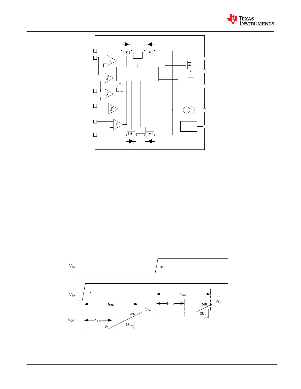
9.1 Overview
The TPS212x devices are Dual-Input, Single-Output (DISO) Power Multiplexer (MUX) that are well suited for a
variety of systems having multiple power sources. The devices will automatically detect, select, and seamlessly
transition between available inputs. Priority can be automatically given to the highest input voltage or manually
assigned to a lower voltage input to support both ORing and Source Selection operations. A priority voltage
supervisor is used to select an input source.
An Ideal Diode operation is used to seamlessly transition between input sources. During switchover, the voltage
drop is controlled to block reverse current before it happens and provide uninterrupted power to the load with
minimal hold-up capacitance. Active current limiting is used during startup and switchover to protect against
overcurrent, and also protects the device during normal operation. The output current limit can be adjusted with
a single external resistor.
9.2 Functional Block Diagram
The below figures show the block diagrams for the TPS2120 and TPS2121. The TPS2120 has the SEL pin,
while the TPS2121 has the CP2 pin and supports fast switchover.
TPS2120, TPS2121
Figure 9-1. TPS2120 Functional Block Diagram
Copyright © 2020 Texas Instruments Incorporated
Product Folder Links: TPS2120 TPS2121
Submit Document Feedback
11
+
±
V
REF
Control Logic
+ Gate Drivers
+
±
+
±
+
±
Temp
SNS
Current
Limit
V
REF
V
REF
V
REF
Temp
SNS
BFET1 HFET1
BFET2 HFET2
IN1
PR1
CP2
OV1
OV2
IN2
ST
GND
SS
OUT
ILM
+
±
V
OFST
TPS2120, TPS2121
SLVSEA3F – AUGUST 2018 – REVISED AUGUST 2020
Figure 9-2. TPS2121 Functional Block Diagram
www.ti.com
9.3 Feature Description
This section describes the different features of the TPS212x power mux device.
9.3.1 Input Settling Time and Output Soft Start Control (SS)
The TPS212x will automatically select the first source to become valid (INx >UV and INx <OV). The external
capacitor (CSS) will then be used as a timer to wait for the input to finish setting (tSETx). When the settling timer
has expired, CSS will continue to charge and set the output slew rate (SRON) for a soft start. After the total turn
on time (tONx), soft start will not be used again for INx until it ceases to be valid (INx <UV or INx >OV).
When the second source becomes valid (INy >UV and INy <OV), the external capacitor (Css) will be used again
for a second settling time (tSETy). After tSETy, the TPS212x will decide whether to continue sourcing the first
source, or switchover to the second source. If the second source is selected at the end of tSETy, then CSS will
be reused to set the output slew rate (SRON) for a second soft start. After the total turn on time (tONy), soft start
will not be used again for INy until it ceases to be valid (INy <UV or INy >OV).
If INy becomes valid before the end of tONx, tSETy will be delayed and start after tONx has ended.
12 Submit Document Feedback
Figure 9-3. Settling and Soft Start Timing
Product Folder Links: TPS2120 TPS2121
Copyright © 2020 Texas Instruments Incorporated
LM
0.861
ILM
69.1
IR
LM
0.861
ILM
65.2
IR
www.ti.com
SLVSEA3F – AUGUST 2018 – REVISED AUGUST 2020
If INy is not selected during tSETy, a second soft start will not take place, skipping tONy, and CSS will be retired
until one of the inputs ceases to be valid.
9.3.1.1 Slew Rate vs. CSS Capacitor
Table 9-1 shows the estimated slew rate across CSS capacitance and VIN.
Table 9-1. Slew Rate vs. CSS Capacitor
TPS2120, TPS2121
CSS CAPACITOR VIN = 5 V VIN = 12 V VIN = 20 V UNITS
100 nF 780 800 880 V/s
1 uF 88 92 92 V/s
10 uF 8.8 9.6 10.4 V/s
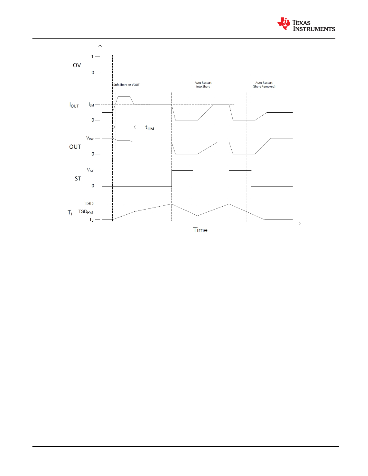
9.3.2 Active Current Limiting (ILM)
The load current is monitored at all times. When the load current exceed the current limit trip point ILM
programmed by RILM resistor, the device regulates the current within t
. The following equations can be used
ILM
to find the RILM value for a desired current limit, where RILM is in kΩ and between 18 kΩ to 100 kΩ.
TPS2120:
TPS2121:
(1)
(2)
During current regulation, the output voltage will drop resulting in increased device power dissipation. If the
device junction temperature (TJ) reaches the thermal shutdown threshold (TSD) the internal FETs are turned off.
After cooling down, the device will automatically restart.
Copyright © 2020 Texas Instruments Incorporated
Product Folder Links: TPS2120 TPS2121
Submit Document Feedback
13
TPS2120, TPS2121
SLVSEA3F – AUGUST 2018 – REVISED AUGUST 2020
www.ti.com
Figure 9-4. Current Limiting Behavior
9.3.3 Short-Circuit Protection
During a transient short circuit event, the current through the device increases very rapidly. As the current-limit
amplifier cannot respond quickly to this event due to its limited bandwidth, the device incorporates a fast-trip
overcurrent protection (OCP) comparator, with a threshold I
within 1 µs, when the current through internal FET IOUT exceeds I
about 2.4x of the programmed current limit I
= 2.4 × ILM. The OCP circuit holds the internal FET off for about
OCP
. This comparator shuts down the pass device
OCP
(I
> I
OCP
OUT
). The trip threshold is set to
OCP
25 ms, after which the device turns back on. If the short is still present then the current-limit loop will regulate the
output current to ILM and behave in a manner similar to a power up into a short.
9.3.4 Thermal Protection (TSD)
The TPS212x devices have built-in absolute thermal shutdown and relative thermal shutdown to ensure
maximum reliability of the power mux. The absolute thermal shutdown is designed to disable the power FETs, if
the junction temperature exceeds 160°C (typical). The device auto recovers about 25 ms after TJ < [T (TSD) –
10°C]. The relative thermal shutdown protects the device by turning off when the temperature of the power FETs
increases sharply such that the FET temperature rises about 60°C above the rest of the die. The device auto
recovers about 25 ms after the FETs cools down by 20°C. The relative thermal shutdown is critical for protecting
the device against faults such as a power up into a short which causes the FET temperature to increase sharply.
9.3.5 Overvoltage Protection (OVx)
Output Overvoltage Protection is available for both IN1 and IN2 in case either applied voltage is greater than the
maximum supported load voltage. The VREF comparator on the OVx pins allow for the Overvoltage Protection
threshold to be adjusted independently for each input. When overvoltage is engaged, the corresponding channel
will turn off immediately. Fast switchover to the other input is supported if it is a valid voltage.
14 Submit Document Feedback
Copyright © 2020 Texas Instruments Incorporated
Product Folder Links: TPS2120 TPS2121

V
SUP PLY
R1
R2
OVx
OUT,MIN SW DIP
V = V - V
OUT
DIP SW
OUT
I
V t
C
§ ·
u
¨ ¸
¨ ¸
© ¹
www.ti.com
SLVSEA3F – AUGUST 2018 – REVISED AUGUST 2020
TPS2120, TPS2121
Figure 9-5. OVP Resistor Configuration
9.3.6 Fast Reverse Current Blocking (RCB)
Each channel has the always on reverse current blocking. If the output is forced above the selected input by
V
, the channel will switch off to stop the reverse current I
IRCB
RCB
within t
. As the output falls to within V
RCB
VIN, the selected channel will quickly turn back on to avoid unnecessary voltage drops during fast switchover
(tSW).
RCB
of
9.3.7 Output Voltage Dip and Fast Switchover Control (TPS2121 only)
After input settling and soft start time, the TPS2121 utilizes a fast switchover to minimize output voltage drop.
Where VSW is the output voltage when the switchover is triggered and tSW is the time until the output voltage
stops dipping. The amount of voltage dip during the switchover time is a function of output load current (IOUT)
and load capacitance (COUT). The minimum output voltage during switchover can be found using the following
equations:
Where:
Copyright © 2020 Texas Instruments Incorporated
Figure 9-6. Reverse Current Blocking Behavior
Product Folder Links: TPS2120 TPS2121
(3)
(4)
Submit Document Feedback
15

V
IN1
I
OUT
V
IN2
V
IN2
V
IN1
0 V
V
SW
t
SW
V
OUT,MIN
Current Limited
0
V
OUT
I
IN2
SR
OUT
Input
Voltages
PRI
V
OUT,MIN
= V
SW
- (tSWxSR
OUT
) where SR
OUT
= I
OUT/COUT
V
OUT,MIN
= 3.5 V - (5µs x 30mV/µs) = 3.35 V
V
OUT,MIN
= 3.5 V - (5µs x 1A/10µF) = 3 V
V
OUT,MIN
= 3.5 V - (5µs x 1A/100µF) = 3.45 V
Time
V
REF
H
L
TPS2120, TPS2121
SLVSEA3F – AUGUST 2018 – REVISED AUGUST 2020
www.ti.com
Figure 9-7. Minimum Output Voltage During Fast Switchover
If switching from a lower to a higher voltage, the selected channel will not detect reverse voltage and shall turn
on immediately using the current monitor to limit the output current to a safe level. If the output current reaches
the current limit during fast switchover, this will increase the total time until the output reaches steady state.
Figure 9-8. Fast Switchover from Lower to Higher Voltage
If an input is selected while the output voltage is still a higher voltage, that channel will continue to block reverse
current by waiting to fast turn on until the output drops below the V
16 Submit Document Feedback
Product Folder Links: TPS2120 TPS2121
threshold.
RCB
Copyright © 2020 Texas Instruments Incorporated

V
OUT,MIN
= V
IN1
+ V
RCB
- (t
SW
x SR
OUT
) where SR
OUT
= I
OUT/COUT
V
OUT,MIN
= 4.25 V + 50 mV - (5µs x 30mV/µs) = 4.15 V
V
OUT,MIN
= 4.25 V + 50 mV - (5µs x 1A/10µF) = 3.8 V
V
OUT,MIN
= 4.25 V + 50 mV (5µs x 1A/100µF) = 4.25 V
SR
OUT
V
RCB
t
SW
V
OUT,MIN
No Spikes
Input
Voltages
OV2
V
OUT
I
IN1
Time
V
IN1
I
OUT
V
IN2
V
IN2
V
IN1
0 V
0
1
0
www.ti.com
SLVSEA3F – AUGUST 2018 – REVISED AUGUST 2020
TPS2120, TPS2121
Figure 9-9. Fast Switchover from Higher to Lower Voltage
9.3.8 Input Voltage Comparator (VCOMP)
If both PR1 and CP2 are < VREF, the device will use an internal comparator between the two inputs to
determine the priority source. V
If IN2 falls below the V
Hysteresis, then IN1 will have priority.
COMP
is configured to ensure IN2 will take priority if the input voltages are equal.
COMP
Figure 9-10. VCOMP Priority Source Selection
Copyright © 2020 Texas Instruments Incorporated
Product Folder Links: TPS2120 TPS2121
Submit Document Feedback
17

TPS2120, TPS2121
SLVSEA3F – AUGUST 2018 – REVISED AUGUST 2020
9.4 TPS2120 Device Functional Modes
Table 9-2 shows the TPS2120 functional behavior.
Table 9-2. TPS2120 Output Source Selection Table
DEVICE INPUTS DEVICE OUTPUTS
IN1 ≤ UV OR
OV1 ≥ VREF OR
SEL ≥VREF
0 0 0 IN2 < IN1 IN1 H VCOMP
0 0 0 IN2 ≥ IN1 IN2 L VCOMP
0 0 1 X IN1 H VREF
0 1 X X IN1 H Invalid Input
1 0 X X IN2 L SEL / Invalid Input
1 1 X X Hi-Z H Invalid Inputs
IN2 ≤ UV OR
OV2 ≥ VREF
PR1 ≥ VREF VCOMP OUT ST MODE
A summary of the operation of the TPS2120 device can be found below:
• If only one input voltage is valid (above UV and below OV) then that input will power the output.
• If both inputs are not valid, then the output is Hi-Z.
• ST is pulled high when the output is Hi-Z or IN1. It is pulled low when IN2 is powering the output.
• If both inputs are valid and PR1 is pulled high (higher than VREF, 1.06-V typical), then IN1 is used.
• If both inputs are valid and PR1 is pulled low, then the highest voltage input is used.
OPERATION
www.ti.com
MODE OF
9.5 TPS2121 Device Functional Modes
Table 9-3 shows the TPS2121 functional behavior.
Table 9-3. TPS2121 Output Source Selection Table
DEVICE INPUTS DEVICE OUTPUTS
IN1 ≤ UV OR
OV1 ≥ VREF
0 X 0 0 IN2 < IN1 X IN1 H VCOMP
X 0 0 0 IN2 ≥ IN1 X IN2 L VCOMP
0 X 0 1 X X IN1 H VREF
X 0 1 0 X X IN2 L VREF
0 X 1 1 X PR1 > CP2 IN1 H XCOMP / XREF
X 0 1 1 X PR1 ≤ CP2 IN2 L XCOMP / XREF
0 1 X X X X IN1 H Invalid Input
1 0 X X X X IN2 L Invalid Input
1 1 X X X X Hi-Z H Invalid Inputs
IN2 ≤ UV OR
OV2 ≥ VREF
CP2 ≥
VREF
PR1 ≥
VREF
VCOMP XCOMP OUT ST MODE
A summary of the operation of the TPS2121 device can be found below:
• If only one input voltage is valid (above UV and below OV) then that input will power the output.
• If both inputs are not valid, then the output is Hi-Z.
• ST is pulled high when the output is Hi-Z or IN1. It is pulled low when IN2 is powering the output.
• If CP2 is pulled low, then the TPS2121 ignores this pin.
• When CP2 is pulled high, this enables fast switchover and is compared to PR1. If PR1 > CP2 then IN1 is
used, and if PR1 < CP2 then IN2 is used.
• If both inputs are valid, CP2 is low, and PR1 is pulled high, (higher than VREF, 1.06-V typical), then IN1 is
used.
• If both inputs are valid, CP2 is low, and PR1 is pulled low, then the highest voltage input is used.
MODE OF
OPERATION
18 Submit Document Feedback
Copyright © 2020 Texas Instruments Incorporated
Product Folder Links: TPS2120 TPS2121

www.ti.com
SLVSEA3F – AUGUST 2018 – REVISED AUGUST 2020
10 Application and Implementation
Note
Information in the following applications sections is not part of the TI component specification, and TI
does not warrant its accuracy or completeness. TI’s customers are responsible for determining
suitability of components for their purposes. Customers should validate and test their design
implementation to confirm system functionality.
10.1 Application Information
The TPS212x device is a highly configurable power mux that can be designed to meet various application
requirements. When designing the TPS212x for a power mux configuration, 3 key factors should be considered:
• VOUT voltage dip
• Manual and Automatic Switchover
• Switchover Time
The TPS212x device can be configured in various modes to meet these considerations and provides a general
table that describes each mode of operation. This application section will highlight 3 common modes of
operation that address these factors.
10.2 Typical Application
Table 10-1 summarizes the applications highlighted in the following sections.
TPS2120, TPS2121
Table 10-1. TPS212x Application Summary Table
MODE DEVICE(S) DESCRIPTION SECTION
Manual Switchover TPS2120 / TPS2121
Automatic Switchover with
Priority (XCOMP)
Automatic Switchover with
Priority (XREF)
Highest Voltage Operation
(VCOMP)
TPS2121
TPS2121
TPS2120 / TPS2121
An external controller (such as an MCU) can be used
to manually select between the two input sources.
Prioritizes Supply 1 when present, and quickly
switches to Supply 2 when Supply 1 drops.
Prioritizes Supply 1 when present, and quickly
switches to Supply 2 when Supply 1 drops. An external
supply is used to increase the accuracy of the
comparator for switchover.
The device automatically selects the highest voltage
supply to power the output.
11.2.1
11.3
11.4
11.5
Copyright © 2020 Texas Instruments Incorporated
Product Folder Links: TPS2120 TPS2121
Submit Document Feedback
19

TPS2120, TPS2121
SLVSEA3F – AUGUST 2018 – REVISED AUGUST 2020
10.2.1 Manual Switchover Schematic
Figure 10-1 and Figure 10-2 show the application schematic for manual switchover on the TPS2120 and
TPS2121.
www.ti.com
Figure 10-1. TPS2120 Manual Switchover
Figure 10-2. TPS2121 Manual Switchover
10.2.2 Design Requirements
In certain power architectures, an external MCU or controller monitors the downstream load. If the controller
needs to select between multiple supplies, the controller can manually switch between inputs through a single
GPIO. In this configuration, an external signal will switch between two input supplies, a 5-V supply (IN1) and a
3.3-V supply (IN2). Table 10-2 summarizes the design parameters for this example.
20 Submit Document Feedback
Copyright © 2020 Texas Instruments Incorporated
Product Folder Links: TPS2120 TPS2121

www.ti.com
SLVSEA3F – AUGUST 2018 – REVISED AUGUST 2020
Table 10-2. Manual Switchover Design Requirements
TPS2120, TPS2121
DESIGN PARAMETER SPECIFICATION DETAILS
IN1 Voltage V
IN2 Voltage V
Load Current I
Load Capacitance C
Maximum Inrush Current I
Current Limit 2 A
Switchover Time t
Mode of Operation Manual Switchover TPS2120: VREF
External MCU Signal V
Overvoltage Protection V
IN1
IN1
OUT
L
INRUSH
SW
MCU
OV1
V
OV2
5 V
3.3 V
500 mA
100 µF
100 mA
TPS2121: 5 µs
TPS2120: 100 µs
TPS2121: XREF
3.3 V
OV1 : 6.1 V
OV2: 4 V
10.2.3 Detailed Design Description
The TPS212x devices can be configured to manually switch between IN1 and IN2 through an external GPIO. In
this example, an external MCU signal is selecting between main power and auxiliary power to power a
downstream load. By manually toggling the TPS212x, the device will switch between both sources, even if one
supply is higher than the other supply. Ultimately, the main factor that will determine the switchover time between
IN1 (5 V) and IN2 (3.3 V) is the output load.
Manual switchover can be enabled by configuring the TPS212x for internal voltage reference control scheme
(VREF). In the VREF scheme, if the voltage on PR1 is higher than the internal VREF voltage, 1.06 V (typical),
the device will select IN1 as the output. If the voltage on PR1 drops below VREF, then the device will switch to
IN2, as long as IN2 is presenting a valid input voltage. IN1 is commonly connected to PR1 with an external
resistor divider. OV1 and OV2 can be configured to provide overvoltage protection. The ST pin can be pulled
high with a resistor to provide feedback on the status of the system. If the status pin is high, IN1 is the output. If
the pin is low, IN2 is the output. If this feature is not required, the ST pin can be connected to GND.
On the TPS2120, by connecting an external signal to the select pin (SEL), the device can override the PR1/
VREF comparison. If the voltage on SEL is higher than VREF at approximately (1.06 V), then the device will
select IN2, as shown on Table 9-2. If the voltage on SEL drops below VREF, then the device will switch to IN1 as
long as PR1 >= VREF. Otherwise, the highest voltage input will be chosen between IN1 and IN2. In this
example, since the IN1 is higher than IN2, at 5 V, it will be selected.
Copyright © 2020 Texas Instruments Incorporated
Product Folder Links: TPS2120 TPS2121
Submit Document Feedback
21

TPS2120, TPS2121
SLVSEA3F – AUGUST 2018 – REVISED AUGUST 2020
Figure 10-3 shows the application schematic for this design example on the TPS2120.
Figure 10-3. TPS2120 Manual Switchover
www.ti.com
On the TPS2121, fast switchover can be enabled to minimize the voltage drop on VOUT. The internal
comparator will detect and seamlessly switch between IN1 and IN2 as long as a reverse voltage condition does
not exist on that channel. To enable fast switchover on the TPS2121, CP2 needs to be higher than VREF, 1.06-V
(typical). By using the external voltage reference control scheme (XREF), the voltages on PR1 and CP2 pins are
compared to determine whether IN1 or IN2 is powering the output. If the voltage on PR1 is higher than CP2,
then IN1 is powering the output. If the voltage on PR1 is lower than CP2, then IN2 is powering the output.
Manual switchover on the TPS2121 is configured by connecting PR1 to IN1 with a resistor divider, and
connecting CP2 to the external 3.3-V MCU signal. If the voltage on CP2 is higher than the voltage on PR1, then
IN2 will power the output. However, if CP2 is toggled low, then IN1 will power the output, assuming IN1 has a
valid input voltage.
The diagram below shows the application schematic for this design example on the TPS2121.
22 Submit Document Feedback
Figure 10-4. TPS2121 Manual Switchover
Copyright © 2020 Texas Instruments Incorporated
Product Folder Links: TPS2120 TPS2121

PR1 IN1
5 k
V V
5 k 10.2 k
:
u
: :
IN1
5 k
5 k 10.2 k
:
u
: :
IN1
5 k
5 k 23.7 k
§ ·
:
u
¨ ¸
: :
© ¹
IN2
5 k
5 k 13.7 k
§ ·
:
u
¨ ¸
: :
© ¹
LM
0.861
69.1
I 2.06 A
59
www.ti.com
10.2.4 Design Procedure
10.2.4.1 Selecting PR1 and CP2 Resistors
The TPS2120 does not contain a CP2 pin. Instead, a select pin (SEL), enables override of the PR1 / VREF
comparison. Once the voltage on SEL is greater than VREF, the device will select IN2 as the output. For manual
switchover, an external signal can be connected to the SEL pin. For this example, the external MCU signal is a
3.3-V enable.
The TPS2121 can be configured for manual switchover in a similar manner as the TPS2120. Instead of a SEL
pin, the 3.3-V external MCU signal can be connected to CP2. As long as the voltage on CP2 is higher than PR1,
the device will select IN2 as the output. When the voltage on CP2 drops below PR1, the device will switch back
to IN1. Therefore, the resistor divider on PR1 is configured the same as above, with the 5 kΩ and 10.2 kΩ.
For additional precautions, the voltage on PR1 can also be configured. If the voltage on IN1 were to drop, the
device can automatically switchover to IN2. In this example, if voltage on IN1 drops below IN2 (3.3 V) then the
device will switch to IN2. Therefore, the resistor divider on PR1 should be configured such that the voltage on
PR1 will drop below VREF, when IN1 dips below 3.3 V. The bottom resistor is chosen to be 5 kΩ due to it's
commonality and minimal current leakage. If a smaller leakage is desired, a larger resistor can be used. With this
configuration, the top resistor was selected to be 10.2 kΩ. With this resistor configuration, the device will switch
to IN2 when the voltage on IN1 dips to 3.22 V. Refer to Table 9-2 for additional information regarding the
switchover configuration.
See Equation 5 for the VPR1 Calculation
SLVSEA3F – AUGUST 2018 – REVISED AUGUST 2020
TPS2120, TPS2121
(5)
10.2.4.2 Selecting OVx Resistors
Independent output overvoltage protection is available for both IN1 and IN2. The VREF comparator on the OV1
and OV2 pins allows for the overvoltage protection thresholds to be adjusted independently, allowing for different
overvoltage thresholds on each channel. When overvoltage is engaged, the corresponding channel will turn off
immediately if the pin reaches VREF, 1.06 V (typical). On this design, the overvoltage thresholds are triggered at
roughly 1-V higher than the nominal input voltages. On IN1, the overvoltage resistor divider was programmed to
be 6.08 V, where as the divider on IN2 was programmed to be 3.96 V. The OV resistor calculations are shown in
Equation 6 and Equation 7.
(6)
(7)
10.2.4.3 Selecting Soft-Start Capacitor and Current Limit Resistors
Equation 1 can be used to determine the RLIM values for this application. In this example, the DC load current is
1 A. Setting the current limit to 2 A will limit potential inrush current events and protect downstream loads. See
Equation 8 for the TPS2120 ILM Calculation:
Copyright © 2020 Texas Instruments Incorporated
Product Folder Links: TPS2120 TPS2121
(8)
Submit Document Feedback
23

LM
0.861
65.2
I 1.95 A
59
INRUSH
ON
I
SRC
ON
100 mA
SR 1000 V / S
100 F
P
TPS2120, TPS2121
SLVSEA3F – AUGUST 2018 – REVISED AUGUST 2020
www.ti.com
See Equation 9 for the TPS2121 ILM Calculation:
(9)
To calculate the slew rate needed to limit the inrush current to 100 mA, the Slew Rate Calculation can be used in
Equation 10:
(10)
(11)
Using this equation, the slew rate must be limited to 1000V/S or below to keep the inrush current below 100 mA.
According to Table 9-1, at 5 V a CSS capacitance of 100 nF will provide a slew rate of 780V/S (typical), which is
below the calculated threshold of 1000V/S. Therefore, a 100 nF capacitor will limit the inrush below 100 mA in a
typical application.
10.2.5 Application Curves
Figure 10-5. TPS2120 Switchover from IN1 to IN2 Figure 10-6. TPS2120 Switchover from IN2 to IN1
Figure 10-7. TPS2121 Switchover from IN1 to IN2 Figure 10-8. TPS2121 Switchover from IN2 to IN1
24 Submit Document Feedback
Copyright © 2020 Texas Instruments Incorporated
Product Folder Links: TPS2120 TPS2121

TPS2121
IN1
OUT
IN1
(12V)
PRI
System Load
(2A, 200µF)
OV1
GND
SS
ILM
ST
IN2
IN2
(5V)
5kO
63.4kO
5kO
18.2kO
21.5kO
1µF
5kO
10.2kO
5kO
CP2
OV2
23.7kO
www.ti.com
SLVSEA3F – AUGUST 2018 – REVISED AUGUST 2020
10.3 Automatic Switchover with Priority (XCOMP)
In certain applications, the system needs to provide uninterrupted sources of power. If one of the input power
supplies were to fail, the system needs to automatically switchover to a backup power source without interrupting
normal operation. In this example, two scenarios will be demonstrated. The first example will prioritize a 12-V
main supply, and switchover to a 5-V auxiliary supply whenever the 12 V is not present. The second example will
showcase power redundancy with two 12-V supplies. If one 12-V supply were to fail, the device will seamlessly
switchover to the backup supply.
10.3.1 Application Schematic
Figure 10-9 shows the application schematic for automatic switchover on the TPS2121 between a 12-V and 5-V
supply.
TPS2120, TPS2121
Figure 10-9. Automatic Switchover Between 12 V and 5 V
10.3.2 Design Requirements
Table 10-3. Automatic Switchover Design Requirements
DESIGN PARAMETER SPECIFICATION DETAILS
IN1 Voltage V
IN2 Voltage V
Load Current I
Load Capacitance C
Maximum Inrush Current I
Mode of Operation Automatic Switchover TPS2121: XCOMP
Switchover Time t
IN1
IN1
OUT
L
INRUSH
SW
12 V
5 V
2 A
200 µF
100 mA
TPS2120: 5 µs
10.3.3 Detailed Design Description
The first example demonstrates automatic switchover from main power (IN1) to standby power (IN2). This
architecture is commonly found on applications that require a secondary/auxiliary input to conserve power while
keeping downstream loads on. When switching between main and auxiliary power, the voltage drop on the
output should also be minimal to prevent the downstream load from resetting or entering a lockout condition.
In this first example, the system is prioritizing the 12-V main supply on IN1. When the 12-V supply drops below
7.6 V, the device will automatically switch to the 5-V auxiliary supply on IN2. When the 12-V supply returns, it will
Copyright © 2020 Texas Instruments Incorporated
Product Folder Links: TPS2120 TPS2121
Submit Document Feedback
25

CP2
5 k
V 5 V 1.64 V
5 k 10.2 k
:
u
: :
PR1
5 k
V 12 V 2.59 V
5 k 18.2 k
:
u
: :
5 k
5 k 18.2 k
:
u
: :
TPS2120, TPS2121
SLVSEA3F – AUGUST 2018 – REVISED AUGUST 2020
become the output supply again. Furthermore, the voltage drop on the output should be minimal, providing the
output with uninterrupted redundant power.
To minimize the voltage dip on the output, the TPS2121 will be used in fast switchover mode. By configuring the
device in external comparator control scheme (XCOMP), the voltages on PR1 and CP2 are compared to
determine whether IN1 or IN2 is powering the output. However, unlike the XREF mode, described above in the
manual switchover configuration, XCOMP does not connect an external GPIO signal to the CP2 pin. Instead,
PR1 and CP2 are connected to IN1 and IN2 respectively, allowing a direct voltage comparison between the two
input channels. PR1 and CP2 are connected to IN1 and IN2 with a resistor divider. If the voltage on CP2 is
higher than the voltage on PR1, then IN2 will power the output. If the voltage on PR1 is higher than the voltage
on CP2, then IN1 will power the output.
10.3.4 Design Procedure
10.3.4.1 Selecting PR1 and CP2 Resistors
In this example, the device will switch from IN1 to IN2 when the voltage on IN1 drops below 7.6 V. Therefore, the
voltage on PR1 needs to remain higher than the voltage on CP2 until this condition exists.
Since this example was tested on the TPS2121EVM, the resistor divider configured the voltage on CP2 to be
1.644 V.
See Equation 12 for the VCP2 Calculation
www.ti.com
(12)
Since the voltage on CP2 is higher than VREF, fast switchover mode is enabled.
Next, to calculate the necessary resistor divider on PR1, the voltage on PR1 needs to drop below 1.64 V when
IN1 reaches 7.6 V. On the EVM, the PR1 resistors were configured as followed:
See Equation 13 for the VPR1 Caculation
(13)
10.3.5 Application Curves
Figure 10-10. Automatic Switchover from IN1 to
IN2
26 Submit Document Feedback
Figure 10-11. Automatic Switchover from IN2 to IN1
Copyright © 2020 Texas Instruments Incorporated
Product Folder Links: TPS2120 TPS2121

TPS2121
IN1
OUT
IN1
(12V)
PRI
System Load
(2.5A, 320µF)
OV1
GND
SS
ILM
ST
IN2
IN2
(12V)
5kO
57.6kO
3.24k
12kO
21.5kO
1µF
Hyst
1MO
OV2
5kO
57.6kO
CP2
XREF
3V
www.ti.com
SLVSEA3F – AUGUST 2018 – REVISED AUGUST 2020
10.4 Automatic Seamless Switchover with Priority (XREF)
In this second automatic switchover example, the application design will showcase power redundancy with two
12-V supplies. If one 12-V supply were to fail, the device will seamlessly switchover to the backup supply.
10.4.1 Application Schematic
Figure 10-12 shows the application schematic for automatic switchover with redundant supplies on the
TPS2121.
TPS2120, TPS2121
Figure 10-12. Automatic Switchover Between Two 12-V Supplies
10.4.2 Design Requirements
Table 10-4. Automatic Switchover Design Requirements
DESIGN PARAMETER SPECIFICATION DETAILS
Input Voltage Range V
Output Voltage Range V
Load Current I
Load Capacitance C
Switchover Time t
Mode of Operation Automatic Switchover TPS2121: XREF
IN1
, V
OUT
OUT
SW
IN2
L
12.1 V ± 3%
12 V ± 5%
2.5 A
320 µF
TPS2120: 5 µs
10.4.3 Detailed Design Description
In the second example, the system seamlessly switches between two 12-V supplies, providing uninterrupted
power to a downstream load. Priority is given to IN1, the main 12-V power rail, and switches over to IN2, the
backup 12-V power rail, whenever IN1 dips. When the main power rail returns, the device will switch back to the
main supply. Redundant power is critical in systems that require uninterrupted sources of power. If the output
voltage were to dip on these systems, this could cause the downstream load to reset to enter an undervoltage
lockout condition. Therefore, the TPS2121 will be used in fast switchover mode to minimize the output voltage
dip.
Similar to the automatic switchover example shown above, the TPS2121 can be configured in XCOMP mode.
However, to minimize the voltage switchover error for a more seamless switchover, an external precision
regulator can be connected to CP2 in XREF mode. In this configuration, a REF3325 provides an external
reference voltage on 2.5 V ± 0.15% (2.50375V). If the voltage on PR1 is higher than this external reference,
priority will be given to IN1. If the voltage on PR1 drops below 2.50375V, then the device will switchover to IN2.
Copyright © 2020 Texas Instruments Incorporated
Product Folder Links: TPS2120 TPS2121
Submit Document Feedback
27

TPS2121
IN1
OUT
IN1
(5V)
System Load
(0.5A, 100µF)
OV1
GND
SS
ILM
ST
IN2
IN2
(5V)
51.1kO
0.01uF
5kO
23.7kO
OV2
5k
23.7kO
PR1
CP2
TPS2120, TPS2121
SLVSEA3F – AUGUST 2018 – REVISED AUGUST 2020
www.ti.com
The design specifications detail the input voltage range for 12.1 ± 3%. Therefore, the resistor divider on PR1 is
configured such that the voltage on the pin dips below 2.50375V before IN1 crosses 11.73 V (12.1 V – 3%).
Once this occurs, the design will start fast switchover to IN2 within 5 us.
For additional information regarding this configuration, including full design procedures, schematics, and layout,
please refer to TIDA-01638: Seamless Switchover for Backup Power Reference Design.
10.4.4 Application Curves
Figure 10-13. Seamless Switchover Between Two
Figure 10-14. Fast Switchover Demonstration
12-V Supplies
10.5 Highest Voltage Operation (VCOMP)
10.5.1 Application Schematic
Figure 10-15 shows the application schematic for highest voltage operation on the TPS2121. The same
configuration can be completed on the TPS2120, with the SEL pin connected to GND instead of the CP2 pin.
28 Submit Document Feedback
Figure 10-15. Highest Voltage Operation
Product Folder Links: TPS2120 TPS2121
Copyright © 2020 Texas Instruments Incorporated

www.ti.com
10.5.2 Design Requirements
SLVSEA3F – AUGUST 2018 – REVISED AUGUST 2020
TPS2120, TPS2121
Copyright © 2020 Texas Instruments Incorporated
Product Folder Links: TPS2120 TPS2121
Submit Document Feedback
29

TPS2120, TPS2121
SLVSEA3F – AUGUST 2018 – REVISED AUGUST 2020
www.ti.com
Table 10-5. Highest Voltage Design Requirements
DESIGN PARAMETER SPECIFICATION DETAILS
Input Voltage V
Output Voltage V
Load Current I
Load Capacitance C
Switchover Time t
Mode of Operation Automatic Switchover TPS2121: VCOMP
IN1
, V
OUT
OUT
SW
IN2
L
5 V
5 V
0.5 A
100 µF
TPS2121: 100 µs
10.5.3 Detailed Design Description
In this mode of operation, the device will use an internal comparator between the two inputs to determine the
priority source. If both PR1 and CP2 are below VREF, priority is given to the highest input voltage. If both of the
inputs voltages are equal, V
hysteresis, then IN1 will have priority. If IN2 gets reapplied, it will take priority when it falls within V
and hysteresis ensures that IN2 takes priority. If IN2 falls below the V
COMP
COMP
COMP
of IN1.
In this example, the TPS2120 is configured with two 5-V inputs. When IN2 is applied to the system, it takes
priority over IN1. Once it gets removed, priority returns to IN1.
10.5.4 Detailed Design Procedure
See Table 9-2 to summarize the priority between IN1 and IN2. Once IN2 reaches within VCOMP of IN1, the
TPS2120 will switchover to IN2. Since IN1 is 5 V, once IN2 reaches 4.7 V (5 V – 300 mV), typically, the device
will switch over to IN2. On the falling transition, once IN2 drops below VCOMP of IN1, the added hysteresis will
prevent the device from switching back to IN1. Once IN2 drops below VCOMP and the hysteresis (3.5% typical) ,
the device will switch. Therefore, the device will switch back to IN1 once IN1 reaches (5 V – 300 mV – 175 mV),
4.525 V.
10.5.5 Application Curves
Figure 10-16. Switchover from IN1 to IN2 Figure 10-17. Timing from IN1 to IN2
30 Submit Document Feedback
Copyright © 2020 Texas Instruments Incorporated
Product Folder Links: TPS2120 TPS2121

µC
IN1
OUT
PR1
IN2
OV2
SEL
OV1
GND
SS
ILM
R
ILM
C
SS
ST
Supply 1
Supply 2
Device GND
Device GND
System Load
System G ND
ESD Diode
ESD Diode
ESD Diode
Diode
System G ND
www.ti.com
SLVSEA3F – AUGUST 2018 – REVISED AUGUST 2020
TPS2120, TPS2121
Figure 10-18. Switchover from IN2 to IN1
10.6 Reverse Polarity Protection with TPS212x
For applications that require reverse polarity protection, the TPS212x can be configured to protect against miswiring input power supplies and block reverse current that could potentially damage the system. By connecting a
diode on the GND pin of the TPS212x, this prevents reverse current from flowing back into the device when VIN
is below system ground.
Since the TPS212x has an absolute maximum rating of 24 V when referenced to device ground, the GND diode
should be rated to standoff voltages up to the maximum reverse voltage. Furthermore, since the control pin
voltages (PR1, OV1, OV2, etc.) are in reference to system GND, the voltage thresholds will need to be
recalculated based on the voltage drop across the diode. To reduce the voltage drop, a resistor in parallel with
the diode can also be used.
Figure 10-19. TPS212x Reverse Polarity Configuration
10.7 Hotplugging with TPS212x
Some applications require power muxing between hotplugged inputs, such as USB applications or systems with
secondary supplies coming from a long cable. During a hot plug event, the inherent inductance in the cable and
input traces can cause a voltage spike on the input pin (V = L
the input of the TPS212x that could potentially exceed the absolute maximum rating.
Copyright © 2020 Texas Instruments Incorporated
* dI / dT). This can cause a voltage spike on
CABLE
Product Folder Links: TPS2120 TPS2121
Submit Document Feedback
31

IN1
OUT
Supply 1
System Load
PR1
GND
SS
ILM
IN2
CP2
Supply 2
-
+
VIN1
-
+
VIN2
TPS2120, TPS2121
SLVSEA3F – AUGUST 2018 – REVISED AUGUST 2020
Figure 10-20. TPS212x Hotplug Configuration
www.ti.com
Figure 10-21 shows a hotplug event where a 12-V supply is connected to the TPS212x through a 15ft cable.
Without an external TVS, the input voltage spikes to over 30 V. To protect against this voltage transient, a
clamping device such as a TVS (Transient Voltage Suppression) diode can be used. As shown in Figure 10-22 ,
by using the TVS1800, the same voltage spike was clamped to 19.3 V.
Figure 10-21. TPS2121 Hotplug Event without TVS Figure 10-22. TPS2121 Hotplug Event with
TVS1800
32 Submit Document Feedback
Product Folder Links: TPS2120 TPS2121
Copyright © 2020 Texas Instruments Incorporated

www.ti.com
SLVSEA3F – AUGUST 2018 – REVISED AUGUST 2020
TPS2120, TPS2121
11 Power Supply Recommendations
IN1, IN2, and OUT traces should all be wide enough to accomodate the amount of current passing through the
device. Bypass capacitors on these pins should be placed as close to the device as possible. Low ESR ceramic
capacitors with X5R or X7R dielectric are recommended.
To avoid output voltage drop, the capacitance on OUT can be increased. If the power supply cannot handle the
inrush current transients due to the output capacitance, a higher input capacitance can be used. In the case
where there are long cables or wires connected to the input of the device, there may be ringing on the supply,
especially during the fast switchover of the TPS2121. To help nullify the inductance of the cables and prevent
ringing, a large capacitance can be used near the input of the device.
12 Layout
12.1 Layout Guidelines
Use short wide traces for input and output planes. For high current applications place vias under input and
output pins to avoid current density and thermal resistance bottlenecks.
12.2 Layout Example
The example layout for the TPS2121 shows where to place vias for better thermal dissipation. This can improve
the junction-to-ambient thermal resistance (R
θJA
).
Copyright © 2020 Texas Instruments Incorporated
Product Folder Links: TPS2120 TPS2121
Submit Document Feedback
33

TPS2120, TPS2121
SLVSEA3F – AUGUST 2018 – REVISED AUGUST 2020
www.ti.com
13 Device and Documentation Support
13.1 Documentation Support
13.1.1 Related Links
The table below lists quick access links. Categories include technical documents, support and community
resources, tools and software, and quick access to order now.
Table 13-1. Related Links
PARTS PRODUCT FOLDER ORDER NOW
TPS2120 Click here Click here Click here Click here Click here
TPS2121 Click here Click here Click here Click here Click here
TECHNICAL
DOCUMENTS
13.2 Receiving Notification of Documentation Updates
To receive notification of documentation updates, navigate to the device product folder on ti.com. Click on
Subscribe to updates to register and receive a weekly digest of any product information that has changed. For
change details, review the revision history included in any revised document.
13.3 Support Resources
TI E2E™ support forums are an engineer's go-to source for fast, verified answers and design help — straight
from the experts. Search existing answers or ask your own question to get the quick design help you need.
TOOLS &
SOFTWARE
SUPPORT &
COMMUNITY
Linked content is provided "AS IS" by the respective contributors. They do not constitute TI specifications and do
not necessarily reflect TI's views; see TI's Terms of Use.
13.4 Trademarks
TI E2E™ is a trademark of Texas Instruments.
All other trademarks are the property of their respective owners.
13.5 Electrostatic Discharge Caution
This integrated circuit can be damaged by ESD. Texas Instruments recommends that all integrated circuits be handled
with appropriate precautions. Failure to observe proper handling and installation procedures can cause damage.
ESD damage can range from subtle performance degradation to complete device failure. Precision integrated circuits may
be more susceptible to damage because very small parametric changes could cause the device not to meet its published
specifications.
13.6 Glossary
TI Glossary This glossary lists and explains terms, acronyms, and definitions.
14 Mechanical, Packaging, and Orderable Information
The following pages include mechanical, packaging, and orderable information. This information is the most
current data available for the designated devices. This data is subject to change without notice and revision of
this document. For browser-based versions of this data sheet, refer to the left-hand navigation.
34 Submit Document Feedback
Copyright © 2020 Texas Instruments Incorporated
Product Folder Links: TPS2120 TPS2121

www.ti.com
SLVSEA3F – AUGUST 2018 – REVISED AUGUST 2020
TPS2120, TPS2121
Copyright © 2020 Texas Instruments Incorporated
Product Folder Links: TPS2120 TPS2121
Submit Document Feedback
35

www.ti.com
EXAMPLE BOARD LAYOUT
20X (
0.23)
(0.4) TYP
(0.4) TYP
( 0.23)
METAL
0.05 MAX
SOLDER MASK
OPENING
METAL UNDER
SOLDER MASK
( 0.23)
SOLDER MASK
OPENING
0.05 MIN
4226007/A 06/2020
DSBGA - 0.5 mm max height
YFP0020-C01
DIE SIZE BALL GRID ARRAY
NOTES: (continued)
3. Final dimensions may vary due to manufacturing tolerance considerations and also routing constraints.
For more information, see Texas Instruments literature number SNVA009 (www.ti.com/lit/snva009).
SOLDER MASK DETAILS
NOT TO SCALE
SYMM
SYMM
LAND PATTERN EXAMPLE
SCALE:25X
A
B
C
D
1
2
3
4
E
NON-SOLDER MASK
DEFINED
(PREFERRED)
SOLDER MASK
DEFINED
TPS2120, TPS2121
SLVSEA3F – AUGUST 2018 – REVISED AUGUST 2020
www.ti.com
36 Submit Document Feedback
Product Folder Links: TPS2120 TPS2121
Copyright © 2020 Texas Instruments Incorporated

www.ti.com
EXAMPLE STENCIL DESIGN
(0.4) TYP
(0.4) TYP
20X ( 0.25)
(R0.05) TYP
METAL
TYP
4226007/A 06/2020
DSBGA - 0.5 mm max height
YFP0020-C01
DIE SIZE BALL GRID ARRAY
NOTES: (continued)
4. Laser cutting apertures with trapezoidal walls and rounded corners may offer better paste release.
SYMM
SYMM
SOLDER PASTE EXAMPLE
BASED ON 0.1 mm THICK STENCIL
SCALE:30X
A
B
C
D
1
2
3
E
4
www.ti.com
SLVSEA3F – AUGUST 2018 – REVISED AUGUST 2020
TPS2120, TPS2121
Copyright © 2020 Texas Instruments Incorporated
Product Folder Links: TPS2120 TPS2121
Submit Document Feedback
37

NOTES:
1. All linear dimensions are in millimeters. Any dimensions in parenthesis are for reference only. Dimensioning and tolerancing
per ASME Y14.5M.
2. This drawing is subject to change without notice.
PACKAGE OUTLINE
4224010/A 11/2017
www.ti.com
VQFN-HR - 1 mm max height
PLASTIC QUAD FLAT-NO LEAD
RUX0012A
A
0.08
C
0.1 C A B
0.05 C
B
SYMM
SYMM
2.1
1.9
2.6
2.4
PIN 1 INDEX AREA
(0.1) TYP
1 MAX
0.05
0.00
SEATING PLANE
C
8X
0.5
0.3
8X
0.25
0.15
2X 1.5
6X 0.5
4X
0.45
0.25
0.1 C A B
0.05 C
4X
0.95
0.75
2X 0.7
1
2
3
6
7
8
9
12
TPS2120, TPS2121
SLVSEA3F – AUGUST 2018 – REVISED AUGUST 2020
www.ti.com
38 Submit Document Feedback
Product Folder Links: TPS2120 TPS2121
Copyright © 2020 Texas Instruments Incorporated

NOTES: (continued)
3. For more information, see Texas Instruments literature number SLUA271 (www.ti.com/lit/slua271)
.
EXAMPLE BOARD LAYOUT
4224010/A 11/2017
www.ti.com
VQFN-HR - 1 mm max height
RUX0012A
PLASTIC QUAD FLAT-NO LEAD
SYMM
SYMM
LAND PATTERN EXAMPLE
SCALE: 25X
4X (0.4)
4X (1.05)
8X (0.6)
8X (0.2)
2X
(0.7)
(2.3)
6X 0.5
1.35
1
2
3
6
7
8
9
12
NON- SOLDER MASK
DEFINED
METAL
SOLDER MASK
OPENING
EXPOSED METAL
0.05 MAX
ALL AROUND
(R0.05) TYP
VIA TYP
2X (0.8)
www.ti.com
SLVSEA3F – AUGUST 2018 – REVISED AUGUST 2020
TPS2120, TPS2121
Copyright © 2020 Texas Instruments Incorporated
Product Folder Links: TPS2120 TPS2121
Submit Document Feedback
39

NOTES: (continued)
4. Laser cutting apertures with trapezoidal walls and rounded corners may offer better paste release. IPC-7525 may have alternate
design recommendations.
EXAMPLE STENCIL DESIGN
4224010/A 11/2017
www.ti.com
VQFN-HR - 1 mm max height
RUX0012A
PLASTIC QUAD FLAT-NO LEAD
SYMM
SOLDER PASTE EXAMPLE
BASED ON 0.1mm THICK STENCIL
EXPOSED PAD
100% PRINTED COVERAGE BY AREA
SCALE: 25X
SYMM
4X (0.4)
4X (1.05)
8X (0.6)
8X (0.2)
2X
(0.7)
(2.3)
6X 0.5
1.35
1
2
3
6
7
8
9
12
(R0.05) TYP
TPS2120, TPS2121
SLVSEA3F – AUGUST 2018 – REVISED AUGUST 2020
www.ti.com
40 Submit Document Feedback
Product Folder Links: TPS2120 TPS2121
Copyright © 2020 Texas Instruments Incorporated

PACKAGE OPTION ADDENDUM
www.ti.com
10-Dec-2020
PACKAGING INFORMATION
Orderable Device Status
TPS2120YFPR ACTIVE DSBGA YFP 20 3000 RoHS & Green SAC396 | SNAGCU Level-1-260C-UNLIM -40 to 125 20
TPS2120YFPT ACTIVE DSBGA YFP 20 250 RoHS & Green SAC396 | SNAGCU Level-1-260C-UNLIM -40 to 125 20
TPS2121RUXR ACTIVE VQFN-HR RUX 12 3000 RoHS & Green NIPDAU Level-1-260C-UNLIM -40 to 125 2121
TPS2121RUXT ACTIVE VQFN-HR RUX 12 250 RoHS & Green NIPDAU Level-1-260C-UNLIM -40 to 125 2121
(1)
The marketing status values are defined as follows:
ACTIVE: Product device recommended for new designs.
LIFEBUY: TI has announced that the device will be discontinued, and a lifetime-buy period is in effect.
NRND: Not recommended for new designs. Device is in production to support existing customers, but TI does not recommend using this part in a new design.
PREVIEW: Device has been announced but is not in production. Samples may or may not be available.
OBSOLETE: TI has discontinued the production of the device.
Package Type Package
(1)
Drawing
Pins Package
Qty
Eco Plan
(2)
Lead finish/
Ball material
(6)
MSL Peak Temp
(3)
Op Temp (°C) Device Marking
(4/5)
(2)
RoHS: TI defines "RoHS" to mean semiconductor products that are compliant with the current EU RoHS requirements for all 10 RoHS substances, including the requirement that RoHS substance
do not exceed 0.1% by weight in homogeneous materials. Where designed to be soldered at high temperatures, "RoHS" products are suitable for use in specified lead-free processes. TI may
reference these types of products as "Pb-Free".
RoHS Exempt: TI defines "RoHS Exempt" to mean products that contain lead but are compliant with EU RoHS pursuant to a specific EU RoHS exemption.
Green: TI defines "Green" to mean the content of Chlorine (Cl) and Bromine (Br) based flame retardants meet JS709B low halogen requirements of <=1000ppm threshold. Antimony trioxide based
flame retardants must also meet the <=1000ppm threshold requirement.
(3)
MSL, Peak Temp. - The Moisture Sensitivity Level rating according to the JEDEC industry standard classifications, and peak solder temperature.
(4)
There may be additional marking, which relates to the logo, the lot trace code information, or the environmental category on the device.
(5)
Multiple Device Markings will be inside parentheses. Only one Device Marking contained in parentheses and separated by a "~" will appear on a device. If a line is indented then it is a continuation
of the previous line and the two combined represent the entire Device Marking for that device.
(6)
Lead finish/Ball material - Orderable Devices may have multiple material finish options. Finish options are separated by a vertical ruled line. Lead finish/Ball material values may wrap to two
lines if the finish value exceeds the maximum column width.
Important Information and Disclaimer:The information provided on this page represents TI's knowledge and belief as of the date that it is provided. TI bases its knowledge and belief on information
provided by third parties, and makes no representation or warranty as to the accuracy of such information. Efforts are underway to better integrate information from third parties. TI has taken and
Samples
Addendum-Page 1

PACKAGE OPTION ADDENDUM
www.ti.com
continues to take reasonable steps to provide representative and accurate information but may not have conducted destructive testing or chemical analysis on incoming materials and chemicals.
TI and TI suppliers consider certain information to be proprietary, and thus CAS numbers and other limited information may not be available for release.
10-Dec-2020
In no event shall TI's liability arising out of such information exceed the total purchase price of the TI part(s) at issue in this document sold by TI to Customer on an annual basis.
Addendum-Page 2

PACKAGE MATERIALS INFORMATION
www.ti.com 28-Feb-2021
TAPE AND REEL INFORMATION
*All dimensions are nominal
Device Package
Type
TPS2120YFPR DSBGA YFP 20 3000 180.0 8.4 1.66 2.06 0.56 4.0 8.0 Q1
TPS2120YFPT DSBGA YFP 20 250 180.0 8.4 1.66 2.06 0.56 4.0 8.0 Q1
TPS2120YFPT DSBGA YFP 20 250 180.0 8.4 1.66 2.06 0.56 4.0 8.0 Q1
TPS2121RUXR VQFN-HRRUX 12 3000 180.0 8.4 2.25 2.8 1.1 4.0 8.0 Q1
TPS2121RUXT VQFN-HRRUX 12 250 180.0 8.4 2.25 2.8 1.1 4.0 8.0 Q1
Package
Drawing
Pins SPQ Reel
Diameter
(mm)
Reel
Width
W1 (mm)
A0
(mm)B0(mm)K0(mm)P1(mm)W(mm)
Pin1
Quadrant
Pack Materials-Page 1

PACKAGE MATERIALS INFORMATION
www.ti.com 28-Feb-2021
*All dimensions are nominal
Device Package Type Package Drawing Pins SPQ Length (mm) Width (mm) Height (mm)
TPS2120YFPR DSBGA YFP 20 3000 182.0 182.0 20.0
TPS2120YFPT DSBGA YFP 20 250 182.0 182.0 20.0
TPS2120YFPT DSBGA YFP 20 250 182.0 182.0 20.0
TPS2121RUXR VQFN-HR RUX 12 3000 182.0 182.0 20.0
TPS2121RUXT VQFN-HR RUX 12 250 182.0 182.0 20.0
Pack Materials-Page 2

IMPORTANT NOTICE AND DISCLAIMER
TI PROVIDES TECHNICAL AND RELIABILITY DATA (INCLUDING DATASHEETS), DESIGN RESOURCES (INCLUDING REFERENCE
DESIGNS), APPLICATION OR OTHER DESIGN ADVICE, WEB TOOLS, SAFETY INFORMATION, AND OTHER RESOURCES “AS IS”
AND WITH ALL FAULTS, AND DISCLAIMS ALL WARRANTIES, EXPRESS AND IMPLIED, INCLUDING WITHOUT LIMITATION ANY
IMPLIED WARRANTIES OF MERCHANTABILITY, FITNESS FOR A PARTICULAR PURPOSE OR NON-INFRINGEMENT OF THIRD
PARTY INTELLECTUAL PROPERTY RIGHTS.
These resources are intended for skilled developers designing with TI products. You are solely responsible for (1) selecting the appropriate
TI products for your application, (2) designing, validating and testing your application, and (3) ensuring your application meets applicable
standards, and any other safety, security, or other requirements. These resources are subject to change without notice. TI grants you
permission to use these resources only for development of an application that uses the TI products described in the resource. Other
reproduction and display of these resources is prohibited. No license is granted to any other TI intellectual property right or to any third party
intellectual property right. TI disclaims responsibility for, and you will fully indemnify TI and its representatives against, any claims, damages,
costs, losses, and liabilities arising out of your use of these resources.
TI’s products are provided subject to TI’s Terms of Sale (https:www.ti.com/legal/termsofsale.html) or other applicable terms available either
on ti.com or provided in conjunction with such TI products. TI’s provision of these resources does not expand or otherwise alter TI’s
applicable warranties or warranty disclaimers for TI products.IMPORTANT NOTICE
Mailing Address: Texas Instruments, Post Office Box 655303, Dallas, Texas 75265
Copyright © 2021, Texas Instruments Incorporated
 Loading...