

TPS2116
ADVANCE INFORMATION
www.ti.com
SLVSFG1 – JANUARY 2021
SLVSFG1 – JANUARY 2021
TPS2116
TPS2116 1.6 V to 5.5 V, 2.5-A Low IQ Power Mux with Manual and Priority Switchover
1 Features
• Input voltage range: 1.6 V to 5.5 V
• Maximum continuous current: 2.5 A
• On-resistance: 40 mΩ (typical)
• VIN2 standby current: 50 nA (typical)
• Quiescent current: 1.2 uA (typical)
• Switchover modes:
– Priority mode
– Manual mode
• Controlled output slew rate:
– 1.3 ms (typical) at 3.3 V
• Reverse Current Blocking when VOUT > VIN
• Thermal shutdown
2 Applications
• Backup battery systems
• E-Meters
• Motor Drives
• Building Automation
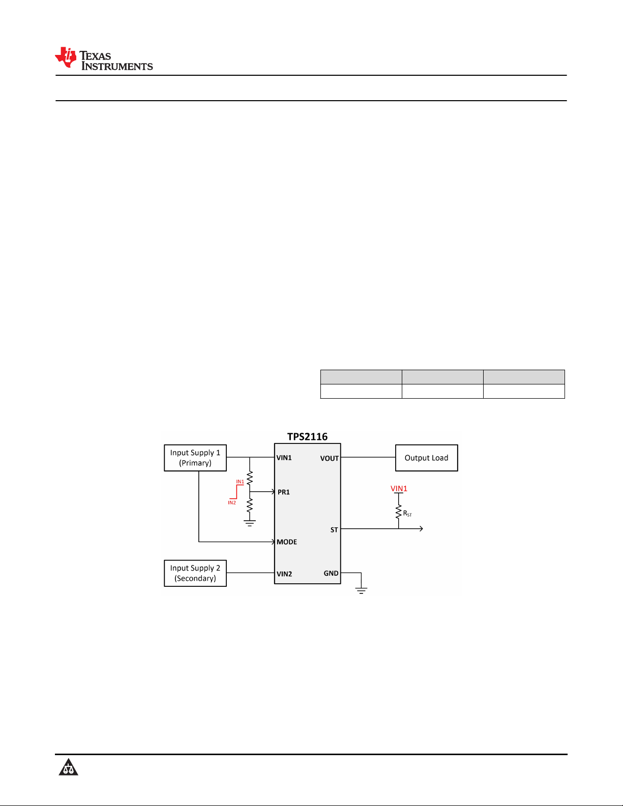
3 Description
The TPS2116 is a power mux device with a voltage
rating of 1.6 V to 5.5 V and a maximum current rating
of 2.5 A. The device uses N-channel MOSFETs to
switch between supplies while providing a controlled
slew rate when voltage is first applied.
Due to its low quiescent of 1.2 uA (typical) and low
standby current of 50 nA (typical), the TPS2116 is
ideal for systems where a battery is connected to one
of the inputs. These low currents extend the life and
operation of the battery when in use.
The TPS2116 can be configured for two different
switchover behaviors depending on the application.
Automatic priority mode prioritizes the supply
connected to VIN1 and switches over to the
secondary supply (VIN2) when VIN1 drops. Manual
mode allows the user to toggle a GPIO or enable
signal to switch between channels.
Device Information
PART NUMBER PACKAGE BODY SIZE (NOM)
TPS2116 SOT (8) 2.1 mm x 1.6 mm
(1) For all available packages, see the orderable addendum at
the end of the data sheet.
(1)
Basic Application
An IMPORTANT NOTICE at the end of this data sheet addresses availability, warranty, changes, use in safety-critical applications,
Copyright © 2021 Texas Instruments Incorporated
intellectual property matters and other important disclaimers. ADVANCE INFORMATION for preproduction products; subject to change
without notice.
Product Folder Links: TPS2116
Submit Document Feedback
1
TPS2116
ADVANCE INFORMATION
SLVSFG1 – JANUARY 2021
www.ti.com
Table of Contents
1 Features............................................................................1
2 Applications..................................................................... 1
3 Description.......................................................................1
4 Revision History.............................................................. 2
5 Pin Configuration and Functions...................................3
6 Specifications.................................................................. 4
6.1 Absolute Maximum Ratings ....................................... 4
6.2 ESD Ratings .............................................................. 4
6.3 Recommended Operating Conditions ........................4
6.4 Thermal Information ...................................................4
6.5 Electrical Characteristics ............................................5
6.6 Switching Characteristics ...........................................6
6.7 Typical Characteristics................................................7
7 Detailed Description........................................................8
7.1 Overview..................................................................... 8
7.2 Functional Block Diagram........................................... 8
7.3 Feature Description.....................................................8
7.4 VINx Collapse Rate.....................................................9
4 Revision History
DATE REVISION NOTES
January 2021 * Initial release.
7.5 Output Voltage Drop................................................... 9
7.6 Device Functional Modes............................................9
8 Application and Implementation.................................. 11
8.1 Application Information..............................................11
8.2 Typical Application.................................................... 11
8.3 Application Limitations.............................................. 12
9 Power Supply Recommendations................................13
10 Layout...........................................................................14
10.1 Layout Guidelines................................................... 14
10.2 Layout Example...................................................... 14
11 Device and Documentation Support..........................15
11.1 Documentation Support.......................................... 15
11.2 Receiving Notification of Documentation Updates..15
11.3 Trademarks............................................................. 15
11.4 Electrostatic Discharge Caution..............................15
11.5 Glossary..................................................................15
12 Mechanical, Packaging, and Orderable
Information.................................................................... 15
2 Submit Document Feedback
Copyright © 2021 Texas Instruments Incorporated
Product Folder Links: TPS2116
www.ti.com
ADVANCE INFORMATION
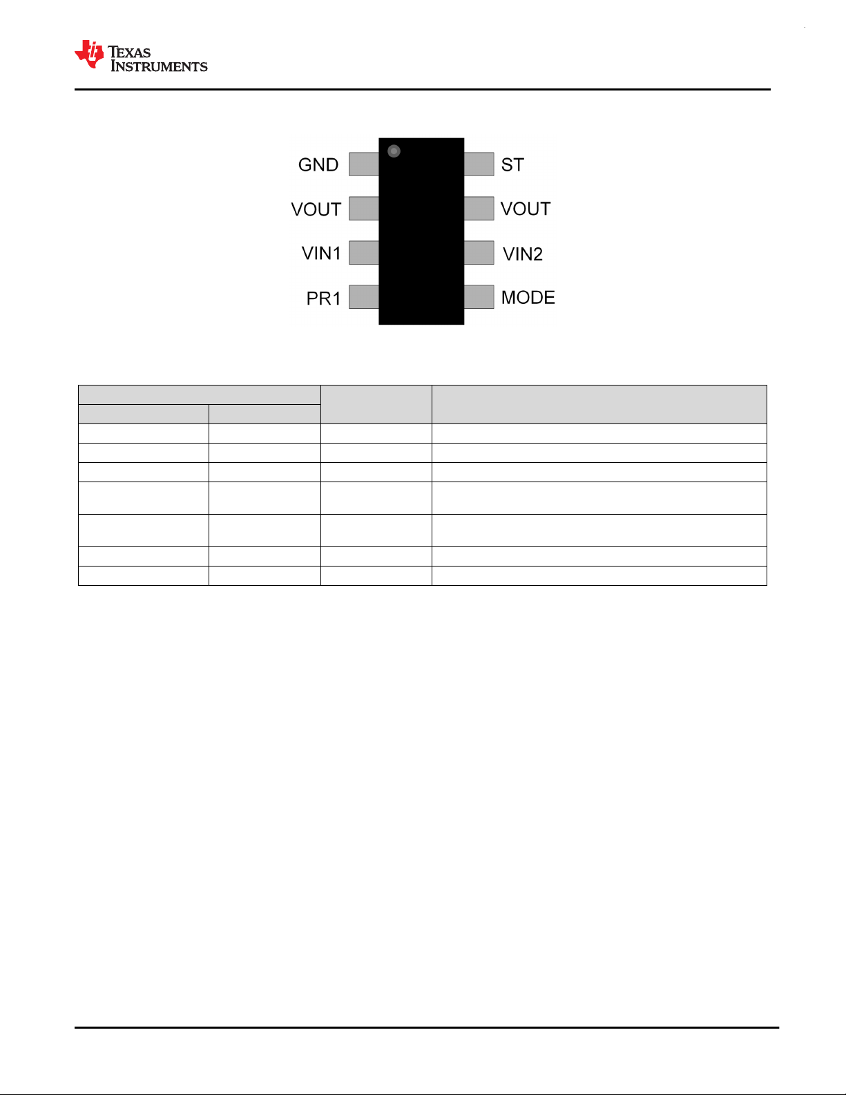
5 Pin Configuration and Functions
Figure 5-1. DRL Package 8-Pin SOT Top View
PIN
NAME NO.
GND 1 - Device ground.
VOUT 2, 7 O Output power.
VIN1 3 I Channel 1 input power.
PR1 4 I
MODE 5 I
VIN2 6 I Channel 2 input power.
ST 8 O Open drain status pin. Pulled low when VIN1 is not being used.
SLVSFG1 – JANUARY 2021
TPS2116
Table 5-1. Pin Functions
I/O DESCRIPTION
Selects between VIN1 and VIN2. When PR1 is high VIN1 is
selected, and when PR1 is low VIN2 is selected.
Device is put into Priority mode when MODE is tied to VIN1 and
manual mode when MODE is pulled up to an external voltage.
Copyright © 2021 Texas Instruments Incorporated
Product Folder Links: TPS2116
Submit Document Feedback
3

ADVANCE INFORMATION
TPS2116
SLVSFG1 – JANUARY 2021
www.ti.com
6 Specifications
6.1 Absolute Maximum Ratings
over operating free-air temperature range (unless otherwise noted)
V
, V
IN1
IN2
V
OUT
VST, V
PR1
V
MODE
I
MAX
I
MAX,PLS
T
J
T
stg
(1) Stresses beyond those listed under Absolute Maximum Rating may cause permanent damage to the device. These are stress ratings
only, which do not imply functional operation of the device at these or any other conditions beyond those indicated under
Recommended Operating Condition. Exposure to absolute-maximum-rated conditions for extended periods may affect device
reliability.
Input Voltage –0.3 6 V
Output Voltage –0.3 6 V
,
Control Pin Voltage –0.3 6 V
Maximum Current 2.5 A
Maximum Pulsed Current
Max duration 1 ms, Duty cycle of 2%
Junction temperature
Storage temperature –65 150 °C
6.2 ESD Ratings
Human body model (HBM), per ANSI/ESDA/
V
(ESD)
Electrostatic discharge
JEDEC JS-001, all pins
Charged device model (CDM), per JEDEC
specification JESD22-C101, all pins
(1)
MIN MAX UNIT
4 A
Internally
Limited
°C
VALUE UNIT
(1)
±2000
V
(2)
±500
(1) JEDEC document JEP155 states that 500-V HBM allows safe manufacturing with a standard ESD control process.
(2) JEDEC document JEP157 states that 250-V CDM allows safe manufacturing with a standard ESD control process.
6.3 Recommended Operating Conditions
over operating free-air temperature range (unless otherwise noted)
MIN NOM MAX UNIT
V
IN1, VIN2
V
OUT
VST,
V
MODE
V
PR1
T
A
Input Voltage 1.6 5.5 V
Output Voltage 0 5.5 V
,
Control Pin Voltage 0 5.5 V
Ambient Temperature –40 105 °C
6.4 Thermal Information
TPS2116
(1)
8-PINS
R
θJA
R
θJC(top)
R
θJB
Ψ
JT
Ψ
JB
THERMAL METRIC
Junction-to-ambient thermal resistance 111.5 °C/W
Junction-to-case (top) thermal resistance 19.4 °C/W
Junction-to-board thermal resistance 35.8 °C/W
Junction-to-top characterization parameter 1.2 °C/W
Junction-to-board characterization parameter 19.1 °C/W
UNITDRL (SOT)
4 Submit Document Feedback
Copyright © 2021 Texas Instruments Incorporated
Product Folder Links: TPS2116
ADVANCE INFORMATION
www.ti.com
SLVSFG1 – JANUARY 2021
6.4 Thermal Information (continued)
TPS2116
TPS2116
THERMAL METRIC
(1)
UNITDRL (SOT)
8-PINS
R
θJC(bot)
Junction-to-case (bottom) thermal resistance N/A °C/W
(1) For more information about traditional and new thermal metrics, see the Semiconductor and IC Package Thermal Metrics application
report.
6.5 Electrical Characteristics
Over operating free-air temperature range and operating voltage range of 1.6V to 5.5V (unless otherwise noted). Typical
specifications are at an input voltage of 3.3V and ambient temperature of 25°C.
PARAMETER TEST CONDITIONS T
Power Consumption
I
STBY,
VIN1
I
STBY,
VIN2
I
Q, VIN1
I
Q, VIN2
I
PR1
I
MODE
I
ST
VIN1 Standby Current
VIN2 Standby Current
VIN1 Quiescent Current
VIN2 Quiescent Current
PR1 pin leakage –40°C to 105°C 0.03 uA
MODE pin leakage –40°C to 105°C 0.03 uA
ST pin leakage –40°C to 105°C 0.03 uA
Performance
VIN2 powers VOUT
VIN1 > VIN2 + 0.1 V
VIN2 powers VOUT
VIN1 + 0.1 V < VIN2
VIN1 powers VOUT
VIN2 > VIN1 + 0.1 V
VIN1 powers VOUT
VIN2 + 0.1 V < VIN1
VIN1 powers VOUT
VIN1 > VIN2 + 0.1 V
VIN1 powers VOUT
VIN1 + 0.1 V < VIN2
VIN2 powers VOUT
VIN2 > VIN1 + 0.1 V
VIN2 powers VOUT
VIN2 + 0.1 V < VIN1
A
25°C 1.2 uA
–40°C to 85°C 1.9 uA
–40°C to 105°C 2 uA
25°C 0.2 uA
–40°C to 85°C 0.31 uA
–40°C to 105°C 0.32 uA
25°C 1.2 uA
–40°C to 85°C 2 uA
–40°C to 105°C 2.1 uA
25°C 0.05 uA
–40°C to 85°C 0.07 uA
–40°C to 105°C 0.09 uA
25°C 1.25 uA
–40°C to 85°C 3.6 uA
–40°C to 105°C 4.4 uA
25°C 0.3 uA
–40°C to 85°C 0.51 uA
–40°C to 105°C 0.55 uA
25°C 1.3 uA
–40°C to 85°C 3.7 uA
–40°C to 105°C 4.5 uA
25°C 0.15 uA
–40°C to 85°C 0.27 uA
–40°C to 105°C 0.29 uA
MIN TYP MAX UNIT
Copyright © 2021 Texas Instruments Incorporated
Product Folder Links: TPS2116
Submit Document Feedback
5
ADVANCE INFORMATION
TPS2116
SLVSFG1 – JANUARY 2021
www.ti.com
6.5 Electrical Characteristics (continued)
Over operating free-air temperature range and operating voltage range of 1.6V to 5.5V (unless otherwise noted). Typical
specifications are at an input voltage of 3.3V and ambient temperature of 25°C.
PARAMETER TEST CONDITIONS T
A
25°C 37 46 mΩ
VINx = 5 V
I
= 200 mA
OUT
–40°C to 85°C 55 mΩ
–40°C to 105°C 60 mΩ
25°C 40 48 mΩ
VINx = 3.3 V
I
= 200mA
OUT
R
ON
On-Resistance
VINx = 1.8 V
I
= 200 mA
OUT
–40°C to 85°C 55 mΩ
–40°C to 105°C 59 mΩ
25°C 41 51 mΩ
–40°C to 85°C 61 mΩ
–40°C to 105°C 66 mΩ
25°C 42 52 mΩ
V
OL,ST
t
ST
V
REF
V
IH,
MODE
V
IL,
MODE
VINx = 1.6 V
I
= 200 mA
OUT
Status pin V
OL
IST = 1 mA –40°C to 105°C 0.1 V
Status pin response time RST = 10 kΩ –40°C to 105°C 5 us
PR1 reference voltage –40°C to 105°C 0.92 1 1.08 V
MODE logic high threshold –40°C to 105°C 1 5.5 V
MODE logic low threshold –40°C to 105°C 0 0.35 V
–40°C to 85°C 68 mΩ
–40°C to 105°C 74 mΩ
Protection
t
RCB
V
V
I
RCB
Reverse current blocking response
time
Reverse current blocking rising
RCB,R
threshold (V
Reverse current blocking falling
RCB,F
threshold (V
OUT
OUT
- VIN)
- VIN)
Reverse current blocking activation
current
VOUT > Selected VIN + 1 V –40°C to 105°C 2 us
–40°C to 105°C 42 70 mV
1.6 V ≤ VINx ≤ 5.5 V –40°C to 105°C 17 40 mV
1.6 V ≤ VINx ≤ 5.5 V –40°C to 105°C 1.4 4 A
TSD Thermal shutdown - 170 °C
TSD
Thermal shutdown hysteresis - 20 °C
HYS
MIN TYP MAX UNIT
6.6 Switching Characteristics
Typical switching characteristics are defined at an ambient temperature of 25°C
PARAMETER TEST CONDITIONS MIN TYP MAX UNIT
Switchover
t
SW
t
SW
t
SW
t
D
t
D
t
D
t
SS
t
SS
t
SS
6 Submit Document Feedback
Switchover time, VINx = 5V RL = 10 Ω, CL = 10 uF 8 us
Switchover time, VINx = 3.3V RL = 10 Ω, CL = 10 uF 6.2 us
Switchover time, VINx = 1.8V RL = 10 Ω, CL = 10 uF 17.7 us
Delay time, VINx = 5V RL = 100 Ω, CL = 10 uF 1 ms
Delay time, VINx = 3.3V RL = 100 Ω, CL = 10 uF 1.2 ms
Delay time, VINx = 1.8V RL = 100 Ω, CL = 10 uF 1.4 ms
Soft-start time, VINx = 5V RL = 100 Ω, CL = 10 uF 1.7 ms
Soft-start time, VINx = 3.3V RL = 100 Ω, CL = 10 uF 1.3 ms
Soft-start time, VINx = 1.8V RL = 100 Ω, CL = 10 uF 0.9 ms
Product Folder Links: TPS2116
Copyright © 2021 Texas Instruments Incorporated
www.ti.com
ADVANCE INFORMATION
6.7 Typical Characteristics
SLVSFG1 – JANUARY 2021
TPS2116
Figure 6-1. Priority Mode Switchover Behavior
Copyright © 2021 Texas Instruments Incorporated
Product Folder Links: TPS2116
Submit Document Feedback
7

TPS2116
ADVANCE INFORMATION
SLVSFG1 – JANUARY 2021
www.ti.com
7 Detailed Description
7.1 Overview
The TPS2116 is a power mux device with a voltage rating of 1.6 V to 5.5 V and a maximum current rating of 2.5
A. The device uses N-channel MOSFETs to switch between supplies while providing a controlled slew rate when
voltage is first applied.
The TPS2116 can be configured for two different switchover behaviors depending on the application. Automatic
priority mode prioritizes the supply connected to VIN1 and switches over to the secondary supply (VIN2) when
VIN1 drops. Manual mode allows the user to toggle a GPIO or enable signal to switch between channels.
Due to its low quiescent of 1.2 uA (typical) and standby current of 50 nA (typical), the TPS2116 is ideal for
systems where a battery is connected to one of the inputs. These low currents extend the life and operation of
the battery when in use.
7.2 Functional Block Diagram
7.3 Feature Description
The below sections detail the features of the TPS2116.
7.3.1 Truth Table
The below table shows the expected behavior of the TPS2116.
MODE
VIN1 (Priority)
External Bias
(Manual)
VIN1 VIN2 PR1 ST VOUT
High X
Low ≥ 1.6 V Low VIN2
≥ 1.6 V X High High VIN1
X ≥ 1.6 V Low Low VIN2
VIN1 through resistor
High VIN1
divider
X = don't care
7.3.2 Soft Start
When an input voltage is applied to the TPS2116 and the output voltage is lower than 1 V, the output will be
brought up with soft start to minimize the inrush current due to output capacitance. However, when the device
switches from one power supply to another (switchover) and VOUT > 1 V, soft start is not used to minimize the
8 Submit Document Feedback
Product Folder Links: TPS2116
Copyright © 2021 Texas Instruments Incorporated

www.ti.com
ADVANCE INFORMATION
SLVSFG1 – JANUARY 2021
TPS2116
output voltage drop. For linear soft start behavior, it is recommended to have an output capacitance of at least
0.1 uF.
7.3.3 Status Indication
The ST pin is an open drain output that should be pulled up to an external voltage for proper operation. When
the TPS2116 is powering the output using VIN1, the ST pin will be pulled high by the external voltage source.
When the TPS2116 is powering the output using VIN2, the ST pin will be pulled low. During thermal shutdown,
the ST pin will be pulled low regardless of the channel being used.
7.4 VINx Collapse Rate
The TPS2116 uses the highest voltage supply to power the device. When one supply drops below the other, the
device changes the supply used to power the device. If the supply powering the device drops at a rate faster
than 1 V/10 μs, the other supply must be at 2.5 V or higher to prevent the device from resetting. If the other
supply is lower than 2.5 V, then the device may not be able to switch to the supply quickly enough, and the
device will reset and turn on with soft start timing if VOUT < 1 V.
7.5 Output Voltage Drop
The output voltage drop is based on the load capacitance and load resistance. The stronger the resistive load,
the faster the output will discharge during switchover. The higher the capacitance on the output, the less the
voltage will drop during switchover.
7.6 Device Functional Modes
The below sections detail the two different configuraiton options for the device.
7.6.1 Priority/Manual Mode
When MODE is tied high, PR1 determines the channel selected. To configure VIN1 as the priority supply,
connect MODE to VIN1 and set the proper threshold through a resistor divider from VIN1 to PR1. To configure
manual selection, pull up MODE to an external supply and follow the truth table. When PR1 is pulled above
V
, the voltage on VIN1 is used to power the output, and when it is pulled below V
REF
, VIN2 is used to power
REF
the output. The expected behavior for the device is shown in the waveform below.
Copyright © 2021 Texas Instruments Incorporated
Product Folder Links: TPS2116
Submit Document Feedback
9

TPS2116
ADVANCE INFORMATION
SLVSFG1 – JANUARY 2021
www.ti.com
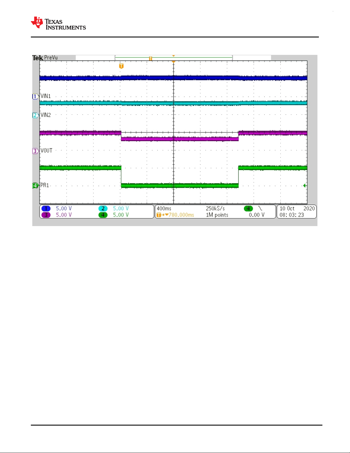
Figure 7-1. Priority/Manual Mode Switching
When PR1 is toggled, the device implements a break-before-make switchover which shuts off both channels
before turning on the new channel to power the output. This means that for time tSW, the output is unpowered
and will dip depending on the load current and output capacitance. If the output voltage is greater than the input
supply being switched to, then the device will not turn on the new channel until the output has discharged down
to VIN + V
to prevent reverse current flow.
RCB
7.6.1.1 Manual Switching
For applications where a GPIO pin is used to select which input passes to the output, the GPIO pin can be
directly connected to the PR1 pin. When the GPIO is pulled high, VIN1 is used, and when the GPIO pin is pulled
low, VIN2 is used.
7.6.1.2 Priority Switching
In the case where VIN1 takes priority over VIN2, a resistor divider can be used to set the switchover voltage
threshold. When VIN1 is first applied, PR1 is brought high and VOUT is powered by that input. As VIN1 begins
to drop, the voltage on PR1 is lowered until it crosses the V
threshold. At this point, the device switches over
REF
to VIN2.
10 Submit Document Feedback
Copyright © 2021 Texas Instruments Incorporated
Product Folder Links: TPS2116

www.ti.com
ADVANCE INFORMATION
SLVSFG1 – JANUARY 2021
TPS2116
8 Application and Implementation
Note
Information in the following applications sections is not part of the TI component specification, and TI
does not warrant its accuracy or completeness. TI’s customers are responsible for determining
suitability of components for their purposes, as well as validating and testing their design
implementation to confirm system functionality.
8.1 Application Information
This section highlights some of the design considerations when implementing this device in various applications.
8.2 Typical Application
This typical application demonstrates how the TPS2116 device can be used to control inrush current for high
output capacitances.
Figure 8-1. TPS2116 Typical Application Diagram
8.2.1 Design Requirements
For this example, the values below are used as the design parameters.
Table 8-1. Design Parameters
PARAMETER VALUE
VIN1 Input Voltage 5 V
Mode Priority
Output Capacitance 100 µF
Maximum Inrush Current 500 mA
8.2.2 Detailed Design Procedure
To determine how much inrush current is caused by the output capacitor, use the equation below.
Copyright © 2021 Texas Instruments Incorporated
Product Folder Links: TPS2116
Submit Document Feedback
11

TPS2116
ADVANCE INFORMATION
SLVSFG1 – JANUARY 2021
I
= C
INRUSH
OUT
× V
OUT
/ t
SS
www.ti.com
(1)
where
• I
• C
= amount of inrush current caused by C
INRUSH
= capacitance on VOUT
OUT
OUT
• tSS = output voltage soft start time
• V
= final value of the output voltage
OUT
With a final output voltage of 5 V, the expected rise time is 1.7 ms. Using the inrush current equation, the inrush
current caused by a 100-µF capacitance would be 294 mA, well below the 500-mA target.
8.2.3 Application Curves
The below oscilloscope capture shows 5 V being applied to VIN1. The output comes up with slew rate control
and limits the inrush current to below 500 mA.
Figure 8-2. TPS2116 Inrush Current Control
8.3 Application Limitations
With current preliminary silicon, the TPS2116 may have an increased slew rate (and therefore increased inrush
current) when only one supply is used to power the device. The device behaves normally when the power supply
is first connected, but when the supply is removed and replaced too quickly the output may rise up faster than
datasheet specifications. If the time between power cycles is less than approximately 5 seconds, the output slew
rate may be faster than expected, resulting in higher inrush current. The time needed between power cycles to
avoid a faster slew rate increases with colder temperatures. This will be revised in the final silicon to provide
slew rate control when fast power cycling occurs. The Application Limitation section will be removed once final
silicon has been released.
12 Submit Document Feedback
Copyright © 2021 Texas Instruments Incorporated
Product Folder Links: TPS2116

www.ti.com
ADVANCE INFORMATION
SLVSFG1 – JANUARY 2021
TPS2116
9 Power Supply Recommendations
The device is designed to operate with a VIN range of 1.6 V to 5.5 V. The VIN power supplies must be well
regulated and placed as close to the device terminals as possible. The power supplies must be able to withstand
all transient load current steps. In most situations, using an input capacitance (CIN) of 1 μF is sufficient to prevent
the supply voltage from dipping when the switch is turned on. In cases where the power supply is slow to
respond to a large transient current or large load current step, additional bulk capacitance may be required on
the input.
Copyright © 2021 Texas Instruments Incorporated
Product Folder Links: TPS2116
Submit Document Feedback
13

TPS2116
ADVANCE INFORMATION
SLVSFG1 – JANUARY 2021
www.ti.com
10 Layout
10.1 Layout Guidelines
For best performance, all traces must be as short as possible. To be most effective, the input and output
capacitors must be placed close to the device to minimize the effects that parasitic trace inductances may have
on normal operation. Using wide traces for VIN1, VIN2, VOUT, and GND helps minimize the parasitic electrical
effects.
10.2 Layout Example
14 Submit Document Feedback
Figure 10-1. TPS2116 Layout Example
Copyright © 2021 Texas Instruments Incorporated
Product Folder Links: TPS2116

www.ti.com
ADVANCE INFORMATION
SLVSFG1 – JANUARY 2021
TPS2116
11 Device and Documentation Support
11.1 Documentation Support
11.1.1 Related Documentation
For related documentation see the following:
• Basics of Power MUX
• 11 Ways to Protect Your Power Path
11.2 Receiving Notification of Documentation Updates
To receive notification of documentation updates, navigate to the device product folder on ti.com. Click on
Subscribe to updates to register and receive a weekly digest of any product information that has changed. For
change details, review the revision history included in any revised document.
11.3 Trademarks
All trademarks are the property of their respective owners.
11.4 Electrostatic Discharge Caution
This integrated circuit can be damaged by ESD. Texas Instruments recommends that all integrated circuits be handled
with appropriate precautions. Failure to observe proper handling and installation procedures can cause damage.
ESD damage can range from subtle performance degradation to complete device failure. Precision integrated circuits may
be more susceptible to damage because very small parametric changes could cause the device not to meet its published
specifications.
11.5 Glossary
TI Glossary This glossary lists and explains terms, acronyms, and definitions.
12 Mechanical, Packaging, and Orderable Information
The following pages include mechanical, packaging, and orderable information. This information is the most
current data available for the designated devices. This data is subject to change without notice and revision of
this document. For browser-based versions of this data sheet, refer to the left-hand navigation.
Copyright © 2021 Texas Instruments Incorporated
Product Folder Links: TPS2116
Submit Document Feedback
15

PACKAGE OPTION ADDENDUM
www.ti.com
PACKAGING INFORMATION
Orderable Device Status
PTPS2116DRLR ACTIVE SOT-5X3 DRL 8 4000 Non-RoHS &
TPS2116DRLR PREVIEW SOT-5X3 DRL 8 4000 Non-RoHS &
(1)
The marketing status values are defined as follows:
ACTIVE: Product device recommended for new designs.
LIFEBUY: TI has announced that the device will be discontinued, and a lifetime-buy period is in effect.
NRND: Not recommended for new designs. Device is in production to support existing customers, but TI does not recommend using this part in a new design.
PREVIEW: Device has been announced but is not in production. Samples may or may not be available.
OBSOLETE: TI has discontinued the production of the device.
Package Type Package
(1)
Drawing
Pins Package
Qty
Eco Plan
(2)
Non-Green
Non-Green
Lead finish/
Ball material
(6)
Call TI Call TI -40 to 125
Call TI Call TI -40 to 125
MSL Peak Temp
(3)
Op Temp (°C) Device Marking
(4/5)
(2)
RoHS: TI defines "RoHS" to mean semiconductor products that are compliant with the current EU RoHS requirements for all 10 RoHS substances, including the requirement that RoHS substance
do not exceed 0.1% by weight in homogeneous materials. Where designed to be soldered at high temperatures, "RoHS" products are suitable for use in specified lead-free processes. TI may
reference these types of products as "Pb-Free".
RoHS Exempt: TI defines "RoHS Exempt" to mean products that contain lead but are compliant with EU RoHS pursuant to a specific EU RoHS exemption.
Green: TI defines "Green" to mean the content of Chlorine (Cl) and Bromine (Br) based flame retardants meet JS709B low halogen requirements of <=1000ppm threshold. Antimony trioxide based
flame retardants must also meet the <=1000ppm threshold requirement.
(3)
MSL, Peak Temp. - The Moisture Sensitivity Level rating according to the JEDEC industry standard classifications, and peak solder temperature.
(4)
There may be additional marking, which relates to the logo, the lot trace code information, or the environmental category on the device.
(5)
Multiple Device Markings will be inside parentheses. Only one Device Marking contained in parentheses and separated by a "~" will appear on a device. If a line is indented then it is a continuation
of the previous line and the two combined represent the entire Device Marking for that device.
(6)
Lead finish/Ball material - Orderable Devices may have multiple material finish options. Finish options are separated by a vertical ruled line. Lead finish/Ball material values may wrap to two
lines if the finish value exceeds the maximum column width.
Important Information and Disclaimer:The information provided on this page represents TI's knowledge and belief as of the date that it is provided. TI bases its knowledge and belief on information
provided by third parties, and makes no representation or warranty as to the accuracy of such information. Efforts are underway to better integrate information from third parties. TI has taken and
continues to take reasonable steps to provide representative and accurate information but may not have conducted destructive testing or chemical analysis on incoming materials and chemicals.
TI and TI suppliers consider certain information to be proprietary, and thus CAS numbers and other limited information may not be available for release.
In no event shall TI's liability arising out of such information exceed the total purchase price of the TI part(s) at issue in this document sold by TI to Customer on an annual basis.
9-Mar-2021
Samples
Addendum-Page 1

PACKAGE OPTION ADDENDUM
www.ti.com
9-Mar-2021
Addendum-Page 2

PACKAGE OUTLINE
ID AREA
6X 0.5
2X 1.5
0.27
8X
0.17
0.1 C A B
0.05
PIN 1
SCALE 8.000
B
1
4
1.3
1.1
1.7
1.5
A
8
2.2
2.0
NOTE 3
5
SOT-5X3 - 0.6 mm max heightDRL0008A
PLASTIC SMALL OUTLINE
0.05
0.00
0.6 MAX
0.18
0.08
8X
0.4
SYMM
0.2
SYMM
C
SEATING PLANE
0.05 C
4224486/B 03/2021
NOTES:
1. All linear dimensions are in millimeters. Any dimensions in parenthesis are for reference only. Dimensioning and tolerancing
per ASME Y14.5M.
2. This drawing is subject to change without notice.
3. This dimension does not include mold flash, protrusions, or gate burrs. Mold flash, interlead flash, protrusions, or gate burrs shall not
exceed 0.15 mm per side.
4. Reference JEDEC registration TO-236, except minimum foot length.
www.ti.com

8X (0.67)
EXAMPLE BOARD LAYOUT
SOT-5X3 - 0.6 mm max heightDRL0008A
PLASTIC SMALL OUTLINE
SYMM
0.05 MAX
AROUND
8X (0.3)
6X (0.5)
(R0.05) TYP
1
4
(1.48)
8
SYMM
5
LAND PATTERN EXAMPLE
EXPOSED METAL SHOWN
SCALE:30X
0.05 MIN
AROUND
EXPOSED
METAL
SOLDER MASK
OPENING
METAL
NON SOLDER MASK
DEFINED
(PREFERRED)
EXPOSED
METAL
METAL UNDER
SOLDER MASK
SOLDER MASK
DEFINED
SOLDERMASK DETAILS
NOTES: (continued)
5. Publication IPC-7351 may have alternate designs.
6. Solder mask tolerances between and around signal pads can vary based on board fabrication site.
SOLDER MASK
OPENING
4224486/B 03/2021
www.ti.com

EXAMPLE STENCIL DESIGN
SOT-5X3 - 0.6 mm max heightDRL0008A
PLASTIC SMALL OUTLINE
8X (0.3)
6X (0.5)
(R0.05) TYP
1
4
8X (0.67)
SYMM
(1.48)
SOLDER PASTE EXAMPLE
BASED ON 0.1 mm THICK STENCIL
SCALE:30X
8
SYMM
5
4224486/B 03/2021
NOTES: (continued)
7. Laser cutting apertures with trapezoidal walls and rounded corners may offer better paste release. IPC-7525 may have alternate
design recommendations.
8. Board assembly site may have different recommendations for stencil design.
www.ti.com

IMPORTANT NOTICE AND DISCLAIMER
TI PROVIDES TECHNICAL AND RELIABILITY DATA (INCLUDING DATASHEETS), DESIGN RESOURCES (INCLUDING REFERENCE
DESIGNS), APPLICATION OR OTHER DESIGN ADVICE, WEB TOOLS, SAFETY INFORMATION, AND OTHER RESOURCES “AS IS”
AND WITH ALL FAULTS, AND DISCLAIMS ALL WARRANTIES, EXPRESS AND IMPLIED, INCLUDING WITHOUT LIMITATION ANY
IMPLIED WARRANTIES OF MERCHANTABILITY, FITNESS FOR A PARTICULAR PURPOSE OR NON-INFRINGEMENT OF THIRD
PARTY INTELLECTUAL PROPERTY RIGHTS.
These resources are intended for skilled developers designing with TI products. You are solely responsible for (1) selecting the appropriate
TI products for your application, (2) designing, validating and testing your application, and (3) ensuring your application meets applicable
standards, and any other safety, security, or other requirements. These resources are subject to change without notice. TI grants you
permission to use these resources only for development of an application that uses the TI products described in the resource. Other
reproduction and display of these resources is prohibited. No license is granted to any other TI intellectual property right or to any third party
intellectual property right. TI disclaims responsibility for, and you will fully indemnify TI and its representatives against, any claims, damages,
costs, losses, and liabilities arising out of your use of these resources.
TI’s products are provided subject to TI’s Terms of Sale (https:www.ti.com/legal/termsofsale.html) or other applicable terms available either
on ti.com or provided in conjunction with such TI products. TI’s provision of these resources does not expand or otherwise alter TI’s
applicable warranties or warranty disclaimers for TI products.IMPORTANT NOTICE
Mailing Address: Texas Instruments, Post Office Box 655303, Dallas, Texas 75265
Copyright © 2021, Texas Instruments Incorporated
 Loading...