

Page 1
TPS2074, TPS2075
TAUSB HUB POWER CONTROLLERS
Four-port with internal LDO controller
32
40°C to 85°C
Four-port without internal LDO controller
24
FOUR-PORT USB HUB POWER CONTROLLERS
SLVS288A – SEPTEMBER 2000 – REVISED FEBRUAR Y 2001
D
Complete USB Hub Power Solution
D
Meets USB Specifications 1.1 and 2.0
D
Independent Thermal and Short-Circuit
Protection
D
3.3-V Regulator for USB Hub Controller
D
Overcurrent Logic Outputs
D
4.5-V to 5.5-V Operating Range
D
CMOS- and TTL-Compatible Enable Inputs
D
185 µA Bus-Power Supply Current
D
Available in 24-Pin SSOP Package
D
–40°C to 85°C Ambient Temperature Range
description
The TPS2074 and TPS2075 provide a complete
USB hub power solution by incorporating three
major functions: current-limited power switches
for four ports, a 3.3-V 100-mA regulator, and a
DP0 line control to signal attach/detach of the hub.
These devices are designed to meet bus-powered and self-powered hub requirements. These
PG_DLY
AGND
3.3V_OUT
BPMODE
DP0_RST
DGND
NC – No internal connection
†
Pin 9 is active low (BPMODE
and active high (BPMODE) for TPS2075.
simplified hybrid-hub diagram
Power
Supply
DB PACKAGE
EN1
PG
SP
SP
NC
†
EN2
SP
devices are also designed for hybrid hub
implementations and allow for automatic switching from self-powered mode to bus-powered
mode if loss of self-power is experienced. This
feature can be disabled by applying a logic high to
the BP_DIS input
Each port has a current-limited 100-mΩ Nchannel MOSFET high-side power switch for
500 mA self-powered operation. Each port also
has a current-limited 500-mΩ N-channel MOS-
FET high-side power switch for 100-mA buspowered operation. All the N-channel MOSFETs
Upstream
Port
D+
D–
5 V
GND
1.5
kΩ
DP0_RST
BP
3.3 V_OUT BPMODE
VCCEN OC
DP0
DM0
are designed without parasitic diodes, preventing
current backflow into the inputs.
‡
For applications where a 5-V regulator is needed,
See Figure 33 for complete implementation.
use the TPS2070 or TPS2071 device.
SELECTION GUIDE
PACKAGED DEVICES
PIN COUNT BPMODE HTSSOP (DAP) SSOP (DB)
p
–
p
†
The DB package is available taped and reeled. Add an R suffix to the device type (e.g., TPS2074DBR).
Active low TPS2070DAP —
Active high TPS2071DAP —
Active low — TPS2074DB
Active high — TPS2075DB
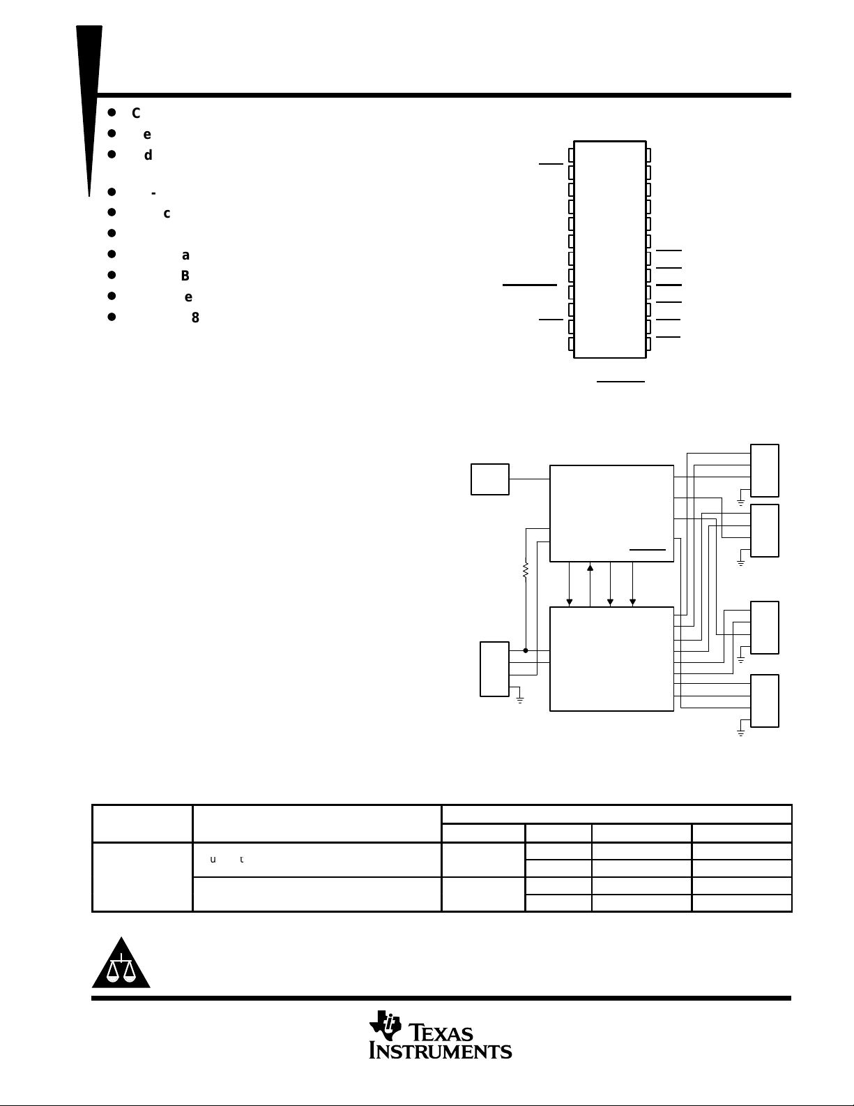
(TOP VIEW)
1
2
3
4
5
6
7
8
9
10
11
12
TPS2074
Hub
Controller
BP_DIS
24
BP
23
OUT1
22
OUT2
21
OUT3
20
OUT4
19
OC4
18
OC3
17
OC2
16
OC1
15
EN4
14
EN3
13
) for TPS2074
OUT1
OUT2
OUT3
OUT4
DP1
DM1
DP2
DM2
DP3
DM3
DP4
DM4
‡
D+
D–
5 V
GND
D+
D–
5 V
GND
Downstream
Ports
D+
D–
5 V
GND
D+
D–
5 V
GND
†
Please be aware that an important notice concerning availability, standard warranty, and use in critical applications of
Texas Instruments semiconductor products and disclaimers thereto appears at the end of this data sheet.
PRODUCTION DATA information is current as of publication date.
Products conform to specifications per the terms of Texas Instruments
standard warranty. Production processing does not necessarily include
testing of all parameters.
POST OFFICE BOX 655303 • DALLAS, TEXAS 75265
Copyright 2001, Texas Instruments Incorporated
1
Page 2
TPS2074, TPS2075
FOUR-PORT USB HUB POWER CONTROLLERS
SLVS288A – SEPTEMBER 2000 – REVISED FEBRUARY 2001
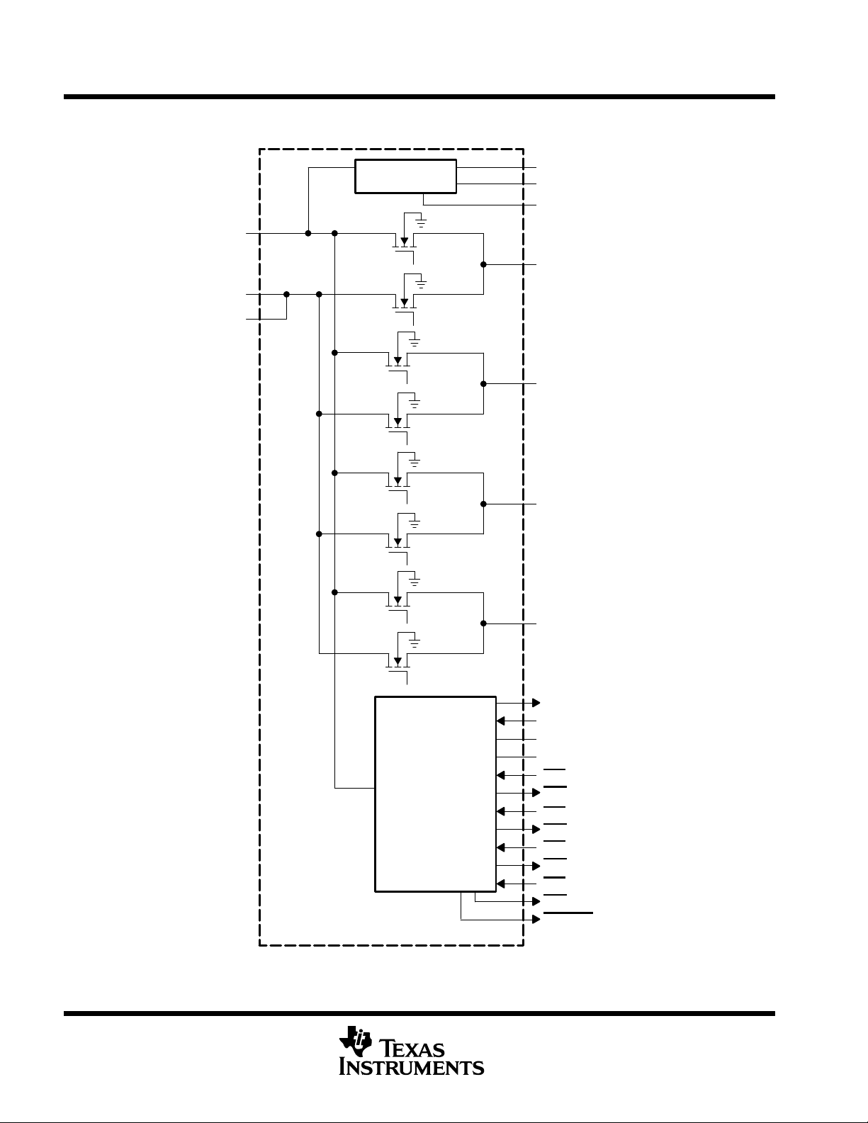
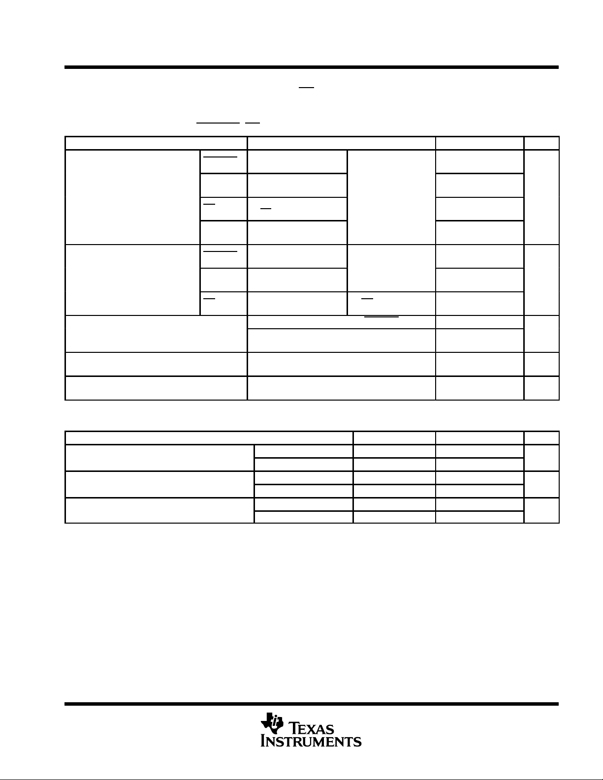
functional block diagram
BP
SP
SP
3.3 V/100 mA LDO
S1
S2
S3
S4
S5
S6
3.3 V_OUT
PG
PG_DLY
OUT1
OUT2
OUT3
S7
S8
Control
Logic
OUT4
DPO_RST
BP_DIS
AGND
DGND
EN1
OC1
EN2
OC2
EN3
OC3
EN4
OC4
BPMODE (TPS2074)
BPMODE (TPS2075)
2
POST OFFICE BOX 655303 • DALLAS, TEXAS 75265
Page 3
TPS2074, TPS2075
I/O
DESCRIPTION
FOUR-PORT USB HUB POWER CONTROLLERS
SLVS288A – SEPTEMBER 2000 – REVISED FEBRUARY 2001
Terminal Functions
TERMINAL
NAME NO.
PG_DLY
EN1 2 I Active-low enable for OUT1
AGND 3 Analog ground
PG 4 O Logic output, power good
SP 5 I Self-power voltage input, connects to local power supply
SP 6 I Self-power voltage input, connects to local power supply
NC 7 No internal connection
3.3V_OUT 8 O 3.3-V internal voltage regulator output
BPMODE
DP0_RST 10 O Connects to DP signal from upstream hub/host through an external 1.5-kΩ resistor
EN2 11 I Active-low enable for OUT2
DGND 12 Digital ground
EN3 13 I Active-low enable for OUT3
EN4 14 I Active-low enable for OUT4
OC1 15 O Logic output, overcurrent response for OUT1
OC2 16 O Logic output, overcurrent response for OUT2
OC3 17 O Logic output, overcurrent response for OUT3
OC4 18 O Logic output, overcurrent response for OUT4
OUT4 19 O Power switch output for downstream ports
OUT3 20 O Power switch output for downstream ports
OUT2 21 O Power switch output for downstream ports
OUT1 22 O Power switch output for downstream ports
BP 23 I Bus power voltage input, connect to V
BP_DIS 24 I Active-high logic input, disables autoswitch to bus power when self power is disconnected. Connect to BP or GND
†
‡
†
1 Adjusts the PG time delay with a capacitor to ground. Adjust the pulse width to fit the application.
‡
9 O A logic signal that indicates if the outputs source from the bus-powered supply, BPMODE (TPS2074) or BPMODE
Use the following formula to calculate the capacitance needed;
C = (desired pulse width × 3 × 10⁻⁶ / 1.22
Pin 9 is active low for TPS2074 and active high for TPS2075.
(TPS2075), can be used to signal the hub controller.
BUS
POST OFFICE BOX 655303 • DALLAS, TEXAS 75265
3
Page 4

TPS2074, TPS2075
FOUR-PORT USB HUB POWER CONTROLLERS
SLVS288A – SEPTEMBER 2000 – REVISED FEBRUARY 2001
detailed description
BP
The bus-powered supply input (BP) serves as the source for the internal 3.3-V LDO and for all logic functions
in the device. In bus-powered mode, BP also serves as the source for all the outputs (OUTx). If BP is below the
undervoltage threshold, all power switches will turn off and the LDO will be disabled. BP must be connected to
a voltage source in order for the device to operate.
SP
The self-powered supply input (SP) serves as the source for all the outputs (OUTx) in self-powered mode. The
enable logic for the SP switches requires that BP be connected to a voltage source.
OUT1, OUT2, OUT2, OUT4
OUTx are the outputs of the integrated power switches.
3.3V_OUT
The internal 3.3-V LDO output can be used to supply up to 100 mA current to low-power functions, such as hub
controllers.
DP0_RST
DP0_RST functions as a hub reset when a 1.5-kΩ resistor is connected between DP0_RST and the upstream
DP0 data line in a hub system. To provide a clean attach signal on DP0 data line, the DP0_RST output goes
low momentarily (because of the upstream pulldown resistor) to discharge any parasitic charge on the cable,
then goes to 3-state and finally outputs a high signal. The low and Hi-Z pulse widths are adjustable using a
capacitor between PG_DL Y and ground, and are approximately 50% of the power-good time delay. Detachment
is signaled by a Hi-Z on DP0_RST. Both DP0_RST and PG will transition high at the same time.
Power Good (PG)
The power good (PG) function serves as a reset for a USB hub controller. PG is asserted low when the output
voltage on the internal voltage regulator is below a fixed threshold. A time delay to ensure a stable output voltage
before PG goes high is adjustable using a small-value ceramic capacitor from PG_DLY to ground.
PG_DLY
PG_DL Y connects to an external capacitor to adjust the time delay for PG and DP0_RST . For USB applications,
a 0.1 µF capacitor is recommended, however, reference the USB hub controller data sheet to determine the
needed pulse width criteria.
BP_DIS
BP_DIS is used to enable or disable the autoswitching function between bus-powered mode and self-powered
mode. When BP_DIS is connected low and the voltage on SP is greater than the undervoltage-lockout (UVLO)
threshold, the device will switch to self-powered operation automatically; if the SP voltage falls lower than the
UVLO threshold, the device will switch to bus-powered operation. When BP_DIS is connected high, the
autoswitching function is disabled and the device will not autoswitch to bus-powered operation if the SP voltage
is below the UVLO threshold.
BPMODE
4
or BPMODE
BPMODE
mode. The logic state is set according to the voltages on BP, SP, and BP_DIS. For the TPS2074, BPMODE
outputs a low signal to indicate bus-powered mode or a high signal to indicate self-powered mode. For the
TPS2075, BPMODE outputs a high signal to indicate bus-powered mode or a low signal to indicate self-powered
mode. This output can be used to inform a USB hub controller to configure for bus-powered mode or
self-powered mode.
(TPS2074) or BPMODE (TPS2075) is an output that signals when the device is in bus-powered
POST OFFICE BOX 655303 • DALLAS, TEXAS 75265
Page 5
TPS2074, TPS2075
Input voltage
V
O
FOUR-PORT USB HUB POWER CONTROLLERS
SLVS288A – SEPTEMBER 2000 – REVISED FEBRUARY 2001
detailed description (continued)
OC1, OC2, OC3, OC4
OCx is an output signal that is asserted (active low) when an overcurrent or overtemperature condition is
encountered for the corresponding channel. OCx
condition is removed.
, EN2, EN3, EN4,
EN1
will remain asserted until the overcurrent or overtemperature
The active-low logic input ENx
enables or disables the power switches in the device. The enable input is
compatible with both TTL and CMOS logic levels. The switches will not turn on until 3.3V_OUT is above the PG
threshold.
absolute maximum ratings over operating free-air temperature range (unless otherwise noted)
Input voltage range: V
Output voltage range: V
, V
I(BP)
O(OUTx)
V
O(3.3V_OUT)
V
O(DP0_RST)
Continuous output current: I
Maximum output current: I
Continuous total power dissipation See Dissipation Rating Table. . . . . . . . . . . . . . . . . . . . . . . . . . . . . . . . . . . . . .
Operating virtual junction temperature range, T
Storage temperature range, T
Lead temperature soldering 1,6 mm (1/16 inch) from case for 10 seconds 260°C. . . . . . . . . . . . . . . . . . . . . . .
†
Stresses beyond those listed under “absolute maximum ratings” may cause permanent damage to the device. These are stress ratings only, and
functional operation of the device at these or any other conditions beyond those indicated under “recommended operating conditions” is not
implied. Exposure to absolute-maximum-rated conditions for extended periods may affect device reliability.
‡
All voltages are with respect to GND.
PACKAGE
24 DB 889.7 mW 8.9 mW/°C 489.3 mW 355.9 mW
TA ≤ 25°C
POWER RATING
, V
I(SP)
I(ENx)
, V
, V
O(OUTx)
O(BPMODE)
stg
, I
DISSIPATION RATING T ABLE
, V
I(BP_DIS)
O(PG_DLY)
O(PG)
O(3.3V_OUT)
or I
DERATING FACTOR
ABOVE TA = 25°C
, V
O(BPMODE)
J
O(OCx)
, I
O(DP0_RST)
, V
O(BPMODE)
, I
TA = 70°C
POWER RATING
,
–0.3 V to VO
, I
O(PG)
POWER RATING
O(OCx)
TA = 85°C
–0.3 V to 6 V. . . . . . . . . . . . . . . . . . . . . . . . . . . . . . . . .
–0.3 V to 6 V. . . . . . . . . . . . . . . . . . . . . . . . . . . . . . . . . . . . . . . . . . . . . . . . . . . . .
(3.3V_OUT)
internally limited. . . . . . . . . . . . . . . . . . . . . . . . . . . . . . . . . .
±10 mA. . . . . . . . . .
–40°C to 125°C. . . . . . . . . . . . . . . . . . . . . . . . . . . . . . . . . . . . . .
–65°C to 150°C. . . . . . . . . . . . . . . . . . . . . . . . . . . . . . . . . . . . . . . . . . . . . . . . . . . .
0.3 V. . . . . . . . . . . . . . . . . . . . . . . . . . .
†‡
recommended operating conditions
V
I(BP)
V
p
Continuous output current, I
Operating virtual junction temperature, T
I(SP)
VI
(BP_DIS)
VI
(ENx
)
BP to OUTx (per switch) 100
SP to OUTx (per switch) 500
O
BP to 3.3V_OUT 100
J
POST OFFICE BOX 655303 • DALLAS, TEXAS 75265
MIN MAX UNIT
4.5 5.5
0 5.5
0 5.5
0 5.5
mA
-40 125 °C
5
Page 6
TPS2074, TPS2075
ENx = V
I(BP)
I
ENx = 0 V
ENx = V
I(SP)
I
ENx = 0 V
Static
V
V
5 V,I
0.5 A
r
mΩ
V
4.5 V
V
Open
I
0.1 A
I
OUTx (
A
Short-ci
t
V
IIInput current
A
FOUR-PORT USB HUB POWER CONTROLLERS
SLVS288A – SEPTEMBER 2000 – REVISED FEBRUARY 2001
electrical characteristics over recommended operating junction temperature range,
4.5 V ≤ V
≤ 5.5 V, 4.85 V ≤ V
I(BP)
input current
PARAMETER
Input current at BP, switches disabled
I(BP)
Input current at BP, switches enabled
Input current at SP, switches disabled
I(SP)
Input current at SP, switches enabled
†
Pulse-testing techniques maintain junction temperature close to ambient temperature; thermal effects must be taken into account separately.
≤ 5.5 V, ENx = 0 V, BP_DIS = 0 V (unless otherwise noted)
I(SP)
TEST CONDITIONS
No load on OUTx and 3.3V_OUT,
No load on OUTx and 3.3V_OUT,
No load on OUTx and 3.3V_OUT,
No load on OUTx and 3.3V_OUT,
†
V
= Hi-Z 185 240
I(SP)
V
= 0 V 185 240
I(SP)
V
= 5 V 175 210
I(SP)
V
= Hi-Z 185 240
I(SP)
V
= 0 V 185 240
I(SP)
V
= 5 V 175 210
I(SP)
V
= Hi-Z 90 115
I(BP)
V
= 0 V 90 115
I(BP)
V
= 5 V 115 140
I(BP)
V
= Hi-Z 90 115
I(BP)
V
= 0 V 90 115
I(BP)
V
= 5 V 115 140
I(BP)
MIN TYP MAX UNIT
µA
µA
µA
µA
power switches
PARAMETER TEST CONDITIONS MIN TYP MAX UNIT
SP to
DS(on)
lkg(OUTx)
†
Pulse-testing techniques maintain junction temperature close to ambient temperature; thermal effects must be taken into account separately.
NOTE: All BP to OUTx , SP to OUTx switches and the internal 3.3-V voltage regulator are loaded to the recommended continuous current rating
drain-source
on-state
resistance
Leakage current at
3.3V_OUT)
(per output)
of 100 mA, 500 mA and 100 mA, respectively, for the static drain-source on-state resistance measurements.
OUTx
BP to
OUTx
no load on
rcuit curren
†
=
I(SP)
=
I(BP)
ENx = V
OUTx
connected to ground, V
ENx = V
OUTx connected to ground
x = V
EN
V
= V
I(SP)
ENx = V
V
I(OUTx)
VI(BP) = VI(SP) = 5 V, OUTx connected to GND,
Device enabled into short circuit
V
= 5 V, V
I(BP)
OUTx connected to GND, device enabled into short
circuit
I(BP)
,
= 5.5 V, V
I(BP)
= V
I(BP)
= Hi-Z or 0 V,
I(BP)
I(OUTx)
= V
I(BP)
= 5.5 V
=
I(SP)
= 5.5 V
I(SP)
I(SP)
=
Ox
I(SP)
I(SP)
= 5.5 V,
= Hi-Z or 0 V,
= open,
p
=
= Hi-Z,
I(VIN)
,
Ox
= Hi-Z
=
TA = 25°C 100
TA = 70°C 110 150
TA = 25°C 500
TA = 70°C 600 900
TJ = 25°C 0.5 10
TJ = 25°C 0.5 10
µ
TJ = 25°C 0.5 10
TJ = 25°C 0.5 10
0.6 0.9 1.2
A
0.12 0.2 0.3
input signals (ENx, BP_DIS)
PARAMETER TEST CONDITIONS MIN TYP†MAX UNIT
V
V
High-level input voltage 2
IH
Low-level input voltage 0.8
IL
p
Pullup ENx (active low) V
Pulldown BP_DIS (active high) V
= 0 V
I(EN
x)
I(BP_DIS)
= 5 V 5
5
µ
6
POST OFFICE BOX 655303 • DALLAS, TEXAS 75265
Page 7
TPS2074, TPS2075
VOHHigh-level output voltage
I
2 mA
V
I
3.2 mA
Minimum input voltage at BP for
Start threshold
V
Stop threshold
V
V
Hysteresis voltage (see Note 1)
mV
FOUR-PORT USB HUB POWER CONTROLLERS
SLVS288A – SEPTEMBER 2000 – REVISED FEBRUARY 2001
electrical characteristics over recommended operating junction temperature range,
4.5 V ≤ V
≤ 5.5 V, 4.85 V ≤ V
I(BP)
(continued)
output signals (BPMODE or BPMODE, OCx, DPO_RST)
PARAMETER TEST CONDITIONS MIN TYP MAX UNIT
BPMODE
BPMODE
p
OCx
DPO_RST
BPMODE
V
V
I
lkg
t
d
NOTE 1: Specified by design, not tested in production.
Low-level output voltage
OL
I(BP)
low-level output
Hi-Z leakage current at DP0_RST
Overcurrent response delay time
(see Note 1)
p
BPMODE
OCx
≤ 5.5 V, ENx = 0 V, BP_DIS = 0 V (unless otherwise noted)
I(SP)
4.25 V ≤ V
4.5 V ≤ V
4.25 V ≤ V
V
< 4 V
I(SP)
4.25 V ≤ V
V
I(EN
x)
4.25 V ≤ V
V
I(PG_DLY)
4.25 V ≤ V
V
< 4 V
I(SP)
4.25 V ≤ V
4.5 V ≤ V
4.25 V ≤ V
OUTx = 0 V
IO = 300 µA, V
IO = 300 µA, V
0 V ≤ V
V
= 5.5 V, V
I(BP)
≤ 5.5 V,
I(BP)
≤ 5.5 V
I(SP)
≤ 5.5 V,
I(BP)
≤ 5.5 V,
I(BP)
= 3.3 V or Hi-Z
≤ 5.5 V,
I(BP)
= 3.3 V
≤ 5.5 V,
I(BP)
≤ 5.5 V,
I(BP)
≤ 5.5 V
I(SP)
≤ 5.5 V,
I(BP)
I(SP)
I(DPO_RST)
I(PG_DLY)
O
O
I
O(OC
= 5 V
≤ 3.3 V, V
V
= 0.9 V
=
=
= 3.2 mA
)
O(BPMODE
O(BPMODE)
= 0 V,
I(SP)
≤ 0.4 V
)
≤ 0.4 V,
2.4
2.4
2.4
2.4
–5 5 µA
1 10 ms
0.4
0.4
0.4
1.5
1.5
V
V
undervoltage lockout (SP and BP)
PARAMETER TEST CONDITIONS MIN TYP MAX UNIT
p
hys
NOTE 1: Specified by design, not tested in production.
SP 4.5
BP V
SP 4
BP 3.75
SP 300
BP 300
= Hi-Z 4.25
I(SP)
POST OFFICE BOX 655303 • DALLAS, TEXAS 75265
7
Page 8
TPS2074, TPS2075
_
mA
tonTurnon time (see Note 1)
ms
t
Turnoff time (see Note 1)
ms
trRise time, output (see Note 1)
ms
tfFall time, output (see Note 1)
ms
FOUR-PORT USB HUB POWER CONTROLLERS
SLVS288A – SEPTEMBER 2000 – REVISED FEBRUARY 2001
electrical characteristics over recommended operating junction temperature range,
4.5 V ≤ V
≤ 5.5 V, 4.85 V ≤ V
I(BP)
otherwise noted)
internal voltage regulator
PARAMETER
V
I
OS
PSRR Power-supply ripple rejection (see Note 1)
V
V
V
V
ref
t
d
†
Pulse-testing techniques maintain junction temperature close to ambient temperature; thermal effects must be taken into account separately.
NOTES: 1. Specified by design, not tested in production.
Output voltage, dc V
O
Dropout voltage IO = 100 mA 0.6 V
Line regulation V
Load regulation V
Short-circuit current limit
Pulldown transistor at 3.3V_OUTPUT
(see Note 1)
Low-level trip threshold voltage at PG 2.88 2.94 3 V
Hysteresis voltage at PG (see Note 1) 50 100 mV
hys
High-level output voltage at PG 4.25 V ≤ V
OH
Low-level output voltage at PG 4.25 V ≤ V
OL
Reference voltage at PG_DLY 1.22 V
Charge current at PG_DLY 3 µA
Delay time at PG (see Notes 1 and 2) C
2. The PG delay time (td) is calculated using the PG_DLY reference voltage and charge current:
C
L(PG_DLY)
td+
Charge Current
†
V
ref
≤ 5.5 V, ENx = 0 V, BP_DIS = 0 V, C
I(SP)
TEST CONDITIONS MIN TYP MAX UNIT
= 4.25 V to 5.5 V, IO= 5 mA to 100 mA 3.2 3.3 3.4 V
I(BP)
= 4.25 V to 5.25 V, IO= 5 mA 0.1 %/v
I(BP)
= 4.25 V, IO= 5 mA to 100 mA 0.6%
I(BP)
V
= 4.25 V, 3.3V_OUT connected to GND 0.12 0.2 0.3 A
I(BP)
V
I(3.3V_OUT)
V
I(3.3V_OUT)
F = 1 kHz, C
IO=5 mA, V
L(PG_DLY)
= 3.3 V 10
= 1 V
L(3.3V_OUT)
I(BP)PP
≤ 5.25 V, IO = 2 mA 2.4 V
I(BP)
≤ 5.25 V, IO = 3.2 mA 0.4 V
I(BP)
= 0.47 µF 190 ms
=4.7 µF, ESR=0.25 Ω ,
=100 mV
L(3.3V_OUT)
5
40 dB
= 10 µF (unless
power switch timing requirements
PARAMETER TEST CONDITIONS
BP to OUTx
switch
SP to OUTx
switch
BP to OUTx
off
p
p
†
Pulse-testing techniques maintain junction temperature close to ambient temperature; thermal effects must be taken into account separately.
‡
All BP to OUTx , SP to OUTx switches and the internal 3.3-V voltage regulator are loaded to the recommended continuous current rating of
100 mA, 500 mA and 100 mA, respectively, for the static drain-source on-state resistance measurements.
NOTE 1. Specified by design, not tested in production.
switch
SP to OUTx
switch
BP to OUTx
switch
SP to OUTx
switch
BP to OUTx
switch
SP to OUTx
switch
V
= 5 V, V
I(BP)
CL = 100 µF, RL = 50 Ω
V
= V
I(SP)
CL = 100 µF, RL = 10 Ω
V
I(BP)
CL = 100 µF, RL = 50 Ω
V
I(SP)
CL = 100 µF, RL = 10 Ω
V
I(BP)
CL = 100 µF, RL = 50 Ω
V
I(SP)
CL = 100 µF, RL = 10 Ω
V
I(BP)
CL = 100 µF, RL = 50 Ω
V
I(SP)
CL = 100 µF, RL = 10 Ω
I(BP)
= 5 V, V
= V
I(BP)
= 5 V, V
= V
I(BP)
= 5 V, V
= V
I(BP)
= open, TA = 25°C,
I(SP)
= 5 V, TA = 25°C,
= open, TA = 25°C,
I(SP)
= 5 V, TA = 25°C,
= open, TA = 25°C,
I(SP)
= 5 V, TA = 25°C,
= open, TA = 25°C,
I(SP)
= 5 V, TA = 25°C,
†‡
MIN TYP MAX UNIT
4.5
4.5
15
10
4
3
10
3
8
POST OFFICE BOX 655303 • DALLAS, TEXAS 75265
Page 9
thermal shutdown
TJThermal shutdown
°C
Hysteresis
°C
TPS2074, TPS2075
FOUR-PORT USB HUB POWER CONTROLLERS
SLVS288A – SEPTEMBER 2000 – REVISED FEBRUARY 2001
PARAMETER MIN TYP MAX
First 140
Second 150
First 15
Second 25
UNIT
°
DUT
+
IN OUT
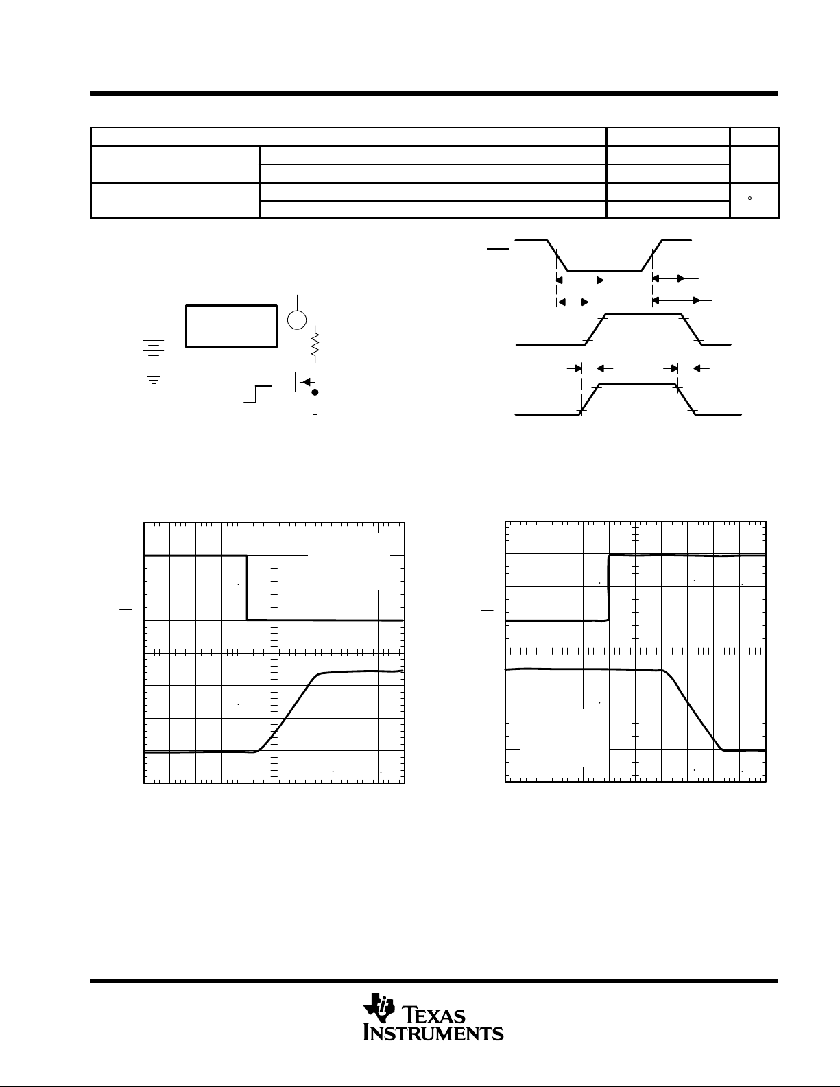
TEST CIRCUIT
Figure 1. Current Limit Response
V
I(EN)
(2 V/div)
Current
Meter
V
= 5 V
I(BP)
TA = 25°C
CL = 10 µF
RL = 50 Ω
V
I(ENx
V
O(OUTx)
V
O(OUTx)
)
t
pd(on)
t
on
50% 50%
10% 10%
t
r
10% 10%
TIMING
90% 90%
90% 90%
t
pd(off)
t
off
t
f
Figure 2. Timing and Internal Voltage Regulator
Transition Waveforms
V
I(EN)
(2 V/div)
V
O(out)
(2 V/div)
0 2 4 6 8 10 12 14 16 18 20
t – time – ms
Figure 3. Turnon Delay and Rise Time
(BP Switch)
V
O(OUT)
(2 V/div)
0 2 4 6 8 101214161820
Figure 4. Turnoff Delay and Fall Time
POST OFFICE BOX 655303 • DALLAS, TEXAS 75265
V
= 5 V
I(BP)
TA = 25°C
CL = 10 µF
RL = 50 Ω
t – time – ms
(BP Switch)
9
Page 10

TPS2074, TPS2075
FOUR-PORT USB HUB POWER CONTROLLERS
SLVS288A – SEPTEMBER 2000 – REVISED FEBRUARY 2001
PARAMETER MEASUREMENT INFORMATION
V
V
I(EN)
(2 V/div)
= V
I(BP)
TA = 25°C
CL = 10 µF
RL = 10 Ω
I(SP)
= 5 V
V
I(EN)
(2 V/div)
V
= V
I(BP)
TA = 25°C
CL = 10 µF
RL = 10 Ω
I(SP)
= 5 V
V
O(OUT)
(2 V/div)
V
I(BP)
(2 V/div)
V
3.3V_OUT)
(1 V/div)
V
O(out)
(2 V/div)
0 2 4 6 8 10 12 14 16 18 20 0 2 4 6 8 10 12 14 16 18 20
t – time – ms
Figure 5. Turnon Delay and Rise Time
(SP Switch)
TA = 25°C
CL = 4.7 µF
RL = 33 Ω
O
V
I(BP)
(2 V/div)
V
(3.3V_OUT)
(1 V/div)
Figure 6. Turnoff Delay and Fall Time
O
t – time – ms
(SP Switch)
TA = 25°C
CL = 4.7 µF
RL = 33 Ω
10
0 4 8 1216202428323640
t – time – ms
Figure 7. Turnon Delay and Rise Time
(3.3V_OUT)
POST OFFICE BOX 655303 • DALLAS, TEXAS 75265
0 20 40 60 80 100 120 140 160 180 200
t – time – ms
Figure 8. Turnoff Delay and Fall Time
(3.3V_OUT)
Page 11

PARAMETER MEASUREMENT INFORMATION
V
(3.3V_OUT)
(PG_DLY)
O
(2 V/div)
V
(2 V/div)
O
0
400
800
1200
V
I(BP)
TA = 25°C
C
L(PG_DLY)
1600
2000
t – time – ms
2400
= 5 V
2800
= 0.47 µF
3200
3600
4000
Figure 9. PG_DLY Rise Time With a 0.47-µF Capacitor
TPS2074, TPS2075
FOUR-PORT USB HUB POWER CONTROLLERS
SLVS288A – SEPTEMBER 2000 – REVISED FEBRUARY 2001
V
(2 V/div)
V
O(PG)
(2 V/div)
O
V
= 5 V
I(BP)
TA = 25°C
C
L(PG_DLY)
0 100 200 300 400 500 600 700 800 900 1000
t – time – ms
= 0.47 µF
Figure 10. Turnon Delay (3.3V_OUT to PG)
(3.3V_OUT)
V
(3.3V_OUT)
(2 V/div)
V
O(PG)
(2 V/div)
V
= 5 V
I(BP)
TA = 25°C
C
L(PG_DLY)
O
012345678910
t – time – ms
= 0.47 µF
Figure 11. Turnoff Time (3.3V_OUT to PG)
V
TA = 25°C
V
I(EN)
(2 V/div)
I
O(OUT)
(0.1A/div)
012345678910
t – time – ms
Figure 12. Short-Circuit Current (BP Switch),
Device Enabled Into Short
I(BP)
= 5 V
POST OFFICE BOX 655303 • DALLAS, TEXAS 75265
11
Page 12

TPS2074, TPS2075
FOUR-PORT USB HUB POWER CONTROLLERS
SLVS288A – SEPTEMBER 2000 – REVISED FEBRUARY 2001
PARAMETER MEASUREMENT INFORMATION
V
= V
I(BP)
TA = 25°C
I(SP)
= 5 V
V
= V
I(BP)
TA = 25°C
I(SP)
= 5 V
V
I(EN)
(2 V/div)
I
O(OUT)
(0.5 A/div)
012345678910
t – time – ms
Figure 13. Short-Circuit Current (SP Switch),
Device Enabled Into Short
V
= 5 V
I(BP)
TA = 25°C
V
O(OC)
(2 V/div)
V
O(OC)
(2 V/div)
I
O(OUT)
(0.5 A/div)
V
O(PG)
(2 V/div)
012345678910
t – time – ms
Figure 14. OC Response (SP Switch),
Device Enabled Into Short
V
= 5 V
I(BP)
TA = 25°C
BP_DIS = 0 V or Open
C
L(3.3 V_OUT)
R
L(3.3 V_OUT)
C
L(PG_DLY)
= 4.7 µF
= 33 Ω
= 0.47 µF
I
O(OUT)
(0.1 A/div)
12
(3.3V_OUT)
012345678910
t – time – ms
Figure 15. OC Response (BP Switch),
Device Enabled Into Short
POST OFFICE BOX 655303 • DALLAS, TEXAS 75265
V
(1 V/div)
O
0 2 4 6 8 10 12 14 16 18 20
t – time – ms
Figure 16. SP to BP Automatic
Switchover Enabled
Page 13

FOUR-PORT USB HUB POWER CONTROLLERS
SLVS288A – SEPTEMBER 2000 – REVISED FEBRUARY 2001
PARAMETER MEASUREMENT INFORMATION
V
= 5 V
V
= 5 V
I(BP)
TA = 25°C
BP_DIS = 5 V
I(BP)
TA = 25°C
BP_DIS = 0 V or Open
TPS2074, TPS2075
V
O(PG)
(2 V/div)
V
(3.3V_OUT)
(1 V/div)
V
O(PG)
(2 V/div)
O
012345678910
t – time – ms
Figure 17. SP to BP Automatic
Switchover Disabled
V
= 5 V
I(BP)
TA = 25°C
BP_DIS = 5 V
V
O(PG)
(2 V/div)
V
(DPO_RST)
(1 V/div)
5.25 V
V
I(BP)
4.25 V
O
0 40 80 120 160 200 240 280 320 360 400
t – time – ms
Figure 18. SP to BP Automatic
Switchover Enabled
V
(DPO_RST)
(1 V/div)
O
0 40 80 120 160 200 240 280 320 360 400
t – time – ms
Figure 19. SP to BP Automatic
Switchover Disabled
∆V
(3.3V_OUT)
(0.05 V/div)
O
TA = 25°C
CL (3.3 V–OUT) = 4.7 µF
IO (3.3 V–OUT) = 100 mA
0 100 200 300 400 500 600 700 800 900 1000
t – time – µs
Figure 20. Line Transient Response
POST OFFICE BOX 655303 • DALLAS, TEXAS 75265
13
Page 14

TPS2074, TPS2075
FOUR-PORT USB HUB POWER CONTROLLERS
SLVS288A – SEPTEMBER 2000 – REVISED FEBRUARY 2001
PARAMETER MEASUREMENT INFORMATION
TA = 25°C
CL
(3.3 V_OUT)
= 10 µF
196
194
I
O(3.3 V_OUT)
(100 mA/div)
(100 mV/div)
BP SUPPLY CURRENT
JUNCTION TEMPERATURE
V
= 5 V
I(BP)
∆V
(3.3 V_OUT)
vs
O
0 100 200 300 400 500 600 700 800 900
t – Time – µs
Figure 21. Load Transient Response
TYPICAL CHARACTERISTICS
205
200
1000
BP SUPPLY CURRENT
vs
INPUT VOLTAGE
14
192
Aµ
190
188
186
– Supply Current –
184
I(BP)
I
182
180
–60 –40 –20 0 20 40 60 80 100 120 140
Output Enabled
Output Disabled
TJ – Junction Temperature – °C
Figure 22
POST OFFICE BOX 655303 • DALLAS, TEXAS 75265
Aµ
195
190
185
180
– Supply Current –
I(BP)
175
I
170
165
4.25 4.5 4.75 5
Output Enabled
V
I(BP)
Figure 23
Output Disabled
5.25 5.5
– Input Voltage – V
Page 15

FOUR-PORT USB HUB POWER CONTROLLERS
SLVS288A – SEPTEMBER 2000 – REVISED FEBRUARY 2001
TYPICAL CHARACTERISTICS
TPS2074, TPS2075
SP SUPPLY CURRENT
vs
JUNCTION TEMPERATURE
120
V
= 5 V
I(SP)
115
A
µ
– Supply Current –
I(SP)
I
110
105
100
95
–60 –40 –20
Outputs Disabled
Outputs Enabled
20 40 60 80 100 120 140
0
TJ – Junction Temperature – °C
Figure 24
STATIC DRAIN-SOURCE ON-STATE RESISTANCE
vs
JUNCTION TEMPERATURE
Ω
200
180
160
140
120
(SELF-POWER SWITCHES)
V
= 5 V
I(SP)
SP SUPPLY CURRENT
vs
INPUT VOLTAGE
120
115
Aµ
Outputs Disabled
110
105
– Supply Current –
I(SP)
I
100
95
4.5 5
V
Outputs Enabled
– Input Voltage – V
I(SP)
Figure 25
STATIC DRAIN-SOURCE ON-STATE RESISTANCE
vs
JUNCTION TEMPERATURE
Ω
800
700
600
500
(BUS POWER SWITCHES)
V
= 5.5 V
I(BP)
5.5
100
80
60
40
– Static Drain-Source On-State Resistance –
20
0
DS(on)
r
–40 0 25
85 125
TJ – Junction Temperature – °C
Figure 26
POST OFFICE BOX 655303 • DALLAS, TEXAS 75265
400
300
200
– Static Drain-Source On-State Resistance –
100
0
DS(on)
r
–40 0 25
TJ – Junction Temperature – °C
V
= 4.25 V
I(BP)
Figure 27
85 125
15
Page 16

TPS2074, TPS2075
FOUR-PORT USB HUB POWER CONTROLLERS
SLVS288A – SEPTEMBER 2000 – REVISED FEBRUARY 2001
TYPICAL CHARACTERISTICS
SHORT-CIRCUIT OUTPUT CURRENT
vs
JUNCTION TEMPERATURE
(BUS-POWER SWITCHES)
300
V
= 4.25 V
I(BP)
–40 0 25 85 125
TJ – Junction Temperature – °C
– Short-Circuit Output Current – mA
OS
I
280
260
240
220
200
180
160
140
Figure 28
SHORT-CIRCUIT OUTPUT CURRENT
vs
JUNCTION TEMPERATURE
(BUS-POWER SWITCHES)
250
V
= 5.5 V
I(BP)
230
210
190
170
150
– Short-Circuit Output Current – mA
130
OS
I
110
–40 0 25 85 125
TJ – Junction Temperature – °C
Figure 29
SHORT-CIRCUIT OUTPUT CURRENT
vs
JUNCTION TEMPERATURE
(SELF-POWER SWITCHES)
– Short-Circuit Output Current – mA
OS
I
1000
V
= 5 V
980
960
940
920
900
880
860
840
820
800
I(SP)
–40 0 25 85 125
TJ – Junction Temperature – °C
Figure 30
INPUT VOLTAGE (BP UNDERVOLTAGE LOCKOUT)
vs
JUNCTION TEMPERATURE
4.25
4.2
4.15
4.1
4.05
4
3.95
3.9
3.85
– Input Voltage (BP Undervoltage Lockout) – V
3.8
I(BP)
3.75
V
–50 0 50
TJ – Junction Temperature – °C
Start Threshold
Stop Threshold
100 150
Figure 31
16
POST OFFICE BOX 655303 • DALLAS, TEXAS 75265
Page 17

FOUR-PORT USB HUB POWER CONTROLLERS
SLVS288A – SEPTEMBER 2000 – REVISED FEBRUARY 2001
TYPICAL CHARACTERISTICS
INPUT VOLTAGE (SP UNDERVOLTAGE LOCKOUT)
vs
JUNCTION TEMPERATURE
4.5
4.45
4.4
4.35
4.3
4.25
4.2
4.15
Start Threshold
TPS2074, TPS2075
4.1
– Input Voltage (SP Undervoltage Lockout) – V
4.05
I(SP)
4
V
–50 0 50
TJ – Junction Temperature – °C
Stop Threshold
100 150
Figure 32
APPLICATION INFORMATION
external capacitor requirements
A 0.1-µF ceramic bypass capacitor and a 10-µF bulk capacitor between BP and AGND, close to the device, are
recommended. Similarly , a 0.1-µF ceramic and a 68-µF bulk capacitor, from SP to AGND, and from VEXT to
AGND if an external 5-V LDO is required, are recommended because of much higher current in the self-powered
mode.
From each of the outputs (OUTx) to ground, a 33-µF or higher valued bulk capacitor is recommended when the
output load is heavy . This precaution reduces power-supply transients. Additionally, bypassing the outputs with
a 0.1-µF ceramic capacitor improves the immunity of the device to short-circuit transients.
An output capacitor connected between 3.3V_OUT and GND is required to stabilize the internal control loop.
The internal LDO is designed for a capacitor range of 4.7 µF to 33 µF with an ESR of 0.2 Ω to 10 Ω. Solid
tantalum-electrolytic, aluminum-electrolytic, and multilayer ceramic capacitors are all suitable.
Ceramic capacitors have different types of dielectric material, each exhibiting different temperature and voltage
variations. The most common types are X5R, X7R, Y5U, Z5U, and NPO. The NPO type ceramic capacitors are
generally the most stable over temperature. However, the X5R and X7R are also relatively stable over
temperature (with the X7R being the more stable of the two) and are therefore acceptable for use. The Y5U and
Z5U types provide high capacitance in a small geometry , but exhibit large variations over temperature. For this
reason, the Y5U and Z5U are not generally recommended.
POST OFFICE BOX 655303 • DALLAS, TEXAS 75265
17
Page 18

TPS2074, TPS2075
FOUR-PORT USB HUB POWER CONTROLLERS
SLVS288A – SEPTEMBER 2000 – REVISED FEBRUARY 2001
APPLICATION INFORMATION
external capacitor requirements (continued)
A transient condition occurs because of a sudden increase in output current. The output capacitor reduces the
transient effect by providing the additional current needed by the load. Depending on the current demand at the
output, a voltage drop will occur across the internal resistance, ESR, of the capacitor. Using a low ESR capacitor
will help minimize this voltage drop. A larger capacitor will also reduce the voltage drop by supplying the current
demand for a longer time, versus that provided by a smaller capacitor.
overcurrent
An internal sense FET checks for overcurrent conditions. Unlike current-sense resistors, sense FETs do not
increase the series resistance of the current path. When an overcurrent condition is detected, the device
maintains a constant output current and reduces the output voltage accordingly. Complete shutdown occurs
only if the fault is present long enough to activate thermal limiting.
Three possible overload conditions can occur. In the first condition, the output has been shorted before the
device is enabled or before BP and SP have been applied. The TPS2074 and TPS2075 sense the short and
immediately switch into a constant-current output.
In the second condition, the short occurs while the device is enabled. At the instant the short occurs, very high
currents may flow for a very short time before the current-limit circuit can react. After the current-limit circuit has
tripped (reached the overcurrent trip threshold), the device switches into constant-current mode.
In the third condition, the load has been gradually increased beyond the recommended operating current. The
current is permitted to rise until the current-limit threshold is reached or until the thermal limit of the device is
exceeded. The TPS2074 and TPS2075 are capable of delivering current up to the current-limit threshold without
damaging the device. Once the threshold has been reached, the device switches into its constant-current mode.
OC response
The OCx output is asserted (active low) when an overcurrent or overtemperature condition is encountered and
will remain asserted until the overcurrent or overtemperature condition is removed. Connecting a heavy
capacitive load to an enabled device can cause momentary false overcurrent reporting from the inrush current
flowing through the device and charging the downstream capacitor. The TPS2074 and TPS2075 are designed
to reduce false overcurrent reporting by implementing an internal deglitch circuit. This circuit eliminates the need
for an external filter, which requires extra components. Also, using low-ESR electrolytic capacitors on the
outputs can reduce erroneous overcurrent reporting by providing a low-impedance energy source to lower the
inrush current flow through the device during hot-plug events. The OCx
requiring no pullup or pulldown resistors.
outputs are logic outputs thereby
18
POST OFFICE BOX 655303 • DALLAS, TEXAS 75265
Page 19

TPS2074, TPS2075
FOUR-PORT USB HUB POWER CONTROLLERS
SLVS288A – SEPTEMBER 2000 – REVISED FEBRUARY 2001
APPLICATION INFORMATION
power dissipation and junction temperature
The major source of power dissipation for the TPS2074 and TPS2075 comes from the internal voltage regulator
and the N-channel MOSFETs. Checking the power dissipation and junction temperature is always a good
design practice. Begin by determining the r
operating temperature. As an initial estimate, use the highest operating ambient temperature of interest and
read r
the power dissipation per switch can be calculated by:
Multiply this number by four to get the total power dissipation coming from the N-channel MOSFETs.
The power dissipation for the internal voltage regulator is calculated using:
from the graphs shown under the typical characteristics section of this data sheet. Using this value,
DS(on)
+
r
P
D
DS(on)
2
I
of the N-channel MOSFET according to the input voltage and
DS(on)
)
Ǔ
I
O(OUT)
)ǒ4 P
T
A
D(switch)
Ǔ
P
+ǒV
D
The total power dissipation for the device becomes:
P
D(total)
Finally, calculate the junction temperature:
+
PD
T
J
Where:
T
= ambient temperature °C
A
R
= Thermal resistance °C /W, equal to inverting of derating factor found on the power dissipation
θJA
Compare the calculated junction temperature with the initial estimate. If they do not agree within a few degrees,
repeat the calculation, using the calculated value as the new estimate. Two or three iterations are generally
sufficient to get a reasonable answer.
–V
I(BP)
+
table in this data sheet.
O(min)
P
D(voltage regulator)
R
q
JA
thermal protection
Thermal protection prevents damage to the IC when heavy-overload or short-circuit faults are present for
extended periods. The faults force the TPS2074 and TPS2075 into constant-current mode at first, which causes
the voltage across the high-side switch to increase; under short-circuit conditions, the voltage across the switch
is equal to the input voltage. The increased dissipation causes the junction temperature to rise to high levels.
The protection circuit senses the junction temperature of the switch and shuts it off. Hysteresis is built into the
thermal sense circuit, and after the device has cooled approximately 20 degrees the switch turns back on. The
switch continues to cycle in this manner until the load fault or input power is removed.
The TPS2074 and TPS2075 implement a dual thermal trip to allow fully independent operation of the power
distribution switches. In an overcurrent or short-circuit condition the junction temperature rises. Once the die
temperature rises to approximately 140°C, the internal thermal-sense circuitry determines which power switch
is in an overcurrent condition and turns only that power switch off, thus isolating the fault without interrupting
operation of the adjacent power switch. If the die temperature exceeds the first thermal trip point of 140°C and
reaches 150°C, the device turns off. The OC
overcurrent occurs.
POST OFFICE BOX 655303 • DALLAS, TEXAS 75265
output is asserted (active low) when overtemperature or
19
Page 20

TPS2074, TPS2075
FOUR-PORT USB HUB POWER CONTROLLERS
SLVS288A – SEPTEMBER 2000 – REVISED FEBRUARY 2001
APPLICATION INFORMATION
undervoltage lockout (UVLO)
An undervoltage lockout ensures that the device (LDO and switches) is in the off state at power up. The UVLO
will also keep the device from being turned on until the power supply has reached the start threshold (see
undervoltage lockout table), even if the switches are enabled. The UVLO will activate whenever the input
voltage falls below the stop threshold as defined in the undervoltage lockout table. This facilitates the design
of hot-insertion systems where it is not possible to turn off the power switches before input power is removed.
Upon reinsertion, the power switches will be turned on with a controlled rise time to reduce EMI and voltage
overshoots.
self-power to bus-power or bus-power to self-power transition
An autoswitching function between bus-powered mode and self-powered mode is a feature of the TPS2074 and
TPS2075. When this feature is enabled (BP_DIS is inactive) and SP is removed or applied, a transition will be
initiated. The transition sequence begins with the internal LDO being turned off and its external capacitance
discharged. Any enabled switches are also turned off and the external capacitors discharged. Once the LDO
and switch outputs are low, the internal logic will turn the LDO back on. This entire sequence occurs whenever
power to the SP input is removed or applied, regardless of the source of power, i.e., an external power supply
or the use of the external regulator.
universal serial bus (USB) applications
The universal serial bus (USB 1.1) interface is a 12-Mb/s, 1.5-Mb/s, or 480 Mb/s (USB 2.0), multiplexed serial
bus designed for low-to-medium bandwidth PC peripherals (e.g., keyboards, printers, scanners, and mice). The
four-wire USB interface is conceived for dynamic attach-detach (hot plug-unplug) of peripherals. Two lines are
provided for differential data, and two lines are provided for 5-V power distribution.
USB data is a 3.3-V-level signal, but power is distributed at 5 V to allow for voltage drops in cases where power
is distributed through more than one hub or across long cables. Each function must provide its own regulated
3.3 V from the 5-V input or its own internal power supply.
The USB specification defines the following five classes of devices, each differentiated by power-consumption
requirements:
D
Hosts/self-powered hubs (SPH)
D
Bus-powered hubs (BPH)
D
Low-power, bus-powered functions
D
High-power, bus-powered functions
D
Self-powered functions
Self-powered and bus-powered hubs distribute data and power to downstream functions. The TPS2074 and
TPS2075 can provide power-distribution solutions for hybrid hubs that need switching between BPH and SPH
according to power availability and application requirements.
20
POST OFFICE BOX 655303 • DALLAS, TEXAS 75265
Page 21

TPS2074, TPS2075
FOUR-PORT USB HUB POWER CONTROLLERS
SLVS288A – SEPTEMBER 2000 – REVISED FEBRUARY 2001
APPLICATION INFORMATION
USB power-distribution requirements
USB can be implemented in several ways, and, regardless of the type of USB device being developed, several
power-distribution features must be implemented.
D
Hosts/self-powered hubs must:
– Current-limit downstream ports
– Report overcurrent conditions on USB V
– Output 5.25 V to 4.75 at 500 mA
D
Bus-powered hubs must:
– Enable/disable power to downstream ports
– Power up at <100 mA
– Limit inrush current (<44 Ω and 10 µF)
– Output 5.25 V to 4.4 at 100 mA
– Not send power back upstream
D
Functions must:
BUS
– Limit inrush currents
– Power up at <100 mA
– Not send power back upstream (SP functions)
The feature set of the TPS2074 and TPS2075 allows them to meet each of these requirements. The integrated
current-limiting and overcurrent reporting is required by hosts and self-powered hubs. The logic-level enable
and controlled rise times meet the needs of both input and output ports on hubs, as well as the input ports for
bus-powered functions
USB hybrid hub
A USB hybrid hub can be simply implemented using the TPS2075 USB power controller and a TUSB2046 USB
hub controller as shown in Figure 33. The TPS2075 USB power controller provides all the power needs to the
four downstream ports and meets all the USB power specifications for both self-powered hubs and bus-powered
hubs. The power controllers integrated 3.3-V LDO is used to provide power for the hub controller and any other
local functions (e.g. transient suppressor SN75240 ), which saves board space and cost. The TPS2075 also
provides the hub controller with a power good (PG) signal that connects to the RESET
to automatically reinitialize the hub when switching between self-powered mode and bus-powered mode
whenever the self-power supply is connected or disconnected. The amount of time in which the hub controller
is kept in a reset state is controlled by a capacitor connected between the PG_DL Y pin of the power controller
and ground.
input of the hub controller
POST OFFICE BOX 655303 • DALLAS, TEXAS 75265
21
Page 22

TPS2074, TPS2075
FOUR-PORT USB HUB POWER CONTROLLERS
SLVS288A – SEPTEMBER 2000 – REVISED FEBRUARY 2001
APPLICATION INFORMATION
Upstream
Ports
D+
D–
GND
5 V
0.1 µF
10 µF
SN75240
CDA
B
33 pF
0.1 µF
33 pF
6 MHz
1.5 kΩ
TUSB2046B
DP0
DM0
EECLK
EEDATA
EXTMEM
SUSPEND
BUSPWR
RESET
VCC1_3.3
VCC2_3.3
XTAL1
XTAL2
TSTPLL
TSTMODE
GND
GND
DP1
DM1
DP2
DM2
DP3
DM3
DP4
DM4
PWRON1
OVRCUR1
PWRON2
OVRCUR2
PWRON3
OVRCUR3
PWRON4
OVRCUR4
SN75240
SN75240
EN1
OC1
EN2
OC2
EN3
OC3
EN4
OC4
CDA
B
CDA
B
TPS2075
OUT1
OUT2
OUT3
OUT4
Downstream
Ports
D+
D–
GND
5 V
33 µF
D+
D–
GND
5 V
33 µF
D+
D–
GND
5 V
33 µF
D+
D–
GND
5 V
33 µF
0.1 µF
4.7 µF 0.1 µF
1.5 kΩ
5 V Power
Supply
3.3 V
SP
SP
0.1 µF68 µF
PG
BPMODE
DP0_RST
BP
BP_DIS
PG_DLY
AGND
DGND
Figure 33. USB Hybrid Hub Using TPS2075 Power Controller and TUSB2046 Hub Controller
22
POST OFFICE BOX 655303 • DALLAS, TEXAS 75265
Page 23

TPS2074, TPS2075
FOUR-PORT USB HUB POWER CONTROLLERS
SLVS288A – SEPTEMBER 2000 – REVISED FEBRUARY 2001
MECHANICAL DATA
DB (R-PDSO-G**) PLASTIC SMALL-OUTLINE PACKAGE
28 PINS SHOWN
0,65
28
1
2,00 MAX
0,38
0,22
15
14
A
0,05 MIN
0,15
5,60
5,00
M
8,20
7,40
Seating Plane
0,10
0,15 NOM
Gage Plane
0°–8°
0,25
1,03
0,63
PINS **
DIM
A MAX
A MIN
NOTES: A. All linear dimensions are in millimeters.
B. This drawing is subject to change without notice.
C. Body dimensions do not include mold flash or protrusion not to exceed 0,15.
D. Falls within JEDEC MO-150
8
3,30
2,70
14
6,50
6,50
5,905,90
2016
7,50
6,90
24
8,50
28
10,50
9,907,90
30
10,50
9,90
38
12,90
12,30
4040065 /C 10/95
POST OFFICE BOX 655303 • DALLAS, TEXAS 75265
23
Page 24

PACKAGE OPTION ADDENDUM
www.ti.com
6-Dec-2006
PACKAGING INFORMATION
Orderable Device Status
(1)
Package
Type
Package
Drawing
Pins Package
Qty
Eco Plan
TPS2074DB ACTIVE SSOP DB 24 60 Green (RoHS &
no Sb/Br)
TPS2074DBG4 ACTIVE SSOP DB 24 60 Green (RoHS &
no Sb/Br)
TPS2075DB ACTIVE SSOP DB 24 60 Green (RoHS &
no Sb/Br)
TPS2075DBG4 ACTIVE SSOP DB 24 60 Green (RoHS &
no Sb/Br)
TPS2075DBR ACTIVE SSOP DB 24 2000 Green (RoHS &
no Sb/Br)
TPS2075DBRG4 ACTIVE SSOP DB 24 2000 Green (RoHS &
no Sb/Br)
(1)
The marketing status values are defined as follows:
ACTIVE: Product device recommended for new designs.
LIFEBUY: TI has announced that the device will be discontinued, and a lifetime-buy period is in effect.
NRND: Not recommended for new designs. Device is in production to support existing customers, but TI does not recommend using this part in
a new design.
PREVIEW: Device has been announced but is not in production. Samples may or may not be available.
OBSOLETE: TI has discontinued the production of the device.
(2)
Lead/Ball Finish MSL Peak Temp
CU NIPDAU Level-1-260C-UNLIM
CU NIPDAU Level-1-260C-UNLIM
CU NIPDAU Level-1-260C-UNLIM
CU NIPDAU Level-1-260C-UNLIM
CU NIPDAU Level-1-260C-UNLIM
CU NIPDAU Level-1-260C-UNLIM
(3)
(2)
Eco Plan - The planned eco-friendly classification: Pb-Free (RoHS), Pb-Free (RoHS Exempt), or Green (RoHS & no Sb/Br) - please check
http://www.ti.com/productcontent for the latest availability information and additional product content details.
TBD: The Pb-Free/Green conversion plan has not been defined.
Pb-Free (RoHS): TI's terms "Lead-Free" or "Pb-Free" mean semiconductor products that are compatible with the current RoHS requirements
for all 6 substances, including the requirement that lead not exceed 0.1% by weight in homogeneous materials. Where designed to be soldered
at high temperatures, TI Pb-Free products are suitable for use in specified lead-free processes.
Pb-Free (RoHS Exempt): This component has a RoHS exemption for either 1) lead-based flip-chip solder bumps used between the die and
package, or 2) lead-based die adhesive used between the die and leadframe. The component is otherwise considered Pb-Free (RoHS
compatible) as defined above.
Green (RoHS & no Sb/Br): TI defines "Green" to mean Pb-Free (RoHS compatible), and free of Bromine (Br) and Antimony (Sb) based flame
retardants (Br or Sb do not exceed 0.1% by weight in homogeneous material)
(3)
MSL, Peak Temp. -- The Moisture Sensitivity Level rating according to the JEDEC industry standard classifications, and peak solder
temperature.
Important Information and Disclaimer:The information provided on this page represents TI's knowledge and belief as of the date that it is
provided. TI bases its knowledge and belief on information provided by third parties, and makes no representation or warranty as to the
accuracy of such information. Efforts are underway to better integrate information from third parties. TI has taken and continues to take
reasonable steps to provide representative and accurate information but may not have conducted destructive testing or chemical analysis on
incoming materials and chemicals. TI and TI suppliers consider certain information to be proprietary, and thus CAS numbers and other limited
information may not be available for release.
In no event shall TI's liability arising out of such information exceed the total purchase price of the TI part(s) at issue in this document sold by TI
to Customer on an annual basis.
Addendum-Page 1
Page 25

PACKAGE MATERIALS INFORMATION
www.ti.com
TAPE AND REEL INFORMATION
11-Mar-2008
*All dimensions are nominal
Device Package
Type
TPS2075DBR SSOP DB 24 2000 330.0 16.4 8.2 8.8 2.5 12.0 16.0 Q1
Package
Drawing
Pins SPQ Reel
Diameter
(mm)
Reel
Width
W1 (mm)
A0 (mm) B0 (mm) K0 (mm) P1
(mm)W(mm)
Pin1
Quadrant
Pack Materials-Page 1
Page 26

PACKAGE MATERIALS INFORMATION
www.ti.com
11-Mar-2008
*All dimensions are nominal
Device Package Type Package Drawing Pins SPQ Length (mm) Width (mm) Height (mm)
TPS2075DBR SSOP DB 24 2000 346.0 346.0 33.0
Pack Materials-Page 2
Page 27

IMPORTANT NOTICE
Texas Instruments Incorporated and its subsidiaries (TI) reserve the right to make corrections, modifications, enhancements, improvements,
and other changes to its products and services at any time and to discontinue any product or service without notice. Customers should
obtain the latest relevant information before placing orders and should verify that such information is current and complete. All products are
sold subject to TI’s terms and conditions of sale supplied at the time of order acknowledgment.
TI warrants performance of its hardware products to the specifications applicable at the time of sale in accordance with TI’s standard
warranty. Testing and other quality control techniques are used to the extent TI deems necessary to support this warranty. Except where
mandated by government requirements, testing of all parameters of each product is not necessarily performed.
TI assumes no liability for applications assistance or customer product design. Customers are responsible for their products and
applications using TI components. To minimize the risks associated with customer products and applications, customers should provide
adequate design and operating safeguards.
TI does not warrant or represent that any license, either express or implied, is granted under any TI patent right, copyright, mask work right,
or other TI intellectual property right relating to any combination, machine, or process in which TI products or services are used. Information
published by TI regarding third-party products or services does not constitute a license from TI to use such products or services or a
warranty or endorsement thereof. Use of such information may require a license from a third party under the patents or other intellectual
property of the third party, or a license from TI under the patents or other intellectual property of TI.
Reproduction of TI information in TI data books or data sheets is permissible only if reproduction is without alteration and is accompanied
by all associated warranties, conditions, limitations, and notices. Reproduction of this information with alteration is an unfair and deceptive
business practice. TI is not responsible or liable for such altered documentation. Information of third parties may be subject to additional
restrictions.
Resale of TI products or services with statements different from or beyond the parameters stated by TI for that product or service voids all
express and any implied warranties for the associated TI product or service and is an unfair and deceptive business practice. TI is not
responsible or liable for any such statements.
TI products are not authorized for use in safety-critical applications (such as life support) where a failure of the TI product would reasonably
be expected to cause severe personal injury or death, unless officers of the parties have executed an agreement specifically governing
such use. Buyers represent that they have all necessary expertise in the safety and regulatory ramifications of their applications, and
acknowledge and agree that they are solely responsible for all legal, regulatory and safety-related requirements concerning their products
and any use of TI products in such safety-critical applications, notwithstanding any applications-related information or support that may be
provided by TI. Further, Buyers must fully indemnify TI and its representatives against any damages arising out of the use of TI products in
such safety-critical applications.
TI products are neither designed nor intended for use in military/aerospace applications or environments unless the TI products are
specifically designated by TI as military-grade or "enhanced plastic." Only products designated by TI as military-grade meet military
specifications. Buyers acknowledge and agree that any such use of TI products which TI has not designated as military-grade is solely at
the Buyer's risk, and that they are solely responsible for compliance with all legal and regulatory requirements in connection with such use.
TI products are neither designed nor intended for use in automotive applications or environments unless the specific TI products are
designated by TI as compliant with ISO/TS 16949 requirements. Buyers acknowledge and agree that, if they use any non-designated
products in automotive applications, TI will not be responsible for any failure to meet such requirements.
Following are URLs where you can obtain information on other Texas Instruments products and application solutions:
Products Applications
Amplifiers amplifier.ti.com Audio www.ti.com/audio
Data Converters dataconverter.ti.com Automotive www.ti.com/automotive
DSP dsp.ti.com Broadband www.ti.com/broadband
Clocks and Timers www.ti.com/clocks Digital Control www.ti.com/digitalcontrol
Interface interface.ti.com Medical www.ti.com/medical
Logic logic.ti.com Military www.ti.com/military
Power Mgmt power.ti.com Optical Networking www.ti.com/opticalnetwork
Microcontrollers microcontroller.ti.com Security www.ti.com/security
RFID www.ti-rfid.com Telephony www.ti.com/telephony
RF/IF and ZigBee® Solutions www.ti.com/lprf Video & Imaging www.ti.com/video
Mailing Address: Texas Instruments, Post Office Box 655303, Dallas, Texas 75265
Copyright © 2008, Texas Instruments Incorporated
Wireless www.ti.com/wireless
 Loading...