

Page 1
TPS1120, TPS1120Y
DUAL P-CHANNEL ENHANCEMENT-MODE MOSFETS
SLVS080A – MARCH 1994 – REVISED AUGUST 1995
1
POST OFFICE BOX 655303 • DALLAS, TEXAS 75265
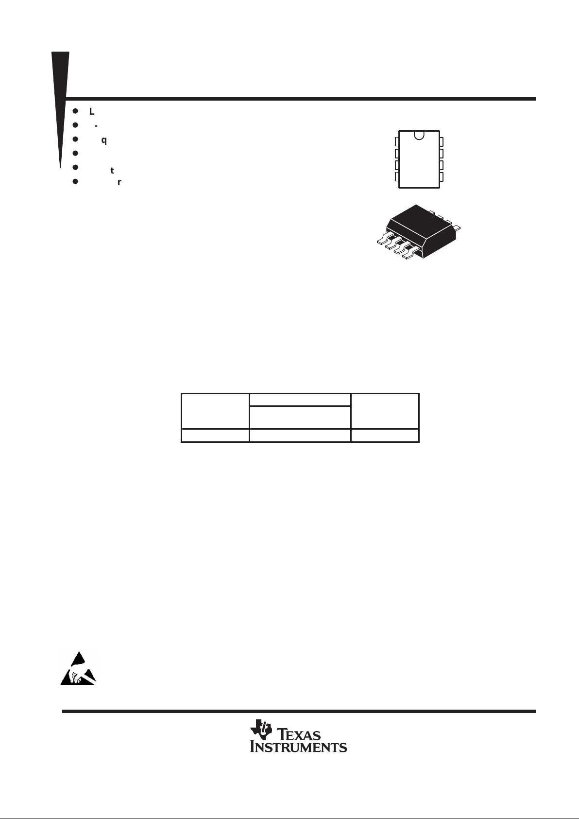
D
Low r
DS(on)
. . . 0.18 Ω at VGS = –10 V
D
3-V Compatible
D
Requires No External V
CC
D
TTL and CMOS Compatible Inputs
D
V
GS(th)
= –1.5 V Max
D
ESD Protection Up to 2 kV per
MIL-STD-883C, Method 3015
description
The TPS1120 incorporates two independent
p-channel enhancement-mode MOSFETs that
have been optimized, by means of the Texas
Instruments LinBiCMOS process, for 3-V or 5-V
power distribution in battery-powered systems. With a maximum V
GS(th)
of –1.5 V and an I
DSS
of only 0.5 µA,
the TPS1120 is the ideal high-side switch for low-voltage portable battery-management systems, where
maximizing battery life is a primary concern. Because portable equipment is potentially subject to electrostatic
discharge (ESD), the MOSFET s have built-in circuitry for 2-kV ESD protection. End equipment for the TPS1 120
includes notebook computers, personal digital assistants (PDAs), cellular telephones, bar-code scanners, and
PCMCIA cards. For existing designs, the TPS1 120D has a pinout common with other p-channel MOSFETs in
small-outline integrated circuit SOIC packages.
The TPS1120 is characterized for an operating junction temperature range, T
J
, from –40°C to 150°C.
AVAILABLE OPTIONS
PACKAGED DEVICES
†
T
J
SMALL OUTLINE
(D)
CHIP FORM
(Y)
–40°C to 150°C TPS1120D TPS1120Y
†
The D package is available taped and reeled. Add an R suffix to device
type (e.g., TPS1120DR). The chip form is tested at 25°C.
Caution. This device contains circuits to protect its inputs and outputs against damage due to high static voltages or electrostatic
fields. These circuits have been qualified to protect this device against electrostatic discharges (ESD) of up to 2 kV according to
MIL-STD-883C, Method 3015; however, it is advised that precautions be taken to avoid application of any voltage higher than
maximum-rated voltages to these high-impedance circuits.
LinBiCMS is a trademark of Texas Instruments Incorporated.
Copyright 1995, Texas Instruments Incorporated
PRODUCTION DATA information is current as of publication date.
Products conform to specifications per the terms of Texas Instruments
standard warranty. Production processing does not necessarily include
testing of all parameters.
1
2
3
4
8
7
6
5
1SOURCE
1GATE
2SOURCE
2GATE
1DRAIN
1DRAIN
2DRAIN
2DRAIN
D PACKAGE
(TOP VIEW)
Page 2
TPS1120, TPS1120Y
DUAL P-CHANNEL ENHANCEMENT-MODE MOSFETS
SLVS080A – MARCH 1994 – REVISED AUGUST 1995
2
POST OFFICE BOX 655303 • DALLAS, TEXAS 75265
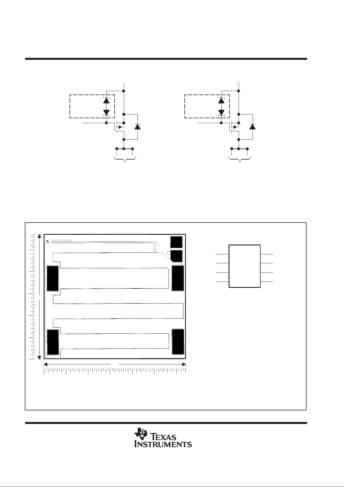
schematic
1GATE
1SOURCE
1DRAIN
†
ESD-
Protection
Circuitry
2GATE
2SOURCE
2DRAIN
†
ESD-
Protection
Circuitry
†
For all applications, both drain pins for each device should be connected.
TPS1120Y chip information
This chip, when properly assembled, displays characteristics similar to the TPS1 120C. Thermal compression
or ultrasonic bonding may be used on the doped aluminum bonding pads. The chip may be mounted with
conductive epoxy or a gold-silicon preform.
BONDING PAD ASSIGNMENTS
CHIP THICKNESS: 15 MILS TYPICAL
BONDING PADS: 4 × 4 MILS MINIMUM
TJmax = 150°C
TOLERANCES ARE ±10%
ALL DIMENSIONS ARE IN MILS
TPS1120Y
(2)
(6)
(1)
(3)
(7)
(8)
(5)(4)
1DRAIN1SOURCE
1GATE
2SOURCE
2GATE
1DRAIN
2DRAIN
2DRAIN
57
64
(2)
(1)
(3)
(4)
(6)
(7)
(8)
(5)
Page 3
TPS1120, TPS1120Y
DUAL P-CHANNEL ENHANCEMENT-MODE MOSFETS
SLVS080A – MARCH 1994 – REVISED AUGUST 1995
3
POST OFFICE BOX 655303 • DALLAS, TEXAS 75265
absolute maximum ratings over operating free-air temperature (unless otherwise noted)
†
UNIT
Drain-to-source voltage, V
DS
–15 V
Gate-to-source voltage, V
GS
2 or –15 V
TA = 25°C ±0.39
V
GS
= –2.7
V
TA = 125°C ±0.21
TA = 25°C ±0.5
°
V
GS
= –3
V
TA = 125°C ±0.25
Continuous drain current, each device (T
J
=
150°C), I
D
TA = 25°C ±0.74
A
V
GS
= –4.5
V
TA = 125°C ±0.34
TA = 25°C ±1.17
V
GS
= –10
V
TA = 125°C ±0.53
Pulse drain current, I
D
TA = 25°C ±7 A
Continuous source current (diode conduction), I
S
TA = 25°C –1 A
Continuous total power dissipation See Dissipation Rating Table
Storage temperature range, T
stg
–55 to 150 °C
Operating junction temperature range, T
J
–40 to 150 °C
Operating free-air temperature range, T
A
–40 to 125 °C
Lead temperature 1,6 mm (1/16 inch) from case for 10 seconds 260 °C
†
Stresses beyond those listed under “absolute maximum ratings” may cause permanent damage to the device. These are stress ratings only, and
functional operation of the device at these or any other conditions beyond those indicated under “recommended operating conditions” is not
implied. Exposure to absolute-maximum-rated conditions for extended periods may affect device reliability.
DISSIPATION RATING TABLE
PACKAGE
TA ≤ 25°C
POWER RATING
DERATING FACTOR
‡
ABOVE TA = 25°C
TA = 70°C
POWER RATING
TA = 85°C
POWER RATING
TA = 125°C
POWER RATING
D 840 mW 6.71 mW/°C 538 mW 437 mW 169 mW
‡
Maximum values are calculated using a derating factor based on R
θJA
= 149°C/W for the package. These devices are
mounted on an FR4 board with no special thermal considerations.
Page 4
TPS1120, TPS1120Y
DUAL P-CHANNEL ENHANCEMENT-MODE MOSFETS
SLVS080A – MARCH 1994 – REVISED AUGUST 1995
4
POST OFFICE BOX 655303 • DALLAS, TEXAS 75265
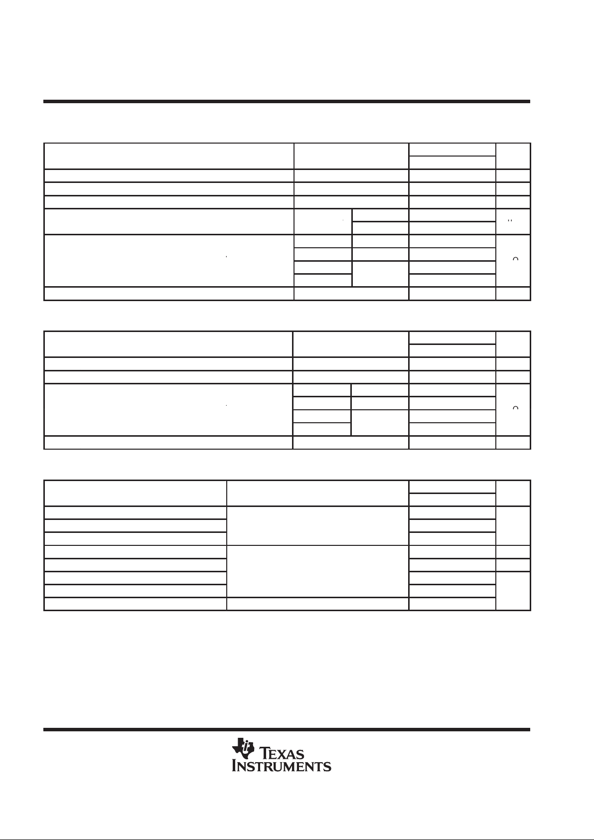
electrical characteristics at TJ = 25°C (unless otherwise noted)
static
TPS1120
PARAMETER
TEST CONDITIONS
MIN TYP MAX
UNIT
V
GS(th)
Gate-to-source threshold voltage VDS = VGS, ID = –250 µA –1 –1.25 –1.50 V
V
SD
Source-to-drain voltage (diode forward voltage)
†
IS = –1 A, VGS = 0 V –0.9 V
I
GSS
Reverse gate current, drain short circuited to source VDS = 0 V, VGS = –12 V ±100 nA
V
= –12 V ,
TJ = 25°C –0.5
I
DSS
Zero-gate-voltage drain current
DS
,
VGS = 0 V
TJ = 125°C –10
µ
A
VGS = –10 V ID = –1.5 A 180
VGS = –4.5 V ID = –0.5 A 291 400
r
DS(on)
Static drain-t
o-source on-state resistance
†
VGS = –3 V
476 700
mΩ
VGS = –2.7 V
I
D
= –0.2
A
606 850
g
fs
Forward transconductance
†
VDS = –10 V , ID = –2 A 2.5 S
†
Pulse test: pulse width ≤ 300 µs, duty cycle ≤ 2%
static
TPS1120Y
PARAMETER
TEST CONDITIONS
MIN TYP MAX
UNIT
V
GS(th)
Gate-to-source threshold voltage VDS = VGS, ID = –250 µA –1.25 V
V
SD
Source-to-drain voltage (diode forward voltage)
†
IS = –1 A, VGS = 0 V –0.9 V
VGS = –10 V ID = –1.5 A 180
VGS = –4.5 V ID = –0.5 A 291
r
DS(on)
Static drain-t
o-source on-state resistance
†
VGS = –3 V
476
mΩ
VGS = –2.7 V
I
D
= –0.2
A
606
g
fs
Forward transconductance
†
VDS = –10 V , ID = –2 A 2.5 S
†
Pulse test: pulse width ≤ 300 µs, duty cycle ≤ 2%
dynamic
TPS1120, TPS1120Y
PARAMETER
TEST CONDITIONS
MIN TYP MAX
UNIT
Q
g
Total gate charge 5.45
Q
gs
Gate-to-source charge
VDS = –10 V , VGS = –10 V , ID = –1 A
0.87
nC
Q
gd
Gate-to-drain charge 1.4
t
d(on)
Turn-on delay time 4.5 ns
t
d(off)
Turn-off delay time
V
= –10 V , R
= 10 Ω,I
= –1 A,
13 ns
t
r
Rise time
DD
,
RG = 6 Ω,
L
,
See Figures 1 and 2
D
,
10
t
f
Fall time 2
ns
t
rr(SD)
Source-to-drain reverse recovery time IF = 5.3 A, di/dt = 100 A/µs 16
Page 5

TPS1120, TPS1120Y
DUAL P-CHANNEL ENHANCEMENT-MODE MOSFETS
SLVS080A – MARCH 1994 – REVISED AUGUST 1995
5
POST OFFICE BOX 655303 • DALLAS, TEXAS 75265
PARAMETER MEASUREMENT INFORMATION
Figure 1. Switching-Time Test Circuit
R
G
R
L
V
DD
–
+
V
GS
DUT
V
DS
Figure 2. Switching-Time Waveforms
t
d(on)
t
r
V
DS
t
d(off)
t
f
90%
10%
0 V
–10 V
V
GS
Page 6

TPS1120, TPS1120Y
DUAL P-CHANNEL ENHANCEMENT-MODE MOSFETS
SLVS080A – MARCH 1994 – REVISED AUGUST 1995
6
POST OFFICE BOX 655303 • DALLAS, TEXAS 75265
TYPICAL CHARACTERISTICS
†
Table of Graphs
FIGURE
Drain current vs Drain-to-source voltage 3
Drain current vs Gate-to-source voltage 4
Static drain-to-source on-state resistance vs Drain current 5
Capacitance vs Drain-to-source voltage 6
Static drain-to-source on-state resistance (normalized) vs Junction temperature 7
Source-to-drain diode current vs Source-to-drain voltage 8
Static drain-to-source on-state resistance vs Gate-to-source voltage 9
Gate-to-source threshold voltage vs Junction temperature 10
Gate-to-source voltage vs Gate charge 11
– 5
– 4
– 2
– 1
0
– 3
0 – 1– 2– 3– 4– 5– 6
– Drain Current – A
– 7
– 6
DRAIN CURRENT
vs
DRAIN-TO-SOURCE VOLTAGE
– 7 – 8 – 9 – 10
VGS = –6 V
I
D
VDS – Drain-to-Source Voltage – V
VGS = –8 V
VGS = –7 V
VGS = –3 V
VGS = –4 V
VGS = –2 V
VGS = –5 V
TJ = 25°C
Figure 3 Figure 4
0 – 2 – 3 – 5
DRAIN CURRENT
vs
GATE-TO-SOURCE VOLTAGE
– 7– 1 – 4 – 6
– Drain Current – A
I
D
VGS – Gate-to-Source Voltage – V
TJ = 150°C
TJ = 25°C
TJ = –40°C
VDS = –10 V
0
– 5
– 4
– 2
– 1
– 3
– 7
– 6
†
All characteristics data applies for each independent MOSFET incorporated on the TPS1120.
Page 7

TPS1120, TPS1120Y
DUAL P-CHANNEL ENHANCEMENT-MODE MOSFETS
SLVS080A – MARCH 1994 – REVISED AUGUST 1995
7
POST OFFICE BOX 655303 • DALLAS, TEXAS 75265
TYPICAL CHARACTERISTICS
0.3
0.2
0.1
0
– 0.1 – 1
0.4
0.5
STATIC DRAIN-TO-SOURCE ON-STATE RESISTANCE
vs
DRAIN CURRENT
0.6
– 10
ID – Drain Current – A
0.7
VGS = –2.7 V
VGS = –3 V
VGS = –4.5 V
VGS = –10 V
TJ = 25°C
– Static Drain-to-Source
r
DS(on)
ΩOn-State Resistance –
Figure 5
200
150
50
0
0 – 1 – 2 – 3 – 4 – 5 – 6
C – Capacitance – pF
250
300
CAPACITANCE
vs
DRAIN-TO-SOURCE VOLTAGE
350
– 7 – 8 – 9 –12
100
–10 –11
C
oss
VDS – Drain-to-Source Voltage – V
C
iss
†
C
rss
‡
VGS = 0
f = 1 MHz
TJ = 25°C
†
C
rss
+
Cgd,C
oss
+
Cds)
CgsC
gd
Cgs)
C
gd
≈ Cds)
C
gd
‡
C
iss
+
Cgs)
Cgd,C
ds(shorted)
Figure 6
Figure 7
1.2
0.9
0.8
0.6
1.3
1.4
STATIC DRAIN-TO-SOURCE
ON-STATE RESISTANCE (NORMALIZED)
vs
JUNCTION TEMPERATURE
1.5
1.1
1
0.7
–50 0 50 100 150
TJ – Junction Temperature – °C
VGS = –10 V
ID = –1A
– Static Drain-to-Source
r
DS(on)
On-State Resistance (Normalized)
– 0.1
0 – 0.6 –1.2 –1.8
– Source-to-Drain Diode Current – A
SOURCE-TO-DRAIN DIODE CURRENT
vs
SOURCE-TO-DRAIN VOLTAGE
–1
–10
– 0.2 – 0.4 – 0.8 – 1 –1.4 –1.6
I
SD
VSD – Source-to-Drain Voltage – V
Pulse Test
TJ = 150°C
TJ = 25°C
TJ = –40°C
Figure 8
Page 8

TPS1120, TPS1120Y
DUAL P-CHANNEL ENHANCEMENT-MODE MOSFETS
SLVS080A – MARCH 1994 – REVISED AUGUST 1995
8
POST OFFICE BOX 655303 • DALLAS, TEXAS 75265
TYPICAL CHARACTERISTICS
0.2
0.1
0
– 1 – 3 – 5 – 7
0.3
0.4
STATIC DRAIN-TO-SOURCE ON-STATE RESISTANCE
vs
GATE-TO-SOURCE VOLTAGE
0.5
– 9 – 11
– 13 – 15
VGS – Gate-to-Source Voltage – V
0.6
0.7
ID = –1 A
TJ = 25°C
– Static Drain-to-Source On-State
r
DS(on)
Ω
Resistance –
Figure 9 Figure 10
– 1.2
– 1.1
– Gate-to-Source Threshold Voltage – V
– 1.3
– 1.4
GATE-TO-SOURCE THRESHOLD VOLTAGE
vs
JUNCTION TEMPERATURE
– 1.5
–50 0 50 100 150
– 1
– 0.9
TJ – Junction Temperature – °C
V
GS(th)
ID = –250 µA
– 6
– 4
– 2
0
0235
– 8
GATE-TO-SOURCE VOLTAGE
vs
GATE CHARGE
– 10
146
– Gate-to-Source Voltage – V
Qg – Gate Charge – nC
V
GS
VDS = –10 V
ID = –1 A
TJ = 25°C
Figure 11
Page 9

TPS1120, TPS1120Y
DUAL P-CHANNEL ENHANCEMENT-MODE MOSFETS
SLVS080A – MARCH 1994 – REVISED AUGUST 1995
9
POST OFFICE BOX 655303 • DALLAS, TEXAS 75265
THERMAL INFORMATION
NOTE A: FR4-board-mounted only
– 1
– 0.1
– 0.001
– 10
– 0.1 – 1 – 10 – 100
– Drain Current – A
DRAIN CURRENT
vs
DRAIN-TO-SOURCE VOLTAGE
I
D
VDS – Drain-to-Source Voltage – V
0.001 s
0.01 s
0.1 s
1 s
10 s
DC
TJ = 150°C
TA = 25°C
Single Pulse
See Note A
Figure 12
10
1
0.1
100
0.001 0.01 0.1 1 10
TRANSIENT JUNCTION-TO-AMBIENT
THERMAL IMPEDANCE
vs
PULSE DURATION
tw – Pulse Duration – s
– Transient Junction-to-AmbientZ
C/W
°
θJA
Single Pulse
See Note A
Thermal Impedance –
Figure 13
NOTE A: FR4-board-mounted only
Page 10

TPS1120, TPS1120Y
DUAL P-CHANNEL ENHANCEMENT-MODE MOSFETS
SLVS080A – MARCH 1994 – REVISED AUGUST 1995
10
POST OFFICE BOX 655303 • DALLAS, TEXAS 75265
THERMAL INFORMATION
The profile of the heat sinks used for thermal measurements is shown in Figure 14. Board type is FR4 with 1-oz copper
and 1-oz tin/lead (63/37) plate. Use of vias or through-holes to enhance thermal conduction was avoided.
Figure 15 shows a family of R
θJA
curves. The R
θJA
was obtained for various areas of heat sinks while subject to air
flow. Power remained fixed at 0.25 W per device or 0.50 W per package. This testing was done at 25°C.
As Figure 14 illustrates, there are two separated heat sinks for each package. Each heat sink is coupled to the lead
that is internally tied to a single MOSFET source and is half the total area, as shown in Figure 15. For example, if the
total area shown in Figure 15 is 4 cm
2
, each heat sink is 2 cm2.
1DRAIN
2DRAIN
1SOURCE
1GATE
2GATE
The Combined Area
of These Two Heat
Sinks Is 4 cm
2
TPS1120D IC
HS: 4 cm
2
8P SOIC Thermal Analysis
≅ 2 cm
2SOURCE
Figure 14. Profile of Heat Sinks
70
60
50
0 50 100 150
80
90
THERMAL RESISTANCE, JUNCTION-TO-AMBIENT
vs
AIRFLOW, 25°C
100
200 250 300
Airflow, 25°C – ft/min
110
120
– Thermal Resistance, Junction-to-Ambient – C/W
R
θ
130
140
150
TJ = 25°C
P = 0.5 W
Heat Sink Areas
as Shown
°
JA
0.5 cm
2
1 cm
2
2 cm
2
4 cm
2
0 cm
2
8 cm
2
Figure 15
Page 11

TPS1120, TPS1120Y
DUAL P-CHANNEL ENHANCEMENT-MODE MOSFETS
SLVS080A – MARCH 1994 – REVISED AUGUST 1995
11
POST OFFICE BOX 655303 • DALLAS, TEXAS 75265
THERMAL INFORMATION
Figure 16 illustrates the thermally enhanced (SO) lead frame. Attaching the two MOSFET dies directly to the source
terminals allows maximum heat transfer into a power plane.
Lead 8
Lead 7
Lead 6
Lead 5
Lead 1
Lead 2
Lead 3
Lead 4
1GATE
1SOURCE
2GATE
2SOURCE
1DRAIN
1DRAIN
2DRAIN
2DRAIN
MOSFET 2
MOSFET 1
Pad 1
Pad 1
Figure 16. TPS1120 Dual MOSFET SO-8 Lead Frame
APPLICATION INFORMATION
Load
3 V or 5 V
Microcontroller
Figure 17. Notebook Load Management
Microcontroller
Charge
Pump
5 V
–4 V
GaAs FET
Amplifier
Driver
Figure 18. Cellular Phone Output Drive
Page 12

IMPORTANT NOTICE
T exas Instruments and its subsidiaries (TI) reserve the right to make changes to their products or to discontinue
any product or service without notice, and advise customers to obtain the latest version of relevant information
to verify, before placing orders, that information being relied on is current and complete. All products are sold
subject to the terms and conditions of sale supplied at the time of order acknowledgement, including those
pertaining to warranty, patent infringement, and limitation of liability.
TI warrants performance of its semiconductor products to the specifications applicable at the time of sale in
accordance with TI’s standard warranty. Testing and other quality control techniques are utilized to the extent
TI deems necessary to support this warranty. Specific testing of all parameters of each device is not necessarily
performed, except those mandated by government requirements.
CERT AIN APPLICATIONS USING SEMICONDUCTOR PRODUCTS MA Y INVOLVE POTENTIAL RISKS OF
DEATH, PERSONAL INJURY, OR SEVERE PROPERTY OR ENVIRONMENTAL DAMAGE (“CRITICAL
APPLICATIONS”). TI SEMICONDUCTOR PRODUCTS ARE NOT DESIGNED, AUTHORIZED, OR
WARRANTED TO BE SUITABLE FOR USE IN LIFE-SUPPORT DEVICES OR SYSTEMS OR OTHER
CRITICAL APPLICATIONS. INCLUSION OF TI PRODUCTS IN SUCH APPLICA TIONS IS UNDERST OOD TO
BE FULLY AT THE CUSTOMER’S RISK.
In order to minimize risks associated with the customer’s applications, adequate design and operating
safeguards must be provided by the customer to minimize inherent or procedural hazards.
TI assumes no liability for applications assistance or customer product design. TI does not warrant or represent
that any license, either express or implied, is granted under any patent right, copyright, mask work right, or other
intellectual property right of TI covering or relating to any combination, machine, or process in which such
semiconductor products or services might be or are used. TI’s publication of information regarding any third
party’s products or services does not constitute TI’s approval, warranty or endorsement thereof.
Copyright 1998, Texas Instruments Incorporated
 Loading...