

Page 1
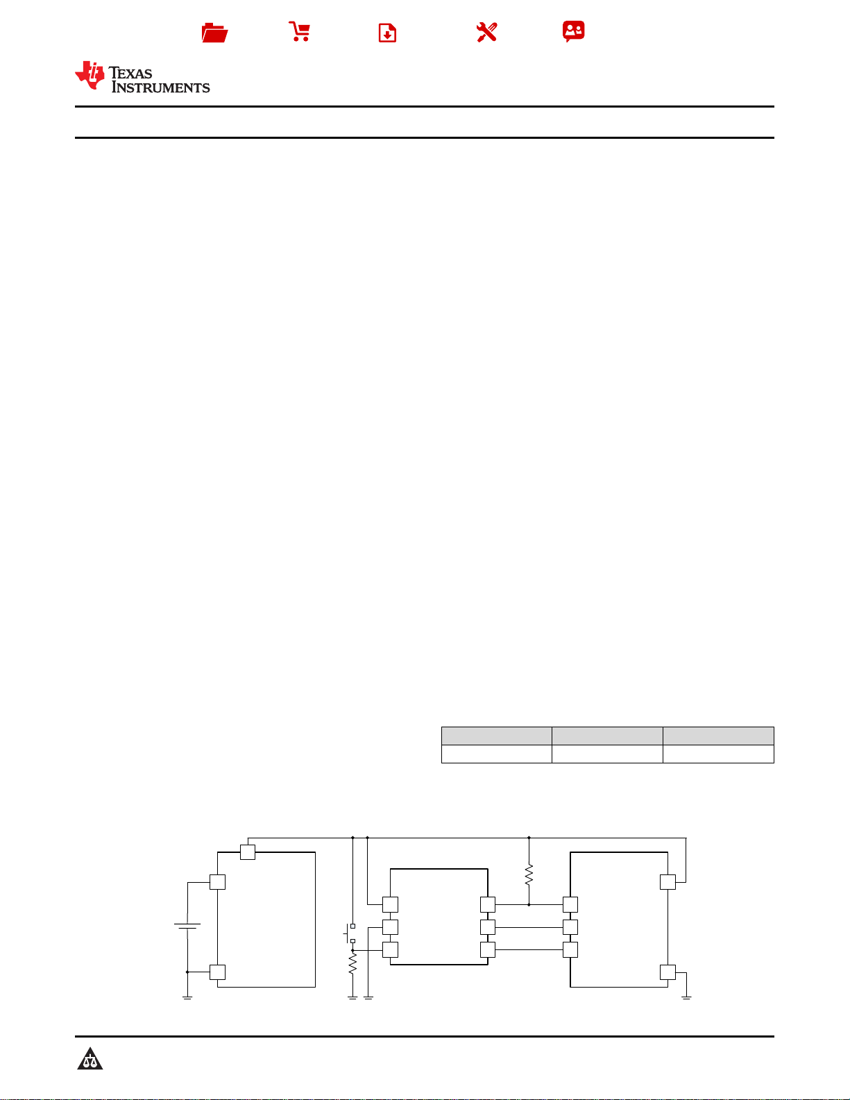
VIN
POWER MANAGEMENT
VOUT
GND
µC
GPIO
VDD
GND
Rp
GPIO
RSTn
TPL5010-Q1
VDD
GND
RSTn
WAKE
DELAY/
M_RST
DONE
R
EXT
Battery
-+
Product
Folder
Sample &
Buy
Technical
Documents
Tools &
Software
Support &
Community
TPL5010-Q1
SNAS679 –SEPTEMBER 2016
TPL5010-Q1 AEC-Q100 Nano-Power System Timer with Watchdog Function
1 Features
1
• Qualified for Automotive Applications
• AEC-Q100 Qualified with the Following Results:
– Device Temperature Grade 1: –40°C to 125°C
Ambient Operating Temperature Range
– Device HBM ESD Classification Level 2
– Device CDM ESD Classification Level C5
• Current Consumption of 35 nA (typ) at 2.5 V
• Supply Voltage from 1.8 V to 5.5 V
• Selectable Time Intervals 100 ms to 7200 s
• Timer Accuracy 1% (Typical)
• Resistor Selectable Time Interval
• Watchdog Functionality
• Manual Reset
• TPL5x10Q Family of AEC-Q100 Nano-Power
System Timers
• TPL5010-Q1 - Supply Current 35 nA
– Low Power Timer
– Watchdog Function
– Programmable Delay Range
– Manual Reset
• TPL5110-Q1 - Supply Current 35 nA
– Low Power Timer
– MOS-Driver
– Programmable Delay Range
– Manual Reset
– One-Shot Feature
2 Applications
• Electric Vehicles
• Always On Systems
• Battery powered systems
• Clutch Actuator circuit
• Car Door Handle circuit
• Smart Key
• Remote current sensor
• Intruder Detection
3 Description
The TPL5010-Q1 Nano Timer is a low power, AECQ100 qualified timer with a watchdog feature ideal for
system wake up in duty cycled or battery powered
applications. In such systems the microcontroller
timer can be used for system wake-up, but if the
timer sleep current is high, up to 60-80% of the total
system current can be consumed by the
microcontroller timer in this sleep mode. Consuming
only 35 nA, the TPL5010-Q1 can replace the
functionality of the integrated microcontroller timer
and allow the microcontroller to be placed in a much
lower power mode. Such power savings extend the
operating life of batteries and enable the use of
significantly smaller batteries making the TPL5010Q1 ideal for power sensitive applications.. The
TPL5010-Q1 provides selectable timing intervals from
100 ms to 7200 s and is designed for interrupt-driven
applications. Some standards (such as EN50271)
require implementation of a watchdog for safety and
the TPL5010-Q1 realizes this watchdog function at
almost no additional power consumption. The
TPL5010-Q1 is available in a 6-pin SOT23 package.
Device Information
PART NUMBER PACKAGE BODY SIZE (NOM)
TPL5010-Q1 SOT23 (6) 3.00 mm x 3.00 mm
(1) For all available packages, see the orderable addendum at
the end of the datasheet.
(1)
Simplified Application
1
An IMPORTANT NOTICE at the end of this data sheet addresses availability, warranty, changes, use in safety-critical applications,
intellectual property matters and other important disclaimers. PRODUCTION DATA.
Page 2
TPL5010-Q1
SNAS679 –SEPTEMBER 2016
www.ti.com
Table of Contents
1 Features.................................................................. 1
2 Applications ........................................................... 1
3 Description ............................................................. 1
4 Revision History..................................................... 2
5 Device Comparison Table..................................... 2
6 Pin Configuration and Functions......................... 3
7 Specifications......................................................... 4
7.1 Absolute Maximum Ratings ...................................... 4
7.2 ESD Ratings.............................................................. 4
7.3 Recommended Operating Conditions ...................... 4
7.4 Thermal Information ................................................. 4
7.5 Electrical Characteristics........................................... 5
7.6 Timing Requirements ............................................... 6
7.7 Typical Characteristics.............................................. 7
8 Detailed Description.............................................. 8
8.1 Overview ................................................................... 8
8.2 Functional Block Diagram......................................... 8
4 Revision History
DATE REVISION NOTES
September 2016 * Initial release.
8.3 Feature Description................................................... 8
8.4 Device Functional Modes.......................................... 9
8.5 Programming ............................................................ 9
9 Application and Implementation ........................ 15
9.1 Application Information............................................ 15
9.2 Typical Application ................................................. 15
10 Power Supply Recommendations ..................... 17
11 Layout................................................................... 17
11.1 Layout Guidelines ................................................. 17
11.2 Layout Example .................................................... 17
12 Device and Documentation Support................. 18
12.1 Receiving Notification of Documentation Updates 18
12.2 Community Resources.......................................... 18
12.3 Trademarks........................................................... 18
12.4 Electrostatic Discharge Caution............................ 18
12.5 Glossary................................................................ 18
13 Mechanical, Packaging, and Orderable
Information........................................................... 18
5 Device Comparison Table
TPL5x10Q Family of AEC-Q100 Nano- Power System Timers
PART NUMBER SUPPLY CURRENT (Typ) SPECIAL FEATURES
TPL5010-Q1 35 nA
TPL5110-Q1 35 nA
Low Power Timer
Watchdog Function
Programmable Delay Range
Manual Reset
Low Power Timer
MOS-Driver
Programmable Delay Range
Manual Reset
One-Shot Feature
2
Submit Documentation Feedback Copyright © 2016, Texas Instruments Incorporated
Product Folder Links: TPL5010-Q1
Page 3
TPL5010-Q1
VDD
GND
RSTn
WAKE
DELAY/
M_RST
DONE
1
2
3 4
5
6
TPL5010-Q1
www.ti.com
SNAS679 –SEPTEMBER 2016
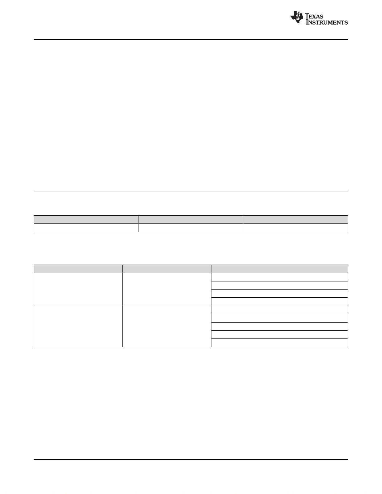
6 Pin Configuration and Functions
SOT23
6-Pin DDC
Top View
Table 1. Pin Functions
PIN
NO. NAME
1 VDD P Supply voltage
2 GND G Ground
3 DELAY/
M_RST
4 DONE I Logic Input for watchdog functionality Digital signal driven by the µC to indicate successful
5 WAKE O Timer output signal generated every t
6 RSTn O Reset Output (open drain output) Digital signal to RESET the µC, pull-up resistance is
(1) G= Ground, P= Power, O= Output, I= Input.
(1)
TYPE
I Time Interval set and Manual Reset Resistance between this pin and GND is used to
period.
DESCRIPTION APPLICATION INFORMATION
select the time interval. The reset switch is also
connected to this pin.
processing of the WAKE signal.
Digital pulsed signal to wake up the µC at the end of
IP
the programmed time interval.
required
Product Folder Links: TPL5010-Q1
Submit Documentation FeedbackCopyright © 2016, Texas Instruments Incorporated
3
Page 4
TPL5010-Q1
SNAS679 –SEPTEMBER 2016
www.ti.com
7 Specifications
7.1 Absolute Maximum Ratings
over operating free-air temperature range (unless otherwise noted)
Supply voltage (VDD-GND) –0.3 6.0 V
Input voltage at any pin
(2)
Input current on any pin –5 5 mA
T
stg
T
J
Storage temperature –65 150 °C
Junction temperature
(3)
(1) Stresses beyond those listed under Absolute Maximum Ratings may cause permanent damage to the device. These are stress ratings
only, which do not imply functional operation of the device at these or any other conditions beyond those indicated under Recommended
Operating Conditions . Exposure to absolute-maximum-rated conditions for extended periods may affect device reliability.
(2) The voltage between any two pins should not exceed 6V.
(3) The maximum power dissipation is a function of TJ(MAX), θJA, and the ambient temperature, TA. The maximum allowable power
dissipation at any ambient temperature is PDMAX = (TJ(MAX) - TA)/ θJA. All numbers apply for packages soldered directly onto a PC
board.
7.2 ESD Ratings
V
(ESD)
Electrostatic discharge
(1) AEC Q100-002 indicates that HBM stressing shall be in accordance with ANSI/ESDA/JEDEC JS-001 specification.
Human-body model, per AEC Q100-002
Charged-device model (CDM), per AEC Q10-011 ±750
(1)
MIN MAX UNIT
–0.3 VDD + 0.3 V
150 °C
VALUE UNIT
(1)
±2000
V
7.3 Recommended Operating Conditions
over operating free-air temperature range (unless otherwise noted)
MIN NOM MAX UNIT
Supply voltage (VDD-GND) 1.8 5.5 V
Temperature –40 125 °C
7.4 Thermal Information
TPL5010-Q1
THERMAL METRIC
R
θJA
R
θJC(top)
R
θJB
ψ
JT
ψ
JB
Junction-to-ambient thermal resistance 163 °C/W
Junction-to-case (top) thermal resistance 26 °C/W
Junction-to-board thermal resistance 57 °C/W
Junction-to-top characterization parameter 7.5 °C/W
Junction-to-board characterization parameter 57 °C/W
(1) For more information about traditional and new thermal metrics, see the Semiconductor and IC Package Thermal Metrics application
report.
(1)
UNITSOT23
6 PINS
4
Submit Documentation Feedback Copyright © 2016, Texas Instruments Incorporated
Product Folder Links: TPL5010-Q1
Page 5
TPL5010-Q1
www.ti.com
SNAS679 –SEPTEMBER 2016
7.5 Electrical Characteristics
TA= 25°C, VDD-GND=2.5 V (unless otherwise stated)
PARAMETER TEST CONDITIONS MIN
POWER SUPPLY
IDD Supply current
TIMER
t
IP
Time interval period
Time interval setting accuracy
Timer interval setting accuracy over
supply voltage
t
OSC
Oscillator accuracy –0.5% 0.5%
Oscillator accuracy over
temperature
Oscillator accuracy over supply
voltage
Oscillator accuracy over life time
t
DONE
t
RSTn
t
WAKE
Minimum DONE pulse width
RSTn pulse width 320 ms
WAKE pulse width 20 ms
t_Rext Time to convert Rext
DIGITAL LOGIC LEVELS
VIH Minimum logic high threshold DONE
pin
VIL Maximum logic low threshold DONE
pin
VOH Logic output high-level WAKE pin
VOL Logic output low-level WAKE pin
VOL
IOH
VIH
RSTn
RSTn
M_RST
RSTn logic output low-level IOL= –1 mA 0.3 V
RSTn high-level output current VOH
Minimum logic high threshold
DELAY/M_RST pin
(1) Values apply only for factory testing conditions at the temperature indicated. Factory testing conditions result in very limited self-heating
of the device such that TJ= TA.No specification of parametric performance is indicated in the electrical tables under conditions of
internal self-heating where TJ> TA. Absolute Maximum Ratings indicate junction temperature limits beyond which the device may be
permanently degraded, either mechanically or electrically.
(2) Limits are specified by testing, design, or statistical analysis at 25°C. Limits over the operating temperature range are specified through
correlations using statistical quality control (SQC) method.
(3) Typical values represent the most likely parametric norm as determined at the time of characterization. Actual typical values may vary
over time and will also depend on the application and configuration. The typical values are not tested and are not specified on shipped
production material.
(4) The supply current excludes load and pull-up resistor current. Input pins are at GND or VDD.
(5) This parameter is specified by design and/or characterization and is not tested in production.
(6) The accuracy for time interval settings below 1 second is ±100 ms.
(7) Operational life time test procedure equivalent to 10 years.
(4)
(5)
(6)
(5)
(5)
(7)
(5)
(5)
(5)
(1)
(2)
TYP
(3)
MAX
(2)
UNIT
Operation mode 35 50 nA
Digital conversion of external
200 400 µA
resistance (Rext)
1650 selectable time
Intervals
Min time interval 100 ms
Max time
7200
interval
s
Excluding the precision of Rext ±0.6%
1.8 V ≤ VDD ≤ 5.5 V ±25 ppm/V
-40°C ≤ TA≤ 125°C 150 ppm/°C
1.8 V ≤ VDD ≤ 5.5 V ±0.4 %/V
0.24%
100 ns
100 ms
0.7 ×
V
VDD
0.3 ×
V
VDD
Iout = 100 µA VDD – 0.3 V
Iout = 1 mA VDD – 0.7 V
Iout = –100 µA 0.3 V
Iout = –1 mA 0.7 V
= VDD 1 nA
RSTn
1.5 V
Product Folder Links: TPL5010-Q1
Submit Documentation FeedbackCopyright © 2016, Texas Instruments Incorporated
5
Page 6
WAKE
VDD
DONE
RSTn
t
t
IP
t
tt
R_EXT
+ t
RSTn
t
t
tD
DONE
t
t
DONE
tr
RSTn
tf
RSTn
tr
WAKE
tf
WAKE
tt
RSTn+tDB
t
tt
RSTn
+ tIPt
DELAY/
M_RST
tt
WAKE
t
tt
M_RST
tt
RSTn
t
TPL5010-Q1
SNAS679 –SEPTEMBER 2016
www.ti.com
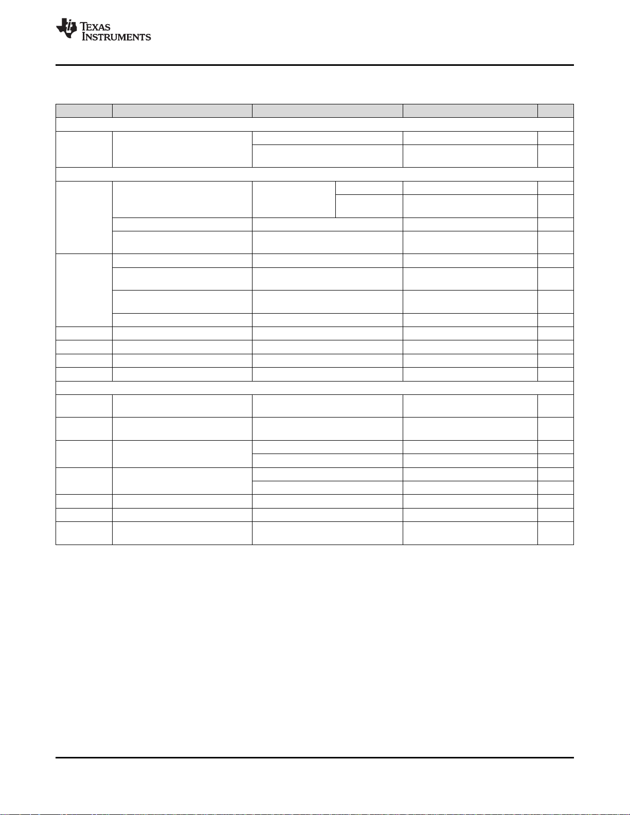
7.6 Timing Requirements
(1)
MIN
tr
RSTn
tf
RSTn
tr
WAKE
tf
WAKE
tD
DONE
t
M_RST
t
DB
Rise Time RSTn
Fall time RSTn
Rise time WAKE
Fall time WAKE
DONE to RSTn or WAKE to
DONE delay
Minimum valid manual reset
De-bounce manual reset 20 ms
(3)
(3)
(3)
(3)
Capacitive load 50 pF, Rpull-up 100 kΩ 11 µs
Capacitive load 50 pF, Rpull-up 100 kΩ 50 ns
Capacitive load 50 pF 50 ns
Capacitive load 50 pF 50 ns
Min delay
Max delay
(3)
Observation time 30 ms 20 ms
(4)
(4)
(1) Limits are specified by testing, design, or statistical analysis at 25°C. Limits over the operating temperature range are specified through
correlations using statistical quality control (SQC) method.
(2) Typical values represent the most likely parametric norm as determined at the time of characterization. Actual typical values may vary
over time and will also depend on the application and configuration. The typical values are not tested and are not specified on shipped
production material.
(3) This parameter is specified by design and/or characterization and is not tested in production.
(4) In case of RSTn from its falling edge, in case of WAKE, from its rising edge.
NOM
(2)
MAX
(1)
UNIT
100 ns
tIP–20 ms
Figure 1. TPL5010-Q1 Timing
6
Submit Documentation Feedback Copyright © 2016, Texas Instruments Incorporated
Product Folder Links: TPL5010-Q1
Page 7
Accuracy (%)
Frequency
0
5%
10%
15%
20%
25%
30%
35%
40%
-1 -0.8 -0.6 -0.4 -0.2 0 0.2 0.4 0.6 0.8
Time (s)
Supply current (PA)
0 0.1 0.2 0.3 0.4 0.5 0.6 0.7 0.8 0.9 1
0.01
0.1
1
10
100
1000
POR
R
EXT
READING
TIMER MODE
Supply Voltage (V)
Oscillator accuracy (%)
1.5 1.9 2.3 2.7 3.1 3.5 3.9 4.3 4.7 5.1 5.5
-1
-0.5
0
0.5
1
1.5
2
TA= -40°C
TA= 25°C
TA= 70°C
TA= 105°C
TA= 125°C
Temperature (°C)
Oscillator accuracy (%)
-40 -25 -10 5 20 35 50 65 80 95 110 125
-1
-0.5
0
0.5
1
1.5
2
VDD= 1.8V
VDD= 2.5V
VDD= 3.3V
VDD= 5.5V
Temperature (°C)
Supply current (nA)
-40 -25 -10 5 20 35 50 65 80 95 110 125
20
30
40
50
60
70
80
90
100
VDD= 1.8V
VDD= 2.5V
VDD= 3.3V
VDD= 5.5V
Supply Voltage (V)
Supply current (nA)
1.5 1.9 2.3 2.7 3.1 3.5 3.9 4.3 4.7 5.1 5.5
20
30
40
50
60
70
80
90
100
TA= -40°C
TA= 25°C
TA= 70°C
TA= 105°C
TA = 125°C
www.ti.com
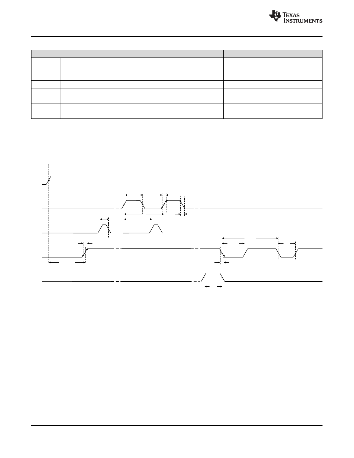
7.7 Typical Characteristics
TPL5010-Q1
SNAS679 –SEPTEMBER 2016
Figure 2. IDDvs V
DD
Figure 4. Oscillator Accuracy vs V
DD
Figure 3. IDDvs Temperature
Figure 5. Oscillator Accuracy vs Temperature
Figure 6. IDDvs Time
number of
observations >
Product Folder Links: TPL5010-Q1
1 s < tIP≤ 7200 s
20000
Figure 7. Time Interval Setting Accuracy
Submit Documentation FeedbackCopyright © 2016, Texas Instruments Incorporated
7
Page 8
WAKE
DONE
RSTn
DELAY/
M_RST
t
t
IP
t
t
t
IP
t
tt
RSTn
+ tIPt
MISSED
DONE
LOW FREQUENCY
OSCILLATOR
FREQUENCY
DIVIDER
RSTn
WAKE
VDD
GND
DELAY/
M_RST
DECODER
&
MANUAL RESET
DETECTOR
LOGIC
CONTROL
DONE
TPL5010-Q1
SNAS679 –SEPTEMBER 2016
www.ti.com
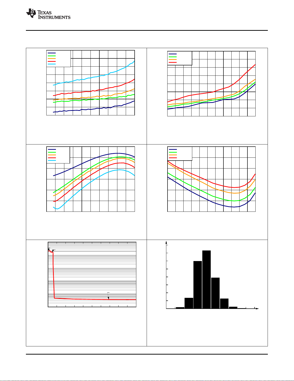
8 Detailed Description
8.1 Overview
The TPL5010-Q1 is a system wakeup timer with a watchdog feature, ideal for low power applications. TPL5010Q1 is ideal for use in interrupt-driven applications and provides selectable timing from 100 ms to 7200 s.
8.2 Functional Block Diagram
8.3 Feature Description
The DONE, WAKE and RSTn signals are used to implement the watchdog function. The TPL5010-Q1 is
programmed to issue a periodic WAKE pulse to a µC which is in sleep or standby mode. After receiving the
WAKE pulse, the µC must issue a DONE signal to the TPL5010-Q1 at least 20 ms before the rising edge of the
next WAKE pulse. If the DONE signal is not asserted, the TPL5010-Q1 asserts the RSTn signal to reset the µC.
A manual reset function is realized by momentarily pulling the DELAY/M_RST pin to VDD.
Figure 8. Watchdog
8.3.1 WAKE
The WAKE pulse is sent out from the TPL5010-Q1 when the programmed time interval starts (except at the
beginning of the first cycle or if in the previous interval the DONE has not been received).
This signal is normally low.
8.3.2 DONE
The DONE pin is driven by a µC to signal successful processing of the WAKE signal. The TPL5010-Q1
recognizes a valid DONE signal as a low to high transition; if two or more DONE signals are received within the
time interval, only the first DONE signal is processed.
The DONE signal resets the counter of the watchdog only. If the DONE signal is received when the WAKE is still
high, the WAKE will go low as soon as the DONE is recognized.
8
Submit Documentation Feedback Copyright © 2016, Texas Instruments Incorporated
Product Folder Links: TPL5010-Q1
Page 9

WAKE
DONE
RSTn
DELAY/
M_RST
POR
RESISTANCE
READING
t
t
IP
t
tt
R_EXT
+ t
RSTn
+ tIPt
TPL5010-Q1
www.ti.com
SNAS679 –SEPTEMBER 2016
Feature Description (continued)
8.3.3 RSTn
To implement the reset interface between the TPL5010-Q1 and the µC a pull-up resistance is required. 100 kΩ is
recommended, to minimize current.
During the POR and the reading of the REXT the RSTn signal is LOW.
RSTn is asserted (LOW) for either one of the following conditions:
• 1. If the DELAY/M_RST pin is high for at least two consecutive cycles of the internal oscillator (approximately
20 ms).
• 2. At the beginning of a new time interval if DONE is not received at least 20 ms before the next WAKE rising
edge (see Figure 8).
8.4 Device Functional Modes
8.4.1 Startup
During startup, after POR, the TPL5010-Q1 executes a one-time measurement of the resistance attached to the
DELAY/M_RST pin in order to determine the desired time interval for WAKE. This measurement interval is
t
. During this measurement a constant current is temporarily flowing into R
R_EXT
EXT
.
Figure 9. Startup
8.4.2 Normal Operating Mode
During normal operating mode, the TPL5010-Q1 asserts periodic WAKE pulses in response to valid DONE
pulses from the µC. If either a manual reset is applied (logic HIGH on DELAY/M_RST pin) or the µC does not
issue a DONE pulse within the required time, the TPL5010-Q1 asserts the RSTn signal to the µC and restarts its
internal counters. See Figure 8 and Figure 10 .
8.5 Programming
8.5.1 Configuring the WAKE Interval with the DELAY/M_RST Pin
The time interval between 2 adjacent WAKE pulses (rising edges) is selectable through an external resistance
(R
) between the DELAY/M_RST pin and ground. The value of the resistance R
EXT
POR. The allowable range of R
Timer Interval Selection Using External Resistance for how to set the WAKE pulse interval using R
is 500 Ω to 170 kΩ. At least a 1% precision resistance is recommended. See
EXT
The time between 2 adjacent RESET signals (falling edges) or between a RESET (falling edge) and a WAKE
(rising edge) is given by the sum of the programmed time interval and the t
Product Folder Links: TPL5010-Q1
(reset pulse width).
RSTn
is converted one time after
EXT
Submit Documentation FeedbackCopyright © 2016, Texas Instruments Incorporated
EXT
.
9
Page 10

WAKE
DONE
RSTn
DELAY/
M_RST
tt
M_RST
t ttDBt
tt
RSTn
+ tIPt
t
t
IP
t
tt
M_RST
t
NOT VALID M_RST VALID M_RST
ANY RESET
TPL5010-Q1
SNAS679 –SEPTEMBER 2016
www.ti.com
Programming (continued)
8.5.2 Manual Reset
If VDD is connected to the DELAY/M_RST pin, the TPL5010-Q1 recognizes this as a manual reset condition. In
this case the time interval is not set. If the manual reset is asserted during the POR or during the reading
procedure, the reading procedure is aborted and is re-started as soon as the manual reset switch is released. A
pulse on the DELAY/M_RST pin is recognized as a valid manual reset only if it lasts at least 20 ms (observation
time is 30 ms).
A valid manual reset resets all the counters inside the TPL5010-Q1. The counters restart only when the high
digital voltage at DELAY/M_RST is removed and the next t
RSTn
is elapsed.
Figure 10. Manual Reset
8.5.2.1 DELAY/M_RST
A resistance in the range between 500 Ω and 170 kΩ needs to be connected in order to select a valid time
interval. At the POR and during the reading of the resistance the DELAY/M_RST is connected to an analog
signal chain though a mux. After the reading of the resistance the analog circuit is switched off and the
DELAY/RST is connected to a digital circuit.
The manual reset detection is supported with a de-bounce feature which makes the TPL5010-Q1 insensitive to
the glitches on the DELAY/M_RST pin. When a valid manual reset signal is asserted on the DELAY/M_RST pin,
the RSTn signal is asserted LOW after a delay of t
tDB+ t
. Due to the asynchronous nature of the manual reset signal and its arbitrary duration, the LOW status
RSTn
. It remains LOW after a valid manual reset is asserted +
M_RST
of the RSTn signal maybe affected by an uncertainty of about ±5 ms.
A valid manual reset puts all the digital output signals at their default values:
• WAKE = LOW
• RSTn = asserted LOW
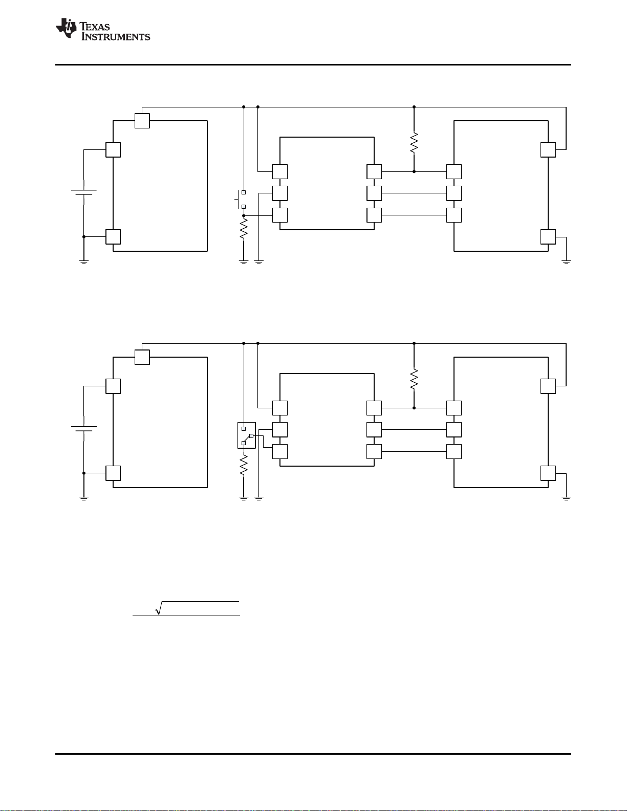
8.5.2.2 Circuitry
The manual reset may be implemented using a switch (momentary mechanical action). The TPL5010-Q1 offers 2
possible approaches according to the power consumption constraints of the application.
10
Submit Documentation Feedback Copyright © 2016, Texas Instruments Incorporated
Product Folder Links: TPL5010-Q1
Page 11
¸
¸
¹
·
¨
¨
©
§
a
Tcabb
R
EXT
2
1004
100
2
VIN
POWER MANAGEMENT
VOUT
GND
µC
GPIO
VDD
GND
Rp
GPIO
RSTn
TPL5010-Q1
VDD
GND
RSTn
WAKE
DELAY/
M_RST
DONE
R
EXT
Battery
-+
VIN
POWER MANAGEMENT
VOUT
GND
µC
GPIO
VDD
GND
Rp
GPIO
RSTn
TPL5010-Q1
VDD
GND
RSTn
WAKE
DELAY/
M_RST
DONE
R
EXT
Battery
-+
TPL5010-Q1
www.ti.com
SNAS679 –SEPTEMBER 2016
Programming (continued)
Figure 11. Manual Reset with SPST Switch
For use cases that do not require the lowest power consumption, using a single pole single throw switch may
offer a lower cost solution. The DELAY/M_RST pin may be directly connected to VDD with R
The current drawn from the supply voltage during the reset is given by VDD/R
EXT
.
in the circuit.
EXT
Figure 12. Manual Reset with SPDT Switch
The reset function may also be asserted by switching DELAY/M_RST from R
to VDD using a single pole
EXT
double throw switch, which will provide a lower power solution for the manual reset, because no current flows.
8.5.3 Timer Interval Selection Using External Resistance
In order to set the time interval, the external resistance R
is selected according the following formula:
EXT
where
• T is the desired time interval in seconds
• R
• a, b, c are coefficients depending on the range of the time interval (1)
is the resistance value to use in Ω
EXT
Product Folder Links: TPL5010-Q1
Submit Documentation FeedbackCopyright © 2016, Texas Instruments Incorporated
11
Page 12

¸
¸
¹
·
¨
¨
©
§
1284.0*2
8*1008889.25611284.0*49861.469861.46
100
2
EXT
R
TPL5010-Q1
SNAS679 –SEPTEMBER 2016
Programming (continued)
Table 2. Coefficients for Equation 1
SET
1 1 < T ≤ 5 0.2253 –20.7654 570.5679
2 5 < T ≤ 10 –0.1284 46.9861 –2651.8889
3 10 < T ≤ 100 0.1972 –19.3450 692.1201
4 100 < T ≤ 1000 0.2617 –56.2407 5957.7934
5 T > 1000 0.3177 –136.2571 34522.4680
EXAMPLE
Required time interval: 8 s
The coefficient set to be selected is the number 2. The formula becomes:
The resistance value is 10.18 kΩ.
Table 3 and Table 4 contain example values of tIPand their corresponding value of R
TIME
INTERVAL
RANGE (s)
a b c
EXT
www.ti.com
(2)
.
Table 3. First 9 Time Intervals
tIP(ms) RESISTANCE (Ω) CLOSEST REAL VALUE (Ω)
100 500 500 1.0 // 1.0
200 1000 1000 300 1500 1500 2.43 // 3.92
400 2000 2000 500 2500 2500 4.42 // 5.76
600 3000 3000 5.36 // 6.81
700 3500 3500 4.75 // 13.5
800 4000 4000 6.19 // 11.3
900 4500 4501 6.19 // 16.5
PARALLEL OF TWO 1% TOLERANCE
RESISTORS (kΩ)
Table 4. Most Common Time Intervals Between 1 s to 2 h
t
IP
1 s 5.20 5.202 7.15 // 19.1
2 s 6.79 6.788 12.4 // 15.0
3 s 7.64 7.628 12.7// 19.1
4 s 8.30 8.306 14.7 // 19.1
5 s 8.85 8.852 16.5 // 19.1
6 s 9.27 9.223 18.2 // 18.7
7 s 9.71 9.673 19.1 // 19.6
8 s 10.18 10.180 11.5 // 8.87
9 s 10.68 10.68 17.8 // 26.7
10 s 11.20 11.199 15.0 // 44.2
20 s 14.41 14.405 16.9 // 97.6
30 s 16.78 16.778 32.4 // 34.8
40 s 18.75 18.748 22.6 // 110.0
CALCULATED RESISTANCE (kΩ)
CLOSEST REAL
VALUE (kΩ)
PARALLEL OF TWO 1% TOLERANCE
RESISTORS (kΩ)
12
Submit Documentation Feedback Copyright © 2016, Texas Instruments Incorporated
Product Folder Links: TPL5010-Q1
Page 13

»
¼
º
«
¬
ª
100
EXT
D
R
INTR
»
¼
º
«
¬
ª
¸
¸
¹
·
¨
¨
©
§
c
R
b
R
aINTT
DD
ADC
100100100
1
2
2
DESIRED
ADCDESIRED
T
TT
Err 100
www.ti.com
Table 4. Most Common Time Intervals Between 1 s to 2 h (continued)
t
IP
50 s 20.047 20.047 28.7 // 66.5
1 min 22.02 22.021 40.2 // 48.7
2 min 29.35 29.349 35.7 // 165.0
3 min 34.73 34.729 63.4 // 76.8
4 min 39.11 39.097 63.4 // 102.0
5 min 42.90 42.887 54.9 // 196.0
6 min 46.29 46.301 75.0 // 121.0
7 min 49.38 49.392 97.6 // 100.0
8 min 52.24 52.224 88.7 // 127.0
9 min 54.92 54.902 86.6 // 150.0
10 min 57.44 57.437 107.0 // 124.0
20 min 77.57 77.579 140.0 // 174.0
30 min 92.43 92.233 182.0 // 187.0
40 min 104.67 104.625 130.0 // 536.00
50 min 115.33 115.331 150.0 // 499.00
1 h 124.91 124.856 221.0 // 287.00
1 h 30 min 149.39 149.398 165.0 // 1580.0
2 h 170.00 170.00 340.0 // 340.0
CALCULATED RESISTANCE (kΩ)
CLOSEST REAL
VALUE (kΩ)
PARALLEL OF TWO 1% TOLERANCE
RESISTORS (kΩ)
TPL5010-Q1
SNAS679 –SEPTEMBER 2016
8.5.4 Quantization Error
The TPL5010-Q1 can generate 1650 discrete timer intervals in the range of 100 ms to 7200 s. The first 9
intervals are multiples of 100 ms. The remaining 1641 intervals cover the range between 1 s to 7200 s. Because
they are discrete intervals, there is a quantization error associated with each value.
The quantization error can be evaluated according to the following formula:
Where:
where
• R
• a, b, c are the coefficients of the equation listed in Table 2 (5)
is the resistance calculated with Equation 1
EXT
8.5.5 Error Due to Real External Resistance
R
is a theoretical value and may not be available in standard commercial resistor values. It is possible to
EXT
closely approach the theoretical R
using two or more standard values in parallel. However, standard values
EXT
are characterized by a certain tolerance. This tolerance will affect the accuracy of the time interval.
The accuracy can be evaluated using the following procedure:
1. Evaluate the min and max values of R
EXT(REXT_MIN
, R
EXT_MAX
with Equation 1 using the selected commercial
resistance values and their tolerances.
2. Evaluate the time intervals (T
ADC_MIN[REXT_MIN
3. Find the errors using Equation 3 with T
ADC_MIN
], T
ADC_MAX[REXT_MAX
, T
ADC_MAX
.
]) with Equation 4.
The results of the formula indicate the accuracy of the time interval.
Submit Documentation FeedbackCopyright © 2016, Texas Instruments Incorporated
Product Folder Links: TPL5010-Q1
(3)
(4)
13
Page 14

3
Tolerance
Rnu
n
R
2
2
2
1
////
21
¸
¹
·
¨
©
§
¸
¹
·
¨
©
§
R
u
R
u
RuR
RR
TPL5010-Q1
SNAS679 –SEPTEMBER 2016
The example below illustrates the procedure.
• Desired time interval , T_desired = 600 s
• Required R
From Table 4, R
, from Equation 1, R
EXT
can be built with a parallel combination of two commercial values with 1% tolerance: R1=107
EXT
= 57.44 kΩ
EXT
kΩ, R2=124 kΩ. The uncertainty of the equivalent parallel resistance can be found using Equation 6.
Where uRn (n=1,2) represent the uncertainty of a resistance,
The uncertainty of the parallel resistance is 0.82%, meaning the value of R
56.96 kΩ and R
EXT_MAX
Using these value of R
586.85 s and T
ADC_MAX
= 57.90 kΩ.
, the digitized timer intervals calculated with Equation 4 are respectively T
EXT
= 611.3 s, giving an error range of –1.88% / +2.19%. The asymmetry of the error range is
may range between R
EXT
due to the quadratic transfer function of the resistance digitizer.
www.ti.com
EXT_MIN
ADC_MIN
(6)
(7)
=
=
14
Submit Documentation Feedback Copyright © 2016, Texas Instruments Incorporated
Product Folder Links: TPL5010-Q1
Page 15
Temp 29°C
CO 0PPM
TIME xx:xx
Date xx/xx/xxxx
DISPLAY
Button
ButtonButton
Button
KEYBOARD
GAS
SENSOR
VIN
POWER MANAGEMENT
VOUT
GND
Rp
100k
RST
µC
GPIO
GPIO
VDD
GND
SCL
LMP91000
SDA
VOUT
VREF
GND
SDA
SCL
ADC
CE
RE
WE
MENB
CE
RE
WE
VDD
VOLTAGE
REFERENCE
GND
VOUTVIN
Rp
100k
Rp
100k
Lithium
ion battery
-
+
GPIO
GPIO
GPIO
GPIO
TPL5010-Q1
VDD
GND
RSTn
WAKE
DELAY/
M_RST
DONE
R
EXT
TPL5010-Q1
www.ti.com
SNAS679 –SEPTEMBER 2016
9 Application and Implementation
NOTE
Information in the following applications sections is not part of the TI component
specification, and TI does not warrant its accuracy or completeness. TI’s customers are
responsible for determining suitability of components for their purposes. Customers should
validate and test their design implementation to confirm system functionality.
9.1 Application Information
In battery-powered applications, one design constraint is the need for low current consumption. The TPL5010-Q1
is ideal for applications where there is a need to monitor environmental conditions at a fixed time interval. Often
in these applications, a watchdog or other internal timer in a µC is used to implement a wakeup function. Using
the TPL5010-Q1 to implement the watchdog function will consume only tens of nA, significantly improving the
power consumption of the system.
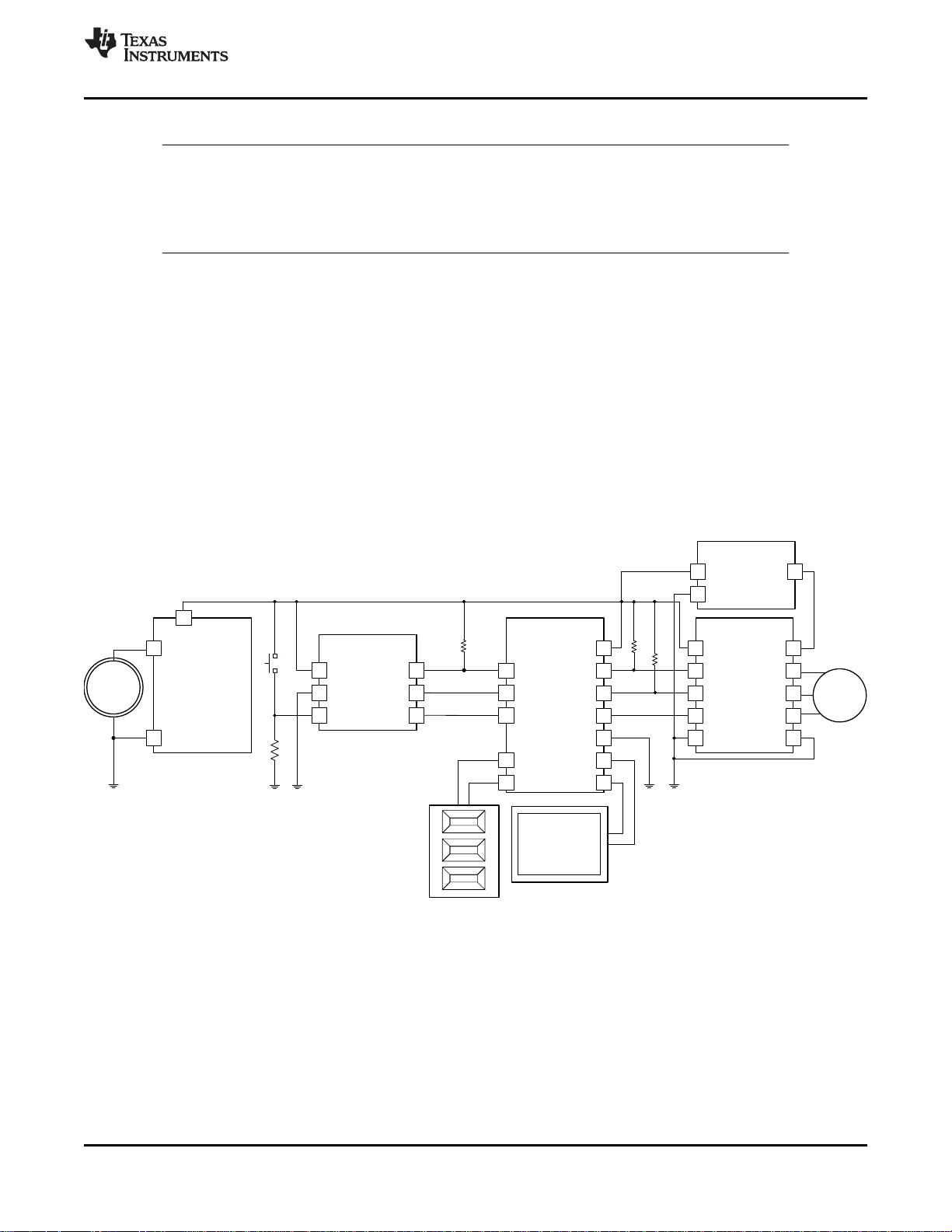
9.2 Typical Application
The TPL5010-Q1 can be used in conjunction with environment sensors to build a low-power environment datalogger, such as an air quality data-logger. In this application, due to the monitored phenomena, the µC and the
front end of the sensor spend most of the time in the idle state, waiting for the next logging interval, usually a few
hundred of milliseconds. Figure 13 illustrates a data logging application based on a µC, and a front end for a gas
sensor based on the LMP91000.
Figure 13. Data-Logger
9.2.1 Design Requirements
The design is driven by the low current consumption constraint. The data are usually acquired on a rate that
ranges between 1 s and 10 s. The highest necessity is the maximization of the battery life. The TPL5010-Q1
helps achieve that goal because it allows putting the µC in its lowest power mode. The TPL5010-Q1 will take
care of the watchdog and the timing.
Product Folder Links: TPL5010-Q1
Submit Documentation FeedbackCopyright © 2016, Texas Instruments Incorporated
15
Page 16

Time
Current consumption
Without TPL5010-Q1
With TPL5010-Q1
TPL5010-Q1
SNAS679 –SEPTEMBER 2016
www.ti.com
Typical Application (continued)
9.2.2 Detailed Design Procedure
When the main constraint is the battery life, the selection of a low-power voltage reference, µC, and display is
mandatory. The first step in the design is the calculation of the power consumption of the devices in their
different mode of operations. For instance, the LMP91000 burns most of the power when in gas measurement
mode, then according to the connected gas sensor it has 2 idle states: stand-by and deep sleep. The same is
true for the µC, such as one of the MSP430 family, which can be placed in one of its lower power modes, such
as LMP3.5 or LMP4.5. In this case, the TPL5010-Q1 can be used to implement the watchdog and wakeup timing
functions.
After the power budget calculation it is possible to select the appropriate time interval which satisfies the
application constraints and maximize the life of the battery.
9.2.3 Application Curves
16
Submit Documentation Feedback Copyright © 2016, Texas Instruments Incorporated
Figure 14. Effect of TPL5010-Q1 on Current Consumption
Product Folder Links: TPL5010-Q1
Page 17

TPL5010-Q1
www.ti.com
SNAS679 –SEPTEMBER 2016
10 Power Supply Recommendations
The TPL5010-Q1 requires a voltage supply within 1.8 V and 5.5 V. A multilayer ceramic bypass X7R capacitor of
0.1 μF between VDD and GND pin is recommended.
11 Layout
11.1 Layout Guidelines
The DELAY/M_RST pin is sensitive to parasitic capacitance. It is suggested that the traces connecting the
resistance on this pin to GROUND be kept as short as possible to minimize parasitic capacitance. This
capacitance can affect the initial set up of the time interval. Signal integrity on the WAKE and RSTn pins is also
improved by keeping the trace length between the TPL5010-Q1 and the µC short to reduce the parasitic
capacitance.
11.2 Layout Example
Figure 15. Layout
Product Folder Links: TPL5010-Q1
Submit Documentation FeedbackCopyright © 2016, Texas Instruments Incorporated
17
Page 18

TPL5010-Q1
SNAS679 –SEPTEMBER 2016
www.ti.com
12 Device and Documentation Support
12.1 Receiving Notification of Documentation Updates
To receive notification of documentation updates, navigate to the device product folder on ti.com. In the upper
right corner, click on Alert me to register and receive a weekly digest of any product information that has
changed. For change details, review the revision history included in any revised document.
12.2 Community Resources
The following links connect to TI community resources. Linked contents are provided "AS IS" by the respective
contributors. They do not constitute TI specifications and do not necessarily reflect TI's views; see TI's Terms of
Use.
TI E2E™ Online Community TI's Engineer-to-Engineer (E2E) Community. Created to foster collaboration
among engineers. At e2e.ti.com, you can ask questions, share knowledge, explore ideas and help
solve problems with fellow engineers.
Design Support TI's Design Support Quickly find helpful E2E forums along with design support tools and
contact information for technical support.
12.3 Trademarks
E2E is a trademark of Texas Instruments.
All other trademarks are the property of their respective owners.
12.4 Electrostatic Discharge Caution
These devices have limited built-in ESD protection. The leads should be shorted together or the device placed in conductive foam
during storage or handling to prevent electrostatic damage to the MOS gates.
12.5 Glossary
SLYZ022 — TI Glossary.
This glossary lists and explains terms, acronyms, and definitions.
13 Mechanical, Packaging, and Orderable Information
The following pages include mechanical, packaging, and orderable information. This information is the most
current data available for the designated devices. This data is subject to change without notice and revision of
this document. For browser-based versions of this data sheet, refer to the left-hand navigation.
18
Submit Documentation Feedback Copyright © 2016, Texas Instruments Incorporated
Product Folder Links: TPL5010-Q1
Page 19

PACKAGE OPTION ADDENDUM
www.ti.com
PACKAGING INFORMATION
Orderable Device Status
TPL5010QDDCRQ1 ACTIVE SOT-23-THIN DDC 6 3000 RoHS & Green SN Level-1-260C-UNLIM -40 to 125 13VX
TPL5010QDDCTQ1 ACTIVE SOT-23-THIN DDC 6 250 RoHS & Green SN Level-1-260C-UNLIM -40 to 125 13VX
(1)
The marketing status values are defined as follows:
ACTIVE: Product device recommended for new designs.
LIFEBUY: TI has announced that the device will be discontinued, and a lifetime-buy period is in effect.
NRND: Not recommended for new designs. Device is in production to support existing customers, but TI does not recommend using this part in a new design.
PREVIEW: Device has been announced but is not in production. Samples may or may not be available.
OBSOLETE: TI has discontinued the production of the device.
Package Type Package
(1)
Drawing
Pins Package
Qty
Eco Plan
(2)
Lead finish/
Ball material
(6)
MSL Peak Temp
(3)
Op Temp (°C) Device Marking
(4/5)
(2)
RoHS: TI defines "RoHS" to mean semiconductor products that are compliant with the current EU RoHS requirements for all 10 RoHS substances, including the requirement that RoHS substance
do not exceed 0.1% by weight in homogeneous materials. Where designed to be soldered at high temperatures, "RoHS" products are suitable for use in specified lead-free processes. TI may
reference these types of products as "Pb-Free".
RoHS Exempt: TI defines "RoHS Exempt" to mean products that contain lead but are compliant with EU RoHS pursuant to a specific EU RoHS exemption.
Green: TI defines "Green" to mean the content of Chlorine (Cl) and Bromine (Br) based flame retardants meet JS709B low halogen requirements of <=1000ppm threshold. Antimony trioxide based
flame retardants must also meet the <=1000ppm threshold requirement.
(3)
MSL, Peak Temp. - The Moisture Sensitivity Level rating according to the JEDEC industry standard classifications, and peak solder temperature.
(4)
There may be additional marking, which relates to the logo, the lot trace code information, or the environmental category on the device.
(5)
Multiple Device Markings will be inside parentheses. Only one Device Marking contained in parentheses and separated by a "~" will appear on a device. If a line is indented then it is a continuation
of the previous line and the two combined represent the entire Device Marking for that device.
(6)
Lead finish/Ball material - Orderable Devices may have multiple material finish options. Finish options are separated by a vertical ruled line. Lead finish/Ball material values may wrap to two
lines if the finish value exceeds the maximum column width.
Important Information and Disclaimer:The information provided on this page represents TI's knowledge and belief as of the date that it is provided. TI bases its knowledge and belief on information
provided by third parties, and makes no representation or warranty as to the accuracy of such information. Efforts are underway to better integrate information from third parties. TI has taken and
continues to take reasonable steps to provide representative and accurate information but may not have conducted destructive testing or chemical analysis on incoming materials and chemicals.
TI and TI suppliers consider certain information to be proprietary, and thus CAS numbers and other limited information may not be available for release.
In no event shall TI's liability arising out of such information exceed the total purchase price of the TI part(s) at issue in this document sold by TI to Customer on an annual basis.
9-Mar-2021
Samples
Addendum-Page 1
Page 20

PACKAGE OPTION ADDENDUM
www.ti.com
OTHER QUALIFIED VERSIONS OF TPL5010-Q1 :
Catalog: TPL5010
•
NOTE: Qualified Version Definitions:
Catalog - TI's standard catalog product
•
9-Mar-2021
Addendum-Page 2
Page 21

PACKAGE OUTLINE
PIN 1
INDEX AREA
4X 0.95
1.9
SCALE 4.000
3.05
2.55
1.75
1.45
1
3
B
A
6
3.05
2.75
4
0.5
6X
0.3
0.2 C A B
SOT - 1.1 max heightDDC0006A
SOT
1.100
0.847
0.1 C
0.1
TYP
0.0
0 -8 TYP
0.20
0.12
TYP
0.6
0.3
SEATING PLANE
TYP
C
0.25
GAGE PLANE
4214841/B 11/2020
NOTES:
1. All linear dimensions are in millimeters. Any dimensions in parenthesis are for reference only. Dimensioning and tolerancing
per ASME Y14.5M.
2. This drawing is subject to change without notice.
3. Reference JEDEC MO-193.
www.ti.com
Page 22

EXAMPLE BOARD LAYOUT
SOT - 1.1 max heightDDC0006A
SOT
SOLDER MASK
OPENING
6X (0.6)
4X (0.95)
(R0.05) TYP
1
3
METAL
6X (1.1)
SYMM
(2.7)
LAND PATTERN EXAMPLE
EXPLOSED METAL SHOWN
SCALE:15X
METAL UNDER
SOLDER MASK
6
SYMM
4
SOLDER MASK
OPENING
EXPOSED METAL
EXPOSED METAL
0.07 MAX
ARROUND
NON SOLDER MASK
DEFINED
0.07 MIN
ARROUND
SOLDER MASK
DEFINED
SOLDERMASK DETAILS
NOTES: (continued)
4. Publication IPC-7351 may have alternate designs.
5. Solder mask tolerances between and around signal pads can vary based on board fabrication site.
4214841/B 11/2020
www.ti.com
Page 23

1
EXAMPLE STENCIL DESIGN
SOT - 1.1 max heightDDC0006A
SOT
SYMM
6X (1.1)
6X (0.6)
4X(0.95)
(R0.05) TYP
3
(2.7)
SOLDER PASTE EXAMPLE
BASED ON 0.125 THICK STENCIL
SCALE:15X
6
SYMM
4
4214841/B 11/2020
NOTES: (continued)
6. Laser cutting apertures with trapezoidal walls and rounded corners may offer better paste release. IPC-7525 may have alternate
design recommendations.
7. Board assembly site may have different recommendations for stencil design.
www.ti.com
Page 24

IMPORTANT NOTICE AND DISCLAIMER
TI PROVIDES TECHNICAL AND RELIABILITY DATA (INCLUDING DATASHEETS), DESIGN RESOURCES (INCLUDING REFERENCE
DESIGNS), APPLICATION OR OTHER DESIGN ADVICE, WEB TOOLS, SAFETY INFORMATION, AND OTHER RESOURCES “AS IS”
AND WITH ALL FAULTS, AND DISCLAIMS ALL WARRANTIES, EXPRESS AND IMPLIED, INCLUDING WITHOUT LIMITATION ANY
IMPLIED WARRANTIES OF MERCHANTABILITY, FITNESS FOR A PARTICULAR PURPOSE OR NON-INFRINGEMENT OF THIRD
PARTY INTELLECTUAL PROPERTY RIGHTS.
These resources are intended for skilled developers designing with TI products. You are solely responsible for (1) selecting the appropriate
TI products for your application, (2) designing, validating and testing your application, and (3) ensuring your application meets applicable
standards, and any other safety, security, or other requirements. These resources are subject to change without notice. TI grants you
permission to use these resources only for development of an application that uses the TI products described in the resource. Other
reproduction and display of these resources is prohibited. No license is granted to any other TI intellectual property right or to any third party
intellectual property right. TI disclaims responsibility for, and you will fully indemnify TI and its representatives against, any claims, damages,
costs, losses, and liabilities arising out of your use of these resources.
TI’s products are provided subject to TI’s Terms of Sale (https:www.ti.com/legal/termsofsale.html) or other applicable terms available either
on ti.com or provided in conjunction with such TI products. TI’s provision of these resources does not expand or otherwise alter TI’s
applicable warranties or warranty disclaimers for TI products.IMPORTANT NOTICE
Mailing Address: Texas Instruments, Post Office Box 655303, Dallas, Texas 75265
Copyright © 2021, Texas Instruments Incorporated
 Loading...