

TPIC6C596
POWER LOGIC 8-BIT SHIFT REGISTER
SLIS093 – MARCH 2000
D
Low r
DS(on)
D
Avalanche Energy ...30 mJ
D
Eight Power DMOS Transistor Outputs of
...7 Ω Typ
100-mA Continuous Current
D
250-mA Current Limit Capability
D
ESD Protection . . . 2500 V
D
Output Clamp Voltage . . . 33 V
D
Enhanced Cascading for Multiple Stages
D
All Registers Cleared With Single Input
D
Low Power Consumption
description
The TPIC6C596 is a monolithic, medium-voltage,
low-current power 8-bit shift register designed for
use in systems that require relatively moderate
load power such as LEDs. The device contains a
built-in voltage clamp on the outputs for inductive
transient protection. Power driver applications
include relays, solenoids, and other low-current or
medium-voltage loads.
This device contains an 8-bit serial-in, parallel-out
shift register that feeds an 8-bit D-type storage
register. Data transfers through both the shift and
storage registers on the rising edge of the shift
register clock (SRCK) and the register clock
(RCK), respectively. The storage register transfers data to the output buffer when shift register
clear (CLR
in the device are cleared. When output enable (G)
is held high, all data in the output buffers is held
) is high. When CLR is low, all registers
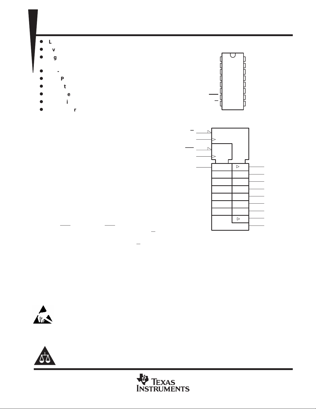
logic symbol
8
G
10
RCK
7
CLR
SRCK
SER IN
†
This symbol is in accordance with ANSI/IEEE Std 91-1984
and IEC Publication 617-12.
15
2
D OR N PACKAGE
V
CC
SER IN
DRAIN0
DRAIN1
DRAIN2
DRAIN3
CLR
G
†
EN3
C2
SRG8
R
C1
1D
(TOP VIEW)
1
16
2
15
3
14
4
13
5
12
6
11
7
10
8
9
GND
SRCK
DRAIN7
DRAIN6
DRAIN5
DRAIN4
RCK
SER OUT
2
2
3
4
5
6
11
12
13
14
9
low and all drain outputs are off. When G is held
low, data from the storage register is transparent to the output buf fers. When data in the output buf fers is low,
the DMOS transistor outputs are off. When data is high, the DMOS transistor outputs have sink-current
capability. The serial output (SER OUT) is clocked out of the device on the falling edge of SRCK to provide
additional hold time for cascaded applications. This will provide improved performance for applications where
clock signals may be skewed, devices are not located near one another, or the system must tolerate
electromagnetic interference.
DRAIN0
DRAIN1
DRAIN2
DRAIN3
DRAIN4
DRAIN5
DRAIN6
DRAIN7
SER OUT
This device contains circuits to protect its inputs and outputs against damage due to high static voltages or electrostatic fields. These
circuits have been qualified to protect this device against electrostatic discharges (ESD) of up to 2 kV according to MIL-STD-883C,
Method 3015; however, it is advised that precautions be taken to avoid application of any voltage higher than maximum-rated
voltages to these high-impedance circuits. During storage or handling, the device leads should be shorted together or the device
should be placed in conductive foam. In a circuit, unused inputs should always be connected to an appropriated logic voltage level,
preferably either VCC or ground. Specific guidelines for handling devices of this type are contained in the publication
Handling Electrostatic-Discharge-Sensitive (ESDS) Devices and Assemblies
Please be aware that an important notice concerning availability, standard warranty, and use in critical applications of
Texas Instruments semiconductor products and disclaimers thereto appears at the end of this data sheet.
PRODUCTION DATA information is current as of publication date.
Products conform to specifications per the terms of Texas Instruments
standard warranty. Production processing does not necessarily include
testing of all parameters.
POST OFFICE BOX 655303 • DALLAS, TEXAS 75265
available from Texas Instruments.
Guidelines for
Copyright 2000, Texas Instruments Incorporated
1
TPIC6C596
POWER LOGIC 8-BIT SHIFT REGISTER
SLIS093 – MARCH 2000
description (continued)
Outputs are low-side, open-drain DMOS transistors with output ratings of 33 V and 100 mA continuous
sink-current capability . Each output provides a 250-mA maximum current limit at TC = 25°C. The current limit
decreases as the junction temperature increases for additional device protection. The device also provides up
to 2500 V of ESD protection when tested using the human-body model and 200 V machine model.
The TPIC6C596 is characterized for operation over the operating case temperature range of –40°C to 125°C.
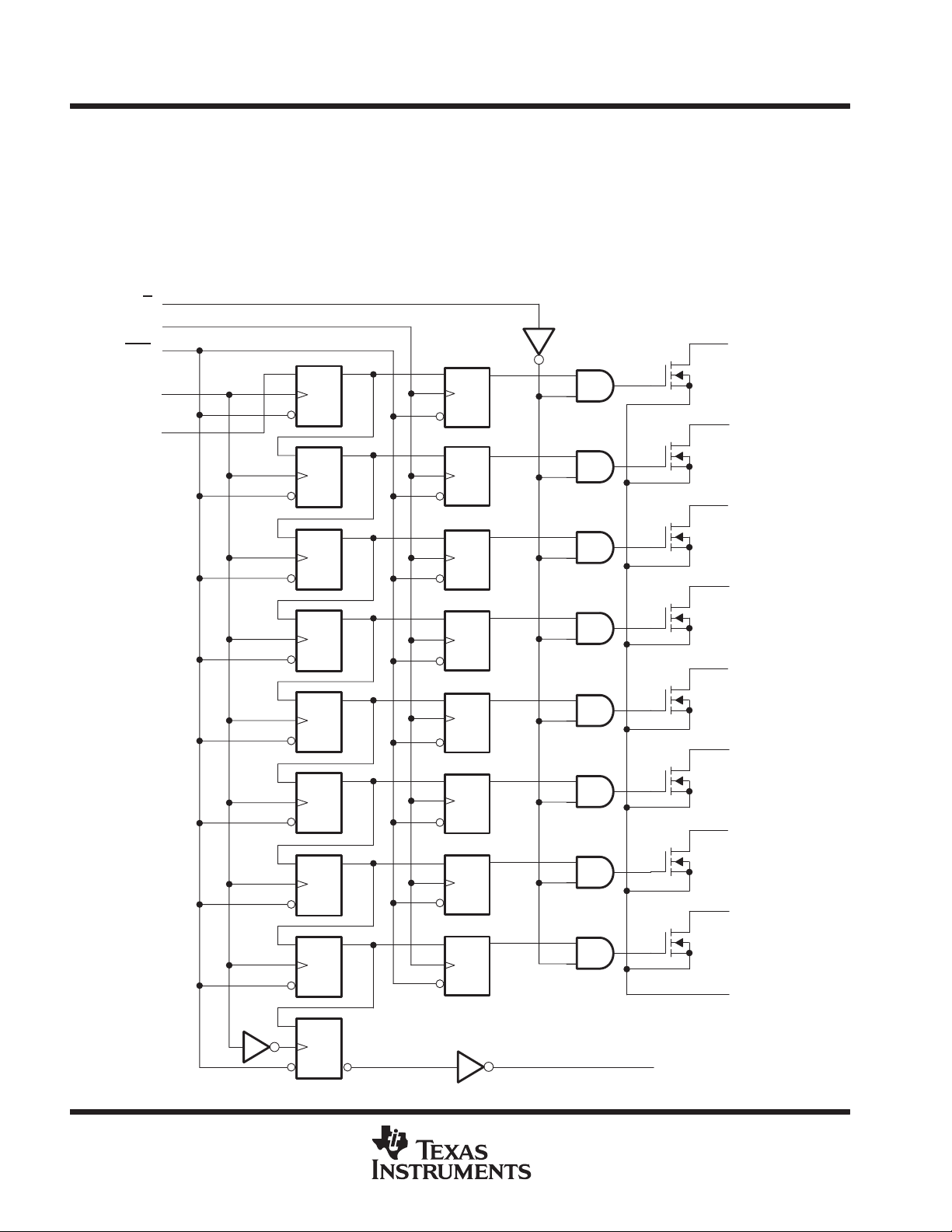
logic diagram (positive logic)
8
G
10
RCK
CLR
SRCK
SER IN
15
7
D
C1
2
CLR
D
C1
CLR
D
C2
CLR
D
C2
CLR
3
4
5
DRAIN0
DRAIN1
DRAIN2
D
C1
CLR
D
C1
CLR
D
C1
CLR
D
C1
CLR
D
C1
CLR
D
C1
CLR
D
C2
CLR
D
C2
CLR
D
C2
CLR
D
C2
CLR
D
C2
CLR
D
C2
CLR
16
6
11
12
13
14
DRAIN3
DRAIN4
DRAIN5
DRAIN6
DRAIN7
GND
D
C1
CLR
2
POST OFFICE BOX 655303 • DALLAS, TEXAS 75265
9
SER OUT
schematic of inputs and outputs
EQUIVALENT OF EACH INPUT TYPICAL OF ALL DRAIN OUTPUTS
V
CC
Input
25 V
12 V
TPIC6C596
POWER LOGIC 8-BIT SHIFT REGISTER
SLIS093 – MARCH 2000
DRAIN
33 V
20 V
GND
GND
absolute maximum ratings over recommended operating case temperature range (unless
otherwise noted)
Logic supply voltage, VCC (see Note 1) 7 V. . . . . . . . . . . . . . . . . . . . . . . . . . . . . . . . . . . . . . . . . . . . . . . . . . . . . . .
Logic input voltage range, VI –0.3 V to 7 V. . . . . . . . . . . . . . . . . . . . . . . . . . . . . . . . . . . . . . . . . . . . . . . . . . . . . . . .
Power DMOS drain-to-source voltage, VDS (see Note 2) 33 V. . . . . . . . . . . . . . . . . . . . . . . . . . . . . . . . . . . . . . . .
Continuous source-to-drain diode anode current 250 mA. . . . . . . . . . . . . . . . . . . . . . . . . . . . . . . . . . . . . . . . . . . .
Pulsed source-to-drain diode anode current (see Note 3) 500 mA. . . . . . . . . . . . . . . . . . . . . . . . . . . . . . . . . . . . .
Pulsed drain current, each output, all outputs on, I
Continuous drain current, each output, all outputs on, ID, TC = 25°C 100 mA. . . . . . . . . . . . . . . . . . . . . . . . . . .
Peak drain current single output, IDM,T
Single-pulse avalanche energy, EAS (see Figure 4) 30 mJ. . . . . . . . . . . . . . . . . . . . . . . . . . . . . . . . . . . . . . . . . . .
Avalanche current, I
Continuous total dissipation See Dissipation Rating Table. . . . . . . . . . . . . . . . . . . . . . . . . . . . . . . . . . . . . . . . . . .
Operating virtual junction temperature range, TJ –40°C to 150°C. . . . . . . . . . . . . . . . . . . . . . . . . . . . . . . . . . . . .
Operating case temperature range, TC –40°C to 125°C. . . . . . . . . . . . . . . . . . . . . . . . . . . . . . . . . . . . . . . . . . . . .
Storage temperature range, T
Lead temperature 1,6 mm (1/16 inch) from case for 10 seconds 260°C. . . . . . . . . . . . . . . . . . . . . . . . . . . . . . .
†
Stresses beyond those listed under “absolute maximum ratings” may cause permanent damage to the device. These are stress ratings only, and
functional operation of the device at these or any other conditions beyond those indicated under “recommended operating conditions” is not
implied. Exposure to absolute-maximum-rated conditions for extended periods may affect device reliability.
NOTES: 1. All voltage values are with respect to GND.
2. Each power DMOS source is internally connected to GND.
3. Pulse duration ≤ 100 µs and duty cycle ≤ 2%.
4. DRAIN supply voltage = 15 V, starting junction temperature (TJS) = 25°C, L = 1.5 H, IAS = 200 mA (see Figure 4).
†
, T
= 25°C (see Note 3) 250 mA. . . . . . . . . . . . . . . . . . .
D
C
= 25°C (see Note 3) 250 mA. . . . . . . . . . . . . . . . . . . . . . . . . . . . . . . . .
C
(see Note 4) 200 mA. . . . . . . . . . . . . . . . . . . . . . . . . . . . . . . . . . . . . . . . . . . . . . . . . . . . . .
AS
–65°C to 150°C. . . . . . . . . . . . . . . . . . . . . . . . . . . . . . . . . . . . . . . . . . . . . . . . . . .
stg
DISSIPATION RATING TABLE
PACKAGE
D 1087 mW 8.7 mW/°C 217 mW
N 1470 mW 11.7 mW/°C 294 mW
TC ≤ 25°C
POWER RATING
POST OFFICE BOX 655303 • DALLAS, TEXAS 75265
DERATING FACTOR
ABOVE TC = 25°C
POWER RATING
TC = 125°C
3
TPIC6C596
VOHHigh-level output voltage, SER OUT
V
VOLLow-level output voltage, SER OUT
V
ICCLogic supply current
V
V
A
POWER LOGIC 8-BIT SHIFT REGISTER
SLIS093 – MARCH 2000
recommended operating conditions
MIN MAX UNIT
Logic supply voltage, V
High-level input voltage, V
Low-level input voltage, V
Pulsed drain output current, TC = 25°C, VCC = 5 V, all outputs on (see Notes 3 and 5 and Figure 11) 250 mA
Setup time, SER IN high before SRCK↑, tsu (see Figure 2) 15 ns
Hold time, SER IN high after SRCK↑, th (see Figure 2) 15 ns
Pulse duration, tw (see Figure 2) 40 ns
Operating case temperature, T
NOTES: 3. Pulse duration ≤ 100 µs and duty cycle ≤ 2%.
5. Technique should limit TJ – TC to 10°C maximum.
CC
IH
IL
C
electrical characteristics, VCC = 5 V, TC = 25°C (unless otherwise noted)
PARAMETER TEST CONDITIONS MIN TYP MAX UNIT
V
(BR)DSX
V
SD
I
IH
I
IL
I
CC(FRQ)
I
N
I
DSX
r
DS(on)
NOTES: 5. Technique should limit TJ – TC to 10°C maximum.
Drain-to-source breakdown voltage ID = 1 mA 33 37 V
Source-to-drain diode forward voltage IF = 100 mA 0.85 1.2 V
p
p
High-level input current VCC = 5.5 V, VI = V
Low-level input current VCC = 5.5 V, VI = 0 –1 µA
pp
Logic supply current at frequency
Nominal current
Off-state drain current
Static drain-source on-state resistance
6. These parameters are measured with voltage-sensing contacts separate from the current-carrying contacts.
7. Nominal current is defined for a consistent comparison between devices from different sources. It is the current that produces a
voltage drop of 0.5 V at TC = 85°C.
IOH = –20 µA, VCC = 4.5 V 4.4 4.49
IOH = –4 mA, VCC = 4.5 V 4 4.2
IOL = 20 µA, VCC = 4.5 V 0.005 0.1
IOL = 4 mA, VCC = 4.5 V 0.3 0.5
CC
= 5.5
CC
f
= 5 MHz,
SRCK
All outputs off,
V
TC = 85°C,
VDS = 30 V, VCC = 5.5 V 0.1 5
VDS = 30 V,
TC = 125°C
ID = 50 mA,
VCC = 4.5 V
ID = 50 mA,
TC = 125°C,
VCC = 4.5 V
ID = 100 mA,
VCC = 4.5 V
DS(on)
= 0.5 V,
All outputs off 20 200
All outputs on 150 500
CL = 30 pF,
See Figures 2 and 6
IN = ID,
See Notes 5, 6 and 7
VCC = 5.5 V,
See Notes 5 and 6
and Figures 7 and 8
4.5 5.5 V
0.85 V
CC
0.15 V
CC
–40 125 °C
1 µA
1.2 5 mA
90 mA
0.15 8
6.5 9
9.9 12
6.8 10
V
V
µ
µA
Ω
4
POST OFFICE BOX 655303 • DALLAS, TEXAS 75265

L
,
D
,
F
, µ ,
ns
R
Thermal resistance, junction-to-ambient
All 8 outputs with equal power
°C/W
switching characteristics, VCC = 5 V, TC = 25°C
PARAMETER TEST CONDITIONS MIN TYP MAX UNIT
t
PLH
t
PHL
t
r
t
f
t
pd
f
(SRCK)
t
a
t
rr
NOTES: 5. Technique should limit TJ – TC to 10°C maximum.
thermal resistance
θJA
Propagation delay time, low-to-high-level output from G 80 ns
Propagation delay time, high-to-low-level output from G
Rise time, drain output
Fall time, drain output 80 ns
Propagation delay time, SRCK↓ to SEROUT
Serial clock frequency
Reverse-recovery-current rise time
Reverse-recovery time
6. These parameters are measured with voltage-sensing contacts separate from the current-carrying contacts.
8. This is the maximum serial clock frequency assuming cascaded operation where serial data is passed from one stage to a second
stage. The clock period allows for SRCK → SEROUT propagation delay and setup time plus some timing margin.
PARAMETER TEST CONDITIONS MIN MAX UNIT
D package
N package
POWER LOGIC 8-BIT SHIFT REGISTER
C
= 30 pF, I
See Figures 1, 2, and 9
CL = 30 pF, ID = 75 mA,
See Figure 2
CL = 30 pF, ID = 75 mA,
See Note 8
I
= 100 mA, di/dt = 10 A/µs,
See Notes 5 and 6 and Figure 3
= 75 mA,
p
TPIC6C596
SLIS093 – MARCH 2000
50 ns
100 ns
15 ns
10 MHz
100
120
p
115
85
°
PARAMETER MEASUREMENT INFORMATION
I
D
3–6,
11–14
15 V
RL = 200 Ω
Output
CL = 30 pF
(see Note B)
SRCK
SER IN
RCK
CLR
DRAIN1
76543210
G
VOLTAGE WAVEFORMS
5 V
0 V
5 V
0 V
5 V
0 V
5 V
0 V
5 V
0 V
15 V
0.5 V
5 V
1
7
15
Word
Generator
(see Note A)
NOTES: A. The word generator has the following characteristics: tr ≤ 10 ns, tf ≤ 10 ns, tw = 300 ns, pulsed repetition rate (PRR) = 5 kHz,
ZO = 50 Ω.
B. CL includes probe and jig capacitance.
2
10
8
V
CLR
SRCK
SER IN
RCK
G
TEST CIRCUIT
CC
DUT
GND
16
DRAIN
Figure 1. Resistive-Load Test Circuit and Voltage Waveforms
POST OFFICE BOX 655303 • DALLAS, TEXAS 75265
5

TPIC6C596
POWER LOGIC 8-BIT SHIFT REGISTER
SLIS093 – MARCH 2000
PARAMETER MEASUREMENT INFORMATION
Word
Generator
(see Note A)
7
CLR
15
SRCK
2
SER IN
10
RCK
8
G
TEST CIRCUIT
5 V 15 V
1
V
CC
DUT
DRAIN
GND
16
I
D
3–6,
11–14
RL = 200 Ω
Output
CL = 30 pF
(see Note B)
Output
SRCK
SER IN
SRCK
G
50%
t
PLH
90%
10%
t
r
SWITCHING TIMES
50%
t
su
50%
t
w
INPUT SETUP AND HOLD WAVEFORMS
50%50%
t
pd
50%
t
90%
h
50%
t
t
pd
PHL
10%
t
5 V
0 V
24 V
0.5 V
f
5 V
0 V
5 V
0 V
SER OUT
NOTES: A. The word generator has the following characteristics: tr ≤ 10 ns, tf ≤ 10 ns, tw = 300 ns, pulsed repetition rate (PRR) = 5 kHz,
ZO = 50 Ω.
B. CL includes probe and jig capacitance.
50% 50%
SER OUT PROPAGATION DELAY WAVEFORM
Figure 2. Test Circuit, Switching Times, and Voltage Waveforms
6
POST OFFICE BOX 655303 • DALLAS, TEXAS 75265

TPIC6C596
POWER LOGIC 8-BIT SHIFT REGISTER
SLIS093 – MARCH 2000
PARAMETER MEASUREMENT INFORMATION
DRAIN
Circuit
Under
Test
I
(see Note A)
t
1
V
(see Note B)
NOTES: A. The DRAIN terminal under test is connected to the TP K test point. All other terminals are connected together and connected to the
TP A test point.
B. The VGG amplitude and RG are adjusted for di/dt = 10 A/µs. A VGG double-pulse train is used to set IF = 0.1 A, where t1 = 10 µs,
t2 = 7 µs, and t3 = 3 µs.
F
t
2
t
3
R
G
GG
50 Ω
TEST CIRCUIT CURRENT WAVEFORM
TP K
L = 0.85 mH
Driver
TP A
2500 µF
250 V
15 V
0.1 A
+
–
I
RM
I
F
0
di/dt = 10 A/µs
t
a
t
rr
25% of I
RM
Figure 3. Reverse-Recovery-Current Test Circuit and Waveforms of Source-to-Drain Diode
I
D
3–6,
11–14
15 V
30 Ω
1.5 H
(BR)DSX
V
DS
× tav/2 = 30 mJ.
Input
V
See Note B
I
D
DS
VOLTAGE AND CURRENT WAVEFORMS
5 V
1
7
CLR
15
SRCK
Word
Generator
(see Note A)
SINGLE-PULSE AVALANCHE ENERGY TEST CIRCUIT
NOTES: A. The word generator has the following characteristics: tr ≤ 10 ns, tf ≤ 10 ns, ZO = 50 Ω.
B. Input pulse duration, tw, is increased until peak current IAS = 200 mA.
Energy test level is defined as EAS = IAS × V
2
10
8
SER IN
RCK
G
V
CC
DUT
GND
DRAIN
16
Figure 4. Single-Pulse Avalanche Energy Test Circuit and Waveforms
t
w
t
av
5 V
0 V
IAS = 200 mA
V
(BR)DSX
MIN
= 33 V
POST OFFICE BOX 655303 • DALLAS, TEXAS 75265
7

TPIC6C596
POWER LOGIC 8-BIT SHIFT REGISTER
SLIS093 – MARCH 2000
TYPICAL CHARACTERISTICS
PEAK AVALANCHE CURRENT
vs
TIME DURATION OF AVALANCHE
1
TC = 25°C
0.4
0.2
0.1
0.04
AS
I – Peak Avalanche Current – A
0.02
0.01
0.1 0.2 10.4 2 104
tav – Time Duration of Avalanche – ms
Figure 5
DRAIN-TO-SOURCE ON-STATE RESISTANCE
vs
DRAIN CURRENT
30
Ω
VCC = 5 V
See Note A
25
TC = 125°C
20
SUPPLY CURRENT
vs
FREQUENCY
6
VCC = 5 V
TC = –40°C to 125°C
5
4
3
2
CC
I – Supply Current – mA
1
0
0.1 1 10 100
f – Frequency – MHz
Figure 6
STATIC DRAIN-TO-SOURCE ON-STATE RESISTANCE
vs
Ω
12
10
8
LOGIC SUPPLY VOLTAGE
ID = 50 mA
TC = 125°C
See Note A
8
15
10
5
– Drain-to-Source On-State Resistance –r
DS(on)
0
50 70 90 110 130
ID – Drain Current – mA
Figure 7
TC = 25°C
TC = –40°C
150 170 190
POST OFFICE BOX 655303 • DALLAS, TEXAS 75265
250
– Static Drain-to-Source On-State Resistance –r
DS(on)
TC = 25°C
6
4
2
0
4 4.5 5 5.5
TC = – 40°C
VCC – Logic Supply Voltage – V
Figure 8
6 6.5 7

TPIC6C596
POWER LOGIC 8-BIT SHIFT REGISTER
SLIS093 – MARCH 2000
TYPICAL CHARACTERISTICS
SWITCHING TIME
vs
CASE TEMPERATURE
140
ID = 75 mA
See Note A
120
100
t
r
t
r
80
60
Switching Time – ns
40
20
0
–50 –25 0 25
NOTE A: Technique should limit TJ – TC to 10°C maximum.
t
PLH
t
PHL
50 100 125
75
TC – Case Temperature – °C
Figure 9
POST OFFICE BOX 655303 • DALLAS, TEXAS 75265
9

TPIC6C596
POWER LOGIC 8-BIT SHIFT REGISTER
SLIS093 – MARCH 2000
THERMAL INFORMATION
MAXIMUM CONTINUOUS
DRAIN CURRENT OF EACH OUTPUT
vs
NUMBER OF OUTPUTS CONDUCTING
SIMULTANEOUSLY
0.25
0.2
0.15
of Each Output – A
0.05
– Maximum Continuous Drain Current
D
I
0
12 3 4
N – Number of Outputs Conducting Simultaneously
TC = 125°C
TC = 25°C
TC = 100°C0.1
Figure 10
VCC = 5 V
5867
MAXIMUM PEAK DRAIN CURRENT
OF EACH OUTPUT
vs
NUMBER OF OUTPUTS CONDUCTING
SIMULTANEOUSLY
0.3
0.25
0.2
0.15
d = 80%
0.1
VCC = 5 V
TC = 25°C
0.05
d = tw/t
period
– Maximum Peak Drain Current of Each Output – A
D
I
= 1 ms/t
0
12 34 5
N – Number of Outputs Conducting Simultaneously
period
d = 20%
d = 50%
Figure 11
d = 10%
678
10
POST OFFICE BOX 655303 • DALLAS, TEXAS 75265

†
TPIC6C596
POWER LOGIC 8-BIT SHIFT REGISTER
SLIS093 – MARCH 2000
THERMAL INFORMATION
D PACKAGE
NORMALIZED JUNCTION-TO-AMBIENT THERMAL RESISTANCE
vs
PULSE DURATION
10
C/W
°
DC Conditions
1
d = 0.5
d = 0.2
d = 0.1
0.1
d = 0.05
d = 0.02
d = 0.01
0.01
Single Pulse
– Normalized Junction-to-Ambient Thermal Resistance –
0.001
JAθ
R
0.0001
0.0001 0.001 0.01 0.1 1 10
tw – Pulse Duration – s
†
Device mounted on FR4 printed-circuit board with no heat sink
NOTES: ZθA(t) = r(t) R
tw = pulse duration
tc = cycle time
d = duty cycle = tw/t
θJA
c
t
w
t
c
Figure 12
I
D
0
POST OFFICE BOX 655303 • DALLAS, TEXAS 75265
11

IMPORTANT NOTICE
T exas Instruments and its subsidiaries (TI) reserve the right to make changes to their products or to discontinue
any product or service without notice, and advise customers to obtain the latest version of relevant information
to verify, before placing orders, that information being relied on is current and complete. All products are sold
subject to the terms and conditions of sale supplied at the time of order acknowledgment, including those
pertaining to warranty, patent infringement, and limitation of liability.
TI warrants performance of its semiconductor products to the specifications applicable at the time of sale in
accordance with TI’s standard warranty. Testing and other quality control techniques are utilized to the extent
TI deems necessary to support this warranty . Specific testing of all parameters of each device is not necessarily
performed, except those mandated by government requirements.
Customers are responsible for their applications using TI components.
In order to minimize risks associated with the customer’s applications, adequate design and operating
safeguards must be provided by the customer to minimize inherent or procedural hazards.
TI assumes no liability for applications assistance or customer product design. TI does not warrant or represent
that any license, either express or implied, is granted under any patent right, copyright, mask work right, or other
intellectual property right of TI covering or relating to any combination, machine, or process in which such
semiconductor products or services might be or are used. TI’s publication of information regarding any third
party’s products or services does not constitute TI’s approval, warranty or endorsement thereof.
Copyright 2000, Texas Instruments Incorporated
 Loading...