

Page 1
User's Guide
SLVUAN6–June 2016
TPD1E0B04 Evaluation Module
This user's guide describes the characteristics, operation, and use of the TPD1E0B04 EVM evaluation
module (EVM). This EVM includes six TPD1E0B04s in various configurations for testing. Five
TPD1E0B04s are configured for IEC 61000-4-2 compliance testing and one is configured for 2-port sparameter analysis. This user's guide includes setup instructions, schematic diagrams, a bill of materials,
and printed-circuit board layout drawings for the evaluation module.
Contents
1 Introduction ................................................................................................................... 2
2 Definitions..................................................................................................................... 2
3 Setup .......................................................................................................................... 3
3.1 IEC 61000-4-2 ESD Rating Tests ................................................................................ 3
3.2 Scattering Parameters ............................................................................................. 4
3.3 ±8-kV ESD Clamping Waveforms ................................................................................ 4
4 Board Layout ................................................................................................................. 6
5 Schematics ................................................................................................................... 6
6 Bill of Materials............................................................................................................... 7
List of Figures
1 Ideal Contact Discharge Waveform of the Output Current of the ESD Simulator at 4-kV ......................... 3
2 System Level ESD Test Setup............................................................................................. 4
3 TPD1E0B04EVM Top Layer and Silkscreen............................................................................. 6
4 TPD1E0B04EVM Schematic ............................................................................................... 6
List of Tables
1 IEC 61000-4-2 Test Levels ................................................................................................ 2
2 Waveform Parameters in Contact Discharge Mode..................................................................... 2
3 Bill of Materials............................................................................................................... 7
SLVUAN6–June 2016
Submit Documentation Feedback
Copyright © 2016, Texas Instruments Incorporated
TPD1E0B04 Evaluation Module
1
Page 2
Introduction
1 Introduction
Texas Instrument’s TPD1E0B04 evaluation module helps designers evaluate the operation and
performance of the TPD1E0B04 device. The TPD1E0B04 is a unidirectional TVS ESD protection diode for
HDMI 2.0 and USB 3.1 Gen II Super-speed data line protection. The TPD1E0B04 is rated to dissipate
ESD strikes at the maximum level specified in the IEC 61000-4-2 international standard (Level 4).
The EVM contains six TPD1E0B04s. Five TPD1E0B04s (D1 – D5) are configured with test points for
striking ESD to the protection pins. One TPD1E0B04 (D6) is configured with 2 SMA (J1 and J2)
connectors for 2-port analysis with a vector network analyzer. TPD1E0B04 (D6) can also be used for
capturing clamping waveforms with an oscilloscope during an ESD test. Caution must be taken when
capturing clamping waveforms during an ESD event so as not to damage the oscilloscope. A proper
procedure is outlined in Section 3.3.1.
2 Definitions
Contact Discharge — a method of testing in which the electrode of the ESD simulator is held in contact
with the device-under-test (DUT).
Air Discharge — a method of testing in which the charged electrode of the ESD simulator approaches
the DUT, and a spark to the DUT actuates the discharge.
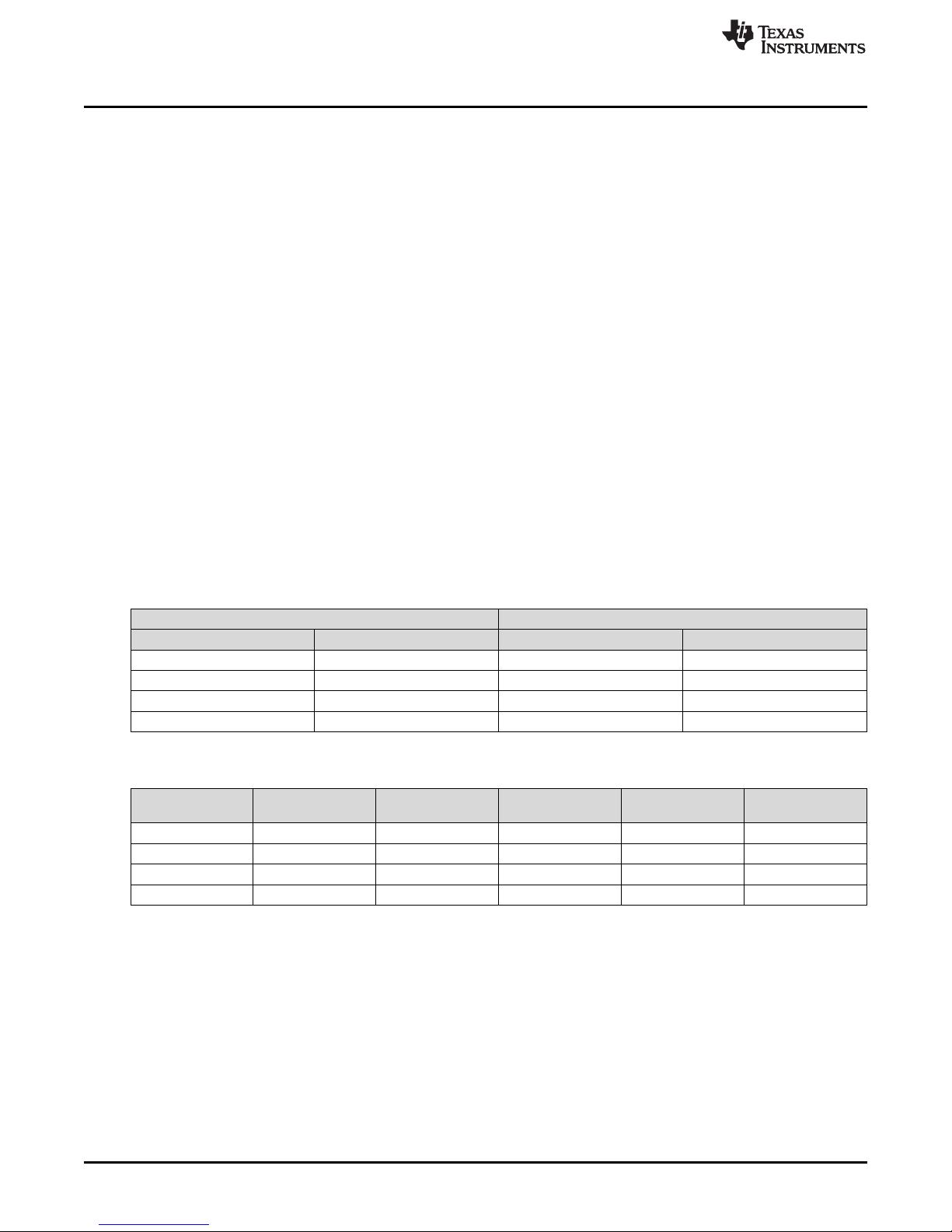
ESD Simulator — a device that outputs IEC 61000-4-2 compliance ESD waveforms shown in Figure 1
with adjustable ranges shown in Table 1 and Table 2.
IEC 61000-4-2 has 4 classes of protection levels. Classes 1 – 4 are shown in Table 1. Stress tests
must be incrementally tested to level 4 as shown in Table 2 until the point of failure. If the DUT
does not fail at 8-kV, testing can continue in 2-kV increments until failure.
www.ti.com
Contact Discharge Air Discharge
Class Test Voltage [± kV] Class Test Voltage [± kV]
1 2 1 2
2 4 2 4
3 6 3 8
4 8 4 15
Table 2. Waveform Parameters in Contact Discharge Mode
Stress Level Step Simulator Voltage
[kV]
1 2 7.5 0.8 4 2
2 4 15 0.8 8 4
3 6 22.5 0.8 12 6
4 8 30 0.8 16 8
Table 1. IEC 61000-4-2 Test Levels
Ipeak ±15%
[A]
Rise Time ±25%
[ns]
Current at 30 ns
±30% [A]
Current at 60 ns
±30% [A]
2
TPD1E0B04 Evaluation Module
Copyright © 2016, Texas Instruments Incorporated
Submit Documentation Feedback
SLVUAN6–June 2016
Page 3
0
10
20
30
0 20 40 60 80 100
Current (A)
Time (ns)
I
PEAK
90% I
PEAK
10% I
PEAK
800 ps 90/10 rise time
www.ti.com
Figure 1. Ideal Contact Discharge Waveform of the Output Current of the ESD Simulator at 4-kV
3 Setup
This section describes the intended use of the EVM. A generalized outline of the procedure given in IEC
61000-4-2 is described here. IEC 61000-4-2 must be referred to for a more specific testing outline. Basic
configurations for collecting s-parameters and ESD clamping waveforms are outlined as well.
3.1 IEC 61000-4-2 ESD Rating Tests
TPD1E0B04 (D1 – D5) can be used for destructive electrostatic discharge (ESD) pass or fail strikes.
Specifically, they can be used for both IEC 61000-4-2 air and contact discharge tests. The procedure in
Section 3.1.1 ensures proper testing setup and method for both discharge tests. Each IO has a Test Pad
(TP1 – TP5) directly connected to it for striking ESD.
Setup
3.1.1 Test Method and Set-Up
An example test setup is shown in Figure 2. Details of the testing table and ground planes can be found in
the IEC 61000-4-2 test procedure. Ground the EVM using the banana connector J3. Discharge the ESD
simulator on any of the test points TP1 – TP5. Contact and air-gap discharge are tested using the same
simulator with the same discharge waveform. While the simulator is in direct contact with the test point
during contact, it is not during air-gap.
SLVUAN6–June 2016
Submit Documentation Feedback
Copyright © 2016, Texas Instruments Incorporated
TPD1E0B04 Evaluation Module
3
Page 4

ESD Simulator
Typical Position for
Direct Discharge
Ground Reference Plane
Power and Ground Connection
DUT or System
Horizontal Coupling
Plane (HCP)
To Wall
Ground
470 kO
470 kO
Non-conducting Table
Insulation
Setup
www.ti.com
3.1.2 Evaluation of Test Results
3.2 Scattering Parameters
3.3 ±8-kV ESD Clamping Waveforms
Figure 2. System Level ESD Test Setup
Connect the tested device on the EVM to a curve tracer both before and after ESD testing. After each
incremental level, if the IV-curve of the ESD protection diode shifts ±0.1 V, or leakage current increases by
a factor of ten, then the device is permanently damaged by ESD.
A TPD1E0B04 (D6) is configured with 2 SMA (J1 and J2) connectors to allow 2-port analysis with a vector
network analyzer. Connect Port 1 to J1 and Port 2 to J2. This configuration allows for the following
terminology in 2-port analysis:
• S11: Return loss
• S21: Insertion loss
A TPD1E0B04 (D6) has two SMA connectors (J1 and J2) which can be used for capturing clamping
waveforms with an oscilloscope during an ESD strike. Caution must be taken when capturing clamping
waveforms during an ESD event so as not to damage the oscilloscope. The procedures in Section 3.3.1
outlines a proper method.
4
TPD1E0B04 Evaluation Module
Copyright © 2016, Texas Instruments Incorporated
SLVUAN6–June 2016
Submit Documentation Feedback
Page 5

www.ti.com
3.3.1 Oscilloscope Setup
Without a proper procedure, capturing ESD clamping waveforms exposes the oscilloscope to potential
voltages higher than the rating of the equipment. Proper methodology can mitigate any risk in this
operation.
Recommended Measurement Equipment:
• One 2-GHz bandwidth (minimum of 1 GHz) oscilloscope.
• Two 10X 50-Ω attenuators
• One 50-Ω shielded SMA cable.
Procedure
In order to protect the oscilloscope, attenuation of the measured signal is required. Here is a procedure for
testing D3:
1. Ground the EVM using the banana connector J3.
2. Attach two 10X attenuators in series to the oscilloscope channel being used.
3. Attach the 50-Ω shielded SMA cable between J2 and the attenuators.
4. Set the scope attenuation factor to 100X.
5. Set the oscilloscope to trigger on a positive edge for (+) ESD and a negative edge for (–) ESD strikes.
The trigger voltage magnitude must be set to 20 V.
6. Following Section 3.1.1, strike contact ESD to J1.Pin1.
Recommended settings for the time axis is 20 ns/div and for the voltage axis is 10 V division.
The voltage levels of the ESD applied to J1.Pin1 must not exceed ±8 kV while capturing clamping
waveforms.
Setup
SLVUAN6–June 2016
Submit Documentation Feedback
Copyright © 2016, Texas Instruments Incorporated
TPD1E0B04 Evaluation Module
5
Page 6

Board Layout
4 Board Layout
This section provides the TPD1E0B04EVM board layout. TPD1E0B04EVM is a 4-layer board of FR408HR
at 0.062 inch thickness. Layers 2, 3, and 4 are ground planes and not shown here.
www.ti.com
5 Schematics
Figure 3. TPD1E0B04EVM Top Layer and Silkscreen
Figure 4. TPD1E0B04EVM Schematic
6
TPD1E0B04 Evaluation Module
Copyright © 2016, Texas Instruments Incorporated
Submit Documentation Feedback
SLVUAN6–June 2016
Page 7

www.ti.com
6 Bill of Materials
Bill of Materials
Table 3. Bill of Materials
Count RefDes Description Package
6 D1, D2, D3, D4,
D5, D6
2 J1, J2 Connector, TH, End launch
1 J3 Standard Banana Jack,
1-Channel ESD Protection
Device for Super-Speed (up
to 6 Gbps) Interface,
DPL0002A
SMA 50 Ω
Insulated, Black
Reference
DPL0002A TPD1E0B04DPL Texas Instruments
Connector, TH,
End launch SMA
6092 6092 Keystone
Part Number MFR
142-0761-881 Johnson
SLVUAN6–June 2016
Submit Documentation Feedback
Copyright © 2016, Texas Instruments Incorporated
TPD1E0B04 Evaluation Module
7
Page 8

IMPORTANT NOTICE
Texas Instruments Incorporated and its subsidiaries (TI) reserve the right to make corrections, enhancements, improvements and other
changes to its semiconductor products and services per JESD46, latest issue, and to discontinue any product or service per JESD48, latest
issue. Buyers should obtain the latest relevant information before placing orders and should verify that such information is current and
complete. All semiconductor products (also referred to herein as “components”) are sold subject to TI’s terms and conditions of sale
supplied at the time of order acknowledgment.
TI warrants performance of its components to the specifications applicable at the time of sale, in accordance with the warranty in TI’s terms
and conditions of sale of semiconductor products. Testing and other quality control techniques are used to the extent TI deems necessary
to support this warranty. Except where mandated by applicable law, testing of all parameters of each component is not necessarily
performed.
TI assumes no liability for applications assistance or the design of Buyers’ products. Buyers are responsible for their products and
applications using TI components. To minimize the risks associated with Buyers’ products and applications, Buyers should provide
adequate design and operating safeguards.
TI does not warrant or represent that any license, either express or implied, is granted under any patent right, copyright, mask work right, or
other intellectual property right relating to any combination, machine, or process in which TI components or services are used. Information
published by TI regarding third-party products or services does not constitute a license to use such products or services or a warranty or
endorsement thereof. Use of such information may require a license from a third party under the patents or other intellectual property of the
third party, or a license from TI under the patents or other intellectual property of TI.
Reproduction of significant portions of TI information in TI data books or data sheets is permissible only if reproduction is without alteration
and is accompanied by all associated warranties, conditions, limitations, and notices. TI is not responsible or liable for such altered
documentation. Information of third parties may be subject to additional restrictions.
Resale of TI components or services with statements different from or beyond the parameters stated by TI for that component or service
voids all express and any implied warranties for the associated TI component or service and is an unfair and deceptive business practice.
TI is not responsible or liable for any such statements.
Buyer acknowledges and agrees that it is solely responsible for compliance with all legal, regulatory and safety-related requirements
concerning its products, and any use of TI components in its applications, notwithstanding any applications-related information or support
that may be provided by TI. Buyer represents and agrees that it has all the necessary expertise to create and implement safeguards which
anticipate dangerous consequences of failures, monitor failures and their consequences, lessen the likelihood of failures that might cause
harm and take appropriate remedial actions. Buyer will fully indemnify TI and its representatives against any damages arising out of the use
of any TI components in safety-critical applications.
In some cases, TI components may be promoted specifically to facilitate safety-related applications. With such components, TI’s goal is to
help enable customers to design and create their own end-product solutions that meet applicable functional safety standards and
requirements. Nonetheless, such components are subject to these terms.
No TI components are authorized for use in FDA Class III (or similar life-critical medical equipment) unless authorized officers of the parties
have executed a special agreement specifically governing such use.
Only those TI components which TI has specifically designated as military grade or “enhanced plastic” are designed and intended for use in
military/aerospace applications or environments. Buyer acknowledges and agrees that any military or aerospace use of TI components
which have not been so designated is solely at the Buyer's risk, and that Buyer is solely responsible for compliance with all legal and
regulatory requirements in connection with such use.
TI has specifically designated certain components as meeting ISO/TS16949 requirements, mainly for automotive use. In any case of use of
non-designated products, TI will not be responsible for any failure to meet ISO/TS16949.
Products Applications
Audio www.ti.com/audio Automotive and Transportation www.ti.com/automotive
Amplifiers amplifier.ti.com Communications and Telecom www.ti.com/communications
Data Converters dataconverter.ti.com Computers and Peripherals www.ti.com/computers
DLP® Products www.dlp.com Consumer Electronics www.ti.com/consumer-apps
DSP dsp.ti.com Energy and Lighting www.ti.com/energy
Clocks and Timers www.ti.com/clocks Industrial www.ti.com/industrial
Interface interface.ti.com Medical www.ti.com/medical
Logic logic.ti.com Security www.ti.com/security
Power Mgmt power.ti.com Space, Avionics and Defense www.ti.com/space-avionics-defense
Microcontrollers microcontroller.ti.com Video and Imaging www.ti.com/video
RFID www.ti-rfid.com
OMAP Applications Processors www.ti.com/omap TI E2E Community e2e.ti.com
Wireless Connectivity www.ti.com/wirelessconnectivity
Mailing Address: Texas Instruments, Post Office Box 655303, Dallas, Texas 75265
Copyright © 2016, Texas Instruments Incorporated
 Loading...