

Datasheet TPA711EVM, TPA711MSOPEVM, TPA711DR, TPA711DGNR, TPA711DGN Datasheet (Texas Instruments)
...
TPA711
700-mW MONO LOW-VOLTAGE AUDIO POWER AMPLIFIER
SLOS230B – NOVEMBER 1998 – REVISED MARCH 2000
1
POST OFFICE BOX 655303 • DALLAS, TEXAS 75265
D
Fully Specified for 3.3-V and 5-V Operation
D
Wide Power Supply Compatibility
2.5 V – 5.5 V
D
Output Power
– 700 mW at VDD = 5 V, BTL, RL = 8 Ω
– 85 mW at V
DD
= 5 V, SE, RL = 32 Ω
– 250 mW at VDD = 3.3 V, BTL, RL = 8 Ω
– 37 mW at VDD = 3.3 V, SE, RL = 32 Ω
D
Shutdown Control
– IDD = 7 µA at 3.3 V
– IDD = 50 µA at 5 V
D
BTL to SE Mode Control
D
Integrated Depop Circuitry
D
Thermal and Short-Circuit Protection
D
Surface-Mount Packaging
– SOIC
– PowerP AD MSOP
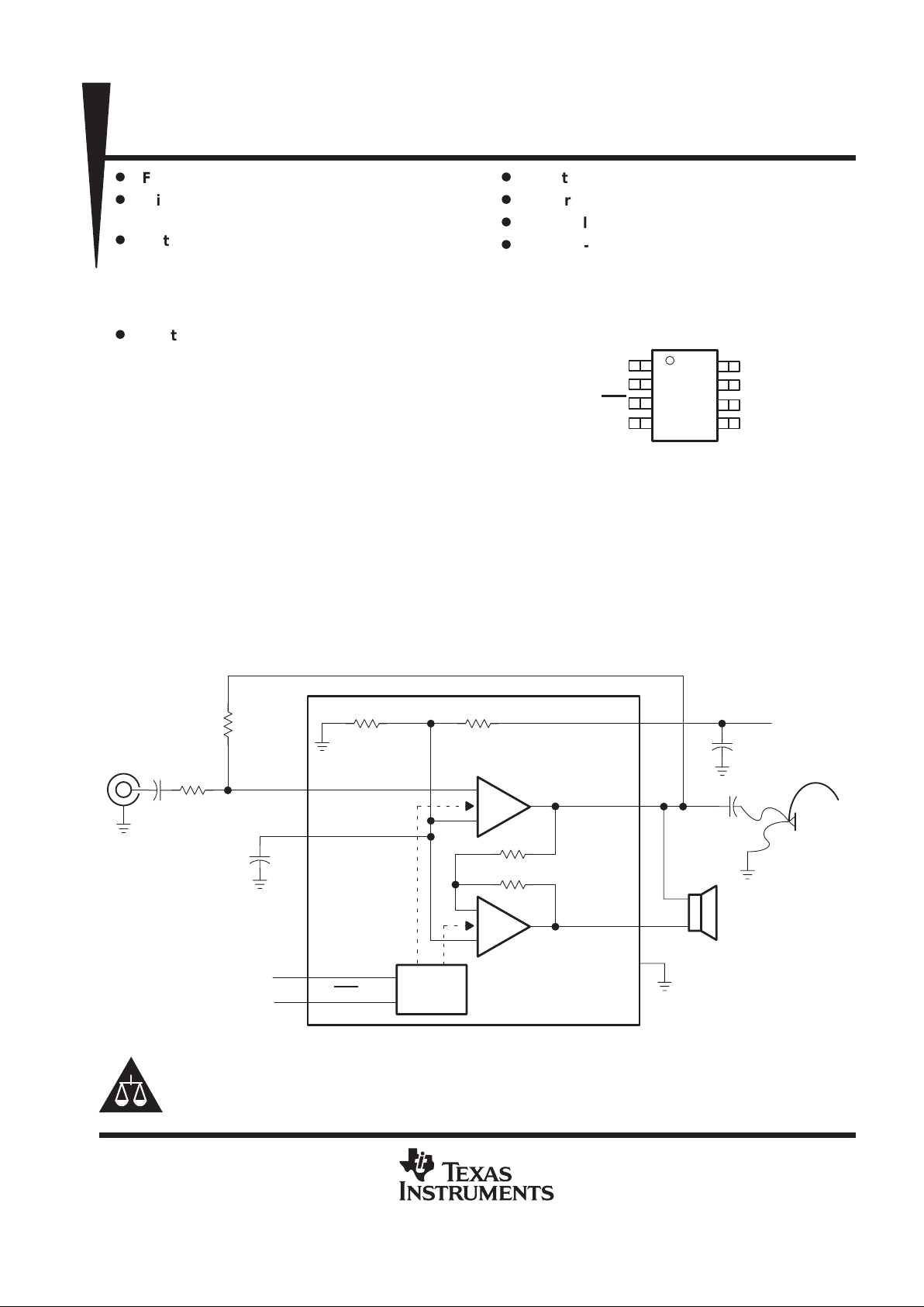
description
The TPA711 is a bridge-tied load (BTL) or
single-ended (SE) audio power amplifier developed especially for low-voltage applicationswhere internal speakers and external earphone operation are
required. Operating with a 3.3-V supply , the TPA711 can deliver 250-mW of continuous power into a BTL 8-Ω
load at less than 0.6% THD+N throughout voice band frequencies. Although this device is characterized out
to 20 kHz, its operation was optimized for narrower band applications such as wireless communications. The
BTL configuration eliminates the need for external coupling capacitors on the output in most applications, which
is particularly important for small battery-powered equipment. A unique feature of the TP A711 is that it allows
the amplifier to switch from BTL to SE
on the fly
when an earphone drive is required. This eliminates complicated
mechanical switching or auxiliary devices just to drive the external load. This device features a shutdown mode
for power-sensitive applications with special depop circuitry to eliminate speaker noise when exiting shutdown
mode. The TPA711 is available in an 8-pin SOIC and the surface-mount PowerPAD MSOP package, which
reduces board space by 50% and height by 40%.
Audio
Input
Bias
Control
V
DD
700 mW
6
5
7
VO+
V
DD
3
1
24BYPASS
IN
SE/BTL
VDD/2
C
I
R
I
C
S
C
B
R
F
SHUTDOWN
From HP Jack
VO–8
GND
From System Control
–
+
–
+
Please be aware that an important notice concerning availability, standard warranty, and use in critical applications of
Texas Instruments semiconductor products and disclaimers thereto appears at the end of this data sheet.
Copyright 2000, Texas Instruments Incorporated
PRODUCTION DATA information is current as of publication date.
Products conform to specifications per the terms of Texas Instruments
standard warranty. Production processing does not necessarily include
testing of all parameters.
1
2
3
4
8
7
6
5
SHUTDOWN
BYPASS
SE/BTL
IN
V
O
–
GND
V
DD
VO+
D OR DGN PACKAGE
(TOP VIEW)
PowerPAD is a trademark of Texas Instruments.
TPA711
700-mW MONO LOW-VOLTAGE AUDIO POWER AMPLIFIER
SLOS230B – NOVEMBER 1998 – REVISED MARCH 2000
2
POST OFFICE BOX 655303 • DALLAS, TEXAS 75265
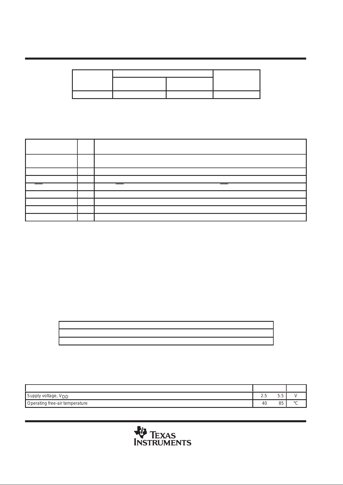
AVAILABLE OPTIONS
PACKAGED DEVICES
T
A
SMALL OUTLINE
†
(D)
MSOP
‡
(DGN)
MSOP
SYMBOLIZATION
–40°C to 85°C TPA711D TPA711DGN ABB
†
In the SOIC package, the maximum RMS output power is thermally limited to 350 mW; 700 mW
peaks can be driven, as long as the RMS value is less than 350 mW.
‡
The D and DGN packages are available taped and reeled. T o order a taped and reeled part, add
the suffix R to the part number (e.g., TP A311DR).
Terminal Functions
TERMINAL
NAME NO.
I/O
DESCRIPTION
BYPASS 2 I
BYPASS is the tap to the voltage divider for internal mid-supply bias. This terminal should be connected to
a 0.1-µF to 2.2-µF capacitor when used as an audio amplifier.
GND 7 GND is the ground connection.
IN 4 I IN is the audio input terminal.
SE/BTL 3 I When SE/BTL is held low, the TP A71 1 is in BTL mode. When SE/BTL is held high, the TP A711 is in SE mode.
SHUTDOWN 1 I SHUTDOWN places the entire device in shutdown mode when held high (IDD = 7 µA).
V
DD
6 VDD is the supply voltage terminal.
VO+ 5 O VO+ is the positive output for BTL and SE modes.
VO– 8 O VO– is the negative output in BTL mode and a high-impedance output in SE mode.
absolute maximum ratings over operating free-air temperature range (unless otherwise noted)
§
Supply voltage, VDD 6 V. . . . . . . . . . . . . . . . . . . . . . . . . . . . . . . . . . . . . . . . . . . . . . . . . . . . . . . . . . . . . . . . . . . . . . . .
Input voltage, VI –0.3 V to VDD +0.3 V. . . . . . . . . . . . . . . . . . . . . . . . . . . . . . . . . . . . . . . . . . . . . . . . . . . . . . . . . . . .
Continuous total power dissipation internally limited (see Dissipation Rating Table). . . . . . . . . . . . . . . . . . . . .
Operating free-air temperature range, T
A
(see Table 3) –40°C to 85°C. . . . . . . . . . . . . . . . . . . . . . . . . . . . . . . .
Operating junction temperature range, TJ –40°C to 150°C. . . . . . . . . . . . . . . . . . . . . . . . . . . . . . . . . . . . . . . . . . .
Storage temperature range, T
stg
–65°C to 150°C. . . . . . . . . . . . . . . . . . . . . . . . . . . . . . . . . . . . . . . . . . . . . . . . . . .
Lead temperature 1,6 mm (1/16 inch) from case for 10 seconds 260°C. . . . . . . . . . . . . . . . . . . . . . . . . . . . . . .
§
Stresses beyond those listed under “absolute maximum ratings” may cause permanent damage to the device. These are stress ratings only, and
functional operation of the device at these or any other conditions beyond those indicated under “recommended operating conditions” is not
implied. Exposure to absolute-maximum-rated conditions for extended periods may affect device reliability.
DISSIPATION RATING TABLE
PACKAGE
TA ≤ 25°C DERA TING FACTOR TA = 70°C TA = 85°C
D 725 mW 5.8 mW/°C 464 mW 377 mW
DGN 2.14 W
¶
17.1 mW/°C 1.37 W 1.11 W
¶
Please see the Texas Instruments document,
PowerPAD Thermally Enhanced Package Application Report
(literature number SLMA002), for more information on the PowerPAD package. The thermal data was
measured on a PCB layout based on the information in the section entitled
T exas Instruments Recommended
Board for PowerPAD
on page 33 of the before mentioned document.
recommended operating conditions
MIN MAX UNIT
Supply voltage, V
DD
2.5
5.5
V
Operating free-air temperature, TA (see Table 3)
–40
85
°C
TPA711
700-mW MONO LOW-VOLTAGE AUDIO POWER AMPLIFIER
SLOS230B – NOVEMBER 1998 – REVISED MARCH 2000
3
POST OFFICE BOX 655303 • DALLAS, TEXAS 75265
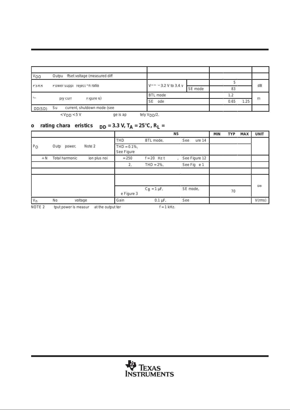
electrical characteristics at specified free-air temperature, VDD = 3.3 V , TA = 25°C (unless otherwise
noted)
PARAMETER TEST CONDITIONS
MIN TYP MAX UNIT
V
OO
ББББББББББББББ
Output offset voltage (measured differentially)
See Note 1
20
mV
ББББББББББББББ
pp
BTL mode
85
PSRR
ББББББББББББББ
Power supply rejection ratio
V
DD
= 3.2 V to 3.4
V
SE mode
83
dB
ББББББББББББББ
pp
BTL mode
1.25
2.5
I
DD
ББББББББББББББ
Supply current (see Figure 6)
SE mode
0.65
1.25
mA
I
DD(SD)
Supply current, shutdown mode (see Figure 7)
7
50
µA
NOTE 1: At 3 V < VDD < 5 V the dc output voltage is approximately VDD/2.
operating characteristics, VDD = 3.3 V, T
A
= 25°C, RL = 8 Ω
PARAMETER TEST CONDITIONS
MIN TYP MAX UNIT
БББББББББ
THD = 0.2%,
BTL mode,
See Figure 14
250
P
O
БББББББББ
Output power, see Note 2
THD = 0.1%,
See Figure 22
SE mode,
RL = 32 Ω,
37
mW
THD + N
БББББББББ
Total harmonic distortion plus noise
PO = 250 mW,
f = 200 Hz to 4 kHz,
See Figure 12
0.55%
B
OM
БББББББББ
Maximum output power bandwidth
Gain = 2,
THD = 2%,
See Figure 12
20
kHz
B
1
БББББББББ
Unity-gain bandwidth
Open Loop,
See Figure 36
1.4
MHz
ÁÁ
Á
БББББББББ
ББББББББ
Á
pp
pp
ÁÁÁ
Á
f = 1 kHz,
See Figure 5
ÁÁÁÁ
Á
CB = 1 µF,
ÁÁÁ
Á
BTL mode,
ÁÁÁ
Á
79
ÁÁÁ
Á
Supply ripple rejection ratio
f = 1 kHz,
See Figure 3
CB = 1 µF,
SE mode,
70
dB
V
n
Noise output voltage
Gain = 1,
CB = 0.1 µF,
See Figure 42
17
µV(rms)
NOTE 2: Output power is measured at the output terminals of the device at f = 1 kHz.
TPA711
700-mW MONO LOW-VOLTAGE AUDIO POWER AMPLIFIER
SLOS230B – NOVEMBER 1998 – REVISED MARCH 2000
4
POST OFFICE BOX 655303 • DALLAS, TEXAS 75265
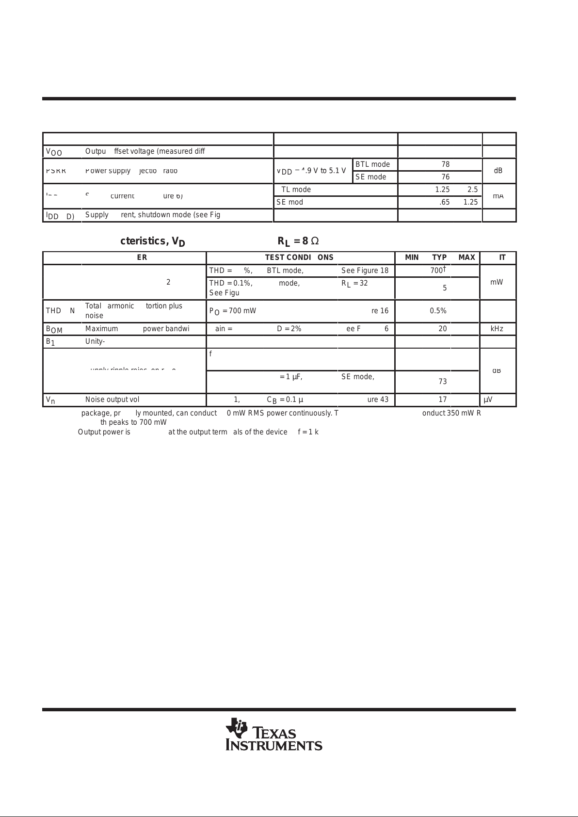
electrical characteristics at specified free-air temperature, VDD = 5 V , TA = 25°C (unless otherwise
noted)
PARAMETER TEST CONDITIONS
MIN TYP MAX UNIT
V
OO
Output offset voltage (measured differentially)
20
mV
pp
BTL mode
78
PSRR
Power supply rejection ratio
V
DD
= 4.9 V to 5.1
V
SE mode
76
dB
pp
BTL mode
1.25
2.5
IDDSupply current (see Figure 6)
SE mode
0.65
1.25
mA
I
DD(SD)
Supply current, shutdown mode (see Figure 7)
50
100
µA
operating characteristics, VDD = 5 V, T
A
= 25°C, RL = 8 Ω
PARAMETER TEST CONDITIONS
MIN TYP MAX UNIT
THD = 0.3%,
BTL mode,
See Figure 18
700
†
ÁÁ
Á
P
O
ББББББББ
Á
Output power, see Note 2
ÁÁÁ
Á
THD = 0.1%,
See Figure 26
ÁÁÁÁ
Á
SE mode,
ÁÁÁ
Á
RL = 32 Ω,
ÁÁÁ
Á
85
ÁÁÁ
Á
mW
THD + N
Total harmonic distortion plus
noise
PO = 700 mW,
f = 200 Hz to 4 kHz,
See Figure 16
0.5%
B
OM
Maximum output power bandwidth
Gain = 2,
THD = 2%,
See Figure 16
20
kHz
B
1
Unity-gain bandwidth
Open Loop,
See Figure 37
1.4
MHz
ÁÁÁББББББББ
Á
pp
pp
ÁÁÁ
Á
f = 1 kHz,
See Figure 5
ÁÁÁÁ
Á
CB = 1 µF,
ÁÁÁ
Á
BTL mode,
ÁÁÁ
Á
80
ÁÁÁ
Á
Supply ripple rejection ratio
f = 1 kHz,
See Figure 4
CB = 1 µF,
SE mode,
73
dB
V
n
Noise output voltage
Gain = 1,
CB = 0.1 µF,
See Figure 43
17
µV(rms)
†
The DGN package, properly mounted, can conduct 700 mW RMS power continuously. The D package, can only conduct 350 mW RMS power
continuously , with peaks to 700 mW.
NOTE 2: Output power is measured at the output terminals of the device at f = 1 kHz.
TPA711
700-mW MONO LOW-VOLTAGE AUDIO POWER AMPLIFIER
SLOS230B – NOVEMBER 1998 – REVISED MARCH 2000
5
POST OFFICE BOX 655303 • DALLAS, TEXAS 75265
PARAMETER MEASUREMENT INFORMATION
Audio
Input
Bias
Control
V
DD
6
5
7
VO+
V
DD
3
1
24BYPASS
IN
SE/BTL
VDD/2
C
I
R
I
C
S
C
B
R
F
SHUTDOWN
VO–8
RL = 8
Ω
GND
–
+
–
+
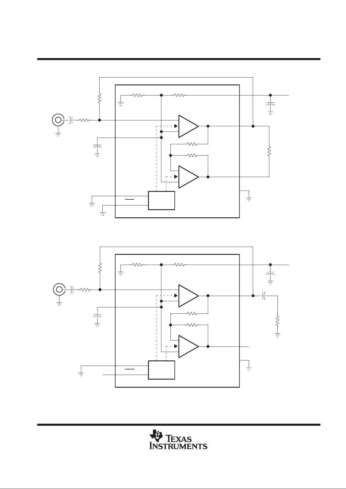
Figure 1. BTL Mode Test Circuit
Audio
Input
Bias
Control
V
DD
6
5
7
VO+
V
DD
3
1
24BYPASS
IN
SE/BTL
VDD/2
C
I
R
I
C
S
C
B
R
F
SHUTDOWN
VO–8
RL = 32
Ω
GND
C
O
V
DD
–
+
–
+
Figure 2. SE Mode Test Circuit
TPA711
700-mW MONO LOW-VOLTAGE AUDIO POWER AMPLIFIER
SLOS230B – NOVEMBER 1998 – REVISED MARCH 2000
6
POST OFFICE BOX 655303 • DALLAS, TEXAS 75265
TYPICAL CHARACTERISTICS
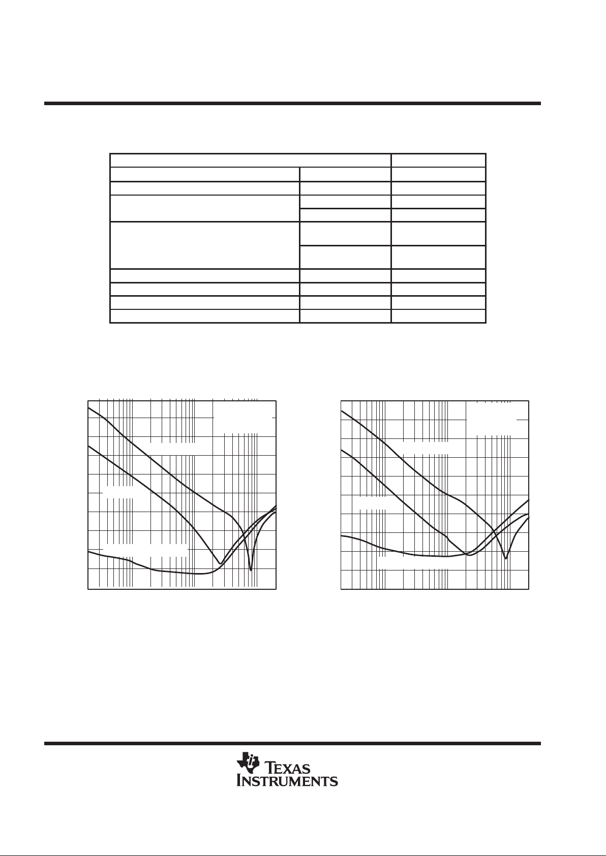
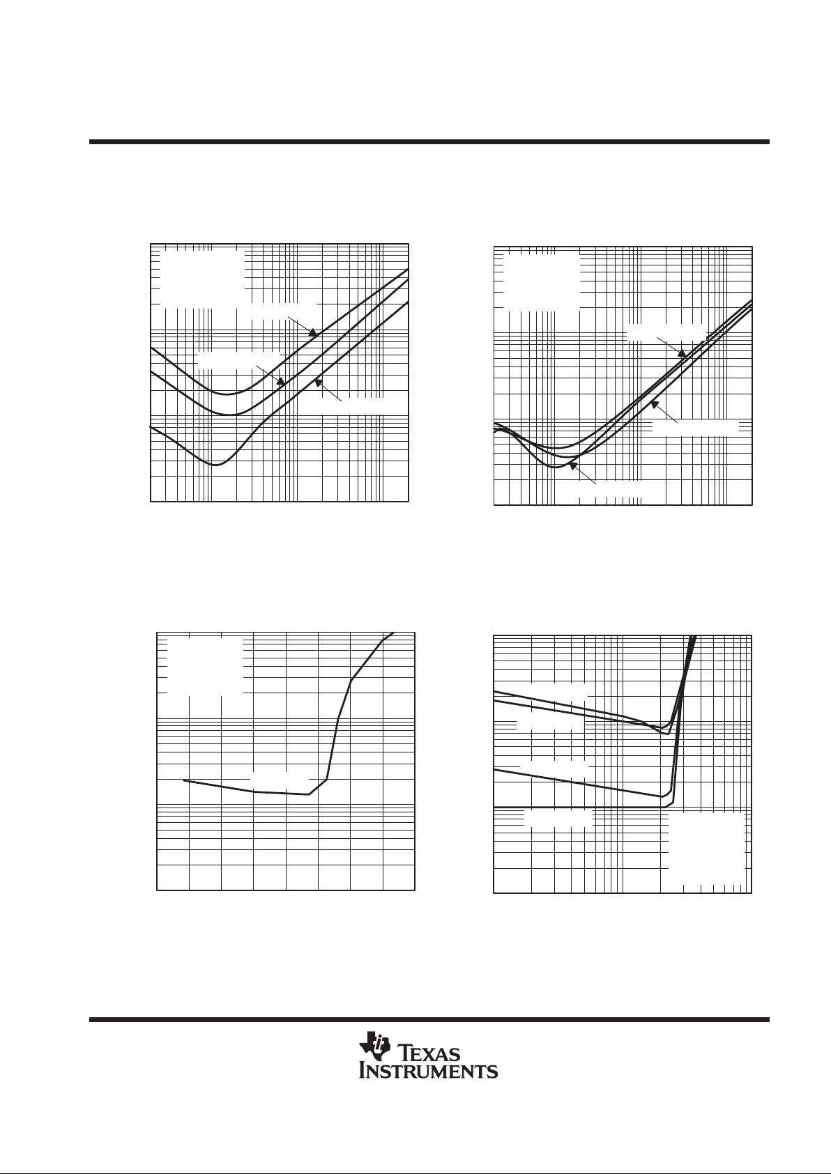
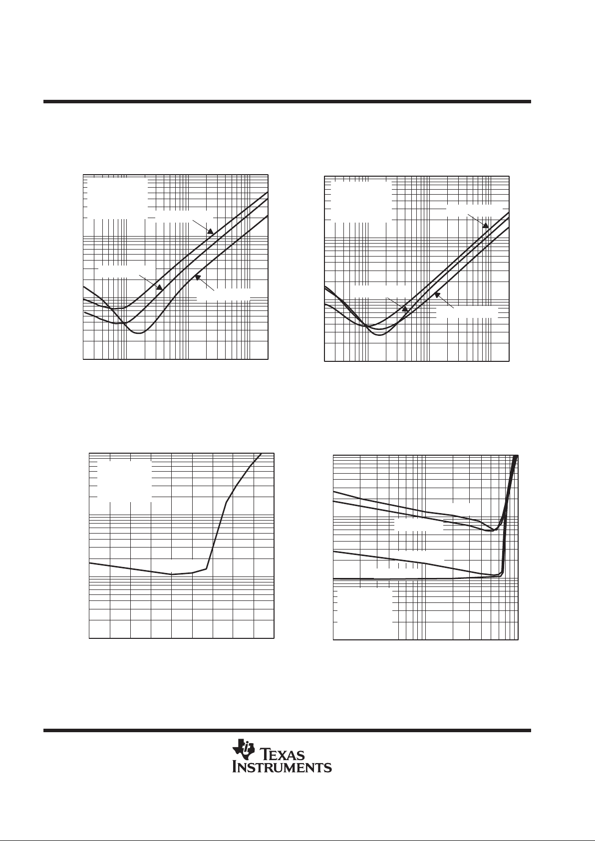
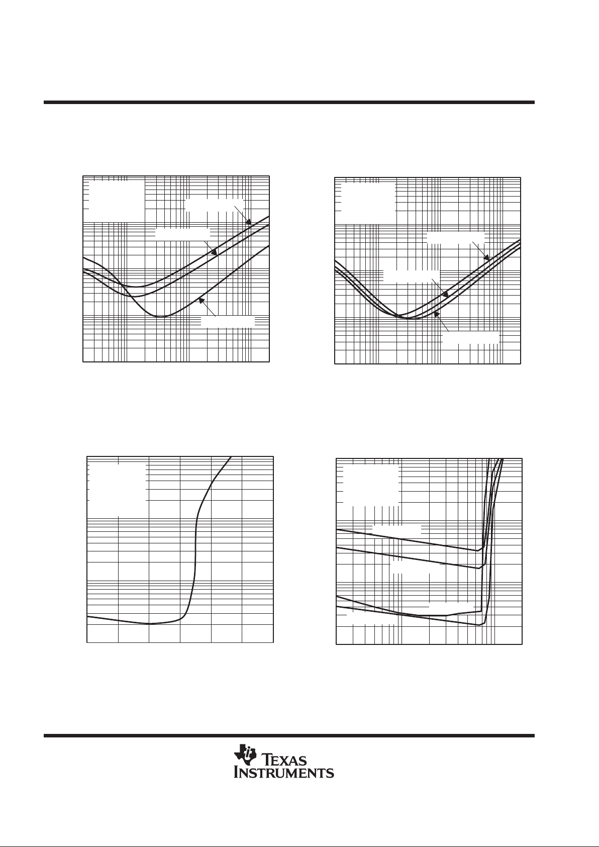
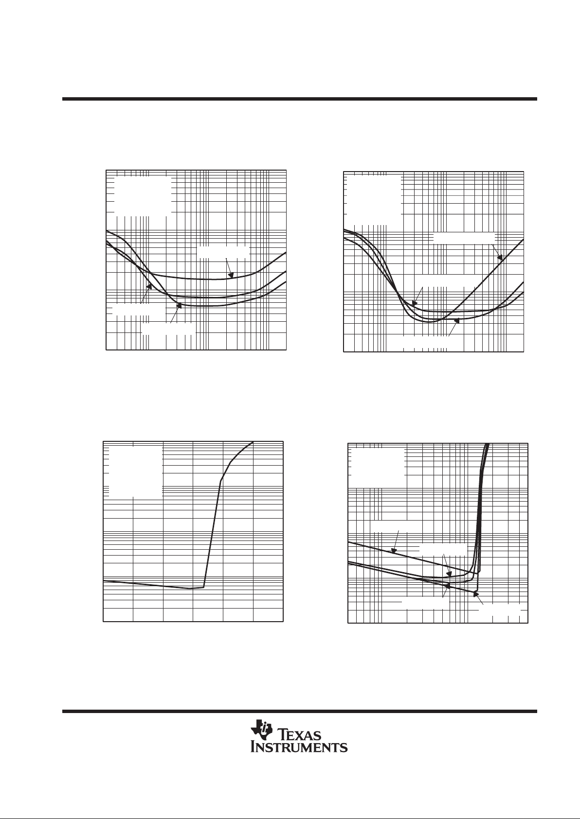
Table of Graphs
FIGURE
Supply ripple rejection ratio vs Frequency 3, 4, 5
I
DD
Supply current vs Supply voltage 6, 7
p
p
vs Supply voltage 8, 9
POOutput power
vs Load resistance 10, 11
p
vs Frequency
12, 13, 16, 17, 20, 21,
24, 25, 28, 29, 32, 33
THD+N
Total harmonic distortion plus noise
vs Output power
14, 15, 18, 19, 22, 23,
26, 27, 30, 31, 34, 35
Open loop gain and phase vs Frequency 36, 37
Closed loop gain and phase vs Frequency 38, 39, 40, 41
V
n
Output noise voltage vs Frequency 42, 43
P
D
Power dissipation vs Output power 44, 45, 46, 47
Figure 3
–50
–60
–80
–100
20 100 1k
–30
–20
f – Frequency – Hz
SUPPLY RIPPLE REJECTION RATIO
vs
FREQUENCY
0
10k 20k
–10
–40
–70
–90
BYPASS = 1/2 V
DD
CB = 0.1 µF
VDD = 3.3 V
RL = 8 Ω
SE
CB = 1 µF
Supply Ripple Rejection Ratio – dB
Figure 4
–50
–60
–80
–100
20 100 1k
–30
–20
f – Frequency – Hz
SUPPLY RIPPLE REJECTION RATIO
vs
FREQUENCY
0
10k 20k
–10
–40
–70
–90
BYPASS = 1/2 V
DD
CB = 0.1 µF
VDD = 5 V
RL = 8 Ω
SE
CB = 1 µF
Supply Ripple Rejection Ratio – dB
TPA711
700-mW MONO LOW-VOLTAGE AUDIO POWER AMPLIFIER
SLOS230B – NOVEMBER 1998 – REVISED MARCH 2000
7
POST OFFICE BOX 655303 • DALLAS, TEXAS 75265
TYPICAL CHARACTERISTICS
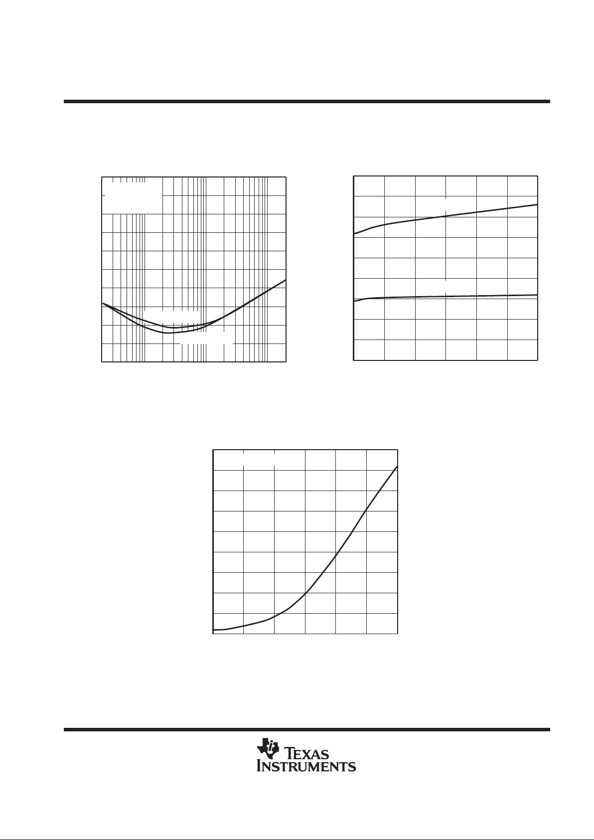
Figure 5
–50
–60
–80
–100
20 100 1k
–30
–20
f – Frequency – Hz
SUPPLY RIPPLE REJECTION RATIO
vs
FREQUENCY
0
10k 20k
–10
–40
–70
–90
VDD = 5 V
VDD = 3.3 V
RL = 8 Ω
CB = 1 µF
BTL
Supply Ripple Rejection Ratio – dB
Figure 6
VDD – Supply Voltage – V
SUPPLY CURRENT
vs
SUPPLY VOLTAGE
1.8
1.4
0.4
0
1.6
1.2
0.2
3 3.5 5.5
4.5
I
DD
– Supply Current – mA
42.5 5
0.8
0.6
1
SE
BTL
2.5
VDD – Supply Voltage – V
SUPPLY CURRENT
vs
SUPPLY VOLTAGE
20
10
0
343.5 4.5
60
5
30
SHUTDOWN = High
40
50
5.5
I
DD
– Supply Current – Aµ
70
80
90
Figure 7
TPA711
700-mW MONO LOW-VOLTAGE AUDIO POWER AMPLIFIER
SLOS230B – NOVEMBER 1998 – REVISED MARCH 2000
8
POST OFFICE BOX 655303 • DALLAS, TEXAS 75265
TYPICAL CHARACTERISTICS
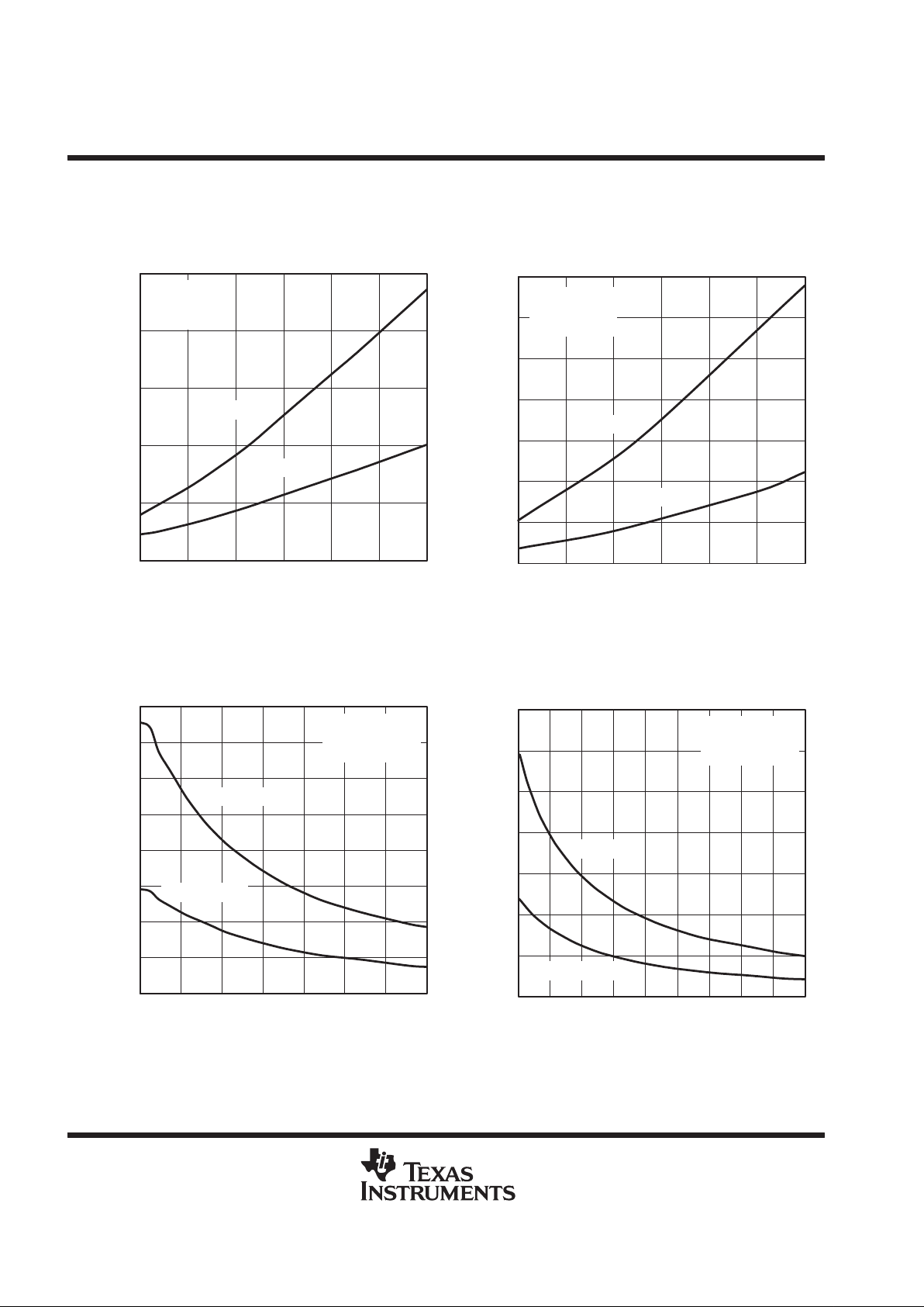
Figure 8
VDD – Supply Voltage – V
OUTPUT POWER
vs
SUPPLY VOLTAGE
600
400
200
0
2.5 3.53 4 5.5
1000
P
4.5 5
O
– Output Power – mW
800
THD+N 1%
f = 1 kHz
BTL
RL = 32 Ω
RL = 8 Ω
Figure 9
VDD – Supply Voltage – V
OUTPUT POWER
vs
SUPPLY VOLTAGE
150
100
50
0
343.5 4.5
350
P
5
O
– Output Power – mW
200
THD+N = 1%
f = 1 kHz
SE
RL = 32 Ω
RL = 8 Ω
250
300
5.52.5
Figure 10
RL – Load Resistance – Ω
OUTPUT POWER
vs
LOAD RESISTANCE
300
200
100
0
16 3224 40 64
800
8
P
48 56
O
– Output Power – mW
400
THD+N = 1%
f = 1 kHz
BTL
VDD = 5 V
500
600
VDD = 3.3 V
700
Figure 11
RL – Load Resistance – Ω
OUTPUT POWER
vs
LOAD RESISTANCE
14 2620 32 5083844
THD+N = 1%
f = 1 kHz
SE
VDD = 5 V
VDD = 3.3 V
56 62
150
100
50
0
350
P
O
– Output Power – mW
200
250
300
TPA711
700-mW MONO LOW-VOLTAGE AUDIO POWER AMPLIFIER
SLOS230B – NOVEMBER 1998 – REVISED MARCH 2000
9
POST OFFICE BOX 655303 • DALLAS, TEXAS 75265
TYPICAL CHARACTERISTICS
Figure 12
f – Frequency – Hz
THD+N –Total Harmonic Distortion + Noise – %
TOTAL HARMONIC DISTORTION PLUS NOISE
vs
FREQUENCY
AV = –2 V/V
VDD = 3.3 V
PO = 250 mW
RL = 8 Ω
BTL
20 1k 10k
1
0.01
10
0.1
20k100
AV =– 20 V/V
AV = –10 V/V
Figure 13
f – Frequency – Hz
THD+N –Total Harmonic Distortion + Noise – %
TOTAL HARMONIC DISTORTION PLUS NOISE
vs
FREQUENCY
PO = 125 mW
VDD = 3.3 V
RL = 8 Ω
AV = –2 V/V
BTL
20 1k 10k
1
0.01
10
0.1
20k100
PO = 50 mW
PO = 250 mW
Figure 14
PO – Output Power – W
THD+N –Total Harmonic Distortion + Noise – %
TOTAL HARMONIC DISTORTION PLUS NOISE
vs
OUTPUT POWER
0 0.15 0.4
1
0.01
10
0.1
0.2 0.25 0.3 0.35
VDD = 3.3 V
f = 1 kHz
AV = –2 V/V
BTL
0.05 0.1
RL = 8 Ω
Figure 15
PO – Output Power – W
THD+N –Total Harmonic Distortion + Noise – %
TOTAL HARMONIC DISTORTION PLUS NOISE
vs
OUTPUT POWER
f = 20 kHz
VDD = 3.3 V
RL = 8 Ω
CB = 1 µF
AV = –2 V/V
BTL
0.01 0.1 1
1
0.01
10
0.1
f = 1 kHz
f = 10 kHz
f = 20 Hz
TPA711
700-mW MONO LOW-VOLTAGE AUDIO POWER AMPLIFIER
SLOS230B – NOVEMBER 1998 – REVISED MARCH 2000
10
POST OFFICE BOX 655303 • DALLAS, TEXAS 75265
TYPICAL CHARACTERISTICS
Figure 16
f – Frequency – Hz
THD+N –Total Harmonic Distortion + Noise – %
TOTAL HARMONIC DISTORTION PLUS NOISE
vs
FREQUENCY
AV = –2 V/V
VDD = 5 V
PO = 700 mW
RL = 8 Ω
BTL
20 1k 10k
1
0.01
10
0.1
20k100
AV = –20 V/V
AV = –10 V/V
Figure 17
f – Frequency – Hz
THD+N –Total Harmonic Distortion + Noise – %
TOTAL HARMONIC DISTORTION PLUS NOISE
vs
FREQUENCY
PO = 700 mW
VDD = 5 V
RL = 8 Ω
AV = –2 V/V
BTL
20 1k 10k
1
0.01
10
0.1
20k100
PO = 50 mW
PO = 350 mW
Figure 18
PO – Output Power – W
0.1 0.2 10.4 0.5 0.7 0.8
THD+N –Total Harmonic Distortion + Noise – %
TOTAL HARMONIC DISTORTION PLUS NOISE
vs
OUTPUT POWER
RL = 8 Ω
VDD = 5 V
f = 1 kHz
AV = –2 V/V
BTL
1
0.01
10
0.1
0.3 0.6 0.9
Figure 19
PO – Output Power – W
THD+N –Total Harmonic Distortion + Noise – %
TOTAL HARMONIC DISTORTION PLUS NOISE
vs
OUTPUT POWER
f = 20 Hz
VDD = 5 V
RL = 8 Ω
CB = 1 µF
AV = –2 V/V
BTL
0.01 0.1 1
1
0.01
10
0.1
f = 1 kHz
f = 10 kHz
f = 20 kHz

TPA711
700-mW MONO LOW-VOLTAGE AUDIO POWER AMPLIFIER
SLOS230B – NOVEMBER 1998 – REVISED MARCH 2000
11
POST OFFICE BOX 655303 • DALLAS, TEXAS 75265
TYPICAL CHARACTERISTICS
Figure 20
f – Frequency – Hz
THD+N –Total Harmonic Distortion + Noise – %
TOTAL HARMONIC DISTORTION PLUS NOISE
vs
FREQUENCY
AV = –10 V/V
VDD = 3.3 V
PO = 30 mW
RL = 32 Ω
SE
20 1k 10k
0.1
0.001
10
0.01
20k100
AV = –1 V/V
1
AV = –5 V/V
Figure 21
f – Frequency – Hz
THD+N –Total Harmonic Distortion + Noise – %
TOTAL HARMONIC DISTORTION PLUS NOISE
vs
FREQUENCY
VDD = 3.3 V
RL = 32 Ω
AV = –1 V/V
SE
20 1k 10k
0.1
0.001
10
0.01
20k100
PO = 10 mW
PO = 15 mW
1
PO = 30 mW
Figure 22
THD+N –Total Harmonic Distortion + Noise – %
TOTAL HARMONIC DISTORTION PLUS NOISE
vs
OUTPUT POWER
VDD = 3.3 V
f = 1 kHz
RL = 32 Ω
AV = –1 V/V
SE
1
0.01
10
0.1
PO – Output Power – W
0.02 0.025 0.050.03 0.035 0.04 0.045
Figure 23
PO – Output Power – W
THD+N –Total Harmonic Distortion + Noise – %
TOTAL HARMONIC DISTORTION PLUS NOISE
vs
OUTPUT POWER
f = 20 Hz
1
0.01
10
0.1
f = 1 kHz
f = 10 kHz
f = 20 kHz
0.002 0.10.01
VDD = 3.3 V
RL = 32 Ω
AV = –1 V/V
SE
TPA711
700-mW MONO LOW-VOLTAGE AUDIO POWER AMPLIFIER
SLOS230B – NOVEMBER 1998 – REVISED MARCH 2000
12
POST OFFICE BOX 655303 • DALLAS, TEXAS 75265
TYPICAL CHARACTERISTICS
Figure 24
f – Frequency – Hz
THD+N –Total Harmonic Distortion + Noise – %
TOTAL HARMONIC DISTORTION PLUS NOISE
vs
FREQUENCY
AV = –10 V/V
VDD = 5 V
PO = 60 mW
RL = 32 Ω
SE
20 1k 10k
0.1
0.001
10
0.01
20k100
AV = –1 V/V
1
AV = –5 V/V
Figure 25
f – Frequency – Hz
THD+N –Total Harmonic Distortion + Noise – %
TOTAL HARMONIC DISTORTION PLUS NOISE
vs
FREQUENCY
VDD = 5 V
RL = 32 Ω
AV = –1 V/V
SE
20 1k 10k
0.1
0.001
10
0.01
20k100
PO = 15 mW
PO = 60 mW
1
PO = 30 mW
Figure 26
THD+N –Total Harmonic Distortion + Noise – %
TOTAL HARMONIC DISTORTION PLUS NOISE
vs
OUTPUT POWER
VDD = 5 V
f = 1 kHz
RL = 32 Ω
AV = –1 V/V
SE
1
0.01
10
0.1
PO – Output Power – W
0.02 0.04 0.140.06 0.08 0.1 0.12
Figure 27
PO – Output Power – W
THD+N –Total Harmonic Distortion + Noise – %
TOTAL HARMONIC DISTORTION PLUS NOISE
vs
OUTPUT POWER
f = 20 Hz
VDD = 5 V
RL = 32 Ω
AV = –1 V/V
SE
1
0.01
10
0.1
f = 1 kHz
f = 10 kHz
f = 20 kHz
0.002 0.1 0.20.01
TPA711
700-mW MONO LOW-VOLTAGE AUDIO POWER AMPLIFIER
SLOS230B – NOVEMBER 1998 – REVISED MARCH 2000
13
POST OFFICE BOX 655303 • DALLAS, TEXAS 75265
TYPICAL CHARACTERISTICS
Figure 28
f – Frequency – Hz
THD+N –Total Harmonic Distortion + Noise – %
TOTAL HARMONIC DISTORTION PLUS NOISE
vs
FREQUENCY
20 1k 10k
0.1
0.001
1
20k100
0.01
VDD = 3.3 V
PO = 0.1 mW
RL = 10 kΩ
SE
AV = –5 V/V
AV = –2 V/V
AV = –1 V/V
Figure 29
f – Frequency – Hz
THD+N –Total Harmonic Distortion + Noise – %
TOTAL HARMONIC DISTORTION PLUS NOISE
vs
FREQUENCY
20 1 k 10 k
0.01
0.001
1
20 k100
0.1
VDD = 3.3 V
RL = 10 kΩ
CB = 1 µF
AV = –1 V/V
SE
PO = 0.13 mW
PO = 0.05 mW
PO = 0.1 mW
Figure 30
THD+N –Total Harmonic Distortion + Noise – %
TOTAL HARMONIC DISTORTION PLUS NOISE
vs
OUTPUT POWER
VDD = 3.3 V
f = 1 kHz
RL = 10 kΩ
AV = –1 V/V
SE
0.1
0.001
10
0.01
1
PO – Output Power – µW
50 75 200100 125 150 175
Figure 31
PO – Output Power – µW
THD+N –Total Harmonic Distortion + Noise – %
TOTAL HARMONIC DISTORTION PLUS NOISE
vs
OUTPUT POWER
f = 20 Hz
VDD = 3.3 V
RL = 10 kΩ
AV = –1 V/V
SE
f = 1 kHz
f = 10 kHz
f = 20 kHz
5 100 500
0.1
0.001
10
0.01
1
10

TPA711
700-mW MONO LOW-VOLTAGE AUDIO POWER AMPLIFIER
SLOS230B – NOVEMBER 1998 – REVISED MARCH 2000
14
POST OFFICE BOX 655303 • DALLAS, TEXAS 75265
TYPICAL CHARACTERISTICS
Figure 32
f – Frequency – Hz
THD+N –Total Harmonic Distortion + Noise – %
TOTAL HARMONIC DISTORTION PLUS NOISE
vs
FREQUENCY
VDD = 5 V
PO = 0.3 mW
RL = 10 kΩ
SE
20 1k 10k
0.01
0.001
1
20k100
AV = –1 V/V
AV = –2 V/V
AV = –5 V/V
0.1
Figure 33
f – Frequency – Hz
THD+N –Total Harmonic Distortion + Noise – %
TOTAL HARMONIC DISTORTION PLUS NOISE
vs
FREQUENCY
20 1k 10k
0.01
0.001
1
20k100
0.1
VDD = 5 V
RL = 10 kΩ
AV = –1 V/V
SE
PO = 0.1 mW
PO = 0.3 mW
PO = 0.2 mW
Figure 34
THD+N –Total Harmonic Distortion + Noise – %
TOTAL HARMONIC DISTORTION PLUS NOISE
vs
OUTPUT POWER
VDD = 5 V
f = 1 kHz
RL = 10 kΩ
AV = –1 V/V
SE
0.1
0.001
10
0.01
1
PO – Output Power – µW
50 100 500150 200 250 300
350 400 450
Figure 35
PO – Output Power – µW
THD+N –Total Harmonic Distortion + Noise – %
TOTAL HARMONIC DISTORTION PLUS NOISE
vs
OUTPUT POWER
f = 20 Hz
VDD = 5 V
RL = 10 kΩ
AV = –1 V/V
SE
f = 10 kHz
5 100 500
0.1
0.001
10
0.01
1
10
f = 1 kHz
f = 20 kHz

TPA711
700-mW MONO LOW-VOLTAGE AUDIO POWER AMPLIFIER
SLOS230B – NOVEMBER 1998 – REVISED MARCH 2000
15
POST OFFICE BOX 655303 • DALLAS, TEXAS 75265
TYPICAL CHARACTERISTICS
10
0
–20
–30
20
30
f – Frequency – kHz
80
–10
180°
–180°
Phase
60°
–60°
OPEN-LOOP GAIN AND PHASE
vs
FREQUENCY
Open-Loop Gain – dB
Phase
1
10
1
10
2
10
3
10
4
50
40
60
70
140°
100°
20°
–20°
–100°
–140°
VDD = 3.3 V
RL = Open
BTL
Gain
Figure 36
10
0
–20
–30
1
20
30
f – Frequency – kHz
80
–10
Gain
Phase
OPEN-LOOP GAIN AND PHASE
vs
FREQUENCY
Open-Loop Gain – dB
10
1
10
2
10
3
10
4
50
40
60
70
VDD = 5 V
RL = Open
BTL
180°
–180°
60°
–60°
Phase
140°
100°
20°
–20°
–100°
–140°
Figure 37

TPA711
700-mW MONO LOW-VOLTAGE AUDIO POWER AMPLIFIER
SLOS230B – NOVEMBER 1998 – REVISED MARCH 2000
16
POST OFFICE BOX 655303 • DALLAS, TEXAS 75265
TYPICAL CHARACTERISTICS
CLOSED-LOOP GAIN AND PHASE
vs
FREQUENCY
–0.5
–1
–1.5
–2
f – Frequency – Hz
–0.25
–0.75
–1.25
–1.75
0
0.5
Closed-Loop Gain – dB
0.25
0.75
130°
120°
140°
Phase
150°
160°
VDD = 3.3 V
RL = 8 Ω
PO = 250 mW
BTL
1
170°
180°
Gain
Phase
10
1
10
2
10
3
10
4
10
5
10
6
Figure 38
CLOSED-LOOP GAIN AND PHASE
vs
FREQUENCY
–0.5
–1
–1.5
–2
f – Frequency – Hz
–0.25
–0.75
–1.25
–1.75
0
0.5
Closed-Loop Gain – dB
0.25
0.75
130°
120°
140°
Phase
150°
160°
VDD = 5 V
RL = 8 Ω
PO = 700 m W
BTL
1
170°
180°
Gain
Phase
10
1
10
2
10
3
10
4
10
5
10
6
Figure 39

TPA711
700-mW MONO LOW-VOLTAGE AUDIO POWER AMPLIFIER
SLOS230B – NOVEMBER 1998 – REVISED MARCH 2000
17
POST OFFICE BOX 655303 • DALLAS, TEXAS 75265
TYPICAL CHARACTERISTICS
CLOSED-LOOP GAIN AND PHASE
vs
FREQUENCY
3
1
–1
–2
f – Frequency – Hz
4
2
0
5
7
Closed-Loop Gain – dB
6
VDD = 3.3 V
RL = 32 Ω
AV = 2 V/V
PO = 30 mW
SE
Gain
Phase
110°
100°
120°
Phase
130°
140°
150°
180°
160°
170°
10
1
10
2
10
3
10
4
10
5
10
6
Figure 40
CLOSED-LOOP GAIN AND PHASE
vs
FREQUENCY
4
2
0
–2
f – Frequency – Hz
5
3
1
–1
6
Closed-Loop Gain – dB
7
110°
100°
120°
Phase
130°
140°
VDD = 5 V
RL = 32 Ω
AV = 2 V/V
PO = 60 mW
SE
150°
180°
Gain
Phase
160°
170°
10
1
10
2
10
3
10
4
10
5
10
6
Figure 41

TPA711
700-mW MONO LOW-VOLTAGE AUDIO POWER AMPLIFIER
SLOS230B – NOVEMBER 1998 – REVISED MARCH 2000
18
POST OFFICE BOX 655303 • DALLAS, TEXAS 75265
TYPICAL CHARACTERISTICS
Figure 42
– Output Noise Voltage – VµV
n
f – Frequency – Hz
OUTPUT NOISE VOLTAGE
vs
FREQUENCY
20 1 k 10 k
10
1
100
20 k100
VO BTL
VDD = 3.3 V
BW = 22 Hz to 22 kHz
RL = 8 Ω or 32 Ω
AV = 1
V
O+
(rms)
Figure 43
– Output Noise Voltage – VµV
n
f – Frequency – Hz
OUTPUT NOISE VOLTAGE
vs
FREQUENCY
20 1 k 10 k
10
1
100
20 k100
VDD = 5 V
BW = 22 Hz to 22 kHz
RL = 8 Ω or 32 Ω
AV = 1
VO BTL
V
O+
(rms)
Figure 44
PD – Output Power – mW
POWER DISSIPATION
vs
OUTPUT POWER
400 6000
150
100
50
0
350
P
D
– Power Dissipation – mW
200
250
300
200
VDD = 3.3 V
BTL
RL = 32 Ω
RL = 8 Ω
Figure 45
PD – Output Power – W
POWER DISSIPATION
vs
OUTPUT POWER
1500
30
20
10
0
70
P
D
– Power Dissipation – mW
40
50
60
100
80
90
50 100
VDD = 3.3 V
SE
RL = 32 Ω
RL = 8 Ω

TPA711
700-mW MONO LOW-VOLTAGE AUDIO POWER AMPLIFIER
SLOS230B – NOVEMBER 1998 – REVISED MARCH 2000
19
POST OFFICE BOX 655303 • DALLAS, TEXAS 75265
TYPICAL CHARACTERISTICS
Figure 46
PD – Output Power – mW
POWER DISSIPATION
vs
OUTPUT POWER
200 600400 8000 1000
400
300
100
0
800
P
D
– Power Dissipation – mW
500
600
700
200
VDD = 5 V
BTL
RL = 32 Ω
RL = 8 Ω
Figure 47
PD – Output Power – mW
POWER DISSIPATION
vs
OUTPUT POWER
50 150100 2000 250 300
100
80
60
0
200
P
D
– Power Dissipation – mW
120
140
160
20
40
180
VDD = 5 V
SE
RL = 8 Ω
RL = 32 Ω
TPA711
700-mW MONO LOW-VOLTAGE AUDIO POWER AMPLIFIER
SLOS230B – NOVEMBER 1998 – REVISED MARCH 2000
20
POST OFFICE BOX 655303 • DALLAS, TEXAS 75265
APPLICATION INFORMATION
bridged-tied load versus single-ended mode
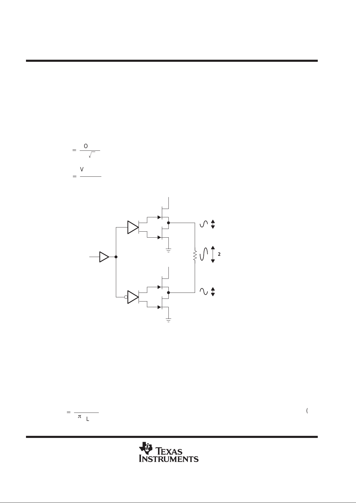
Figure 48 shows a linear audio power amplifier (AP A) in a BTL configuration. The TPA71 1 BTL amplifier consists
of two linear amplifiers driving both ends of the load. There are several potential benefits to this differential drive
configuration but initially consider power to the load. The differential drive to the speaker means that as one side
is slewing up, the other side is slewing down, and vice versa. This in effect doubles the voltage swing on the
load as compared to a ground referenced load. Plugging 2 × V
O(PP)
into the power equation, where voltage is
squared, yields 4× the output power from the same supply rail and load impedance (see equation 1).
Power
+
V
(rms)
2
R
L
(1)
V
(rms)
+
V
O(PP)
22
Ǹ
R
L
2x V
O(PP)
V
O(PP)
–V
O(PP)
V
DD
V
DD
Figure 48. Bridge-Tied Load Configuration
In a typical portable handheld equipment sound channel operating at 3.3 V, bridging raises the power into an
8-Ω speaker from a singled-ended (SE, ground reference) limit of 62.5 mW to 250 mW. In sound power that is
a 6-dB improvement, which is loudness that can be heard. In addition to increased power there are frequency
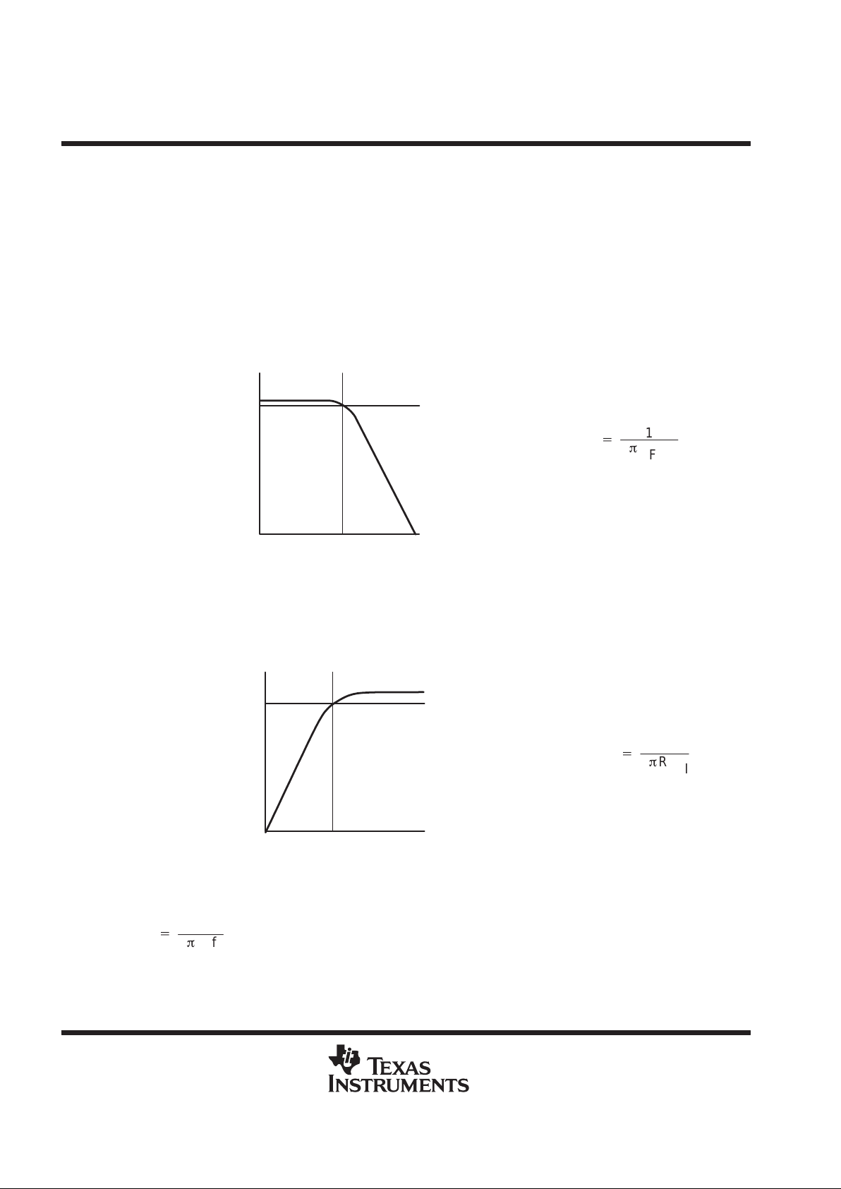
response concerns. Consider the single-supply SE configuration shown in Figure 49. A coupling capacitor is
required to block the dc offset voltage from reaching the load. These capacitors can be quite large
(approximately 33 µF to 1000 µF) so they tend to be expensive, heavy, occupy valuable PCB area, and have
the additional drawback of limiting low-frequency performance of the system. This frequency limiting effect is
due to the high pass filter network created with the speaker impedance and the coupling capacitance and is
calculated with equation 2.
fc+
1
2pRLC
C
(2)

TPA711
700-mW MONO LOW-VOLTAGE AUDIO POWER AMPLIFIER
SLOS230B – NOVEMBER 1998 – REVISED MARCH 2000
21
POST OFFICE BOX 655303 • DALLAS, TEXAS 75265
APPLICATION INFORMATION
bridged-tied load versus single-ended mode (continued)
For example, a 68-µF capacitor with an 8-Ω speaker would attenuate low frequencies below 293 Hz. The BTL
configuration cancels the dc offsets, which eliminates the need for the blocking capacitors. Low-frequency
performance is then limited only by the input network and speaker response. Cost and PCB space are also
minimized by eliminating the bulky coupling capacitor.
R
L
C
C
V
O(PP)
V
O(PP)
V
DD
–3 dB
f
c
Figure 49. Single-Ended Configuration and Frequency Response
Increasing power to the load does carry a penalty of increased internal power dissipation. The increased
dissipation is understandable considering that the BTL configuration produces 4× the output power of the SE
configuration. Internal dissipation versus output power is discussed further in the
thermal considerations
section.
BTL amplifier efficiency
Linear amplifiers are notoriously inefficient. The primary cause of these inefficiencies is voltage drop across the
output stage transistors. There are two components of the internal voltage drop. One is the headroom or dc
voltage drop that varies inversely to output power. The second component is due to the sinewave nature of the
output. The total voltage drop can be calculated by subtracting the RMS value of the output voltage from V
DD
.
The internal voltage drop multiplied by the RMS value of the supply current, IDDrms, determines the internal
power dissipation of the amplifier.
An easy-to-use equation to calculate efficiency starts out being equal to the ratio of power from the power supply
to the power delivered to the load. To accurately calculate the RMS values of power in the load and in the
amplifier, the current and voltage waveform shapes must first be understood (see Figure 50).
V
(LRMS)
V
O
I
DD
I
DD(RMS)
Figure 50. Voltage and Current Waveforms for BTL Amplifiers

TPA711
700-mW MONO LOW-VOLTAGE AUDIO POWER AMPLIFIER
SLOS230B – NOVEMBER 1998 – REVISED MARCH 2000
22
POST OFFICE BOX 655303 • DALLAS, TEXAS 75265
APPLICATION INFORMATION
BTL amplifier efficiency (continued)
Although the voltages and currents for SE and BTL are sinusoidal in the load, currents from the supply are very
different between SE and BTL configurations. In an SE application the current waveform is a half-wave rectified
shape, whereas in BTL it is a full-wave rectified waveform. This means RMS conversion factors are different.
Keep in mind that for most of the waveform, both the push and pull transistors are not on at the same time, which
supports the fact that each amplifier in the BTL device only draws current from the supply for half the waveform.
The following equations are the basis for calculating amplifier efficiency.
IDDrms
+
2V
P
p
R
L
P
SUP
+
VDDIDDrms
+
VDD2V
P
p
R
L
Efficiency
+
P
L
P
SUP
Efficiency of a BTL Configuration
+
p
V
P
2V
DD
+
p
ǒ
PLR
L
2
Ǔ
1ń2
2V
DD
(3)
Where:
(4)
PL+
VLrms
2
R
L
+
V
p
2
2R
L
VLrms
+
V
P
2
Ǹ
T able 1 employs equation 4 to calculate efficiencies for three dif ferent output power levels. The efficiency of the
amplifier is quite low for lower power levels and rises sharply as power to the load is increased, resulting in a
nearly flat internal power dissipation over the normal operating range. The internal dissipation at full output
power is less than in the half power range. Calculating the efficiency for a specific system is the key to proper
power supply design.
Table 1. Efficiency Vs Output Power in 3.3-V 8-Ω BTL Systems
OUTPUT POWER
(W)
EFFICIENCY
(%)
PEAK-to-PEAK
VOLTAGE
(V)
INTERNAL
DISSIPATION
(W)
0.125 33.6 1.41 0.26
0.25 47.6 2.00 0.29
0.375 58.3 2.45
†
0.28
†
High-peak voltage values cause the THD to increase.
A final point to remember about linear amplifiers (either SE or BTL) is how to manipulate the terms in the
efficiency equation to utmost advantage when possible. In equation 4, VDD is in the denominator. This indicates
that as VDD goes down, efficiency goes up.

TPA711
700-mW MONO LOW-VOLTAGE AUDIO POWER AMPLIFIER
SLOS230B – NOVEMBER 1998 – REVISED MARCH 2000
23
POST OFFICE BOX 655303 • DALLAS, TEXAS 75265
APPLICATION INFORMATION
application schematic
Figure 51 is a schematic diagram of a typical handheld audio application circuit, configured for a gain of
–10 V/V.
Audio
Input
Bias
Control
V
DD
6
5
7
VO+
V
DD
3
1
24BYPASS
IN
SE/BTL
VDD/2
C
I
0.47 µF
R
I
10 kΩ
C
S
1 µF
C
B
2.2 µF
RF
50 kΩ
SHUTDOWN
VO–8
GND
From System Control
C
F
5 pF
CC
330 µF
1 kΩ
100 kΩ
V
DD
100 kΩ
–
+
–
+
0.1 µF
Figure 51. TPA711 Application Circuit
The following sections discuss the selection of the components used in Figure 51.
component selection
gain setting resistors, RF and R
I
The gain for each audio input of the TP A71 1 is set by resistors RF and RI according to equation 5 for BTL mode.
(5)
BTL Gain
+*
2
ǒ
R
F
R
I
Ǔ
BTL mode operation brings about the factor 2 in the gain equation due to the inverting amplifier mirroring the
voltage swing across the load. Given that the TPA711 is a MOS amplifier, the input impedance is very high;
consequently input leakage currents are not generally a concern, although noise in the circuit increases as the
value of R
F
increases. In addition, a certain range of RF values is required for proper start-up operation of the
amplifier. Taken together it is recommended that the effective impedance seen by the inverting node of the
amplifier be set between 5 kΩ and 20 kΩ. The effective impedance is calculated in equation 6.
(6)
Effective Impedance
+
RFR
I
RF)
R
I
TPA711
700-mW MONO LOW-VOLTAGE AUDIO POWER AMPLIFIER
SLOS230B – NOVEMBER 1998 – REVISED MARCH 2000
24
POST OFFICE BOX 655303 • DALLAS, TEXAS 75265
APPLICATION INFORMATION
component selection (continued)
As an example consider an input resistance of 10 kΩ and a feedback resistor of 50 kΩ. The BTL gain of the
amplifier would be –10 V/V and the effective impedance at the inverting terminal would be 8.3 kΩ, which is well
within the recommended range.
For high performance applications, metal film resistors are recommended because they tend to have lower
noise levels than carbon resistors. For values of RF above 50 kΩ, the amplifier tends to become unstable due
to a pole formed from RF and the inherent input capacitance of the MOS input structure. For this reason, a small
compensation capacitor of approximately 5 pF should be placed in parallel with RF when RF is greater than
50 kΩ. This, in effect, creates a low pass filter network with the cutoff frequency defined in equation 7.
(7)
–3 dB
f
c
f
c(lowpass)
+
1
2pRFC
F
For example, if RF is 100 kΩ and CF is 5 pF, then fc is 318 kHz, which is well outside of the audio range.
input capacitor, C
I
In the typical application an input capacitor, CI, is required to allow the amplifier to bias the input signal to the
proper dc level for optimum operation. In this case, C
I
and RI form a high-pass filter with the corner frequency
determined in equation 8.
(8)
f
c(highpass)
+
1
2pRIC
I
–3 dB
f
c
The value of CI is important to consider as it directly affects the bass (low frequency) performance of the circuit.
Consider the example where RI is 10 kΩ and the specification calls for a flat bass response down to 40 Hz.
Equation 8 is reconfigured as equation 9.
(9)
CI+
1
2pRIf
c

TPA711
700-mW MONO LOW-VOLTAGE AUDIO POWER AMPLIFIER
SLOS230B – NOVEMBER 1998 – REVISED MARCH 2000
25
POST OFFICE BOX 655303 • DALLAS, TEXAS 75265
APPLICATION INFORMATION
component selection (continued)
In this example, CI is 0.40 µF, so one would likely choose a value in the range of 0.47 µF to 1 µF. A further
consideration for this capacitor is the leakage path from the input source through the input network (RI, CI) and
the feedback resistor (RF) to the load. This leakage current creates a dc offset voltage at the input to the amplifier
that reduces useful headroom, especially in high gain applications. For this reason a low-leakage tantalum or
ceramic capacitor is the best choice. When polarized capacitors are used, the positive side of the capacitor
should face the amplifier input in most applications, as the dc level there is held at V
DD
/2, which is likely higher
than the source dc level. It is important to confirm the capacitor polarity in the application.
power supply decoupling, C
S
The TP A711 is a high-performance CMOS audio amplifier that requires adequate power supply decoupling to
ensure the output total harmonic distortion (THD) is as low as possible. Power supply decoupling also prevents
oscillations for long lead lengths between the amplifier and the speaker. The optimum decoupling is achieved
by using two capacitors of different types that target different types of noise on the power supply leads. For
higher frequency transients, spikes, or digital hash on the line, a good low equivalent-series-resistance (ESR)
ceramic capacitor, typically 0.1 µF placed as close as possible to the device V
DD
lead, works best. For filtering
lower-frequency noise signals, a larger aluminum electrolytic capacitor of 10 µF or greater placed near the audio
power amplifier is recommended.
midrail bypass capacitor, C
B
The midrail bypass capacitor, CB, is the most critical capacitor and serves several important functions. During
start-up or recovery from shutdown mode, CB determines the rate at which the amplifier starts up. The second
function is to reduce noise produced by the power supply caused by coupling into the output drive signal. This
noise is from the midrail generation circuit internal to the amplifier, which appears as degraded PSRR
THD + N. The capacitor is fed from a 250-kΩ source inside the amplifier. To keep the start-up pop as low as
possible, the relationship shown in equation 10 should be maintained. This insures the input capacitor is fully
charged before the bypass capacitor is fuly charged and the amplifier starts up.
(10)
10
ǒ
CB
250 kΩ
Ǔ
v
1
ǒ
RF)
R
I
Ǔ
C
I
As an example, consider a circuit where CB is 2.2 µF, CI is 0.47 µF, RF is 50 kΩ, and RI is 10 kΩ. Inserting these
values into the equation 10 we get:
18.2v35.5
which satisfies the rule. Bypass capacitor, CB, values of 0.1 µF to 2.2 µF ceramic or tantalum low-ESR capacitors
are recommended for the best THD and noise performance.
single-ended operation
In SE mode (see Figure 51), the load is driven from the primary amplifier output (VO+, terminal 5).
In SE mode the gain is set by the RF and RI resistors and is shown in equation 1 1. Since the inverting amplifier
is not used to mirror the voltage swing on the load, the factor of 2, from equation 5, is not included.
(11)
SE Gain
+*
ǒ
R
F
R
I
Ǔ

TPA711
700-mW MONO LOW-VOLTAGE AUDIO POWER AMPLIFIER
SLOS230B – NOVEMBER 1998 – REVISED MARCH 2000
26
POST OFFICE BOX 655303 • DALLAS, TEXAS 75265
APPLICATION INFORMATION
component selection (continued)
The output coupling capacitor required in single-supply SE mode also places additional constraints on the
selection of other components in the amplifier circuit. The rules described earlier still hold with the addition of
the following relationship:
(12)
10
ǒ
CB
250 kΩ
Ǔ
v
1
ǒ
RF)
R
I
Ǔ
C
I
Ơ
1
R
L
C
C
output coupling capacitor, C
C
In the typical single-supply SE configuration, an output coupling capacitor (CC) is required to block the dc bias
at the output of the amplifier, thus preventing dc currents in the load. As with the input coupling capacitor, the
output coupling capacitor and impedance of the load form a high-pass filter governed by equation 13.
(13)
f
c(high)
+
1
2pRLC
C
–3 dB
f
c
The main disadvantage, from a performance standpoint, is the load impedances are typically small, which drives
the low-frequency corner higher, degrading the bass response. Large values of CC are required to pass low
frequencies into the load. Consider the example where a C
C
of 330 µF is chosen and loads vary from 4 Ω,
8 Ω, 32 Ω, and 47 kΩ. Table 2 summarizes the frequency response characteristics of each configuration.
Table 2. Common Load Impedances Vs Low Frequency Output Characteristics in SE Mode
R
L
C
C
LOWEST FREQUENCY
8 Ω 330 µF 60 Hz
32 Ω 330 µF
15 Hz
47,000 Ω 330 µF 0.01 Hz
As Table 2 indicates, an 8-Ω load is adequate, earphone response is good, and drive into line level inputs (a
home stereo for example) is exceptional.

TPA711
700-mW MONO LOW-VOLTAGE AUDIO POWER AMPLIFIER
SLOS230B – NOVEMBER 1998 – REVISED MARCH 2000
27
POST OFFICE BOX 655303 • DALLAS, TEXAS 75265
APPLICATION INFORMATION
SE/BTL
operation
The ability of the TP A71 1 to easily switch between BTL and SE modes is one of its most important cost-saving
features. This feature eliminates the requirement for an additional earphone amplifier in applications where
internal speakers are driven in BTL mode but external earphone or speaker must be accommodated. Internal
to the TP A711, two separate amplifiers drive VO+ and VO–. The SE/BTL input (terminal 3) controls the operation
of the follower amplifier that drives V
O
– (terminal 8). When SE/BTL is held low, the amplifier is on and the TP A71 1
is in the BTL mode. When SE/BTL is held high, the VO– amplifier is in a high output impedance state, which
configures the TP A711 as an SE driver from VO+ (terminal 5). IDD is reduced by approximately one-half in SE
mode. Control of the SE/BTL input can be from a logic-level TTL source or, more typically , from a resistor divider
network as shown in Figure 52.
Bias
Control
5
7
VO+
3
1
24BYPASS
IN
SE/BTL
SHUTDOWN
VO–8
GND
C
C
1 kΩ
100 kΩ
V
DD
100 kΩ
–
+
–
+
0.1 µF
Figure 52. TPA711 Resistor Divider Network Circuit
Using a readily available 1/8-in. (3.5 mm) mono earphone jack, the control switch is closed when no plug is
inserted. When closed, the 100-kΩ/1-kΩ divider pulls the SE/BTL input low. When a plug is inserted, the 1-kΩ
resistor is disconnected and the SE/BTL input is pulled high. When the input goes high, the VO– amplifier is shut
down causing the BTL speaker to mute (virtually open-circuits the speaker). The VO+ amplifier then drives
through the output capacitor (C
C
) into the earphone jack.
using low-ESR capacitors
Low-ESR capacitors are recommended throughout this applications section. A real (as opposed to ideal)
capacitor can be modeled simply as a resistor in series with an ideal capacitor. The voltage drop across this
resistor minimizes the beneficial effects of the capacitor in the circuit. The lower the equivalent value of this
resistance the more the real capacitor behaves like an ideal capacitor.
TPA711
700-mW MONO LOW-VOLTAGE AUDIO POWER AMPLIFIER
SLOS230B – NOVEMBER 1998 – REVISED MARCH 2000
28
POST OFFICE BOX 655303 • DALLAS, TEXAS 75265
APPLICATION INFORMATION
5-V versus 3.3-V operation
The TP A711 operates over a supply range of 2.5 V to 5.5 V. This data sheet provides full specifications for 5-V
and 3.3-V operation, as these are considered to be the two most common standard voltages. There are no
special considerations for 3.3-V versus 5-V operation with respect to supply bypassing, gain setting, or stability .
The most important consideration is that of output power. Each amplifier in TPA711 can produce a maximum
voltage swing of V
DD
– 1 V. This means, for 3.3-V operation, clipping starts to occur when V
O(PP)
= 2.3 V as
opposed to V
O(PP)
= 4 V at 5 V . The reduced voltage swing subsequently reduces maximum output power into
an 8-Ω load before distortion becomes significant.
Operation from 3.3-V supplies, as can be shown from the efficiency formula in equation 4, consumes
approximately two-thirds the supply power of operation from 5-V supplies for a given output-power level.
headroom and thermal considerations
Linear power amplifiers dissipate a significant amount of heat in the package under normal operating conditions.
A typical music CD requires 12 dB to 15 dB of dynamic headroom to pass the loudest portions without distortion
as compared with the average power output. From the TP A71 1 data sheet, one can see that when the TPA711
is operating from a 5-V supply into a 8-Ω speaker that 700 mW peaks are available. Converting watts to dB:
PdB+
10Log
ǒ
P
W
P
ref
Ǔ+
10Log
ǒ
700 mW
1W
Ǔ
+
–1.5 dB
Subtracting the headroom restriction to obtain the average listening level without distortion yields:
–1.5 dB – 15 dB = –16.5 (15 dB headroom)
–1.5 dB – 12 dB = –13.5 (12 dB headroom)
–1.5 dB – 9 dB = –10.5 (9 dB headroom)
–1.5 dB – 6 dB = –7.5 (6 dB headroom)
–1.5 dB – 3 dB = –4.5 (3 dB headroom)
Converting dB back into watts:
PW+
10
PdBń10
P
ref
+
22 mW (15 dB headroom)
+
44 mW (12 dB headroom)
+
88 mW (9 dB headroom)
+
175 mW (6 dB headroom)
+
350 mW (3 dB headroom)

TPA711
700-mW MONO LOW-VOLTAGE AUDIO POWER AMPLIFIER
SLOS230B – NOVEMBER 1998 – REVISED MARCH 2000
29
POST OFFICE BOX 655303 • DALLAS, TEXAS 75265
APPLICATION INFORMATION
headroom and thermal considerations (continued)
This is valuable information to consider when attempting to estimate the heat dissipation requirements for the
amplifier system. Comparing the absolute worst case, which is 700 mW of continuous power output with 0 dB
of headroom, against 12 dB and 15 dB applications drastically affects maximum ambient temperature ratings
for the system. Using the power dissipation curves for a 5-V , 8-Ω system, the internal dissipation in the TP A71 1
and maximum ambient temperatures is shown in Table 3.
Table 3. TPA711 Power Rating, 5-V, 8-Ω, BTL
PEAK OUTPUT
AVERAGE OUTPUT
POWER
D PACKAGE
(SOIC)
DGN PACKAGE
(MSOP)
POWER
(mW)
POWER
DISSIPATION
(mW)
MAXIMUM AMBIENT
TEMPERATURE
MAXIMUM AMBIENT
TEMPERATURE
700 700 mW 675 34°C 110°C
700 350 mW (3 dB) 595 47°C 115°C
700 176 mW (6 dB) 475 68°C 122°C
700 88 mW (9 dB) 350 89°C 125°C
700 44 mW (12 dB) 225 111°C 125°C
Table 3 shows that the TPA711 can be used to its full 700-mW rating without any heat sinking in still air up to
110°C and 34°C for the DGN package (MSOP) and D pacakge (SOIC) respectively.

TPA711
700-mW MONO LOW-VOLTAGE AUDIO POWER AMPLIFIER
SLOS230B – NOVEMBER 1998 – REVISED MARCH 2000
30
POST OFFICE BOX 655303 • DALLAS, TEXAS 75265
MECHANICAL DATA
D (R-PDSO-G**) PLASTIC SMALL-OUTLINE PACKAGE
14 PINS SHOWN
4040047/D 10/96
0.228 (5,80)
0.244 (6,20)
0.069 (1,75) MAX
0.010 (0,25)
0.004 (0,10)
1
14
0.014 (0,35)
0.020 (0,51)
A
0.157 (4,00)
0.150 (3,81)
7
8
0.044 (1,12)
0.016 (0,40)
Seating Plane
0.010 (0,25)
PINS **
0.008 (0,20) NOM
A MIN
A MAX
DIM
Gage Plane
0.189
(4,80)
(5,00)
0.197
8
(8,55)
(8,75)
0.337
14
0.344
(9,80)
16
0.394
(10,00)
0.386
0.004 (0,10)
M
0.010 (0,25)
0.050 (1,27)
0°–8°
NOTES: A. All linear dimensions are in inches (millimeters).
B. This drawing is subject to change without notice.
C. Body dimensions do not include mold flash or protrusion, not to exceed 0.006 (0,15).
D. Falls within JEDEC MS-012

TPA711
700-mW MONO LOW-VOLTAGE AUDIO POWER AMPLIFIER
SLOS230B – NOVEMBER 1998 – REVISED MARCH 2000
31
POST OFFICE BOX 655303 • DALLAS, TEXAS 75265
MECHANICAL DATA
DGN (S-PDSO-G8) PowerPAD PLASTIC SMALL-OUTLINE PACKAGE
0,69
0,41
0,25
Thermal Pad
(See Note D)
0,15 NOM
Gage Plane
4073271/A 04/98
4,98
0,25
5
3,05
4,78
2,95
8
4
3,05
2,95
1
0,38
0,15
0,05
1,07 MAX
Seating Plane
0,10
0,65
M
0,25
0°–6°
NOTES: A. All linear dimensions are in millimeters.
B. This drawing is subject to change without notice.
C. Body dimensions include mold flash or protrusions.
D. The package thermal performance may be enhanced by attaching an external heat sink to the thermal pad.
This pad is electrically and thermally connected to the backside of the die and possibly selected leads.
E. Falls within JEDEC MO-187
PowerPAD is a trademark of Texas Instruments.

IMPORTANT NOTICE
T exas Instruments and its subsidiaries (TI) reserve the right to make changes to their products or to discontinue
any product or service without notice, and advise customers to obtain the latest version of relevant information
to verify, before placing orders, that information being relied on is current and complete. All products are sold
subject to the terms and conditions of sale supplied at the time of order acknowledgment, including those
pertaining to warranty, patent infringement, and limitation of liability.
TI warrants performance of its semiconductor products to the specifications applicable at the time of sale in
accordance with TI’s standard warranty. Testing and other quality control techniques are utilized to the extent
TI deems necessary to support this warranty. Specific testing of all parameters of each device is not necessarily
performed, except those mandated by government requirements.
Customers are responsible for their applications using TI components.
In order to minimize risks associated with the customer’s applications, adequate design and operating
safeguards must be provided by the customer to minimize inherent or procedural hazards.
TI assumes no liability for applications assistance or customer product design. TI does not warrant or represent
that any license, either express or implied, is granted under any patent right, copyright, mask work right, or other
intellectual property right of TI covering or relating to any combination, machine, or process in which such
semiconductor products or services might be or are used. TI’s publication of information regarding any third
party’s products or services does not constitute TI’s approval, warranty or endorsement thereof.
Copyright 2000, Texas Instruments Incorporated
 Loading...