

GQV, ZQV
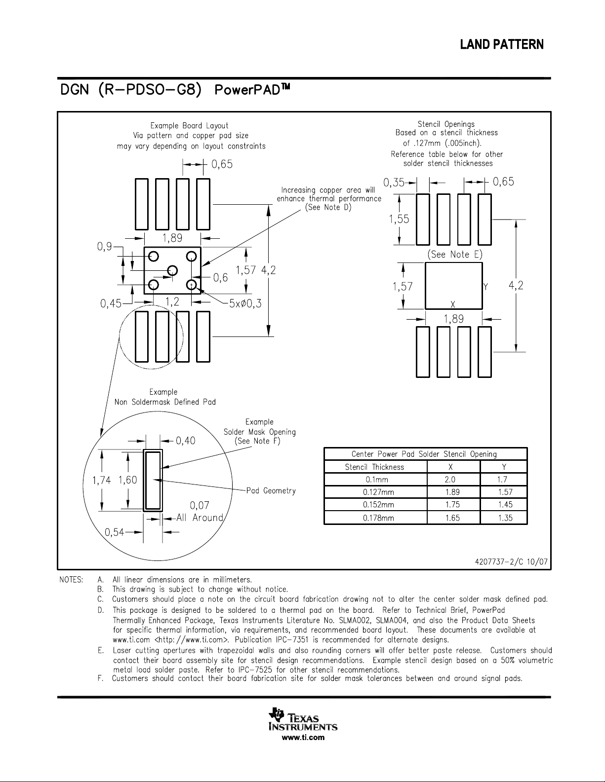
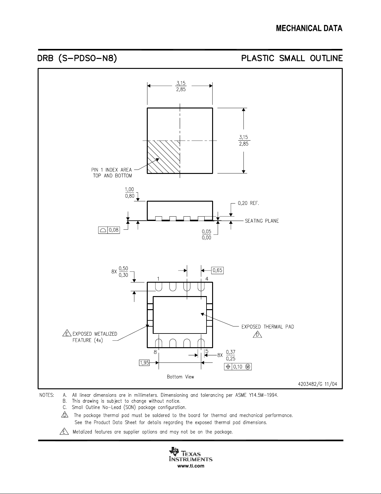
DRB
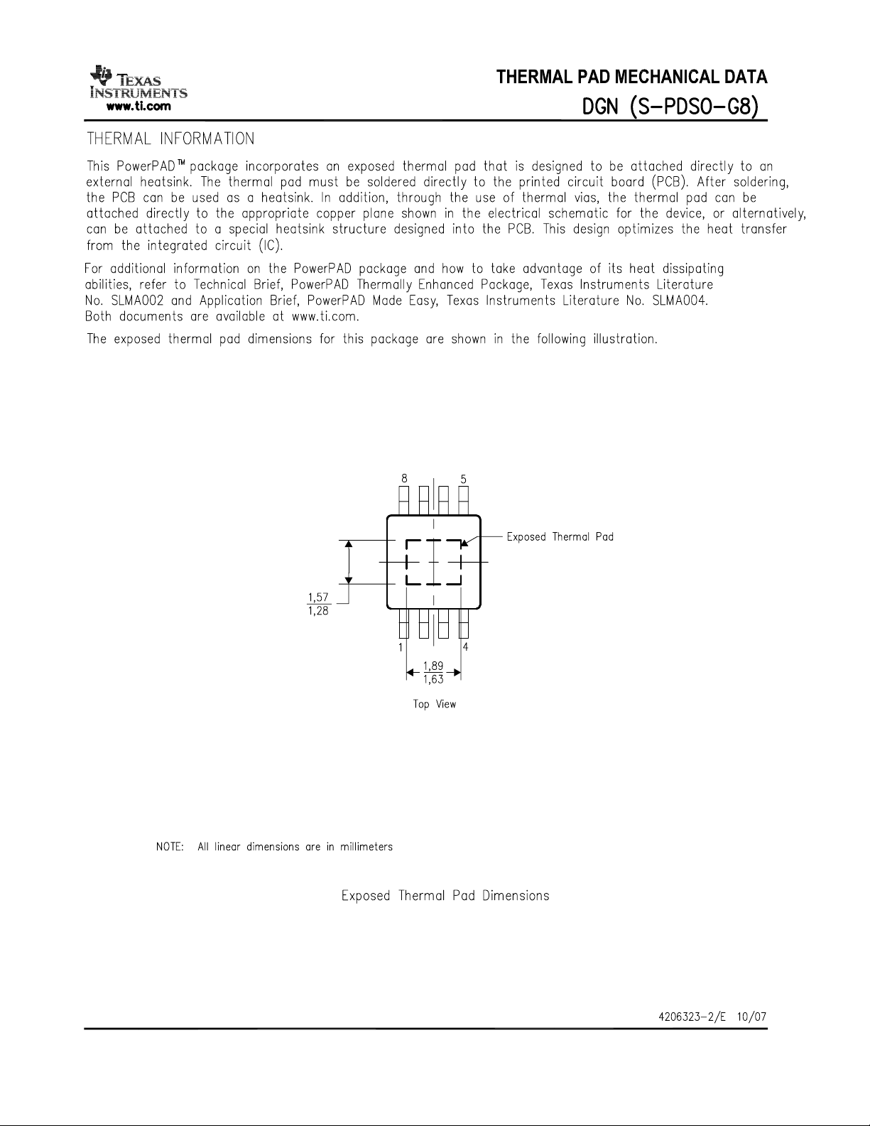
DGN
www.ti.com
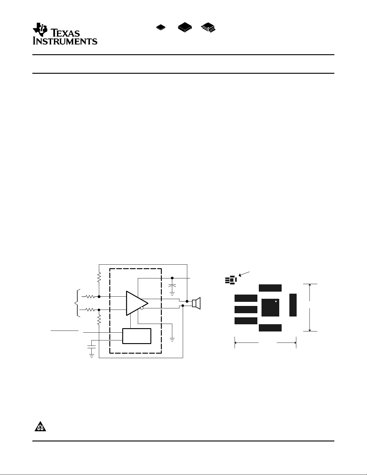
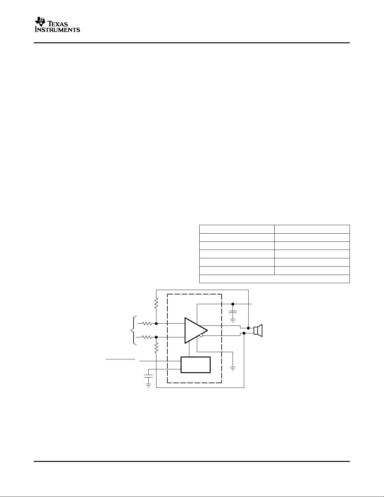
APPLICATION CIRCUIT
Actual Solution Siz e
6,9 mm
5,25 mm
(1)
C
B
R
I
R
I
C
S
R
F
R
F
_
+
V
DD
V
O+
V
O-
GND
To Battery
C
s
Bias
Circuitry
IN-
IN+
+
-
In From
DAC
SHUTDOWN
R
I
R
I
R
F
R
F
Applies to the GQV/ZQV Packages Only
C
( )
BYPASS
(Optional)
1.25-W MONO FULLY DIFFERENTIAL AUDIO POWER AMPLIFIER
FEATURES APPLICATIONS
• 1.25 W Into 8 Ω From a 5-V Supply at
THD = 1% (Typical)
• Low Supply Current: 1.7 mA Typical
• Shutdown Control < 10 µ A
• Only Five External Components
– Improved PSRR (90 dB) and Wide Supply
Voltage (2.5 V to 5.5 V) for Direct Battery
Operation
– Fully Differential Design Reduces RF
Rectification
– Improved CMRR Eliminates Two Input
Coupling Capacitors
– C
(BYPASS)
Design and High PSRR
• Avaliable in a 2 mm x 2 mm MicroStar
Junior ™ BGA Package (GQV, ZQV)
• Available in 3 mm x 3 mm QFN Package
(DRB)
• Available in an 8-Pin PowerPAD™ MSOP
(DGN)
Is Optional Due to Fully Differential
TPA6203A1
SLOS364E – MARCH 2002 – REVISED DECEMBER 2005
• Designed for Wireless or Cellular Handsets
and PDAs
DESCRIPTION
The TPA6203A1 is a 1.25-W mono fully differential
amplifier designed to drive a speaker with at least
8- Ω impedance while consuming less than 37 mm
(ZQV package option) total printed-circuit board
(PCB) area in most applications. This device operates
from 2.5 V to 5.5 V, drawing only 1.7 mA of quiescent
supply current. The TPA6203A1 is available in the
space-saving 2 mm x 2 mm MicroStar Junior™ BGA
package, and the space saving 3 mm x 3 mm QFN
(DRB) package.
Features like 85-dB PSRR from 90 Hz to 5 kHz,
improved RF-rectification immunity, and small PCB
area makes the TPA6203A1 ideal for wireless
handsets. A fast start-up time of 4 µ s with minimal
pop makes the TPA6203A1 ideal for PDA
applications.
2
Junior, PowerPAD, MicroStar Junior are trademarks of Texas Instruments.
PRODUCTION DATA information is current as of publication date.
Products conform to specifications per the terms of the Texas
Instruments standard warranty. Production processing does not
necessarily include testing of all parameters.
Please be aware that an important notice concerning availability, standard warranty, and use in critical applications of Texas Instruments semiconductor products and disclaimers thereto appears at the end of this data sheet.
Copyright © 2002–2005, Texas Instruments Incorporated
www.ti.com
TPA6203A1
SLOS364E – MARCH 2002 – REVISED DECEMBER 2005
These devices have limited built-in ESD protection. The leads should be shorted together or the device placed in conductive foam
during storage or handling to prevent electrostatic damage to the MOS gates.
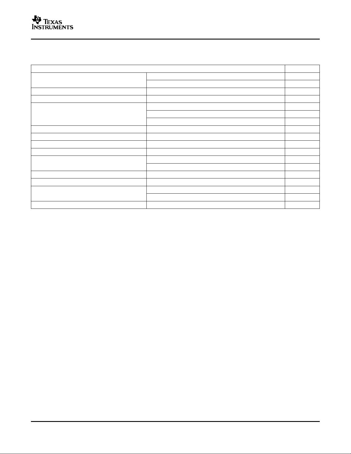
ORDERING INFORMATION
PACKAGED DEVICES
MicroStar Junior™ MicroStar Junior™ QFN MSOP
(GQV) (ZQV) (DRB) (DGN)
Device TPA6203A1GQVR TPA6203A1ZQVR TPA6203A1DRB TPA6203A1DGN
Symbolization AADI AAEI AAJI AAII
(1) The GQV is the standard MicroStar Junior package. The ZQV is a lead-free option and is qualified for 260 ° lead-free assembly.
(2) The GQV and ZQV packages are only available taped and reeled. The suffix R designates taped and reeled parts.
(3) For the most current package and ordering information, see the Package Option Addendum at the end of this document, or see the TI
website at www.ti.com .
ABSOLUTE MAXIMUM RATINGS
over operating free-air temperature range unless otherwise noted
Supply voltage, V
Input voltage, V
Continuous total power dissipation See Dissipation Rating Table
Operating free-air temperature, T
Junction temperature, T
Storage temperature, T
Lead temperature 1,6 mm (1/16 Inch) from case for 10 seconds
(1) Stresses beyond those listed under "absolute maximum ratings” may cause permanent damage to the device. These are stress ratings
only, and functional operation of the device at these or any other conditions beyond those indicated under "recommended operating
conditions” is not implied. Exposure to absolute-maximum-rated conditions for extended periods may affect device reliability.
DD
I
J
stg
INx and SHUTDOWN pins -0.3 V to V
A
(1)
ZQV, DRB, DGN 260 ° C
GQV 235 ° C
(1) (2) (3)
UNIT
-0.3 V to 6 V
DD
-40 ° C to 85 ° C
-40 ° C to 125 ° C
-65 ° C to 85 ° C
+ 0.3 V
RECOMMENDED OPERATING CONDITIONS
Supply voltage, V
High-level input voltage, V
Low-level input voltage, V
Common-mode input voltage, V
Operating free-air temperature, T
Load impedance, Z
DD
IH
IL
L
DISSIPATION RATINGS
PACKAGE DERATING FACTOR
GQV, ZQV 885 mW 8.8 mW/ ° C 486 mW 354 mW
DRB 2.7 W 21.8 mW/ ° C 1.7 W 1.4 W
2
MIN TYP MAX UNIT
2.5 5.5 V
SHUTDOWN 2 V
SHUTDOWN 0.8 V
V
IC
A
= 2.5 V, 5.5 V, CMRR ≤ -60 dB 0.5 VDD-0.8 V
DD
-40 85 ° C
6.4 8 Ω
TA≤ 25 ° C TA= 70 ° C TA= 85 ° C
POWER RATING POWER RATING POWER RATING
www.ti.com
TPA6203A1
SLOS364E – MARCH 2002 – REVISED DECEMBER 2005
ELECTRICAL CHARACTERISTICS
TA= 25 ° C, Gain = 1 V/V
PARAMETER TEST CONDITIONS MIN TYP MAX UNIT
|V
PSRR Power supply rejection ratio V
CMRR Common-mode rejection ratio dB
V
V
|IIH| High-level input current V
|IIL| Low-level input current V
I
DD
I
DD(SD)
Output offset voltage (measured
| VI= 0 V, V
OO
differentially)
= 2.5 V to 5.5 V -90 -70 dB
DD
V
= 3.6 V to 5.5 V, VIC= 0.5 V to VDD-0.8 -70 -65
DD
V
= 2.5 V, VIC= 0.5 V to 1.7 V -62 -55
DD
Low-level output voltage V
OL
High-level output voltage V
OH
Supply current V
RL= 8 Ω , V
V
= 0 V or V
IN-
RL= 8 Ω , V
V
= 0 V or V
IN-
= 5.5 V, VI= 5.8 V 1.2 µ A
DD
= 5.5 V, VI= -0.3 V 1.2 µ A
DD
= 2.5 V to 5.5 V, No load, SHUTDOWN = 2 V 1.7 2 mA
DD
= 2.5 V to 5.5 V 9 mV
DD
= VDD,
IN+
= 0 V, V
IN+
= VDD,
IN+
= 0 V, V
IN+
Supply current in shutdown mode SHUTDOWN = 0.8 V, V
V
= 5.5 V 0.30 0.46
DD
= 3.6 V 0.22 V
= V
IN-
DD
= V
IN-
DD
= 2.5 V to 5.5 V, No load 0.01 0.9 µ A
DD
DD
V
= 2.5 V 0.19 0.26
DD
V
= 5.5 V 4.8 5.12
DD
= 3.6 V 3.28 V
DD
V
= 2.5 V 2.1 2.24
DD
OPERATING CHARACTERISTICS
TA= 25 ° C, Gain = 1 V/V, RL= 8 Ω
PARAMETER TEST CONDITIONS MIN TYP MAX UNIT
V
= 5 V 1.25
DD
P
THD+N V
k
SVR
SNR Signal-to-noise ratio V
V
CMRR resistor tolerance = 0.1%, dB
Z
I
Z
O
Output power THD + N = 1%, f = 1 kHz V
O
V
= 5 V, PO= 1 W, f = 1 kHz 0.06%
Total harmonic distortion
plus noise
Supply ripple rejection ratio V
Output voltage noise f = 20 Hz to 20 kHz µ V
n
Common-mode rejection
ratio
DD
= 3.6 V, PO= 0.5 W, f = 1 kHz 0.07%
DD
V
= 2.5 V, PO= 200 mW, f = 1 kHz 0.08%
DD
C
(BYPASS)
V
DD
Inputs ac-grounded with CI= 2 µ F
C
(BYPASS)
DD
Inputs ac-grounded with CI= 2 µ F
C
(BYPASS)
V
DD
Inputs ac-grounded with CI= 2 µ F
DD
V
DD
gain = 4V/V, V
= 0.47 ° F,
= 3.6 V to 5.5 V, -87
= 0.47 µ F,
= 2.5 V to 3.6 V, -82 dB
= 0.47 µ F,
= 2.5 V to 5.5 V, ≤ -74
= 5 V, PO= 1 W 104 dB
= 2.5 V to 5.5 V, f = 20 Hz to 1 kHz ≤ -85
= 200 mV
ICM
PP
= 3.6 V 0.63 W
DD
V
= 2.5 V 0.3
DD
f = 217 Hz to 2 kHz,
V
= 200 mV
RIPPLE
PP
f = 217 Hz to 2 kHz,
V
= 200 mV
RIPPLE
PP
f = 40 Hz to 20 kHz,
V
= 200 mV
RIPPLE
PP
No weighting 17
A weighting 13
f = 20 Hz to 20 kHz ≤ -74
Input impedance 2 M Ω
Output impedance Shutdown mode >10k
Shutdown attenuation f = 20 Hz to 20 kHz, RF= RI= 20 k Ω -80 dB
RMS
3
www.ti.com
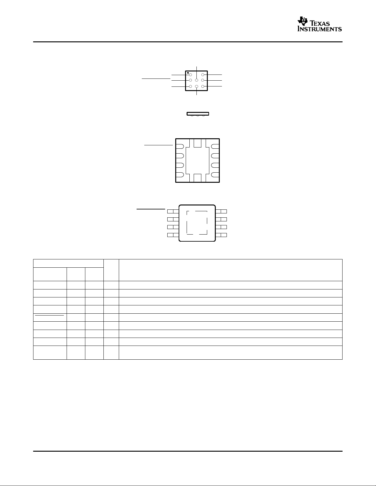
(SIDE VIEW)
SHUTDOWN
IN+
V
DD
V
O+
GND
V
O-
IN-
A
B
C
1 2 3
BYPASS
8
SHUTDOWN
BYPASS
IN+
IN-
V
O-
GND
V
DD
V
O+
7
6
5
1
2
3
4
7
6
5
1
2
3
SHUTDOWN
BYPASS
IN+
IN-
V
O-
GND
V
DD
V
O+
4
8
TPA6203A1
SLOS364E – MARCH 2002 – REVISED DECEMBER 2005
MicroStar Junior™ (GQV or ZQV) PACKAGE
(TOP VIEW)
8-PIN QFN (DRB) PACKAGE
(TOP VIEW)
8-PIN MSOP (DGN) PACKAGE
(TOP VIEW)
Terminal Functions
TERMINAL
NAME GQV
DRB,
DGN
BYPASS C1 2 I Mid-supply voltage. Adding a bypass capacitor improves PSRR.
GND B2 7 I High-current ground
IN- C3 4 I Negative differential input
IN+ C2 3 I Positive differential input
SHUTDOWN B1 1 I Shutdown terminal (active low logic)
V
DD
V
O+
V
O-
A3 6 I Supply voltage terminal
B3 5 O Positive BTL output
A1 8 O Negative BTL output
Thermal Pad
I/O DESCRIPTION
Connect to ground. Thermal pad must be soldered down in all applications to properly secure device
on the PCB.
4
www.ti.com
Table of Graphs
P
P
CMRR Common-mode rejection ratio
I
DD
Output power
O
Power dissipation vs Output power 4, 5
D
Maximum ambient temperature vs Power dissipation 6
Total harmonic distortion + noise vs Frequency 9, 10, 11, 12
Supply voltage rejection ratio vs Frequency 14, 15, 16, 17
Supply voltage rejection ratio vs Common-mode input voltage 18
GSM Power supply rejection vs Time 19
GSM Power supply rejection vs Frequency 20
Closed loop gain/phase vs Frequency 23
Open loop gain/phase vs Frequency 24
Supply current
Start-up time vs Bypass capacitor 27
TPA6203A1
SLOS364E – MARCH 2002 – REVISED DECEMBER 2005
TYPICAL CHARACTERISTICS
FIGURE
vs Supply voltage 1
vs Load resistance 2, 3
vs Output power 7, 8
vs Common-mode input voltage 13
vs Frequency 21
vs Common-mode input voltage 22
vs Supply voltage 25
vs Shutdown voltage 26
5
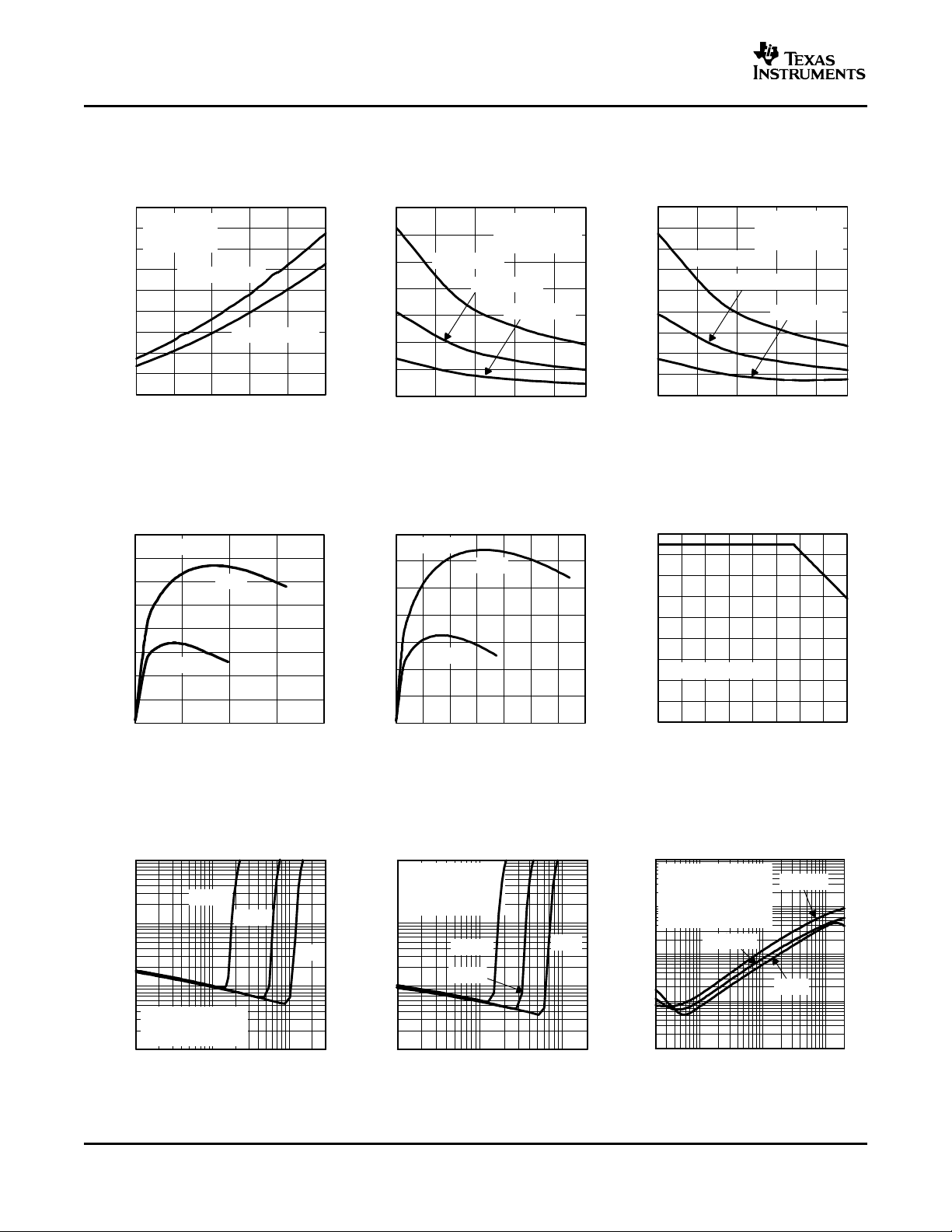
www.ti.com
0
0.2
0.4
0.6
0.8
1
1.2
1.4
1.6
1.8
8 13 18 23 28
VDD = 5 V
VDD = 3.6 V
VDD = 2.5 V
R
L
- Load Resistance - Ω
- Output Power - WP
O
f = 1 kHz
THD+N = 10%
Gain = 1 V/V
32
0
0.2
0.4
0.6
0.8
1
1.2
1.4
1.6
1.8
2.5 3 3.5 4 4.5 5
V
DD
- Supply Voltage - V
- Output Power - WP
O
RL = 8 Ω
f = 1 kHz
Gain = 1 V/V
THD+N = 1%
THD+N = 10%
0
0.2
0.4
0.6
0.8
1
1.2
1.4
8 13 18 23 28
VDD = 5 V
VDD = 3.6 V
VDD = 2.5 V
R
L
- Load Resistance - Ω
- Output Power - WP
O
f = 1 kHz
THD+N = 1%
Gain = 1 V/V
32
0
10
20
30
40
50
60
70
80
90
0 0.1 0.2 0.3 0.4 0.5 0.6 0.7 0.8
PD- Power Dissipation - W
Maximum Ambient Temperature - C
o
ZQV Package Only
0
0.05
0.1
0.15
0.2
0.25
0.3
0.35
0.4
0 0.2 0.4 0.6 0.8
8 Ω
16 Ω
P
O
- Output Power - W
- Power Dissipation - WP
D
VDD = 3.6 V
0 0.2 0.4 0.6 0.8 1 1.2 1.4
8 Ω
16 Ω
P
O
- Output Power - W
- Power Dissipation - WP
D
VDD = 5 V
0
0.1
0.2
0.3
0.4
0.5
0.6
0.7
VDD = 5 V
CI = 2 µF
RL = 8 Ω
C
(Bypass)
= 0 to 1 µF
Gain = 1 V/V
0.001
10
0.002
0.005
0.01
0.02
0.05
0.1
0.2
0.5
1
2
5
20 20 k100 200 1 k 2 k 10 k
f - Frequency - Hz
THD+N - Total Harmonic Distortion + Noise - %
50 mW
250 mW
1 W
10
0.01
0.02
0.05
0.1
0.2
0.5
1
2
5
10 m 3100 m 1 2
PO - Output Power - W
THD+N - Total Harmonic Distortion + Noise - %
2.5 V
3.6 V
5 V
RL = 8 Ω, f = 1 kHz
C
(Bypass)
= 0 to 1 µF
Gain = 1 V/V
10
0.01
0.02
0.05
0.1
0.2
0.5
1
2
5
10 m 100 m 1 2
PO - Output Power - W
THD+N - Total Harmonic Distortion + Noise - %
2.5 V
5 V
3.6 V
RL = 16 Ω
f = 1 kHz
C
(Bypass)
= 0 to 1 µF
Gain = 1 V/V
TPA6203A1
SLOS364E – MARCH 2002 – REVISED DECEMBER 2005
OUTPUT POWER OUTPUT POWER OUTPUT POWER
vs vs vs
SUPPLY VOLTAGE LOAD RESISTANCE LOAD RESISTANCE
Figure 1. Figure 2. Figure 3.
TYPICAL CHARACTERISTICS
POWER DISSIPATION POWER DISSIPATION MAXIMUM AMBIENT
vs vs TEMPERATURE
OUTPUT POWER OUTPUT POWER vs
POWER DISSIPATION
Figure 4. Figure 5. Figure 6.
TOTAL HARMONIC DISTORTION + TOTAL HARMONIC DISTORTION + TOTAL HARMONIC DISTORTION +
NOISE NOISE NOISE
vs vs vs
OUTPUT POWER OUTPUT POWER FREQUENCY
6
Figure 7. Figure 8. Figure 9.
www.ti.com
0.001
10
0.002
0.005
0.01
0.02
0.05
0.1
0.2
0.5
1
2
5
20 20 k50 100 200 500 1 k 2 k 5 k 10 k
f - Frequency - Hz
THD+N - Total Harmonic Distortion + Noise - %
25 mW
125 mW
500 mW
VDD = 3.6 V
CI = 2 µF
RL = 8 Ω
C
(Bypass)
= 0 to 1 µF
Gain = 1 V/V
0.001
10
0.002
0.005
0.01
0.02
0.05
0.1
0.2
0.5
1
2
5
20 20 k50 100 200 500 1 k 2 k 5 k 10 k
f - Frequency - Hz
THD+N - Total Harmonic Distortion + Noise - %
15 mW
200 mW
75 mW
VDD = 2.5 V
CI = 2 µF
RL = 8 Ω
C
(Bypass)
= 0 to 1 µF
Gain = 1 V/V
VDD = 3.6 V
CI = 2 µF
RL = 16 Ω
C
(Bypass)
= 0 to 1 µF
Gain = 1 V/V
0.001
10
0.002
0.005
0.01
0.02
0.05
0.1
0.2
0.5
1
2
5
20 20 k50 100 200 500 1 k 2 k 5 k 10 k
f - Frequency - Hz
THD+N - Total Harmonic Distortion + Noise - %
25 mW
250 mW
125 mW
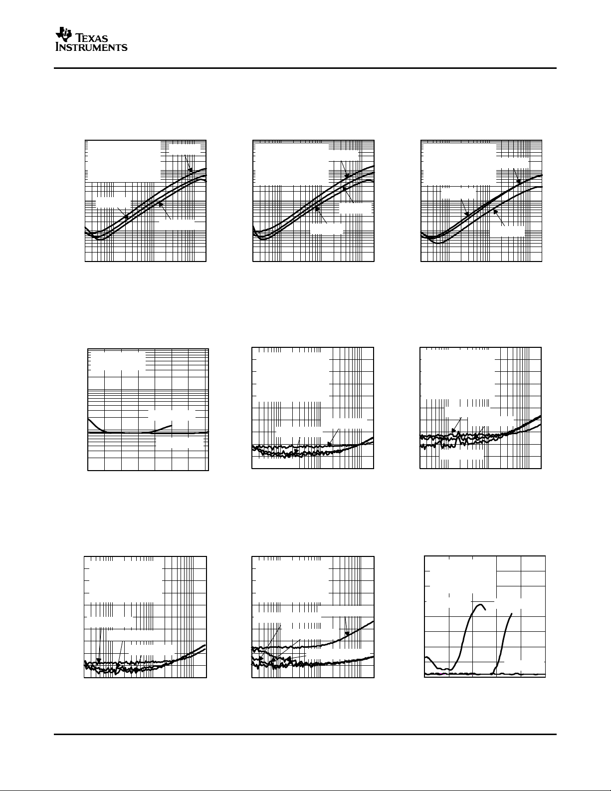
-100
0
-90
-80
-70
-60
-50
-40
-30
-20
-10
20 20 k50 100 200 500 1 k 2 k 5 k 10 k
VDD = 3.6 V
VDD = 5 V
VDD =2. 5 V
f - Frequency - Hz
- Supply Voltage Rejection Ratio - dBk
SVR
CI = 2 µF
RL = 8 Ω
C
(Bypass)
= 0.47 µF
V
p-p
= 200 mV
Inputs ac-Grounded
Gain = 1 V/V
-100
0
-90
-80
-70
-60
-50
-40
-30
-20
-10
20 20 k50 100 200 500 1 k 2 k 5 k 10 k
f - Frequency - Hz
- Supply Voltage Rejection Ratio - dBk
SVR
VDD = 3.6 V
VDD = 5 V
VDD =2. 5 V
Gain = 5 V/V
CI = 2 µF
RL = 8 Ω
C
(Bypass)
= 0.47 µF
V
p-p
= 200 mV
Inputs ac-Grounded
0.01
0.10
1
10
0 0.5 1 1.5 2 2.5 3 3.5
VDD = 2.5 V
VDD = 3.6 V
f = 1 kHz
PO = 200 mW
V
IC
- Common Mode Input Voltage - V
THD+N - Total Harmonic Distortion + Noise - %
-90
-80
-70
-60
-50
-40
-30
-20
-10
0 1 2 3 4 5
V
IC
- Common Mode Input Voltage - V
f = 217 Hz
C
(Bypass)
= 0.47 µF
RL = 8 Ω
Gain = 1 V/V
VDD = 2.5 V
VDD = 3.6 V
VDD = 5 V
- Supply Voltage Rejection Ratio - dBk
SVR
-100
0
-90
-80
-70
-60
-50
-40
-30
-20
-10
20 20 k50 100 200 500 1 k 2 k 5 k 10 k
f - Frequency - Hz
- Supply Voltage Rejection Ratio - dBk
SVR
VDD =2. 5 V
VDD = 5 V
VDD = 3.6 V
CI = 2 µF
RL = 8 Ω
Inputs Floating
Gain = 1 V/V
VDD = 3.6 V
CI = 2 µF
RL = 8 Ω
Inputs ac-Grounded
Gain = 1 V/V
-100
0
-90
-80
-70
-60
-50
-40
-30
-20
-10
20 20 k50 100 200 500 1 k 2 k 5 k 10 k
f - Frequency - Hz
- Supply Voltage Rejection Ratio - dBk
SVR
C
(Bypass)
= 0.1 µF
C
(Bypass)
= 0
C
(Bypass)
= 0.47 µF
C
(Bypass)
= 1 µF
TYPICAL CHARACTERISTICS (continued)
TPA6203A1
SLOS364E – MARCH 2002 – REVISED DECEMBER 2005
TOTAL HARMONIC DISTORTION + TOTAL HARMONIC DISTORTION + TOTAL HARMONIC DISTORTION +
NOISE NOISE NOISE
vs vs vs
FREQUENCY FREQUENCY FREQUENCY
Figure 10. Figure 11. Figure 12.
TOTAL HARMONIC DISTORTION + SUPPLY VOLTAGE REJECTION SUPPLY VOLTAGE REJECTION
NOISE RATIO RATIO
vs vs vs
COMMON MODE INPUT VOLTAGE FREQUENCY FREQUENCY
SUPPLY VOLTAGE REJECTION SUPPLY VOLTAGE REJECTION SUPPLY VOLTAGE REJECTION
Figure 13. Figure 14. Figure 15.
RATIO RATIO RATIO
vs vs vs
FREQUENCY FREQUENCY COMMON MODE INPUT VOLTAGE
Figure 16. Figure 17. Figure 18.
7
www.ti.com
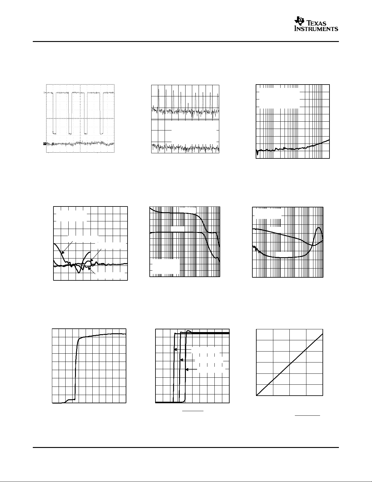
f - Frequency - Hz
0
-50
-100
0 200 400 600 800 1k 1.2k
- Output Voltage - dBV
1.4k1.6k 1.8k 2k
-150
-150
-100
0
-50
V
O
- Supply Voltage - dBVV
DD
VDD Shown in Figure 19
CI = 2 µF,
C
(Bypass)
= 0.47 µF,
Inputs ac-Grounded
Gain = 1V/V
C1
Frequency
217.41 Hz
C1 - Duty
20 %
C1 High
3.598 V
C1 Pk-Pk
504 mV
Voltage - V
Ch1 100 mV/div
Ch4 10 mV/div
2 ms/div
t - Time - ms
V
DD
V
O
-100
0
-90
-80
-70
-60
-50
-40
-30
-20
-10
20 20 k50 100 200 500 1 k 2 k 5 k 10 k
f - Frequency - Hz
CMRR - Common Mode Rejection Ratio - dB
VDD = 2.5 V to 5 V
VIC = 200 mV
p-p
RL = 8 Ω
Gain = 1 V/V
-70
-60
-50
-40
-30
-20
-10
0
10
20
30
40
10 100 10 k 100 k 1 M 10 M
-220
-180
-140
-100
-60
-20
20
60
100
140
180
220
1 k
f - Frequency - Hz
Gain - dB
Phase - Degrees
Gain
Phase
VDD = 3.6 V
RL = 8 Ω
Gain = 1 V/V
-200
-150
-100
-50
0
50
100
150
200
100 1 k 10 k 100 k 1 M
-200
-150
-100
-50
0
50
100
150
200
f - Frequency - Hz
Gain - dB
Phase - Degrees
Gain
Phase
VDD = 3.6 V
RL = 8 Ω
10 M
-100
-90
-80
-70
-60
-50
-40
-30
-20
-10
0
0 0.5 1 1.5 2 2.5 3 3.5 4 4.5 5
RL = 8 Ω
Gain = 1 V/V
V
IC
- Common Mode Input Voltage - V
CMRR - Common Mode Rejection Ratio - dB
VDD = 3.6 V
VDD = 5 V
VDD = 2.5 V
0
0.2
0.4
0.6
0.8
1
1.2
1.4
1.6
1.8
0 0.5 1 1.5 2 2.5 3 3.5 4 4.5 5 5.5
V
DD
- Supply Voltage - V
- Supply Current - mA
I
DD
0
0.4
0.6
0.8
1.0
1.2
1.4
1.6
1.8
1
1.1 1.2 1.3 1.4 1.5 1.6 1.7 1.8 1.9
2
VDD = 2.5 V
VDD = 3.6 V
VDD = 5 V
Voltage on SHUTDOWN Terminal - V
- Supply Current - mA
I
DD
0.2
0
1
2
3
4
5
6
0 0.5 1 1.5 2
C
(Bypass)
- Bypass Capacitor - µF
Start-Up Time - ms
(1)
Start-Up time is the time it takes (from a
low-to-high transition on SHUTDOWN) for the
gain of the amplifier to reach -3 dB of the final
gain.
TPA6203A1
SLOS364E – MARCH 2002 – REVISED DECEMBER 2005
GSM POWER SUPPLY GSM POWER SUPPLY COMMON MODE REJECTION RATIO
REJECTION REJECTION vs
vs vs FREQUENCY
TIME FREQUENCY
Figure 19. Figure 20. Figure 21.
TYPICAL CHARACTERISTICS (continued)
COMMON MODE REJECTION RATIO CLOSED LOOP GAIN/PHASE OPEN LOOP GAIN/PHASE
vs vs vs
COMMON MODE INPUT VOLTAGE FREQUENCY FREQUENCY
Figure 22. Figure 23. Figure 24.
SUPPLY CURRENT SUPPLY CURRENT
vs vs
SUPPLY VOLTAGE SHUTDOWN VOLTAGE
START-UP TIME
BYPASS CAPACITOR
(1)
vs
8
Figure 25. Figure 26. Figure 27.
www.ti.com
APPLICATION INFORMATION
_
+
V
DD
V
O+
V
O-
GND
To Battery
C
s
Bias
Circuitry
IN-
IN+
+
-
In From
DAC
SHUTDOWN
R
I
R
I
C
( )
BYPASS
(Optional)
R
F
R
F
FULLY DIFFERENTIAL AMPLIFIER
The TPA6203A1 is a fully differential amplifier with
differential inputs and outputs. The fully differential
amplifier consists of a differential amplifier and a
common- mode amplifier. The differential amplifier
ensures that the amplifier outputs a differential
voltage that is equal to the differential input times the
gain. The common-mode feedback ensures that the
common-mode voltage at the output is biased around
V
/2 regardless of the common- mode voltage at the
DD
input.
Advantages of Fully Differential Amplifiers
• Input coupling capacitors not required: A fully
differential amplifier with good CMRR, like the
TPA6203A1, allows the inputs to be biased at
voltage other than mid-supply. For example, if a
DAC has mid-supply lower than the mid-supply of
the TPA6203A1, the common-mode feedback
circuit adjusts for that, and the TPA6203A1
outputs are still biased at mid-supply of the
TPA6203A1. The inputs of the TPA6203A1 can
be biased from 0.5 V to V
are biased outside of that range, input coupling
capacitors are required.
- 0.8 V. If the inputs
DD
SLOS364E – MARCH 2002 – REVISED DECEMBER 2005
• Mid-supply bypass capacitor, C
(BYPASS)
required: The fully differential amplifier does not
require a bypass capacitor. This is because any
shift in the mid-supply affects both positive and
negative channels equally and cancels at the
differential output. However, removing the bypass
capacitor slightly worsens power supply rejection
ratio (k
), but a slight decrease of k
SVR
acceptable when an additional component can be
eliminated (see Figure 17 ).
• Better RF-immunity: GSM handsets save power
by turning on and shutting off the RF transmitter
at a rate of 217 Hz. The transmitted signal is
picked-up on input and output traces. The fully
differential amplifier cancels the signal much
better than the typical audio amplifier.
APPLICATION SCHEMATICS
Figure 28 through Figure 30 show application
schematics for differential and single-ended inputs.
Typical values are shown in Table 1 .
Table 1. Typical Component Values
COMPONENT VALUE
R
I
R
F
C
C
C
(1) C
(1)
(BYPASS)
S
I
(BYPASS)
is optional
10 k Ω
10 k Ω
0.22 µ F
1 µ F
0.22 µ F
TPA6203A1
, not
may be
SVR
Figure 28. Typical Differential Input Application Schematic
9

www.ti.com
_
+
V
DD
V
O+
V
O-
GND
To Battery
C
s
Bias
Circuitry
IN-
IN+
+
-
IN
SHUTDOWN
R
I
R
I
R
F
R
F
C
I
C
I
C
( )
BYPASS
(Optional)
_
+
V
DD
V
O+
V
O-
GND
To Battery
C
s
Bias
Circuitry
IN-
IN+
IN
SHUTDOWN
R
I
R
F
C
I
C
I
R
I
R
F
C
( )
BYPASS
(Optional)
Gain = RF/R
I
TPA6203A1
SLOS364E – MARCH 2002 – REVISED DECEMBER 2005
Figure 29. Differential Input Application Schematic Optimized With Input Capacitors
Figure 30. Single-Ended Input Application Schematic
Selecting Components
Resistors (R
The input (R
gain of the amplifier according to Equation 1 .
R
and R
F
graphs were taken with R
Resistor matching is very important in fully differential
amplifiers. The balance of the output on the reference
voltage depends on matched ratios of the resistors.
CMRR, PSRR, and the cancellation of the second
harmonic distortion diminishes if resistor mismatch
occurs. Therefore, it is recommended to use 1%
tolerance resistors or better to keep the performance
optimized.
10
and RI)
F
) and feedback resistors (R
I
should range from 1 k Ω to 100 k Ω . Most
I
= RI= 20 k Ω .
F
F
) set the
Bypass Capacitor (C
BYPASS
) and Start-Up Time
The internal voltage divider at the BYPASS pin of this
device sets a mid-supply voltage for internal
references and sets the output common mode
voltage to V
any noise into this pin and increases the k
(1)
C
(BYPASS)
/2. Adding a capacitor to this pin filters
DD
also determines the rise time of V
.
SVR
and V
O+
O-
when the device is taken out of shutdown. The larger
the capacitor, the slower the rise time. Although the
output rise time depends on the bypass capacitor
value, the device passes audio 4 µ s after taken out of
shutdown and the gain is slowly ramped up based on
C
(BYPASS)
.
To minimize pops and clicks, design the circuit so the
impedance (resistance and capacitance) detected by
both inputs, IN+ and IN-, is equal.

www.ti.com
f
c
1
2RIC
I
–3 dB
f
c
C
I
1
2RIf
c
TPA6203A1
SLOS364E – MARCH 2002 – REVISED DECEMBER 2005
Input Capacitor (C
) Decoupling Capacitor (C
I
)
S
The TPA6203A1 does not require input coupling The TPA6203A1 is a high-performance CMOS audio
capacitors if using a differential input source that is amplifier that requires adequate power supply
biased from 0.5 V to V
- 0.8 V. Use 1% tolerance decoupling to ensure the output total harmonic
DD
or better gain-setting resistors if not using input distortion (THD) is as low as possible. Power supply
coupling capacitors. decoupling also prevents oscillations for long lead
In the single-ended input application an input
capacitor, CI, is required to allow the amplifier to bias
the input signal to the proper dc level. In this case, C
and R
form a high-pass filter with the corner
I
frequency determined in Equation 2 .
lengths between the amplifier and the speaker. For
higher frequency transients, spikes, or digital hash on
the line, a good low equivalent-series- resistance
I
(ESR) ceramic capacitor, typically 0.1 µ F to 1 µ F,
placed as close as possible to the device V
works best. For filtering lower frequency noise
signals, a 10- µ F or greater capacitor placed near the
(2)
audio power amplifier also helps, but is not required
in most applications because of the high PSRR of this
device.
USING LOW-ESR CAPACITORS
Low-ESR capacitors are recommended throughout
this applications section. A real (as opposed to ideal)
capacitor can be modeled simply as a resistor in
series with an ideal capacitor. The voltage drop
across this resistor minimizes the beneficial effects of
the capacitor in the circuit. The lower the equivalent
value of this resistance the more the real capacitor
behaves like an ideal capacitor.
lead
DD
The value of CIis important to consider as it directly
affects the bass (low frequency) performance of the
circuit. Consider the example where RIis 10 k Ω and
the specification calls for a flat bass response down
to 100 Hz. Equation 2 is reconfigured as Equation 3 .
In this example, C
is 0.16 µ F, so one would likely
I
choose a value in the range of 0.22 µ F to 0.47 µ F. A
further consideration for this capacitor is the leakage
path from the input source through the input network
(R
, CI) and the feedback resistor (R
I
) to the load.
F
This leakage current creates a dc offset voltage at the
input to the amplifier that reduces useful headroom,
especially in high gain applications. For this reason, a
ceramic capacitor is the best choice. When polarized
capacitors are used, the positive side of the capacitor
should face the amplifier input in most applications,
as the dc level there is held at V
/2, which is likely
DD
higher than the source dc level. It is important to
confirm the capacitor polarity in the application.
DIFFERENTIAL OUTPUT VERSUS SINGLE-ENDED OUTPUT
Figure 31 shows a Class-AB audio power amplifier
(APA) in a fully differential configuration. The
TPA6203A1 amplifier has differential outputs driving
(3)
both ends of the load. There are several potential
benefits to this differential drive configuration, but
initially consider power to the load. The differential
drive to the speaker means that as one side is
slewing up, the other side is slewing down, and vice
versa. This in effect doubles the voltage swing on the
load as compared to a ground referenced load.
Plugging 2 × V
into the power equation, where
O(PP)
voltage is squared, yields 4 × the output power from
the same supply rail and load impedance (see
Equation 4 ).
11

www.ti.com
V
(rms)
V
O(PP)
2 2
Power
V
(rms)
2
R
L
f
c
1
2RLC
C
R
L
2x V
O(PP)
V
O(PP)
–V
O(PP)
V
DD
V
DD
R
L
C
C
V
O(PP)
V
O(PP)
V
DD
–3 dB
f
c
TPA6203A1
SLOS364E – MARCH 2002 – REVISED DECEMBER 2005
low-frequency performance of the system. This
frequency-limiting effect is due to the high pass filter
network created with the speaker impedance and the
coupling capacitance and is calculated with
Equation 5 .
Figure 31. Differential Output Configuration
In a typical wireless handset operating at 3.6 V,
bridging raises the power into an 8- Ω speaker from a
singled-ended (SE, ground reference) limit of 200
mW to 800 mW. In sound power that is a 6-dB
improvement—which is loudness that can be heard.
In addition to increased power there are frequency
response concerns. Consider the single-supply SE
configuration shown in Figure 32 . A coupling
capacitor is required to block the dc offset voltage
from reaching the load. This capacitor can be quite
large (approximately 33 µ F to 1000 µ F) so it tends to
be expensive, heavy, occupy valuable PCB area, and
have the additional drawback of limiting
(4)
(5)
For example, a 68- µ F capacitor with an 8- Ω speaker
would attenuate low frequencies below 293 Hz. The
BTL configuration cancels the dc offsets, which
eliminates the need for the blocking capacitors.
Low-frequency performance is then limited only by
the input network and speaker response. Cost and
PCB space are also minimized by eliminating the
bulky coupling capacitor.
Figure 32. Single-Ended Output and Frequency
Response
Increasing power to the load does carry a penalty of
increased internal power dissipation. The increased
dissipation is understandable considering that the
BTL configuration produces 4 × the output power of
the SE configuration.
12

www.ti.com
FULLY DIFFERENTIAL AMPLIFIER
V
(LRMS)
V
O
I
DD
I
DD(avg)
Efficiency of a BTL amplifier
P
L
P
SUP
where:
P
L
VLrms
2
R
L
, andV
LRMS
V
P
2
, therefore, P
L
V
P
2
2R
L
PL = Power delivered to load
P
SUP
= Power drawn from power supply
V
LRMS
= RMS voltage on BTL load
RL = Load resistance
VP = Peak voltage on BTL load
IDDavg = Average current drawn from the
power supply
VDD = Power supply voltage
η
BTL
= Efficiency of a BTL amplifier
and
P
SUP
VDDIDDavg
and
IDDavg
1
0
V
P
R
L
sin(t) dt
1
V
P
R
L
[cos(t)]
0
2V
P
R
L
Therefore,
P
SUP
2 VDDV
P
R
L
substituting PL and P
SUP
into equation 6,
Efficiency of a BTL amplifier
V
P
2
2 R
L
2 VDDV
P
R
L
V
P
4 V
DD
VP 2 PLR
L
where:
EFFICIENCY AND THERMAL INFORMATION
Class-AB amplifiers are inefficient. The primary cause
of these inefficiencies is voltage drop across the
output stage transistors. There are two components
of the internal voltage drop. One is the headroom or
dc voltage drop that varies inversely to output power.
The second component is due to the sinewave nature
of the output. The total voltage drop can be
calculated by subtracting the RMS value of the output
voltage from V
by the average value of the supply current, IDD(avg),
determines the internal power dissipation of the
amplifier.
An easy-to-use equation to calculate efficiency starts
out as being equal to the ratio of power from the
power supply to the power delivered to the load. To
accurately calculate the RMS and average values of
power in the load and in the amplifier, the current and
voltage waveform shapes must first be understood
(see Figure 33 ).
. The internal voltage drop multiplied
DD
TPA6203A1
SLOS364E – MARCH 2002 – REVISED DECEMBER 2005
Figure 33. Voltage and Current Waveforms for
BTL Amplifiers
Although the voltages and currents for SE and BTL
are sinusoidal in the load, currents from the supply
are very different between SE and BTL
configurations. In an SE application the current
waveform is a half-wave rectified shape, whereas in
BTL it is a full-wave rectified waveform. This means
RMS conversion factors are different. Keep in mind
that for most of the waveform both the push and pull
transistors are not on at the same time, which
supports the fact that each amplifier in the BTL
device only draws current from the supply for half the
waveform. The following equations are the basis for
calculating amplifier efficiency.
(6)
13

www.ti.com
Θ
JA
1
Derating Factor
1
0.0088
113°CW
BTL
2 PLR
L
4 V
DD
Therefore,
TAMax TJMax ΘJAP
Dmax
125 113(0.634) 53.3°C
P
Dmax
2 V
2
DD
2
R
L
TPA6203A1
SLOS364E – MARCH 2002 – REVISED DECEMBER 2005
Table 2. Efficiency and Maximum Ambient
Temperature vs Output Power in 5-V 8- Ω BTL
Systems
Output Internal
Power Dissipation
(W) (W)
0.25 31.4 0.55 0.75 62
0.50 44.4 0.62 1.12 54
1.00 62.8 0.59 1.59 58
1.25 70.2 0.53 1.78 65
Efficiency From Ambient
(%) Supply Temperature
Table 2 employs Equation 7 to calculate efficiencies
for four different output power levels. Note that the
efficiency of the amplifier is quite low for lower power
levels and rises sharply as power to the load is
increased resulting in a nearly flat internal power
dissipation over the normal operating range. Note that
the internal dissipation at full output power is less
than in the half power range. Calculating the
efficiency for a specific system is the key to proper
power supply design. For a 1.25-W audio system with
8- Ω loads and a 5-V supply, the maximum draw on
the power supply is almost 1.8 W.
A final point to remember about Class-AB amplifiers
is how to manipulate the terms in the efficiency
equation to the utmost advantage when possible.
Note that in Equation 7 , V
This indicates that as V
goes down, efficiency goes
DD
up.
A simple formula for calculating the maximum power
dissipated, P
, may be used for a differential
Dmax
output application:
P
for a 5-V, 8- Ω system is 634 mW.
Dmax
The maximum ambient temperature depends on the
heat sinking ability of the PCB system. The derating
factor for the 2 mm x 2 mm Microstar Junior™
package is shown in the dissipation rating table.
Converting this to θJA:
Power Max
(W) ( ° C)
is in the denominator.
DD
(9)
Given θJA, the maximum allowable junction
(7)
temperature, and the maximum internal dissipation,
the maximum ambient temperature can be calculated
with the following equation. The maximum
recommended junction temperature for the
TPA6203A1 is 125 ° C.
(10)
Equation 10 shows that the maximum ambient
temperature is 53.3 ° C at maximum power dissipation
with a 5-V supply.
Table 2 shows that for most applications no airflow is
required to keep junction temperatures in the
specified range. The TPA6203A1 is designed with
thermal protection that turns the device off when the
junction temperature surpasses 150 ° C to prevent
damage to the IC. Also, using more resistive than 8- Ω
speakers dramatically increases the thermal
performance by reducing the output current.
PCB LAYOUT
In making the pad size for the BGA balls, it is
recommended that the layout use soldermask-defined (SMD) land. With this method, the
copper pad is made larger than the desired land area,
and the opening size is defined by the opening in the
solder mask material. The advantages normally
associated with this technique include more closely
controlled size and better copper adhesion to the
laminate. Increased copper also increases the
thermal performance of the IC. Better size control is
the result of photo imaging the stencils for masks.
Small plated vias should be placed near the center
ball connecting ball B2 to the ground plane. Added
plated vias and ground plane act as a heatsink and
increase the thermal performance of the device.
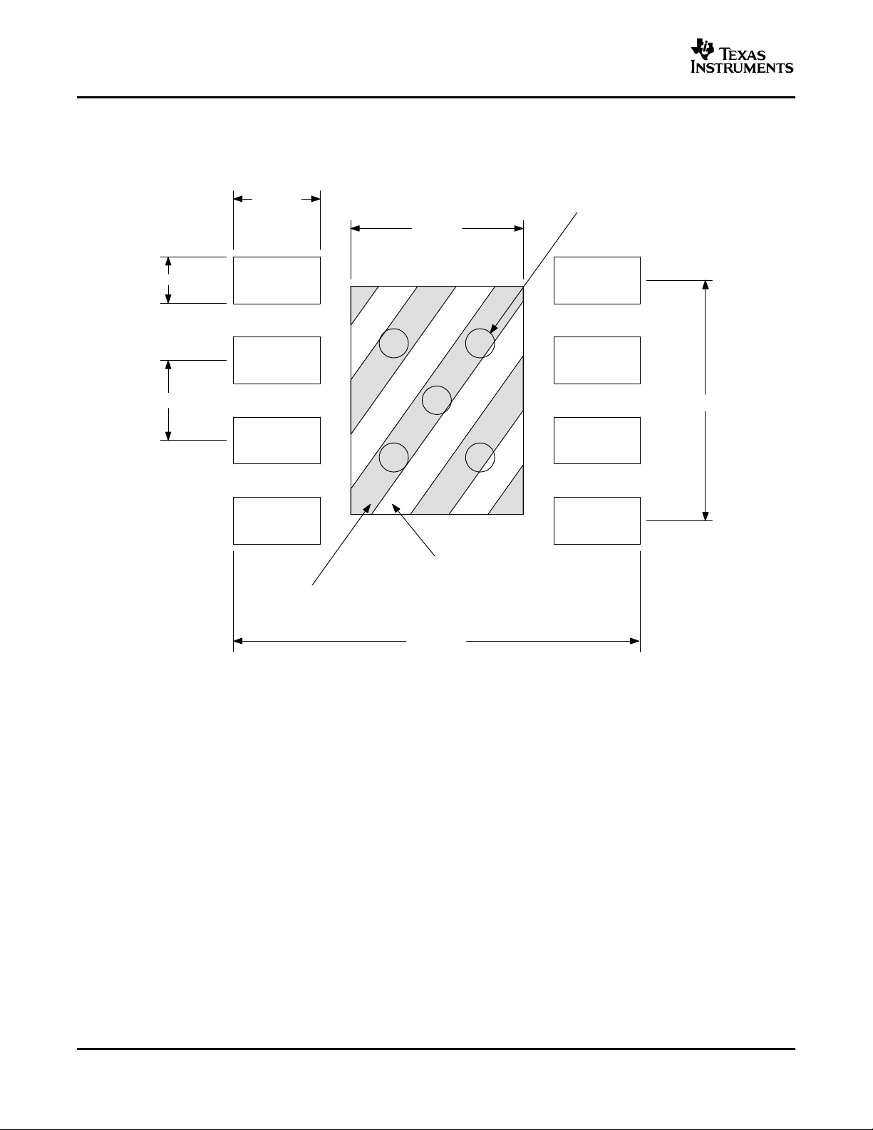
Figure 34 shows the appropriate diameters for a 2
(8)
mm X 2 mm MicroStar Junior™ BGA layout.
It is very important to keep the TPA6203A1 external
components very close to the TPA6203A1 to limit
noise pickup. The TPA6203A1 evaluation module
(EVM) layout is shown in the next section as a layout
example.
14

www.ti.com
C1
C2
C3
B1
B3
A1
A3
0.25 mm 0.28 mm
0.38 mm
Solder Mask
Paste Mask (Stencil)
Copper Trace
B2
VIAS to Ground Plane
TPA6203A1
SLOS364E – MARCH 2002 – REVISED DECEMBER 2005
Figure 34. MicroStar Junior™ BGA Recommended Layout
15
www.ti.com
0.65 mm
0.38 mm
Solder Mask: 1.4 mm x 1.85 mm centered in package
0.7 mm
1.4 mm
Make solder paste a hatch pattern to fill 50%
3.3 mm
1.95 mm
0.33 mm plugged vias (5 places)
TPA6203A1
SLOS364E – MARCH 2002 – REVISED DECEMBER 2005
8-Pin QFN (DRB) Layout
Use the following land pattern for board layout with the 8-pin QFN (DRB) package. Note that the solder paste
should use a hatch pattern to fill solder paste at 50% to ensure that there is not too much solder paste under the
package.
16
Figure 35. TPA6203A1 8-Pin QFN (DRB) Board Layout (Top View)

PACKAGE OPTION ADDENDUM
www.ti.com
18-Apr-2006
PACKAGING INFORMATION
Orderable Device Status
TPA6203A1DGN ACTIVE MSOP-
(1)
Package
Type
Power
Package
Drawing
Pins Package
Qty
Eco Plan
DGN 8 80 Green (RoHS &
no Sb/Br)
PAD
TPA6203A1DGNG4 ACTIVE MSOP-
Power
DGN 8 80 Green (RoHS &
no Sb/Br)
PAD
TPA6203A1DGNR ACTIVE MSOP-
Power
DGN 8 2500 Green (RoHS &
no Sb/Br)
PAD
TPA6203A1DGNRG4 ACTIVE MSOP-
Power
DGN 8 2500 Green (RoHS &
no Sb/Br)
PAD
TPA6203A1DRB ACTIVE SON DRB 8 121 Green (RoHS &
no Sb/Br)
TPA6203A1DRBG4 ACTIVE SON DRB 8 121 Green (RoHS &
no Sb/Br)
TPA6203A1DRBR ACTIVE SON DRB 8 3000 Green (RoHS &
no Sb/Br)
TPA6203A1DRBRG4 ACTIVE SON DRB 8 3000 Green (RoHS &
no Sb/Br)
TPA6203A1GQVR ACTIVE BGA MI
GQV 8 2500 TBD SNPB Level-2A-235C-4 WKS
CROSTA
R JUNI
OR
TPA6203A1ZQVR ACTIVE BGA MI
ZQV 8 2500 Pb-Free
CROSTA
R JUNI
OR
(1)
The marketing status values are defined as follows:
ACTIVE: Product device recommended for new designs.
LIFEBUY: TI has announced that the device will be discontinued, and a lifetime-buy period is in effect.
NRND: Not recommended for new designs. Device is in production to support existing customers, but TI does not recommend using this part in
a new design.
PREVIEW: Device has been announced but is not in production. Samples may or may not be available.
OBSOLETE: TI has discontinued the production of the device.
(RoHS)
(2)
Lead/Ball Finish MSL Peak Temp
CU NIPDAU Level-1-260C-UNLIM
CU NIPDAU Level-1-260C-UNLIM
CU NIPDAU Level-1-260C-UNLIM
CU NIPDAU Level-1-260C-UNLIM
CU NIPDAU Level-2-260C-1 YEAR
CU NIPDAU Level-2-260C-1 YEAR
CU NIPDAU Level-2-260C-1 YEAR
CU NIPDAU Level-2-260C-1 YEAR
SNAGCU Level-3-260C-168HRS
(3)
(2)
Eco Plan - The planned eco-friendly classification: Pb-Free (RoHS), Pb-Free (RoHS Exempt), or Green (RoHS & no Sb/Br) - please check
http://www.ti.com/productcontent for the latest availability information and additional product content details.
TBD: The Pb-Free/Green conversion plan has not been defined.
Pb-Free (RoHS): TI's terms "Lead-Free" or "Pb-Free" mean semiconductor products that are compatible with the current RoHS requirements
for all 6 substances, including the requirement that lead not exceed 0.1% by weight in homogeneous materials. Where designed to be soldered
at high temperatures, TI Pb-Free products are suitable for use in specified lead-free processes.
Pb-Free (RoHS Exempt): This component has a RoHS exemption for either 1) lead-based flip-chip solder bumps used between the die and
package, or 2) lead-based die adhesive used between the die and leadframe. The component is otherwise considered Pb-Free (RoHS
compatible) as defined above.
Green (RoHS & no Sb/Br): TI defines "Green" to mean Pb-Free (RoHS compatible), and free of Bromine (Br) and Antimony (Sb) based flame
retardants (Br or Sb do not exceed 0.1% by weight in homogeneous material)
(3)
MSL, Peak Temp. -- The Moisture Sensitivity Level rating according to the JEDEC industry standard classifications, and peak solder
temperature.
Important Information and Disclaimer:The information provided on this page represents TI's knowledge and belief as of the date that it is
provided. TI bases its knowledge and belief on information provided by third parties, and makes no representation or warranty as to the
accuracy of such information. Efforts are underway to better integrate information from third parties. TI has taken and continues to take
Addendum-Page 1

PACKAGE OPTION ADDENDUM
www.ti.com
reasonable steps to provide representative and accurate information but may not have conducted destructive testing or chemical analysis on
incoming materials and chemicals. TI and TI suppliers consider certain information to be proprietary, and thus CAS numbers and other limited
information may not be available for release.
In no event shall TI's liability arising out of such information exceed the total purchase price of the TI part(s) at issue in this document sold by TI
to Customer on an annual basis.
18-Apr-2006
Addendum-Page 2
PACKAGE MATERIALS INFORMATION
www.ti.com
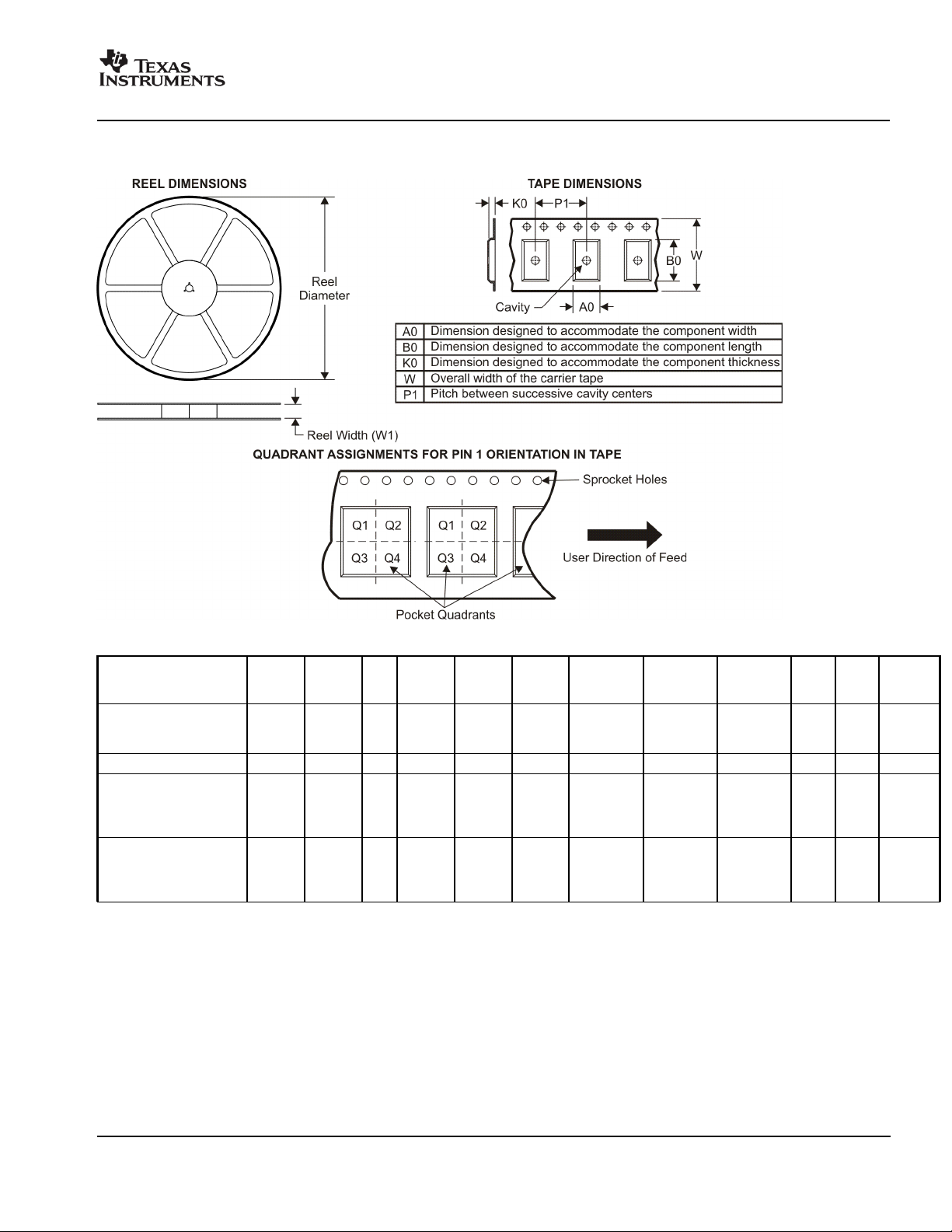
TAPE AND REEL INFORMATION
19-Mar-2008
*All dimensions are nominal
Device Package
Type
TPA6203A1DGNR MSOP-
Power
TPA6203A1DRBR SON DRB 8 3000 330.0 12.4 3.3 3.3 1.1 8.0 12.0 Q2
TPA6203A1GQVR BGA MI
CROSTA
R JUNI
TPA6203A1ZQVR BGA MI
CROSTA
R JUNI
PAD
OR
OR
Package
Drawing
DGN 8 2500 330.0 12.4 5.3 3.4 1.4 8.0 12.0 Q1
GQV 8 2500 330.0 8.4 2.3 2.3 1.4 4.0 8.0 Q1
Pins SPQ Reel
Diameter
(mm)
ZQV 8 2500 330.0 8.4 2.3 2.3 1.4 4.0 8.0 Q1
Reel
Width
W1 (mm)
A0 (mm) B0 (mm) K0 (mm) P1
(mm)W(mm)
Pin1
Quadrant
Pack Materials-Page 1
PACKAGE MATERIALS INFORMATION
www.ti.com
19-Mar-2008
*All dimensions are nominal
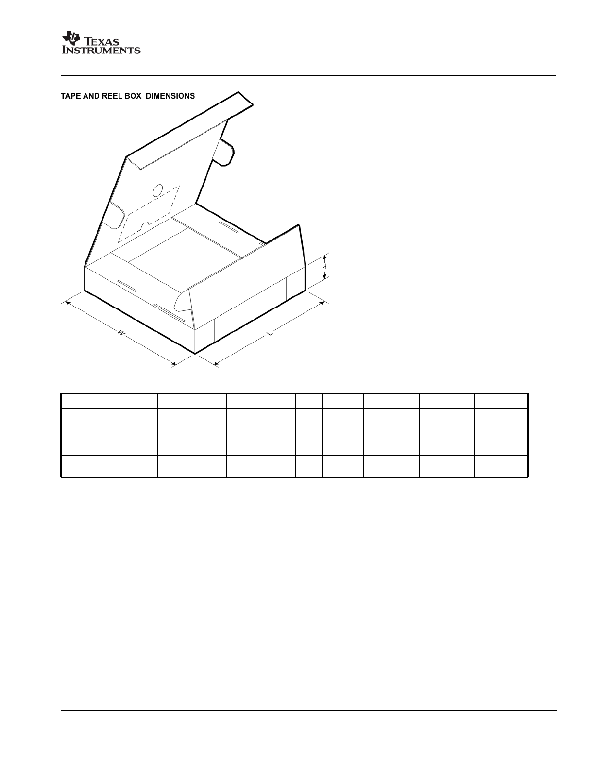
Device Package Type Package Drawing Pins SPQ Length (mm) Width (mm) Height (mm)
TPA6203A1DGNR MSOP-PowerPAD DGN 8 2500 346.0 346.0 29.0
TPA6203A1DRBR SON DRB 8 3000 346.0 346.0 29.0
TPA6203A1GQVR BGA MICROSTAR
JUNIOR
TPA6203A1ZQVR BGA MICROSTAR
JUNIOR
GQV 8 2500 340.5 333.0 20.6
ZQV 8 2500 340.5 333.0 20.6
Pack Materials-Page 2

MECHANICAL DATA
MPBG144C – JUNE 2000 – REVISED FEBRUARY 2002
GQV (S-PBGA-N8) PLASTIC BALL GRID ARRAY
2,10
1,90
SQ
C
1,00 TYP
0,50
A1 Corner
0,77
0,71
0,35
0,25
∅ 0,05
NOTES: A. All linear dimensions are in millimeters.
B. This drawing is subject to change without notice.
C. MicroStar Junior configuration
D. Falls within JEDEC MO-225
M
1,00 MAX
0,25
0,15
Seating Plane
0,08
B
A
1
23
Bottom View
1,00 TYP
0,50
4201040/E 01/02
MicroStar Junior is a trademark of Texas Instruments.
POST OFFICE BOX 655303 • DALLAS, TEXAS 75265


IMPORTANT NOTICE
Texas Instruments Incorporated and its subsidiaries (TI) reserve the right to make corrections, modifications, enhancements, improvements,
and other changes to its products and services at any time and to discontinue any product or service without notice. Customers should
obtain the latest relevant information before placing orders and should verify that such information is current and complete. All products are
sold subject to TI’s terms and conditions of sale supplied at the time of order acknowledgment.
TI warrants performance of its hardware products to the specifications applicable at the time of sale in accordance with TI’s standard
warranty. Testing and other quality control techniques are used to the extent TI deems necessary to support this warranty. Except where
mandated by government requirements, testing of all parameters of each product is not necessarily performed.
TI assumes no liability for applications assistance or customer product design. Customers are responsible for their products and
applications using TI components. To minimize the risks associated with customer products and applications, customers should provide
adequate design and operating safeguards.
TI does not warrant or represent that any license, either express or implied, is granted under any TI patent right, copyright, mask work right,
or other TI intellectual property right relating to any combination, machine, or process in which TI products or services are used. Information
published by TI regarding third-party products or services does not constitute a license from TI to use such products or services or a
warranty or endorsement thereof. Use of such information may require a license from a third party under the patents or other intellectual
property of the third party, or a license from TI under the patents or other intellectual property of TI.
Reproduction of TI information in TI data books or data sheets is permissible only if reproduction is without alteration and is accompanied
by all associated warranties, conditions, limitations, and notices. Reproduction of this information with alteration is an unfair and deceptive
business practice. TI is not responsible or liable for such altered documentation. Information of third parties may be subject to additional
restrictions.
Resale of TI products or services with statements different from or beyond the parameters stated by TI for that product or service voids all
express and any implied warranties for the associated TI product or service and is an unfair and deceptive business practice. TI is not
responsible or liable for any such statements.
TI products are not authorized for use in safety-critical applications (such as life support) where a failure of the TI product would reasonably
be expected to cause severe personal injury or death, unless officers of the parties have executed an agreement specifically governing
such use. Buyers represent that they have all necessary expertise in the safety and regulatory ramifications of their applications, and
acknowledge and agree that they are solely responsible for all legal, regulatory and safety-related requirements concerning their products
and any use of TI products in such safety-critical applications, notwithstanding any applications-related information or support that may be
provided by TI. Further, Buyers must fully indemnify TI and its representatives against any damages arising out of the use of TI products in
such safety-critical applications.
TI products are neither designed nor intended for use in military/aerospace applications or environments unless the TI products are
specifically designated by TI as military-grade or "enhanced plastic." Only products designated by TI as military-grade meet military
specifications. Buyers acknowledge and agree that any such use of TI products which TI has not designated as military-grade is solely at
the Buyer's risk, and that they are solely responsible for compliance with all legal and regulatory requirements in connection with such use.
TI products are neither designed nor intended for use in automotive applications or environments unless the specific TI products are
designated by TI as compliant with ISO/TS 16949 requirements. Buyers acknowledge and agree that, if they use any non-designated
products in automotive applications, TI will not be responsible for any failure to meet such requirements.
Following are URLs where you can obtain information on other Texas Instruments products and application solutions:
Products Applications
Amplifiers amplifier.ti.com Audio www.ti.com/audio
Data Converters dataconverter.ti.com Automotive www.ti.com/automotive
DSP dsp.ti.com Broadband www.ti.com/broadband
Clocks and Timers www.ti.com/clocks Digital Control www.ti.com/digitalcontrol
Interface interface.ti.com Medical www.ti.com/medical
Logic logic.ti.com Military www.ti.com/military
Power Mgmt power.ti.com Optical Networking www.ti.com/opticalnetwork
Microcontrollers microcontroller.ti.com Security www.ti.com/security
RFID www.ti-rfid.com Telephony www.ti.com/telephony
RF/IF and ZigBee® Solutions www.ti.com/lprf Video & Imaging www.ti.com/video
Mailing Address: Texas Instruments, Post Office Box 655303, Dallas, Texas 75265
Copyright © 2008, Texas Instruments Incorporated
Wireless www.ti.com/wireless
 Loading...