

Page 1
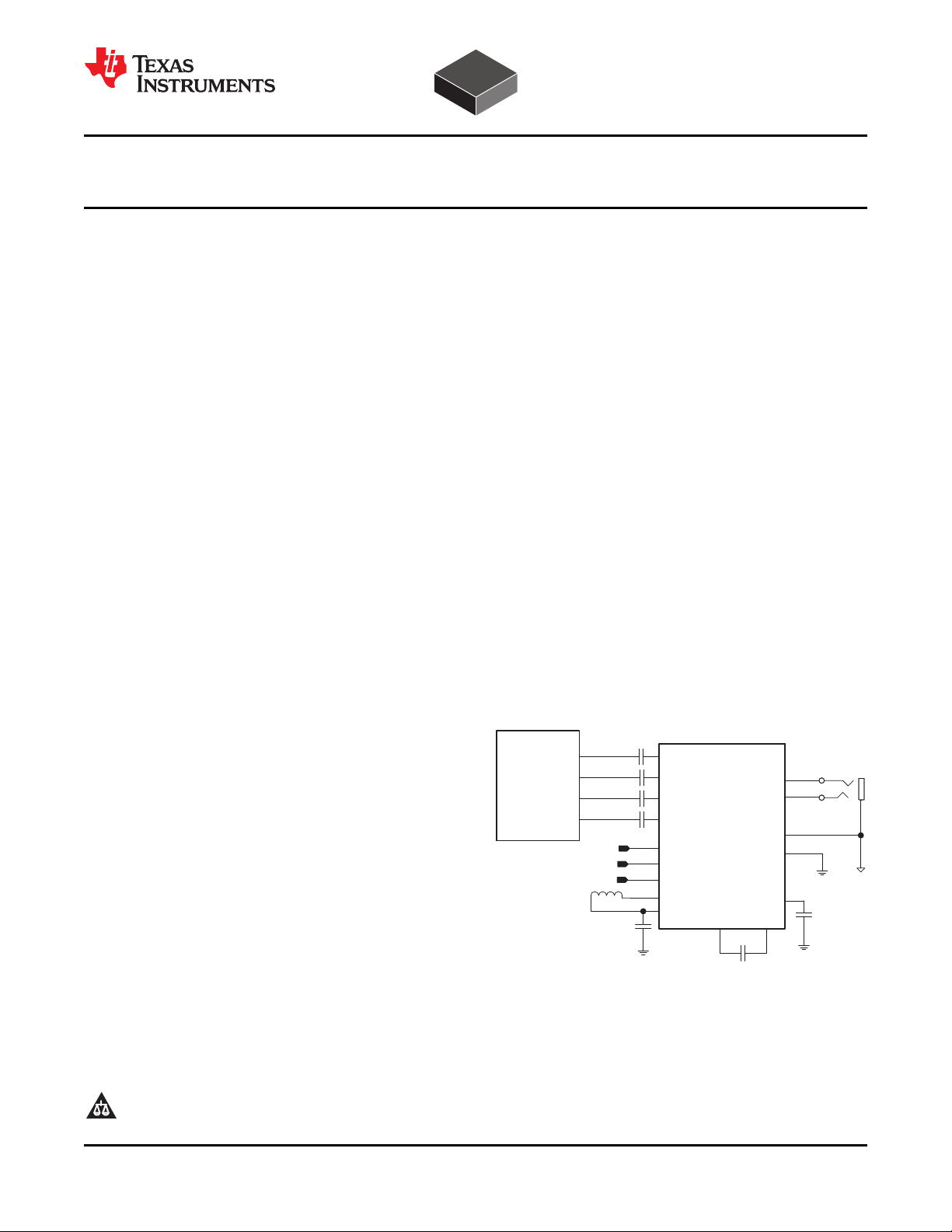
INR+
INR-
INL+
INL-
AGND
SGND
OUTR
HPVSS
CPP CPN
SW
HPVDD
OUTL
TPA6140A2
Vbat
CODEC
OUTR+
OUTR-
OUTL+
OUTL-
1 Fm
SDA
SCL SCL
AVDD
SDA
2.2 Hm
2.2 Fm
1 Fm
2.2 Fm
TPA6140A2
www.ti.com
.................................................................................................................................................................................................. SLOS598 – MARCH 2009
CLASS-G DIRECTPATH™ STEREO HEADPHONE AMPLIFIER
WITH I2C VOLUME CONTROL
1
FEATURES DESCRIPTION
2
• TI Class-G Technology Significantly Prolongs
Battery Life and Music Playback Time
– 0.6 mA / Ch Quiescent Current
– 50% to 80% Lower Quiescent Current than
Ground-Referenced Class-AB Headphone
Amplifiers
• DirectPath
Output DC-Blocking Capacitors
– Outputs Biased at 0 V
– Improves Low Frequency Audio Fidelity
• I2C Volume Control
– – 59 dB to +4 dB Gain
• Active Click and Pop Suppression
• Fully Differential Inputs Reduce System Noise
– Also Configurable as Single-Ended Inputs
• SGND Pin Eliminates Ground Loop Noise
• Wide Power Supply Range: 2.5 V to 5.5 V
• 100 dB Power Supply Noise Rejection
• Short-Circuit Current Limiter
• Thermal-Overload Protection
• Software Compatible with TPA6130A2
• 0,4 mm Pitch, 1,6 mm × 1,6 mm WCSP
Package
TM
Technology Eliminates Large
The TPA6140A2 (also known as TPA6140) is a
Class-G DirectPath™ stereo headphone amplifier
with built-in I2C volume control. Class-G technology
maximizes battery life by adjusting the voltage
supplies of the headphone amplifier based on the
audio signal level. At low level audio signals, the
internal supply voltage is reduced to minimize power
dissipation. DirectPath
TM
technology eliminates
external DC-blocking capacitors.
The device operates from a 2.5 V to 5.5 V supply
voltage. Class-G operation keeps total supply current
below 5.0 mA while delivering 500 µ W per channel
into 32 Ω . Shutdown mode reduces the supply
current to less than 3 µ A and is activated through the
I2C interface.
The TPA6140A2 (TPA6140) I2C register map is
compatible to the TPA6130A2, simplifying software
development.
The amplifier outputs have short-circuit and
thermal-overload protection along with ± 8 kV HBM
ESD protection, simplifying end equipment
compliance to the IEC 61000-4-2 ESD standard.
The TPA6140A2 (TPA6140) is available in a 0,4 mm
pitch, 16-bump 1,6 mm × 1,6 mm WCSP (YFF)
package.
APPLICATIONS
• Cellular Phones / Music Phones
• Portable Media / MP3 Players
• Portable CD / DVD Players
1
2 Class-G DirectPath, DirectPath are trademarks of Texas Instruments.
PRODUCTION DATA information is current as of publication date.
Products conform to specifications per the terms of the Texas
Instruments standard warranty. Production processing does not
necessarily include testing of all parameters.
Please be aware that an important notice concerning availability, standard warranty, and use in critical applications of Texas
Instruments semiconductor products and disclaimers thereto appears at the end of this data sheet.
Copyright © 2009, Texas Instruments Incorporated
Page 2
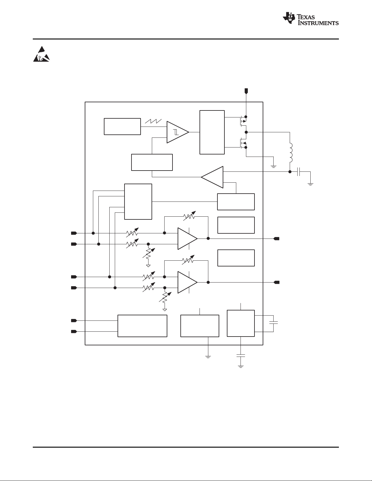
Thermal
Protection
SDA
I2CInterface
SCL
Click-and-Pop
Suppression
Charge
Pump
1 Fm
CPP
CPN
HPVSSSGND
Short-Circuit
Protection
+
–
HPVDD
HPVSS
+
–
HPVDD
HPVSS
OUTL
OUTR
INR+
INR-
INL+
INL-
+
–
Gate
Drivers
AVDD
Optimizer
Ramp
Generator
+
–
Comparator
Audio
Level
Detector
AGND
2.2 Fm
SW
AVDD
HPVDD
HPVDD
HPVDD
Compensation
Network
2.2 Hm
2.2 Fm
TPA6140A2
SLOS598 – MARCH 2009 ..................................................................................................................................................................................................
These devices have limited built-in ESD protection. The leads should be shorted together or the device placed in conductive foam
during storage or handling to prevent electrostatic damage to the MOS gates.
www.ti.com
FUNCTIONAL BLOCK DIAGRAM
2 Copyright © 2009, Texas Instruments Incorporated
Product Folder Link(s): TPA6140A2
Page 3
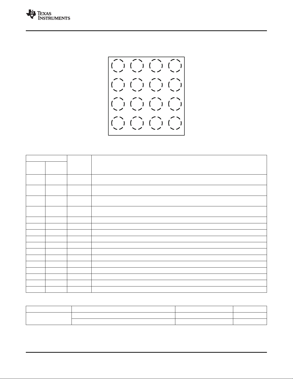
D1 D2 D3 D4
C1 C2 C3 C4
B1 B2 B3 B4
A1 A3 A4
SW
AGND
CPN
SDA
AVDD
CPP
HPVSS
SCL
OUTL
HPVDD
OUTR
INL-
INL+
INR+
A2
SGND
INR-
WCSP PACKAGE
(TOPVIEW)
TPA6140A2
www.ti.com
.................................................................................................................................................................................................. SLOS598 – MARCH 2009
DEVICE PINOUT
TERMINAL INPUT /
NAME
INL – A4 I Inverting left input for differential signals; connect to left input signal through 1 µ F capacitor for
INL+ B4 I Non-inverting left input for differential signals; connect to ground through 1 µ F capacitor for
INR – C4 I Inverting right input for differential signals; connect to right input signal through 1 µ F capacitor for
INR+ D4 I Non-inverting right input for differential signals; connect to ground through 1 µ F capacitor for
SGND C3 I Sense Ground; connect to shield terminal of headphone jack or to AGND
SDA D1 I/O I2C Data; 1.8 V logic compliant
SCL D2 I I2C Clock; 1.8 V logic compliant
OUTL A3 O Left headphone amplifier output; connect to left terminal of headphone jack
OUTR D3 O Right headphone amplifier output; connect to right terminal of headphone jack
CPP B2 P Charge pump positive flying cap; connect to positive side of capacitor between CPP and CPN
CPN C1 P Charge pump negative flying cap; connect to negative side of capacitor between CPP and CPN
SW A1 P Buck converter switching node
AVDD A2 P Primary power supply for device
HPVDD B3 P Power supply for headphone amplifier (DC/DC output node)
AGND B1 P Main Ground for headphone amplifiers, DC/DC converter, and charge pump
HPVSS C2 P Charge pump output; connect 2.2 µ F capacitor to GND
– 40 ° C to 85 ° C
(1) For the most current package and ordering information, see the Package Option Addendum at the end of this document, or see the TI
Web site at www.ti.com .
(2) YFF packages are only available taped and reeled. The suffix “ R ” indicates a reel of 3000, the suffix “ T ” indicates a reel of 250.
BALL
WCSP
T
A
OUTPUT /
POWER
(I/O/P)
TERMINAL FUNCTIONS
DESCRIPTION
single-ended input applications
single-ended input applications
single-ended input applications
single-ended input applications
ORDERING INFORMATION
PACKAGED DEVICES
16-ball, 1,6 mm × 1,6 mm WCSP TPA6140A2YFFR AIFI
16-ball, 1,6 mm × 1,6 mm WCSP TPA6140A2YFFT AIFI
(1)
PART NUMBER
(2)
SYMBOL
Copyright © 2009, Texas Instruments Incorporated 3
Product Folder Link(s): TPA6140A2
Page 4
TPA6140A2
SLOS598 – MARCH 2009 ..................................................................................................................................................................................................
ABSOLUTE MAXIMUM RATINGS
(1)
over operating free-air temperature range, TA= 25 ° C (unless otherwise noted)
VALUE / UNIT
Supply voltage, AVDD – 0.3 V to 6.0 V
Amplifier supply voltage, HPVDD – 0.3 V to 2.0 V
V
Input voltage – 0.3 V to HPV
I
I2C voltage – 0.3 V to AVDD
Output continuous total power dissipation See Dissipation Rating Table
T
Operating free-air temperature range – 40 ° C to 85 ° C
A
T
Operating junction temperature range – 40 ° C to 150 ° C
J
T
Storage temperature range – 65 ° C to 85 ° C
stg
Lead temperature 1,6 mm (1/16 inch) from case for 10 seconds 260 ° C
ESD Protection – HBM
(1) Stresses beyond those listed under absolute maximum ratings may cause permanent damage to the device. These are stress ratings
only, and functional operation of the device at these or any other conditions beyond those indicated under recommended operating
conditions is not implied. Exposure to absolute – maximum – rated conditions for extended periods may affect device reliability.
PACKAGE
POWER RATING ABOVE TA= POWER RATING POWER RATING
YFF (WCSP) 1.25 W 10 mW/ ° C 800 mW 650 mW
OUTL, OUTR, SGND 8 kV
All other pins 2 kV
DISSIPATION RATINGS TABLE
(1) (2)
OPERATING
TA< 25 ° C FACTOR TA= 70 ° C TA= 85 ° C
25 ° C
www.ti.com
+0.3 V
DD
(1) Derating factor measured with JEDEC High K board: 1S0P – One signal layer and zero plane layers.
(2) See JEDEC Standard 51-3 for Low-K board, JEDEC Standard 51-7 for High-K board, and JEDEC
Standard 51-12 for using package thermal information. See JEDEC document page for downloadable
copies: http://www.jedec.org/download/default.cfm .
RECOMMENDED OPERATING CONDITIONS
Supply voltage, AV
V
High-level input voltage SDA, SCL 1.3 V
IH
V
Low-level input voltage SDA, SCL 0.35 V
IL
Voltage applied to Output; OUTR, OUTL (when SWS = 1, device disabled) – 0.3 3.6 V
Voltage applied to Output; OUTR, OUTL (when SWS = 0, HiZ_L = HiZ_R = 1, device in HI-Z mode) – 1.8 1.8 V
T
Operating free-air temperature – 40 85 ° C
A
DD
MIN MAX UNIT
2.5 5.5 V
4 Copyright © 2009, Texas Instruments Incorporated
Product Folder Link(s): TPA6140A2
Page 5
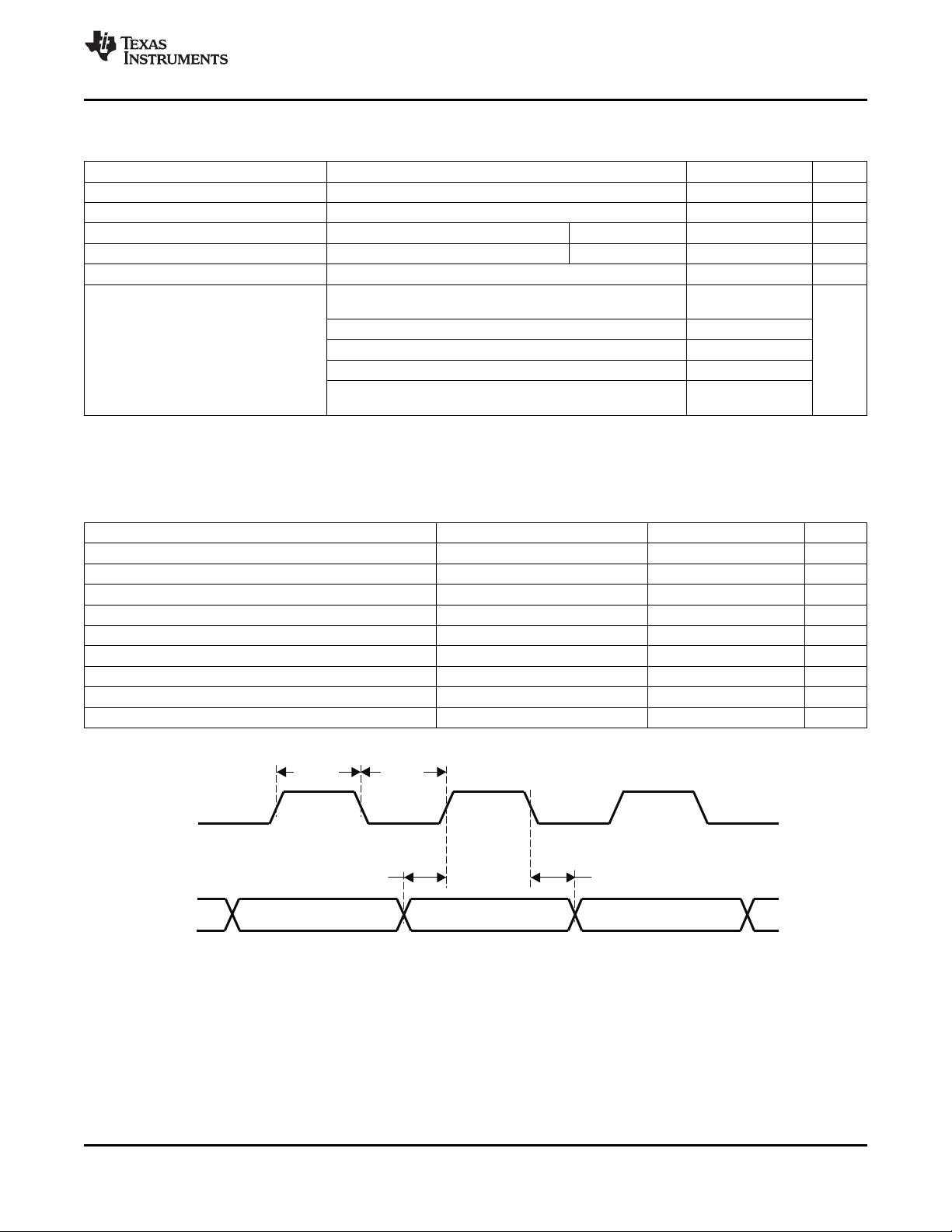
SCL
SDA
t
w(H)
t
w(L)
t
su1
t
h1
TPA6140A2
www.ti.com
.................................................................................................................................................................................................. SLOS598 – MARCH 2009
ELECTRICAL CHARACTERISTICS
TA= 25 ° C (unless otherwise noted)
PARAMETER TEST CONDITIONS MIN TYP MAX UNIT
PSRR Power supply rejection ratio AV
CMRR Common-mode rejection ratio HPV
|IIH| High-level input current AV
|IIL| Low-level input current AV
I
SD
I
DD
Soft shutdown current SW Shutdown mode, V
Total supply current AV
(1) Per channel output power assuming a 10 dB crest factor
= 2.5 V to 5.5 V, inputs grounded, GAIN = 0 dB 90 105 dB
DD
= 1.3 V to 1.8 V, GAIN = 0 dB 68 dB
DD
= 2.5 V to 5.5 V, VI= AV
DD
= 2.5 V to 5.5 V, VI= 0 V SCL, SDA 1 µ A
DD
AV
= 3.6 V HPVDD = 1.3 V, Amplifiers active, no load, no
DD
input signal
AV
= 3.6 V, P
DD
= 3.6 V, P
DD
AV
= 3.6 V, P
DD
AV
= 3.6 V, HiZ_L = HiZ_R = HIGH (High output impedance
DD
mode)
= 100 µ W into 32 Ω
OUT
= 500 µ W into 32 Ω
OUT
= 1 mW into 32 Ω
OUT
DD
= 2.5 V to 5.5 V, SWS bit = 1 1 3 µ A
DD
(1)
TIMING CHARACTERISTICS
For I2C interface signals over recommended operating conditions (unless otherwise noted)
PARAMETER TEST CONDITIONS MIN TYP MAX UNIT
f
t
t
t
t
t
t
t
t
Frequency, SCL No wait states 400 kHz
SCL
Pulse duration, SCL high 0.6 µ s
W(H)
Pulse duration, SCL low 1.3 µ s
W(L)
Setup time, SDA to SCL 100 µ s
SU1
Hold time, SCL to SDA 10 ns
H1
Bus free time between stop and start condition 1.3 µ s
(BUF)
Setup time, SCL to start condition 0.6 µ s
SU2
Hold time, start condition to SCL 0.6 µ s
H2
Setup time, SCL to stop condition 0.6 µ s
SU3
SCL, SDA 1 µ A
1.2 2.0
(1)
, f
= 1 kHz 2.5
AUD
(1)
, f
= 1 kHz 4.0 mA
AUD
, f
= 1 kHz 6.8
AUD
1.0 2.0
Figure 1. SCL and SDA Timing
Product Folder Link(s): TPA6140A2
Copyright © 2009, Texas Instruments Incorporated 5
Page 6
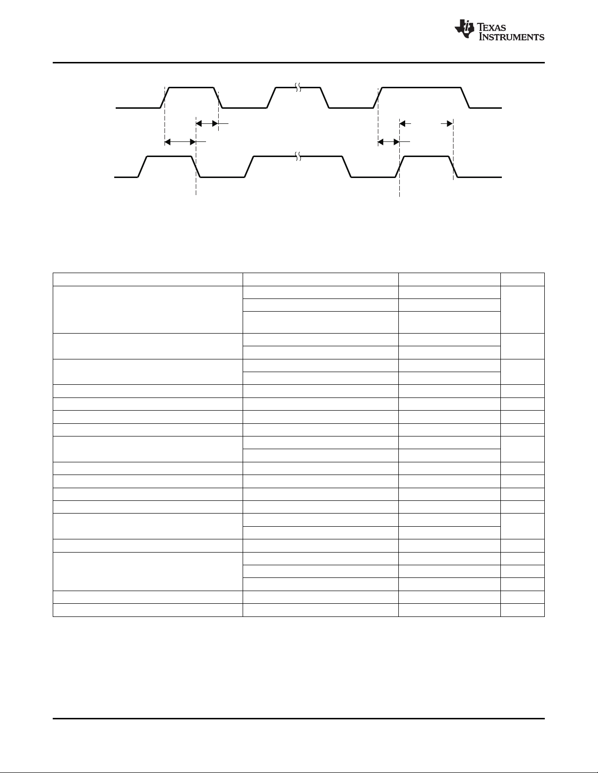
SCL
SDA
th2 t(buf)
tsu2 tsu3
StartCondition
StopCondition
TPA6140A2
SLOS598 – MARCH 2009 ..................................................................................................................................................................................................
Figure 2. Start and Stop Conditions Timing
OPERATING CHARACTERISTICS
AV
= 3.6 V , TA= 25 ° C, GAIN = 0 dB, RL= 32 Ω (unless otherwise noted)
DD
PARAMETER TEST CONDITIONS MIN TYP MAX UNIT
AV
P
O
Output power
(1)
(Outputs in Phase) mW
THD+N Total harmonic distortion plus noise
k
SVR
Δ A
V
V
OS
E
n
f
BUCK
f
PUMP
AC-Power supply rejection ratio dB
Gain matching Between left and right channels 1%
Output offset voltage AV
Noise output voltage A-weighted 5.3 µ V
Buck converter switching frequency PO= 0.5 mW into 32 Ω , f = 1 kHz 600 kHz
Charge pump switching frequency kHz
Start-up time from shutdown 5 ms
R
IN,SE
R
IN,DF
Single Ended Input impedance Gain = 4 dB, per input node 15.6 k Ω
Differential input impedance Gain = 4 dB, per input node 31.2 k Ω
SNR Signal-to-noise ratio V
Thermal shutdown ° C
Z
O,SD
Z
O,HI-Z
Output impedance in shutdown SWS = 1, DC value 8 k Ω
Output impedance in Hi-Z mode 6 MHz, 1.8 V
Crosstalk PO= 15 mW, f = 1 kHz – 80 dB
V
CM
Input common-mode voltage range 0 1.4 V
(1) Per channel output power
(2) A-weighted
AV
AV
16 Ω
PO= 10 mW into 16 Ω , f = 1 kHz 0.02%
(2)
PO= 20 mW into 32 Ω , f = 1 kHz 0.01%
200 mVpp ripple, f = 217 Hz 80 100
200 mVpp ripple, f = 4 kHz 90
PO= 0.5 mW into 32 Ω , f = 1 kHz 315
PO= 15 mW into 32 Ω , f = 1 kHz 1260
Threshold 165
Hysteresis 35
40 kHz, 1.8 V
13 MHz, 1.8 V
= 2.7V, THD = 1%, f = 1 kHz 26
DD
= 2.7V, THD = 10%, f = 1 kHz 32
DD
= 2.7V, THD = 1%, f = 1 kHz, RL=
DD
= 2.5 V to 5.5 V, inputs grounded – 0.5 0 0.5 mV
DD
= 1 V
OUT
, GAIN = 4 dB, no load 105 dB
RMS
signal max 8.5 k Ω
PEAK
signal max 600 Ω
PEAK
signal max 400 Ω
PEAK
25
www.ti.com
RMS
6 Copyright © 2009, Texas Instruments Incorporated
Product Folder Link(s): TPA6140A2
Page 7
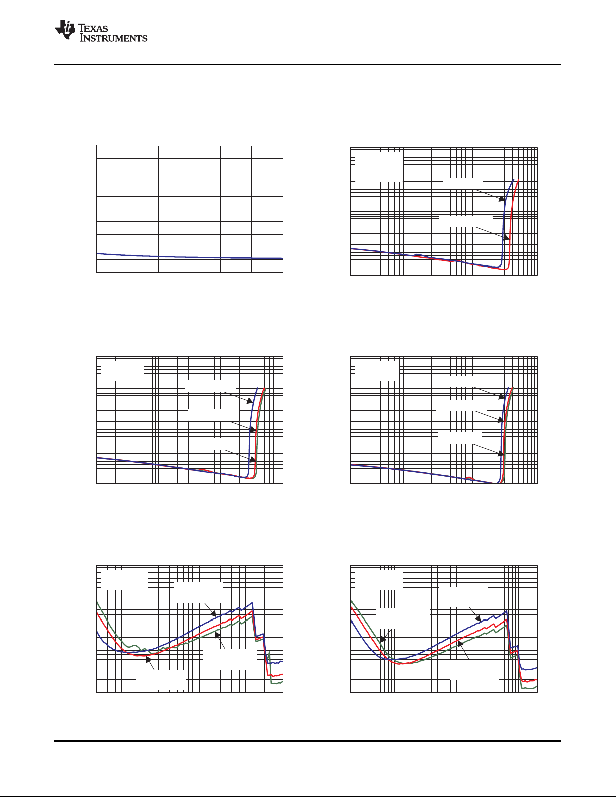
VDD − Supply Voltage − V
0
1
2
3
4
5
6
7
8
9
10
2.5 3.0 3.5 4.0 4.5 5.0 5.5
Quiescent Supply Current − mA
G001
PO − Output Power − W
f = 1 kHz
RL = 16 Ω
VDD = 3.6 V
THD+N − T otal Harmonic Distortion + Noise − %
0.0001 0.001 0.01 0.1
100
1
0.1
0.01
G002
10
Out of Phase
In Phase
PO − Output Power − W
f = 1 kHz
RL = 16 Ω
THD+N − T otal Harmonic Distortion + Noise − %
0.0001 0.001 0.01 0.1
100
1
0.1
0.01
G003
10
VDD = 2.5 V
VDD = 3.6 V
VDD = 5 V
PO − Output Power − W
f = 1 kHz
RL = 32 Ω
THD+N − T otal Harmonic Distortion + Noise − %
0.0001 0.001 0.01 0.1
100
1
0.1
0.01
G004
10
VDD = 2.5 V
VDD = 3.6 V
VDD = 5 V
f − Frequency − Hz
RL = 16 Ω
VDD = 2.5 V
THD+N − T otal Harmonic Distortion + Noise − %
20 100 1k 20k
1
0.1
0.01
0.001
G005
10k
PO = 1 mW
per Channel
PO = 10 mW
per Channel
PO = 4 mW
per Channel
f − Frequency − Hz
RL = 32 Ω
VDD = 2.5 V
THD+N − T otal Harmonic Distortion + Noise − %
20 100 1k 20k
1
0.1
0.01
0.001
G006
10k
PO = 1 mW
per Channel
PO = 4 mW
per Channel
PO = 10 mW
per Channel
TPA6140A2
www.ti.com
.................................................................................................................................................................................................. SLOS598 – MARCH 2009
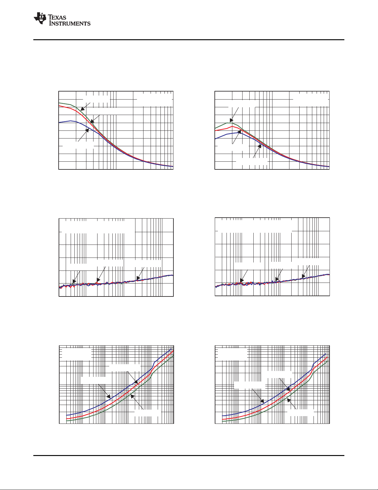
TYPICAL CHARACTERISTICS
TA= 25 ° C, AV
(V
) = 3.6 V, GAIN = 0 dB, C
DD
DD
= C
HPVDD
HPVSS
= 2.2 µ F, C
= C
INPUT
= 1 µ F, Outputs out of phase
FLYING
QUIESCENT SUPPLY CURRENT TOTAL HARMONIC DISTORTION + NOISE
vs vs
SUPPLY VOLTAGE OUTPUT POWER
Figure 3. Figure 4.
TOTAL HARMONIC DISTORTION + NOISE TOTAL HARMONIC DISTORTION + NOISE
vs vs
OUTPUT POWER OUTPUT POWER
Figure 5. Figure 6.
TOTAL HARMONIC DISTORTION + NOISE TOTAL HARMONIC DISTORTION + NOISE
FREQUENCY FREQUENCY
Copyright © 2009, Texas Instruments Incorporated 7
Figure 7. Figure 8.
vs vs
Product Folder Link(s): TPA6140A2
Page 8
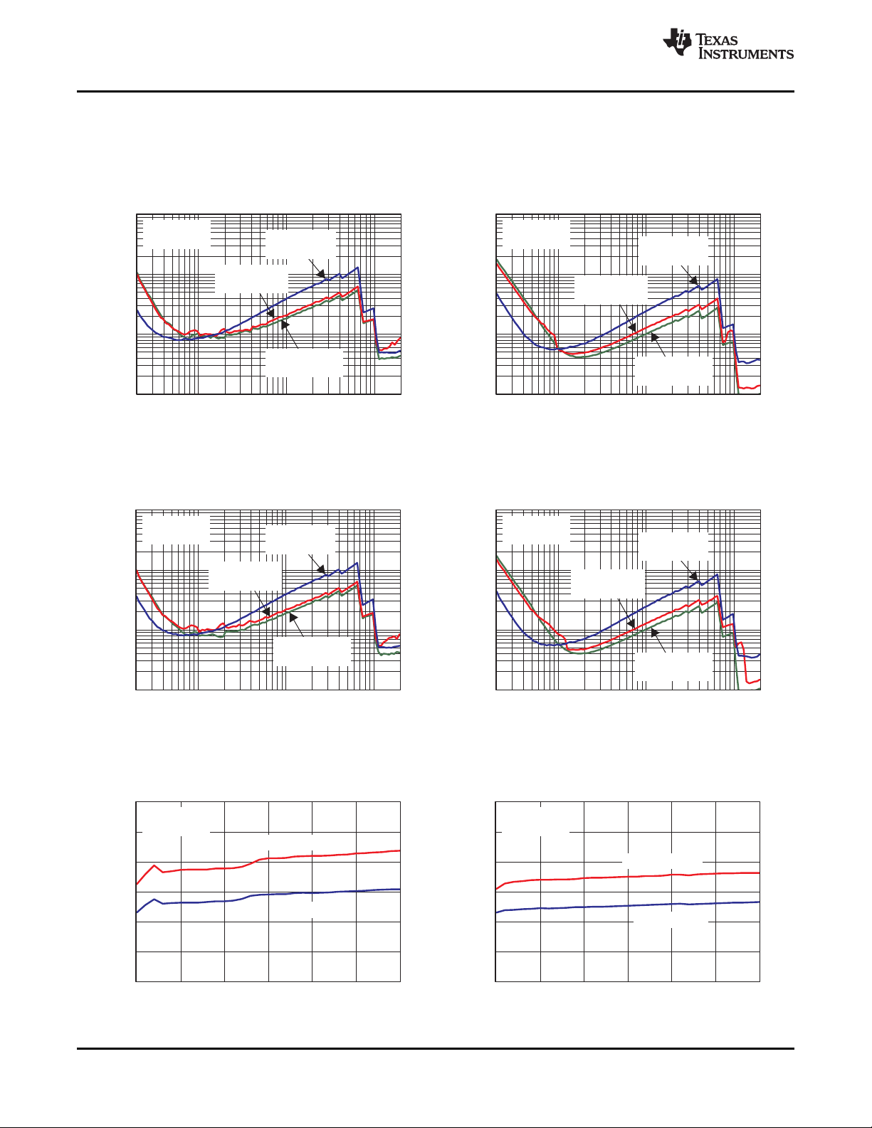
f − Frequency − Hz
RL = 16 Ω
VDD = 3.6 V
THD+N − T otal Harmonic Distortion + Noise − %
20 100 1k 20k
1
0.1
0.01
0.001
G007
10k
PO = 1 mW
per Channel
PO = 10 mW
per Channel
PO = 15 mW
per Channel
f − Frequency − Hz
RL = 32 Ω
VDD = 3.6 V
THD+N − T otal Harmonic Distortion + Noise − %
20 100 1k 20k
1
0.1
0.01
0.001
G008
10k
PO = 1 mW
per Channel
PO = 20 mW
per Channel
PO = 10 mW
per Channel
f − Frequency − Hz
RL = 16 Ω
VDD = 5 V
THD+N − T otal Harmonic Distortion + Noise − %
20 100 1k 20k
1
0.1
0.01
0.001
G009
10k
PO = 1 mW
per Channel
PO = 15 mW
per Channel
PO = 10 mW
per Channel
f − Frequency − Hz
RL = 32 Ω
VDD = 5 V
THD+N − T otal Harmonic Distortion + Noise − %
20 100 1k 20k
1
0.1
0.01
0.001
G010
10k
PO = 1 mW
per Channel
PO = 20 mW
per Channel
PO = 10 mW
per Channel
VDD − Supply Voltage − V
0
10
20
30
40
50
60
2.5 3.0 3.5 4.0 4.5 5.0 5.5
P
O
− Output Power per Channel − mW
G011
THD+N = 1%
THD+N = 10%
RL = 16 Ω
In Phase
VDD − Supply Voltage − V
0
10
20
30
40
50
60
2.5 3.0 3.5 4.0 4.5 5.0 5.5
P
O
− Output Power per Channel − mW
G012
THD+N = 1%
THD+N = 10%
RL = 32 Ω
In Phase
TPA6140A2
SLOS598 – MARCH 2009 ..................................................................................................................................................................................................
TA= 25 ° C, AV
TYPICAL CHARACTERISTICS (continued)
(V
) = 3.6 V, GAIN = 0 dB, C
DD
DD
TOTAL HARMONIC DISTORTION + NOISE TOTAL HARMONIC DISTORTION + NOISE
vs vs
FREQUENCY FREQUENCY
Figure 9. Figure 10.
TOTAL HARMONIC DISTORTION + NOISE TOTAL HARMONIC DISTORTION + NOISE
vs vs
FREQUENCY FREQUENCY
= C
HPVDD
HPVSS
= 2.2 µ F, C
= C
INPUT
= 1 µ F, Outputs out of phase
FLYING
www.ti.com
Figure 11. Figure 12.
OUTPUT POWER PER CHANNEL OUTPUT POWER PER CHANNEL
SUPPLY VOLTAGE SUPPLY VOLTAGE
8 Copyright © 2009, Texas Instruments Incorporated
Figure 13. Figure 14.
vs vs
Product Folder Link(s): TPA6140A2
Page 9
RL − Load Resistance − Ω
0
5
10
15
20
25
30
35
40
45
50
THD+N = 1%
Out of Phase
P
O
− Output Power − mW
10 100 1k
G013
VDD = 5 V
VDD = 2.5 V
VDD = 3.6 V
RL − Load Resistance − Ω
0
5
10
15
20
25
30
35
40
45
50
THD+N = 1%
In Phase
P
O
− Output Power − mW
10 100 1k
G014
VDD = 5 V
VDD = 2.5 V
VDD = 3.6 V
f − Frequency − Hz
−120
−100
−80
−60
−40
−20
0
RL = 32 Ω
Supply Ripple = 0.2 V
pp
Sine Wave
20 100 1k 20k
G016
10k
k
SVR
− Supply Ripple Rejection Ratio− dB
VDD = 2.5 V
VDD = 5 V
VDD = 3.6 V
f − Frequency − Hz
−120
−100
−80
−60
−40
−20
0
RL = 16 Ω
Supply Ripple = 0.2 V
pp
Sine Wave
20 100 1k 20k
G015
10k
k
SVR
− Supply Ripple Rejection Ratio − dB
VDD = 5 V
VDD = 3.6 V
VDD = 2.5 V
PO − T otal Output Power − mW
f = 1 kHz
RL = 16 Ω
0.001 0.01 100
100
10
1
G017
100.1
VDD = 2.5 V
1
VDD = 3.6 V
VDD = 5 V
I
DD
− Supply Current − mA
PO − T otal Output Power − mW
f = 1 kHz
RL = 32 Ω
0.001 0.01 100
100
10
1
G018
100.1
VDD = 2.5 V
1
VDD = 3.6 V
VDD = 5 V
I
DD
− Supply Current − mA
TPA6140A2
www.ti.com
TA= 25 ° C, AV
.................................................................................................................................................................................................. SLOS598 – MARCH 2009
TYPICAL CHARACTERISTICS (continued)
(V
) = 3.6 V, GAIN = 0 dB, C
DD
DD
OUTPUT POWER OUTPUT POWER
vs vs
LOAD RESISTANCE LOAD RESISTANCE
Figure 15. Figure 16.
SUPPLY RIPPLE REJECTION RATIO SUPPLY RIPPLE REJECTION RATIO
vs vs
FREQUENCY FREQUENCY
= C
HPVDD
HPVSS
= 2.2 µ F, C
= C
INPUT
= 1 µ F, Outputs out of phase
FLYING
Figure 17. Figure 18.
SUPPLY CURRENT SUPPLY CURRENT
TOTAL OUTPUT POWER TOTAL OUTPUT POWER
Copyright © 2009, Texas Instruments Incorporated 9
Figure 19. Figure 20.
vs vs
Product Folder Link(s): TPA6140A2
Page 10

VDD − Supply Voltage − V
0.0
0.2
0.4
0.6
0.8
1.0
1.2
1.4
1.6
1.8
2.0
2.5 3.0 3.5 4.0 4.5 5.0 5.5
f = 1 kHz
THD+N = 1%
V
O
− Output Voltage − V rms
G020
RL = 1 kΩ
RL = 600 Ω
RL = 16 Ω
RL = 32 Ω
PO − T otal Output Power − mW
0.01 0.1 1 100
G019
10
RL = 16 Ω
P
T
− T otal Power Dissipation − W
1k
100
10
1
RL = 32 Ω
f − Frequency − Hz
−100
−80
−60
−40
−20
0
RL = 16 Ω
PO = 15 mW
20 100 1k 20k
G021
10k
Crosstalk − dB
f − Frequency − Hz
−150
−120
−90
−60
−30
0
0 5000 10000 15000 20000
Single Channel
RL = 16 Ω
V
O
− Output Amplitude − dBV
G022
t − Time − ms
−1
0
1
2
3
4
5
0 1 2 3 4 5 6 7 8 9 10
V − Voltage − V
G023
SDA
V
OUT
Enable
RL = 16 Ω
VIN = 0.5 Vrms @ 1 kHz
t − Time − µs
−1
0
1
2
3
4
5
0 50 100 150 200
RL = 16 Ω
VIN = 0.5 Vrms @ 20 kHz
V − Voltage − V
G024
SDA
V
OUT
Disable
TPA6140A2
SLOS598 – MARCH 2009 ..................................................................................................................................................................................................
TA= 25 ° C, AV
TYPICAL CHARACTERISTICS (continued)
(V
) = 3.6 V, GAIN = 0 dB, C
DD
DD
TOTAL POWER DISSIPATION OUTPUT VOLTAGE
vs vs
TOTAL OUTPUT POWER SUPPLY VOLTAGE
Figure 21. Figure 22.
CROSSTALK OUTPUT AMPLITUDE
vs vs
FREQUENCY FREQUENCY
= C
HPVDD
HPVSS
= 2.2 µ F, C
INPUT
www.ti.com
= C
= 1 µ F, Outputs out of phase
FLYING
Figure 23. Figure 24.
STARTUP WAVEFORM SHUTDOWN WAVEFORM
10 Copyright © 2009, Texas Instruments Incorporated
Figure 25. Figure 26.
vs vs
TIME TIME
Product Folder Link(s): TPA6140A2
Page 11

INR+
INR-
INL+
INL-
AGND
SGND
OUTR
HPVSS
CPP CPN
SW
HPVDD
OUTL
TPA6140A2
Vbat
CODEC
OUTR+
OUTR-
OUTL+
OUTL-
1 Fm
SDA
SCL SCL
AVDD
SDA
2.2 Fm
2.2 Fm
2.2 Hm
1 Fm
INR+
INR-
INL+
INL-
AGND
SGND
OUTR
HPVSS
CPP CPN
SW
HPVDD
OUTL
TPA6140A2
CODEC
OUTR
OUTL
SDA
SCL SCL
AVDD
SDA
Vbat
1 Fm
2.2 Fm
1 Fm
2.2 Hm
2.2 Fm
TPA6140A2
www.ti.com
APPLICATION CIRCUIT
.................................................................................................................................................................................................. SLOS598 – MARCH 2009
APPLICATION INFORMATION
Figure 27. Typical Apps Configuration with Differential Input Signals
Figure 28. Typical Apps Configuration with Single-Ended Input Signals
Copyright © 2009, Texas Instruments Incorporated 11
Product Folder Link(s): TPA6140A2
Page 12

LOAD RMS
LOAD
LOAD
V 200 mV
I 6.25 mA
R 32
= = =
W
SUP LOAD DDQ
I I I 7.25 mA= + =
SUP SUP SUP
P V I 4.2 V 7.25 mA 30.45 mW= ´ = ´ =
REG REG SUP
P V I 1.3 V 7.25 mA 9.425 mW= ´ = ´ =
REG
SUP
P
P 11.09 mW
90%
= =
TPA6140A2
SLOS598 – MARCH 2009 ..................................................................................................................................................................................................
www.ti.com
CLASS-G HEADPHONE AMPLIFIER
Class-G amplifiers use adaptive supply rails. The TPA6140A2 includes a built-in step-down converter to create
the headphone amplifier positive supply voltage, HPVDD. A charge pump inverts HPVDD and creates the
amplifier negative supply voltage, HPVSS. This allows the headphone amplifier output to be centered at 0 V and
eliminates DC blocking capacitors.
When audio signal amplitude is low, the step-down converter generates a low HPVDD voltage. This minimizes
TPA6140A2 power consumption while playing low amplitude, high fidelity audio. If audio amplitude increases,
either due to louder music or a transient peak, then the step-down converter generates a higher HPVDD voltage.
The HPVDD rise rate is faster than the audio peak rise time. This prevents audio distortion or clipping. Audio
quality and noise floor are not affected by HPVDD.
This adaptive HPVDD minimizes TPA6140A2 supply current while avoiding clipping and distortion. Because
normal listening levels are below 200 mV
has higher efficiency than traditional Class-AB headphone amplifiers.
The following equations compare a Class-AB amplifier to a Class-G amplifier. Both operate with identical battery
voltage, load impedance, and output voltage swing. For this study case, we assume a normal listening level of
200 mV
• P
SUP
• V
SUP
• I
SUP
• V
REG
• P
REG
• V
LOAD
• R
LOAD
• P
LOAD
• I
LOAD
Given an amplifier driving 200 mV
with no DirectPath™ in order to simplify the calculations.
RMS
: Supplied power
: Supply voltage
: Supply current
: DC/DC converter output voltage
: DC/DC converter output power
: Voltage across the load
: Load impedance
: Power dissipated at the load
: Current supplied to the load
into a 32 Ω load, the output current to the load is:
RMS
, HPVDD is most often at its lowest voltage. Thus, the TPA6140A2
RMS
Assuming a quiescent current of 1 mA (I
) the total current supplied to the amplifier is:
DDQ
The total power supplied to a Class-AB amplifier is then calculated as:
For a Class-G amplifier where the voltage rails are generated by a switching DC/DC converter, the supplied
power will depend on the DC/DC converter output voltage and efficiency. Assuming the DC/DC converter output
voltage is 1.3 V:
The total supplied power will be the DC/DC converter output power divided by the efficiency of the DC/DC
converter. Assuming 90% step-down efficiency, total power supplied to the Class-G amplifier is:
Class-G headphone amplifiers achieve much higher efficiency than equivalent Class-AB amplifiers.
(1)
(2)
(3)
(4)
(5)
12 Copyright © 2009, Texas Instruments Incorporated
Product Folder Link(s): TPA6140A2
Page 13
INR+
INR-
INL+
INL-
AGND
SGND
OUTR
HPVSS
CPP CPN
SW
HPVDD
OUTL
2.2 Fm
Vbat
CODEC
OUTR+
OUTR-
OUTL+
OUTL-
1mF
SDA
SCL SCL
AVDD
SDA
nHcoil
FM Tuner
2.2 Hm
2.2 Fm
TPA6140A2
TPA6140A2
www.ti.com
.................................................................................................................................................................................................. SLOS598 – MARCH 2009
INDUCTOR SELECTION
The TPA6140A2 requires one inductor for its DC/DC converter. The following table lists recommended inductors.
Inductors not shown on this table can be be used if they have similar performance characteristics.
When selecting an inductor observe the following rules:
• Lower DCR increases DC/DC converter efficiency.
• The minimum working inductance should never be below 1 µ H.
• Include temperature and aging derating factors into the inductor value calculations.
MANUFACTURER PART NUMBER
TOKO MDT2012-CH2R2A
Murata
Taiyo Yuden
LQM21PN2R2MC0D
LQH2MCN2R2M02L
BRL2012T2R2M
BRC1608T2R2M
GROUND SENSE FUNCTION
The ground sense pin, SGND, reduces ground-loop noise when the audio output jack is connected to a different
ground reference than codec and amplifier ground. Always connect the SGND pin to the headphone jack. This
reduces output offset voltage and eliminates turn-on pop. Figure 29 shows how to connect SGND when an FM
radio antenna function is implemented on the headphone wire. The nH coil and capacitor separate the RF signal
from the audio GND signal. In this case, SGND is used to eliminate the offset voltage that is generated from the
audio signal current and the RF coil low-frequency impedance.
The voltage difference between SGND and AGND cannot be greater than ± 300 mV. The amplifier performance
degrades if the voltage difference between SGND and AGND is greater than ± 300 mV.
Figure 29. Sense Ground
Copyright © 2009, Texas Instruments Incorporated 13
Product Folder Link(s): TPA6140A2
Page 14

+
–
VideoBuffer/Amp
(i.e.,THS7375)
TPA6140A2
75 W
OUTR
OUTL
C
L O
1
f
2 R C
=
p
O
C L
1
C
2 f R
=
p
TPA6140A2
SLOS598 – MARCH 2009 ..................................................................................................................................................................................................
www.ti.com
HIGH OUTPUT IMPEDANCE
The TPA6140A2 has a HI-Z bit option that increases output impedance while muting the amplifier. Set the HiZ_L
and HiZ_R bits (register 3, bits 1 and 0) to HIGH to activate the HI-Z mode. This feature allows the headphone
output jack to be shared for other functions besides audio. For example, sharing of a headphone jack between
audio and video as shown in Figure 30 . In HI-Z mode, the TPA6140A2 output impedance is high enough to
prevent video signal attenuation.
SWS BIT HI-Z BIT VOLTAGE ALLOWED ON COMMENTS
1 0 8 k Ω
1 1 8.5 k Ω
0 0 ≤ 1 Ω 1.2 mA – Active mode
0 1 600 Ω @ 6 MHz 1 mA – 1.8 V to 1.8 V HI-Z mode
(1) If AV
is < 3.3 V, then maximum allowed external voltage applied is AV
DD
OUTPUT SUPPLY
IMPEDANCE CURRENT
< 3 µ A – 0.3 V to 3.3 V
8.5 k Ω @ 40kHz
400 Ω @ 13 MHz
DD
MAXIMUM EXTERNAL
OUTPUT PINS
(1)
in this mode
Shutdown mode
HEADPHONE AMPLIFIERS
Single-supply headphone amplifiers typically require dc-blocking capacitors to remove dc bias from their output
voltage. The top drawing in Figure 31 illustrates this connection. If dc bias is not removed, large dc current will
flow through the headphones which wastes power, clips the output signal, and potentially damages the
headphones.
These dc-blocking capacitors are often large in value and size. Headphone speakers have a typical resistance
between 16 Ω and 32 Ω . This combination creates a high-pass filter with a cutoff frequency as shown in
Equation 6 , where R
For a given high-pass cutoff frequency and load impedance, the required dc-blocking capacitor is found as:
Reducing fCimproves low frequency fidelity and requires a larger dc-blocking capacitor. To achieve a 20 Hz
cutoff with 16 Ω headphones, C
consuming PCB area, increasing height, and increasing cost of assembly. During start-up or shutdown the
dc-blocking capacitor has to be charged or discharged. This causes an audible pop on start-up and power-down.
Large dc-blocking capacitors also reduce audio output signal fidelity.
14 Copyright © 2009, Texas Instruments Incorporated
Figure 30. Sharing One Connector Between Audio and Video Signals Example
is the load impedance, C
L
must be at least 500 µ F. Large capacitor values require large packages,
O
Product Folder Link(s): TPA6140A2
is the dc-blocking capacitor, and fCis the cutoff frequency.
O
(6)
(7)
Page 15

C
O
Conventional
V
OUT
GND
V
OUT
GND
V
BIAS
Capless
DirectPath™
GND
V
DD
V
SS
V
OUT
C
O
V
OUT
V
OUT
TPA6140A2
www.ti.com
.................................................................................................................................................................................................. SLOS598 – MARCH 2009
Two different headphone amplifier architectures are available to eliminate the need for dc-blocking capacitors.
The Capless amplifier architecture provides a reference voltage to the headphone connector shield pin as shown
in the middle drawing of Figure 31 . The audio output signals are centered around this reference voltage, which is
typically half of the supply voltage to allow symmetrical output voltage swing.
When using a Capless amplifier do not connect the headphone jack shield to any ground reference or large
currents will result. This makes Capless amplifiers ineffective for plugging non-headphone accessories into the
headphone connector. Capless amplifiers are useful only with floating GND headphones.
Figure 31. Amplifier Applications
The DirectPath™ amplifier architecture operates from a single supply voltage and uses an internal charge pump
to generate a negative supply rail for the headphone amplifier. The output voltages are centered around 0 V and
are capable of positive and negative voltage swings as shown in the bottom drawing of Figure 31 . DirectPath
amplifiers require no output dc-blocking capacitors. The headphone connector shield pin connects to ground and
will interface with headphones and non-headphone accessories. The TPA6140A2 is a DirectPath amplifier.
ELIMINATING TURN-ON POP AND POWER SUPPLY SEQUENCING
The TPA6140A2 has excellent noise and turn-on / turn-off pop performance. It uses an integrated click-and-pop
suppression circuit to allow fast start-up and shutdown without generating any voltage transients at the output
pins. Typical start-up time from shutdown is 5 ms.
DirectPath technology keeps the output dc voltage at 0 V even when the amplifier is powered up. The DirectPath
technology together with the active pop-and-click suppression circuit eliminates audible transients during start up
and shutdown.
Copyright © 2009, Texas Instruments Incorporated 15
Product Folder Link(s): TPA6140A2
Page 16

C
IN IN
1
f
2 R C
=
p
IN
C IN
1
C
2 f R
=
p
TPA6140A2
SLOS598 – MARCH 2009 ..................................................................................................................................................................................................
www.ti.com
Use input coupling capacitors to ensure inaudible turn-on pop. Activate the TPA6140A2 after all audio sources
have been activated and their output voltages have settled. During power-down, deactivate the TPA6140A2
before deactivating the audio input source.
RF AND POWER SUPPLY NOISE IMMUNITY
The TPA6140A2 employs a new differential amplifier architecture to achieve high power supply noise rejection
and RF noise rejection. RF and power supply noise are common in modern electronics. Although RF frequencies
are much higher than the 20 kHz audio band, signal modulation often falls in-band. This, in turn, modulates the
supply voltage, allowing a coupling path into the audio amplifier. A common example is the 217 Hz GSM
frame-rate buzz often heard from an active speaker when a cell phone is placed nearby during a phone call.
The TPA6140A2 has excellent rejection of power supply and RF noise, preventing audio signal degradation.
INPUT COUPLING CAPACITORS
Input coupling capacitors block any dc bias from the audio source and ensure maximum dynamic range. Input
coupling capacitors also minimize TPA6140A2 turn-on pop to an inaudible level.
The input capacitors are in series with TPA6140A2 internal input resistors, creating a high-pass filter. Equation 8
calculates the high-pass filter corner frequency. The input impedance, R
input capacitors decrease the corner frequency. See the Operating Characteristics table for input impedance
values.
, is dependent on device gain. Larger
IN
(8)
For a given high-pass cutoff frequency, the minimum input coupling capacitor is found as:
Example: Design for a 20 Hz corner frequency with a TPA6140A2 gain of +6 dB. The Operating Characteristics
table gives R
as 13.2 k Ω . Equation 9 shows the input coupling capacitors must be at least 0.6 µ F to achieve a
IN
20 Hz high-pass corner frequency. Choose a 0.68 µ F standard value capacitor for each TPA6140A2 input (X5R
material or better is required for best performance).
Input capacitors can be removed provided the TPA6140A2 inputs are driven differentially with less than ± 1 V
and the common-mode voltage is within the input common-mode range of the amplifier. Without input capacitors
turn-on pop performance may be degraded and should be evaluated in the system.
CHARGE PUMP FLYING CAPACITOR AND HPVSS CAPACITOR
The TPA6140A2 uses a built-in charge pump to generate a negative voltage supply for the headphone
amplifiers. The charge pump flying capacitor connects between CPP and CPN. It transfers charge to generate
the negative supply voltage. The HPVSS capacitor must be at least equal in value to the flying capacitor to allow
maximum charge transfer. Use low equivalent-series-resistance (ESR) ceramic capacitors (X5R material or
better is required for best performance) to maximize charge pump efficiency. Typical values are 1 µ F to 2.2 µ F
for the HPVSS and flying capacitors. Although values down to 0.47 µ F can be used, total harmonic distortion
(THD) will increase.
(9)
RMS
16 Copyright © 2009, Texas Instruments Incorporated
Product Folder Link(s): TPA6140A2
Page 17

TPA6140A2
www.ti.com
.................................................................................................................................................................................................. SLOS598 – MARCH 2009
POWER SUPPLY AND HPVDD DECOUPLING CAPACITORS AND CONNECTIONS
The TPA6140A2 DirectPath headphone amplifier requires adequate power supply decoupling to ensure that
output noise and total harmonic distortion (THD) remain low. Use good low equivalent-series-resistance (ESR)
ceramic capacitors (X5R material or better is required for best performance). Place a 2.2 µ F capacitor within
5 mm of the AVDD pin. Reducing the distance between the decoupling capacitor and AVDD minimizes parasitic
inductance and resistance, improving TPA6140A2 supply rejection performance. Use 0402 or smaller size
capacitors if possible. Ensure that the ground connection of each of the capacitors has a minimum length return
path to the device. Failure to properly decouple the TPA6140A2 may degrade audio or EMC performance.
For additional supply rejection, connect an additional 10 µ F or higher value capacitor between AVDD and
ground. This will help filter lower frequency power supply noise. The high power supply rejection ratio (PSRR) of
the TPA6140A2 makes the 10 µ F capacitor unnecessary in most applications.
Connect a 2.2 µ F capacitor between HPVDD and ground. This ensures the amplifier internal bias supply remains
stable and maximizes headphone amplifier performance.
WARNING:
DO NOT connect HPVDD directly to AVDD or an external supply voltage. The
voltage at HPVDD is generated internally. Connecting HPVDD to an external
voltage can damage the device.
LAYOUT RECOMMENDATIONS
GND CONNECTIONS
The SGND pin is an input reference and must be connected to the headphone ground connector pin. This
ensures no turn-on pop and minimizes output offset voltage. Do not connect more than ± 0.3 V to SGND.
AGND is a power ground. Connect supply decoupling capacitors for AVDD, HPVDD, and HPVSS to AGND.
GENERAL I2C OPERATION
The I2C bus employs two signals, SDA (data) and SCL (clock), to communicate between integrated circuits in a
system. The bus transfers data serially one bit at a time. The address and data 8-bit bytes are transferred most
significant bit (MSB) first. In addition, each byte transferred on the bus is acknowledged by the receiving device
with an acknowledge bit. Each transfer operation begins with the master device driving a start condition on the
bus and ends with the master device driving a stop condition on the bus. The bus uses transitions on the data
terminal (SDA) while the clock is at logic high to indicate start and stop conditions. A high-to-low transition on
SDA indicates a start and a low-to-high transition indicates a stop. Normal data-bit transitions bust occur within
the low time of the clock period. Figure 32 shows a typical sequence. The master generates the 7-bit slave
address and the read/write (R/W) bit to open communication with another device and then waits for an
acknowledge condition. The TPA6140A2 holds SDA low during the acknowledge clock period to indicate
acknowledgment. When this occurs, the master transmits the next byte of the sequence. Each device is
addressed by a unique 7-bit slave address plus R/W bit (1 byte). All compatible devices share the same signals
via a bidirectional bus using a wired-AND connection.
The TPA6140A2 operates as an I2C slave. The I2C voltage can not exceed the TPA6140A2 supply voltage,
AVDD.
An external pull-up resistor must be used for the SDA and SCL signals to set the logic high level for the bus.
When the bus level is 3.3 V, use pull-up resistors between 660 Ω and 1.2 k Ω .
Copyright © 2009, Texas Instruments Incorporated 17
Product Folder Link(s): TPA6140A2
Page 18

Register(N)
8-BitDatafor 8-BitDatafor
Register(N+1)
A6 A5 A4 A3 A2 A1 A0
R/W
ACK A7 A6 A5 A4 A3 A2 A1 A0 ACK D7 D6 D5 D4 D3 D2 D1 D0 ACK
Start
Condition
Stop
Condition
Acknowledge Acknowledge Acknowledge
I
2
CDeviceAddressand
Read/WriteBit
Register DataByte
TPA6140A2
SLOS598 – MARCH 2009 ..................................................................................................................................................................................................
www.ti.com
Figure 32. Typical I2C Sequence
There is no limit on the number of bytes that can be transmitted between start and stop conditions. When the last
word transfers, the master generates a stop condition to release the bus. A generic data transfer sequence is
shown in Figure 32 .
SINGLE-AND MULTIPLE-BYTE TRANSFERS
The serial control interface supports both single-byte and multi-byte read/write operations for all registers.
During multiple-byte read operations, the TPA6140A2 responds with data, a byte at a time, starting at the register
assigned, as long as the master device continues to respond with acknowledges.
The TPA6140A2 supports sequential I2C addressing. For write transactions, if a register is issued followed by
data for that register and all the remaining registers that follow, a sequential I2C write transaction has taken
place. For I2C sequential write transactions, the register issued then serves as the starting point, and the amount
of data subsequently transmitted, before a stop or start is transmitted, determines to how many registers are
written.
SINGLE-BYTE WRITE
As shown in Figure 33 , a single-byte data write transfer begins with the master device transmitting a start
condition followed by the I2C device address and the read/write bit. The read/write bit determines the direction of
the data transfer. For a write data transfer, the read/write bit must be set to 0. After receiving the correct I2C
device address and the read/write bit, the TPA6140A2 responds with an acknowledge bit. Next, the master
transmits the register byte corresponding to the TPA6140A2 internal memory address being accessed. After
receiving the register byte, the TPA6140A2 again responds with an acknowledge bit. Finally, the master device
transmits a stop condition to complete the single-byte data write transfer.
Figure 33. Single-Byte Write Transfer
MULTIPLE-BYTE WRITE AND INCREMENTAL MULTIPLE-BYTE WRITE
A multiple-byte data write transfer is identical to a single-byte data write transfer except that multiple data bytes
are transmitted by the master device to the TPA6140A2 as shown in Figure 34 . After receiving each data byte,
the TPA6140A2 responds with an acknowledge bit.
18 Copyright © 2009, Texas Instruments Incorporated
Product Folder Link(s): TPA6140A2
Page 19

Register
A6 A5 A0 R/W ACK A7 A6 A5 A4 A0 ACK A6 A5 A0 ACK
Start
Condition
Stop
Condition
Acknowledge Acknowledge Acknowledge
I
2
CDeviceAddressand
Read/WriteBit
Register DataByte
D7 D6 D1 D0 ACK
I2CDeviceAddressand
Read/WriteBit
Not
Acknowledge
R/WA1 A1
RepeatStart
Condition
A6 A0 ACK
Acknowledge
I2CDeviceAddressand
Read/WriteBit
R/WA6 A0 R/W ACK A0 ACK D7 D0 ACK
Start
Condition
Stop
Condition
Acknowledge Acknowledge Acknowledge
LastDataByte
ACK
FirstDataByte
RepeatStart
Condition
Not
Acknowledge
I
2
CDeviceAddressand
Read/WriteBit
Register
OtherDataBytes
A7 A6 A5 D7 D0 ACK
Acknowledge
D7 D0
TPA6140A2
www.ti.com
.................................................................................................................................................................................................. SLOS598 – MARCH 2009
Figure 34. Multiple-Byte Write Transfer
SINGLE-BYTE READ
As shown in Figure 35 , a single-byte data read transfer begins with the master device transmitting a start
condition followed by the I2C device address and the read/write bit. For the data read transfer, both a write
followed by a read are actually done. Initially, a write is done to transfer the address byte of the internal memory
address to be read. As a result, the read/write bit is set to a 0.
After receiving the TPA6140A2 address and the read/write bit, the TPA6140A2 responds with an acknowledge
bit. The master then sends the internal memory address byte, after which the TPA6140A2 issues an
acknowledge bit. The master device transmits another start condition followed by the TPA6140A2 address and
the read/write bit again. This time, the read/write bit is set to 1, indicating a read transfer. Next, the TPA6140A2
transmits the data byte from the memory address being read. After receiving the data byte, the master device
transmits a not-acknowledge followed by a stop condition to complete the single-byte data read transfer.
Figure 35. Single-Byte Read Transfer
MULTIPLE-BYTE READ
A multiple-byte data read transfer is identical to a single-byte data read transfer except that multiple data bytes
are transmitted by the TPA6140A2 to the master device as shown in Figure 36 . With the exception of the last
data byte, the master device responds with an acknowledge bit after receiving each data byte.
Figure 36. Multiple-Byte Read Transfer
Copyright © 2009, Texas Instruments Incorporated 19
Product Folder Link(s): TPA6140A2
Page 20

TPA6140A2
SLOS598 – MARCH 2009 ..................................................................................................................................................................................................
www.ti.com
REGISTER MAP
Table 1. Register Map
REGISTER BIT 7 BIT 6 BIT 5 BIT 4 BIT 3 BIT 2 BIT 1 BIT 0
1 HP_EN_L HP_EN_R 0 0 0 0 Thermal SWS
2 Mute_L Mute_R Volume[4] Volume[3] Volume[2] Volume[1] Volume[0] 0
3 0 0 0 0 0 0 HiZ_L HiZ_R
4 0 0 0 0 Version[3] Version[2] Version[1] Version[0]
5 RFT RFT RFT RFT RFT RFT RFT RFT
6 RFT RFT RFT RFT RFT RFT RFT RFT
7 RFT RFT RFT RFT RFT RFT RFT RFT
8 RFT RFT RFT RFT RFT RFT RFT RFT
Bits labeled "Reserved" are reserved for future enhancements. They may not be written to. When read, they will
show a "0" value.
Bits labeled "RFT" are reserved for TI testing. Under no circumstances must any data be written to these
registers. If read, these bits may assume any value.
The TPA6140A2 I2C address is 0xC0 (binary 11000000) for writing an 0xC1 (binary 11000001) for reading. If a
different I2C address is required, please contact your local TI representative.
Fault Register (Address: 1)
BIT 7 6 5 4 3 2 1 0
Function HP_EN_L HP_EN_R 0 0 0 0 Thermal SWS
Reset Value 0 0 0 0 0 0 0 1
HP_EN_L Enable bit for the left-channel amplifier. Amplifier is active when bit is high.
HP_EN_R Enable bit for the right-channel amplifier. Amplifier is active when bit is high.
Thermal Bit sets to 1 to indicate thermal shutdown. Once temperature decreases below a safe level, the
TPA6140A2 re-activates regardless of previous bit status. This bit is clear-on-read.
SWS Software shutdown control. Set bit to 1 to initiate software shutdown. Set bit to 0 to activate
charge-pump. SWS must remain at 0 for normal operation.Use SWS instead of HP_EN_L and
HP_EN_R to ensure lowest current consumption and highest input to output signal attenuation
when disabling the amplifier.
Volume and Mute Register (Address: 2)
BIT 7 6 5 4 3 2 1 0
Function Mute_L Mute_R Volume[4] Volume[3] Volume[2] Volume[1] Volume[0] 0
Reset 1 1 0 0 0 0 0 0
Value
Mute_L Left channel mute. Set bit to 1 to mute left channel.
Mute_R Right channel mute. Set bit to 1 to mute right channel.
Volume[5:0] Volume control byte. Set to 111110 for highest gain, 4 dB; set to 000000 for lowest gain, – 59 dB
20 Copyright © 2009, Texas Instruments Incorporated
Product Folder Link(s): TPA6140A2
Page 21

TPA6140A2
www.ti.com
.................................................................................................................................................................................................. SLOS598 – MARCH 2009
Output Impedance Register (Address: 3)
BIT 7 6 5 4 3 2 1 0
Function 0 0 0 0 0 0 HiZ_L HiZ_R
Reset Value 0 0 0 0 0 0 0 0
Reserved These bits are reserved for future enhancements. Do not write to these bits as writing to these bits
may change device function. If read these bits may assume any value.
HiZ_L Set to 1 to put left channel amplifier output in three-state high impedance mode.
HiZ_R Set to 1 to put right channel amplifier output in three-state high impedance mode.
I2C Address and Version Register (Address: 4)
BIT 7 6 5 4 3 2 1 0
Function 0 0 0 0 Version[3] Version[2] Version[1] Version[0]
Reset Value 0 0 0 0 0 0 0 0
Version[3:0] The version bits track the revision of the silicon. Valid values are 0000 for the first silicon
TPA6140A2.
Reserved for Test (Addresses: 5-8)
BIT 7 6 5 4 3 2 1 0
Function RFT RFT RFT RFT RFT RFT RFT RFT
Reset Value x x x x x x x x
RFT Reserved for Test. Do NOT write to these registers.
VOLUME CONTROL
Set the TPA6140A2 volume control through the I2C interface. Write to the Volume[5:0] byte at Register 2, Bits
5-0. Although the gain byte is a 6-bit word, only 32 steps are available. The least significant bit of the
Volume[5:0] byte is treated as a don ’ t care bit.
GAIN CONTROL BYTE: MUTE
[7:6], NOMINAL GAIN NOMINAL GAIN
VOLUME[5:0]
11XXXXXX – 80 dB 0010000x – 11 dB
0000000x – 59 dB 0010001x – 10 dB
0000001x – 55 dB 0010010x – 9.0 dB
0000010x – 51 dB 0010011x – 8.0 dB
0000011x – 47 dB 0010100x – 7.0 dB
0000100x – 43 dB 0010101x – 6.0 dB
0000101x – 39 dB 0010110x – 5.0dB
0000110x – 35 dB 0010111x – 4.0 dB
0000111x – 31 dB 0011000x – 3.0 dB
0001000x – 27 dB 0011001x – 2.0 dB
0001001x – 25 dB 0011010x – 1.0 dB
0001010x – 23 dB 0011011x +0.0 dB
0001011x – 21 dB 0011100x +1.0 dB
0001100x – 19 dB 0011101x +2.0 dB
0001101x – 17 dB 0011110x +3.0 dB
0001110x – 15 dB 0011111x +4.0 dB
0001111x – 13 dB
GAIN CONTROL BYTE: MUTE [7:6],
VOLUME[5:0]
Copyright © 2009, Texas Instruments Incorporated 21
Product Folder Link(s): TPA6140A2
Page 22

TPA6140A2
SLOS598 – MARCH 2009 ..................................................................................................................................................................................................
www.ti.com
OPERATING MODES
HARDWARE SHUTDOWN
Hardware shutdown is not available in the TPA6140A2. The SWS register (Software Shutdown) must be used to
shutdown the amplifier.
SOFTWARE SHUTDOWN
Set software shutdown by writing a logic 1 in register 1, bit 0 (SWS bit). Software shutdown places the device in
the lowest power state (see the Electrical Characteristics Table for values). Engaging software shutdown turns
off the buck regulator and charge pump and disables the amplifier outputs. Write a logic 0 to the SWS bit to
reactivate the device.
Note that when the device is in SWS mode all registers will maintain their values. The HP_EN_L and HP_EN_R
bits can be reset because a full word must be used when writing just one bit to the register.
To ensure lowest current consumption and highest input to output signal attenuation, SWS must be used instead
of HP_EN_L and HP_EN_R (set HP_EN_L and HP_EN_R to logic 1) when disabling both channels of the
amplifier simultaneously. Set HP_EN_L and HP_EN_R to logic 1 before changing SWS from logic 0 to logic 1.
MUTE MODE
Set the Mute_L bit to 1 to mute the left channel output. Set the Mute_R bit to 1 to mute the right channel output.
They are respectively located at Register 2, Bits 7 and 6. Mute attenuation is -80 dB, typical. Mute attenuation
can only be guaranteed when the amplifier is operational (SWS = 0) and enabled (HP_EN_L or HP_EN_R = 1)
HI-Z MODE
HI-Z mode mutes the device and puts the amplifier outputs into a high impedance state. Use this configuration
when the outputs of the TPA6140A2 share traces with other devices whose outputs may be active. Write a logic
1 in register 3, bits 0 and 1 to enable Hi-Z mode for the left and right outputs. Place a logic 0 in register 3, bits 0
and 1 to disable the Hi-Z state. The left and right outputs can be placed into a Hi-Z state individually.
Note that to use the Hi-Z mode, the SWS bit must be equal to logic 0 (amplifier operational) and the output
headphone amplifiers must NOT be enabled (HP_EN_L and HP_EN_R = 0).
DEFAULT MODE AT START-UP
On power-up, the TPA6140A2 initializes in the following conditions:
• SWS = 1 (Shutdown mode)
• HP_EN_L = HP_EN_R = 0 (Outputs disabled)
• Hi-Z_L = Hi-Z_R = 0 (Hi-Z off)
• Mute_L = Mute_R = 1 (Amplifiers muted)
• VOLUME = – 59 dB
PACKAGE INFORMATION
Package Dimensions
The package dimensions for this YFF package are shown in the table below. See the package drawing at the
end of this data sheet for more details.
Table 2. YFF Package Dimensions
Packaged Devices D E
TPA6140A2YFF
Min = 1530 µ m Min = 1530 µ m
Max = 1590 µ m Max = 1590 µ m
22 Copyright © 2009, Texas Instruments Incorporated
Product Folder Link(s): TPA6140A2
Page 23

PACKAGE OPTION ADDENDUM
www.ti.com 12-May-2009
PACKAGING INFORMATION
Orderable Device Status
(1)
Package
Type
Package
Drawing
Pins Package
Qty
Eco Plan
TPA6140A2YFFR ACTIVE DSBGA YFF 16 3000 Green (RoHS &
(2)
Lead/Ball Finish MSL Peak Temp
SNAGCU Level-1-260C-UNLIM
(3)
no Sb/Br)
TPA6140A2YFFT ACTIVE DSBGA YFF 16 250 Green (RoHS &
SNAGCU Level-1-260C-UNLIM
no Sb/Br)
(1)
The marketing status values are defined as follows:
ACTIVE: Product device recommended for new designs.
LIFEBUY: TI has announced that the device will be discontinued, and a lifetime-buy period is in effect.
NRND: Not recommended for new designs. Device is in production to support existing customers, but TI does not recommend using this part in
a new design.
PREVIEW: Device has been announced but is not in production. Samples may or may not be available.
OBSOLETE: TI has discontinued the production of the device.
(2)
Eco Plan - The planned eco-friendly classification: Pb-Free (RoHS), Pb-Free (RoHS Exempt), or Green (RoHS & no Sb/Br) - please check
http://www.ti.com/productcontent for the latest availability information and additional product content details.
TBD: The Pb-Free/Green conversion plan has not been defined.
Pb-Free (RoHS): TI's terms "Lead-Free" or "Pb-Free" mean semiconductor products that are compatible with the current RoHS requirements
for all 6 substances, including the requirement that lead not exceed 0.1% by weight in homogeneous materials. Where designed to be soldered
at high temperatures, TI Pb-Free products are suitable for use in specified lead-free processes.
Pb-Free (RoHS Exempt): This component has a RoHS exemption for either 1) lead-based flip-chip solder bumps used between the die and
package, or 2) lead-based die adhesive used between the die and leadframe. The component is otherwise considered Pb-Free (RoHS
compatible) as defined above.
Green (RoHS & no Sb/Br): TI defines "Green" to mean Pb-Free (RoHS compatible), and free of Bromine (Br) and Antimony (Sb) based flame
retardants (Br or Sb do not exceed 0.1% by weight in homogeneous material)
(3)
MSL, Peak Temp. -- The Moisture Sensitivity Level rating according to the JEDEC industry standard classifications, and peak solder
temperature.
Important Information and Disclaimer:The information provided on this page represents TI's knowledge and belief as of the date that it is
provided. TI bases its knowledge and belief on information provided by third parties, and makes no representation or warranty as to the
accuracy of such information. Efforts are underway to better integrate information from third parties. TI has taken and continues to take
reasonable steps to provide representative and accurate information but may not have conducted destructive testing or chemical analysis on
incoming materials and chemicals. TI and TI suppliers consider certain information to be proprietary, and thus CAS numbers and other limited
information may not be available for release.
In no event shall TI's liability arising out of such information exceed the total purchase price of the TI part(s) at issue in this document sold by TI
to Customer on an annual basis.
Addendum-Page 1
Page 24

PACKAGE MATERIALS INFORMATION
www.ti.com 8-Apr-2009
TAPE AND REEL INFORMATION
*All dimensions are nominal
Device Package
Type
TPA6140A2YFFR DSBGA YFF 16 3000 180.0 8.4 1.71 1.71 0.81 4.0 8.0 Q1
TPA6140A2YFFT DSBGA YFF 16 250 180.0 8.4 1.71 1.71 0.81 4.0 8.0 Q1
Package
Drawing
Pins SPQ Reel
Diameter
(mm)
Reel
Width
W1 (mm)
A0 (mm) B0 (mm) K0 (mm) P1
(mm)W(mm)
Pin1
Quadrant
Pack Materials-Page 1
Page 25

PACKAGE MATERIALS INFORMATION
www.ti.com 8-Apr-2009
*All dimensions are nominal
Device Package Type Package Drawing Pins SPQ Length (mm) Width (mm) Height (mm)
TPA6140A2YFFR DSBGA YFF 16 3000 220.0 220.0 34.0
TPA6140A2YFFT DSBGA YFF 16 250 220.0 220.0 34.0
Pack Materials-Page 2
Page 26

Page 27

IMPORTANT NOTICE
Texas Instruments Incorporated and its subsidiaries (TI) reserve the right to make corrections, modifications, enhancements, improvements,
and other changes to its products and services at any time and to discontinue any product or service without notice. Customers should
obtain the latest relevant information before placing orders and should verify that such information is current and complete. All products are
sold subject to TI’s terms and conditions of sale supplied at the time of order acknowledgment.
TI warrants performance of its hardware products to the specifications applicable at the time of sale in accordance with TI’s standard
warranty. Testing and other quality control techniques are used to the extent TI deems necessary to support this warranty. Except where
mandated by government requirements, testing of all parameters of each product is not necessarily performed.
TI assumes no liability for applications assistance or customer product design. Customers are responsible for their products and
applications using TI components. To minimize the risks associated with customer products and applications, customers should provide
adequate design and operating safeguards.
TI does not warrant or represent that any license, either express or implied, is granted under any TI patent right, copyright, mask work right,
or other TI intellectual property right relating to any combination, machine, or process in which TI products or services are used. Information
published by TI regarding third-party products or services does not constitute a license from TI to use such products or services or a
warranty or endorsement thereof. Use of such information may require a license from a third party under the patents or other intellectual
property of the third party, or a license from TI under the patents or other intellectual property of TI.
Reproduction of TI information in TI data books or data sheets is permissible only if reproduction is without alteration and is accompanied
by all associated warranties, conditions, limitations, and notices. Reproduction of this information with alteration is an unfair and deceptive
business practice. TI is not responsible or liable for such altered documentation. Information of third parties may be subject to additional
restrictions.
Resale of TI products or services with statements different from or beyond the parameters stated by TI for that product or service voids all
express and any implied warranties for the associated TI product or service and is an unfair and deceptive business practice. TI is not
responsible or liable for any such statements.
TI products are not authorized for use in safety-critical applications (such as life support) where a failure of the TI product would reasonably
be expected to cause severe personal injury or death, unless officers of the parties have executed an agreement specifically governing
such use. Buyers represent that they have all necessary expertise in the safety and regulatory ramifications of their applications, and
acknowledge and agree that they are solely responsible for all legal, regulatory and safety-related requirements concerning their products
and any use of TI products in such safety-critical applications, notwithstanding any applications-related information or support that may be
provided by TI. Further, Buyers must fully indemnify TI and its representatives against any damages arising out of the use of TI products in
such safety-critical applications.
TI products are neither designed nor intended for use in military/aerospace applications or environments unless the TI products are
specifically designated by TI as military-grade or "enhanced plastic." Only products designated by TI as military-grade meet military
specifications. Buyers acknowledge and agree that any such use of TI products which TI has not designated as military-grade is solely at
the Buyer's risk, and that they are solely responsible for compliance with all legal and regulatory requirements in connection with such use.
TI products are neither designed nor intended for use in automotive applications or environments unless the specific TI products are
designated by TI as compliant with ISO/TS 16949 requirements. Buyers acknowledge and agree that, if they use any non-designated
products in automotive applications, TI will not be responsible for any failure to meet such requirements.
Following are URLs where you can obtain information on other Texas Instruments products and application solutions:
Products Applications
Amplifiers amplifier.ti.com Audio www.ti.com/audio
Data Converters dataconverter.ti.com Automotive www.ti.com/automotive
DLP® Products www.dlp.com Broadband www.ti.com/broadband
DSP dsp.ti.com Digital Control www.ti.com/digitalcontrol
Clocks and Timers www.ti.com/clocks Medical www.ti.com/medical
Interface interface.ti.com Military www.ti.com/military
Logic logic.ti.com Optical Networking www.ti.com/opticalnetwork
Power Mgmt power.ti.com Security www.ti.com/security
Microcontrollers microcontroller.ti.com Telephony www.ti.com/telephony
RFID www.ti-rfid.com Video & Imaging www.ti.com/video
RF/IF and ZigBee® Solutions www.ti.com/lprf Wireless www.ti.com/wireless
Mailing Address: Texas Instruments, Post Office Box 655303, Dallas, Texas 75265
Copyright © 2009, Texas Instruments Incorporated
 Loading...