

www.ti.com
-90
-80
-70
-60
-50
-40
-30
-20
-10
0
10
20
30
0 0.5 1 1.5 2 2.5 3 3.5 4 4.5 5
Volume [Pin 18] - V
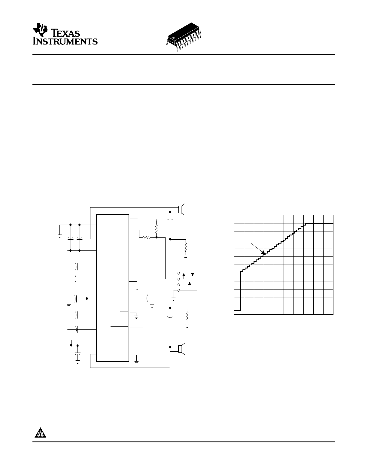
DC VOLUME CONTROL
Volume - dB
BTL Volume
PGND
ROUT-
PV
DD
RIN+
RIN-
V
DD
LIN-
LIN+
PV
DD
LOUT-
1
ROUT+
SE/BTL
VOLUME
AGND
NC
BYPASS
FADE
SHUTDOWN
LOUT+
PGND
2
3
4
5
6
7
8
9
10
11
12
14
15
16
17
13
18
19
20
C
i
V
DD
V
DD
Right Positive
Differential Input Signal
Left Negative
Differential Input Signal
Right Negative
Differential Input Signal
Left Positive
Differential Input Signal
C
i
C
C
i
i
Power Supply
Power Supply
V
DD
100 kW
100 kW
C
330 FOm
C
330 FOm
0.47 Fm
0.47 Fm
0.47 Fm
0.47 Fm
0.47 Fm
0.47 Fm
0.47 Fm
C
10 FSm
C
0.47 F
(BYP)
m
In From DAC
or
Potentiometer
(DC Voltage)
System
Control
Right
Speaker
Left
Speaker
Headphones
1 kW
1 kW
2-W STEREO AUDIO POWER AMPLIFIER
WITH ADVANCED DC VOLUME CONTROL
FEATURES DESCRIPTION
• 2 W Into 4- Ω Speakers With External Heatsink
• DC Volume Control With 2-dB
Steps from -40 dB to 20 dB
– Fade Mode
– -85-dB Mute Mode
• Differential Inputs
• 1-µA Shutdown Current (Typical)
• Headphone Mode
APPLICATIONS
• LCD Monitors
TPA6021A4
SLOS465 – JUNE 2005
The TPA6021A4 is a stereo audio power amplifier
that drives 2 W/channel of continuous RMS power
into a 4- Ω load when utilizing a heat sink. Advanced
dc volume control minimizes external components
and allows BTL (speaker) volume control and SE
(headphone) volume control.
The 20-pin DIP package allows for the use of a
heatsink which provides higher output power.
To ensure a smooth transition between active and
shutdown modes, a fade mode ramps the volume up
and down.
PRODUCTION DATA information is current as of publication date.
Products conform to specifications per the terms of the Texas
Instruments standard warranty. Production processing does not
necessarily include testing of all parameters.
Please be aware that an important notice concerning availability, standard warranty, and use in critical applications of Texas
Instruments semiconductor products and disclaimers thereto appears at the end of this data sheet.
Copyright © 2005, Texas Instruments Incorporated
www.ti.com
TPA6021A4
SLOS465 – JUNE 2005
These devices have limited built-in ESD protection. The leads should be shorted together or the device
placed in conductive foam during storage or handling to prevent electrostatic damage to the MOS gates.
AVAILABLE OPTIONS
T
A
–40 ° C to 85 ° C TPA6021A4N
ABSOLUTE MAXIMUM RATINGS
over operating free-air temperature range (unless otherwise noted)
V
SS
V
I
T
A
T
J
T
stg
(1) Stresses beyond those listed under "absolute maximum ratings" may cause permanent damage to the device. These are stress ratings
only, and functional operation of the device at these or any other conditions beyond those indicated under "recommended operating
conditions" is not implied. Exposure to absolute-maximum-rated conditions for extended periods may affect device reliability.
Supply voltage, VDD, PV
Input voltage, RIN+, RIN-, LIN+,LIN- –0.3 V to VDD+0.3 V
Continuous total power dissipation See Dissipation Rating Table
Operating free-air temperature range –40 ° C to 85 ° C
Operating junction temperature range –40 ° C to 150 ° C
Storage temperature range –65 ° C to 85 ° C
Lead temperature 1,6 mm (1/16 inch) from case for 10 seconds 260 ° C
DD
PACKAGE
20-PIN PDIP (N)
(1)
UNIT
–0.3 V to 6 V
DISSIPATION RATING TABLE
PACKAGE
N 1.8 W 14.5 mW/ ° C 1.16 W 0.94 W
(1) All characterization is done using an external heatsink with θSA= 25 ° C/W. The resulting derating factor
is 22.2 mW/ ° C.
TA= 25 ° C DERATING FACTOR TA= 70 ° C TA= 85 ° C
POWER RATING ABOVE TA= 25 ° C POWER RATING POWER RATING
(1)
2
www.ti.com
TPA6021A4
SLOS465 – JUNE 2005
RECOMMENDED OPERATING CONDITIONS
MIN MAX UNIT
V
SS
V
IH
V
IL
T
A
ELECTRICAL CHARACTERISTICS
TA= 25 ° C, V
| V
OO
PSRR Power supply rejection ratio V
| IIH| 1 µA
| IIL| V
I
DD
I
DD
I
DD(SD)
Supply voltage, VDD, PV
High-level input voltage
Low-level input voltage
DD
SE/ BTL, FADE 0.8 x V
SHUTDOWN 2 V
SE/ BTL, FADE 0.6 x V
SHUTDOWN 0.8 V
4 5.5 V
DD
Operating free-air temperature –40 85 ° C
= PV
DD
= 5.5 V (unless otherwise noted)
DD
PARAMETER TEST CONDITIONS MIN TYP MAX UNIT
V
= 5.5 V, Gain = 0 dB, SE/ BTL = 0 V 30 mV
| Output offset voltage (measured differentially)
High-level input current (SE/ BTL, FADE, SHUT- V
DOWN, VOLUME) VI= V
Low-level input current (SE/ BTL, FADE, SHUTDOWN, VOLUME)
Supply current, no load mA
Supply current, max power into a 4- Ω load SHUTDOWN = 2 V, RL= 4 Ω , 1.3 A
DD
V
= 5.5 V, Gain = 20 dB, SE/ BTL = 0 V 50 mV
DD
= PV
DD
DD
DD
V
DD
SHUTDOWN = 2 V
V
DD
SHUTDOWN = 2 V
V
DD
= 4 V to 5.5 V –42 –70 dB
DD
= PV
= 5.5 V,
DD
= PV
DD
DD
= PV
= 5.5 V, VI= 0 V 1 µA
DD
= PV
= 5.5 V, SE/ BTL = 0 V,
DD
= PV
= 5.5 V, SE/ BTL = 5.5 V,
DD
= 5 V = PV
, SE/ BTL = 0 V,
DD
6 7.5 9
3 5 6
PO= 2 W, stereo
Supply current, shutdown mode SHUTDOWN = 0 V 1 20 µA
DD
V
V
RMS
OPERATING CHARACTERISTICS
TA= 25 ° C, V
P
O
THD+N Total harmonic distortion + noise PO= 1 W, RL= 8 Ω , f = 20 Hz to 20 kHz <0.8%
V
OH
V
OL
V
(Bypass)
Z
I
(1) Requires an external heatsink with θSA≤ 25 ° C/W.
= PV
DD
= 5 V, RL= 4 Ω , Gain = 20 dB, Stereo, External Heatsink (unless otherwise noted)
DD
PARAMETER TEST CONDITIONS MIN TYP MAX UNIT
Output power W
High-level output voltage RL= 8 Ω , Measured between output and V
Low-level output voltage 400 mV
Bypass voltage (Nominally VDD/2) Measured at pin 16, No load, V
Supply ripple rejection ratio f = 1 kHz, Gain = 0 dB, C
Noise output voltage BTL 36 µV
THD = 1%, f = 1 kHz 1.5
THD = 10%, f = 1 kHz, V
= 5 V 2
DD
= 5.5 V 700 mV
DD
RL= 8 Ω , Measured between output and GND,
V
= 5.5 V
DD
= 5.5 V 2.65 2.75 2.85 V
DD
= 0.47 µF
(BYP)
BTL –82 dB
SE –57 dB
f = 20 Hz to 20 kHz, Gain = 0 dB,
C
= 0.47 µF
(BYP)
Input impedance (see Figure 18 ) VOLUME = 5 V 14 k Ω
(1)
(1)
RMS
3
www.ti.com
1
2
3
4
5
6
7
8
9
10
20
ROUT+PGND
19
SE/BTL
ROUT-
18
VOLUME
PVDD
17
AGND
RIN+
16
BYPASS
RIN-
15
FADE
VDD
14
SHUTDOWN
LIN-
13
NC
LIN+
12
LOUT+
PVDD
1
PGND
1
LOUT-
TPA6021A4
SLOS465 – JUNE 2005
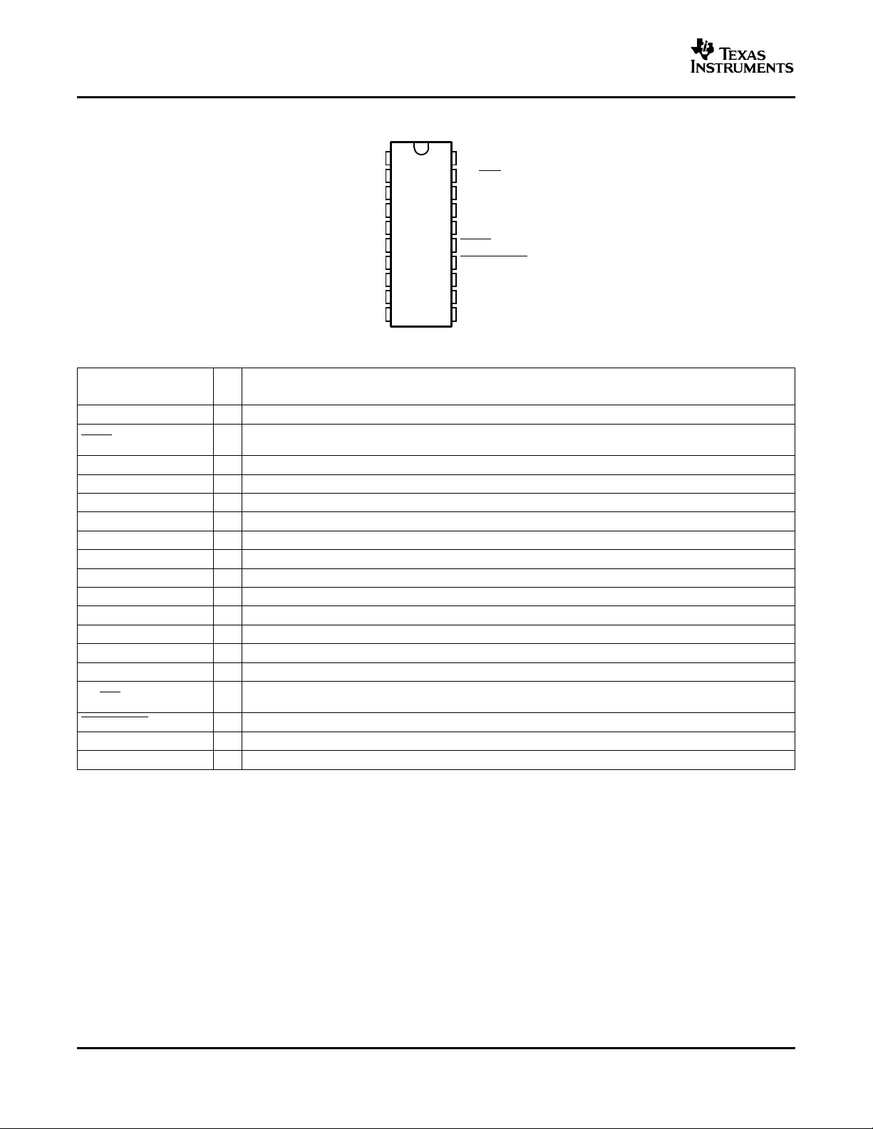
N (PDIP) PACKAGE
(TOP VIEW)
Terminal Functions
TERMINAL
NAME NO.
BYPASS 16 I Tap to voltage divider for internal midsupply bias generator used for analog reference
FADE 15 I
AGND 17 - Analog power supply ground
LIN- 7 I Left channel negative input for fully differential input.
LIN+ 8 I Left channel positive input for fully differential input.
LOUT– 10 O Left channel negative audio output
LOUT+ 12 O Left channel positive audio output.
NC 13 - No connection
PGND 1, 11 - Power ground
PVDD 3, 9 - Supply voltage terminal for power stage
RIN- 5 I Right channel negative input for fully differential input.
RIN+ 4 I Right channel positive input for fully differential input.
ROUT– 2 O Right channel negative audio output
ROUT+ 20 O Right channel positive audio output
SE/ BTL 19 I
SHUTDOWN 14 I Places the amplifier in shutdown mode if a TTL logic low is placed on this terminal
VDD 6 - Supply voltage terminal
VOLUME 18 I Terminal for dc volume control. DC voltage range is 0 to VDD.
I/O DESCRIPTION
Places the amplifier in fade mode if a logic low is placed on this terminal; normal operation if a logic high is
placed on this terminal.
Output control. When this terminal is high, SE outputs are selected. When this terminal is low, BTL outputs
are selected.
4
www.ti.com
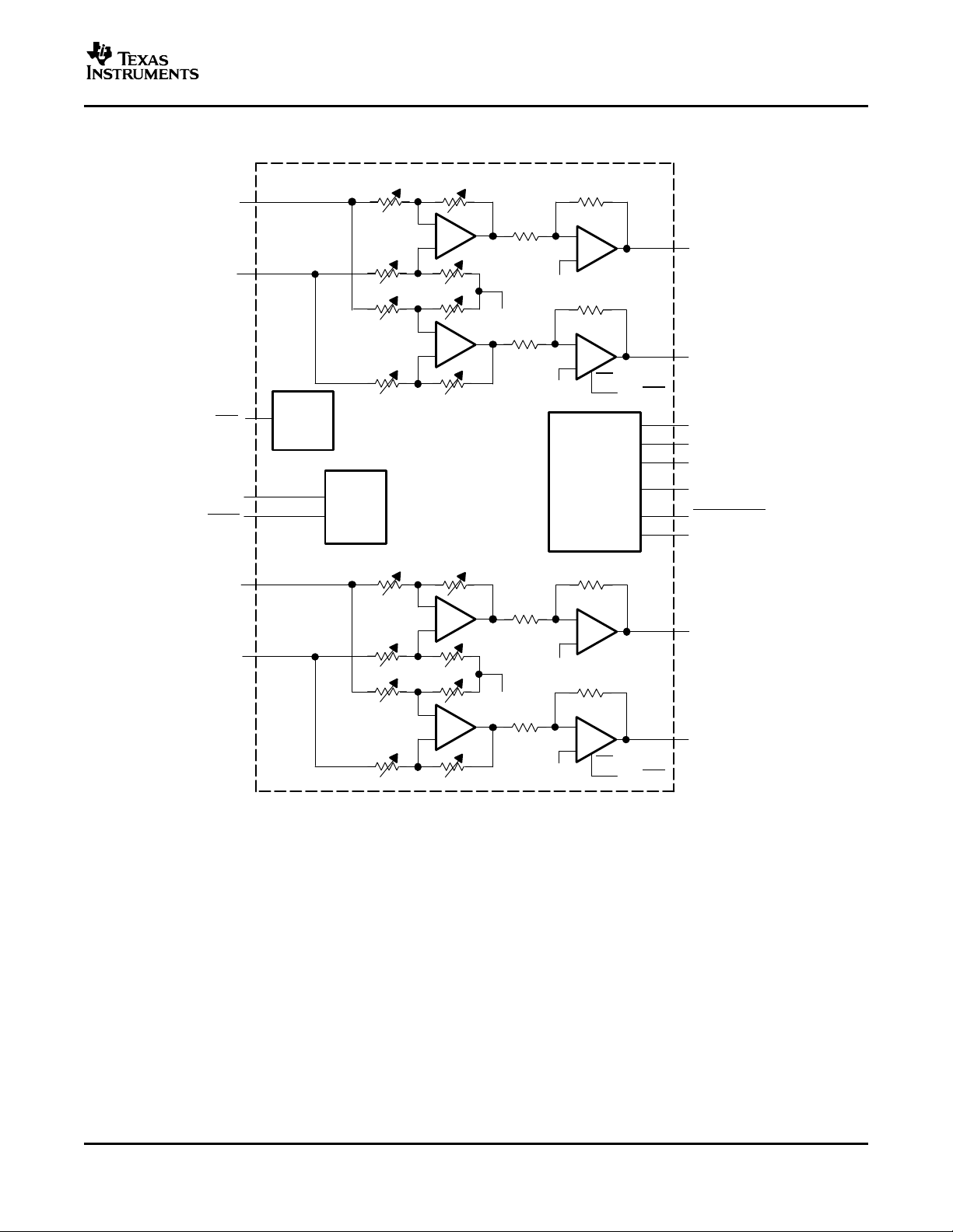
FUNCTIONAL BLOCK DIAGRAM
Power
Management
32-Step
Volume
Control
Output
Control
RIN+
ROUT+
SHUTDOWN
ROUT-
PV
DD
PGND
V
DD
BYPASS
AGND
LOUT-
LOUT+
RIN-
VOLUME
FADE
_
+
_
+
_
+
BYP
_
+
BYP
BYP
EN
SE/BTL
_
+
_
+
_
+
BYP
_
+
BYP
BYP
EN
SE/BTL
SE/BTL
LIN-
LIN+
TPA6021A4
SLOS465 – JUNE 2005
NOTE: All resistor wipers are adjusted with 32 step volume control.
5
www.ti.com
10
0.001
0.002
0.005
0.01
0.02
0.05
0.1
0.2
0.5
2
1
5
20 20 k50 100 200 500 1 k 2 k 5 k 10 k
P = 1.5 W
O
P = 0.25 W
O
f - Frequency - Hz
THD+N - Total Harmonic Distortion + Noise (BTL) - %
V = 5 V
R = 4
Gain = 20 dB
C = 0.47 F
BTL Stereo
DD
L
I
W
m
P = 1 W
O
10
0.001
0.002
0.005
0.01
0.02
0.05
0.1
0.2
0.5
2
1
5
20 20 k50 100 200 500 1 k 2 k 5 k 10 k
P = 0.25 W
O
P = 0.5 W
O
f - Frequency - Hz
THD+N - Total Harmonic Distortion + Noise (BTL) - %
V = 5 V
R = 8
Gain = 20 dB
C = 0.47 F
BTL Stereo
DD
L
I
W
m
P = 1 W
O
TPA6021A4
SLOS465 – JUNE 2005
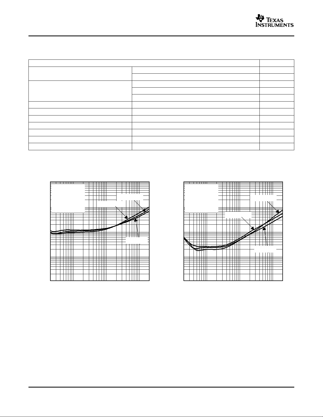
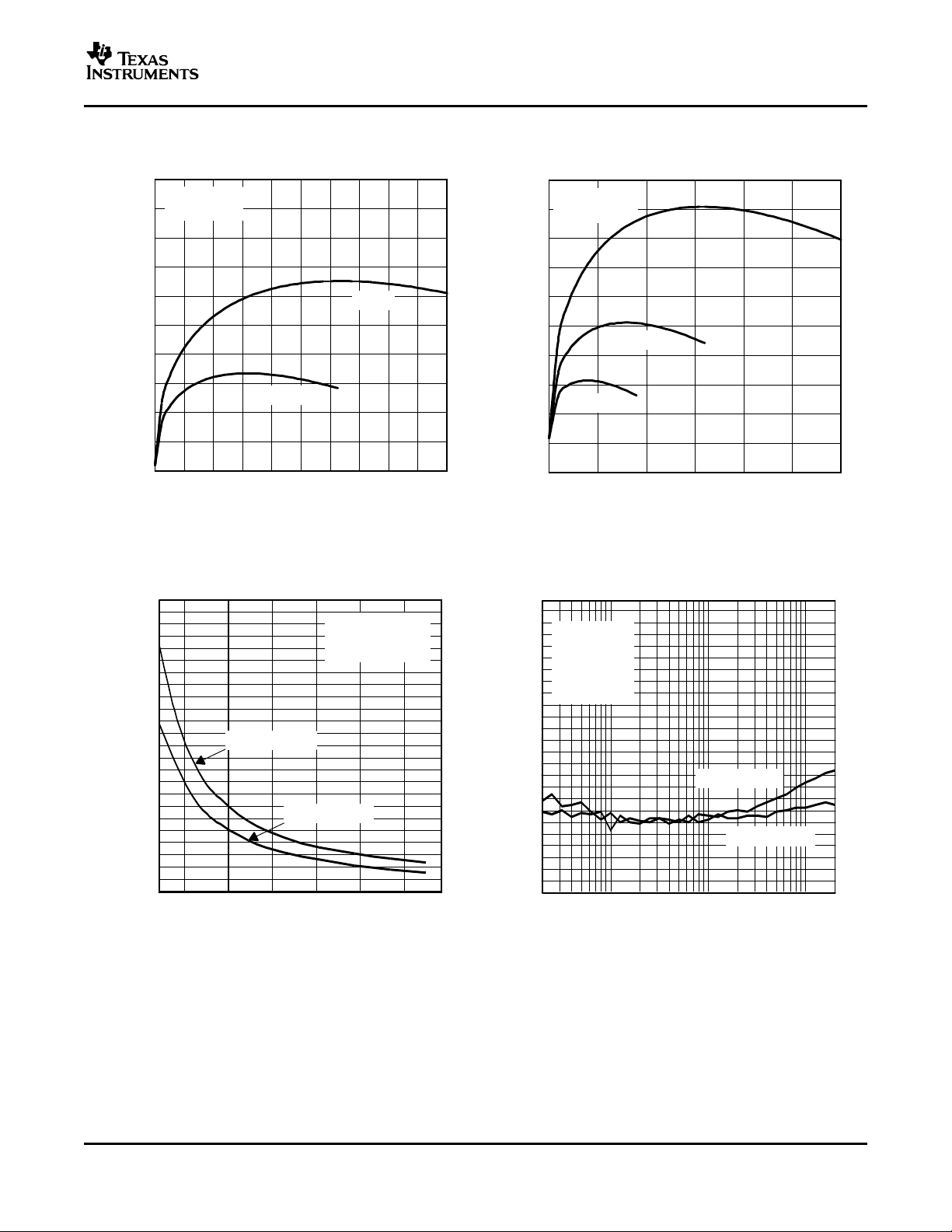
TYPICAL CHARACTERISTICS
Table of Graphs
THD+N Total harmonic distortion plus noise (BTL)
(1)
vs Frequency 1, 2
vs Output power 5, 6
vs Frequency 3, 4
THD+N Total harmonic distortion plus noise (SE) vs Output power 7
vs Output voltage 8
Closed loop response 9, 10
P
P
Power Dissipation vs Output power 11, 12
D
Output power vs Load resistance 13
O
Crosstalk vs Frequency 14, 15
PSRR Power supply ripple rejection (BTL) vs Frequency 16
PSRR Power supply ripple rejection (SE) vs Frequency 17
Z
Input impedance vs BTL gain 18
I
(1) All graphs were taken using an external heatsink with θSA= 25 ° C/W.
TOTAL HARMONIC DISTORTION + NOISE (BTL) TOTAL HARMONIC DISTORTION + NOISE (BTL)
vs vs
FREQUENCY FREQUENCY
FIGURE
6
Figure 1. Figure 2.
www.ti.com
10
0.01
0.02
0.05
0.1
0.2
0.5
1
2
5
20
20 k50 100 200 500 1 k 2 k 5 k 10 k
f - Frequency - Hz
THD+N - Total Harmonic Distortion + Noise (SE) - %
V = 5 V
R = 32
Gain = 14 dB
C = 0.47 F
SE Stereo
DD
L
I
W
m
C = 330 FOm
P = 75 WOm
10
0.01
0.02
0.05
0.1
0.2
0.5
1
2
5
20 20 k50 100 200 500 1 k 2 k 5 k 10 k
f - Frequency - Hz
THD+N - Total Harmonic Distortion + Noise (SE) - %
V = 1 V
O RMS
V = 5 V
R = 10 k
Gain = 14 dB
C = 0.47 F
SE Stereo
DD
L
I
W
m
C = 330 FOm
10
0.01
0.02
0.05
0.1
0.2
0.5
1
2
5
5
0.020.01 0.05 0.1 0.2 0.5
1 2
PO- Output Power - W
THD+N - Total Harmonic Distortion + Noise (BTL) - %
20 Hz
V = 5 V
R = 4
Gain = 20 dB
C = 0.47 F
BTL Stereo
DD
L
I
W
m
20 kHz
1 kHz
10
0.01
0.02
0.05
0.1
0.2
0.5
1
2
5
50.02
0.01
0.05 0.1 0.2 0.5 1 2
PO- Output Power - W
THD+N - Total Harmonic Distortion + Noise (BTL) - %
1 kHz
20 Hz
V = 5 V
R = 8
Gain = 20 dB
C = 0.47 F
BTL Stereo
DD
L
I
W
m
20 kHz
TPA6021A4
SLOS465 – JUNE 2005
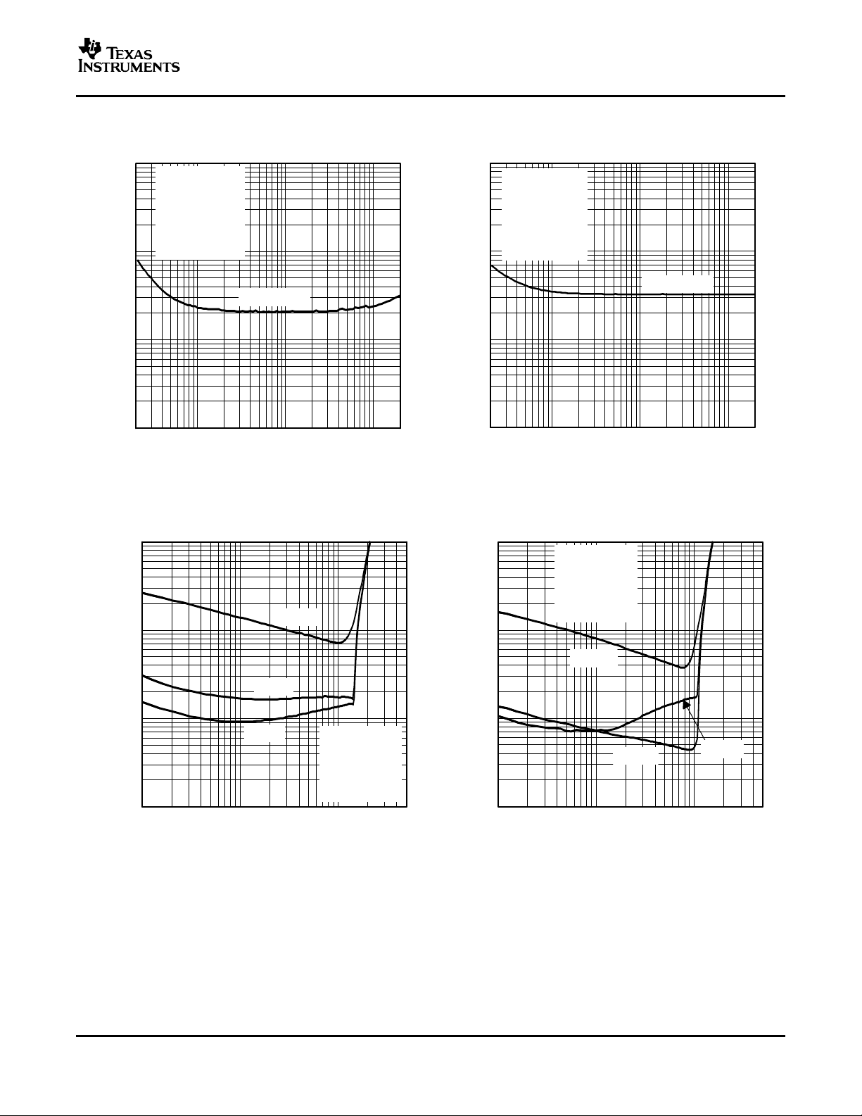
TOTAL HARMONIC DISTORTION + NOISE (SE) TOTAL HARMONIC DISTORTION + NOISE (SE)
vs vs
FREQUENCY FREQUENCY
Figure 3. Figure 4.
TOTAL HARMONIC DISTORTION + NOISE (BTL) TOTAL HARMONIC DISTORTION + NOISE (BTL)
vs vs
OUTPUT POWER OUTPUT POWER
Figure 5. Figure 6.
7
www.ti.com
10
0.01
0.02
0.05
0.1
0.2
0.5
1
2
5
10 20 30 40
200
50 100
P
O
- Output Power - mW
THD+N - Total Harmonic Distortion + Noise (SE) - %
V = 5 V
R = 32
Gain = 14 dB
C = 0.47 F
SE Stereo
DD
L
I
W
m
C = 330 FOm
20 Hz
1 kHz
20 kHz
10
0.001
0.002
0.005
0.01
0.02
0.05
0.1
0.2
0.5
1
2
5
0 0.2 0.60.4
0.8
1
1.2
1.6
1.4
1.8
2
THD+N - T otal Harmonic Distortion + Noise (SE) - %
20 kHz
20 Hz
V - Output Voltage - rms
O
V = 5 V
R = 10 k
Gain = 14 dB
C = 0.47 F
SE Stereo
DD
L
I
W
m
C = 330 FOm
1 kHz
150
120
90
60
30
0
-30
-80
-70
-60
-50
-40
-30
-20
-10
0
10
20
30
40
10 100 1 k 10 k 100 k 1 M
-180
-150
-120
-90
-60
180
Gain
Phase
V = 5 V
R = 8
Mode = BTL
Gain = 0 dB
DD
L
W
f - Frequency - Hz
Closed Loop Gain - dB
Phase - Degrees
150
120
90
60
30
0
-30
-80
-70
-60
-50
-40
-30
-20
-10
0
10
20
30
40
10 100 1 k 10 k 100 k 1 M
-180
-150
-120
-90
-60
180
Gain
Phase
f - Frequency - Hz
Closed Loop Gain - dB
Phase - Degrees
V = 5 V
R = 8
Mode = BTL
Gain = 20 dB
DD
L
W
TPA6021A4
SLOS465 – JUNE 2005
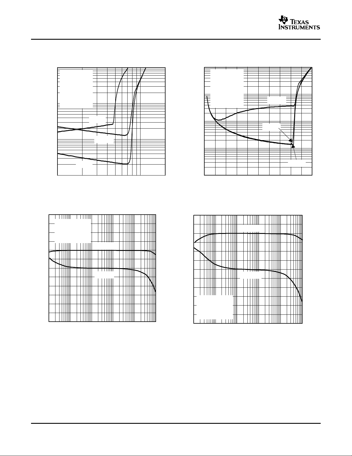
TOTAL HARMONIC DISTORTION + NOISE (SE) TOTAL HARMONIC DISTORTION + NOISE (SE)
vs vs
OUTPUT POWER OUTPUT VOLTAGE
Figure 7. Figure 8.
CLOSED LOOP RESPONSE CLOSED LOOP RESPONSE
Figure 9. Figure 10.
8
www.ti.com
0
0.2
0.4
0.6
0.8
1
1.2
1.4
1.6
1.8
2
0 0.2 0.4 0.6 0.8 1 1.2 1.4 1.6 1.8 2
PO- Output Power - W
4 W
8 W
V = 5 V
BTL
DD
P - Power Dissipation (Per Channel) - W
D
0
20
40
60
80
100
120
140
160
180
200
0 100 150 200 250 30050
8 W
16 W
32 W
P
O
- Output Power - mW
V = 5 V
SE
DD
P - Power Dissipation (Per Channel) - mW
D
0
0.5
1
1.5
4 10 20 30 40 50 60 70
R - Load Resistance -LW
P - Output Power - W
O
2
THD+N = 10%
THD+N = 1%
2.5
V = 5 V
Gain = 20 dB
BTL Stereo
DD
-140
-40
-120
-100
-80
-60
20 20 k100 200
1 k 2 k
10 k
f - Frequency - Hz
Crosstalk - dB
Left to Right
Right to Left
V = 5 V
P = 1 W
R = 8
Gain = 0 dB
BTL
DD
O
L
W
TPA6021A4
SLOS465 – JUNE 2005
POWER DISSIPATION (PER CHANNEL) POWER DISSIPATION (PER CHANNEL)
vs vs
OUTPUT POWER OUTPUT POWER
Figure 11. Figure 12.
OUTPUT POWER CROSSTALK
vs vs
LOAD RESISTANCE FREQUENCY
Figure 13. Figure 14.
9

www.ti.com
20 20 k100 1 k 10 k
f - Frequency - Hz
PSRR - Power Supply Rejection Ratio (SE) - dB
-100
0
-90
-80
-70
-60
-50
-40
-30
-20
-10
Gain = 0 dB
Gain = 20 dB
V = 5 V
R = 8
C = 0.47 F
BTL
DD
L
(BYP)
W
m
C = 0.47 FIm
-140
-40
-120
-100
-80
-60
20 20 k100 200
1 k 2 k
10 k
f - Frequency - Hz
Crosstalk - dB
Left to Right
Right to Left
V = 5 V
P = 1 W
R = 8
Gain = 20 dB
BTL
DD
O
L
W
20 20 k100 1 k 10 k
f - Frequency - Hz
PSRR - Power Supply Rejection Ratio (SE) - dB
-100
0
-90
-80
-70
-60
-50
-40
-30
-20
-10
Gain = 14 dB
Gain = 0 dB
V = 5 V
R = 32
C = 0.47 F
SE
DD
L
(BYP)
W
m
C = 0.47 F
C = 330 F
I
O
m
m
0
10
20
30
40
50
60
70
80
90
−40 −30 −20 −10
0
10 20
BTL Gain − dB
− Input Impedamce − Z
I
kΩ
TPA6021A4
SLOS465 – JUNE 2005
CROSSTALK POWER SUPPLY REJECTION RATIO (BTL)
vs vs
FREQUENCY FREQUENCY
Figure 15. Figure 16.
POWER SUPPLY REJECTION RATIO (SE) INPUT IMPEDANCE
FREQUENCY BTL GAIN
10
Figure 17. Figure 18.
vs vs

www.ti.com
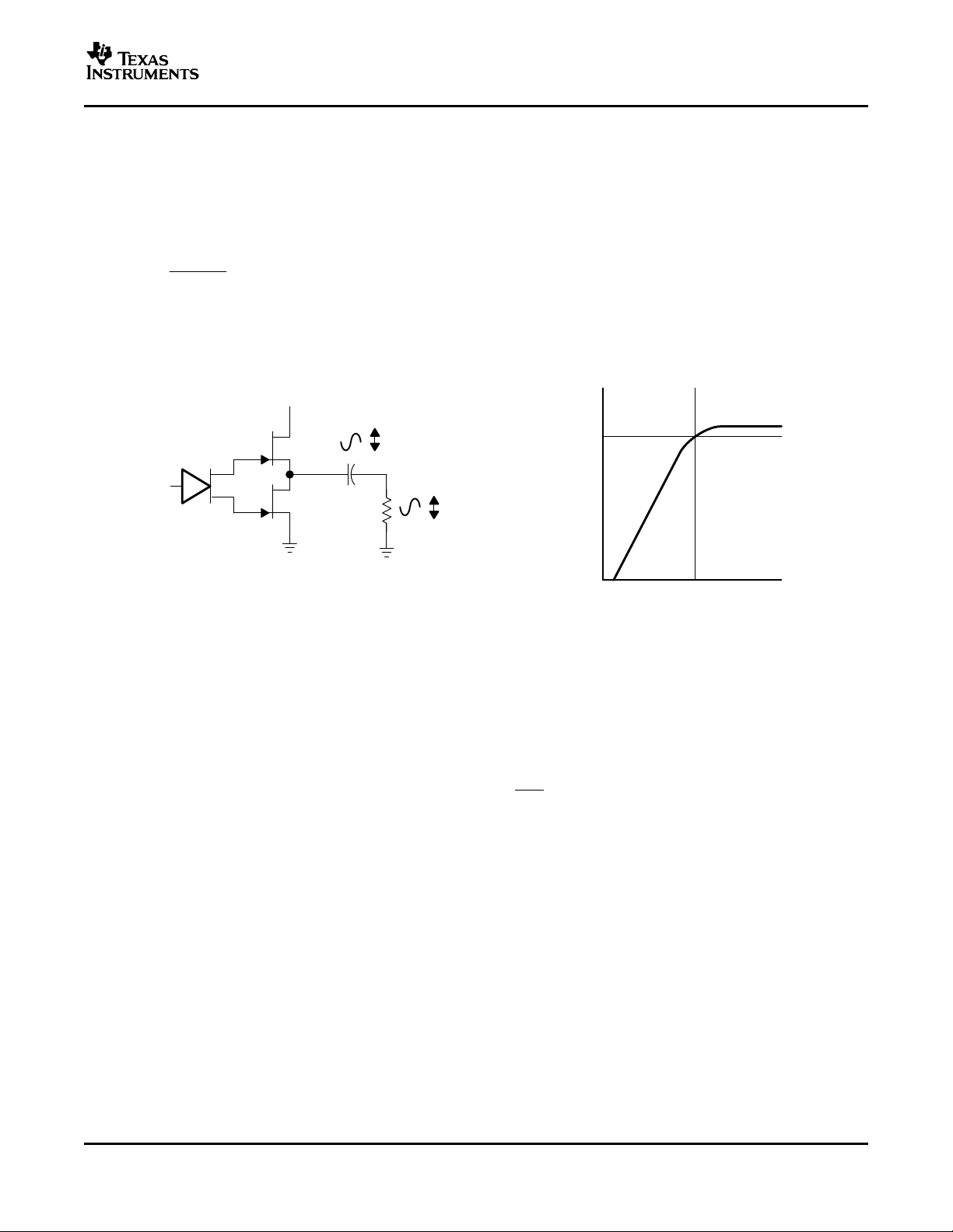
APPLICATION INFORMATION
PGND
ROUT-
PV
DD
RIN+
RIN-
V
DD
LIN-
LIN+
PV
DD
LOUT-
1
ROUT+
SE/BTL
VOLUME
AGND
NC
BYPASS
FADE
SHUTDOWN
LOUT+
PGND
2
3
4
5
6
7
8
9
10
11
12
14
15
16
17
13
18
19
20
C
i
Right
Audio Source
Left
Audio Source
C
i
C
i
C
i
Power Supply
Power Supply
V
DD
100 kW
100 kW
In From DAC
or
Potentiometer
(DC Voltage)
System
Control
Right
Speaker
Left
Speaker
Headphones
1 kW
1 kW
C
330 FOm
C
330 FOm
C
0.47 F
(BYP)
m
0.47 Fm
0.47 Fm
0.47 Fm
0.47 Fm
0.47 Fm
0.47 Fm
0.47 Fm
V
DD
V
DD
C
10 FSm
SELECTION OF COMPONENTS
Figure 19 and Figure 20 are schematic diagrams of typical LCD monitor application circuits.
TPA6021A4
SLOS465 – JUNE 2005
A. A 0.47-µF ceramic capacitor should be placed as close as possible to the IC. For filtering lower-frequency noise
signals, a larger electrolytic capacitor of 10 µF or greater should be placed near the audio power amplifier.
Figure 19. Typical TPA6021A4 Application Circuit Using Single-Ended Inputs and Input MUX
11

www.ti.com
PGND
ROUT-
PV
DD
RIN+
RIN-
V
DD
LIN-
LIN+
PV
DD
LOUT-
1
ROUT+
SE/BTL
VOLUME
AGND
NC
BYPASS
FADE
SHUTDOWN
LOUT+
PGND
2
3
4
5
6
7
8
9
10
11
12
14
15
16
17
13
18
19
20
C
i
V
DD
V
DD
Right Positive
Differential Input Signal
Left Negative
Differential Input Signal
Right Negative
Differential Input Signal
Left Positive
Differential Input Signal
C
i
C
C
i
i
Power Supply
Power Supply
V
DD
100 kW
100 kW
C
330 FOm
C
330 FOm
0.47 Fm
0.47 Fm
0.47 Fm
0.47 Fm
0.47 Fm
0.47 Fm
0.47 Fm
C
10 FSm
C
0.47 F
(BYP)
m
In From DAC
or
Potentiometer
(DC Voltage)
System
Control
Right
Speaker
Left
Speaker
Headphones
1 kW
1 kW
TPA6021A4
SLOS465 – JUNE 2005
APPLICATION INFORMATION (continued)
A. A 0.47-µF ceramic capacitor should be placed as close as possible to the IC. For filtering lower-frequency noise
SE/ BTL OPERATION
The ability of the TPA6021A4 to easily switch between BTL and SE modes is one of its most important cost
saving features. This feature eliminates the requirement for an additional headphone amplifier in applications
where internal stereo speakers are driven in BTL mode but external headphone or speakers must be
accommodated. Internal to the TPA6021A4, two separate amplifiers drive OUT+ and OUT–. The SE/ BTL input
controls the operation of the follower amplifier that drives LOUT– and ROUT–. When SE/ BTL is held low, the
amplifier is on and the TPA6021A4 is in the BTL mode. When SE/ BTL is held high, the OUT– amplifiers are in a
high output impedance state, which configures the TPA6021A4 as an SE driver from LOUT+ and ROUT+. IDDis
reduced by approximately one-third in SE mode. Control of the SE/ BTL input can be from a logic-level CMOS
source or, more typically, from a resistor divider network as shown in Figure 21 . The trip level for the SE/ BTL
input can be found in the recommended operating conditions table.
12
signals, a larger electrolytic capacitor of 10 µF or greater should be placed near the audio power amplifier.
Figure 20. Typical TPA6021A4 Application Circuit Using Differential Inputs

www.ti.com
SE/BTL
ROUT+ 20
RIN+
4
5 RIN-
ROUT- 2
1 kW
C
O
330 Fm
100 kW
19
100 kW
V
DD
_
+
_
+
Bypass
_
+
Bypass
EN
_
+
Bypass
LOUT+
APPLICATION INFORMATION (continued)
TPA6021A4
SLOS465 – JUNE 2005
Figure 21. TPA6021A4 Resistor Divider Network Circuit
Using a 1/8-in. (3,5 mm) stereo headphone jack, the control switch is closed when no plug is inserted. When
closed the 100-k Ω /1-k Ω divider pulls the SE/ BTL input low. When a plug is inserted, the 1-k Ω resistor is
disconnected and the SE/ BTL input is pulled high. When the input goes high, the OUT– amplifier is shut down
causing the speaker to mute (open-circuits the speaker). The OUT+ amplifier then drives through the output
capacitor (C
) into the headphone jack.
o
SHUTDOWN MODES
The TPA6021A4 employs a shutdown mode of operation designed to reduce supply current (I
minimum level during periods of nonuse for power conservation. The SHUTDOWN input terminal should be held
high during normal operation when the amplifier is in use. Pulling SHUTDOWN low causes the outputs to mute
and the amplifier to enter a low-current state, I
= 20 µA. SHUTDOWN should never be left unconnected
DD
because amplifier operation would be unpredictable.
Table 1. SE/ BTL and Shutdown Functions
(1)
INPUTS
SE/ BTL SHUTDOWN OUTPUT
X Low Mute
Low High BTL
High High SE
(1) Inputs should never be left unconnected.
FADE OPERATION
For design flexibility, a fade mode is provided to slowly ramp up the amplifier gain when coming out of shutdown
mode and conversely ramp the gain down when going into shutdown. This mode provides a smooth transition
between the active and shutdown states and virtually eliminates any pops or clicks on the outputs.
AMPLIFIER STATE
) to the absolute
DD
13

www.ti.com
ROUT+
Device Shutdown
ROUT+
Device Shutdown
TPA6021A4
SLOS465 – JUNE 2005
When the FADE input is a logic low, the device is placed into fade-on mode. A logic high on this pin places the
amplifier in the fade-off mode. The voltage trip levels for a logic low (V
recommended operating conditions table.
When a logic low is applied to the FADE pin and a logic low is then applied on the SHUTDOWN pin, the channel
gain steps down from gain step to gain step at a rate of two clock cycles per step. With a nominal internal clock
frequency of 58 Hz, this equates to 34 ms (1/29 Hz) per step. The gain steps down until the lowest gain step is
reached. The time it takes to reach this step depends on the gain setting prior to placing the device in shutdown.
For example, if the amplifier is in the highest gain mode of 20 dB, the time it takes to ramp down the channel
gain is 1.05 seconds. This number is calculated by taking the number of steps to reach the lowest gain from the
highest gain, or 31 steps, and multiplying by the time per step, or 34 ms.
After the channel gain is stepped down to the lowest gain, the amplifier begins discharging the bypass capacitor
from the nominal voltage of V
/2 to ground. This time is dependent on the value of the bypass capacitor. For a
DD
0.47-µF capacitor that is used in the application diagram in Figure 19 , the time is approximately 500 ms. This
time scales linearly with the value of bypass capacitor. For example, if a 1-µF capacitor is used for bypass, the
time period to discharge the capacitor to ground is twice that of the 0.47-µF capacitor, or 1 second. Figure 22
below is a waveform captured at the output during the shutdown sequence when the part is in fade-on mode.
The gain is set to the highest level and the output is at V
when the amplifier is shut down.
DD
When a logic high is placed on the SHUTDOWN pin and the FADE pin is still held low, the device begins the
start-up process. The bypass capacitor will begin charging. Once the bypass voltage reaches the final value of
V
/2, the gain increases in 2-dB steps from the lowest gain level to the gain level set by the dc voltage applied
DD
to the VOLUME pin.
In the fade-off mode, the output of the amplifier immediately drops to V
smooth discharge to ground. When shutdown is released, the bypass capacitor charges up to V
channel gain returns immediately to the value on the VOLUME terminal. Figure 23 below is a waveform captured
at the output during the shutdown sequence when the part is in the fade-off mode. The gain is set to the highest
level, and the output is at V
when the amplifier is shut down.
DD
The power-up sequence is different from the shutdown sequence and the voltage on the FADE pin does not
change the power-up sequence. Upon a power-up condition, the TPA6021A4 begins in the lowest gain setting
and steps up 2 dB every 2 clock cycles until the final value is reached as determined by the dc voltage applied to
the VOLUME pin.
) or logic high (V
IL
/2 and the bypass capacitor begins a
DD
) can be found in the
IH
DD
/2 and the
14
Figure 22. Shutdown Sequence in the Figure 23. Shutdown Sequence in the
Fade-on Mode Fade-off Mode

www.ti.com
-90
-80
-70
-60
-50
-40
-30
-20
-10
0
10
20
30
0 0.5 1 1.5 2 2.5 3 3.5 4 4.5 5
Volume [Pin 18] - V
Volume - dB
BTL Volume
TPA6021A4
SLOS465 – JUNE 2005
VOLUME OPERATION
The VOLUME pin controls the BTL volume when driving speakers, and the SE volume when driving
headphones. This pin is controlled with a dc voltage, which should not exceed V
The output volume increases in discrete steps as the dc voltage increases and decreases in discrete steps as
the dc voltage decreases. There are a total of 32 discrete gain steps of the amplifier and range from -85 dB to 20
dB for BTL operation and -85 dB to 14 dB for SE operation.
A pictorial representation of the typical volume control can be found in Figure 24 .
.
DD
Figure 24. Typical DC Volume Control Operation
15

www.ti.com
C
IN
R
i
R
f
Input Signal
ƒ
3 dB
1
2 CR
i
f
c(highpass)
1
2 RiC
i
−3 dB
f
c
C
i
1
2 Rif
c
TPA6021A4
SLOS465 – JUNE 2005
INPUT RESISTANCE
Each gain setting is achieved by varying the input resistance of the amplifier, which can range from its smallest
value to over six times that value. As a result, if a single capacitor is used in the input high-pass filter, the –3 dB
or cutoff frequency also changes by over six times.
Figure 25. Resistor on Input for Cut-Off Frequency
The input resistance at each gain setting is given in Figure 18 .
The –3-dB frequency can be calculated using Equation 1 .
(1)
INPUT CAPACITOR, C
In the typical application an input capacitor (C
proper dc level for optimum operation. In this case, C
I
) is required to allow the amplifier to bias the input signal to the
I
and the input impedance of the amplifier (R
I
) form a
I
high-pass filter with the corner frequency determined in Equation 2 .
The value of CIis important to consider as it directly affects the bass (low frequency) performance of the circuit.
Consider the example where R
is 70 k Ω and the specification calls for a flat-bass response down to 40 Hz.
I
Equation 2 is reconfigured as Equation 3 .
In this example, C
consideration for this capacitor is the leakage path from the input source through the input network (C
is 56.8 nF, so one would likely choose a value in the range of 56 nF to 1 µF. A further
I
) and the
I
feedback network to the load. This leakage current creates a dc offset voltage at the input to the amplifier that
reduces useful headroom, especially in high gain applications. For this reason, a low-leakage tantalum or
ceramic capacitor is the best choice. When polarized capacitors are used, the positive side of the capacitor
should face the amplifier input in most applications as the dc level there is held at V
/2, which is likely higher
DD
than the source dc level. Note that it is important to confirm the capacitor polarity in the application.
(2)
(3)
16

www.ti.com
f
c(high)
1
2 RLC
(C)
−3 dB
f
c
TPA6021A4
SLOS465 – JUNE 2005
POWER SUPPLY DECOUPLING, C
(S)
The TPA6021A4 is a high-performance CMOS audio amplifier that requires adequate power supply decoupling to
ensure the output total harmonic distortion (THD) is as low as possible. Power supply decoupling also prevents
oscillations for long lead lengths between the amplifier and the speaker. The optimum decoupling is achieved by
using two capacitors of different types that target different types of noise on the power supply leads. For higher
frequency transients, spikes, or digital hash on the line, a good low equivalent-series-resistance (ESR) ceramic
capacitor, typically 0.1 µF placed as close as possible to the device V
lead, works best. For filtering
DD
lower-frequency noise signals, a larger aluminum electrolytic capacitor of 10 µF or greater placed near the audio
power amplifier is recommended.
MIDRAIL BYPASS CAPACITOR, C
The midrail bypass capacitor (C
start-up or recovery from shutdown mode, C
(BYP)
(BYP)
) is the most critical capacitor and serves several important functions. During
determines the rate at which the amplifier starts up. The second
(BYP)
function is to reduce noise produced by the power supply caused by coupling into the output drive signal. This
noise is from the midrail generation circuit internal to the amplifier, which appears as degraded PSRR and
THD+N.
Bypass capacitor (C
for the best THD and noise performance. For the best pop performance, choose a value for C
) values of 0.47-µF to 1-µF ceramic or tantalum low-ESR capacitors are recommended
(BYP)
(BYP)
that is equal to
or greater than the value chosen for CI. This ensures that the input capacitors are charged up to the midrail
voltage before C
OUTPUT COUPLING CAPACITOR, C
In the typical single-supply SE configuration, an output coupling capacitor (C
is fully charged to the midrail voltage.
(BYP)
(C)
) is required to block the dc bias at
(C)
the output of the amplifier, thus preventing dc currents in the load. As with the input coupling capacitor, the
output coupling capacitor and impedance of the load form a high-pass filter governed by Equation 4 .
The main disadvantage, from a performance standpoint, is the load impedances are typically small, which drives
the low-frequency corner higher, degrading the bass response. Large values of C
frequencies into the load. Consider the example where a C
of 330 µF is chosen and loads vary from 4 Ω , 8 Ω ,
(C)
are required to pass low
(C)
32 Ω , 10 k Ω , and 47 k Ω . Table 2 summarizes the frequency response characteristics of each configuration.
Table 2. Common Load Impedances vs Low Frequency
Output Characteristics in SE Mode
R
L
4 Ω 330 µF 120 Hz
8 Ω 330 µF 60 Hz
32 Ω 330 µF 15 Hz
10,000 Ω 330 µF 0.05 Hz
47,000 Ω 330 µF 0.01 Hz
C
(C)
LOWEST
FREQUENCY
(4)
17

www.ti.com
Power
V
(rms)
2
R
L
V
(rms)
V
O(PP)
2 2
R
L
2x V
O(PP)
V
O(PP)
-V
O(PP)
V
DD
V
DD
TPA6021A4
SLOS465 – JUNE 2005
As Table 2 indicates, most of the bass response is attenuated into a 4- Ω load, an 8- Ω load is adequate,
headphone response is good, and drive into line level inputs (a home stereo for example) is exceptional.
USING LOW-ESR CAPACITORS
Low-ESR capacitors are recommended throughout this applications section. A real (as opposed to ideal)
capacitor can be modeled simply as a resistor in series with an ideal capacitor. The voltage drop across this
resistor minimizes the beneficial effects of the capacitor in the circuit. The lower the equivalent value of this
resistance, the more the real capacitor behaves like an ideal capacitor.
BRIDGE-TIED LOAD vs SINGLE-ENDED LOAD
Figure 26 shows a Class-AB audio power amplifier (APA) in a BTL configuration. The TPA6021A4 BTL amplifier
consists of two Class-AB amplifiers driving both ends of the load. There are several potential benefits to this
differential drive configuration, but, initially consider power to the load. The differential drive to the speaker
means that as one side is slewing up, the other side is slewing down, and vice versa. This in effect doubles the
voltage swing on the load as compared to a ground referenced load. Plugging 2 x V
where voltage is squared, yields 4x the output power from the same supply rail and load impedance (see
Equation 5 ).
into the power equation,
O(PP)
(5)
Figure 26. Bridge-Tied Load Configuration
18
www.ti.com
f
(c)
1
2 R
LCC
R
L
C
(C)
V
O(PP)
V
O(PP)
V
DD
-3 dB
f
c
TPA6021A4
SLOS465 – JUNE 2005
In a typical computer sound channel operating at 5 V, bridging raises the power into an 8- Ω speaker from a
singled-ended (SE, ground reference) limit of 250 mW to 1 W. In sound power that is a 6-dB improvement, which
is loudness that can be heard. In addition to increased power there are frequency response concerns. Consider
the single-supply SE configuration shown in Figure 27 . A coupling capacitor is required to block the dc offset
voltage from reaching the load. These capacitors can be quite large (approximately 33 µF to 1000 µF), so they
tend to be expensive, heavy, occupy valuable PCB area, and have the additional drawback of limiting
low-frequency performance of the system. This frequency limiting effect is due to the high-pass filter network
created with the speaker impedance and the coupling capacitance and is calculated with Equation 6 .
For example, a 68-µF capacitor with an 8- Ω speaker would attenuate low frequencies below 293 Hz. The BTL
configuration cancels the dc offsets, which eliminates the need for the blocking capacitors. Low-frequency
performance is then limited only by the input network and speaker response. Cost and PCB space are also
minimized by eliminating the bulky coupling capacitor.
(6)
Figure 27. Single-Ended Configuration and Frequency Response
Increasing power to the load does carry a penalty of increased internal power dissipation. The increased
dissipation is understandable considering that the BTL configuration produces 4x the output power of the SE
configuration. Internal dissipation versus output power is discussed further in the crest factor and thermal
considerations section.
SINGLE-ENDED OPERATION
In SE mode (see Figure 27 ), the load is driven from the primary amplifier output for each channel (OUT+).
The amplifier switches single-ended operation when the SE/ BTL terminal is held high. This puts the negative
outputs in a high-impedance state, and effectively reduces the amplifier's gain by 6 dB.
BTL AMPLIFIER EFFICIENCY
Class-AB amplifiers are inefficient. The primary cause of these inefficiencies is voltage drop across the output
stage transistors. There are two components of the internal voltage drop. One is the headroom or dc voltage
drop that varies inversely to output power. The second component is due to the sinewave nature of the output.
The total voltage drop can be calculated by subtracting the RMS value of the output voltage from V
internal voltage drop multiplied by the RMS value of the supply current (I
rms) determines the internal power
DD
dissipation of the amplifier.
An easy-to-use equation to calculate efficiency starts out as being equal to the ratio of power from the power
supply to the power delivered to the load. To accurately calculate the RMS and average values of power in the
load and in the amplifier, the current and voltage waveform shapes must first be understood (see Figure 28 ).
DD
. The
19
www.ti.com
V
(LRMS)
V
O
I
DD
I
DD(avg)
Efficiency of a BTL amplifier
P
L
P
SUP
Where:
P
L
VLrms
2
R
L
, andV
LRMS
V
P
2
, therefore, P
L
V
P
2
2R
L
and
P
SUP
VDDIDDavg
and
IDDavg
1
0
V
P
R
L
sin(t) dt
1
V
P
R
L
[cos(t)]
0
2V
P
R
L
Therefore,
P
SUP
2 VDDV
P
R
L
Efficiency of a BTL amplifier
V
P
2
2 R
L
2 VDDV
P
R
L
V
P
4 V
DD
PL = Power delivered to load
P
SUP
= Power drawn from power supply
V
LRMS
= RMS voltage on BTL load
R
L
= Load resistance
VP 2 PLR
L
BTL
2 PLR
L
4 V
DD
Where:
Therefore,
VP = Peak voltage on BTL load
IDDavg = Average current drawn from the power supply
VDD = Power supply voltage
η
BTL
= Efficiency of a BTL amplifier
TPA6021A4
SLOS465 – JUNE 2005
Figure 28. Voltage and Current Waveforms for BTL Amplifiers
Although the voltages and currents for SE and BTL are sinusoidal in the load, currents from the supply are very
different between SE and BTL configurations. In an SE application the current waveform is a half-wave rectified
shape, whereas in BTL it is a full-wave rectified waveform. This means RMS conversion factors are different.
Keep in mind that for most of the waveform both the push and pull transistors are not on at the same time, which
supports the fact that each amplifier in the BTL device only draws current from the supply for half the waveform.
The following equations are the basis for calculating amplifier efficiency.
substituting PL and PSUP into Equation 7 ,
Table 3 employs Equation 8 to calculate efficiencies for four different output power levels. Note that the efficiency
of the amplifier is quite low for lower power levels and rises sharply as power to the load is increased resulting in
a nearly flat internal power dissipation over the normal operating range. Note that the internal dissipation at full
output power is less than in the half power range. Calculating the efficiency for a specific system is the key to
proper power supply design. For a stereo 1-W audio system with 8- Ω loads and a 5-V supply, we get an
efficiency of 0.628. Total output power is 2-W. Thus the maximum draw on the power supply is almost 3.25 W.
20
(7)
(8)

www.ti.com
P = 10Log
dB
= 10Log
P
W
P
ref
3 W
1 W
= 5 dB
P = 10 x P
W ref
PdB/10
TPA6021A4
SLOS465 – JUNE 2005
Table 3. Efficiency vs Output Power in 5-V, 8- Ω BTL Systems
OUTPUT POWER EFFICIENCY PEAK VOLTAGE INTERNAL DISSIPATION
(W) (%) (V) (W)
0.25 31.4 2.00 0.55
0.50 44.4 2.83 0.62
1.00 62.8 4.00 0.59
1.25 70.2 4.47
(1) High peak voltages cause the THD to increase.
A final point to remember about Class-AB amplifiers (either SE or BTL) is how to manipulate the terms in the
efficiency equation to utmost advantage when possible. Note that in equation 8, V
indicates that as V
goes down, efficiency goes up.
DD
CREST FACTOR AND THERMAL CONSIDERATIONS
Class-AB power amplifiers dissipate a significant amount of heat in the package under normal operating
conditions. A typical music CD requires 12 dB to 15 dB of dynamic range, or headroom above the average power
output, to pass the loudest portions of the signal without distortion. In other words, music typically has a crest
factor between 12 dB and 15 dB. When determining the optimal ambient operating temperature, the internal
dissipated power at the average output power level must be used. From the data sheet graph (Figure 5.), one
can see that when the TPA6021A4 is operating from a 5-V supply into a 4- Ω speaker at 1% THD, that output
power is 1.5-W so maximum instantaneous output power is 3-W. Use equation 9 to convert watts to dB.
(1)
0.53
is in the denominator. This
DD
Subtracting the headroom restriction to obtain the average listening level without distortion yields:
5 dB - 15 dB = –10 dB (15-dB crest factor)
5 dB - 12 dB = –7 dB (12-dB crest factor)
5 dB - 9 dB = –4 dB (9-dB crest factor)
5 dB - 6 dB = -1 dB (6-dB crest factor)
5 dB - 3 dB = 2 dB (3-dB crest factor)
To convert dB back into watts use equation 10.
= 48 mW (18-dB crest factor)
= 95 mW (15-dB crest factor)
= 190 mW (12-dB crest factor)
= 380 mW (9-dB crest factor)
= 750 mW (6-dB crest factor)
= 1500 mW (3-dB crest factor)
This is valuable information to consider when attempting to estimate the heat dissipation requirements for the
amplifier system. Comparing the worst case, which is 1.5 W of continuous power output with a 3-dB crest factor,
against 12-dB and 15-dB applications significantly affects maximum ambient temperature ratings for the system.
Using the power dissipation curves for a 5-V, 4- Ω system, the internal dissipation in the TPA6021A4 and
maximum ambient temperatures is shown in Table 4 .
(9)
(10)
21
www.ti.com
P
D(max)
2V
2
DD
2
R
L
q
JA
=
=
= 45 C/W
o
1
1
Derating Factor
0.0222
T
A
Max = T P
J JA D
Max - q
= 150 - 45 (0.6 x 2) = 96 C(15-dB crest factor)
o
TPA6021A4
SLOS465 – JUNE 2005
Table 4. TPA6021A4 Power Rating, 5-V, 4- Ω Stereo
PEAK OUTPUT POWER POWER DISSIPATION MAXIMUM AMBIENT
(W) (W/Channel) TEMPERATURE
3 1500 mW (3 dB) 1.26 37 ° C
3 750 mW (6 dB) 1.20 42 ° C
3 380 mW (9 dB) 1.00 59 ° C
3 190 mW (12 dB) 0.79 79 ° C
3 95 mW (15 dB) 0.60 96 ° C
3 48 mW (18 dB) 0.44 110 ° C
(1) Package limited to 85 ° C ambient.
PEAK OUTPUT POWER POWER DISSIPATION MAXIMUM AMBIENT
(W) (W/Channel) TEMPERATURE
2.2 1100 mW (3-dB crest factor) 0.57 99 ° C
2.2 876 mW (4-dB crest factor) 0.61 95 ° C
2.2 440 mW (7-dB crest factor) 0.62 95 ° C
2.2 220 mW (10-dB crest factor) 0.53 103 ° C
(1) Package limited to 85 ° C ambient.
The maximum dissipated power (P
a 4- Ω load. As a result, this simple formula for calculating P
AVERAGE OUTPUT POWER
Table 5. TPA6021A4 Power Rating, 5-V, 8- Ω Stereo
AVERAGE OUTPUT POWER
) is reached at a much lower output power level for an 8- Ω load than for
D(max)
D(max)
may be used for an 8- Ω application.
(1)
(1)
(1)
(1)
(1)
(1)
However, in the case of a 4- Ω load, the P
The amplifier may therefore be operated at a higher ambient temperature than required by the P
occurs at a point well above the normal operating power level.
D(max)
formula for
D(max)
a 4- Ω load.
The maximum ambient temperature depends on the heat-sinking ability of the PCB system. The derating factor
for the N package with an external heatsink is shown in the dissipation rating table. Use Equation 12 to convert
this to θ
.
JA.
To calculate maximum ambient temperatures, first consider that the numbers from the dissipation graphs are per
channel, so the dissipated power needs to be doubled for two channel operation. Given θJA, the maximum
allowable junction temperature, and the total internal dissipation, the maximum ambient temperature can be
calculated using Equation 13 . The maximum recommended junction temperature for the TPA6021A4 is 150 ° C.
The internal dissipation figures are taken from the Power Dissipation vs Output Power graphs.
NOTE:
Internal dissipation of 0.6 W is estimated for a 2-W system with 15-dB crest factor per
channel.
Table 4 and Table 5 show that some applications require no airflow to keep junction temperatures in the
specified range. The TPA6021A4 is designed with thermal protection that turns the device off when the junction
temperature surpasses 150 ° C to prevent damage to the IC. Table 4 and Table 5 were calculated for maximum
listening volume without distortion. When the output level is reduced the numbers in the table change
significantly. Also, using 8- Ω speakers increases the thermal performance by increasing amplifier efficiency.
(11)
(12)
(13)
22

PACKAGE OPTION ADDENDUM
www.ti.com
12-Aug-2005
PACKAGING INFORMATION
Orderable Device Status
(1)
Package
Type
Package
Drawing
Pins Package
Qty
Eco Plan
TPA6021A4N ACTIVE PDIP N 20 20 Pb-Free
(1)
The marketing statusvalues are defined as follows:
ACTIVE: Product devicerecommended for new designs.
LIFEBUY: TI hasannounced that the device willbe discontinued, and a lifetime-buy period is in effect.
NRND: Not recommended for new designs. Device is in production to support existing customers, but TI does not recommend using this part in
a new design.
PREVIEW: Device has been announced but is not in production. Samples may or may not be available.
OBSOLETE: TI has discontinued the production of the device.
(2)
Eco Plan - The planned eco-friendly classification: Pb-Free (RoHS) or Green (RoHS & no Sb/Br) - please check
http://www.ti.com/productcontent for the latest availability information and additional product content details.
TBD: The Pb-Free/Green conversion plan has not been defined.
Pb-Free (RoHS): TI's terms "Lead-Free" or "Pb-Free" mean semiconductor products that are compatible with the current RoHS requirements
for all 6 substances, including the requirement that lead not exceed 0.1% by weight in homogeneous materials. Where designed to be soldered
at high temperatures, TI Pb-Free products are suitable for use in specified lead-free processes.
Green (RoHS & no Sb/Br): TI defines "Green" to mean Pb-Free (RoHS compatible), and free of Bromine (Br) and Antimony (Sb) based flame
retardants (Br or Sb do not exceed 0.1% by weight in homogeneous material)
(3)
MSL, Peak Temp. -- The Moisture Sensitivity Level rating according to the JEDEC industry standard classifications, and peak solder
temperature.
(RoHS)
(2)
Lead/Ball Finish MSL Peak Temp
CU NIPDAU Level-NC-NC-NC
(3)
Important Information and Disclaimer:The information provided on this page represents TI's knowledge and belief as of the date that it is
provided. TI bases its knowledge and belief on information provided by third parties, and makes no representation or warranty as to the
accuracy of such information. Efforts are underway to better integrate information from third parties. TI has taken and continues to take
reasonable steps to provide representative and accurate information but may not have conducted destructive testing or chemical analysis on
incoming materials and chemicals. TI and TI suppliers consider certain information to be proprietary, and thus CAS numbers and other limited
information may not be available for release.
In no event shall TI's liability arising out of such information exceed the total purchase price of the TI part(s) at issue in this document sold by TI
to Customer on an annual basis.
Addendum-Page 1

PACKAGE OPTION ADDENDUM
www.ti.com
18-Jul-2006
PACKAGING INFORMATION
Orderable Device Status
(1)
Package
Type
Package
Drawing
Pins Package
Qty
Eco Plan
TPA6021A4N ACTIVE PDIP N 20 20 Pb-Free
TPA6021A4NE4 ACTIVE PDIP N 20 20 Pb-Free
(1)
The marketing status values are defined as follows:
ACTIVE: Product device recommended for new designs.
LIFEBUY: TI has announced that the device will be discontinued, and a lifetime-buy period is in effect.
NRND: Not recommended for new designs. Device is in production to support existing customers, but TI does not recommend using this part in
a new design.
PREVIEW: Device has been announced but is not in production. Samples may or may not be available.
OBSOLETE: TI has discontinued the production of the device.
(2)
Eco Plan - The planned eco-friendly classification: Pb-Free (RoHS), Pb-Free (RoHS Exempt), or Green (RoHS & no Sb/Br) - please check
http://www.ti.com/productcontent for the latest availability information and additional product content details.
TBD: The Pb-Free/Green conversion plan has not been defined.
Pb-Free (RoHS): TI's terms "Lead-Free" or "Pb-Free" mean semiconductor products that are compatible with the current RoHS requirements
for all 6 substances, including the requirement that lead not exceed 0.1% by weight in homogeneous materials. Where designed to be soldered
at high temperatures, TI Pb-Free products are suitable for use in specified lead-free processes.
Pb-Free (RoHS Exempt): This component has a RoHS exemption for either 1) lead-based flip-chip solder bumps used between the die and
package, or 2) lead-based die adhesive used between the die and leadframe. The component is otherwise considered Pb-Free (RoHS
compatible) as defined above.
Green (RoHS & no Sb/Br): TI defines "Green" to mean Pb-Free (RoHS compatible), and free of Bromine (Br) and Antimony (Sb) based flame
retardants (Br or Sb do not exceed 0.1% by weight in homogeneous material)
(RoHS)
(RoHS)
(2)
Lead/Ball Finish MSL Peak Temp
CU NIPDAU N / A for Pkg Type
CU NIPDAU N / A for Pkg Type
(3)
(3)
MSL, Peak Temp. -- The Moisture Sensitivity Level rating according to the JEDEC industry standard classifications, and peak solder
temperature.
Important Information and Disclaimer:The information provided on this page represents TI's knowledge and belief as of the date that it is
provided. TI bases its knowledge and belief on information provided by third parties, and makes no representation or warranty as to the
accuracy of such information. Efforts are underway to better integrate information from third parties. TI has taken and continues to take
reasonable steps to provide representative and accurate information but may not have conducted destructive testing or chemical analysis on
incoming materials and chemicals. TI and TI suppliers consider certain information to be proprietary, and thus CAS numbers and other limited
information may not be available for release.
In no event shall TI's liability arising out of such information exceed the total purchase price of the TI part(s) at issue in this document sold by TI
to Customer on an annual basis.
Addendum-Page 1

IMPORTANT NOTICE
Texas Instruments Incorporated and its subsidiaries (TI) reserve the right to make corrections, modifications,
enhancements, improvements, and other changes to its products and services at any time and to discontinue
any product or service without notice. Customers should obtain the latest relevant information before placing
orders and should verify that such information is current and complete. All products are sold subject to TI’s terms
and conditions of sale supplied at the time of order acknowledgment.
TI warrants performance of its hardware products to the specifications applicable at the time of sale in
accordance with TI’s standard warranty. Testing and other quality control techniques are used to the extent TI
deems necessary to support this warranty . Except where mandated by government requirements, testing of all
parameters of each product is not necessarily performed.
TI assumes no liability for applications assistance or customer product design. Customers are responsible for
their products and applications using TI components. To minimize the risks associated with customer products
and applications, customers should provide adequate design and operating safeguards.
TI does not warrant or represent that any license, either express or implied, is granted under any TI patent right,
copyright, mask work right, or other TI intellectual property right relating to any combination, machine, or process
in which TI products or services are used. Information published by TI regarding third-party products or services
does not constitute a license from TI to use such products or services or a warranty or endorsement thereof.
Use of such information may require a license from a third party under the patents or other intellectual property
of the third party, or a license from TI under the patents or other intellectual property of TI.
Reproduction of information in TI data books or data sheets is permissible only if reproduction is without
alteration and is accompanied by all associated warranties, conditions, limitations, and notices. Reproduction
of this information with alteration is an unfair and deceptive business practice. TI is not responsible or liable for
such altered documentation.
Resale of TI products or services with statements different from or beyond the parameters stated by TI for that
product or service voids all express and any implied warranties for the associated TI product or service and
is an unfair and deceptive business practice. TI is not responsible or liable for any such statements.
Following are URLs where you can obtain information on other Texas Instruments products and application
solutions:
Products Applications
Amplifiers amplifier.ti.com Audio www.ti.com/audio
Data Converters dataconverter.ti.com Automotive www.ti.com/automotive
DSP dsp.ti.com Broadband www.ti.com/broadband
Interface interface.ti.com Digital Control www.ti.com/digitalcontrol
Logic logic.ti.com Military www.ti.com/military
Power Mgmt power.ti.com Optical Networking www.ti.com/opticalnetwork
Microcontrollers microcontroller.ti.com Security www.ti.com/security
Low Power Wireless www.ti.com/lpw Telephony www.ti.com/telephony
Video & Imaging www.ti.com/video
Wireless www.ti.com/wireless
Mailing Address: Texas Instruments
Post Office Box 655303 Dallas, Texas 75265
Copyright 2006, Texas Instruments Incorporated
 Loading...