

Page 1
TPA5050
www.ti.com
BCLK
LRCLK
DATA DATA_OUT
3
3.3V
BCLK
LRCLK
DATA
TPA5050
Digital Amplifier
SCLK
AudioProcessor
SCLK
BCLK
LRCLK
DATA
SDA
SCL
ADDx
(2:0)
I CDelay
Control
2
VDD
GND
TAS3103A
or
ATSC
Processor
TAS5504A
+TAS5122
STEREO DIGITAL AUDIO LIP-SYNC DELAY WITH I2C CONTROL
FEATURES APPLICATIONS
• Digital Audio Formats: 16-24-bit I2S,
Right-Justified, Left-Justified
• I2C Bus Controlled
• Single Serial Input Port
• Delay Time: 170 ms/ch at fs = 48 kHz
• Delay Resolution: One Sample
• Delay Memory Cleared on Power-Up or After
Delay Changes
– Eliminates Erroneous Data From Being
Output
• 3.3 V Operation With 5 V Tolerant I/O and I2C
Control
• Supports Audio Bit Clock Rates of 32 to 64 fs
with fs = 32 kHz–192 kHz
• No external crystal or oscillator required
– All Internal Clocks Generated From the
Audio Clock
• Surface Mount 4mm × 4mm, 16-pin QFN
Package
TPA5050
SLOS492B – MAY 2006 – REVISED MAY 2007
• High Definition TV Lip-Sync Delay
• Flat Panel TV Lip-Sync Delay
• Home Theater Rear-Channel Effects
• Wireless Speaker Front-Channel
Synchronization
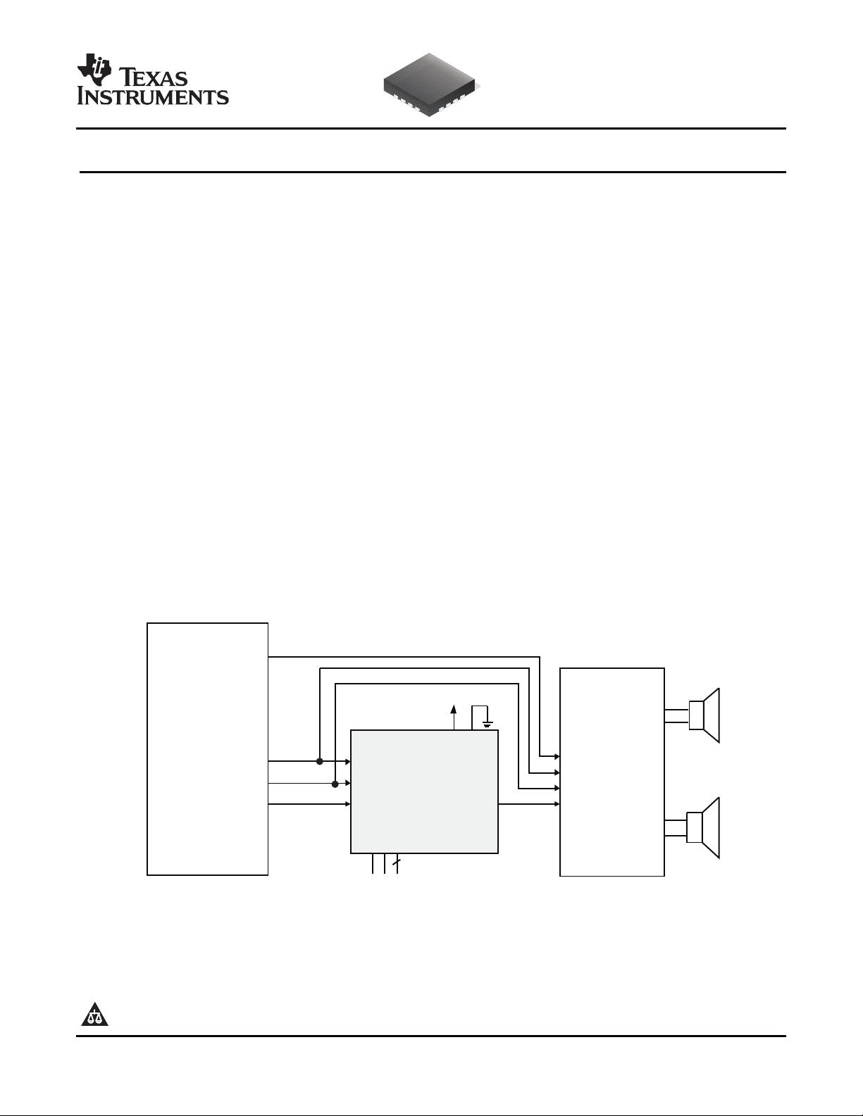
DESCRIPTION
The TPA5050 accepts a single serial audio input,
buffers the data for a selectable period of time, and
outputs the delayed audio data on a single serial
output. One device allows delay of up to 170 ms/ch
(fs = 48 kHz) to synchronize the audio stream to the
video stream in systems with complex video
processing algorithms. If more delay is needed, the
devices can be connected in series.
SIMPLIFIED APPLICATION DIAGRAM
Please be aware that an important notice concerning availability, standard warranty, and use in critical applications of Texas Instruments semiconductor products and disclaimers thereto appears at the end of this data sheet.
PRODUCTION DATA information is current as of publication date.
Products conform to specifications per the terms of the Texas
Instruments standard warranty. Production processing does not
necessarily include testing of all parameters.
Copyright © 2006–2007, Texas Instruments Incorporated
Page 2
www.ti.com
BCLK
DATA_OUT
GND
VDD
ADD1
LRCLK
SCL
GND
ADD0
ADD2
GND
DATA
7
5
6
11
9
10
12
16
15
14
13
3
1
2
4
SDA
8
GND
GND
GND
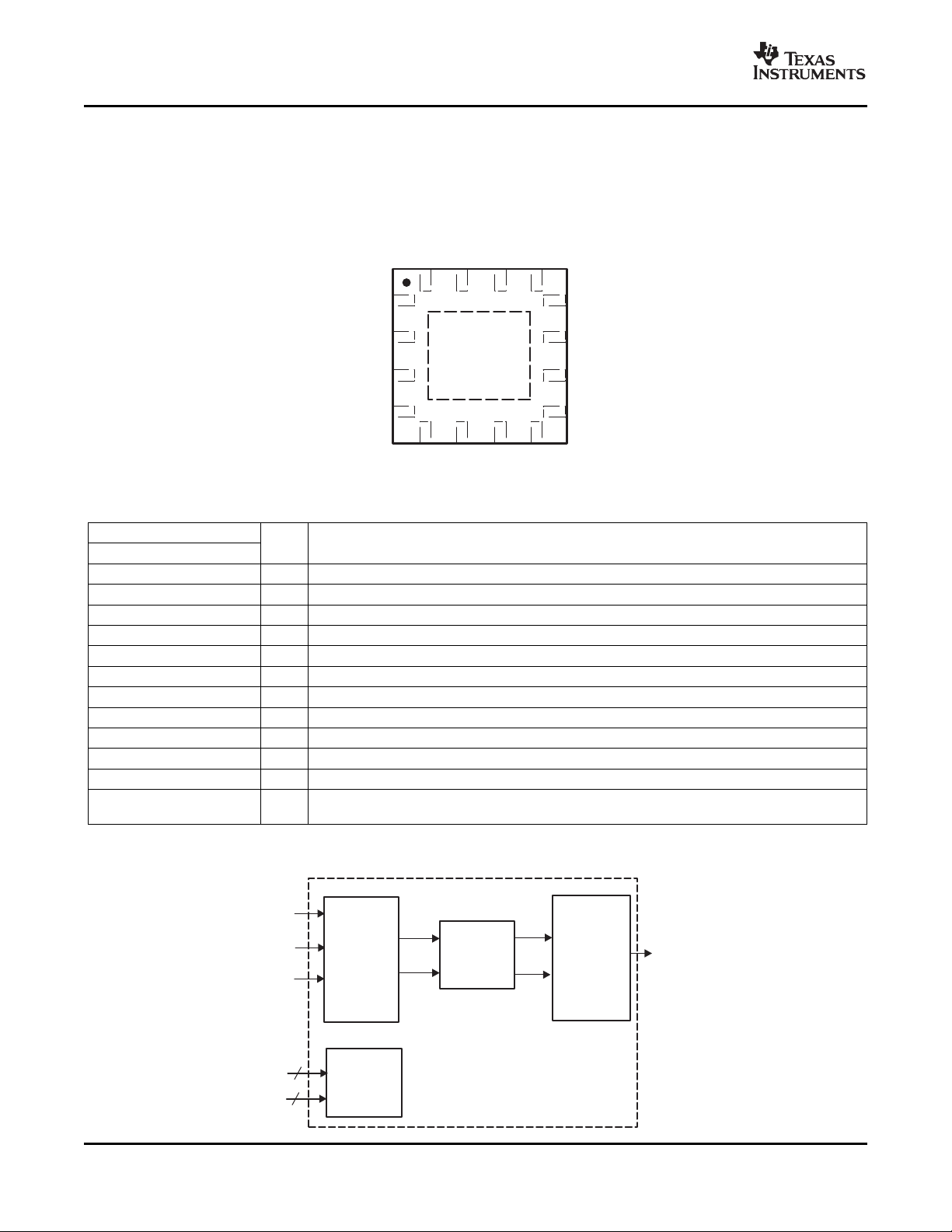
RSA (QFN)PACKAGE
(TOP VIEW)
DATA
BCLK
LRCLK
INPUT
BUFFER
OUTPUT
BUFFER
DATA_OUT
CONTROL
2
3
I C
2
ADDx(2:0)
DELAY
MEMORY
TPA5050
SLOS492B – MAY 2006 – REVISED MAY 2007
PIN DESCRIPTIONS
TERMINAL FUNCTIONS
TERMINAL
NAME NO.
ADD0 10 I I2C address select pin – LSB
ADD1 11 I I2C address select pin
ADD2 12 I I2C address select pin – MSB
BCLK 16 I Audio data bit clock input for serial input. 5V tolerant input.
DATA 2 I Audio serial data input for serial input. 5V tolerant input.
DATA_OUT 15 O Delayed audio serial data output.
GND 5–9, 14 P Ground – All ground terminals must be tied to GND for proper operation
LRCLK 1 I Left and Right serial audio sampling rate clock (fs). 5V tolerant input.
SCL 3 I I2C communication bus clock input. 5V tolerant input.
SDA 4 I/O I2C communication bus data input. 5V tolerant input.
VDD 13 P Power supply interface.
Thermal Pad -
I/O DESCRIPTION
Connect to ground. Must be soldered down in all applications to properly secure device on the
PCB.
FUNCTIONAL BLOCK DIAGRAM
2
Submit Documentation Feedback
Page 3
www.ti.com
SLOS492B – MAY 2006 – REVISED MAY 2007
ABSOLUTE MAXIMUM RATINGS
over operating free-air temperature (unless otherwise noted)
V
Supply voltage –0.3 to 3.6 V
DD
V
Input voltage
I
Continuous total power dissipation See Dissipation Rating Table
T
Operating free-air temperature range –40 to 85 ° C
A
T
Operating junction temperature range –40 to 125 ° C
J
T
Storage temperature range –65 to 125 ° C
stg
Lead temperature 1,6 mm (1/16 inch) from case for 10 seconds 260 ° C
(1) Stresses beyond those listed under absolute maximum ratings may cause permanent damage to the device. These are stress ratings
only, and functional operations of the device at these or any other conditions beyond those indicated under recommended operating
conditions is not implied. Exposure to absolute-maximum-rated conditions for extended periods may affect device reliability.
DATA, LRCLK, BCLK, SCL, SDA –0.3 to 5.5 V
ADD[2:0] –0.3 to VDD+0.3
(1)
VALUE UNIT
TPA5050
DISSIPATION RATINGS
(1)
PACKAGE TA≤ 25 ° C DERATING TA= 70 ° C TA= 85 ° C
POWER RATING FACTOR POWER RATING POWER RATING
RSA 2.5 W 25mW/ ° C 1.375 W 1.0 W
(1) This data was taken using 1 oz trace and copper pad that is soldered directly to a JEDEC standard high-k PCB. The thermal pad must
be soldered to a thermal land on the printed-circuit board. See TI Technical Briefs SCBA017 D and SLUA271 for more information about
using the QFN thermal pad.
RECOMMENDED OPERATING CONDITIONS
MIN MAX UNIT
V
V
V
T
Supply voltage VDD 3 3.6 V
DD
High-level input voltage DATA, LRCLK, BCLK, SCL, SDA, ADD[2:0] 2 V
IH
Low-level input voltage DATA, LRCLK, BCLK, SCL, SDA, ADD[2:0] 0.8 V
IL
Operating free-air temperature –40 85 ° C
A
Submit Documentation Feedback
3
Page 4
www.ti.com
SCL
SDA
t
w(H)
t
w(L)
t
su1
t
h1
SCL
SDA
th2 t(buf)
tsu2 tsu3
StartCondition
StopCondition
TPA5050
SLOS492B – MAY 2006 – REVISED MAY 2007
DC CHARACTERISTICS
TA= 25 ° C, V
I
DD
I
OH
I
OL
I
IH
I
IL
= 3 V (unless otherwise noted)
DD
PARAMETER TEST CONDITIONS MIN TYP MAX UNIT
Supply current V
High-level output current DATA_OUT = 2.6 V 7 13 mA
Low-level output current DATA_OUT = 0.4 V 7 13 mA
High-level input current µ A
Low-level input current 1 µ A
= 3.3 V, fs = 48 kHz, BCLK = 32 fs 1.5 3 mA
DD
DATA, LRCLK, BCLK, SCL, SDA, Vi = 5.5V, VDD = 3V 20
ADD[2:0], Vi = 3.6V, VDD = 3.6V 5
DATA, LRCLK, BCLK, SCL, SDA, ADD[2:0], Vi = 0V,
VDD = 3.6V
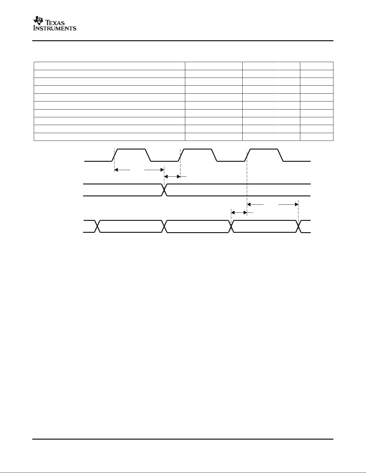
TIMING CHARACTERISTICS
(1) (2)
For I2C Interface Signals Over Recommended Operating Conditions (unless otherwise noted)
PARAMETER TEST CONDITIONS MIN TYP MAX UNIT
f
Frequency, SCL No wait states 400 kHz
SCL
t
Pulse duration, SCL high 0.6 µ s
w(H)
t
Pulse duration, SCL low 1.3 µ s
w(L)
t
Setup time, SDA to SCL 100 ns
su1
t
Hold time, SCL to SDA 10 ns
h1
t
Bus free time between stop and start condition 1.3 µ s
(buf)
t
Setup time, SCL to start condition 0.6 µ s
su2
t
Hold time, start condition to SCL 0.6 µ s
h2
t
Setup time, SCL to stop condition 0.6 µ s
su3
(1) V
(2) A pull-up resistor ≤ 2 k Ω is required for a 5 V I2C bus voltage.
= V
Pull-up
DD
4
Figure 1. SCL and SDA Timing
Figure 2. Start and Stop Conditions Timing
Submit Documentation Feedback
Page 5
www.ti.com
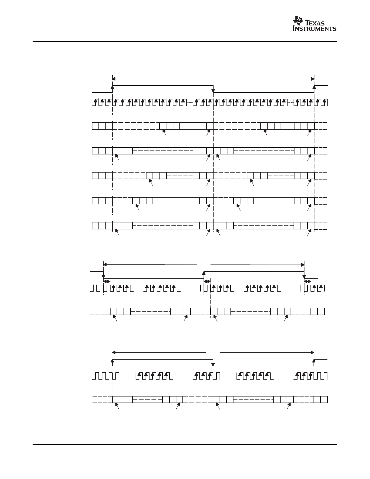
Serial Audio Input Ports
t
h1
t
su1
t
su2
t
h2
DATA
BCLK
(Input)
LRCLK
(Input)
over recommended operating conditions (unless otherwise noted)
PARAMETER TEST CONDITIONS MIN TYP MAX UNIT
f
Frequency, BCLK 32 × fs, 48 × fs, 64 × fs 1.024 12.288 MHz
SCLKIN
t
Setup time, LRCLK to BCLK rising edge 10 ns
su1
t
Hold time, LRCLK from BCLK rising edge 10 ns
h1
t
Setup time, DATA to BCLK rising edge 10 ns
su2
t
Hold time, DATA from BCLK rising edge 10 ns
h2
LRCLK frequency 32 48 192 kHz
BCLK duty cycle 50%
LRCLK duty cycle 50%
BCLK rising edges between LRCLK rising edges LRCLK duty cycle = 50% 32 64 BCLK edges
TPA5050
SLOS492B – MAY 2006 – REVISED MAY 2007
Figure 3. Serial Data Interface Timing
APPLICATION INFORMATION
AUDIO SERIAL INTERFACE
The audio serial interface for the TPA5050 consists of a 3-wire synchronous serial port. It includes LRCLK,
BCLK, and DATA. BCLK is the serial audio bit clock, and it is used to clock the serial data present on DATA into
the serial shift register of the audio interface. Serial data is clocked into the TPA5050 on the rising edge of
BCLK. LRCLK is the serial audio left/right word clock. It is used to latch serial data into the internal registers of
the serial audio interface. LRCLK is operated at the sampling frequency, fs. BCLK can be operated at 32 to 64
times the sampling frequency for right-justified, left-justified, and I2S formats. A system clock is not necessary for
the operation of the TPA5050.
AUDIO DATA FORMATS AND TIMING
The TPA5050 supports industry-standard audio data formats, including right-justified, I2S, and left-justified. The
data formats are shown in Figure 4 . Data formats are selected using the I2C interface and register map (see
Table 1 ).
Submit Documentation Feedback
5
Page 6
www.ti.com
LRCK
(2)I2SDataFormat;L-Channel=LOW,R-Channel=HIGH
MSB LSB
1/f
S
(= 32fS,48fS,or64fS)
18-BitRight-Justified,BCK=48fSor64f
S
1/f
S
(1) Right-JustifiedDataFormat;L-Channel=HIGH,R-Channel=LOW
(3)Left-JustifiedDataFormat;L-Channel=HIGH,R-Channel=LOW
MSB LSB
20-Bit Right-Justified,BCK=48fSor64f
S
MSB LSB
24-BitRight-Justified,BCK=48fSor64f
S
1/f
S
(=32fS,48fS,or64fS)
(=32fS,48fS,or64fS)
MSB LSB
16-BitRight-Justified,BCK=32f
S
16-BitRight-Justified,BCK=48fSor64f
S
MSB LSB
L-Channel R-Channel
BCK
DATA 14 15 16
1 2 3 14 15 16
14 15 16 1 2 3 14 15 16
16 17 18
DATA
DATA
DATA
DATA
1 2 3 16 17 18
18 19 20 1 2 3 18 19 20
22 23 24 1 2 3
MSB LSB
MSB LSB
MSB LSB
MSB LSB
1 2 3 14 15 16
1 2 3 14 15 16
1 2 3 16 17 18
1 2 3 18 19 20
22 23 24
MSB LSB
1 2 3 22 23 24
L-Channel R-ChannelLRCK
BCK
DATA
1 2 3 1 2
MSB
N–2NN–1
LSB
1 2 3
MSB
N–2NN–1
LSB
L-Channel R-Channel
LRCK
BCK
DATA 1 2 3
N–2NN–1
1 2 3
N–2NN–1
1 2
MSB LSB LSBMSB
TPA5050
SLOS492B – MAY 2006 – REVISED MAY 2007
APPLICATION INFORMATION (continued)
6
Figure 4. Audio Data Formats
Submit Documentation Feedback
Page 7
www.ti.com
Register(N)
8-BitDatafor 8-BitDatafor
Register(N+1)
TPA5050
SLOS492B – MAY 2006 – REVISED MAY 2007
APPLICATION INFORMATION (continued)
GENERAL I2C OPERATION
The I2C bus employs two signals; SDA (data) and SCL (clock), to communicate between integrated circuits in a
system. Data is transferred on the bus serially, one bit at a time. The address and data are transferred in byte
(8-bit) format with the most-significant bit (MSB) transferred first. In addition, each byte transferred on the bus is
acknowledged by the receiving device with an acknowledge bit. Each transfer operation begins with the master
device driving a start condition on the bus and ends with the master device driving a stop condition on the bus.
The bus uses transitions on the data terminal (SDA) while the clock is high to indicate start and stop conditions.
A high-to-low transition on SDA indicates a start and a low-to-high transition indicates a stop. Normal data-bit
transitions must occur within the low time of the clock period. These conditions are shown in Figure 5 . The
master generates the 7-bit slave address and the read/write (R/W) bit to open communication with another
device and then wait for an acknowledge condition. The TPA5050 holds SDA low during acknowledge clock
period to indicate an acknowledgement. When this occurs, the master transmits the next byte of the sequence.
Each device is addressed by a unique 7-bit slave address plus R/W bit (1 byte). All compatible devices share
the same signals via a bidirectional bus using a wired-AND connection.
An external pull-up resistor must be used for the SDA and SCL signals to set the HIGH level for the bus. When
the bus level is 5 V, pull-up resistors between 1 k Ω and 2 k Ω in value must be used.
Figure 5. Typical I2C Sequence
There is no limit on the number of bytes that can be transmitted between start and stop conditions. When the
last word transfers, the master generates a stop condition to release the bus. A generic data transfer sequence
is shown in Figure 5 .
The 7-bit address for the TPA5050 is selectable using the 3 address pins (ADD2, ADD1, ADD0). Table 1 lists
the 8 possible slave addresses.
Table 1. I2C Slave Address
FIXED ADDRESS
(4 MSB bits)
1101 0 0 0
1101 0 0 1
1101 0 1 0
1101 0 1 1
1101 1 0 0
1101 1 0 1
1101 1 1 0
1101 1 1 1
ADD2 ADD1 ADD0
SELECTABLE ADDRESS BITS
SINGLE-AND MULTIPLE-BYTE TRANSFERS
The serial control interface supports both single-byte and multi-byte read/write operations for all registers.
During multiple-byte read operations, the TPA5050 responds with data, a byte at a time, starting at the register
assigned, as long as the master device continues to respond with acknowledges.
Submit Documentation Feedback
7
Page 8

www.ti.com
A6 A5 A4 A3 A2 A1 A0
R/W
ACK A7 A6 A5 A4 A3 A2 A1 A0 ACK D7 D6 D5 D4 D3 D2 D1 D0 ACK
Start
Condition
Stop
Condition
Acknowledge Acknowledge Acknowledge
I
2
CDeviceAddressand
Read/WriteBit
Register DataByte
Register
TPA5050
SLOS492B – MAY 2006 – REVISED MAY 2007
The TPA5050 supports sequential I2C addressing. For write transactions, if a register is issued followed by data
for that register and all the remaining registers that follow, a sequential I2C write transaction has taken place. For
I2C sequential write transactions, the register issued then serves as the starting point, and the amount of data
subsequently transmitted, before a stop or start is transmitted, determines to how many registers are written.
SINGLE-BYTE WRITE
As shown is Figure 6 , a single-byte data write transfer begins with the master device transmitting a start
condition followed by the I2C device address and the read/write bit. The read/write bit determines the direction of
the data transfer. For a write data transfer, the read/write bit must be set to 0. After receiving the correct I2C
device address and the read/write bit, the TPA5050 responds with an acknowledge bit. Next, the master
transmits the register byte corresponding to the TPA5050 internal memory address being accessed. After
receiving the register byte, the TPA5050 again responds with an acknowledge bit. Next, the master device
transmits the data byte to be written to the memory address being accessed. After receiving the data byte, the
TPA5050 again responds with an acknowledge bit. Finally, the master device transmits a stop condition to
complete the single-byte data write transfer.
Figure 6. Single-Byte Write Transfer
MULTIPLE-BYTE WRITE AND INCREMENTAL MULTIPLE-BYTE WRITE
A multiple-byte data write transfer is identical to a single-byte data write transfer except that multiple data bytes
are transmitted by the master device to the TPA5050 as shown in Figure 7 . After receiving each data byte, the
TPA5050 responds with an acknowledge bit.
Figure 7. Multiple-Byte Write Transfer
SINGLE-BYTE READ
As shown in Figure 8 , a single-byte data read transfer begins with the master device transmitting a start
condition followed by the I2C device address and the read/write bit. For the data read transfer, both a write
followed by a read are actually done. Initially, a write is done to transfer the address byte of the internal memory
address to be read. As a result, the read/write bit is set to a 0.
After receiving the TPA5050 address and the read/write bit, the TPA5050 responds with an acknowledge bit.
The master then sends the internal memory address byte, after which the TPA5050 issues an acknowledge bit.
The master device transmits another start condition followed by the TPA5050 address and the read/write bit
again. This time the read/write bit is set to 1, indicating a read transfer. Next, the TPA5050 transmits the data
byte from the memory address being read. After receiving the data byte, the master device transmits a
not-acknowledge followed by a stop condition to complete the single-byte data read transfer.
8
Submit Documentation Feedback
Page 9

www.ti.com
A6 A5 A0 R/W ACK A7 A6 A5 A4 A0 ACK A6 A5 A0 ACK
Start
Condition
Stop
Condition
Acknowledge Acknowledge Acknowledge
I
2
CDeviceAddressand
Read/WriteBit
Register DataByte
D7 D6 D1 D0 ACK
I2CDeviceAddressand
Read/WriteBit
Not
Acknowledge
R/WA1 A1
RepeatStart
Condition
A6 A0 ACK
Acknowledge
I2CDeviceAddressand
Read/WriteBit
R/WA6 A0 R/W ACK A0 ACK D7 D0 ACK
Start
Condition
Stop
Condition
Acknowledge Acknowledge Acknowledge
LastDataByte
ACK
FirstDataByte
RepeatStart
Condition
Not
Acknowledge
I
2
CDeviceAddressand
Read/WriteBit
Register
OtherDataBytes
A7 A6 A5 D7 D0 ACK
Acknowledge
D7 D0
VDD
DATA
LRCLK
BCLK
GND
DATA_OUT
SDA
SCL
ADD0
ADD1
ADD2
GND
3.3V
0.1 Fm
Digital Audio
WordClock
BitClock
Delayed Audio
I CClock
2
I CData
2
I C Address
Select
2
TPA5050
SLOS492B – MAY 2006 – REVISED MAY 2007
Figure 8. Single-Byte Read Transfer
MULTIPLE-BYTE READ
A multiple-byte data read transfer is identical to a single-byte data read transfer except that multiple data bytes
are transmitted by the TPA5050 to the master device as shown in Figure 9 . With the exception of the last data
byte, the master device responds with an acknowledge bit after receiving each data byte.
Figure 9. Multiple-Byte Read Transfer
TPA5050 Operation
The following sections describe the registers configurable via I2C commands for the TPA5050.
Only a single decoupling capacitor (0.1 µ F–1 µ F) is required across VDD and GND. The ADDx terminals can be
directly connected to VDD or GND. Table 1 describes the I2C addresses selectable via the ADDx terminals. A
schematic implementation of the TPA5050 is shown in Figure 10 .
Figure 10. TPA5050 Schematic
Submit Documentation Feedback
9
Page 10

www.ti.com
TPA5050
SLOS492B – MAY 2006 – REVISED MAY 2007
SERIAL CONTROL INTERFACE REGISTER SUMMARY
Table 2. Serial Control Register Summary
REGISTER REGISTER NAME NO. OF CONTENTS INITIALIZATION
0x01 Control Register 1 Description shown in subsequent section 00
0x02 Right Delay Upper (5 bits) 1 Description shown in subsequent section 00
0x03 Right Delay Lower (8 bits) 1 Description shown in subsequent section 00
0x04 Left Delay Upper (5 bits) 1 Description shown in subsequent section 00
0x05 Left Delay Lower (8 bits) 1 Description shown in subsequent section 00
0x06 Frame Delay 1 Description shown in subsequent section 00
0x07 RJ Packet Length 1 Description shown in subsequent section 00
0x08 Complete Update 1 Description shown in subsequent section 00
CONTROL REGISTER (0x01)
The control register allows the user to mute a specific audio channel. It is also used to specify the data type (I2S,
Right-Justified, or Left-Justified.
BYTES VALUE
Table 3. Control Registers (0x01)
D7 D6 D5 D4 D3 D2 D1 D0 FUNCTION
0 0 X X X X – – Left and Right channel are active.
0 1 X X X X – – Left channel is MUTED.
1 0 X X X X – – Right channel is MUTED.
1 1 X X X X – – Left and Right channel are MUTED.
– – X X X X 0 0 I2S data format
– – X X X X 0 1 Right-justified data format (see PACKET LENGTH register 0x07)
– – X X X X 1 0 Left-justified data format
– – X X X X 1 1 Bypass mode – data is passed straight through without delay.
(1) Default values are in bold.
(1)
AUDIO DELAY REGISTERS (0x02–0x05)
The audio delay for the left and right channels is fixed by writing a total of 13 bits (2 byte transfer) to upper and
lower registers as specified in Table 1 . A multiple byte transfer should be performed starting with the control
register and following with 4 bytes to fill the upper and lower registers associated with right/left channel delay.
The decimal value of D0–D12 equals the number of samples to delay. The maximum number of delayed
samples is 8191 for the TPA5050. This equates to 170.65 ms [8191 × (1/fs)] at 48 kHz.
Table 4. Audio Delay Registers (0x02–0x05)
D12 D11 D10–D2 D1 D0 FUNCTION
0 0 0 0 0 Left and Right audio is passed to output with no delay.
0 0 0 0 1 Left and Right audio is delayed by 1 sample (1/fs = delay time)
1 1 1 1 1 Left and Right audio is delayed by 8191 samples (8191/fs = delay time)
(1) Default values are in bold.
(1)
FRAME DELAY REGISTERS (0x06)
This register can be used to specify delay in video frames instead of audio samples. When the MSB is set to 1,
the audio delay registers (0x01–0x04) are bypassed and the Frame Delay Register is used to set the delay
based on the frame rate (D6), audio sample rate (D5–D3), and number of frames to delay (D2–D0).
The total audio delay time is calculated by the following formula:
Audio Delay (in samples) = int [# Delay Frames × (1/Frame Rate) × Audio Sample Rate]
10
Submit Documentation Feedback
Page 11

www.ti.com
SLOS492B – MAY 2006 – REVISED MAY 2007
If the result of the formula above is greater than the maximum number of delay samples (8191 for TPA5050),
then the value is limited to this maximum before passing to the delay block.
TPA5050
Table 5. Frame Delay Registers (0x06)
D7 D6 D5 D4 D3 D2 D1 D0 FUNCTION
0 Settings in this register are masked and audio delay is determined by
settings in the right/left audio delay registers.
1 Right/left audio delay registers are masked and delay is determined by settings in
this register.
0 Frame rate = 50 Hz
1 Frame rate = 59.94 Hz
0 0 0 Audio sample rate = 32 kHz
0 0 1 Audio sample rate = 44.1 kHz
0 1 0 Audio sample rate = 48 kHz
0 1 1 Audio sample rate = 88.2 kHz
1 0 0 Audio sample rate = 96 kHz
1 0 1 Audio sample rate = 176.4 kHz
1 1 0 Audio sample rate = 192 kHz
1 1 1 Audio sample rate = 192 kHz
0 0 0 Delay frames = 1
0 0 1 Delay frames = 2
1 1 1 Delay frames = 8
(1) Default values are in bold.
(1)
RJ PACKET LENGTH REGISTERS (0x07)
This register is only used in right justified mode. The decimal value of bits [5:0] represents the width of the
useable data in a right justified audio stream. The number of BCLK transitions between LRCLK transitions must
be greater than or equal to the packet length selected in this register. The maximum packet length value is 24
bits. Any setting greater whose numerical value is greater than 24 bits is limited to the maximum 24 bits.
Table 6. RJ Package Length (0x07)
D5 D4 D3 D2 D1 D0 FUNCTION
0 0 0 0 0 0 Packet length = 0 bits
0 0 0 0 0 1 Packet length = 1 bits
0 1 1 X X X Packet length = 24 bits
(1) Default values are in bold.
(1)
COMPLETE UPDATE REGISTER (0x08)
Since the audio delay values are divided among several registers, it is likely that multiple writes would be
necessary to configure the device. This may cause interruptions in the audio stream and unwanted pops and
clicks might occur as register data is passed to delay functional block.
To avoid this from happening, the Complete Update register is used to transfer the user settings from the
register file to the delay functional block when a 1 is written to the LSB. For example, if the right delay is set to
35 samples, and the left delay is set to 300 samples, the device holds the right channel in MUTE until 35
samples of audio data have passed, and holds the left channel in MUTE until 300 samples of audio data have
passed.
Note that the individual channels can be muted using the upper bits of the Control Registers without writing to
the Complete Update registers.
Submit Documentation Feedback
11
Page 12

www.ti.com
D2Start ACK 01 ACK C0 ACK Stop
TPA5050 Addressand
Write
Register Address Data
D2Start
ACK
01
00
0F
ACK
Stop
TPA5050 Addressand
Write
Register Address
(ControlRegister)
Data
(RightDelayUpperBits)
ACK
ACK
FF
ACK
Data
(ControlRegister)
Data
(RightDelayLowerBits)
10
ACK
00
00
00
ACK
Data
(LeftDelayUpperBits)
Data
(RJPacket=0Bits)
ACK
ACK
01
ACK
Data
(FrameDelay)
Data
(CompleteUpdate)
Data
(LeftDelayLowerBits)
D2
Start ACK 01 ACK 01 ACK Stop
TPA5050 Addressand
Write
Register Address
(ControlRegister)
Data
(ControlRegister)
D2Start ACK 06 ACK 91 ACK 10
TPA5050 Addressand
Write
Register Address
(FrameDelay)
Data
(FrameDelay)
01
ACK
Data
(RJPacket=16Bits)
Stop
Data
(CompleteUpdate)
ACK
TPA5050
SLOS492B – MAY 2006 – REVISED MAY 2007
Table 7. Complete Update Registers (0x08)
D7–D1 D0 FUNCTION
X 0 No data from the register settings is passed to the delay block.
X 1 Stream type, right/left delay or frame delay, and packet length is passed to the delay functional block.
(1) Default values are in bold.
APPLICATION EXAMPLES
The following are some examples of I2C commands used to read or write to the TPA5050. For all conditions,
assume the address of the TPA5050 is set to 001.
Single Byte Write
In this example, the TPA5050 is set to mute both left and right channels, and to operate in I2S mode.
Multiple Byte Write
In this example, the TPA5050 is set to make both the left and right channels active, operate in I2S mode, delay
the right channel by 4095 samples, and delay the left channel by 4096 samples. This is a sequential write, so all
registers must have data written to them.
(1)
Combination Single Byte Write and Sequential Write
In this example, the TPA5050 is set to operate in the Right Justified mode, with a packet length of 16 bits. The
device is to delay the audio signal by 40 ms using the Frame Delay function. Assume the audio sample rate (fs)
= 48 kHz, and the Frame rate = 50 Hz. This is a combination of single writes and a sequential write. Since the
Right Justified mode is set in the Control Register, and the Frame Delay is set in register 0x06, the data in
registers 0x02–0x05 can be ignored.
Note that in every circumstance where a delay was written into the memory of the TPA5050, a 1 must be written
to the Complete Data register for the change to take effect. This does not apply to muting, which occurs in the
Control register.
12
Submit Documentation Feedback
Page 13

www.ti.com
D2
Start
ACK
01
ACK Start
D3
XX
TPA5050 Addressand
Write
Register Address
(ControlRegister)
Stop
ACK
DataRead
(ControlRegister)
No
ACK
TPA5050 Addressand
Read
XX
ACK
XX
XX
XX
DataRead
(FrameDelay)
DataRead
(LeftDelayUpper)
ACK
ACK
XX
ACK
DataRead
(RightDelayLower)
D2
Start
ACK
01
Start
ACK
D3
TPA5050 Addressand
Read
Register Address
(ControlRegister)
ACK
XX
ACK
XX
DataRead
(ControlRegister)
TPA5050 Addressand
Write
ACK
XX
Stop
No
ACK
DataRead
(CompleteUpdate)
DataRead
(LeftDelayLower)
DataRead
(RJPacketLength)
ACK
DataRead
(RightDelayUpper)
TPA5050
SLOS492B – MAY 2006 – REVISED MAY 2007
Single Byte Read
In this example, one byte of data is read from the Control Register (0x01). After the data (represented xx) by is
read by the master device, the master device issues a Not Acknowledge, before stopping the communication.
Multiple Byte Read
Often, when it is necessary to read what is contained in one register, it is necessary to determine what
information is contained in all registers. In such a case, a sequential read should be used. In situations where
data must be read from a register at the beginning (0x01), and a register towards the end (0x07), a sequential
read is likely to be faster to implement than multiple single byte reads.
In this example, a sequential read is initiated with the Control Register (0x01), and ends with the Complete
Update Register (0x08).
Submit Documentation Feedback
13
Page 14

www.ti.com
0
0.5
1
1.5
2
2.5
3
3.5
4
4.5
5
32 52 72 92 112 132 152 172 192
fs-SamplingFrequency-kHz
I
-SupplyCurrent-mA
DD
V =3.6V
DD
V =3.3V
DD
V =3V
DD
BCLK=64fs
Data=24bit
SUPPLY CURRENT
vs
SAMPLINGFREQUENCY
TPA5050
SLOS492B – MAY 2006 – REVISED MAY 2007
DEVICE CURRENT CONSUMPTION
The TPA5050 draws different amounts of supply current depending upon the conditions under which it is
operated. As V
the sampling frequency, fs. An increase in fs causes an increase in IDD. Figure 11 illustrates the relationship
between operating condition and typical supply current.
increases, so too does IDD. Likewise, as V
DD
decreases, IDDdecreases. The same is true of
DD
Figure 11. Typical Supply Current
14
Submit Documentation Feedback
Page 15

PACKAGE OPTION ADDENDUM
www.ti.com
21-May-2007
PACKAGING INFORMATION
Orderable Device Status
(1)
Package
Type
Package
Drawing
Pins Package
Qty
Eco Plan
TPA5050RSAR ACTIVE QFN RSA 16 3000 Green (RoHS &
no Sb/Br)
TPA5050RSARG4 ACTIVE QFN RSA 16 3000 Green (RoHS &
no Sb/Br)
TPA5050RSAT ACTIVE QFN RSA 16 250 Green (RoHS &
no Sb/Br)
TPA5050RSATG4 ACTIVE QFN RSA 16 250 Green (RoHS &
no Sb/Br)
(1)
The marketing status values are defined as follows:
ACTIVE: Product device recommended for new designs.
LIFEBUY: TI has announced that the device will be discontinued, and a lifetime-buy period is in effect.
NRND: Not recommended for new designs. Device is in production to support existing customers, but TI does not recommend using this part in
a new design.
PREVIEW: Device has been announced but is not in production. Samples may or may not be available.
OBSOLETE: TI has discontinued the production of the device.
(2)
Eco Plan - The planned eco-friendly classification: Pb-Free (RoHS), Pb-Free (RoHS Exempt), or Green (RoHS & no Sb/Br) - please check
http://www.ti.com/productcontent for the latest availability information and additional product content details.
TBD: The Pb-Free/Green conversion plan has not been defined.
Pb-Free (RoHS): TI's terms "Lead-Free" or "Pb-Free" mean semiconductor products that are compatible with the current RoHS requirements
for all 6 substances, including the requirement that lead not exceed 0.1% by weight in homogeneous materials. Where designed to be soldered
at high temperatures, TI Pb-Free products are suitable for use in specified lead-free processes.
Pb-Free (RoHS Exempt): This component has a RoHS exemption for either 1) lead-based flip-chip solder bumps used between the die and
package, or 2) lead-based die adhesive used between the die and leadframe. The component is otherwise considered Pb-Free (RoHS
compatible) as defined above.
Green (RoHS & no Sb/Br): TI defines "Green" to mean Pb-Free (RoHS compatible), and free of Bromine (Br) and Antimony (Sb) based flame
retardants (Br or Sb do not exceed 0.1% by weight in homogeneous material)
(2)
Lead/Ball Finish MSL PeakTemp
CU NIPDAU Level-2-260C-1 YEAR
CU NIPDAU Level-2-260C-1 YEAR
CU NIPDAU Level-2-260C-1 YEAR
CU NIPDAU Level-2-260C-1 YEAR
(3)
(3)
MSL, Peak Temp. -- The Moisture Sensitivity Level rating according to the JEDEC industry standard classifications, and peak solder
temperature.
Important Information and Disclaimer:The information provided on this page represents TI's knowledge and belief as of the date that it is
provided. TI bases its knowledge and belief on information provided by third parties, and makes no representation or warranty as to the
accuracy of such information. Efforts are underway to better integrate information from third parties. TI has taken and continues to take
reasonable steps to provide representative and accurate information but may not have conducted destructive testing or chemical analysis on
incoming materials and chemicals. TI and TI suppliers consider certain information to be proprietary, and thus CAS numbers and other limited
information may not be available for release.
In no event shall TI's liability arising out of such information exceed the total purchase price of the TI part(s) at issue in this document sold by TI
to Customer on an annual basis.
Addendum-Page 1
Page 16

PACKAGE MATERIALS INFORMATION
www.ti.com
TAPE AND REEL INFORMATION
11-Mar-2008
*All dimensions are nominal
Device Package
TPA5050RSAR QFN RSA 16 3000 330.0 12.4 4.3 4.3 1.5 8.0 12.0 Q2
TPA5050RSAT QFN RSA 16 250 180.0 12.4 4.3 4.3 1.5 8.0 12.0 Q2
Type
Package
Drawing
Pins SPQ Reel
Diameter
(mm)
Reel
Width
W1 (mm)
A0 (mm) B0 (mm) K0 (mm) P1
(mm)W(mm)
Pin1
Quadrant
Pack Materials-Page 1
Page 17

PACKAGE MATERIALS INFORMATION
www.ti.com
11-Mar-2008
*All dimensions are nominal
Device Package Type Package Drawing Pins SPQ Length (mm) Width (mm) Height (mm)
TPA5050RSAR QFN RSA 16 3000 346.0 346.0 29.0
TPA5050RSAT QFN RSA 16 250 190.5 212.7 31.8
Pack Materials-Page 2
Page 18

Page 19

Page 20

Page 21

IMPORTANT NOTICE
Texas Instruments Incorporated and its subsidiaries (TI) reserve the right to make corrections, modifications, enhancements, improvements,
and other changes to its products and services at any time and to discontinue any product or service without notice. Customers should
obtain the latest relevant information before placing orders and should verify that such information is current and complete. All products are
sold subject to TI’s terms and conditions of sale supplied at the time of order acknowledgment.
TI warrants performance of its hardware products to the specifications applicable at the time of sale in accordance with TI’s standard
warranty. Testing and other quality control techniques are used to the extent TI deems necessary to support this warranty. Except where
mandated by government requirements, testing of all parameters of each product is not necessarily performed.
TI assumes no liability for applications assistance or customer product design. Customers are responsible for their products and
applications using TI components. To minimize the risks associated with customer products and applications, customers should provide
adequate design and operating safeguards.
TI does not warrant or represent that any license, either express or implied, is granted under any TI patent right, copyright, mask work right,
or other TI intellectual property right relating to any combination, machine, or process in which TI products or services are used. Information
published by TI regarding third-party products or services does not constitute a license from TI to use such products or services or a
warranty or endorsement thereof. Use of such information may require a license from a third party under the patents or other intellectual
property of the third party, or a license from TI under the patents or other intellectual property of TI.
Reproduction of TI information in TI data books or data sheets is permissible only if reproduction is without alteration and is accompanied
by all associated warranties, conditions, limitations, and notices. Reproduction of this information with alteration is an unfair and deceptive
business practice. TI is not responsible or liable for such altered documentation. Information of third parties may be subject to additional
restrictions.
Resale of TI products or services with statements different from or beyond the parameters stated by TI for that product or service voids all
express and any implied warranties for the associated TI product or service and is an unfair and deceptive business practice. TI is not
responsible or liable for any such statements.
TI products are not authorized for use in safety-critical applications (such as life support) where a failure of the TI product would reasonably
be expected to cause severe personal injury or death, unless officers of the parties have executed an agreement specifically governing
such use. Buyers represent that they have all necessary expertise in the safety and regulatory ramifications of their applications, and
acknowledge and agree that they are solely responsible for all legal, regulatory and safety-related requirements concerning their products
and any use of TI products in such safety-critical applications, notwithstanding any applications-related information or support that may be
provided by TI. Further, Buyers must fully indemnify TI and its representatives against any damages arising out of the use of TI products in
such safety-critical applications.
TI products are neither designed nor intended for use in military/aerospace applications or environments unless the TI products are
specifically designated by TI as military-grade or "enhanced plastic." Only products designated by TI as military-grade meet military
specifications. Buyers acknowledge and agree that any such use of TI products which TI has not designated as military-grade is solely at
the Buyer's risk, and that they are solely responsible for compliance with all legal and regulatory requirements in connection with such use.
TI products are neither designed nor intended for use in automotive applications or environments unless the specific TI products are
designated by TI as compliant with ISO/TS 16949 requirements. Buyers acknowledge and agree that, if they use any non-designated
products in automotive applications, TI will not be responsible for any failure to meet such requirements.
Following are URLs where you can obtain information on other Texas Instruments products and application solutions:
Products Applications
Amplifiers amplifier.ti.com Audio www.ti.com/audio
Data Converters dataconverter.ti.com Automotive www.ti.com/automotive
DSP dsp.ti.com Broadband www.ti.com/broadband
Clocks and Timers www.ti.com/clocks Digital Control www.ti.com/digitalcontrol
Interface interface.ti.com Medical www.ti.com/medical
Logic logic.ti.com Military www.ti.com/military
Power Mgmt power.ti.com Optical Networking www.ti.com/opticalnetwork
Microcontrollers microcontroller.ti.com Security www.ti.com/security
RFID www.ti-rfid.com Telephony www.ti.com/telephony
RF/IF and ZigBee® Solutions www.ti.com/lprf Video & Imaging www.ti.com/video
Mailing Address: Texas Instruments, Post Office Box 655303, Dallas, Texas 75265
Copyright © 2008, Texas Instruments Incorporated
Wireless www.ti.com/wireless
 Loading...