

TPA4860
1-W MONO AUDIO POWER AMPLIFIER
SLOS164A – SEPTEMBER 1996 – REVISED MARCH 2000
1
POST OFFICE BOX 655303 • DALLAS, TEXAS 75265
D
1-W BTL Output (5 V, 0.2 % THD+N)
D
3.3-V and 5-V Operation
D
No Output Coupling Capacitors Required
D
Shutdown Control (IDD = 0.6 µA)
D
Headphone Interface Logic
D
Uncompensated Gains of 2 to 20 (BTL
Mode)
D
Surface-Mount Packaging
D
Thermal and Short-Circuit Protection
D
High Power Supply Rejection
(56-dB at 1 kHz)
D
LM4860 Drop-In Compatible
description
The TP A4860 is a bridge-tied load (BTL) audio power amplifier capable of delivering 1 W of continuous average
power into an 8-Ω load at 0.4 % THD+N from a 5-V power supply in voiceband frequencies (f < 5 kHz). A BTL
configuration eliminates the need for external coupling capacitors on the output in most applications. Gain is
externally configured by means of two resistors and does not require compensation for settings of 2 to 20.
Features of this amplifier are a shutdown function for power-sensitive applications as well as headphone
interface logic that mutes the output when the speaker drive is not required. Internal thermal and short-circuit
protection increases device reliability . It also includes headphone interface logic circuitry to facilitate headphone
applications. The amplifier is available in a 16-pin SOIC surface-mount package that reduces board space and
facilitates automated assembly.
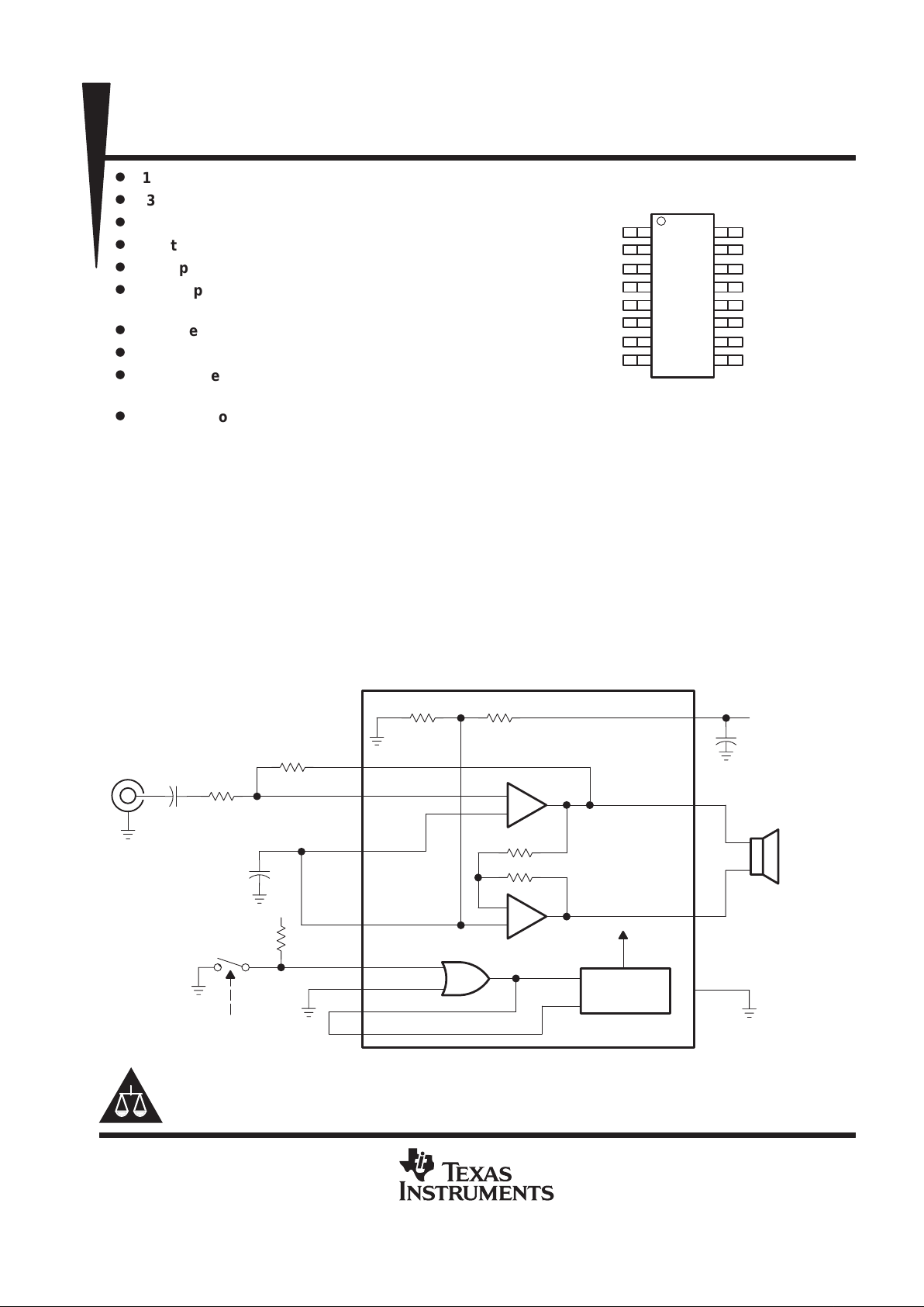
typical application circuit
Audio
Input
Bias
Control
V
DD
1 W
12
10
15
1, 4, 8, 9, 16
VO1
VO2
V
DD
2
3
7
6
5
14
13
11 GAIN
IN+
IN–
BYPASS
HP-IN1
HP-IN2
HP-SENSE
SHUTDOWN
VDD/2
C
I
R
I
R
F
V
DD
R
PU
Headphone
Plug
NC
C
B
C
S
Please be aware that an important notice concerning availability, standard warranty, and use in critical applications of
Texas Instruments semiconductor products and disclaimers thereto appears at the end of this data sheet.
1
2
3
4
5
6
7
8
16
15
14
13
12
11
10
9
GND
SHUTDOWN
HP-SENSE
GND
BYPASS
HP-IN1
HP-IN2
GND
GND
V
O
2
IN+
IN–
V
DD
GAIN
V
O
1
GND
D PACKAGE
(TOP VIEW)
PRODUCTION DATA information is current as of publication date.
Products conform to specifications per the terms of Texas Instruments
standard warranty. Production processing does not necessarily include
testing of all parameters.
Copyright 2000, Texas Instruments Incorporated
TPA4860
1-W MONO AUDIO POWER AMPLIFIER
SLOS164A – SEPTEMBER 1996 – REVISED MARCH 2000
2
POST OFFICE BOX 655303 • DALLAS, TEXAS 75265
AVAILABLE OPTIONS
PACKAGED DEVICE
T
A
SMALL OUTLINE
(D)
–40°C to 85°C TPA4860D
absolute maximum ratings over operating free-air temperature range (unless otherwise noted)
†
Supply voltage, VDD 6 V. . . . . . . . . . . . . . . . . . . . . . . . . . . . . . . . . . . . . . . . . . . . . . . . . . . . . . . . . . . . . . . . . . . . . . . .
Input voltage, VI –0.3 V to VDD +0.3 V. . . . . . . . . . . . . . . . . . . . . . . . . . . . . . . . . . . . . . . . . . . . . . . . . . . . . . . . . . . .
Continuous total power dissipation internally limited (See Dissipation Rating Table). . . . . . . . . . . . . . . . . . . . .
Operating free-air temperature range, TA –40°C to 85°C. . . . . . . . . . . . . . . . . . . . . . . . . . . . . . . . . . . . . . . . . . . .
Storage temperature range, T
stg
–65°C to 150°C. . . . . . . . . . . . . . . . . . . . . . . . . . . . . . . . . . . . . . . . . . . . . . . . . . .
Lead temperature 1,6 mm (1/16 inch) from case for 10 seconds 260°C. . . . . . . . . . . . . . . . . . . . . . . . . . . . . . .
†
Stresses beyond those listed under “absolute maximum ratings” may cause permanent damage to the device. These are stress ratings only, and
functional operation of the device at these or any other conditions beyond those indicated under “recommended operating conditions” is not
implied. Exposure to absolute-maximum-rated conditions for extended periods may affect device reliability.
DISSIPATION RATING TABLE
PACKAGE
TA ≤ 25°C DERATING FACTOR TA = 70°C TA = 85°C
D 1250 mW 10 mW/°C 800 mW 650 mW
recommended operating conditions
MIN MAX UNIT
Supply voltage, V
DD
2.7
5.5
V
p
VDD = 3.3 V
1.25
2.7
V
Common-mode input voltage, V
IC
VDD = 5 V
1.25
4.5
V
Operating free-air temperature, T
A
–40
85
°C
TPA4860
1-W MONO AUDIO POWER AMPLIFIER
SLOS164A – SEPTEMBER 1996 – REVISED MARCH 2000
3
POST OFFICE BOX 655303 • DALLAS, TEXAS 75265
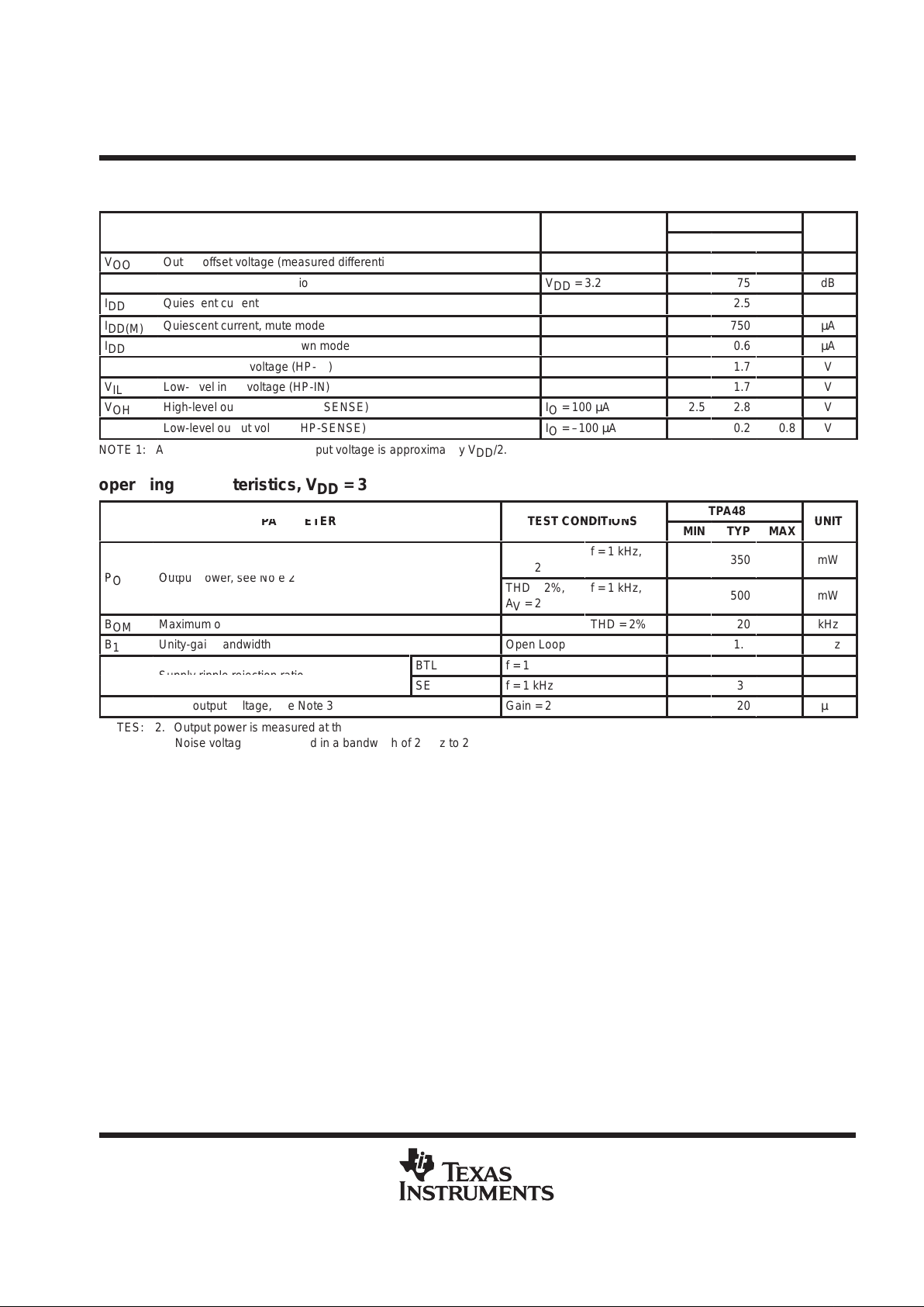
electrical characteristics at specified free-air temperature range, VDD = 3.3 V (unless otherwise
noted)
TPA4860
PARAMETER
TEST CONDITIONS
MIN TYP MAX
UNIT
V
OO
Output offset voltage (measured differentially)
See Note 1
5
20
mV
Supply ripple rejection ratio
VDD = 3.2 V to 3.4 V
75
dB
I
DD
Quiescent current
2.5
mA
I
DD(M)
Quiescent current, mute mode
750
µA
I
DD(SD)
Quiescent current, shutdown mode
0.6
µA
V
IH
High-level input voltage (HP-IN)
1.7
V
V
IL
Low-level input voltage (HP-IN)
1.7
V
V
OH
High-level output voltage (HP-SENSE)
IO = 100 µA
2.5
2.8
V
V
OL
Low-level output voltage (HP-SENSE)
IO = –100 µA
0.2
0.8
V
NOTE 1: At 3 V < VDD < 5 V the dc output voltage is approximately VDD/2.
operating characteristics, VDD = 3.3 V, T
A
= 25°C, R
L
= 8 Ω
TPA4860
PARAMETER
TEST CONDITIONS
MIN TYP MAX
UNIT
ÁÁББББББББББББББ
Á
p
p
ÁÁÁ
Á
THD = 0.2%,
AV = 2
ÁÁ
Á
f = 1 kHz,
ÁÁÁ
Á
350
ÁÁÁ
Á
mW
Á
Á
P
O
ББББББББББББББ
Á
Output power, see Note 2
ÁÁÁ
Á
THD = 2%,
AV = 2
ÁÁ
Á
f = 1 kHz,
ÁÁÁ
Á
500
ÁÁÁ
Á
mW
B
OM
Maximum output power bandwidth
Gain = 10,
THD = 2%
20
kHz
B
1
Unity-gain bandwidth
Open Loop
1.5
MHz
pp
pp
BTL
f = 1 kHz
56
dB
Supply ripple rejection ratio
SE
f = 1 kHz
30
dB
V
n
Noise output voltage, see Note 3
Gain = 2
20
µV
NOTES: 2. Output power is measured at the output terminals of the device.
3. Noise voltage is measured in a bandwidth of 20 Hz to 20 kHz.
TPA4860
1-W MONO AUDIO POWER AMPLIFIER
SLOS164A – SEPTEMBER 1996 – REVISED MARCH 2000
4
POST OFFICE BOX 655303 • DALLAS, TEXAS 75265
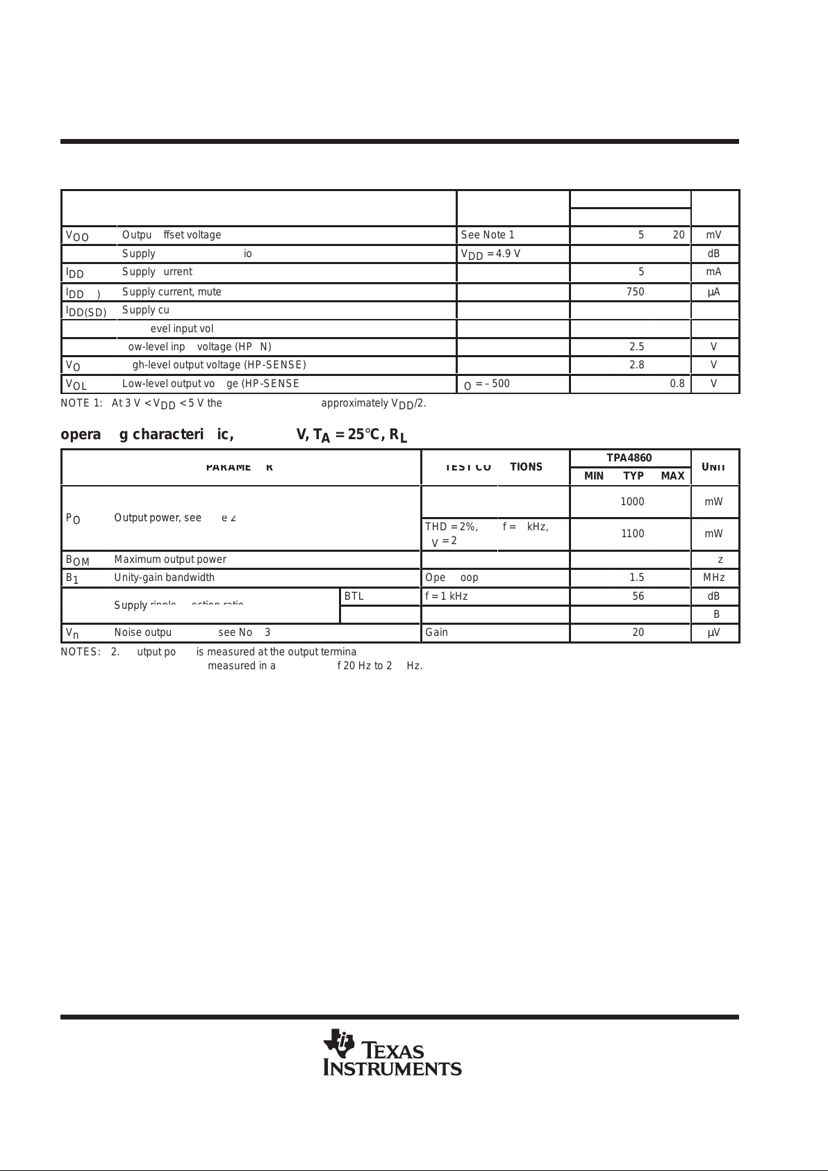
electrical characteristics at specified free-air temperature range, VDD = 5 V (unless otherwise
noted)
TPA4860
PARAMETER
TEST CONDITIONS
MIN TYP MAX
UNIT
V
OO
Output offset voltage
See Note 1
5
20
mV
Supply ripple rejection ratio
VDD = 4.9 V to 5.1 V
70
dB
I
DD
Supply current
3.5
mA
I
DD(M)
Supply current, mute
750
µA
I
DD(SD)
Supply current, shutdown
0.6
µA
V
IH
High-level input voltage (HP-IN)
2.5
V
V
IL
Low-level input voltage (HP-IN)
2.5
V
V
OH
High-level output voltage (HP-SENSE)
IO = 500 µA
2.5
2.8
V
V
OL
Low-level output voltage (HP-SENSE)
IO = –500 µA
0.2
0.8
V
NOTE 1: At 3 V < VDD < 5 V the dc output voltage is approximately VDD/2.
operating characteristic, VDD = 5 V, T
A
= 25°C, R
L
= 8 Ω
TPA4860
PARAMETER
TEST CONDITIONS
MIN TYP MAX
UNIT
ÁÁÁББББББББББББББ
Á
p
p
ÁÁ
Á
THD = 0.2%,
AV = 2
ÁÁÁ
Á
f = 1 kHz,
ÁÁÁ
Á
1000
ÁÁÁ
Á
mW
ÁÁ
Á
P
O
ББББББББББББББ
Á
Output power, see Note 2
ÁÁ
Á
THD = 2%,
AV = 2
ÁÁÁ
Á
f = 1 kHz,
ÁÁÁ
Á
1100
ÁÁÁ
Á
mW
B
OM
Maximum output power bandwidth
Gain = 10,
THD = 2%
20
kHz
B
1
Unity-gain bandwidth
Open Loop
1.5
MHz
pp
pp
BTL
f = 1 kHz
56
dB
Supply ripple rejection ratio
SE
f = 1 kHz
30
dB
V
n
Noise output voltage, see Note 3
Gain = 2
20
µV
NOTES: 2. Output power is measured at the output terminals of the device.
3. Noise voltage is measured in a bandwidth of 20 Hz to 20 kHz.
TPA4860
1-W MONO AUDIO POWER AMPLIFIER
SLOS164A – SEPTEMBER 1996 – REVISED MARCH 2000
5
POST OFFICE BOX 655303 • DALLAS, TEXAS 75265
TYPICAL CHARACTERISTICS
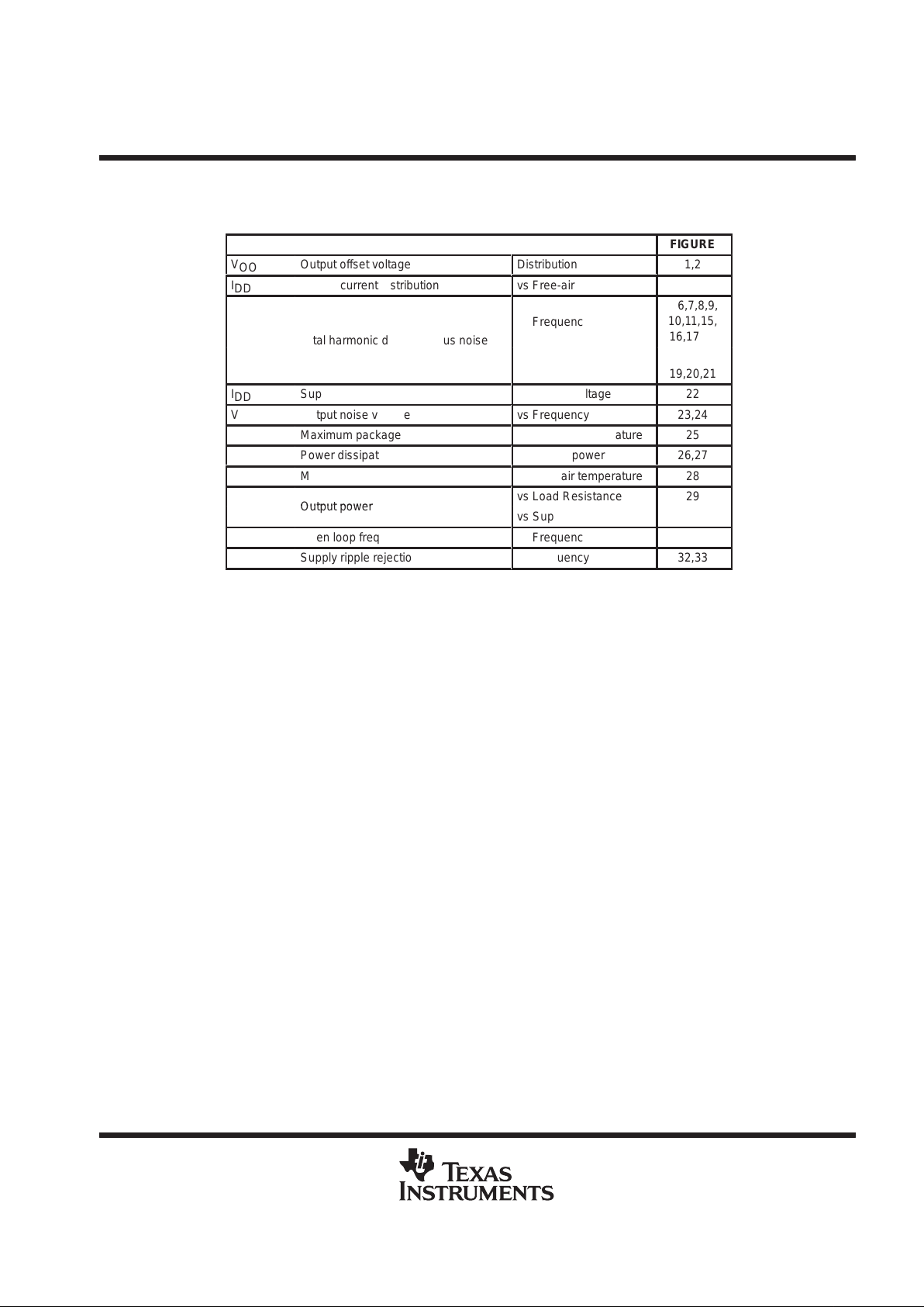
Table of Graphs
FIGURE
V
OO
Output offset voltage
Distribution
1,2
I
DD
Supply current distribution
vs Free-air temperature
3,4
ÁÁ
Á
THD+N
БББББББББ
Á
Total harmonic distortion plus noise
БББББ
Á
vs Frequency
ÁÁ
Á
5,6,7,8,9,
10,11,15,
16,17,18
ÁÁÁБББББББББÁБББББ
Á
vs Output power
ÁÁ
Á
12,13,14,
19,20,21
I
DD
Supply current
vs Supply voltage
22
V
n
Output noise voltage
vs Frequency
23,24
Maximum package power dissipation
vs Free-air temperature
25
Power dissipation
vs Output power
26,27
Maximum output power
vs Free-air temperature
28
p
p
vs Load Resistance
29
Output power
vs Supply Voltage
30
Open loop frequency response
vs Frequency
31
Supply ripple rejection ratio
vs Frequency
32,33
TPA4860
1-W MONO AUDIO POWER AMPLIFIER
SLOS164A – SEPTEMBER 1996 – REVISED MARCH 2000
6
POST OFFICE BOX 655303 • DALLAS, TEXAS 75265
TYPICAL CHARACTERISTICS
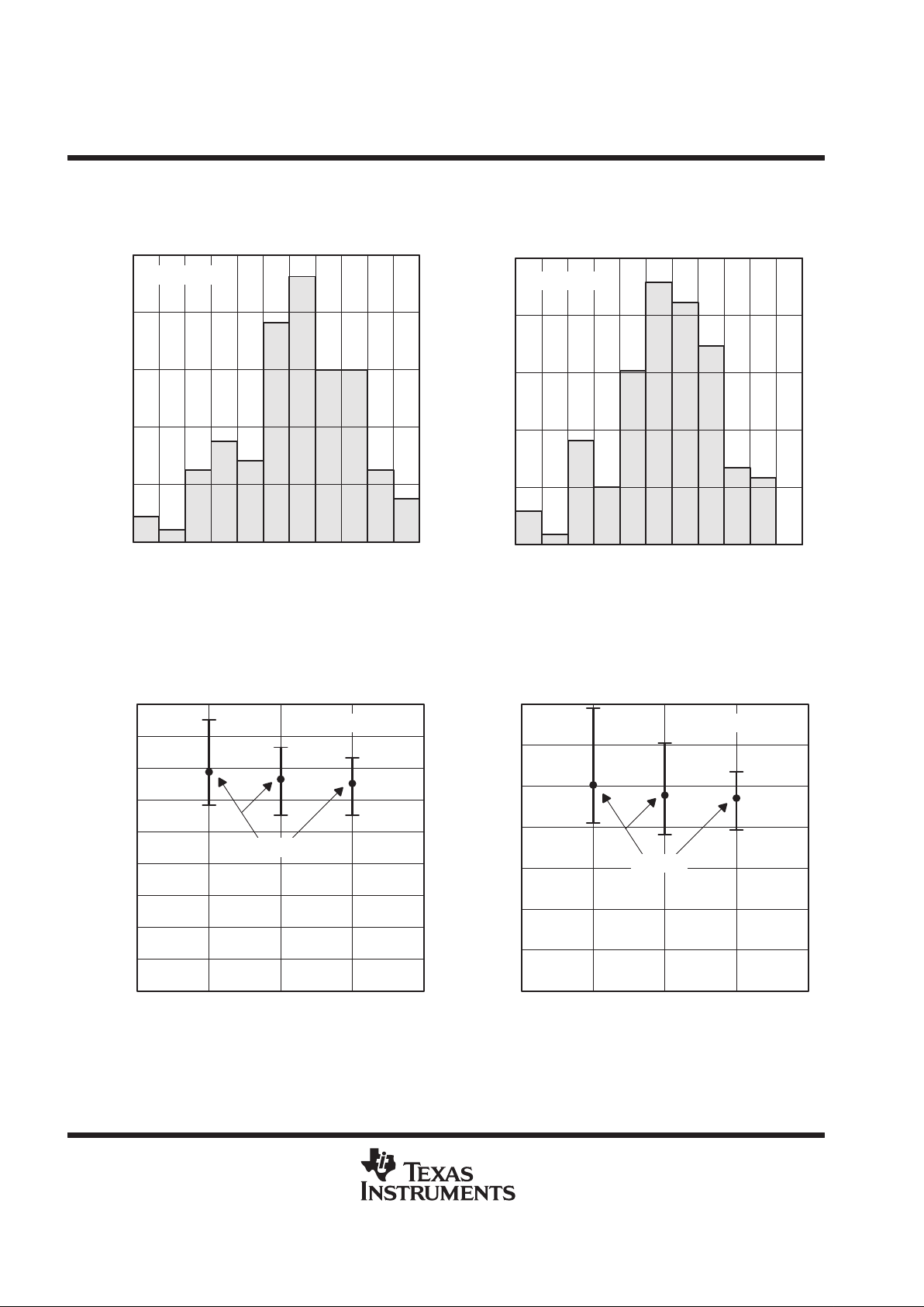
Figure 1
Number of Amplifiers
DISTRIBUTION OF TPA4860
OUTPUT OFFSET VOLTAGE
20
10
0
VOO – Output Offset Voltage – mV
25
15
5
VCC = 5 V
–3–2–101234567
Figure 2
Number of Amplifiers
DISTRIBUTION OF TPA4860
OUTPUT OFFSET VOLTAGE
20
10
0
VOO – Output Offset Voltage – mV
25
15
5
–3 –2 –1 0 1 2 3 4 5 6 7
VCC = 3.3 V
Figure 3
– Supply Current – mA
SUPPLY CURRENT DISTRIBUTION
vs
FREE-AIR TEMPERATURE
3.5
2
1
0
TA – Free-Air Temperature –°C
–20 25
2.5
1.5
0.5
VCC = 5 V
I
DD
3
85
4.5
4
Typical
Figure 4
– Supply Current – mA
SUPPLY CURRENT DISTRIBUTION
vs
FREE-AIR TEMPERATURE
3.5
2
1
0
TA – Free-Air Temperature –°C
–20 25
2.5
1.5
0.5
VCC = 3.3 V
I
DD
3
85
Typical
TPA4860
1-W MONO AUDIO POWER AMPLIFIER
SLOS164A – SEPTEMBER 1996 – REVISED MARCH 2000
7
POST OFFICE BOX 655303 • DALLAS, TEXAS 75265
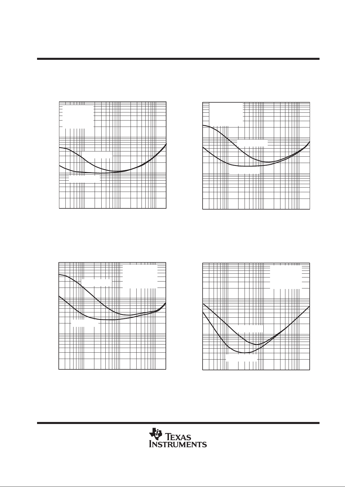
TYPICAL CHARACTERISTICS
Figure 5
TOTAL HARMONIC DISTORTION PLUS NOISE
vs
FREQUENCY
20
10
1
0.1
0.01
100 1 k 10 k 20 k
f – Frequency – Hz
VDD = 5 V
PO = 1 W
AV = –2 V/V
RL = 8 Ω
CB = 0.1 µF
CB = 1 µF
THD+N – Total Harmonic Distortion Plus Noise – %
Figure 6
TOTAL HARMONIC DISTORTION PLUS NOISE
vs
FREQUENCY
20
10
1
0.1
0.01
100 1 k 10 k 20 k
f – Frequency – Hz
VDD = 5 V
PO = 1 W
AV = –10 V/V
RL = 8 Ω
CB = 0.1 µF
CB = 1 µF
THD+N – Total Harmonic Distortion Plus Noise – %
Figure 7
TOTAL HARMONIC DISTORTION PLUS NOISE
vs
FREQUENCY
20
10
1
0.1
0.01
100 1 k 10 k 20 k
f – Frequency – Hz
VDD = 5 V
PO = 1 W
AV = –20 V/V
RL = 8 Ω
CB = 0.1 µF
CB = 1 µF
THD+N – Total Harmonic Distortion Plus Noise – %
Figure 8
TOTAL HARMONIC DISTORTION PLUS NOISE
vs
FREQUENCY
20
10
1
0.1
0.01
100 1 k 10 k 20 k
f – Frequency – Hz
VDD = 5 V
PO = 0.5 W
AV = –2 V/V
RL = 8 Ω
CB = 0.1 µF
CB = 1 µF
THD+N – Total Harmonic Distortion Plus Noise – %
TPA4860
1-W MONO AUDIO POWER AMPLIFIER
SLOS164A – SEPTEMBER 1996 – REVISED MARCH 2000
8
POST OFFICE BOX 655303 • DALLAS, TEXAS 75265
TYPICAL CHARACTERISTICS
Figure 9
TOTAL HARMONIC DISTORTION PLUS NOISE
vs
FREQUENCY
20
10
1
0.1
0.01
100 1 k 10 k 20 k
f – Frequency – Hz
VDD = 5 V
PO = 0.5 W
AV = –10 V/V
RL = 8 Ω
CB = 0.1 µF
CB = 1 µF
THD+N – Total Harmonic Distortion Plus Noise – %
Figure 10
TOTAL HARMONIC DISTORTION PLUS NOISE
vs
FREQUENCY
20
10
1
0.1
0.01
100 1 k 10 k 20 k
f – Frequency – Hz
THD+N – Total Harmonic Distortion Plus Noise – %
VDD = 5 V
PO = 0.5 W
AV = –20 V/V
RL = 8 Ω
CB = 0.1 µF
CB = 1 µF
Figure 11
TOTAL HARMONIC DISTORTION PLUS NOISE
vs
FREQUENCY
20
10
1
0.1
0.01
100 1 k 10 k 20 k
f – Frequency – Hz
THD+N – Total Harmonic Distortion Plus Noise – %
VDD = 5 V
AV = –10 V/V
Single Ended
RL = 8 Ω
PO = 250 mW
RL = 32 Ω
PO = 60 mW
Figure 12
TOTAL HARMONIC DISTORTION PLUS NOISE
vs
OUTPUT POWER
0.02
10
1
0.1
0.01
0.1 1
PO – Output Power – W
THD+N – Total Harmonic Distortion Plus Noise – %
VDD = 5 V
AV = –2 V/V
RL = 8 Ω
f = 20 Hz
CB = 0.1 µF
2
CB = 1 µF

TPA4860
1-W MONO AUDIO POWER AMPLIFIER
SLOS164A – SEPTEMBER 1996 – REVISED MARCH 2000
9
POST OFFICE BOX 655303 • DALLAS, TEXAS 75265
TYPICAL CHARACTERISTICS
Figure 13
TOTAL HARMONIC DISTORTION PLUS NOISE
vs
OUTPUT POWER
0.02
10
1
0.1
0.01
0.1 1
PO – Output Power – W
THD+N – Total Harmonic Distortion Plus Noise – %
VDD = 5 V
AV = –2 V/V
RL = 8 Ω
f = 1 kHz
2
CB = 0.1 µF
Figure 14
TOTAL HARMONIC DISTORTION PLUS NOISE
vs
OUTPUT POWER
0.02
10
1
0.1
0.01
0.1 1
PO – Output Power – W
THD+N – Total Harmonic Distortion Plus Noise – %
VDD = 5 V
AV = –2 V/V
RL = 8 Ω
f = 20 kHz
CB = 0.1 µF
2
Figure 15
TOTAL HARMONIC DISTORTION PLUS NOISE
vs
FREQUENCY
20
10
1
0.1
0.01
100 1 k 10 k 20 k
f – Frequency – Hz
THD+N – Total Harmonic Distortion Plus Noise – %
CB = 1 µF
VDD = 3.3 V
PO = 350 mW
RL = 8 Ω
AV = –2 V/V
CB = 0.1 µF
Figure 16
TOTAL HARMONIC DISTORTION PLUS NOISE
vs
FREQUENCY
20
10
1
0.1
0.01
100 1 k 10 k 20 k
f – Frequency – Hz
THD+N – Total Harmonic Distortion Plus Noise – %
CB = 1 µF
VDD = 3.3 V
PO = 350 mW
RL = 8 Ω
AV = –10 V/V
CB = 0.1 µF
TPA4860
1-W MONO AUDIO POWER AMPLIFIER
SLOS164A – SEPTEMBER 1996 – REVISED MARCH 2000
10
POST OFFICE BOX 655303 • DALLAS, TEXAS 75265
TYPICAL CHARACTERISTICS
Figure 17
TOTAL HARMONIC DISTORTION PLUS NOISE
vs
FREQUENCY
20
10
1
0.1
0.01
100 1 k 10 k 20 k
f – Frequency – Hz
THD+N – Total Harmonic Distortion Plus Noise – %
VDD = 3.3 V
PO = 350 mW
RL = 8 Ω
AV = –20 V/V
CB = 1 µF
CB = 0.1 µF
Figure 18
TOTAL HARMONIC DISTORTION PLUS NOISE
vs
FREQUENCY
20
10
1
0.1
0.01
100 1 k 10 k 20 k
f – Frequency – Hz
THD+N – Total Harmonic Distortion Plus Noise – %
VDD = 3.3 V
AV = –10 V/V
Single Ended
RL = 32 Ω
PO = 60 mW
RL = 8 Ω
PO = 250 mW
Figure 19
TOTAL HARMONIC DISTORTION PLUS NOISE
vs
OUTPUT POWER
0.02
10
1
0.1
0.01
0.1 1
PO – Output Power – W
THD+N – Total Harmonic Distortion Plus Noise – %
VDD = 3.3 V
AV = –2 V/V
RL = 8 Ω
f = 20 Hz
CB = 0.1 µF
2
CB = 1.0 µF
Figure 20
TOTAL HARMONIC DISTORTION PLUS NOISE
vs
OUTPUT POWER
0.02
10
1
0.1
0.01
0.1 1
PO – Output Power – W
THD+N – Total Harmonic Distortion Plus Noise – %
VDD = 3.3 V
AV = –2 V/V
RL = 8 Ω
f = 1 kHz
CB = 0.1 µF
2

TPA4860
1-W MONO AUDIO POWER AMPLIFIER
SLOS164A – SEPTEMBER 1996 – REVISED MARCH 2000
11
POST OFFICE BOX 655303 • DALLAS, TEXAS 75265
TYPICAL CHARACTERISTICS
Figure 21
TOTAL HARMONIC DISTORTION PLUS NOISE
vs
OUTPUT POWER
20 m
10
1
0.1
0.01
0.1 1
PO – Output Power – W
THD+N – Total Harmonic Distortion Plus Noise – %
VDD = 3.3 V
AV = –2 V/V
RL = 8 Ω
f = 20 kHz
CB = 0.1 µF
2
Figure 22
– Supplu Current – mAI
DD
SUPPLY CURRENT
vs
SUPPLY VOLTAGE
2.5
5
2
1
0
3 3.5
VDD – Supply Voltage – V
4 4.5 5 5.5
4
3
TA = 0°C
TA = 85°C
TA = 25°C
TA = –20°C
Figure 23
OUTPUT NOISE VOLTAGE
vs
FREQUENCY
20
10
3
10
2
10
1
1
100 1 k 10 k 20 k
f – Frequency – Hz
VCC = 5 V
V01 +V02
V01
V02
– Output Noise Voltage – V
n
Vµ
Figure 24
OUTPUT NOISE VOLTAGE
vs
FREQUENCY
20
10
3
10
2
10
1
1
100 1 k 10 k 20 k
f – Frequency – Hz
VCC = 3.3 V
V02
V01
V01 +V02
– Output Noise Voltage – V
n
Vµ
TPA4860
1-W MONO AUDIO POWER AMPLIFIER
SLOS164A – SEPTEMBER 1996 – REVISED MARCH 2000
12
POST OFFICE BOX 655303 • DALLAS, TEXAS 75265
TYPICAL CHARACTERISTICS
Figure 25
Maximum Package Power Dissipation – W
MAXIMUM PACKAGE POWER DISSIPATION
vs
FREE-AIR TEMPERATURE
–25
1.5
1
0.5
0
0 75 175
TA – Free-Air Temperature – °C
25 50 100 125 150
1.25
0.75
0.25
Figure 26
Power Dissipation – W
POWER DISSIPATION
vs
OUTPUT POWER
1.5
1
0.5
0
0 0.75 1.75
PO – Output Power – W
0.25 0.5 1 1.25 1.5
VDD = 5 V
RL = 4 Ω
RL = 8 Ω
RL = 16 Ω
Figure 27
POWER DISSIPATION
vs
OUTPUT POWER
1
0.5
0.25
0
0 0.75
PO – Output Power – W
0.25 0.5
VDD = 3.3 V
RL = 4 Ω
RL = 8 Ω
RL = 16 Ω
0.75
Power Dissipation – W
Figure 28
160
40
20
0
0 0.25 1.500.5 0.75 1
RL = 16 Ω
– Free-Air Temperature –
PO – Maximum Output Power – W
1.25
RL = 8 Ω
RL = 4 Ω
C
°
T
A
80
60
120
100
140
MAXIMUM OUTPUT POWER
vs
FREE-AIR TEMPERATURE
TPA4860
1-W MONO AUDIO POWER AMPLIFIER
SLOS164A – SEPTEMBER 1996 – REVISED MARCH 2000
13
POST OFFICE BOX 655303 • DALLAS, TEXAS 75265
TYPICAL CHARACTERISTICS
Figure 29
– Power Output – W
OUTPUT POWER
vs
LOAD RESISTANCE
4
1.4
0.8
0.4
0
820 36
Load Resistance – Ω
12 16 24 28 32
1
0.6
0.2
VCC = 5 V
VCC = 3.3 V
P
O
AV = –2 V/V
f = 1 kHz
CB = 0.1 µF
THD+n ≤ 1%
1.2
4840 44
Figure 30
– Power Output – W
OUTPUT POWER
vs
SUPPLY VOLTAGE
3
1.75
1
0.5
0
3.5 5
Supply Voltage – V
4 4.5 5.5
1.25
0.75
0.25
P
O
1.5
AV = –2 V/V
f = 1 kHz
CB = 0.1 µF
THD+n ≤ 1%
2.5
2
RL = 8 Ω
RL = 4 Ω
RL = 16 Ω
Figure 31
G – Gain – dB
OPEN LOOP FREQUENCY RESPONSE
10
100
60
20
–20
100 100 k
f – Frequency – Hz
VDD = 5 V
RL = 8 Ω
CB = 0.1 µF
1 k 10 k 1 M 10 M
80
40
0
45°
–45°
–135°
–225°
0°
–90°
–180°
Phase
Gain
Phase
Figure 32
SUPPLY RIPPLE REJECTION RATIO
vs
FREQUENCY
100
0
–90
–100
1 k 10 k 20 k
f – Frequency – Hz
VDD = 5 V
RL = 8 Ω
Bridge Tied
Load
CB = 0.1 µF
CB = 1 µF
–80
–70
–60
–50
–40
–30
–20
–10
Supply Ripple Rejection Ratio – dB

TPA4860
1-W MONO AUDIO POWER AMPLIFIER
SLOS164A – SEPTEMBER 1996 – REVISED MARCH 2000
14
POST OFFICE BOX 655303 • DALLAS, TEXAS 75265
TYPICAL CHARACTERISTICS
SUPPLY RIPPLE REJECTION RATIO
vs
FREQUENCY
100
0
–90
–100
1 k 10 k 20 k
f – Frequency – Hz
CB = 0.1 µF
CB = 1 µF
–80
–70
–60
–50
–40
–30
–20
–10
VDD = 5 V
RL = 8 Ω
Single Ended
Figure 33
Supply Ripple Rejection Ratio – dB
APPLICATION INFORMATION
bridged-tied load versus single-ended mode
Figure 34 shows a linear audio power amplifier (AP A) in a bridge tied load (BTL) configuration. A BTL amplifier
actually consists of two linear amplifiers driving both ends of the load. There are several potential benefits to
this differential drive configuration but initially let us consider power to the load. The differential drive to the
speaker means that as one side is slewing up the other side is slewing down and vice versa. This in effect
doubles the voltage swing on the load as compared to a ground referenced load. Plugging twice the voltage
into the power equation, where voltage is squared, yields 4 times the output power from the same supply rail
and load impedance (see equation 1).
Power
+
V
(rms)
2
R
L
(1)
V
(rms)
+
V
O(PP)
22
Ǹ

TPA4860
1-W MONO AUDIO POWER AMPLIFIER
SLOS164A – SEPTEMBER 1996 – REVISED MARCH 2000
15
POST OFFICE BOX 655303 • DALLAS, TEXAS 75265
APPLICATION INFORMATION
bridged-tied load versus single-ended mode (continued)
R
L
2x V
O(PP)
V
O(PP)
–V
O(PP)
V
DD
V
DD
Figure 34. Bridge-Tied Load Configuration
In a typical computer sound channel operating at 5 V, bridging raises the power into a 8-Ω speaker from a
singled-ended (SE) limit of 250 mW to 1 W. In sound power , that is a 6-dB improvement which is loudness that
can be heard. In addition to increased power there are frequency response concerns, consider the single-supply
SE configuration shown in Figure 35. A coupling capacitor is required to block the dc offset voltage from reaching
the load. These capacitors can be quite large (approximately 40 µF to 1000 µF) so they tend to be expensive,
occupy valuable PCB area, and have the additional drawback of limiting low-frequency performance of the
system. This frequency limiting effect is due to the high pass filter network created with the speaker impedance
and the coupling capacitance and is calculated with equation 2.
f
c
+
1
2pR
L
C
C
(2)
For example, a 68-µF capacitor with an 8-Ω speaker would attenuate low frequencies below 293 Hz. The BTL
configuration cancels the dc offsets, which eliminates the need for the blocking capacitors. Low-frequency
performance is then limited only by the input network and speaker response. Cost and PCB space are also
minimized by eliminating the bulky coupling capacitor.
R
L
C
C
V
O(PP)
V
O(PP)
V
DD
Figure 35. Single-Ended Configuration

TPA4860
1-W MONO AUDIO POWER AMPLIFIER
SLOS164A – SEPTEMBER 1996 – REVISED MARCH 2000
16
POST OFFICE BOX 655303 • DALLAS, TEXAS 75265
APPLICATION INFORMATION
bridged-tied load versus single-ended mode (continued)
Increasing power to the load does carry a penalty of increased internal power dissipation. The increased
dissipation is understandable considering that the BTL configuration produces 4 times the output power of the
SE configuration. Internal dissipation versus output power is discussed further in the
thermal considerations
section.
BTL amplifier efficiency
Linear amplifiers are notoriously inefficient. The primary cause of these inefficiencies is voltage drop across the
output stage transistors. There are two components of the internal voltage drop. One is the headroom or dc
voltage drop that varies inversely to output power. The second component is due to the sinewave nature of the
output. The total voltage drop can be calculated by subtracting the RMS value of the output voltage from V
DD
.
The internal voltage drop multiplied by the RMS value of the supply current, IDDrms, determines the internal
power dissipation of the amplifier.
An easy to use equation to calculate efficiency starts out as being equal to the ratio of power from the power
supply to the power delivered to the load. To accurately calculate the RMS values of power in the load and in
the amplifier, the current and voltage waveform shapes must first be understood (see Figure 36).
V
(LRMS)
V
O
I
DD
I
DD(RMS)
Figure 36. Voltage and Current Waveforms for BTL Amplifiers
Although the voltages and currents for SE and BTL are sinusoidal in the load, currents from the supply are very
different between SE and BTL configurations. In an SE application the current waveform is a half-wave rectified
shape, whereas in BTL it is a full-wave rectified waveform. This means RMS conversion factors are different.
Keep in mind that for most of the waveform both the push and pull transistor are not on at the same time, which
supports the fact that each amplifier in the BTL device only draws current from the supply for half the waveform.
The following equations are the basis for calculating amplifier efficiency.

TPA4860
1-W MONO AUDIO POWER AMPLIFIER
SLOS164A – SEPTEMBER 1996 – REVISED MARCH 2000
17
POST OFFICE BOX 655303 • DALLAS, TEXAS 75265
APPLICATION INFORMATION
VLrms
+
V
P
2
Ǹ
IDDrms
+
2V
P
p
R
L
P
SUP
+
VDDIDDrms
+
VDD2V
P
p
R
L
Efficiency
+
P
L
P
SUP
Efficiency of a BTL Configuration
+
p
V
P
2V
DD
+
p
ǒ
PLR
L
2
Ǔ
1ń2
2V
DD
(3)
PL+
V
L
rms
2
R
L
+
V
p
2
2R
L
Where:
(4)
NO TAG employs equation 4 to calculate efficiencies for four different output power levels. Note that the
efficiency of the amplifier is quite low for lower power levels and rises sharply as power to the load is increased,
resulting in a nearly flat internal power dissipation over the normal operating range. Note that the internal
dissipation at full output power is less than in the half power range. Calculating the efficiency for a specific
system is the key to proper power supply design. For a stereo 1-W audio system with 8-Ω loads and a 5-V supply ,
the maximum draw on the power supply is almost 3.25 W.
Table 1. Efficiency vs Output Power in 5-V 8-Ω BTL Systems
OUTPUT POWER
(W)
EFFICIENCY
(%)
PEAK-TO-PEAK
VOLTAGE
(V)
INTERNAL
DISSIPATION
(W)
0.25 31.4 2.00 0.55
0.50 44.4 2.83 0.62
1.00 62.8 4.00 0.59
1.25 70.2 4.47
†
0.53
†
High peak voltages cause the THD to increase.
A final point to remember about linear amplifiers whether they are SE or BTL configured is how to manipulate
the terms in the efficiency equation to utmost advantage when possible. Note that in equation 4, VDD is in the
denominator. This indicates that as VDD goes down, efficiency goes up.
For example, if the 5-V supply is replaced with a 10-V supply (TPA4860 has a maximum recommended V
DD
of 5.5 V) in the calculations of NO T AG then ef ficiency at 1 W would fall to 31% and internal power dissipation
would rise to 2.18 W from 0.59 W at 5 V . Then for a stereo 1-W system from a 10-V supply , the maximum draw
would be almost 6.5 W. Choose the correct supply voltage and speaker impedance for the application.

TPA4860
1-W MONO AUDIO POWER AMPLIFIER
SLOS164A – SEPTEMBER 1996 – REVISED MARCH 2000
18
POST OFFICE BOX 655303 • DALLAS, TEXAS 75265
APPLICATION INFORMATION
selection of components
Figure 37 is a schematic diagram of a typical notebook computer application circuit.
Audio
Input
Bias
Control
VDD = 5 V
1 W
Internal
Speaker
12
10
15
1, 4, 8, 9, 16
VO1
VO2
V
DD
2
3
7
6
5
14
13
11 GAIN
IN+
IN–
BYPASS
HP-IN1
HP-IN2
HP-SENSE
SHUTDOWN
VDD/2
C
I
R
I
R
F
V
DD
R
PU
Headphone
Plug
NC
C
F
50 kΩ 50 kΩ
46 kΩ
46 kΩ
C
B
C
S
Figure 37. TPA4860 Typical Notebook Computer Application Circuit
gain setting resistors, RF and R
I
The gain for the TPA4860 is set by resistors RF and RI according to equation 5.
(5)
Gain
+*2
ǒ
R
F
R
I
Ǔ
BTL mode operation brings about the factor of 2 in the gain equation due to the inverting amplifier mirroring the
voltage swing across the load. Given that the TPA4860 is a MOS amplifier, the input impedance is very high,
consequently input leakage currents are not generally a concern although noise in the circuit increases as the
value of R
F
increases. In addition, a certain range of RF values is required for proper startup operation of the
amplifier. Taken together it is recommended that the effective impedance seen by the inverting node of the
amplifier be set between 5 kΩ and 20 kΩ. The effective impedance is calculated in equation 6.
(6)
Effective Impedance
+
RFR
I
RF)
R
I
As an example, consider an input resistance of 10 kΩ and a feedback resistor of 50 kΩ. The gain of the amplifier
would be –10 and the effective impedance at the inverting terminal would be 8.3 kΩ, which is well within the
recommended range.

TPA4860
1-W MONO AUDIO POWER AMPLIFIER
SLOS164A – SEPTEMBER 1996 – REVISED MARCH 2000
19
POST OFFICE BOX 655303 • DALLAS, TEXAS 75265
APPLICATION INFORMATION
gain setting resistors, RF and RI (continued)
For high performance applications metal film resistors are recommended because they tend to have lower noise
levels than carbon resistors. For values of RF above 50 kΩ the amplifier tends to become unstable due to a pole
formed from RF and the inherent input capacitance of the MOS input structure. For this reason, a small
compensation capacitor of approximately 5 pF should be placed in parallel with R
F
. This, in effect, creates a low
pass filter network with the cutoff frequency defined in equation 7.
(7)
f
c(lowpass)
+
1
2pR
FCF
For example, if RF is 100 kΩ and Cf is 5 pF then fc is 318 kHz, which is well outside of the audio range.
input capacitor, C
I
In the typical application an input capacitor, CI, is required to allow the amplifier to bias the input signal to the
proper dc level for optimum operation. In this case, CI and RI form a high-pass filter with the corner frequency
determined in equation 8.
(8)
f
c(highpass)
+
1
2pR
I
C
I
The value of CI is important to consider as it directly affects the bass (low frequency) performance of the circuit.
Consider the example where R
I
is 10 kΩ and the specification calls for a flat bass response down to 40 Hz.
Equation 8 is reconfigured as equation 9.
(9)
CI+
1
2pR
I
f
c
In this example, CI is 0.40 µF, so one would likely choose a value in the range of 0.47 µF to 1 µF. A further
consideration for this capacitor is the leakage path from the input source through the input network (RI, CI) and
the feedback resistor (RF) to the load. This leakage current creates a dc offset voltage at the input to the amplifier
that reduces useful headroom, especially in high gain applications. For this reason a low-leakage tantalum or
ceramic capacitor is the best choice. When polarized capacitors are used, the positive side of the capacitor
should face the amplifier input in most applications as the dc level there is held at V
DD
/2, which is likely higher
that the source dc level. Note that it is important to confirm the capacitor polarity in the application.
power supply decoupling, C
S
The TPA4860 is a high-performance CMOS audio amplifier that requires adequate power supply decoupling
to ensure the output total harmonic distortion (THD) is as low as possible. Power supply decoupling also
prevents oscillations for long lead lengths between the amplifier and the speaker. The optimum decoupling is
achieved by using two capacitors of different types that target different types of noise on the power supply leads.
For higher frequency transients, spikes, or digital hash on the line, a good low equivalent-series-resistance
(ESR) ceramic capacitor, typically 0.1 µF placed as close as possible to the device V
DD
lead, works best. For
filtering lower-frequency noise signals, a larger aluminum electrolytic capacitor of 10 µF or greater placed near
the power amplifier is recommended.

TPA4860
1-W MONO AUDIO POWER AMPLIFIER
SLOS164A – SEPTEMBER 1996 – REVISED MARCH 2000
20
POST OFFICE BOX 655303 • DALLAS, TEXAS 75265
APPLICATION INFORMATION
midrail bypass capacitor, C
B
The midrail bypass capacitor, CB, serves several important functions. During start-up or recovery from
shutdown mode, CB determines the rate at which the amplifier starts up. This helps to push the start-up pop
noise into the subaudible range (so low it can not be heard). The second function is to reduce noise produced
by the power supply caused by coupling into the output drive signal. This noise is from the midrail generation
circuit internal to the amplifier. The capacitor is fed from a 25-kΩ source inside the amplifier . T o keep the start-up
pop as low as possible, the relationship shown in equation 10 should be maintained.
(10)
1
ǒ
CB
25 kΩ
Ǔ
v
1
ǒ
CIR
I
Ǔ
As an example, consider a circuit where CB is 0.1 µF, CI is 0.22 µF and RI is 10 kΩ. Inserting these values into
the equation 9 we get: 400 ≤ 454 which satisfies the rule. Bypass capacitor, CB, values of 0.1 µF to 1 µF ceramic
or tantalum low-ESR capacitors are recommended for the best THD and noise performance.
single-ended operation
Figure 38 is a schematic diagram of the recommended SE configuration. In SE mode configurations, the load
should be driven from the primary amplifier output (OUT1, terminal 10).
Audio
Input
VDD = 5 V
250-mW
External
Speaker
12
10
15
VO1
VO2
V
DD
5
14
13
11 GAIN
IN+
IN–
BYPASS
VDD/2
C
I
R
I
R
F
CSE = 0.1 µF
RSE = 50 Ω
C
C
C
B
C
S
Figure 38. Singled-Ended Mode
Gain is set by the RF and RI resistors and is shown in equation 1 1. Since the inverting amplifier is not used to
mirror the voltage swing on the load, the factor of 2 is not included.
(11)
Gain
+*
ǒ
R
F
R
I
Ǔ
The phase margin of the inverting amplifier into an open circuit is not adequate to ensure stability, so a
termination load should be connected to VO2. This consists of a 50-Ω resistor in series with a 0.1-µF capacitor
to ground. It is important to avoid oscillation of the inverting output to minimize noise and power dissipation.

TPA4860
1-W MONO AUDIO POWER AMPLIFIER
SLOS164A – SEPTEMBER 1996 – REVISED MARCH 2000
21
POST OFFICE BOX 655303 • DALLAS, TEXAS 75265
APPLICATION INFORMATION
single-ended operation (continued)
The output coupling capacitor required in single-supply SE mode also places additional constraints on the
selection of other components in the amplifier circuit. The rules described earlier still hold with the addition of
the following relationship:
(12)
1
ǒ
CB
25 kΩ
Ǔ
v
1
ǒ
CIR
I
Ǔ
Ơ
1
R
L
C
C
output coupling capacitor, C
C
In the typical single-supply SE configuration, an output coupling capacitor (CC) is required to block the dc bias
at the output of the amplifier thus preventing dc currents in the load. As with the input coupling capacitor, the
output coupling capacitor and impedance of the load form a high-pass filter governed by equation 13.
(13)
f
chigh
+
1
2pR
L
C
C
The main disadvantage, from a performance standpoint, is that the load impedances are typically small, which
drives the low-frequency corner higher. Large values of CC are required to pass low frequencies into the load.
Consider the example where a C
C
of 68 µF is chosen and loads vary from 8 Ω, 32 Ω, to 47 kΩ. Table 2
summarizes the frequency response characteristics of each configuration.
Table 2. Common Load Impedances vs Low Frequency Output Characteristics in SE Mode
R
L
C
C
LOWEST FREQUENCY
8 Ω 68 µF 293 Hz
32 Ω 68 µF
73 Hz
47,000 Ω 68 µF 0.05 Hz
As Table 2 indicates, most of the bass response is attenuated into 8-Ω loads while headphone response is
adequate and drive into line level inputs (a home stereo for example) is very good.
headphone sense circuitry, R
pu
The TP A4860 is commonly used in systems where there is an internal speaker and a jack for driving external
loads (i.e., headphones). In these applications, it is usually desirable to mute the internal speaker(s) when the
external load is in use. The headphone inputs (HP-1, HP-2) and headphone output (HP-SENSE) of the TP A4860
were specifically designed for this purpose. Many standard headphone jacks are available with an internal
single-pole single-throw (SPST) switch that makes or breaks a circuit when the headphone plug is inserted.
Asserting either or both HP-1 and/or HP-2 high mutes the output stage of the amplifier and causes HP-SENSE
to go high. In battery-powered applications where power conservation is critical HP-SENSE can be connected
to the shutdown input as shown in Figure 39. This places the amplifier in a very low current state for maximum
power savings. Pullup resistors in the range from 1 kΩ to 10 kΩ are recommended for 5-V and 3.3-V operation.

TPA4860
1-W MONO AUDIO POWER AMPLIFIER
SLOS164A – SEPTEMBER 1996 – REVISED MARCH 2000
22
POST OFFICE BOX 655303 • DALLAS, TEXAS 75265
APPLICATION INFORMATION
Bias
Control
2
3
7
6
HP-IN1
HP-IN2
HP-SENSE
SHUTDOWN
V
DD
R
PU
Headphone
Plug
NC
Figure 39. Schematic Diagram of Typical Headphone Sense Application
Table 3 details the logic for the mute function of the TPA4860.
Table 3. Truth Table for Headphone Sense and Shutdown Functions
INPUTS
†
OUTPUT
AMPLIFIER
HP-1 HP-2 SHUTDOWN HP-SENSE
STATE
Low Low Low Low Active
Low High Low High Mute
High Low Low High Mute
High High Low High Mute
X X High X Shutdown
†
Inputs should never be left unconnected.
X = do not care
shutdown mode
The TP A4860 employs a shutdown mode of operation designed to reduce quiescent supply current, I
DD(q)
, to
the absolute minimum level during periods of nonuse for battery-power conservation. For example, during
device sleep modes or when other audio-drive currents are used (i.e., headphone mode), the speaker drive is
not required. The SHUTDOWN input terminal should be held low during normal operation when the amplifier
is in use. Pulling SHUTDOWN high causes the outputs to mute and the amplifier to enter a low-current state,
I
DD
<1 µA. SHUTDOWN should never be left unconnected because amplifier operation would be unpredictable.
using low-ESR capacitors
Low-ESR capacitors are recommended throughout this applications section. A real capacitor can be modeled
simply as a resistor in series with an ideal capacitor. The voltage drop across this resistor minimizes the
beneficial effects of the capacitor in the circuit. The lower the equivalent value of this resistance the more the
real capacitor behaves like an ideal capacitor.
thermal considerations
A prime consideration when designing an audio amplifier circuit is internal power dissipation in the device. The
curve in Figure 40 provides an easy way to determine what output power can be expected out of the TP A4860
for a given system ambient temperature in designs using 5-V supplies. This curve assumes no forced airflow
or additional heat sinking.

TPA4860
1-W MONO AUDIO POWER AMPLIFIER
SLOS164A – SEPTEMBER 1996 – REVISED MARCH 2000
23
POST OFFICE BOX 655303 • DALLAS, TEXAS 75265
APPLICATION INFORMATION
160
40
20
0
0 0.25 1.500.5 0.75 1
RL = 16 Ω
– Free-Air Temperature –
Maximum Output Power – W
1.25
RL = 8 Ω
RL = 4 Ω
C
°
T
A
80
60
120
100
140
VDD = 5 V
Figure 40. Free-Air Temperature Versus Maximum Continuous Output Power
5-V versus 3.3-V operation
The TPA4860 was designed for operation over a supply range of 2.7 V to 5.5 V. This data sheet provides full
specifications for 5-V and 3.3-V operation, as these are considered to be the two most common standard
voltages. There are no special considerations for 3.3-V versus 5-V operation as far as supply bypassing, gain
setting, or stability. Supply current is slightly reduced from 3.5 mA (typical) to 2.5 mA (typical). The most
important consideration is that of output power. Each amplifier in TPA4860 can produce a maximum voltage
swing of V
DD
– 1 V . This means, for 3.3-V operation, clipping starts to occur when V
O(PP)
= 2.3 V as opposed
to when V
O(PP)
= 4 V while operating at 5 V . The reduced voltage swing subsequently reduces maximum output
power into an 8-Ω load to less than 0.33 W before distortion begins to become significant.
Operation at 3.3-V supplies, as can be shown from the efficiency formula in equation 4, consumes
approximately two-thirds the supply power for a given output-power level than operation from 5-V supplies.
When the application demands less than 500 mW, 3.3-V operation should be strongly considered, especially
in battery-powered applications.

TPA4860
1-W MONO AUDIO POWER AMPLIFIER
SLOS164A – SEPTEMBER 1996 – REVISED MARCH 2000
24
POST OFFICE BOX 655303 • DALLAS, TEXAS 75265
MECHANICAL INFORMATION
D (R-PDSO-G**) PLASTIC SMALL-OUTLINE PACKAGE
14 PINS SHOWN
4040047/D 10/96
0.228 (5,80)
0.244 (6,20)
0.069 (1,75) MAX
0.010 (0,25)
0.004 (0,10)
1
14
0.014 (0,35)
0.020 (0,51)
A
0.157 (4,00)
0.150 (3,81)
7
8
0.044 (1,12)
0.016 (0,40)
Seating Plane
0.010 (0,25)
PINS **
0.008 (0,20) NOM
A MIN
A MAX
DIM
Gage Plane
0.189
(4,80)
(5,00)
0.197
8
(8,55)
(8,75)
0.337
14
0.344
(9,80)
16
0.394
(10,00)
0.386
0.004 (0,10)
M
0.010 (0,25)
0.050 (1,27)
0°–8°
NOTES: A. All linear dimensions are in inches (millimeters).
B. This drawing is subject to change without notice.
C. Body dimensions do not include mold flash or protrusion, not to exceed 0.006 (0,15).
D. Falls within JEDEC MS-012

IMPORTANT NOTICE
T exas Instruments and its subsidiaries (TI) reserve the right to make changes to their products or to discontinue
any product or service without notice, and advise customers to obtain the latest version of relevant information
to verify, before placing orders, that information being relied on is current and complete. All products are sold
subject to the terms and conditions of sale supplied at the time of order acknowledgement, including those
pertaining to warranty, patent infringement, and limitation of liability.
TI warrants performance of its semiconductor products to the specifications applicable at the time of sale in
accordance with TI’s standard warranty. Testing and other quality control techniques are utilized to the extent
TI deems necessary to support this warranty. Specific testing of all parameters of each device is not necessarily
performed, except those mandated by government requirements.
CERT AIN APPLICATIONS USING SEMICONDUCTOR PRODUCTS MAY INVOLVE POTENTIAL RISKS OF
DEATH, PERSONAL INJURY, OR SEVERE PROPERTY OR ENVIRONMENTAL DAMAGE (“CRITICAL
APPLICATIONS”). TI SEMICONDUCTOR PRODUCTS ARE NOT DESIGNED, AUTHORIZED, OR
WARRANTED TO BE SUITABLE FOR USE IN LIFE-SUPPORT DEVICES OR SYSTEMS OR OTHER
CRITICAL APPLICATIONS. INCLUSION OF TI PRODUCTS IN SUCH APPLICA TIONS IS UNDERSTOOD T O
BE FULLY AT THE CUSTOMER’S RISK.
In order to minimize risks associated with the customer’s applications, adequate design and operating
safeguards must be provided by the customer to minimize inherent or procedural hazards.
TI assumes no liability for applications assistance or customer product design. TI does not warrant or represent
that any license, either express or implied, is granted under any patent right, copyright, mask work right, or other
intellectual property right of TI covering or relating to any combination, machine, or process in which such
semiconductor products or services might be or are used. TI’s publication of information regarding any third
party’s products or services does not constitute TI’s approval, warranty or endorsement thereof.
Copyright 2000, Texas Instruments Incorporated
 Loading...