

20
19
18
17
16
15
14
13
12
11
10
9
8
7
6
5
4
3
2
1
TPA4411RTJ
INR
INL
PGND
OUTL PVSSSVSS
C1N
PVDDSGND
A1
B1
C1
D1
A2
A3 A4
SDL
SVDD
C1P
SDR
NC
NC
OUTR
TPA4411YZH
20
19
18
17
16
15
14
13
12
11
10
9
8
7
6
5
4
3
2
1
TPA4411MRTJ
TPA4411
TPA4411M
www.ti.com
80-mW DIRECTPATH™ STEREO HEADPHONE DRIVER
1
FEATURES
2
• Space Saving Packages
– 20-Pin, 4 mm × 4 mm Thin QFN
– TPA4411 – Thermally Optimized
PowerPAD™ Package
– TPA4411M – Thermally Enhanced
PowerPAD™ Package
– 16-Ball, 2.18 mm × 2.18 mm WCSP
• Ground-Referenced Outputs Eliminate
DC-Bias Voltages on Headphone Ground Pin
– No Output DC-Blocking Capacitors
– Reduced Board Area
– Reduced Component Cost
– Improved THD+N Performance
– No Degradation of Low-Frequency
Response Due to Output Capacitors
• Wide Power Supply Range: 1.8 V to 4.5 V
• 80-mW/Ch Output Power into 16- Ω at 4.5 V
• Independent Right and Left Channel
Shutdown Control
• Short-Circuit and Thermal Protection
• Pop Reduction Circuitry
APPLICATIONS
• Notebook Computers
• CD / MP3 Players
• Smart Phones
• Cellular Phones
• PDAs
SLOS430E – AUGUST 2004 – REVISED MARCH 2008
DESCRIPTION
The TPA4411 and TPA4411M are stereo headphone
drivers designed to allow the removal of the output
DC-blocking capacitors for reduced component count
and cost. The TPA4411 and TPA4411M are ideal for
small portable electronics where size and cost are
critical design parameters.
The TPA4411 and TPA4411M are capable of driving
80 mW into a 16- Ω load at 4.5 V. Both TPA4411 and
TPA4411M have a fixed gain of – 1.5 V/V and
headphone outputs that have ± 8-kV IEC ESD
protection. The TPA4411 and TPA4411M have
independent shutdown control for the right and left
audio channels.
The TPA4411 is available in a 2.18 mm × 2.18 mm
WCSP and 4 mm × 4 mm Thin QFN packages. The
TPA4411M is available in a 4 mm × 4 mm Thin QFN
package. The TPA4411RTJ package is a thermally
optimized PowerPAD™ package allowing the
maximum amount of thermal dissipation and the
TPA4411MRTJ is a thermally enhanced PowerPAD
package designed to match competitive package
footprints.
1
Please be aware that an important notice concerning availability, standard warranty, and use in critical applications of
Texas Instruments semiconductor products and disclaimers thereto appears at the end of this data sheet.
2 PowerPAD, DirectPath are trademarks of Texas Instruments.
PRODUCTION DATA information is current as of publication date.
Products conform to specifications per the terms of the Texas
Instruments standard warranty. Production processing does not
necessarily include testing of all parameters.
Copyright © 2004 – 2008, Texas Instruments Incorporated
www.ti.com
20
19
18
17
16
15
14
13
12
11
10
9
8
7
6
5
4
3
2
1
NC
PVDD
SDL
SGND
NC
C1P
PGND
C1N
NC
PVSS
INR
SDR
INL
NC
OUTR
NC
SVSS
NC
OUTL
SVDD
NC − No internal connection
20
19
18
17
16
15
14
13
12
11
10
9
8
7
6
5
4
3
2
1
NC
PVDD
SDL
SGND
NC
C1P
PGND
C1N
NC
PVSS
INR
SDR
INL
NC
OUTR
NC
SVSS
NC
OUTL
SVDD
NC − No internal connection
TPA4411MRTJTPA4411RTJ
INR
INL
PGND
OUTL PVSSSVSS
C1N
PVDDSGND
A1
B1
C1
D1
A2 A3 A4
SDL
SVDD
C1P
SDR
NC-Nointernalconnection
NC
NC
OUTR
TPA4411YZH
TPA4411
TPA4411M
SLOS430E – AUGUST 2004 – REVISED MARCH 2008
These devices have limited built-in ESD protection. The leads should be shorted together or the device placed in conductive foam
during storage or handling to prevent electrostatic damage to the MOS gates.
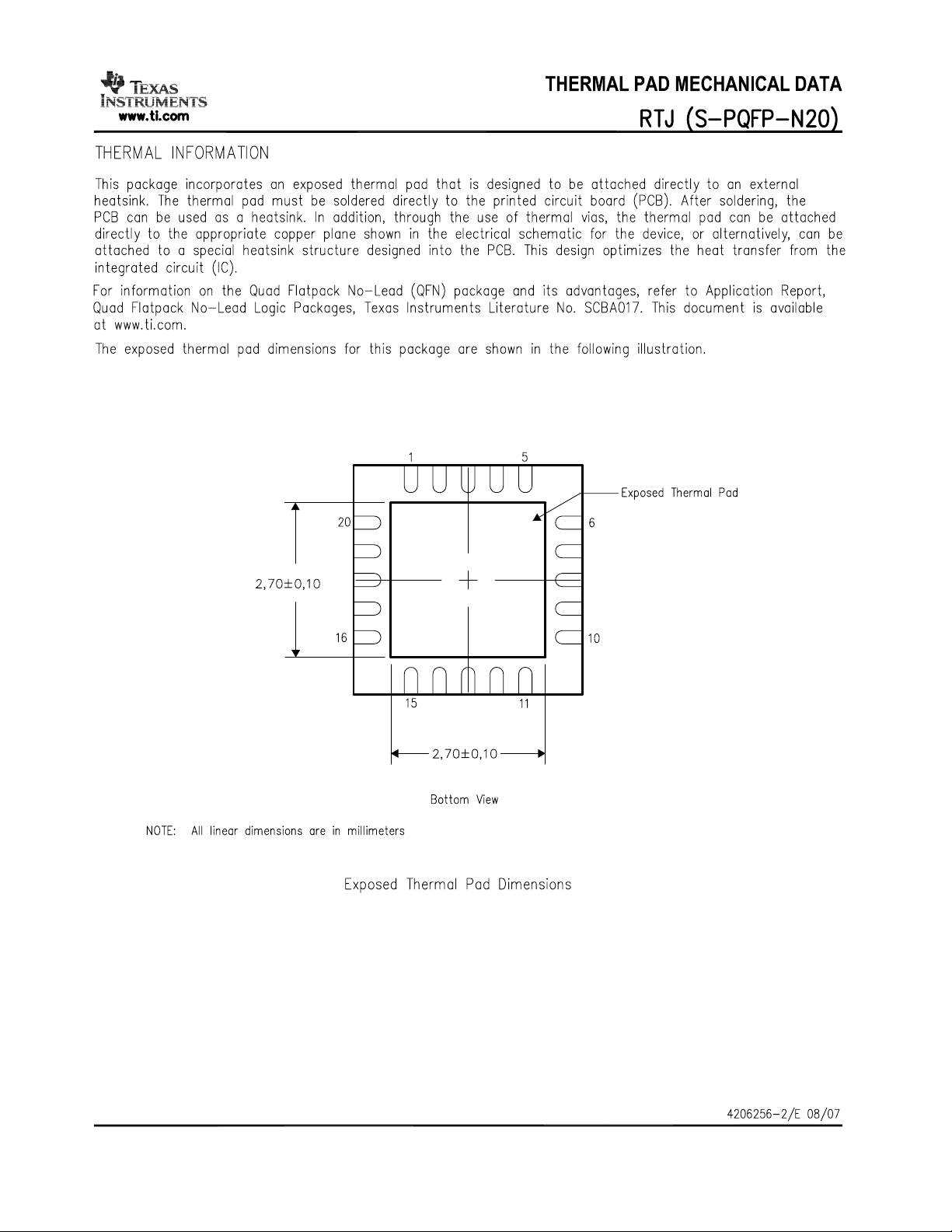
RTJ (QFN) PACKAGE
(TOP VIEW)
YZH (WCSP) PACKAGE
(TOP VIEW)
2 Copyright © 2004 – 2008, Texas Instruments Incorporated
Product Folder Link(s): TPA4411 TPA4411M
www.ti.com
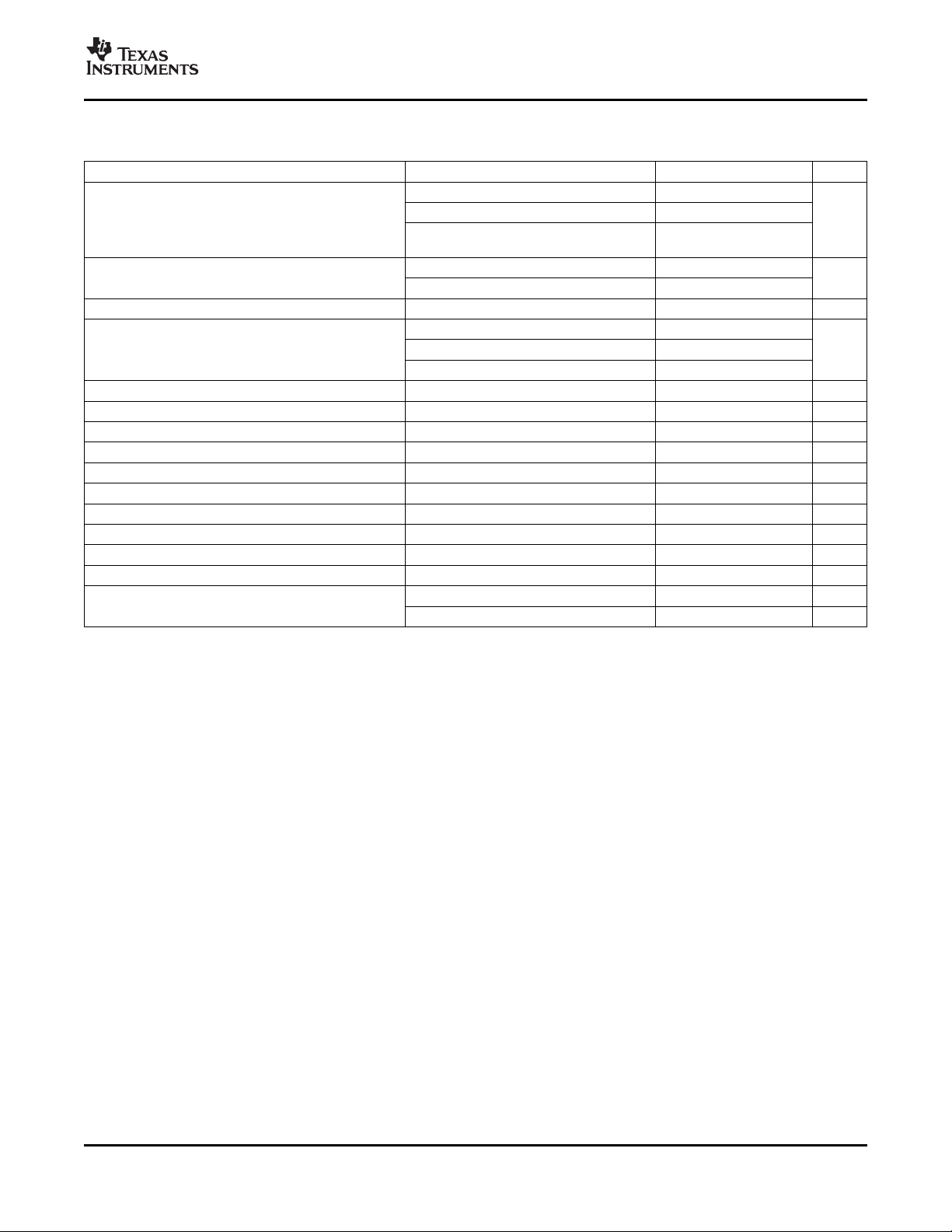
TERMINAL FUNCTIONS
TERMINAL
NAME QFN WCSP
C1P 1 A4 I/O Charge pump flying capacitor positive terminal
PGND 2 B4 I Power ground, connect to ground.
C1N 3 C4 I/O Charge pump flying capacitor negative terminal
4, 6, 8,
NC 12, 16, B3, C3 No connection
20
PVSS 5 D4 O Output from charge pump.
SVSS 7 D3 I Amplifier negative supply, connect to PVSS via star connection.
OUTL 9 D2 O Left audio channel output signal
SVDD 10 D1 I Amplifier positive supply, connect to PVDD via star connection.
OUTR 11 C2 O Right audio channel output signal
INL 13 C1 I Left audio channel input signal
SDR 14 B1 I Right channel shutdown, active low logic.
INR 15 A1 I Right audio channel input signal
SGND 17 A2 I Signal ground, connect to ground.
SDL 18 B2 I Left channel shutdown, active low logic.
PVDD 19 A3 I Supply voltage, connect to positive supply.
Exposed Pad -
I/O DESCRIPTION
Exposed pad must be soldered to a floating plane. Do NOT connect to power or ground.
TPA4411
TPA4411M
SLOS430E – AUGUST 2004 – REVISED MARCH 2008
ABSOLUTE MAXIMUM RATINGS
(1)
over operating free-air temperature range, TA= 25 ° C (unless otherwise noted)
VALUE / UNIT
Supply voltage, AVDD, PVDD – 0.3 V to 5.5 V
V
T
T
T
(1) Stresses beyond those listed under absolute maximum ratings may cause permanent damage to the device. These are stress ratings
Input voltage – 0.3 V to V
I
Output Continuous total power dissipation See Dissipation Rating Table
Operating free-air temperature range – 40 ° C to 85 ° C
A
Operating junction temperature range – 40 ° C to 150 ° C
J
Storage temperature range – 65 ° C to 150 ° C
stg
Lead temperature 1,6 mm (1/16 inch) from case for 10 seconds 260 ° C
only, and functional operation of the device at these or any other conditions beyond those indicated under recommended operating
conditions is not implied. Exposure to absolute-maximum-rated conditions for extended periods may affect device reliability.
DD
+ 0.3 V
Copyright © 2004 – 2008, Texas Instruments Incorporated 3
Product Folder Link(s): TPA4411 TPA4411M
www.ti.com
TPA4411
TPA4411M
SLOS430E – AUGUST 2004 – REVISED MARCH 2008
DISSIPATION RATINGS TABLE
PACKAGE DERATING FACTOR
RTJ
(TPA4411)
RTJ
(TPA4411M)
TA≤ 25 ° C TA= 70 ° C TA= 85 ° C
POWER RATING POWER RATING POWER RATING
5200 mW 41.6 mW/ ° C 3120 mW 2700 mW
3450 mW 34.5 mW/ ° C 1898 mW 1380 mW
YZH 1200 mW 9.21 mW/ ° C 690 mW 600 mW
(1) Derating factor measured with High K board.
AVAILABLE OPTIONS
T
A
PACKAGED DEVICES
20-pin, 4 mm × 4 mm QFN TPA4411RTJ
– 40 ° C to 85 ° C 20-pin, 4 mm × 4 mm QFN TPA4411MRTJ
16-ball, 2.18 mm × 2.18 mm WSCP TPA4411YZH AKT
(1) For the most current package and ordering information, see the Package Option Addendum at the end of this document, or see the TI
website at www.ti.com .
(2) The RTJ package is only available taped and reeled. To order, add the suffix “ R ” to the end of the part number for a reel of 3000, or add
the suffix “ T ” to the end of the part number for a reel of 250 (e.g., TPA4411RTJR).
(1)
(1)
PART NUMBER SYMBOL
(2)
(2)
AKQ
BPB
RECOMMENDED OPERATING CONDITIONS
Supply voltage, AVDD, PVDD 1.8 4.5
V
High-level input voltage SDL, SDR 1.5 V
IH
V
Low-level input voltage SDL, SDR 0.5 V
IL
T
Operating free-air temperature – 40 85 ° C
A
(1) Device can shut down for VDD > 4.5 V to prevent damage to the device.
ELECTRICAL CHARACTERISTICS
TA= 25 ° C (unless otherwise noted)
PARAMETER TEST CONDITIONS MIN TYP MAX UNIT
|VOS| Output offset voltage V
PSRR Power Supply Rejection Ratio V
V
V
High-level output voltage V
OH
Low-level output voltage V
OL
|IIH| High-level input current ( SDL, SDR) V
|IIL| Low-level input current ( SDL, SDR) V
I
Supply Current
DD
= 1.8 V to 4.5 V, Inputs grounded 8 mV
DD
= 1.8 V to 4.5 V – 69 – 80 dB
DD
= 3 V, RL= 16 Ω 2.2 V
DD
= 3 V, RL= 16 Ω – 1.1 V
DD
= 4.5 V, VI= V
DD
= 4.5 V, VI= 0 V 1 µA
DD
V
= 1.8 V, No load, SDL= SDR = V
DD
V
= 3 V, No load, SDL = SDR = V
DD
V
= 4.5 V, No load, SDL = SDR = V
DD
Shutdown mode, V
DD
DD
DD
DD
= 1.8 V to 4.5 V 1 µA
DD
MIN MAX UNIT
5.3 6.5
6.5 8.0 mA
8.0 10.0
(1)
1 µA
V
4 Copyright © 2004 – 2008, Texas Instruments Incorporated
Product Folder Link(s): TPA4411 TPA4411M
www.ti.com
TPA4411
TPA4411M
SLOS430E – AUGUST 2004 – REVISED MARCH 2008
OPERATING CHARACTERISTICS
V
= 3 V , TA= 25 ° C, RL= 16 Ω (unless otherwise noted)
DD
PARAMETER TEST CONDITIONS MIN TYP MAX UNIT
THD = 1%, V
P
O
Output power (Outputs In Phase) mW
THD = 1%, V
THD = 1%, V
Ω
THD+N Total harmonic distortion plus noise
PO= 25 mW, f = 1 kHz 0.054%
PO= 25 mW, f = 20 kHz 0.010%
Crosstallk PO= 20 mW, f = 1 kHz – 83 dB
200-mV
pp
k
SVR
A
v
Δ A
v
Supply ripple rejection ratio 200-mV
pp
200-mV
pp
Closed-loop voltage gain – 1.45 – 1.5 – 1.55 V/V
Gain matching 1%
Slew rate 2.2 V/µs
Maximum capacitive load 400 pF
V
n
Noise output voltage 10 µV
Electrostatic discharge, IEC OUTR, OUTL ± 8 kV
f
osc
Charge pump switching frequency 280 320 420 kHz
Start-up time from shutdown 450 µs
Input impedance 12 15 18 k Ω
SNR Signal-to-noise ratio Po= 40 mW (THD+N = 0.1%) 98 dB
Thermal shutdown
Threshold 150 170 ° C
Hysteresis 15 ° C
= 3 V, f = 1 kHz 50
DD
= 4.5 V, f = 1 kHz 100
DD
= 3 V, f = 1 kHz, RL= 32
DD
50
ripple, f = 217 Hz – 82.5
ripple, f = 1 kHz – 70.4 dB
ripple, f = 20 kHz – 45.1
RMS
Copyright © 2004 – 2008, Texas Instruments Incorporated 5
Product Folder Link(s): TPA4411 TPA4411M
www.ti.com
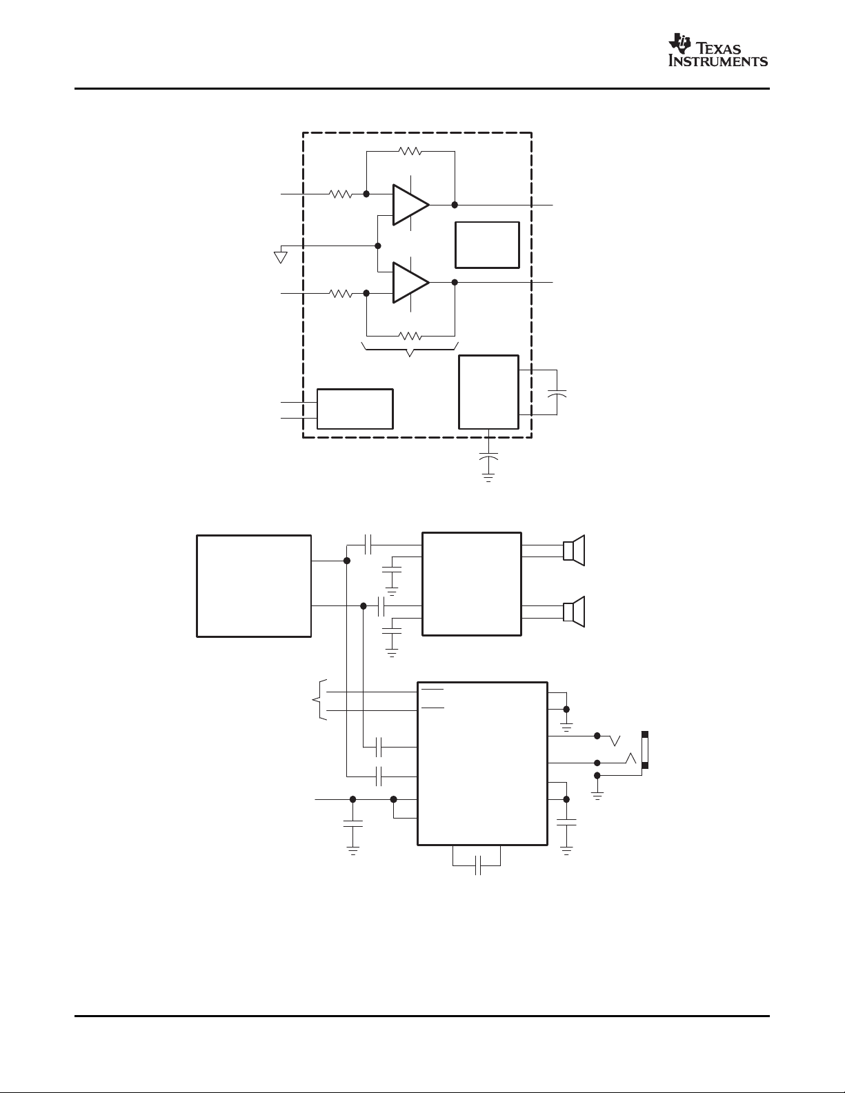
_
+
_
+
SVDD
SVSS
SVDD
SVSS
Charge
Pump
Bias
Circuitry
TPA4411
SGND
Av = −1.5 V/V
Audio Out − R
Audio Out − L
C1P
C1N
PVSS
Audio In − R
Audio In − L
SDx
Short
Circuit
Protection
Shutdown
Control
SV
DD
PV
DD
C1P C1N
SV
SS
PV
SS
OUTR
OUTL
SDR
INL
INR
SDL
1.8 − 4.5 V
TPA4411
TPA2012D2
TLV320AIC26
or
TLV320AIC28
HPL
or
SPK1
HPR
or
SPK2
PGND
SGND
TPA4411
TPA4411M
SLOS430E – AUGUST 2004 – REVISED MARCH 2008
Functional Block Diagram
APPLICATION CIRCUIT
6 Copyright © 2004 – 2008, Texas Instruments Incorporated
Product Folder Link(s): TPA4411 TPA4411M
www.ti.com
0.001
0.01
0.1
1
10
100
1 10
PO − Output Power − mW
THD+N − Total Harmonic Distortion + Noise − %
In Phase
180° Out of Phase
30
VDD = 1.8 V,
RL = 16 Ω,
fIN = 20 Hz
Single
Channel
0.01
0.1
1
10
100
1 10 30
In Phase
Single Channel
180° Out of Phase
PO − Output Power − mW
THD+N − Total Harmonic Distortion + Noise − %
VDD = 1.8 V,
RL = 16 Ω,
fIN = 10 kHz
0.01
0.1
1
10
100
1 10 30
In Phase
Single Channel
180° Out of Phase
PO − Output Power − mW
THD+N − Total Harmonic Distortion + Noise − %
VDD = 1.8 V,
RL = 16 Ω,
fIN = 1 kHz
0.01
0.1
1
10
100
1 10
30
In Phase
Single Channel
180° Out of Phase
PO − Output Power − mW
THD+N − Total Harmonic Distortion + Noise − %
VDD = 1.8 V,
RL = 32 Ω,
fIN = 1 kHz
0.01
0.1
1
10
100
1 10
30
In Phase
180° Out of Phase
Single Channel
PO − Output Power − mW
THD+N − Total Harmonic Distortion + Noise − %
VDD = 1.8 V,
RL = 32 Ω,
fIN = 10 kHz
0.001
0.01
0.1
1
10
100
1 10 30
In Phase
Single Channel
180° Out of Phase
PO − Output Power − mW
THD+N − Total Harmonic Distortion + Noise − %
VDD = 1.8 V,
RL = 32 Ω,
fIN = 20 Hz
SLOS430E – AUGUST 2004 – REVISED MARCH 2008
TYPICAL CHARACTERISTICS
C
= C
(PUMP)
(PVSS)
= 2.2 µF , C
= 1 µF (unless otherwise noted)
IN
Table of Graphs
Total harmonic distortion + noise vs Output power 1 – 24
Total harmonic distortion + noise vs Frequency 25 – 32
Supply voltage rejection ratio vs Frequency 33, 34
Power dissipation vs Output power 35 – 42
Crosstalk vs Frequency 43 – 46
Output power vs Supply voltage 47 – 50
Quiescent supply current vs Supply voltage 51
Output power vs Load resistance 5 – 60
Output spectrum 61
Gain and phase vs Frequency 62, 63
TPA4411
TPA4411M
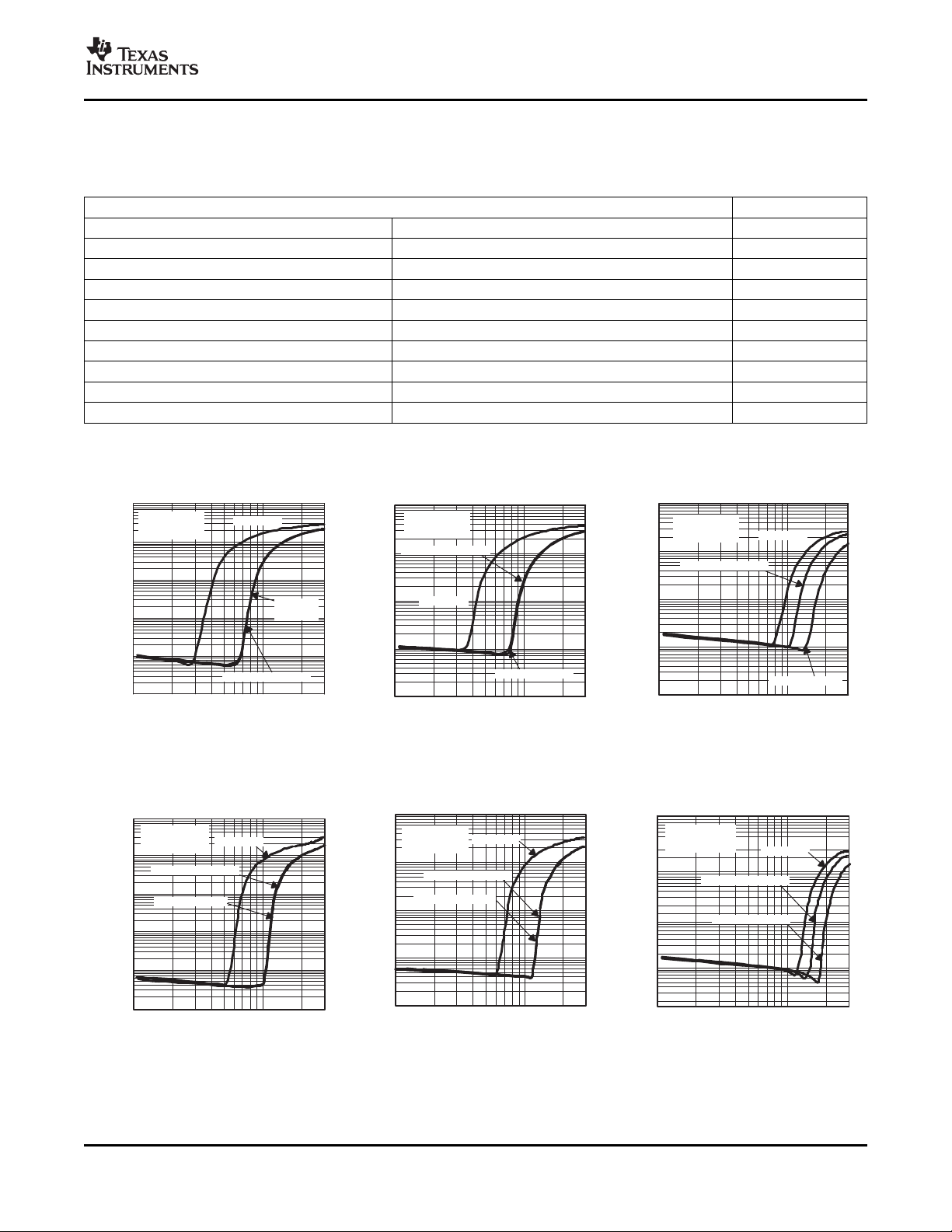
FIGURE
TOTAL HARMONIC DISTORTION TOTAL HARMONIC DISTORTION TOTAL HARMONIC DISTORTION
+ NOISE + NOISE + NOISE
vs vs vs
OUTPUT POWER OUTPUT POWER OUTPUT POWER
Figure 1. Figure 2. Figure 3.
TOTAL HARMONIC DISTORTION TOTAL HARMONIC DISTORTION TOTAL HARMONIC DISTORTION
+ NOISE + NOISE + NOISE
vs vs vs
OUTPUT POWER OUTPUT POWER OUTPUT POWER
Copyright © 2004 – 2008, Texas Instruments Incorporated 7
Figure 4. Figure 5. Figure 6.
Product Folder Link(s): TPA4411 TPA4411M
www.ti.com
0.01
0.1
1
10
100
1 10 100 300
In Phase
Single Channel
180° Out of Phase
PO − Output Power − mW
THD+N − Total Harmonic Distortion + Noise − %
VDD = 3 V,
RL = 16 Ω,
fIN = 10 kHz
0.001
0.01
0.1
1
10
100
1 10 100 300
In Phase
180° Out of Phase
Single Channel
PO − Output Power − mW
THD+N − Total Harmonic Distortion + Noise − %
VDD = 3 V,
RL = 16 Ω,
fIN = 20 Hz
0.01
0.1
1
10
100
1 10 100 300
In Phase
Single Channel
180° Out of Phase
PO − Output Power − mW
THD+N − Total Harmonic Distortion + Noise − %
VDD = 3 V,
RL = 16 Ω,
fIN = 1 kHz
0.001
0.01
0.1
1
10
100
1 10 100 300
PO − Output Power − mW
THD+N − Total Harmonic Distortion + Noise − %
In Phase
Single Channel
180° Out of Phase
VDD = 3 V,
RL = 32 Ω,
fIN = 20 Hz
0.01
0.1
1
10
100
1 10
100 300
In Phase
180° Out of Phase
Single Channel
PO − Output Power − mW
THD+N − Total Harmonic Distortion + Noise − %
VDD = 3 V,
RL = 32 Ω,
fIN = 1 kHz
0.001
0.01
0.1
1
10
100
1 10 100 300
In Phase
180° Out of Phase
Single Channel
PO − Output Power − mW
THD+N − Total Harmonic Distortion + Noise − %
VDD = 3 V,
RL = 32 Ω,
fIN = 10 kHz
0.01
0.1
1
10
100
1 10 100 300
In Phase
180° Out of Phase
Single Channel
PO − Output Power − mW
THD+N − Total Harmonic Distortion + Noise − %
VDD = 3.6 V,
RL = 16 Ω,
fIN = 1 kHz
0.01
0.1
1
10
100
1 10 100 300
In Phase
180° Out of Phase
Single Channel
PO − Output Power − mW
THD+N − Total Harmonic Distortion + Noise − %
VDD = 3.6 V,
RL = 16 Ω,
fIN = 10 kHz
0.001
0.01
0.1
1
10
100
1 10 100
300
In Phase
180° Out of Phase
Single Channel
PO − Output Power − mW
THD+N − Total Harmonic Distortion + Noise − %
VDD = 3.6 V,
RL = 16 Ω,
fIN = 20 Hz
TPA4411
TPA4411M
SLOS430E – AUGUST 2004 – REVISED MARCH 2008
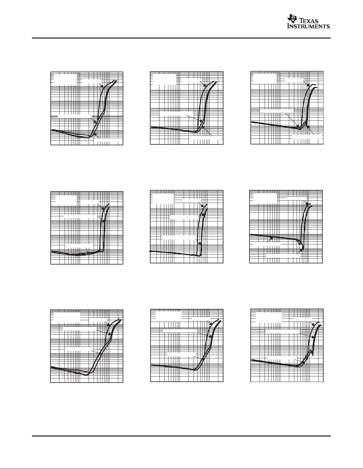
TOTAL HARMONIC DISTORTION TOTAL HARMONIC DISTORTION TOTAL HARMONIC DISTORTION
+ NOISE + NOISE + NOISE
vs vs vs
OUTPUT POWER OUTPUT POWER OUTPUT POWER
Figure 7. Figure 8. Figure 9.
TOTAL HARMONIC DISTORTION TOTAL HARMONIC DISTORTION TOTAL HARMONIC DISTORTION
+ NOISE + NOISE + NOISE
vs vs vs
OUTPUT POWER OUTPUT POWER OUTPUT POWER
TOTAL HARMONIC DISTORTION TOTAL HARMONIC DISTORTION TOTAL HARMONIC DISTORTION
8 Copyright © 2004 – 2008, Texas Instruments Incorporated
Figure 10. Figure 11. Figure 12.
+ NOISE + NOISE + NOISE
vs vs vs
OUTPUT POWER OUTPUT POWER OUTPUT POWER
Figure 13. Figure 14. Figure 15.
Product Folder Link(s): TPA4411 TPA4411M
www.ti.com
0.001
0.01
0.1
1
10
100
1 10 100 300
In Phase
180° Out of Phase
Single Channel
PO − Output Power − mW
THD+N − Total Harmonic Distortion + Noise − %
VDD = 3.6 V,
RL = 32 Ω,
fIN = 20 Hz
0.01
0.1
1
10
100
1 10 100 300
In Phase
180° Out of Phase
Single Channel
PO − Output Power − mW
THD+N − Total Harmonic Distortion + Noise − %
VDD = 3.6 V,
RL = 32 Ω,
fIN = 1 kHz
0.001
0.01
0.1
1
10
100
1 10 100 300
In Phase
180° Out of Phase
P
O
− Output Power − mW
THD+N − Total Harmonic Distortion + Noise − %
Single Channel
VDD = 3.6 V,
RL = 32 Ω,
fIN = 10 kHz
0.001
0.01
0.1
1
10
100
1 10 100 300
In Phase
180° Out of Phase
P
O
− Output Power − mW
THD+N − Total Harmonic Distortion + Noise − %
Single Channel
VDD = 4.5 V,
RL = 16 Ω,
fIN = 20 Hz
0.01
0.1
1
10
100
1 10 100 300
In Phase
180° Out of Phase
P
O
− Output Power − mW
THD+N − Total Harmonic Distortion + Noise − %
Single Channel
VDD = 4.5 V,
RL = 16 Ω,
fIN = 1 k Hz
0.01
0.1
1
10
100
1
100 300
In Phase
180° Out of Phase
Single Channel
P
O
− Output Power − mW
THD+N − Total Harmonic Distortion + Noise − %
10
VDD = 4.5 V,
RL = 16 Ω,
fIN = 10 k Hz
0.001
0.01
0.1
1
10
100
1 10 100 300
In Phase
180° Out of Phase
P
O
− Output Power − mW
THD+N − Total Harmonic Distortion + Noise − %
Single Channel
VDD = 4.5 V,
RL = 32 Ω,
fIN = 20 Hz
0.01
0.1
1
10
100
1 10
100
300
In Phase
180° Out of Phase
P
O
− Output Power − mW
THD+N − Total Harmonic Distortion + Noise − %
Single Channel
VDD = 4.5 V,
RL = 32 Ω,
fIN = 1 kHz
0.01
0.1
1
10
100
1 10 100 300
In Phase
180° Out of Phase
P
O
− Output Power − mW
THD+N − Total Harmonic Distortion + Noise − %
Single Channel
VDD = 4.5 V,
RL = 32 Ω,
fIN = 10 kHz
TPA4411
TPA4411M
SLOS430E – AUGUST 2004 – REVISED MARCH 2008
TOTAL HARMONIC DISTORTION TOTAL HARMONIC DISTORTION TOTAL HARMONIC DISTORTION
+ NOISE + NOISE + NOISE
vs vs vs
OUTPUT POWER OUTPUT POWER OUTPUT POWER
Figure 16. Figure 17. Figure 18.
TOTAL HARMONIC DISTORTION TOTAL HARMONIC DISTORTION TOTAL HARMONIC DISTORTION
+ NOISE + NOISE + NOISE
vs vs vs
OUTPUT POWER OUTPUT POWER OUTPUT POWER
TOTAL HARMONIC DISTORTION TOTAL HARMONIC DISTORTION TOTAL HARMONIC DISTORTION
Copyright © 2004 – 2008, Texas Instruments Incorporated 9
Figure 19. Figure 20. Figure 21.
+ NOISE + NOISE + NOISE
vs vs vs
OUTPUT POWER OUTPUT POWER OUTPUT POWER
Figure 22. Figure 23. Figure 24.
Product Folder Link(s): TPA4411 TPA4411M

www.ti.com
f − Frequency − Hz
THD+N − Total Harmonic Distortion + Noise − %
0.001
0.01
0.1
10
100
1 k 10 k 100 k
1
PO = 2 mW
PO = 5 mW
PO = 6 mW
VDD = 1.8 V
RL = 32 Ω
f − Frequency − Hz
THD+N − Total Harmonic Distortion + Noise − %
0.001
0.01
0.1
10
100
1 k 10 k 100 k
1
PO = 5 mW
PO = 25 mW
VDD = 3 V
RL = 16 Ω
PO = 40 mW
f − Frequency − Hz
THD+N − Total Harmonic Distortion + Noise − %
0.001
0.01
0.1
10
100
1 k 10 k 100 k
1
PO = 1 mW
PO = 2 mW
PO = 3 mW
VDD = 1.8 V
RL = 16 Ω
f − Frequency − Hz
THD+N − Total Harmonic Distortion + Noise − %
0.001
0.01
0.1
10
100
1 k 10 k 100 k
1
PO = 5 mW
VDD = 3 V
RL = 32 Ω
PO = 25 mW
PO = 45 mW
f − Frequency − Hz
THD+N − Total Harmonic Distortion + Noise − %
0.001
0.01
0.1
10
100
1 k 10 k 100 k
1
PO = 5 mW
PO = 20 mW
VDD = 3.6 V
RL = 16 Ω
PO = 40 mW
f − Frequency − Hz
THD+N − Total Harmonic Distortion + Noise − %
0.001
0.01
0.1
10
100 1 k 10 k 100 k
1
PO = 5 mW
VDD = 3.6 V
RL = 32 Ω
PO = 70 mW
PO = 35 mW
−100
−90
−80
−70
−60
−50
−40
−30
−20
−10
0
10 100 1 k 10 k 100 k
k
SVR
− Supply Voltage Rejection Ratio − V
1.8 V
3 V
3.6 V
4.5 V
R
L
= 16 Ω
f − Frequency − Hz
f − Frequency − Hz
THD+N − Total Harmonic Distortion + Noise − %
0.001
0.01
0.1
10
100 1 k 10 k 100 k
1
PO = 5 mW
PO = 50 mW
PO = 35 mW
PO = 25 mW
VDD = 4.5 V
RL = 16 Ω
f − Frequency − Hz
THD+N − Total Harmonic Distortion + Noise − %
0.001
0.01
0.1
10
100
1 k 10 k 100 k
1
PO = 5 mW
PO = 80 mW
PO = 25 mW
PO = 50 mW
VDD = 4.5 V
RL = 32 Ω
TPA4411
TPA4411M
SLOS430E – AUGUST 2004 – REVISED MARCH 2008
TOTAL HARMONIC DISTORTION TOTAL HARMONIC DISTORTION TOTAL HARMONIC DISTORTION
+ NOISE + NOISE + NOISE
vs vs vs
FREQUENCY FREQUENCY FREQUENCY
Figure 25. Figure 26. Figure 27.
TOTAL HARMONIC DISTORTION TOTAL HARMONIC DISTORTION TOTAL HARMONIC DISTORTION
+ NOISE + NOISE + NOISE
vs vs vs
FREQUENCY FREQUENCY FREQUENCY
TOTAL HARMONIC DISTORTION TOTAL HARMONIC DISTORTION SUPPLY VOLTAGE
10 Copyright © 2004 – 2008, Texas Instruments Incorporated
Figure 28. Figure 29. Figure 30.
+ NOISE + NOISE REJECTION RATIO
vs vs vs
FREQUENCY FREQUENCY FREQUENCY
Figure 31. Figure 32. Figure 33.
Product Folder Link(s): TPA4411 TPA4411M

www.ti.com
0
10
20
30
40
50
60
0 5 10 15 20 25 30 35 40
P
O
− Output Power − mW
− Power Dissipation − mW
P
D
In Phase
180° Out of Phase
VDD = 1.8 V,
R
L
= 32 Ω
−100
−90
−80
−70
−60
−50
−40
−30
−20
−10
0
10
100 1 k
10 k 100 k
k
SVR
− Supply Voltage Rejection Ratio − V
1.8 V
3 V
4.5 V
R
L
= 32 Ω
f − Frequency − Hz
3.6 V
0
10
20
30
40
50
60
70
80
0 5 10 15 20 25 30
P
O
− Output Power − mW
− Power Dissipation − mW
P
D
In Phase
180° Out of Phase
VDD = 1.8 V,
R
L
= 16 Ω
0
50
100
150
200
250
300
0 50 100 150 200
P
O
− Output Power − mW
− Power Dissipation − mW
P
D
In Phase
180° Out of Phase
VDD = 3 V,
R
L
= 16 Ω
P
O
− Output Power − mW
− Power Dissipation − mW
P
D
0
50
100
150
200
250
300
350
400
0 50 100 150 200 250 300
In Phase
180° Out of Phase
VDD = 3.6 V,
R
L
= 16 Ω
0
20
40
60
80
100
120
140
160
0
50 100 150 200
P
O
− Output Power − mW
− Power Dissipation − mW
P
D
In Phase
VDD = 3 V,
R
L
= 32 Ω
180° Out of Phase
P
O
− Output Power − mW
− Power Dissipation − mW
P
D
0
50
100
150
200
250
300
350
0 50 100 150 200 250 300
In Phase
180° Out of Phase
VDD = 4.5 V,
R
L
= 32 Ω
0
50
100
150
200
250
0 50 100 150 200 250 300 350
P
O
− Output Power − mW
− Power Dissipation − mW
P
D
In Phase
180° Out of Phase
VDD = 3.6 V,
R
L
= 32 Ω
0
100
200
300
400
500
600
0
50 100 150 200 250
P
O
− Output Power − mW
− Power Dissipation − mW
P
D
In Phase
180° Out of Phase
VDD = 4.5 V,
R
L
= 16 Ω
SLOS430E – AUGUST 2004 – REVISED MARCH 2008
SUPPLY VOLTAGE
REJECTION RATIO POWER DISSIPATION POWER DISSIPATION
vs vs vs
FREQUENCY OUTPUT POWER OUTPUT POWER
Figure 34. Figure 35. Figure 36.
TPA4411
TPA4411M
POWER DISSIPATION POWER DISSIPATION POWER DISSIPATION
vs vs vs
OUTPUT POWER OUTPUT POWER OUTPUT POWER
Figure 37. Figure 38. Figure 39.
POWER DISSIPATION POWER DISSIPATION POWER DISSIPATION
vs vs vs
OUTPUT POWER OUTPUT POWER OUTPUT POWER
Copyright © 2004 – 2008, Texas Instruments Incorporated 11
Figure 40. Figure 41. Figure 42.
Product Folder Link(s): TPA4411 TPA4411M

www.ti.com
−120
−100
−80
−60
−40
−20
0
10 100 1 k 10 k 100 k
Left to Right
Right to Left
f − Frequency − Hz
Crosstalk − dB
VDD = 3 V,
PO = 20 mW
RL = 16 Ω
−120
−100
−80
−60
−40
−20
0
10 100 1 k 10 k
100 k
Left to Right
Right to Left
f − Frequency − Hz
Crosstalk − dB
VDD = 3.6 V,
PO = 1.6 mW
RL = 16 Ω
−120
−100
−80
−60
−40
−20
0
10 100 1 k 10 k 100 k
Left to Right
Right to Left
VDD = 3 V,
PO = 1.6 mW
RL = 16 Ω
f − Frequency − Hz
Crosstalk − dB
−120
−100
−80
−60
−40
−20
0
10 100 1 k 10 k 100 k
Left to Right
Right to Left
f − Frequency − Hz
Crosstalk − dB
VDD = 3.6 V,
PO = 20 mW
RL = 16 Ω
0
20
40
60
80
100
120
1.8 2.3 2.8 3.3 3.8 4.3
180° Out of Phase
In Phase
P
O
− Output Power − mW
VDD − Supply Voltage − V
THD = 1 %
R
L
= 16 Ω
0
50
100
150
200
250
1.8 2.3 2.8 3.3 3.8 4.3
180° Out of Phase
In Phase
P
O
− Output Power − mW
VDD − Supply Voltage − V
THD = 10 %
R
L
= 16 Ω
0
20
40
60
80
100
120
140
160
1.8 2.3 2.8 3.3 3.8 4.3
180° Out of Phase
In Phase
P
O
− Output Power − mW
VDD − Supply Voltage − V
THD = 1 %
R
L
= 32 Ω
0
50
100
150
200
250
1.8 2.3 2.8 3.3 3.8 4.3
180° Out of Phase
In Phase
P
O
− Output Power − mW
VDD − Supply Voltage − V
THD = 10 %
R
L
= 32 Ω
I
DD
− Quiescent Supply Current − mA
VDD − Supply Voltage − V
0
1
2
3
4
5
6
7
8
9
10
0 1 1.5 2 2.5 3 3.5 4 4.5 5
TPA4411
TPA4411M
SLOS430E – AUGUST 2004 – REVISED MARCH 2008
CROSSTALK CROSSTALK CROSSTALK
vs vs vs
FREQUENCY FREQUENCY FREQUENCY
Figure 43. Figure 44. Figure 45.
CROSSTALK OUTPUT POWER OUTPUT POWER
vs vs vs
FREQUENCY SUPPLY VOLTAGE SUPPLY VOLTAGE
SUPPLY VOLTAGE SUPPLY VOLTAGE SUPPLY VOLTAGE
12 Copyright © 2004 – 2008, Texas Instruments Incorporated
Figure 46. Figure 47. Figure 48.
OUTPUT POWER OUTPUT POWER QUIESCENT SUPPLY CURRENT
vs vs vs
Figure 49. Figure 50. Figure 51.
Product Folder Link(s): TPA4411 TPA4411M

www.ti.com
30
40
50
60
70
80
90
100
110
120
0 10 20 30 40 50
2.2 µF
1 µF
0.68 µF
0.47 µF
P
O
− Output Power − mW
RL − Load Resistance − Ω
In Phase,
VDD = 3 V,
THD = 1%,
Vary C
(PUMP)
0
5
10
15
20
25
30
35
40
10 100 1000 10000
Out of Phase
In Phase
P
O
− Output Power − mW
RL − Load Resistance − Ω
VDD = 1.8 V,
THD = 10%,
f
IN
= 1 kHz,
P
O
= P
OUTL
+ P
OUTR
0
5
10
15
20
25
30
10 100 1000 10000
Out of Phase
In Phase
P
O
− Output Power − mW
RL − Load Resistance − Ω
VDD = 1.8 V,
THD = 1%,
f
IN
= 1 kHz,
P
O
= P
OUTL
+ P
OUTR
0
20
40
60
80
100
120
140
160
10 100
1000
10000
Out of Phase
In Phase
P
O
− Output Power − mW
RL − Load Resistance − Ω
VDD = 3 V,
THD = 1%,
f
IN
= 1 kHz,
P
O
= P
OUTL
+ P
OUTR
0
50
100
150
200
250
10
100 1000 10000
Out of Phase
In Phase
P
O
− Output Power − mW
RL − Load Resistance − Ω
VDD = 3 V,
THD = 10%,
f
IN
= 1 kHz,
P
O
= P
OUTL
+ P
OUTR
0
50
100
150
200
250
10 100 1000 10000
Out of Phase
In Phase
P
O
− Output Power − mW
RL − Load Resistance − Ω
VDD = 3.6 V,
THD = 1%,
f
IN
= 1 kHz,
P
O
= P
OUTL
+ P
OUTR
0
50
100
150
200
250
300
350
10 100 1000 10000
Out of Phase
In Phase
P
O
− Output Power − mW
RL − Load Resistance − Ω
VDD = 3.6 V,
THD = 10%,
f
IN
= 1 kHz,
P
O
= P
OUTL
+ P
OUTR
0
50
100
150
200
250
300
350
10 100 1000 10000
Out of Phase
In Phase
P
O
− Output Power − mW
RL − Load Resistance − Ω
VDD = 4.5 V,
THD = 10%,
f
IN
= 1 kHz,
P
O
= P
OUTL
+ P
OUTR
0
50
100
150
200
250
300
350
400
450
500
10 100 1000 10000
Out of Phase
In Phase
P
O
− Output Power − mW
RL − Load Resistance − Ω
VDD = 4.5 V,
THD = 10%,
f
IN
= 1 kHz,
P
O
= P
OUTL
+ P
OUTR
SLOS430E – AUGUST 2004 – REVISED MARCH 2008
OUTPUT POWER OUTPUT POWER OUTPUT POWER
vs vs vs
LOAD RESISTANCE LOAD RESISTANCE LOAD RESISTANCE
Figure 52. Figure 53. Figure 54.
OUTPUT POWER OUTPUT POWER OUTPUT POWER
vs vs vs
LOAD RESISTANCE LOAD RESISTANCE LOAD RESISTANCE
TPA4411
TPA4411M
OUTPUT POWER OUTPUT POWER OUTPUT POWER
LOAD RESISTANCE LOAD RESISTANCE LOAD RESISTANCE
Copyright © 2004 – 2008, Texas Instruments Incorporated 13
Figure 55. Figure 56. Figure 57.
vs vs vs
Figure 58. Figure 59. Figure 60.
Product Folder Link(s): TPA4411 TPA4411M

www.ti.com
-40
-20
0
20
40
60
80
100
0
0.5
1
1.5
2
2.5
3
3.5
Gain
− dB
10 100 1k 10k 100k 1G
f − Frequency − Hz
Phase
− Degrees
VCC=3.6V,
R
L
=16 Ω
Phase
Gain
-40
-20
0
20
40
60
80
100
Phase − Degrees
f − Frequency − Hz
10 100 1k 10k 100k 1G
VCC=3V,
RL=16 Ω
Phase
Gain
Gain − dB
0
0.5
1
1.5
2
2.5
3
3.5
−160
−140
−120
−100
−80
−60
−40
−20
0
20
10 100 1 k 10 k 100 k
Output Spectrum − dBv
f − Frequency − Hz
VO = 1 V
RMS
VDD = 3 V
f
IN
= 1 kHz
R
L
= 32 Ω
TPA4411
TPA4411M
SLOS430E – AUGUST 2004 – REVISED MARCH 2008
GAIN AND PHASE GAIN AND PHASE
vs vs
OUTPUT SPECTRUM FREQUENCY FREQUENCY
Figure 61. Figure 62. Figure 63.
14 Copyright © 2004 – 2008, Texas Instruments Incorporated
Product Folder Link(s): TPA4411 TPA4411M

www.ti.com
f =
c
1
2 R Cp
L O
C =
O
1
2 R fp
L
c
TPA4411
TPA4411M
SLOS430E – AUGUST 2004 – REVISED MARCH 2008
APPLICATION INFORMATION
Headphone Amplifiers
Single-supply headphone amplifiers typically require dc-blocking capacitors. The capacitors are required because
most headphone amplifiers have a dc bias on the outputs pin. If the dc bias is not removed, the output signal is
severely clipped, and large amounts of dc current rush through the headphones, potentially damaging them. The
top drawing in Figure 64 illustrates the conventional headphone amplifier connection to the headphone jack and
output signal.
DC blocking capacitors are often large in value. The headphone speakers (typical resistive values of 16 Ω or 32
Ω ) combine with the dc blocking capacitors to form a high-pass filter. Equation 1 shows the relationship between
the load impedance
C
can be determined using Equation 2 , where the load impedance and the cutoff frequency are known.
O
If fCis low, the capacitor must then have a large value because the load resistance is small. Large capacitance
values require large package sizes. Large package sizes consume PCB area, stand high above the PCB,
increase cost of assembly, and can reduce the fidelity of the audio output signal.
Two different headphone amplifier applications are available that allow for the removal of the output dc blocking
capacitors. The Capless amplifier architecture is implemented in the same manner as the conventional amplifier
with the exception of the headphone jack shield pin. This amplifier provides a reference voltage, which is
connected to the headphone jack shield pin. This is the voltage on which the audio output signals are centered.
This voltage reference is half of the amplifier power supply to allow symmetrical swing of the output voltages. Do
not connect the shield to any GND reference or large currents will result. The scenario can happen if, for
example, an accessory other than a floating GND headphone is plugged into the headphone connector. See the
second block diagram and waveform in Figure 64 .
), the capacitor
L
), and the cutoff frequency (fC).
O
(1)
(2)
Copyright © 2004 – 2008, Texas Instruments Incorporated 15
Product Folder Link(s): TPA4411 TPA4411M

www.ti.com
C
O
C
O
V
OUT
V
OUT
GND
GND
V
DD
V
DD
V /2
DD
V
BIAS
Conventional
Capless
GND
V
DD
V
SS
V
BIAS
DirectPath
TM
fc
IN
+
1
2p RINC
IN
C
IN
+
1
2p fcINR
IN
or
TPA4411
TPA4411M
SLOS430E – AUGUST 2004 – REVISED MARCH 2008
Figure 64. Amplifier Applications
The DirectPath™ amplifier architecture operates from a single supply but makes use of an internal charge pump
to provide a negative voltage rail. Combining the user provided positive rail and the negative rail generated by
the IC, the device operates in what is effectively a split supply mode. The output voltages are now centered at
zero volts with the capability to swing to the positive rail or negative rail. The DirectPath™ amplifier requires no
output dc blocking capacitors, and does not place any voltage on the sleeve. The bottom block diagram and
waveform of Figure 64 illustrate the ground-referenced headphone architecture. This is the architecture of the
TPA4411.
Input-Blocking Capacitors
DC input-blocking capacitors are required to be added in series with the audio signal into the input pins of the
TPA4411 and TPA4411M. These capacitors block the DC portion of the audio source and allow the TPA4411
and TPA4411M inputs to be properly biased to provide maximum performance.
These capacitors form a high-pass filter with the input impedance of the TPA4411 and TPA4411M. The cutoff
frequency is calculated using Equation 3 . For this calculation, the capacitance used is the input-blocking
capacitor and the resistance is the input impedance of the TPA4411 or TPA4411M. Because the gains of both
the TPA4411 and TPA4411M are fixed, the input impedance remains a constant value. Using the input
impedance value from the operating characteristics table, the frequency and/or capacitance can be determined
when one of the two values are given.
(3)
16 Copyright © 2004 – 2008, Texas Instruments Incorporated
Product Folder Link(s): TPA4411 TPA4411M

www.ti.com
0.001
0.01
0.1
1
10 100 1 k 10 k 100 k
f − Frequency − Hz
THD+N − Total Harmonic Distortion + Noise − %
VDD = 3.6 V,
RL = 32 Ω,
PO = 35 mW,
C = 1 µF
C = 2.2 µF
0.1
1
10
100
0.0001 0.001 0.01 0.1 1
THD+N − Total Harmonic Distortion + Noise − %
VDD = 3.6 V,
RL = 16 Ω,
fIN = 20 HZ
C = 1 µF
P
O
− Output Power − mW
In Phase
180° Out of Phase
Single Channel
0.001
0.01
0.1
1
10
100
0.001 0.01 0.1
In Phase
180° Out of Phase
Single Channel
PO − Output Power − mW
THD+N − Total Harmonic Distortion + Noise − %
VDD = 3.6 V,
RL = 16 Ω,
fIN = 20 Hz
C = 2.2 µF
TPA4411
TPA4411M
SLOS430E – AUGUST 2004 – REVISED MARCH 2008
Charge Pump Flying Capacitor and PVSS Capacitor
The charge pump flying capacitor serves to transfer charge during the generation of the negative supply voltage.
The PVSS capacitor must be at least equal to the charge pump capacitor in order to allow maximum charge
transfer. Low ESR capacitors are an ideal selection, and a value of 2.2 µF is typical. Capacitor values that are
smaller than 2.2 µF can be used, but the maximum output power is reduced and the device may not operate to
specifications. Figure 65 through Figure 75 compare the performance of the TPA4411 and TPA4411M with the
recommended 2.2-µF capacitors and 1-µF capacitors.
TOTAL HARMONIC DISTORTION
+ NOISE
vs
FREQUENCY
Copyright © 2004 – 2008, Texas Instruments Incorporated 17
Figure 65.
TOTAL HARMONIC DISTORTION TOTAL HARMONIC DISTORTION
+ NOISE + NOISE
vs vs
OUTPUT POWER OUTPUT POWER
Figure 66. Figure 67.
Product Folder Link(s): TPA4411 TPA4411M

www.ti.com
0.01
0.1
1
10
100
0.001 0.01 0.1
In Phase
180° Out of Phase
Single Channel
PO − Output Power − mW
THD+N − Total Harmonic Distortion + Noise − %
VDD = 3.6 V,
RL = 16 Ω,
fIN = 1 kHz
C = 2.2 µF
0.01
0.1
1
10
100
0.0001 0.001 0.01 0.1
1
THD+N − Total Harmonic Distortion + Noise − %
VDD = 3.6 V,
RL = 16 Ω,
fIN = 1 kHZ
C = 1 µF
P
O
− Output Power − mW
In Phase
180° Out of Phase
Single Channel
0.01
0.1
1
10
100
0.001 0.01 0.1
In Phase
180° Out of Phase
Single Channel
PO − Output Power − mW
THD+N − Total Harmonic Distortion + Noise − %
VDD = 3.6 V,
RL = 16 Ω,
fIN = 10 kHz
C = 2.2 µF
0.001
0.01
0.1
1
10
100
0.0001 0.001 0.01 0.1 1
THD+N − Total Harmonic Distortion + Noise − %
VDD = 3.6 V,
RL = 16 Ω,
fIN = 10 kHZ
C = 1 µF
P
O
− Output Power − mW
In Phase
180° Out of Phase
Single Channel
0.1
1
10
100
0.0001 0.001 0.01 0.1 1
THD+N − Total Harmonic Distortion + Noise − %
VDD = 3.6 V,
RL = 32 Ω,
fIN = 20 HZ
C = 1 µF
P
O
− Output Power − mW
180° Out of Phase
Single Channel
In Phase
0.001
0.01
0.1
1
10
100
0.001 0.01 0.1
In Phase
180° Out of Phase
Single Channel
PO − Output Power − mW
THD+N − Total Harmonic Distortion + Noise − %
VDD = 3.6 V,
RL = 32 Ω,
fIN = 20 Hz
C = 2.2 µF
TPA4411
TPA4411M
SLOS430E – AUGUST 2004 – REVISED MARCH 2008
TOTAL HARMONIC DISTORTION TOTAL HARMONIC DISTORTION
+ NOISE + NOISE
vs vs
OUTPUT POWER OUTPUT POWER
Figure 68. Figure 69.
TOTAL HARMONIC DISTORTION TOTAL HARMONIC DISTORTION
+ NOISE + NOISE
vs vs
OUTPUT POWER OUTPUT POWER
18 Copyright © 2004 – 2008, Texas Instruments Incorporated
Figure 70. Figure 71.
TOTAL HARMONIC DISTORTION TOTAL HARMONIC DISTORTION
+ NOISE + NOISE
vs vs
OUTPUT POWER OUTPUT POWER
Figure 72. Figure 73.
Product Folder Link(s): TPA4411 TPA4411M

www.ti.com
−100
−90
−80
−70
−60
−50
−40
−30
−20
−10
0
10 100 1 k 10 k 100 k
k
SVR
− Supply Voltage Rejection Ratio − V
f − Frequency − Hz
VDD = 3.6 V,
RL = 32 Ω,
C = 1 µF
−100
−90
−80
−70
−60
−50
−40
−30
−20
−10
0
10
100 1 k
10 k 100 k
k
SVR
− Supply Voltage Rejection Ratio − V
1.8 V
3 V
4.5 V
R
L
= 32 Ω
C = 2.2 µF
f − Frequency − Hz
3.6 V
TPA4411
TPA4411M
SLOS430E – AUGUST 2004 – REVISED MARCH 2008
SUPPLY VOLTAGE SUPPLY VOLTAGE
REJECTION RATIO REJECTION RATIO
Decoupling Capacitors
The TPA4411 and TPA4411M are DirectPath™ headphone amplifiers that require adequate power supply
decoupling to ensure that the noise and total harmonic distortion (THD) are low. A good low
equivalent-series-resistance (ESR) ceramic capacitor, typically 2.2 µF, placed as close as possible to the device
V
lead works best. Placing this decoupling capacitor close to the TPA4411 or TPA4411M is important for the
DD
performance of the amplifier. For filtering lower frequency noise signals, a 10-µF or greater capacitor placed near
the audio power amplifier would also help, but it is not required in most applications because of the high PSRR of
this device.
vs vs
FREQUENCY FREQUENCY
Figure 74. Figure 75.
Supply Voltage Limiting At 4.5 V
The TPA4411 and TPA4411M have a built-in charge pump which serves to generate a negative rail for the
headphone amplifier. Because the headphone amplifier operates from a positive voltage and negative voltage
supply, circuitry has been implemented to protect the devices in the amplifier from an overvoltage condition.
Once the supply is above 4.5 V, the TPA4411 and TPA4411M can shut down in an overvoltage protection mode
to prevent damage to the device. The TPA4411 and TPA4411M resume normal operation once the supply is
reduced to 4.5 V or lower.
Layout Recommendations
Exposed Pad On TPA4411RTJ and TPA4411MRTJ Package Option
The exposed metal pad on the TPA4411RTJ and TPA4411MRTJ packages must be soldered down to a pad on
the PCB in order to maintain reliability. The pad on the PCB should be allowed to float and not be connected to
ground or power. Connecting this pad to power or ground prevents the device from working properly because it
is connected internally to PVSS.
TPA4411RTJ and TPA441MRTJ PowerPAD Sizes
Both the TPA4411 and TPA4411M are available in a 4 mm × 4mm QFN. The exposed pad on the bottom of the
package is sized differently between the two devices. The TPA4411RTJ PowerPAD is larger than the
TPA4411MRTJ PowerPAD. Please see the layout and mechanical drawings at the end of the datasheet for
proper sizing.
SGND and PGND Connections
The SGND and PGND pins of the TPA4411 and TPA4411M must be routed separately back to the decoupling
capacitor in order to provide proper device operation. If the SGND and PGND pins are connected directly to each
other, the part functions without risk of failure, but the noise and THD performance do not meet the
specifications.
Copyright © 2004 – 2008, Texas Instruments Incorporated 19
Product Folder Link(s): TPA4411 TPA4411M

www.ti.com
PGND
Control
SV
DD
PV
DD
C1P C1N
2.2 mF
SV
SS
PV
SS
2.2 mF
OUTR
OUTL
1 mF
1 mF
SDR
INL
INR
SDL
2.2 mF
V
CC
TPA4411
SDR SDL
Gain0 Gain1
PV
DD
AV
DD
TPA2012D2
TLV320AIC26
or
TLV320AIC28
CODEC
INL+
INL−
INR+
INR−
HPL
or
SPK1
HPR
or
SPK2
AGND
PGND
SGND
20
19
18
17
16
15
14
13
12
11
10
9
8
7
6
5
4
3
2
1
C4
C2
2.2 mF
C1
2.2 mF
C3
2.2 mF
1.8 − 4.5 V
C5
Shutdown Control
Right Audio Input
Shutdown Control
Left Audio Input
+− + −
1 mF
1 mF
Note: PowerPAD must be soldered down and plane must be floating.
No Output DC-Blocking
Capacitors
TPA4411
TPA4411M
SLOS430E – AUGUST 2004 – REVISED MARCH 2008
20 Copyright © 2004 – 2008, Texas Instruments Incorporated
Product Folder Link(s): TPA4411 TPA4411M
Figure 76. Application Circuit
Figure 77. Typical Circuit

www.ti.com
TPA4411
TPA4411M
SLOS430E – AUGUST 2004 – REVISED MARCH 2008
Copyright © 2004 – 2008, Texas Instruments Incorporated 21
Product Folder Link(s): TPA4411 TPA4411M

PACKAGE OPTION ADDENDUM
www.ti.com
15-Feb-2008
PACKAGING INFORMATION
Orderable Device Status
(1)
Package
Type
Package
Drawing
Pins Package
Qty
Eco Plan
TPA4411MRTJR ACTIVE QFN RTJ 20 3000 Green (RoHS &
no Sb/Br)
TPA4411MRTJRG4 ACTIVE QFN RTJ 20 3000 Green (RoHS &
no Sb/Br)
TPA4411MRTJT ACTIVE QFN RTJ 20 250 Green (RoHS &
no Sb/Br)
TPA4411MRTJTG4 ACTIVE QFN RTJ 20 250 Green (RoHS &
no Sb/Br)
TPA4411RTJR ACTIVE QFN RTJ 20 3000 Green (RoHS &
no Sb/Br)
TPA4411RTJRG4 ACTIVE QFN RTJ 20 3000 Green (RoHS &
no Sb/Br)
TPA4411RTJT ACTIVE QFN RTJ 20 250 Green (RoHS &
no Sb/Br)
TPA4411RTJTG4 ACTIVE QFN RTJ 20 250 Green (RoHS &
no Sb/Br)
TPA4411YZHR ACTIVE DSBGA YZH 16 3000 Green (RoHS &
no Sb/Br)
TPA4411YZHT ACTIVE DSBGA YZH 16 250 Green (RoHS &
no Sb/Br)
(1)
The marketing status values are defined as follows:
ACTIVE: Product device recommended for new designs.
LIFEBUY: TI has announced that the device will be discontinued, and a lifetime-buy period is in effect.
NRND: Not recommended for new designs. Device is in production to support existing customers, but TI does not recommend using this part in
a new design.
PREVIEW: Device has been announced but is not in production. Samples may or may not be available.
OBSOLETE: TI has discontinued the production of the device.
(2)
Lead/Ball Finish MSL Peak Temp
CU NIPDAU Level-2-260C-1 YEAR
CU NIPDAU Level-2-260C-1 YEAR
CU NIPDAU Level-2-260C-1 YEAR
CU NIPDAU Level-2-260C-1 YEAR
CU NIPDAU Level-2-260C-1 YEAR
CU NIPDAU Level-2-260C-1 YEAR
CU NIPDAU Level-2-260C-1 YEAR
CU NIPDAU Level-2-260C-1 YEAR
Call TI Level-1-260C-UNLIM
Call TI Level-1-260C-UNLIM
(3)
(2)
Eco Plan - The planned eco-friendly classification: Pb-Free (RoHS), Pb-Free (RoHS Exempt), or Green (RoHS & no Sb/Br) - please check
http://www.ti.com/productcontent for the latest availability information and additional product content details.
TBD: The Pb-Free/Green conversion plan has not been defined.
Pb-Free (RoHS): TI's terms "Lead-Free" or "Pb-Free" mean semiconductor products that are compatible with the current RoHS requirements
for all 6 substances, including the requirement that lead not exceed 0.1% by weight in homogeneous materials. Where designed to be soldered
at high temperatures, TI Pb-Free products are suitable for use in specified lead-free processes.
Pb-Free (RoHS Exempt): This component has a RoHS exemption for either 1) lead-based flip-chip solder bumps used between the die and
package, or 2) lead-based die adhesive used between the die and leadframe. The component is otherwise considered Pb-Free (RoHS
compatible) as defined above.
Green (RoHS & no Sb/Br): TI defines "Green" to mean Pb-Free (RoHS compatible), and free of Bromine (Br) and Antimony (Sb) based flame
retardants (Br or Sb do not exceed 0.1% by weight in homogeneous material)
(3)
MSL, Peak Temp. -- The Moisture Sensitivity Level rating according to the JEDEC industry standard classifications, and peak solder
temperature.
Important Information and Disclaimer:The information provided on this page represents TI's knowledge and belief as of the date that it is
provided. TI bases its knowledge and belief on information provided by third parties, and makes no representation or warranty as to the
accuracy of such information. Efforts are underway to better integrate information from third parties. TI has taken and continues to take
reasonable steps to provide representative and accurate information but may not have conducted destructive testing or chemical analysis on
incoming materials and chemicals. TI and TI suppliers consider certain information to be proprietary, and thus CAS numbers and other limited
information may not be available for release.
In no event shall TI's liability arising out of such information exceed the total purchase price of the TI part(s) at issue in this document sold by TI
to Customer on an annual basis.
Addendum-Page 1

PACKAGE MATERIALS INFORMATION
www.ti.com
TAPE AND REEL INFORMATION
11-Mar-2008
*All dimensions are nominal
Device Package
TPA4411MRTJR QFN RTJ 20 3000 330.0 12.4 4.3 4.3 1.5 8.0 12.0 Q1
TPA4411MRTJT QFN RTJ 20 250 180.0 12.4 4.3 4.3 1.5 8.0 12.0 Q1
TPA4411RTJR QFN RTJ 20 3000 330.0 12.4 4.3 4.3 1.5 8.0 12.0 Q2
TPA4411RTJT QFN RTJ 20 250 180.0 12.4 4.3 4.3 1.5 8.0 12.0 Q2
TPA4411YZHR DSBGA YZH 16 3000 180.0 8.4 2.35 2.35 0.81 4.0 8.0 Q1
TPA4411YZHR DSBGA YZH 16 3000 178.0 8.4 2.35 2.35 0.81 4.0 8.0 Q1
TPA4411YZHT DSBGA YZH 16 250 180.0 8.4 2.35 2.35 0.81 4.0 8.0 Q1
TPA4411YZHT DSBGA YZH 16 250 178.0 8.4 2.35 2.35 0.81 4.0 8.0 Q1
Type
Package
Drawing
Pins SPQ Reel
Diameter
(mm)
Reel
Width
W1 (mm)
A0 (mm) B0 (mm) K0 (mm) P1
(mm)W(mm)
Pin1
Quadrant
Pack Materials-Page 1

PACKAGE MATERIALS INFORMATION
www.ti.com
11-Mar-2008
*All dimensions are nominal
Device Package Type Package Drawing Pins SPQ Length (mm) Width (mm) Height (mm)
TPA4411MRTJR QFN RTJ 20 3000 346.0 346.0 29.0
TPA4411MRTJT QFN RTJ 20 250 190.5 212.7 31.8
TPA4411RTJR QFN RTJ 20 3000 346.0 346.0 29.0
TPA4411RTJT QFN RTJ 20 250 190.5 212.7 31.8
TPA4411YZHR DSBGA YZH 16 3000 220.0 220.0 34.0
TPA4411YZHR DSBGA YZH 16 3000 217.0 193.0 35.0
TPA4411YZHT DSBGA YZH 16 250 220.0 220.0 34.0
TPA4411YZHT DSBGA YZH 16 250 217.0 193.0 35.0
Pack Materials-Page 2


IMPORTANT NOTICE
Texas Instruments Incorporated and its subsidiaries (TI) reserve the right to make corrections, modifications, enhancements, improvements,
and other changes to its products and services at any time and to discontinue any product or service without notice. Customers should
obtain the latest relevant information before placing orders and should verify that such information is current and complete. All products are
sold subject to TI’s terms and conditions of sale supplied at the time of order acknowledgment.
TI warrants performance of its hardware products to the specifications applicable at the time of sale in accordance with TI’s standard
warranty. Testing and other quality control techniques are used to the extent TI deems necessary to support this warranty. Except where
mandated by government requirements, testing of all parameters of each product is not necessarily performed.
TI assumes no liability for applications assistance or customer product design. Customers are responsible for their products and
applications using TI components. To minimize the risks associated with customer products and applications, customers should provide
adequate design and operating safeguards.
TI does not warrant or represent that any license, either express or implied, is granted under any TI patent right, copyright, mask work right,
or other TI intellectual property right relating to any combination, machine, or process in which TI products or services are used. Information
published by TI regarding third-party products or services does not constitute a license from TI to use such products or services or a
warranty or endorsement thereof. Use of such information may require a license from a third party under the patents or other intellectual
property of the third party, or a license from TI under the patents or other intellectual property of TI.
Reproduction of TI information in TI data books or data sheets is permissible only if reproduction is without alteration and is accompanied
by all associated warranties, conditions, limitations, and notices. Reproduction of this information with alteration is an unfair and deceptive
business practice. TI is not responsible or liable for such altered documentation. Information of third parties may be subject to additional
restrictions.
Resale of TI products or services with statements different from or beyond the parameters stated by TI for that product or service voids all
express and any implied warranties for the associated TI product or service and is an unfair and deceptive business practice. TI is not
responsible or liable for any such statements.
TI products are not authorized for use in safety-critical applications (such as life support) where a failure of the TI product would reasonably
be expected to cause severe personal injury or death, unless officers of the parties have executed an agreement specifically governing
such use. Buyers represent that they have all necessary expertise in the safety and regulatory ramifications of their applications, and
acknowledge and agree that they are solely responsible for all legal, regulatory and safety-related requirements concerning their products
and any use of TI products in such safety-critical applications, notwithstanding any applications-related information or support that may be
provided by TI. Further, Buyers must fully indemnify TI and its representatives against any damages arising out of the use of TI products in
such safety-critical applications.
TI products are neither designed nor intended for use in military/aerospace applications or environments unless the TI products are
specifically designated by TI as military-grade or "enhanced plastic." Only products designated by TI as military-grade meet military
specifications. Buyers acknowledge and agree that any such use of TI products which TI has not designated as military-grade is solely at
the Buyer's risk, and that they are solely responsible for compliance with all legal and regulatory requirements in connection with such use.
TI products are neither designed nor intended for use in automotive applications or environments unless the specific TI products are
designated by TI as compliant with ISO/TS 16949 requirements. Buyers acknowledge and agree that, if they use any non-designated
products in automotive applications, TI will not be responsible for any failure to meet such requirements.
Following are URLs where you can obtain information on other Texas Instruments products and application solutions:
Products Applications
Amplifiers amplifier.ti.com Audio www.ti.com/audio
Data Converters dataconverter.ti.com Automotive www.ti.com/automotive
DSP dsp.ti.com Broadband www.ti.com/broadband
Clocks and Timers www.ti.com/clocks Digital Control www.ti.com/digitalcontrol
Interface interface.ti.com Medical www.ti.com/medical
Logic logic.ti.com Military www.ti.com/military
Power Mgmt power.ti.com Optical Networking www.ti.com/opticalnetwork
Microcontrollers microcontroller.ti.com Security www.ti.com/security
RFID www.ti-rfid.com Telephony www.ti.com/telephony
RF/IF and ZigBee® Solutions www.ti.com/lprf Video & Imaging www.ti.com/video
Mailing Address: Texas Instruments, Post Office Box 655303, Dallas, Texas 75265
Copyright © 2008, Texas Instruments Incorporated
Wireless www.ti.com/wireless
 Loading...