

Page 1

User's Guide
SLOU441–July 2016
TPA3255EVM
This User’s Guide describes the operation of the evaluation module (TPA3255EVM, rev A) for the
TPA3255 315-W Stereo/600-W mono PurePath™ Ultra-HD Analog Input Power Stage. The user’s guide
also provides design information, which includes schematics, BOM, and PCB layout. For questions and
support go to the E2E forums (e2e.ti.com).
The main contents of this document are:
• Hardware descriptions and implementation
• Design information
Related documents:
• TPA3255 Data Sheet (SLASEA8)
Topic ........................................................................................................................... Page
2 Hardware Overview .............................................................................................. 3
3 TPA3255EVM Setup.............................................................................................. 6
4 Using TPA3255EVM in Different Output Configurations............................................ 9
5 Board Layouts, Bill of Materials, and Schematic .................................................... 12
SLOU441–July 2016
Submit Documentation Feedback
Copyright © 2016, Texas Instruments Incorporated
TPA3255EVM
1
Page 2

1 Trademarks
PurePath is a trademark of Texas Instruments.
www.ti.com
2
TPA3255EVM
Copyright © 2016, Texas Instruments Incorporated
Submit Documentation Feedback
SLOU441–July 2016
Page 3
www.ti.com
2 Hardware Overview
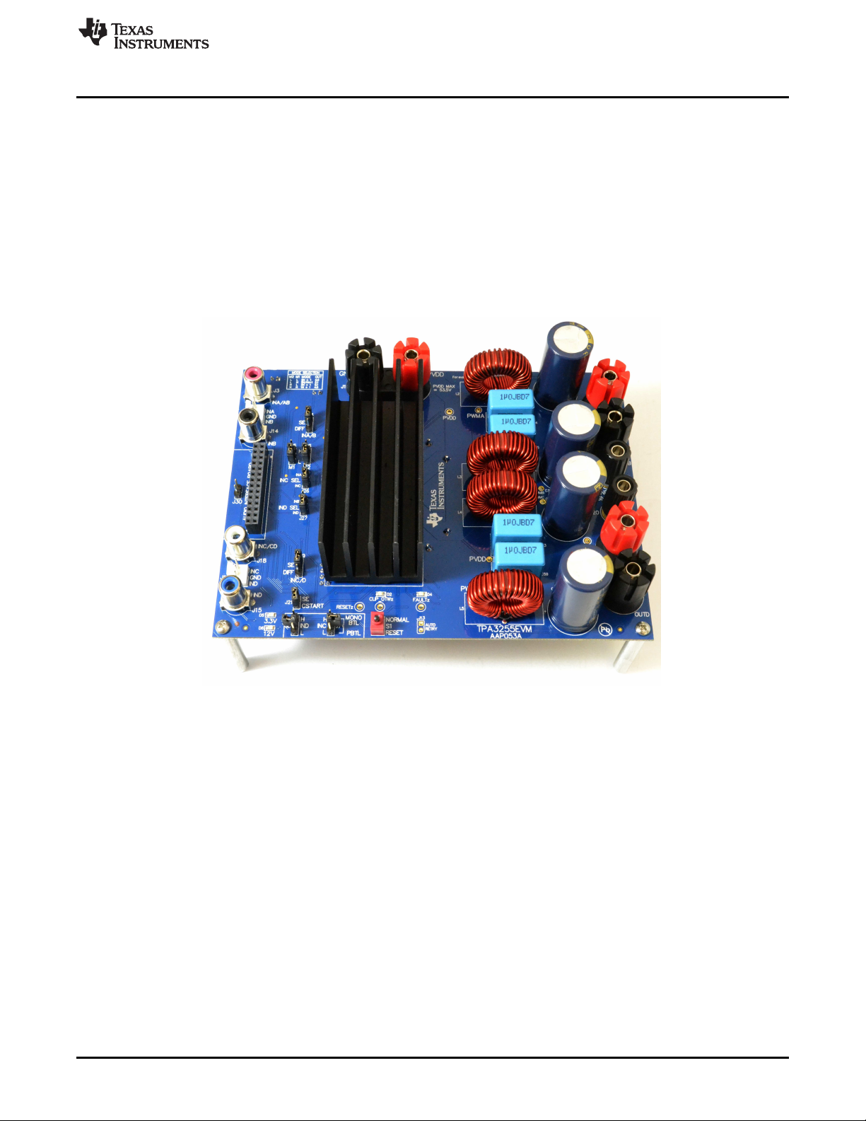
The TPA3255EVM PurePath™ Ultra-HD evaluation module demonstrates the TPA3255DDV integrated
circuit from Texas Instruments. The TPA3255DDV is a high-performance high-power class-D amplifier that
enables true premium sound quality with high-efficiency class-D technology. It features an advance
integrated feedback design and high-speed gate driver error correction (PurePath Ultra-HD), which
enables ultra-low distortion across the audio band and superior audio quality. This EVM supports two BTL
(stereo 2.0) output channels, one PBTL (mono 0.1) output channel, one BTL plus two SE (2.1) output
channels, and four SE (4.0) output channels configurations. The NE5532 is a High Performance Audio Op
Amp designed to allow TPA3255DDV operation with differential or single ended input signals to the EVM
with differential inputs yielding the optimal performance. TPA3255EVM is a complete 2-Vrms analog input
2 × 315-W stereo/1 × 600-W mono high-power amplifier ready for evaluation and excellent listening
experience.
Hardware Overview
2.1 TPA3255EVM Features
The TPA3255EVM has the following features:
• Stereo PurePath Ultra-HD evaluation module
• Self-contained protection system (short circuit, clip, and thermal)
• Standard 4-V
• BTL, PBTL, and SE output configuration support
• Frequency adjust and oscillator sync interface
• Single supply voltage range 14–53.5 V
• Double-sided, plated-through, 2-oz. Cu 2-layer PCB layout
SLOU441–July 2016
Submit Documentation Feedback
differential input or single-ended line input
RMS
Figure 1. TPA3255EVM
Copyright © 2016, Texas Instruments Incorporated
TPA3255EVM
3
Page 4
Hardware Overview
2.2 TPA3255EVM Frequency Adjust
The TPA3255EVM offers hardware trimmed oscillator frequency by external control of the FREQ_ADJ pin.
The Frequency adjust can be used to reduce interference problems while using a radio receiver tuned
within the AM band, the switching frequency can be changed from nominal to lower values. These values
should be chosen such that the nominal and the lower value switching frequencies together results in the
fewest cases of interference throughout the AM band. The oscillator frequency can be selected by the
value of the FREQ_ADJ resistor connected to GND in master mode according to Table 1.
Table 1. Frequency Adjust Master Mode Selection
Master Mode Resistor to GND
Nominal 30 kΩ
AM1 20 kΩ
AM2 10 kΩ
For slave-mode operation, turn off the oscillator by pulling the FREQ_ADJ pin to DVDD. This configures
the OSC_I/O pins as inputs to be slaved from an external differential clock. In a master/slave system interchannel delay is automatically set up between the switching phases of the audio channels, which can be
illustrated by no idle channels switching at the same time. This will not influence the audio output, but only
the switch timing to minimize noise coupling between audio channels through the power supply. This will
optimize audio performance and result in better operating conditions for the power supply. The interchannel delay will be set up for a slave device depending on the polarity of the OSC_I/O connection such
that slave mode 1 is selected by connecting the OSC_I/O of the master device with the OSC_I/O of the
slave device with the same polarity (+ to + and – to –), while slave mode 2 is selected by connecting the
OSC_I/O's with the inverse polarity (+ to – and – to +).
www.ti.com
2.3 TPA3255EVM Single-Ended and Differential Input
The TPA3255EVM supports both differential and single-ended inputs. For single-ended inputs, J4 and/or
J19 jumpers are set to the SE position, so that the TPA3255EVM uses the NE5532 to convert the singleended input signal to differential to properly drive the differential inputs of the TPA3255. The input RCA
jack, J3, is used to provide INA inputs and RCA jack J14 is used to provide INB inputs. RCA jack J18 is
used to provide INC inputs and RCA jack J15 is used to provide IND inputs with differential inputs.
For differential input operation, J4 and/or J19 jumpers are set to the DIFF position, and the TPA3255EVM
uses the NE5532 to buffer the differential input signal to the differential inputs of the TPA3255. The input
RCA jack, J3, is used to provide INA, RCA jack J14 provides INB, RCA jack J18 provides INC, and RCA
jack J15 provides IND with differential inputs.
NOTE: Single-ended input settings on the TPA3255EVM should only be used for channels with
output configuration BTL or PBTL, not SE. For SE output configuration J4 and/or J19
jumpers for that channel must be set to the DIFF position, so the input signal INx is mapped
directly to OUTx.
4
TPA3255EVM
Copyright © 2016, Texas Instruments Incorporated
Submit Documentation Feedback
SLOU441–July 2016
Page 5
www.ti.com
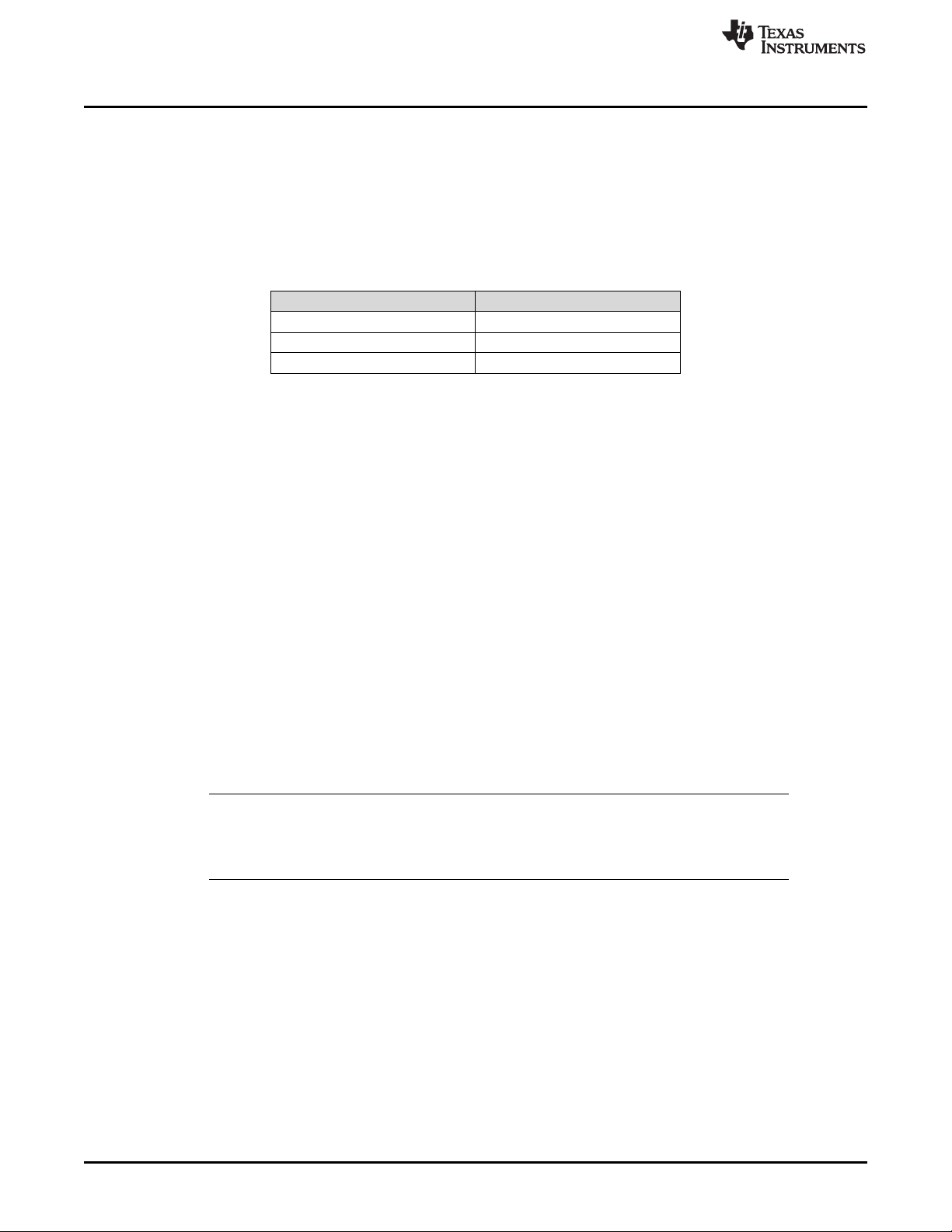
2.4 TPA3255EVM Clip Overtemperature and Fault Indicators
The TPA3255EVM is equipped with LED indicators that illuminate when the FAULT and/or CLIP_OTW pin
goes low. See Table 2 and (SLASEA8) for more details.
Table 2. Fault and Clip Overtemperature Status
FAULT CLIP_OTW Description
0 0
0 0
0 1 Overload (OLP) or undervoltage (UVP). Junction temperature lower than 125°C.
1 0 Junction temperature higher than 125°C (overtemperature warning)
1 1 Junction temperature lower than 125°C and no OLP or UVP faults (normal operation)
Overtemperature (OTE) or overload (OLP) or undervoltage (UVP). Junction temperature higher
than 125°C (overtemperature warning).
Overload (OLP) or undervoltage (UVP). Junction temperature higher than 125°C (overtemperature
warning).
Hardware Overview
SLOU441–July 2016
Submit Documentation Feedback
Copyright © 2016, Texas Instruments Incorporated
TPA3255EVM
5
Page 6
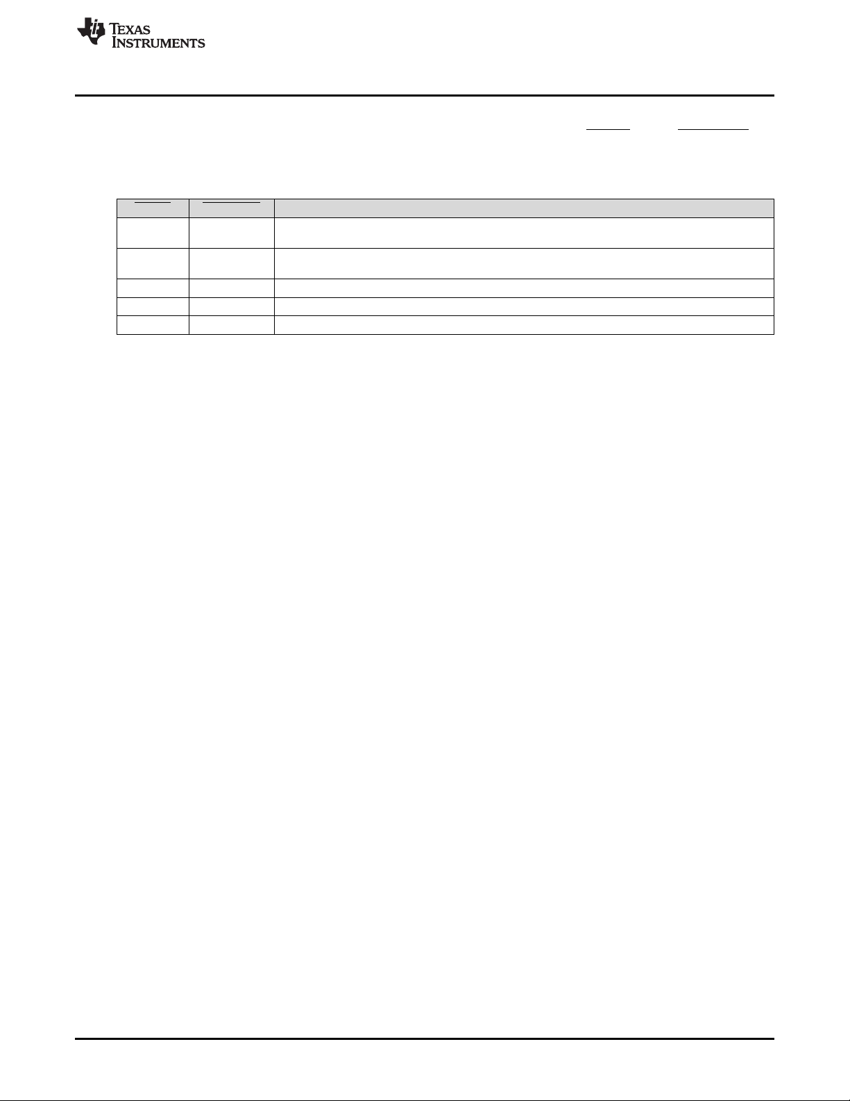
Power Supply
SE A/B Input
DIFF A Input
DIFF B Input
TPA3255
under
Heat Sink
SE C/D Input
DIFF C Input
DIFF D Input
3.3-V and 12-V
LEDs
Warning LEDs
RESET Switch
OUTD
OUTC
GND
GND
OUTB
OUTA
TPA3255EVM Setup
3 TPA3255EVM Setup
This section describes the TPA3255EVM hardware setup and connection.
3.1 TPA3255EVM Setup
Figure 2 illustrates the TPA3255EVM connection.
www.ti.com
3.2 Hardware Requirements
The following hardware is required for this EVM:
• TPA3255EVM (AAP053-001)
• Power supply 5–14 A/18–53.5 V
• Two 2–8 Ω (≈300 W) speakers/resistor loads
• Four speaker/banana cables
• RCA input cables
• Analog output audio source
Figure 2. TPA3255EVM Connections
DC
6
TPA3255EVM
Copyright © 2016, Texas Instruments Incorporated
Submit Documentation Feedback
SLOU441–July 2016
Page 7
www.ti.com
3.3 Hardware Default Setup BTL (2.0)
BTL (2.0) default hardware setup is as follows:
• Remove the EVM from the ESD bag.
• Check that jumpers are in their default state as shown in Figure 1 and Table 3 for stereo BTL
operation:
Table 3. Stereo BTL Default Jumper States
Jumper Setting Comment
J29 IN PVDD to 15-V BUCK
J31 IN 12-V LDO to 12-V TERM
J32 IN 3.3-V LDO to 3.3-V TERM
J33 IN 3.3-V LDO to 3.3-V TERM
J21 IN CSTART SE
J16 3 to 4 MASTER MODE
J5 2 to 3 M1 – BTL
J6 2 to 3 M2 – BTL
J22 IN OUTA CAP SHUNT
J23 IN OUTB CAP SHUNT
J24 IN OUTC CAP SHUNT
J25 IN OUTD CAP SHUNT
J26 2 to 3 INC SELECT
J27 2 to 3 IND SELECT
J7 OUT PBTL SELECT INC
J8 OUT PBTL SELECT IND
J10 OUT INC/D DIFF INPUT
J12 OUT INC/D DIFF INPUT
J4 1 to 2 INA/B SE INPUT
J19 1 to 2 INC/D SE INPUT
TPA3255EVM Setup
• Set S1 to the RESET position.
• Set power supply to 51 V (14–53.5-V range) and current to 10 A (5–14-A range). Do not power up until
all connections are completed.
• Connect power supply to TPA3255 EVM positive terminal to PVDD (RED) and negative terminal to
GND (BLACK).
• Connect left channel speaker/power resistor load (4–8 Ω) to TPA3255 EVM positive output terminal to
OUTA (RED) and AP analog input channel A positive terminal.
• Connect left channel speaker/power resistor load (4–8 Ω) to TPA3255 EVM negative output terminal to
OUTB (BLACK) and AP analog input channel A negative terminal.
• Connect right channel speaker/power resistor load (4–8 Ω) to TPA3255 EVM positive output terminal
to OUTC (RED) and AP analog input channel B positive terminal.
• Connect right channel speaker/power resistor load (4–8 Ω) to TPA3255 EVM negative output terminal
to OUTD (BLACK) and AP analog input channel B negative terminal.
• Be careful not to mix up PVDD, OUTA, and OUTB terminals, since the colors are the same (RED).
• For single-ended stereo inputs, connect AP channel A XLR to RCA male jacks to female RCA jacks
input A/AB (RED) and AP channel B XLR to RCA male jacks to female RCA jacks input C/CD (WHITE)
and set J4 and J19 jumper positions to SE.
• For differential stereo inputs, connect positive RCA male jacks to female RCA jacks input A/AB
(RED) and input C/CD (WHITE) and connect negative RCA male jacks to female RCA jacks input B
(BLUE) and input D (BLACK) and set J4 and J19 jumper positions to DIFF.
• Power up power supply once all the connections are made correctly and the 3.3-V and12-V LEDs
(GREEN) will illuminate.
SLOU441–July 2016
Submit Documentation Feedback
Copyright © 2016, Texas Instruments Incorporated
TPA3255EVM
7
Page 8

TPA3255EVM Setup
• Set S1 to the NORMAL position.
• CLIP_OTWz (ORANGE) and FAULTz (RED) LEDs should be off, if the audio source is off.
NOTE: J3/J10 and J18/J15 can be used for differential inputs to INA/INB and INC/IND, respectively.
Using a smart phone, tablet, or PC with headphone to RCA cable, audio streaming via headphone jack
can begin once the EVM is powered up correctly with jumpers in their default state. Start the media player
of your choice and enjoy the enhanced audio performance TPA3255 provides as a quick check of the
setup.
www.ti.com
8
TPA3255EVM
Copyright © 2016, Texas Instruments Incorporated
Submit Documentation Feedback
SLOU441–July 2016
Page 9

www.ti.com
Using TPA3255EVM in Different Output Configurations
4 Using TPA3255EVM in Different Output Configurations
The TPA3255EVM can be configured for four different output operations. The 2.0 BTL configuration is the
default set up of the TPA3255EVM described in Section 3.3. The remaining three configurations are 2.1
BTL plus two single-ended (SE) outputs, 0.1 PBTL output, and 4.0 single-ended (SE) outputs.
Table 4. Mode Selection Pins
Mode Pins
M2 M1
0 0 2N + 1 2 × BTL Stereo BTL output configuration
0 1 2N/1N + 1 1 × BTL + 2 × SE 2.1 BTL + SE mode
1 0 2N + 1 1 × PBTL
1 1 1N + 1 4 × SE Single-ended output configuration
Input Mode Output Configuration Description
4.1 BTL Plus Two SE (2.1) Operation
Configure the EVM as follows for 2 SE + 1 BTL operation:
Table 5. 2 SE + 1 BTL Default Jumper States
Jumper Setting Comment
J29 IN PVDD to 15-V BUCK
J31 IN 12-V LDO to 12-V TERM
J32 IN 3.3-V LDO to 3.3-V TERM
J33 IN 3.3-V LDO to 3.3-V TERM
J21 IN CSTART SE
J16 3 to 4 MASTER MODE
J5 1 to 2 M1 – 2XSE + BTL
J6 2 to 3 M2 - 2XSE + BTL
J22 IN OUTA CAP SHUNT
J23 IN OUTB CAP SHUNT
J24 OUT OUTC CAP SHUNT
J25 OUT OUTD CAP SHUNT
J26 2 to 3 INC SELECT
J27 2 to 3 IND SELECT
J7 OUT PBTL SELECT INC
J8 OUT PBTL SELECT IND
J10 OUT INC/D DIFF INPUT
J12 OUT INC/D DIFF INPUT
J4 1 to 2 INA/B SE INPUT
J19 1 to 2 INC/D SE INPUT
Paralleled BTL configuration. Connect INPUT_C and INPUT_D to
GND.
• Set J6 to L and J5 to H.
• Connect left (stereo) speaker/power resistor load (2–4 Ω) positive terminal to OUTC and remove
jumper J24.
• Connect right (stereo) speaker/power resistor load (2–4 Ω) positive terminal to OUTD and remove
jumper J25.
• Connect subwoofer (mono) speaker/power resistor load (4–8 Ω) positive terminal to OUTA and
negative terminal to OUTB.
• Set J19 jumper position to DIFF.
• Connect left (stereo) channel input to female RCA jack input C/CD (WHITE) for OUTC speaker.
SLOU441–July 2016
Submit Documentation Feedback
Copyright © 2016, Texas Instruments Incorporated
TPA3255EVM
9
Page 10

Using TPA3255EVM in Different Output Configurations
• Connect right (stereo) channel input to female RCA jack input D (BLACK) for OUTD speaker.
• For single-ended subwoofer (mono) input, connect RCA male jack to female RCA jack input A/AB
(RED) and set J4 jumper positions to SE.
• For differential subwoofer (mono) inputs, connect positive RCA male jack to female RCA jack input
A/AB (RED) and connect negative RCA male jack to female RCA jack input B (YELLOW) and set J4
jumper positions to DIFF.
NOTE: OUTC and OUTD are the single-ended output channels and OUTA and OUTB are the BTL
channel for 2.1 operations.
4.2 PBTL (0.1) Output Operation
Configure the EVM as follows for PBTL operations:
Table 6. PBTL Default Jumper States
Jumper Setting Comment
J29 IN PVDD to 15-V BUCK
J31 IN 12-V LDO to 12-V TERM
J32 IN 3.3-V LDO to 3.3-V TERM
J33 IN 3.3-V LDO to 3.3-V TERM
J21 IN CSTART SE
J16 3 to 4 MASTER MODE
J5 2 to 3 M1 – PBTL
J6 1 to 2 M2 – PBTL
J22 IN OUTA CAP SHUNT
J23 IN OUTB CAP SHUNT
J24 IN OUTC CAP SHUNT
J25 IN OUTD CAP SHUNT
J26 2 to 3 INC SELECT
J27 2 to 3 IND SELECT
J7 2 to 3 PBTL SELECT INC – GND
J8 2 to 3 PBTL SELECT IND – GND
J10 OUT INC/D DIFF INPUT
J12 OUT INC/D DIFF INPUT
J4 1 to 2 INA/B SE INPUT
J19 1 to 2 INC/D SE INPUT
www.ti.com
10
• Set J6 to H and J5 to L.
• Connect speaker/power resistor (2–4 Ω) positive terminal to OUTA and OUTC (OUT A and C shorted).
• Connect speaker/power resistor (2–4 Ω) negative terminal to OUTB and OUTD (OUT B and D
shorted).
• Install PBTL jumpers J7 and J8 (pulls input C and input D to GND).
• For single-ended mono input, connect RCA male jack to female RCA jack input A/AB (RED) and set
J4 jumper positions to SE.
• For differential mono inputs, connect positive RCA male jack to female RCA jack input A/AB (RED)
and connect negative RCA male jack to female RCA jack input B (YELLOW) and set J4 jumper
position to DIFF.
NOTE: INA and INB are the inputs for PBTL and INC and IND are grounded for PBTL operation.
TPA3255EVM
Copyright © 2016, Texas Instruments Incorporated
Submit Documentation Feedback
SLOU441–July 2016
Page 11

www.ti.com
4.3 Single-Ended (SE) Output (4.0) Operation
Configure the EVM as follows for 4 single-ended operations:
Table 7. SE 4.0 Default Jumper States
Jumper Setting Comment
J29 IN PVDD to 15-V BUCK
J31 IN 12-V LDO to 12-V TERM
J32 IN 3.3-V LDO to 3.3-V TERM
J33 IN 3.3-V LDO to 3.3-V TERM
J21 IN CSTART SE
J16 3 to 4 MASTER MODE
J5 1 to 2 M1 – 4XSE
J6 1 to 2 M2 – 4XSE
J22 OUT OUTA CAP SHUNT
J23 OUT OUTB CAP SHUNT
J24 OUT OUTC CAP SHUNT
J25 OUT OUTD CAP SHUNT
J26 2 to 3 INC SELECT
J27 2 to 3 IND SELECT
J7 OUT PBTL SELECT INC
J8 OUT PBTL SELECT IND
J10 OUT INC/D DIFF INPUT
J12 OUT INC/D DIFF INPUT
J4 2 to 3 INA/B DIFF INPUT
J19 2 to 3 INC/D DIFF INPUT
Using TPA3255EVM in Different Output Configurations
• Set J6 to H and J5 to H.
• Connect speaker/power resistor (2–4 Ω) positive terminal to OUTA and remove jumper J22.
• Connect speaker/power resistor (2–4 Ω) positive terminal to OUTB and remove jumper J23.
• Connect speaker/power resistor (2–4 Ω) positive terminal to OUTC and remove jumper J24.
• Connect speaker/power resistor (2–4 Ω) positive terminal to OUTD and remove jumper J25.
• Set both J4 and J19 jumpers position to DIFF.
• Connect input to female RCA jack input A/AB (RED) for OUTA speaker.
• Connect input to female RCA jack input B (YELLOW) for OUTB speaker.
• Connect input to female RCA jack input C/CD (WHITE) for OUTC speaker.
• Connect input to female RCA jack input D (BLACK) for OUTD speaker.
spacer
spacer
spacer
spacer
spacer
NOTE: The performance of the TPA3255EVM/TPA3255DDV is dependent on the power supply.
Design the power supply with margins that can deliver the needed power. In low-frequency
applications additional bulk capacitance may be needed. Replacing the bulk capacitors on
the TPA3255EVM with more capacitance may be necessary, depending on the power supply
used.
SLOU441–July 2016
Submit Documentation Feedback
Copyright © 2016, Texas Instruments Incorporated
TPA3255EVM
11
Page 12

Board Layouts, Bill of Materials, and Schematic
5 Board Layouts, Bill of Materials, and Schematic
5.1 TPA3255EVM Board Layouts
Figure 3 and Figure 4 illustrate the board layouts for the EVM.
www.ti.com
Figure 3. TPA3255EVM Top Composite Assembly
Figure 4. TPA3255EVM Bottom Composite Assembly
12
TPA3255EVM
Copyright © 2016, Texas Instruments Incorporated
Submit Documentation Feedback
SLOU441–July 2016
Page 13

120 mm
160 mm
www.ti.com
5.2 TPA3255EVM Board Dimension
Figure 5 illustrates the TPA3255EVM board dimensions, which are 140 mm × 120 mm.
Figure 5. TPA3255EVM Board Dimension
Board Layouts, Bill of Materials, and Schematic
SLOU441–July 2016
Submit Documentation Feedback
Copyright © 2016, Texas Instruments Incorporated
TPA3255EVM
13
Page 14

Board Layouts, Bill of Materials, and Schematic
5.3 Bill of Materials
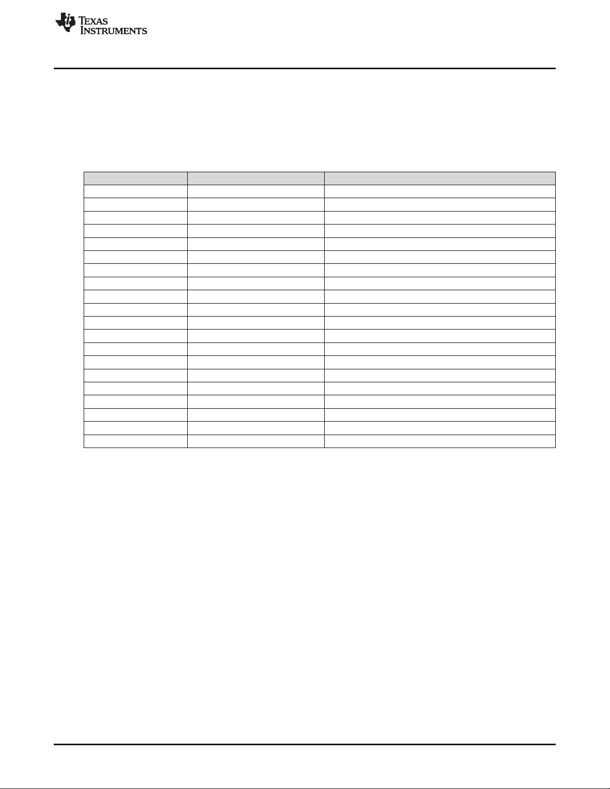
Table 8 displays the BOM for this EVM.
www.ti.com
Table 8. Bill of Materials
Designator
!PCB1 1 Printed Circuit Board AAP053 Any
C1 1 0.047 µf CAP, CERM, 0.047 µF, 25
C2 1 0.1 µf CAP, CERM, 0.1 µF, 100
C3, C32, C33,
C47, C48, C83,
C84
C4 1 2.2 µf CAP, CERM, 2.2 µF, 100
C5 1 47µf CAP, AL, 47 µF, 16 V, ±
C6 1 4.7µf CAP, CERM, 4.7 µF, 25 V,
C7 1 5600 pF CAP, CERM, 5600 pF, 50
C8, C50 2 0.47µf CAP, CERM, 0.47 µF, 25
C9, C13, C14,
C15, C22, C51,
C67, C68, C69,
C72, C82
C10 1 100 µf CAP, AL, 100 µF, 6.3 V, ±
C11, C26, C37,
C45, C61
C12 1 4700 pF CAP, CERM, 4700 pF, 50
C16, C53, C70,
C81
C17, C20, C28,
C38, C55, C62,
C63, C66, C71
C18, C23, C57,
C65
C19, C30, C58,
C64
C21, C34, C42,
C56
C24, C35, C43,
C59
C25, C36, C44,
C60
C27, C29, C52,
C54
C31, C46 2 4700 µf CAP, AL, 4700 µF, 80 V, ±
C39 1 47 µf CAP, AL, 47 µF, 63 V, ±
C40, C41 2 1 µf CAP, CERM, 1 µF, 16 V, ±
Quantit
11 0.1 µf CAP, CERM, 0.1 µF, 50 V,
Value Description
y
V, ± 10%, X7R, 0402
V, ± 10%, X7R, 0603
7 1 µf CAP, CERM, 1 µF, 100 V,
5 0.01 µf CAP, CERM, 0.01 µF, 100
4 10 µf CAP, CERM, 10 µF, 16 V,
9 10 µf CAP, AL, 10 µF, 16 V, ±
4 22 pF CAP, CERM, 22 pF, 50 V,
4 100 pF CAP, CERM, 100 pF, 50 V,
4 1500 µf CAP, AL, 1500 µF, 63 V, ±
4 1 µf CAP, Film, 1 µF, 250 V, ±
4 1000 pF CAP, CERM, 1000 pF, 100
4 0.033 µf CAP, CERM, 0.033 µF, 25
± 10%, X7R, 1206
V, ± 10%, X7R, 1210
20%, 0.36 Ω, SMD
± 10%, X7R, 1206
V, ± 10%, X7R, 0603
V, ± 10%, X7R, 0603
± 10%, X7R, 0603
20%, 0.7 Ω, SMD
V, ± 10%, X7R, 0603
V, ± 10%, X7R, 0603
± 10%, X5R, 0805
20%, 1.35 Ω, SMD
± 5%, C0G/NP0, 0603
± 5%, C0G/NP0, 0603
20%, 0.03 Ω, AEC-Q200
Grade 2, TH
5%, TH
V, ± 5%, C0G/NP0, 1206
V, ± 10%, X7R, 0603
20%, 0.071 Ω, TH
20%, 0.65 Ω, SMD
10%, X7R, 0603
Package
Reference
402 GRM155R71E473KA
603 GRM188R72A104KA
1206 GRM31CR72A105KA
1210 C1210C225K1RACTUKemet
SMT Radial D EEE-FK1C470P Panasonic
1206 GRM31CR71E475KA
603 GRM188R71H562KA
603 GRM188R71E474KA
603 C0603C104K5RACTUKemet
SMT Radial C EEE-FK0J101UR Panasonic
603 06031C103KAT2A AVX
603 C0603X472K5RACTUKemet
805 EMK212BJ106KG-T Taiyo Yuden
SMT Radial B EEE-FK1C100R Panasonic
603 GRM1885C1H220JA
603 GRM1885C1H101JA
Dia 18 mm EEU-FC1J152 Panasonic
18mm × 9.5mm ×
17.5 mm
1206 12061A102JAT2A AVX
603 GRM188R71E333KA
D35 mm × L30mmSLPX472M080H3P3 Cornell Dubilier
SMT Radial F EEE-FK1J470P Panasonic
603 GRM188R71C105KA
Part NUmber Manufacturer
88D
35J
01L
88L
01D
12D
01D
01D
PHE426HB7100JR06 Kemet
01D
12D
MuRata
MuRata
MuRata
MuRata
MuRata
MuRata
MuRata
MuRata
MuRata
Electronics
MuRata
14
TPA3255EVM
Submit Documentation Feedback
SLOU441–July 2016
Copyright © 2016, Texas Instruments Incorporated
Page 15

www.ti.com
Board Layouts, Bill of Materials, and Schematic
Table 8. Bill of Materials (continued)
Designator
C49 1 0.01 µf CAP, CERM, 0.01 µF, 50
D1 1 100 V Diode, Schottky, 100 V, 1
D2 1 Orange LED, Orange, SMD LED_0805 LTST-C170KFKT Lite-On
D3 1 100 V Diode, Schottky, 100 V, 3
D4 1 Red LED, Red, SMD LED_0805 LTST-C170KRKT Lite-On
D5 1 Green LED, Green, SMD LED_0805 LTST-C171GKT Lite-On
H1 1 Heat Sink, Vertical Heatsink ATS-TI1OP-519-C1-R3Advanced
H2, H3, H4, H5,
H6, H12, H13
H7, H8, H9,
H10, H11
J1, J2, J9 3 Dual Binding Posts with
J3 1 RCA Jack, Vertical, Red,THRCA JACK, RED RCJ-022 CUI Inc.
Quantit
Value Description
y
V, ± 10%, X7R, 0603
A, SMA
A, SMA
7 MACHINE SCREW PAN
5 Standoff, Hex, 25-mm
PHILLIPS M3 5mm
Length, M3, Aluminum
Base, 2x1, TH
Package
Reference
603 GRM188R71H103KA
SMA B1100-13-F Diodes Inc.
SMA SK310A-TP Micro Commercial
Screw M3 Phillips
head
Standoff M3 24438 Keystone
Dual Binding
Posts with Base,
2 × 1, TH
Part NUmber Manufacturer
01D
MPMS 003 0005 PH B&F Fastener
6883 Pomona
MuRata
Components
Thermal Solutions
Supply
Electronics
J4, J5, J6, J7,
J8, J19, J26,
J27
J10, J12 2 Header, 2.54 mm, 3 × 1,THHeader, 2.54 mm,
J11, J20 2 Binding Post, BLACK, TH 11.4 mm × 27.2mm7007 Keystone
J14 1 RCA Jack, Vertical, Black,THRCA Jack,
J15 1 RCA Jack, Vertical, Blue,THRCA Jack,
J16 1 Header, 100 mil, 4 × 2, Tin,THHeader, 4 × 2,
J17 1 Header (friction lock), 100
J18 1 RCA Jack, Vertical, White,THRCA JACK,
J21, J30 2 Header, 100 mil, 2 × 1,
J22, J23, J24,
J25, J29
J28 1 Receptacle, 100 mil, 8 × 2,
L1 1 100 µH Inductor, Shielded Drum
L2, L3, L4, L5 4 10 µH Inductor, Toroid, Powdered
L6 1 10 µH Inductor, Wirewound, 10
8 Header, 100 mil, 3 × 1,
Gold, TH
mil, 4 × 1, Gold, TH
Gold, TH
5 JUMPER TIN SMD 6.85 mm × 0.97
Gold, TH
Core, Ferrite, 100 µH, 1.5
A, 0.165 Ω, SMD
Iron, 10 µH, 6.1 A, 0.026
Ω, TH
µH, 0.8 A, 0.204 Ω, SMD
PBC03SAAN PBC03SAAN Sullins Connector
3 × 1, TH
Vertical, Black,
TH
Vertical, Blue, TH
100 mil, Tin
Header 4 × 1
keyed
WHITE
Sullins 100 mil, 1
× 2, 230 mil
above insulator
mm × 2.51 mm
Receptacle, 8 ×
2, Body 21.08
mm × 4.95 mm,
Pitch 2.54 mm
10 mm × 5 mm ×
10 mm
28.6 mm × 12.3mmMA5172-AE Coilcraft
2-Pin SMD, Body
4 mm × 4 mm,
Height 1.2 mm
Solutions
22-11-2032 Molex
RCJ-021 CUI Inc.
RCJ-025 CUI Inc.
PEC04DAAN Sullins Connector
Solutions
22112042 Molex
RCJ-023 CUI Inc.
PBC02SAAN Sullins Connector
Solutions
S1911-46R Harwin
SSQ-108-02-G-D Samtec
7447714101 Wurth Elektronik
NRS4012T100MDGJVTaiyo Yuden
SLOU441–July 2016
Submit Documentation Feedback
Copyright © 2016, Texas Instruments Incorporated
TPA3255EVM
15
Page 16

Board Layouts, Bill of Materials, and Schematic
Table 8. Bill of Materials (continued)
Designator
L7 1 10 µH Inductor, Wirewound, 10
Q1, Q2 2 60 V MOSFET, N-CH, 60 V,
R1, R3, R4,
R12, R30, R44,
R46
R2 1 182 k RES, 182 k, 1%, 0.125 W,
R5, R10, R19,
R23, R33, R35
R6 1 100 k RES, 100 k, 1%, 0.1 W,
R7, R8, R20,
R21, R25, R27,
R37, R38, R41,
R42
R9, R43, R45,
R48
R11, R14, R18,
R22
R13 1 22.0 k RES, 22.0 k, 1%, 0.1 W,
R15, R36, R52 3 10.0 k RES, 10.0 k, 1%, 0.1 W,
R16 1 20.0 k RES, 20.0 k, 1%, 0.1 W,
R17 1 30.0 k RES, 30.0 k, 1%, 0.1 W,
R24, R28 2 47 k RES, 47 k, 5%, 0.1 W,
R26 1 3.30 k RES, 3.30 k, 1%, 0.1 W,
R29, R31 2 1.00 k RES, 1.00 k, 1%, 0.1 W,
R32 1 12.0 k RES, 12.0 k, 1%, 0.1 W,
R34 1 360 RES, 360, 5%, 0.063 W,
R39 1 4.99 k RES, 4.99 k, 1%, 0.063 W,
R40 1 1.00 k RES, 1.00 k, 1%, 0.063 W,
S1 1 Switch, SPDT, On-On, 2
SH1, SH2, SH3,
SH4, SH5, SH6,
SH7, SH8
U1 1 High Voltage 1A Step
U2 1 1A Low Dropout Regulator,
U3 1 FIXED LOW-DROPOUT
Quantit
10 10.0 k RES, 10.0 k, 0.1%, 0.1 W,
Value Description
y
µH, 0.08 A, 0.36 Ω, SMD
0.17 A, SOT-23
7 0 RES, 0, 5%, 0.1 W, 0603 603 CRCW06030000Z0EAVishay-Dale
0805
6 100 RES, 100, 1%, 0.1 W,
4 100 k RES, 100 k, 1%, 0.063 W,
4 3.3 RES, 3.3, 5%, 0.1 W, 0603 603 CRCW06033R30JNEAVishay-Dale
8 1 × 2 Shunt, 100 mil, Gold
0603
0603
0603
0402
0603
0603
0603
0603
0603
0603
0603
0603
0402
0402
0402
Pos, TH
plated, Black
Down Switching Regulator,
10-pin LLP, Pb-Free
4-pin SOT-223, Pb-Free
VOLTAGE REGULATOR,
DCY0003A
www.ti.com
Package
Reference
603 GLFR1608T100M-LR TDK
SOT-23 2N7002-7-F Diodes Inc.
805 ERJ-6ENF1823V Panasonic
603 CRCW0603100RFKEAVishay-Dale
603 CRCW0603100KFKEAVishay-Dale
603 RT0603BRD0710KL Yageo America
402 CRCW0402100KFKEDVishay-Dale
603 RC0603FR-0722KL Yageo America
603 CRCW060310K0FKEAVishay-Dale
603 RC0603FR-0720KL Yageo America
603 RC0603FR-0730KL Yageo America
603 RC0603JR-0747KL Yageo America
603 RC0603FR-073K3L Yageo America
603 CRCW06031K00FKEAVishay-Dale
603 ERJ-3EKF1202V Panasonic
402 CRCW0402360RJNEDVishay-Dale
402 CRCW04024K99FKEDVishay-Dale
402 CRCW04021K00FKEDVishay-Dale
Switch, 7 mm ×
4.5 mm
Shunt 969102-0000-DA 3M
SDC10A LM5010ASD/NOPB Texas
MP04A LM2940IMP-
DCY0003A TLV1117-33IDCY Texas
Part NUmber Manufacturer
200USP1T1A1M2RE E-Switch
Instruments
12/NOPB
Texas
Instruments
Instruments
16
TPA3255EVM
Submit Documentation Feedback
SLOU441–July 2016
Copyright © 2016, Texas Instruments Incorporated
Page 17

www.ti.com
Table 8. Bill of Materials (continued)
Designator
U4 1 150W Stereo/300W MONO
U5, U6 2 Dual Low-Noise
U7 1 ULTRA-SMALL SUPPLY
C73, C74, C75,
C76
C77, C78, C79,
C80
FID1, FID2,
FID3, FID4,
FID5, FID6
J13 0 Header, 100 mil, 2 × 1,
R47, R49, R50,
R51
R53, R54, R55,
R56
TP1, TP2, TP3,
TP4, TP5, TP6,
TP7, TP8, TP9,
TP10, TP11,
TP12, TP13,
TP14
Quantit
Value Description
y
PurePath HD Analog-input
Power Stage, DDV0044D
Operational Amplifier, 10 to
30 V, 0 to 70 degC, 8-pin
SOIC (D0008A), Green
(RoHS& no Sb/Br)
VOLTAGE
SUPERVISORS,
DCK0005A
0 22 pF CAP, CERM, 22 pF, 50 V,
0 1 µf CAP, CERM, 1 µF, 50 V, ±
0 Fiducial mark. There is
0 10.0 k RES, 10.0 k, 1%, 0.1 W,
0 3.3 RES, 3.3, 5%, 0.75 W,
0 Test Point, Multipurpose,
± 5%, C0G/NP0, 0603
10%, X7R, 1206
nothing to buy or mount.
Gold, TH
0603
2010
Grey, TH
Board Layouts, Bill of Materials, and Schematic
Package
Reference
DDV0044D TPA3255D2DDVR Texas
D0008A NE5532ADR Texas
DCK0005A TPS3802K33DCKR Texas
603 GRM1885C1H220JA
1206 GRM31MR71H105KA
N/A N/A N/A
Sullins 100 mil, 1
× 2, 230 mil
above insulator
603 CRCW060310K0FKEAVishay-Dale
2010 CRCW20103R30JNEFVishay-Dale
Grey
Multipurpose
Testpoint
Part NUmber Manufacturer
Instruments
Instruments
Instruments
MuRata
01D
MuRata
88L
PBC02SAAN Sullins Connector
Solutions
5128 Keystone
SLOU441–July 2016
Submit Documentation Feedback
Copyright © 2016, Texas Instruments Incorporated
TPA3255EVM
17
Page 18

GND
10.0k
R38
VMID
GND
1
2
3
4
8
U6A
NE5532ADR
5
6
7
4
8
U6B
NE5532ADR
10.0k
R27
10.0k
R20
10.0k
R21
VMID
0.1uF
C51
GND GND
10µF
C53
GND
10.0k
R25
10µF
C70
22pF
C65
22pF
C57
VMID
1
2
3
J19
SE
DIFF
0.1uF
C72
GND
GND
1
2
3
4
8
U5A
NE5532ADR
5
6
7
4
8
U5B
NE5532ADR
10.0k
R42
10.0k
R7
10.0k
R8
VMID
+12V-OA
0.1uF
C15
GND GND
10µF
C16
GND
10.0k
R41
22pF
C23
22pF
C18
VMID
1
2
3
J4
SE
DIFF
GND
GND
100k
R48
22pF
C73DNP
DNP
10.0k
R47DNP
DNP
0
R4
0
R12
0
R44
0
R46
22pF
C74DNP
DNP
+12V
GND
10µF
C20
10µF
C71
10µF
C62
10µF
C66
1
2
3
J10
INPUT SE A
SE AB
DIFF A+
INPUT SE B
DIFF A-
INPUT SE D
DIFF C-
10.0k
R49DNP
DNP
GND
10µF
C81
10uH 0.8A
L6
GND
10.0k
R36
10.0k
R52
INA
INB
OUTA
OUTB
+12V-OA
+12V-OA
INC
IND
10.0k
R50DNP
DNP
22pF
C75DNP
DNP
22pF
C76DNP
DNP
10.0k
R51DNP
DNP
OUTC
OUTD
RCA INPUT
LEFT+
RCA INPUT
LEFT-
RCA INPUT
RIGHT-
INB-RCA
IND-RCA
GND
1
2
3
J12
1
2
3
J14
INB
1
2
3
J15
IND
1
2
3
J3
INA/AB
INA-RCA
100k
R43
100k
R9
GND
100k
R45
INPUT SE C
SE CD
DIFF C+
RCA INPUT
RIGHT+
INC-RCA
1
2
3
J18
INC/CD
INB
IND
INA
INC
1
2
3
J26
INC SEL
1
2
3
J27
IND SEL
10.0k
R37
+12V-OA
1
2
3
J8
IND
3.3V
GND
1
2
3
J7
INC
3.3V
PBTL
SELECT
INB-EXT
INA-EXT
INC-EXT
IND-EXT
AUDIO
BOARD
INC-EXT
IND-EXT
INB-EXT
INA-EXT
FROM DUT
CLIP_OTW
FAULT
J30
GND
ALIGNMENT
HEADER
AIB
RESET-SW
RESET
1.00k
R57
INTERFACE
1
3
56
4
2
7
910
8
12 11
14 13
16 15
18 17
20 19
22 21
24 23
26 25
28 27
J28
SPKA-OUT
SPKB-OUT
SPKC-OUT
SPKD-OUT
SPKA-OUTSPKB-OUT
SPKC-OUT
RST-AIB
0
R67
DNP
DNP
3.3V
GND GND
3.3V
+12V
PVDD
SPKD-OUT
0
R64 DNP
DNP
0
R63 DNP
DNP
0R66 DNP
DNP
0
R65 DNP
DNP
10µF
C17
10µF
C28
10µF
C55
10µF
C63
TO DUT
From DUT
TO DUT
TO DUT
From DUT
TO DUT
Board Layouts, Bill of Materials, and Schematic
5.4 TPA3255EVM Schematics
The schematics for TPA3255EVM is illustrated in Figure 6, Figure 7, and Figure 8.
www.ti.com
18
TPA3255EVM
Figure 6. TPA3255EVM Schematic 1
Copyright © 2016, Texas Instruments Incorporated
SLOU441–July 2016
Submit Documentation Feedback
Page 19

Q2
+12V
GND GND
Orange
D2
OTW
+12V
GND GND
MONITORS
100
R33
100
R35
FAULT
1µF
250V
C24
GND GND
GND
3.3
R11
GND GND
GND
3.3
R14
GND GND
GND
3.3
R18
GND GND
GND
3.3
R22
GND
PVDD
GND
GND
PVDD
PWMA
PWMB
PWMC
GNDGND
GNDGND
RESET
VBG
J21
CSTART
GND
GND GND
1µFC40
0.1uF
C14
GND
0
R3
GVDD_AB
0.1uF
C22
+12V
GND
1
2
3
J6
3.3V
1
2
3
J5
3.3V
M1
GND
GND
M1
M2
+12V
INPUT_A
INPUT_B
INPUT_A
INPUT_B
INPUT_C
INPUT_D
GND
3.3V
SLAVE MODE
20.0kR16
MASTER MODE
MASTER MODE AM1
MASTER MODE AM2
GND
FREQUENCY
22.0k
R13
ADJUST
PWMD
C_START
INPUT_D
INPUT_C
47k
R24
1.00k
R29
1.00k
R31
0.1µF
C68
GND
100pF
C64
100
R23
GND
100pF
C58
100
R19
GND
100pF
C30
100
R10
GND
100pF
C19
100
R5
GND
3.3V
IN = SE
OUT = BTL
H1
GND
J20
GNDCD
PWMA
PWMB
PWMC
PWMD
OUTA
OUTB
OUTC
OUTD
12
34
56
78
J16
OA
OB
OC
OD
GND
1µF
C77
DNP
DNP
3.3
R54
DNP
DNP
GND
GND
GND
GND
1µF
C78
DNP
DNP
1µF
C79
DNP
DNP
1µF
C80
DNP
DNP
TP13
RESETz
DNP
TP14
FAULTz
DNP
TP1
CLIP_OTWz
DNP
TP6
GND
DNP
TP2
PWMA
DNP
TP7
PWMC
DNP
TP5
PWMB
DNP
TP9
PWMD
DNP
TP4
PVDD
DNP
TP8
PVDD
DNP
TP3
OUTA
DNP
TP10
OUTB
DNP
TP11
OUTC
DNP
TP12
OUTD
DNP
Hi Current Shunt
J13
DNP
DNP
FAULT
0
R30
GND
0.1uF
C69
GND
GVDD_CD
+12V
0
R1
VDD
GVDD_AB
VDD
GVDD_CD
3.3V
FAULT
CLIP_OTW
GND
OSCILLATOR
SYNC
INTERFACE
4
1
2
3
J17
0.47µF
C50
47k
R28
MODE
SELECTION
4700µF
80V
C31
J22
Hi Current Shunt
J23
Hi Current Shunt
J24
Hi Current Shunt
J25
J2
3.3
R55
DNP
DNP
3.3
R56
DNP
DNP
3.3
R53
DNP
DNP
1µFC41
TP26
FREQ_ADJ
DNP
TP25
M1
DNP
TP24
OC-ADJ
DNP
TP21
INB
DNP
TP22
INC
DNP
TP23
IND
DNP
TP18
DVDD
DNP
TP19
AVDD
DNP
TP15
GVDD-AB
DNP
TP16
VDD
DNP
TP17
GVDD-CD
DNP
TP27
VBG
DNP
0.01µF
100V
C26
0.01µF
100V
C37
0.01µF
100V
C45
0.01µF
100V
C61
1000pF
100V
C25
1000pF
100V
C36
1000pF
100V
C44
1000pF
100V
C60
0.033µF
C27
0.033µF
C29
0.033µF
C52
0.033µF
C54
10µH
L7
DNP
DNP
DNP
DNP
DNP
DNP
DNP
DNP
DNP
DNP
DNP
DNP
DNP
DNP
DNP
TP28
M2
DNP
DNP
DNP
DNP
DNP
DNP
DNP
DNP
DNP
DNP
DNP
DNP
DNP
M2
TP20
INA
DNP
1µF
250V
C35
1µF
250V
C43
1µF
250V
C59
4700µF
80V
C46
10µH
L2
10µH
L3
10µH
L4
10µH
L5
OUTA
OUTB
OUTD
OUTC
INA
INB
INC
IND
FROM ANALOG MUX
MODE PIN SELECTION
M2 M1
0
1
0
1
0
1
0
1
INPUT MODE OUTPUT DESCRIPTION
2N + 1
2N/1N + 1
2N + 1
1N + 1
2xBTL
1xBTL + 2xSE
1xPBTL
4xSE
STEREO BTL OUTPUT, AD MODE
2.1 BTL + SE MODE, AD MODE
PARALLEL BTL OUTPUT, AD MODE
SINGLE ENDED OUTPUT, A D MODE
CLIP_OTW
TO
ANALOG
MUX
GNDGND
6
4
5
13
S1
RESET
GND
0.1uF
C67
GND
0.1uF
C82
3.30k
R26
GND
+15V
PVDD
100k
R6
GND
GND
1
GND
2
MR
5
RESET
3
VDD
4
U7
TPS3802K33DCKR
GND
RESET CONTROL
RESET-SW
AVDD
14
BST_A
44
BST_B
43
BST_C
24
BST_D
23
VBG
20
C_START
15
DVDD
11
FAULT
19
FREQ_ADJ
8
GND
12
GND
13
GND
25
GND
26
GND
33
GND
34
GND
41
GND
42
GVDD_AB
1
GVDD_CD
22
INPUT_A
5
INPUT_B
6
INPUT_C
16
INPUT_D
17
M1
3
M2
4
OC_ADJ
7
OC_IOM
9
OC_IOP
10
CLIP OTW
21
OUT_A
39
OUT_A
40
OUT_B
35
OUT_C
32
OUT_D
27
OUT_D
28
PVDD_AB
36
PVDD_AB
37
PVDD_AB
38
PVDD_CD
29
PVDD_CD
30
PVDD_CD
31
RESET
18
VDD
2
U4
TPA3255D2DDVR
RESET
RESET-SW
J11
GNDAB
J9
Q1
TO DAUGHTERCARD
CLIP_OTW
FAULT
1500µF
63V
C21
1500µF
63V
C42
1500µF
63V
C56
1500µF
63V
C34
10.0k
R15
30.0k
R17
0.047µF
C49
CONTROLLER
RESET-SW
9.10k
R32
10.0
R59
DNP
DNP
1000pF
C85
DNP
DNP
GND
10.0
R60
DNP
DNP
1000pF
C86
DNP
DNP
GND
1000pF
C87
DNP
DNP
10.0
R61
DNP
DNP
GND
10.0
R62
DNP
DNP
1000pF
C88
DNP
DNP
GND
1µF
100V
C32
1µF
100V
C33
1µF
100V
C47
1µF
100V
C48
1µF
100V
C83
1µF
100V
C84
Red
D4
FAULT
www.ti.com
Board Layouts, Bill of Materials, and Schematic
SLOU441–July 2016
Submit Documentation Feedback
TPA3255EVM
19
Figure 7. TPA3255EVM Schematic 2
Copyright © 2016, Texas Instruments Incorporated
Page 20

IN1OUT
3
GND
2
TAB
4
U2
LM2940IMP-12/NOPB
0.47µF
C8
GND
GNDGND
PVDD
GND
1
2
J1
0.01µF
100V
C11
PVDD MAX = 53.5V
47µF
63V
C39
+15V
10µF
C38
GND
GND GND
100µF
C10
+12V 3.3V
J33
3.3V
OUTPUT
2
GND
1
IN
3
OUTPUT
4
U3
TLV1117-33IDCY
0.1uF
C9
GND GND
GND
+12V
47µF
C5
J32
12V
360
R34
GND
Green
D5
3.3V
3.3V
1.50k
R58
GND
Green
D6
12V
+12V
GND
1A
D1
0.047µF
C1
0.1uF
C13
GND
4700pF
C12
182k
R2
5600pFC74.99k
R39
1.00k
R40
GND
3A
D3
GND
GND
VCC
9
SS
7
SW
1
FB
6
RTN
5
VIN
10
BST
2
RON/SD
8
DAP
11
ISEN
3
SGND
4
U1
LM5010ASD/NOPB
PVDD
GND GND
Hi Current Shunt
J31
+15V
J29
PVDD-IN
15V-VR
100µH 1.5A
L1
0.1µF
100V
C2
1µF
100V
C3
2.2µF
100V
C4
4.7µF
25V
C6
Board Layouts, Bill of Materials, and Schematic
www.ti.com
20
TPA3255EVM
Figure 8. TPA3255EVM Schematic 3
Copyright © 2016, Texas Instruments Incorporated
SLOU441–July 2016
Submit Documentation Feedback
Page 21

IMPORTANT NOTICE FOR TI DESIGN INFORMATION AND RESOURCES
Texas Instruments Incorporated (‘TI”) technical, application or other design advice, services or information, including, but not limited to,
reference designs and materials relating to evaluation modules, (collectively, “TI Resources”) are intended to assist designers who are
developing applications that incorporate TI products; by downloading, accessing or using any particular TI Resource in any way, you
(individually or, if you are acting on behalf of a company, your company) agree to use it solely for this purpose and subject to the terms of
this Notice.
TI’s provision of TI Resources does not expand or otherwise alter TI’s applicable published warranties or warranty disclaimers for TI
products, and no additional obligations or liabilities arise from TI providing such TI Resources. TI reserves the right to make corrections,
enhancements, improvements and other changes to its TI Resources.
You understand and agree that you remain responsible for using your independent analysis, evaluation and judgment in designing your
applications and that you have full and exclusive responsibility to assure the safety of your applications and compliance of your applications
(and of all TI products used in or for your applications) with all applicable regulations, laws and other applicable requirements. You
represent that, with respect to your applications, you have all the necessary expertise to create and implement safeguards that (1)
anticipate dangerous consequences of failures, (2) monitor failures and their consequences, and (3) lessen the likelihood of failures that
might cause harm and take appropriate actions. You agree that prior to using or distributing any applications that include TI products, you
will thoroughly test such applications and the functionality of such TI products as used in such applications. TI has not conducted any
testing other than that specifically described in the published documentation for a particular TI Resource.
You are authorized to use, copy and modify any individual TI Resource only in connection with the development of applications that include
the TI product(s) identified in such TI Resource. NO OTHER LICENSE, EXPRESS OR IMPLIED, BY ESTOPPEL OR OTHERWISE TO
ANY OTHER TI INTELLECTUAL PROPERTY RIGHT, AND NO LICENSE TO ANY TECHNOLOGY OR INTELLECTUAL PROPERTY
RIGHT OF TI OR ANY THIRD PARTY IS GRANTED HEREIN, including but not limited to any patent right, copyright, mask work right, or
other intellectual property right relating to any combination, machine, or process in which TI products or services are used. Information
regarding or referencing third-party products or services does not constitute a license to use such products or services, or a warranty or
endorsement thereof. Use of TI Resources may require a license from a third party under the patents or other intellectual property of the
third party, or a license from TI under the patents or other intellectual property of TI.
TI RESOURCES ARE PROVIDED “AS IS” AND WITH ALL FAULTS. TI DISCLAIMS ALL OTHER WARRANTIES OR
REPRESENTATIONS, EXPRESS OR IMPLIED, REGARDING TI RESOURCES OR USE THEREOF, INCLUDING BUT NOT LIMITED TO
ACCURACY OR COMPLETENESS, TITLE, ANY EPIDEMIC FAILURE WARRANTY AND ANY IMPLIED WARRANTIES OF
MERCHANTABILITY, FITNESS FOR A PARTICULAR PURPOSE, AND NON-INFRINGEMENT OF ANY THIRD PARTY INTELLECTUAL
PROPERTY RIGHTS.
TI SHALL NOT BE LIABLE FOR AND SHALL NOT DEFEND OR INDEMNIFY YOU AGAINST ANY CLAIM, INCLUDING BUT NOT
LIMITED TO ANY INFRINGEMENT CLAIM THAT RELATES TO OR IS BASED ON ANY COMBINATION OF PRODUCTS EVEN IF
DESCRIBED IN TI RESOURCES OR OTHERWISE. IN NO EVENT SHALL TI BE LIABLE FOR ANY ACTUAL, DIRECT, SPECIAL,
COLLATERAL, INDIRECT, PUNITIVE, INCIDENTAL, CONSEQUENTIAL OR EXEMPLARY DAMAGES IN CONNECTION WITH OR
ARISING OUT OF TI RESOURCES OR USE THEREOF, AND REGARDLESS OF WHETHER TI HAS BEEN ADVISED OF THE
POSSIBILITY OF SUCH DAMAGES.
You agree to fully indemnify TI and its representatives against any damages, costs, losses, and/or liabilities arising out of your noncompliance with the terms and provisions of this Notice.
This Notice applies to TI Resources. Additional terms apply to the use and purchase of certain types of materials, TI products and services.
These include; without limitation, TI’s standard terms for semiconductor products http://www.ti.com/sc/docs/stdterms.htm), evaluation
modules, and samples (http://www.ti.com/sc/docs/sampterms.htm).
Mailing Address: Texas Instruments, Post Office Box 655303, Dallas, Texas 75265
Copyright © 2018, Texas Instruments Incorporated
Page 22

Mouser Electronics
Authorized Distributor
Click to View Pricing, Inventory, Delivery & Lifecycle Information:
Texas Instruments:
TPA3255EVM
 Loading...