

Page 1
www.ti.com
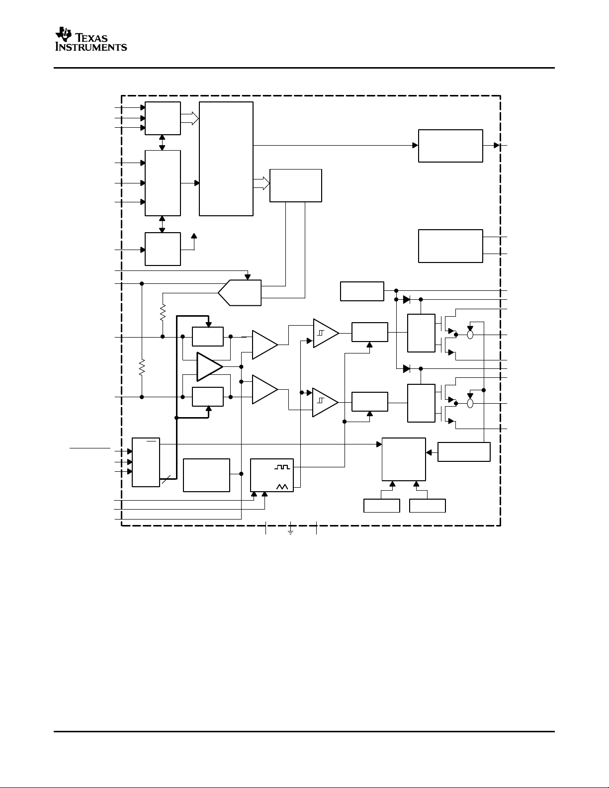
LRCK
1.0 mF
Control
Inputs
DGND
Gain Select
+5V
Channel Select
{
BCK
GAIN0
VCOM
DATA
FORMAT
SCLK
GAIN1
LR_SEL
VDD
SHUTDOWN
VCLAMP
PGND
Shutdown Control
+18V
MUTE
DEMP
ZERO
AVCC
10 mF
{
Zero Input Flag
FLT1
FLT2
22 nF
COSC
AGND
ROSC
VREF
BYPASS
220 pF
1 mF
1 mF
120 kW
0.22 mF
BSN
51 W
OUTN
0.22 mF
BSP
OUTP
51 W
PVCC
Digital Audio
Processor
TPA3200D1
I2S or 16-bit RJ
TAS3103
20-W MONO DIGITAL INPUT AUDIO AMPLIFIER
FEATURES DESCRIPTION
• Digital Interface
– 24-bit Resolution
– Supports I2S and 16-Bit Word
Right-Justified Digital Input Formats
– Multiple Sampling Frequencies:
5 kHz – 200 kHz
– 8x Oversampling Digital Filter
– Soft Mute
• Power Amplifier
– 20-W into an 8- Ω Load from an 18-V Supply
– Efficient Operation Eliminates Need for Heat
Sinks
– Three Selectable, Fixed Gain Settings
– Thermal and Short-Circuit Protection
TPA3200D1
SLOS442A – MAY 2005 – REVISED JULY 2005
The TPA3200D1 is a 20-W (per channel) efficient,
digital audio power amplifier for driving a bridged-tied
speaker. The TPA3200D1 can drive a speaker with
an impedance as low as 4 Ω . The high efficiency of
the TPA3200D1 (85%) eliminates the need for an
external heat sink.
The digital input accepts 16-24 bit data in I2S format
or 16-bit word right-justified. A digital filter performs
an 8x interpolation function. Other features include
soft mute, a zero input detect output flag for power
conscious designs, and power saving shutdown
mode.
PowerPAD is a trademark of Texas Instruments.
PRODUCTION DATA information is current as of publication date.
Products conform to specifications per the terms of the Texas
Instruments standard warranty. Production processing does not
necessarily include testing of all parameters.
Please be aware that an important notice concerning availability, standard warranty, and use in critical applications of Texas
Instruments semiconductor products and disclaimers thereto appears at the end of this data sheet.
Simplified Application Circuit
Copyright © 2005, Texas Instruments Incorporated
Page 2
www.ti.com
TPA3200D1
SLOS442A – MAY 2005 – REVISED JULY 2005
These devices have limited built-in ESD protection. The leads should be shorted together or the device
placed in conductive foam during storage or handling to prevent electrostatic damage to the MOS gates.
AVAILABLE OPTIONS
T
A
–40 ° C to 85 ° C TPA3200D1DCP
(1) The DCP package is available taped and reeled. To order a taped
and reeled part, add the suffix R to the part number (e.g.,
TPA3200D1DCPR).
ABSOLUTE MAXIMUM RATINGS
over operating free-air temperature range (unless otherwise noted)
V
SS
R
L
Vi GAIN0, GAIN1, BCK, SCLK, DATA, LRCK, LR_SEL
T
A
T
J
T
stg
(1) Stresses beyond those listed under absolute maximum ratings may cause permanent damage to the device. These are stress ratings
only, and functional operations of the device at these or any other conditions beyond those indicated under recommended operating
conditions is not implied. Exposure to absolute-maximum-rated conditions for extended periods may affect device reliability.
Supply voltage, VCC, PVCC –0.3 to 21 V
Supply voltage, VDD –0.3 to 6.5 V
Load Impedance ≥ 3.6 Ω
SHUTDOWN – 0.3 to V
FORMAT, MUTE, DEMP
Continuous total power dissipation See Dissipation Rating Table
Operating free-air temperature range –25 to 85 ° C
Operating junction temperature range –25 to 150 ° C
Storage temperature range –65 to 150 ° C
Lead temperature 1.6 mm (1/16 inch) from case for 10 seconds 260 ° C
PACKAGED DEVICE
44-PIN (DCP)
(1)
(1)
TPA3200D1 UNIT
+ 0.3 V
CC
–0.3 to V
+ 0.3 V
DD
DISSIPATION RATINGS
PACKAGE TA≤ 25 ° C DERATING FACTOR TA= 70 ° C TA= 85 ° C
44-pin DCP 4.89 W 39.1 mW/ ° C
(1) Based on a JEDEC high-K PCB with the PowerPAD™ soldered to a thermal land on the printed-circuit board. See the PowerPAD
Thermally Enhanced Package technical brief, literature number SLMA0002. The PowerPAD must be soldered to the PCB.
2
(1/ θJA)
(1)
3.13 W 2.54 W
Page 3
www.ti.com
RECOMMENDED OPERATING CONDITIONS
PARAMETER PIN NAME MIN MAX UNIT
V
SS
V
IH
V
IL
V
IH
V
IL
I
IH
I
IL
V
OH
V
OL
f
OSC
Supply voltage
High-level input voltage 2
Low-level input voltage 0.8
High-level input voltage LR_SEL VDD x 0.7
Low-level input voltage LR_SEL VDD x 0.3
High-level input current
Low-level input current
High-level output voltage IOH= –1 mA, ZERO 2.4
Low-level output voltage IOL= 1 mA, ZERO 0.4
Oscillator frequency 200 300 kHz
SLOS442A – MAY 2005 – REVISED JULY 2005
PVCC, VCC 8 18
VDD 4.5 5.5
SHUTDOWN, GAIN0, GAIN1, BCK, SCLK, DATA,
LRCK, FORMAT, MUTE, DEMP
SHUTDOWN, GAIN0, GAIN1, BCK, SCLK, DATA,
LRCK, FORMAT, MUTE, DEMP
SHUTDOWN: VI= VCC, VCC = 12 V 1
GAIN0, GAIN1, LR_SEL: VI= VDD, VDD = 5 V 1
SCLK, BCK, DATA, LRCK: VI= VDD, VDD = 5 V 10
FORMAT, MUTE, DEMP: VI= VDD, VDD = 5 V 100
SHUTDOWN: VI= 0 V, VCC = 12 V 1
GAIN0, GAIN1, LR_SEL: VI= 0 V, VDD = 5 V 1
BCK, SCLK, DATA, LRCK, FORMAT, MUTE, DEMP:
VI= 0 V, VDD = 5 V
TPA3200D1
V
µA
10
V
ELECTRICAL CHARACTERISTICS
All specifications at TA= 25 ° C, V
PARAMETER TEST CONDITIONS MIN TYP MAX UNIT
POWER SUPPLY REQUIREMENTS
I
DD
DIGITAL FILTER PERFORMANCE
FILTER CHARACTERISTICS
ANALOG FILTER PERFORMANCE
SAMPLING FREQUENCY
fs Sampling frequency 5 200 KHz
DYNAMIC PERFORMANCE
(1) Conditions in 192-kHz operation are system clock = 128 fSand oversampling rate = 64 fSof register 18.
Supply current fS= 96 kHz 25 mA
Pass band ± 0.04 dB 0.454 f
Stop band 0.546 f
Pass-band ripple ± 0.04 dB
Stop-band attenuation Stop band = 0.546 f
Frequency response dB
Channel separation fS= 44.1 KHz, 96 KHz, 192 KHz 100 dB
= 5 V, fS= 44.1 kHz, system clock = 384 fSand 24-bit data, unless otherwise noted
DD
(1)
fS= 44.1 kHz 26 31
fS= 192 kHz 30
s
S
–50 dB
At 20 kHz –0.03
At 44 kHz –0.20
s
3
Page 4
www.ti.com
TPA3200D1
SLOS442A – MAY 2005 – REVISED JULY 2005
FORMAT CHARACTERISTICS
All specifications at TA= 25 ° C, V
PARAMETER TEST CONDITIONS MIN TYP MAX UNIT
Resolution 24 Bits
Data
Audio-data interface format Audio I2S, standard
Audio-data bit length Audio 16–24-bit (I2S), 16-bit (Right-justified)
Audio data format MSB first, 2s complement
System clock frequency 128 fS,192 fS, 256 fS, 384 fS,
ELECTRICAL CHARACTERISTICS
at TA= 25 ° C, PV
|V
| Output offset voltage (measured differentially) MUTE = 2 V AV= 12 dB 100 mV
OS
PSRR Power supply rejection ratio PV
V
5 V regulator voltage IL= 10 mA, V
REF
I
Supply current
CC
I
Supply current shutdown mode SHUTDOWN = 0.8 V 1 2 µA
CC(SD)
Output transistor on resistance (high side and
r
DS(on)
low side)
G Gain GAIN1 = 0.8 V, GAIN0 = 2 V 17.1 18 18.6 dB
= V
CC
= 12 V (unless otherwise noted)
CC
PARAMETER TEST CONDITIONS MIN TYP MAX UNIT
= 5 V, fS= 44.1 kHz, system clock = 384 fSand 24-bit data, unless otherwise noted
DD
512 fS, 768 fS, 1152 f
= 11.5 V to 12.5 V –73 dB
CC
S
= 8 V – 18 V 4.55 4.9 5.45 V
CC
SHUTDOWN = 2.0 V, No load 8 15 mA
SHUTDOWN = VCC, V
RL= 8 Ω
= 18 V, PO = 20 W, 1.3
CC
IO= 0.5 A, TJ= 25 ° C 0.5 0.6 0.7 Ω
GAIN1 = 0.8 V, GAIN0 = 0.8 V 10.9 12 13.1
GAIN1 = 2 V, GAIN0 = 0.8 V 22.9 23.6 24.4
A
OPERATING CHARACTERISTICS
PV
= V
CC
P
O
THD+N Total harmonic distortion plus noise PO= 10 W, RL= 4 Ω f = 20 Hz to 20 kHz 0.2%
B
OM
k
SVR
SNR Signal-to-noise ratio PO= 10 W, RL= 4 Ω 95
V
n
= 12 V, TA= 25 ° C unless otherwise noted
CC
PARAMETER TEST CONDITIONS MIN TYP MAX UNIT
Continuous output power at 10% THD+N f = 1 kHz, RL= 4 Ω 12.8
f = 1 kHz, RL= 8 Ω 9
Continuous output power at 1% THD+N f = 1 kHz, RL= 4 Ω 10.3
f = 1 kHz, RL= 8 Ω 7.5
Maximum output power bandwidth THD = 1% 20 kHz
Supply ripple rejection ratio f = 1 kHz, C
Noise output voltage
C
A-weighted filter Gain = 12 dB
= 1 µF, f = 20 Hz to 22 kHz, 150 µV(rms)
(BYPASS)
(BYPASS)
= 1 µF –60
W
dB
–76.5 dBV
4
Page 5
www.ti.com
Audio
Serial
Port
Serial
Control
Port
4x/8x
Oversampling
Digital
Filter
and
Function
Control
Multi-Level
Delta-Sigma
Modulator
Audio
Serial
Port
System Clock
BCK
LRCK
DATA
FORMAT
MUTE
DEMP
SCLK
DAC and
2:1 Mux
LR_SEL
VCOM
Gain
Adjust
−
+
+
−
Gain
Adjust
FLT1
FLT2
_
+
_
+
_
+
_
+
Deglitch
Logic
Deglitch
Logic
Gate
Drive
Gate
Drive
Clamp
Reference
Short-Circuit
Detect
Start-Up
Protection
Logic
Thermal VCC OK
SD
Gain
SHUTDOWN
GAIN0
GAIN1
2
Biases
and
References
Ramp
Generator
VREF AGND AVCC
VREF AV
CC
Power Supply
Zero Detect
COSC
ROSC
BYPASS
ZERO
VDD
DGND
VCLAMP
BSN
PVCC
OUTN
PGND
BSP
OUTP
PGND
PVCC
Functional Block Diagram
TPA3200D1
SLOS442A – MAY 2005 – REVISED JULY 2005
5
Page 6

www.ti.com
1
BCK
SCLK
2
3
4
5
6
7
8
9
10
11
12
13
14
15
16
17
18
19
20
21
22
44
43
42
41
40
39
38
37
36
35
34
33
32
31
30
29
28
27
26
25
24
23
NC
LRCK
DATA
DGND
VDD
LR_SEL
VDD
DGND
VCOM
GAIN0
GAIN1
SHUTDOWN
PGND
VCLAMP
NC
BSN
PVCC
OUTN
OUTN
PGND
PGND
FORMAT
MUTE
DEMP
DGND
ZERO
DGND
FLT1
FLT2
VCC
VREF
BYPASS
COSC
ROSC
AGND
AGND
BSP
PVCC
OUTP
OUTP
PGND
PGND
TPA3200D1
SLOS442A – MAY 2005 – REVISED JULY 2005
DCP
(TOP VIEW)
6
Page 7
www.ti.com
SLOS442A – MAY 2005 – REVISED JULY 2005
Terminal Functions
TERMINAL
NO. NAME
1 BCK I Bit clock input for audio data
3 DATA I Audio data input
4 LRCK I Left and right channel audio data latch enable input
7 LR_SEL I HIGH: Left channel active
11 GAIN0 I Gain select least significant bit. TTL logic levels with compliance to 5 V.
12 GAIN1 I Gain select most significant bit. TTL logic levels with compliance to 5 V.
13 SHUTDOWN I
5, 9, 38, 40 DGND - Digital ground
6, 8 VDD - Digital power supply (4.5 V – 5.5 V)
15 VCLAMP - Internally generated voltage supply for bootstrap capacitor
17 BSN I/O Bootstrap I/O, negative high-side FET
28 BSP I/O Bootstrap I/O, positive high-side FET
2, 16 NC - No internal connection
31 ROSC I/O I/O for current setting resistor for ramp generator
32 COSC I/O I/O for charge/discharging currents onto capacitor for ramp generator creation
33 BYPASS O Midrail analog reference voltage
34 VREF O Analog 5-V regulated output. Not to be used for powering external circuitry.
35 VCC - High-voltage analog power supply (8 V to 18 V).
19, 20 OUTN O Class-D 1/2-H-bridge negative output
39 ZERO O
41 DEMP I HIGH: 44.1 kHz De-emphasis ON
42 MUTE I HIGH: Mute ON
43 FORMAT I HIGH: 16-bit right justified
44 SCLK I System clock input
18, 27 PVCC - Power supply for H-bridge (8 V to 18 V)
25, 26 OUTP O Class-D 1/2-H-bridge positive output
29, 30 AGND - Analog ground
14, 21, 22, 23, 24 PGND - Power ground for H-bridge
10 VCOM - Midrail digital reference voltage
36 FLT2 I/O
37 FLT1 I/O
Thermal Pad
I/O DESCRIPTION
Select left-channel or right-channel data
LOW: Right channel active
Shutdown signal for IC (low = shutdown, high = operational).
TTL logic levels with compliance to 18 V.
Zero flag output
HIGH: No input present
LOW: Data present at input
This can be used to shutdown the device when no data is present at input.
De-emphasis control.
LOW: 44.1 kHz De-emphasis OFF
Soft mute control
LOW: Mute OFF
Audio data format select
LOW: 16- to 24-bit, I2S format
Noise-filter terminals. Connect capacitor across pins 36 and 37
Connect to AGND and PGND - should be the center point for both grounds.
Internal esistive connection to AGND.
TPA3200D1
7
Page 8
www.ti.com
0.01
10
0.02
0.05
0.1
0.2
0.5
1
2
5
10m 10100m 200m 1 2
Total Hormonic Distortion Plus Noise − %
PO − Output Power − W
20 Hz
1 kHz
10 kHz
VCC = 12 V
RL = 8
Gain = 18 dB
fS = 48 kHz
24−bit, I2S format
0.01
10
0.02
0.05
0.1
0.2
0.5
1
2
5
10m 10100m 200m 1 2
Total Hormonic Distortion Plus Noise − %
PO − Output Power − W
20 Hz
1 kHz
10 kHz
VCC = 12 V
RL = 8
Gain = 23.6 dB
fS = 48 kHz
24−bit, I2S format
0.01
10
0.02
0.05
0.1
0.2
0.5
1
2
5
10m 20100m 200m 1 10
THD+N - T
otal Harmonic Distortion + Noise - %
PO- Output Power - W
10 kHz
1 kHz
R = 4 ,LÙ
Gain = 18 dB,
f = 48 kHz,
s
24-bit, I S format
2
V = 12 V
CC
20 Hz
0.01
10
0.02
0.05
0.1
0.2
0.5
1
2
5
10m
20
100m 200m
1102
Total Hormonic Distortion Plus Noise − %
PO − Output Power − W
20 Hz
1 kHz
10 kHz
VCC = 18 V
RL = 8
Gain = 23.6 dB
fS = 48 kHz
24−bit, I2S format
TPA3200D1
SLOS442A – MAY 2005 – REVISED JULY 2005
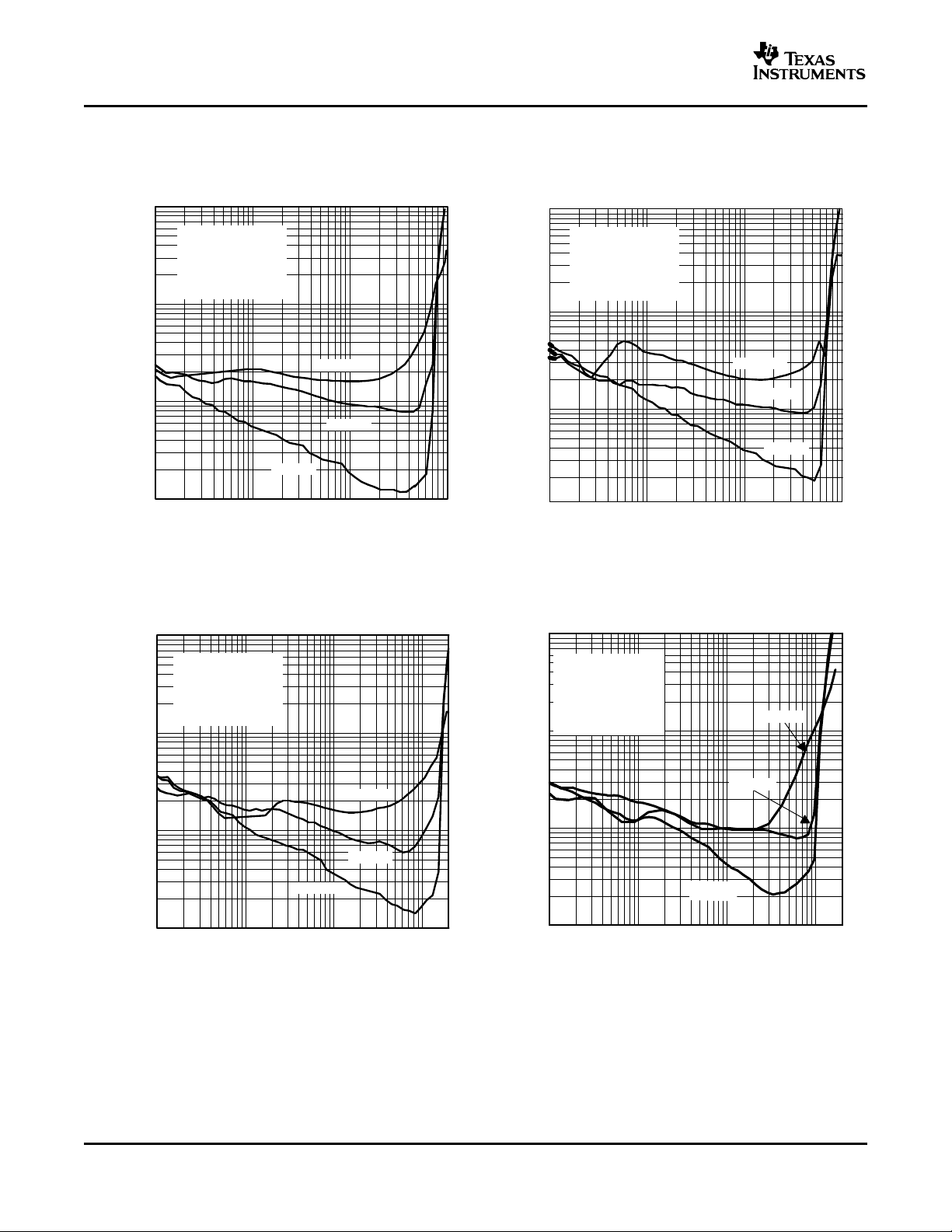
TYPICAL CHARACTERISTICS
Total Harmonic Distortion Plus Noise Total Harmonic Distortion Plus Noise
vs vs
Output Power Output Power
Figure 1. Figure 2.
Harmonic Distortion Plus Noise Total Harmonic Distortion
vs vs
Output Power Power
8
Figure 3. Figure 4.
Page 9
www.ti.com
0.01
20
0.02
0.05
0.1
0.2
0.5
1
2
5
10
20 20k100 200 1k 2k 10k
PO = 1 W
Total Hormonic Distortion Plus Noise − %
f − Frequency − Hz
VCC = 12 V
RL = 8
Gain = 18 dB
fS = 48 kHz
24−bit, I2S format
PO = 5 W
PO = 500 mW
0.01
20
0.02
0.05
0.1
0.2
0.5
1
2
5
10
20 20k100 200 1k 2k 10k
Total Hormonic Distortion Plus Noise − %
f − Frequency − Hz
PO = 500 mW
PO = 1 W
PO = 5 W
VCC = 12 V
RL = 8
Gain = 23.6 dB
fS = 48 kHz
24−bit, I2S format
0.01
20
0.02
0.05
0.1
0.2
0.5
1
2
5
10
20 20k100 200 1k 2k 10k
Total Hormonic Distortion Plus Noise − %
f − Frequency − Hz
PO = 500 mW
PO = 1 W
PO = 5 W
VCC = 18 V
RL = 8
Gain = 18 dB
fS = 48 kHz
24−bit, I2S format
0.01
20
0.02
0.05
0.1
0.2
0.5
1
2
5
10
20 20k100 200 1k 2k 10k
Total Hormonic Distortion Plus Noise − %
f − Frequency − Hz
PO = 500 mW
PO = 1 W
PO = 5 W
VCC = 18 V
RL = 8
Gain = 23.6 dB
fS = 48 kHz
24−bit, I2S format
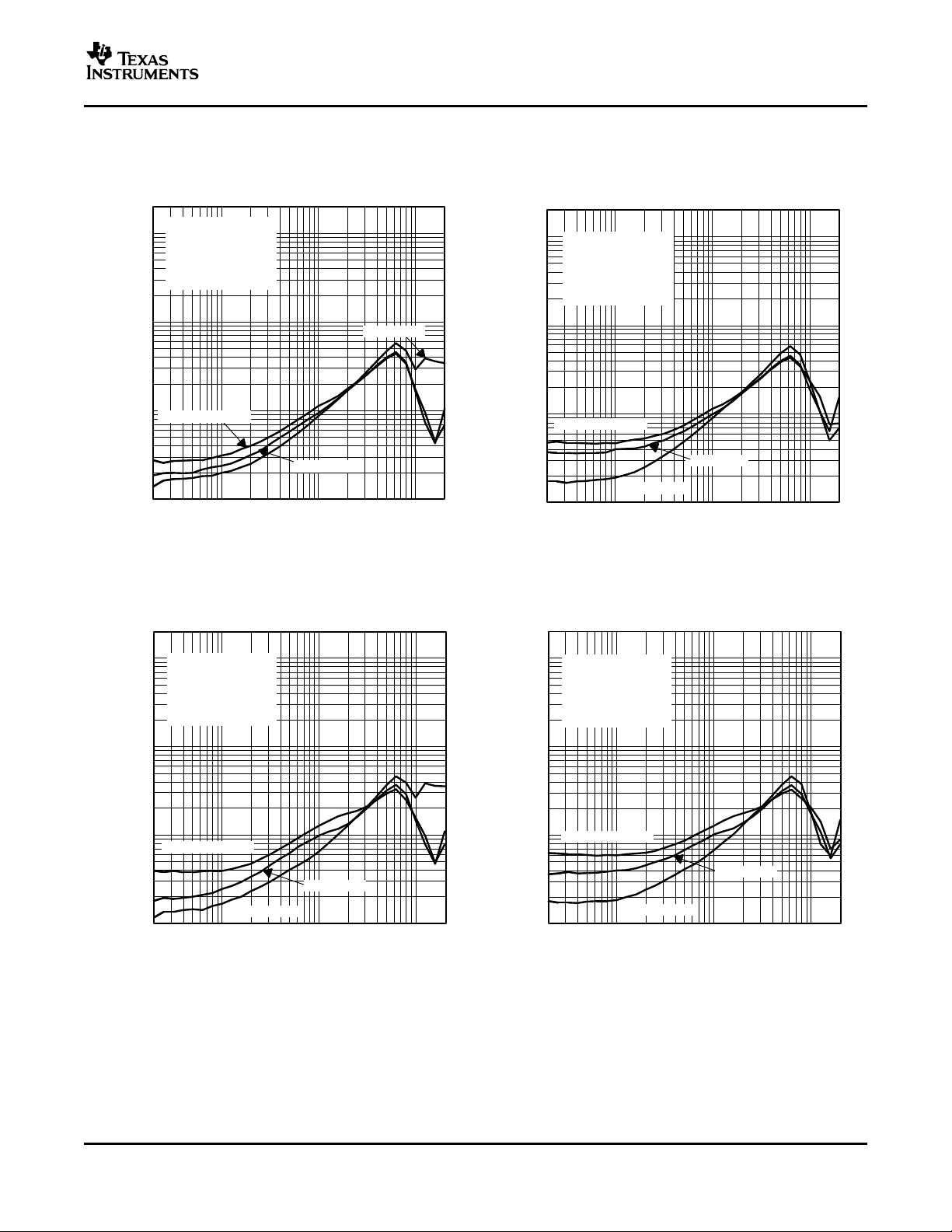
TYPICAL CHARACTERISTICS (continued)
TPA3200D1
SLOS442A – MAY 2005 – REVISED JULY 2005
Total Harmonic Distortion Plus Noise Total Harmonic Distortion Plus Noise
vs vs
Frequency Frequency
Figure 5. Figure 6.
Total Harmonic Distortion Plus Noise Total Harmonic Distortion Plus Noise
vs vs
Frequency Frequency
Figure 7. Figure 8.
9
Page 10

www.ti.com
0.01
10
0.02
0.05
0.1
0.2
0.5
1
2
5
20 20k50 100 200 500 1k 2k 5k 10k
THD + N - Total Harmonic Distortion + Noise - %
f - Frequency - Hz
V = 12 V
CC
R = 4LÙ
Gain = 18 dB
f = 48 kHz
S
24-Bit, I S format
2
P = 2 W
o
P = 200 mW
o
P = 7.5 W
o
−70
−60
−50
−40
−30
−20
−10
0
20 100 1 k 10 k 20 k
f − Frequency − Hz
PSRR − Power Supply Rejecyion Ratio − dB
VCC = 12 V
V
(RIPPLE)
= 200 mV
PP
RL = 8
Gain = 18 dB
0
10
20
30
40
50
60
70
80
90
0 2 4 6 8 10 12 14
PO − Output Power − W
4 Ω
8 Ω
Efficiency − %
VCC = 12 V
5
7
9
11
13
15
17
19
21
3.6 4 5 6 7 8 9 10
VCC = 18 V
VCC = 15 V
VCC = 12 V
TA = 25°C,
10% THD Maximum
ZL − Load Impedance − Ω
− Output Power − WP
O
TPA3200D1
SLOS442A – MAY 2005 – REVISED JULY 2005
TYPICAL CHARACTERISTICS (continued)
Total Harmonic Distortion Power Supply Voltage Rejection Ratio
vs vs
Frequency Frequency
Figure 9. Figure 10.
Efficiency Output Power
vs vs
Output Power Load Impedance
10
Figure 11. Figure 12.
Page 11

www.ti.com
5
7
9
11
13
15
17
19
21
3.6 4 5 6 7 8 9 10
VCC = 18 V
VCC = 15 V
VCC = 12 V
− Maximum Output Power − WP
O
ZL − Load Impedance − Ω
TA = 45°C
5
7
9
11
13
15
17
19
21
3.6 4 5 6 7 8 9 10
VCC = 18 V
VCC = 15 V
VCC = 12 V
− Maximum Output Power − WP
O
ZL − Load Impedance − Ω
TA = 60°C
f – Frequency – kHz
−10
−9
−8
−7
−6
−5
−4
−3
−2
−1
0
0 2 4 6 8 10 12 14 16 18 20
De-emphasis Level – dB
fS = 44.1 kHz
f – Frequency – kHz
−0.5
−0.4
−0.3
−0.2
−0.1
0.0
0.1
0.2
0.3
0.4
0.5
0 2 4 6 8 10 12 14 16 18 20
De-emphasis Error – dB
fS = 44.1 kHz
TYPICAL CHARACTERISTICS (continued)
TPA3200D1
SLOS442A – MAY 2005 – REVISED JULY 2005
Maximum Output Power Maximum Output Power
De-emphasis Level De-emphasis Error
vs vs
Load Impedance Load Impedance
Figure 13. Figure 14.
vs vs
Frequency Frequency
Figure 15. Figure 16.
11
Page 12

www.ti.com
1 mF
1 mF
220 pF
VCC
PGND and DGND
connected at
power supply
Shutdown Control
{
VDD
GAIN0
VCOM
GAIN1
VCC
120 kW
NC
DGND
VDD
LRCK
DGND
BCK
DATA
LR_SEL
VDD
SHUTDOWN
PGND
PGND
VCLAMP
BSN
OUTN
OUTN
PGND
PVCC
NC
0.1 mF
1 mF
51 W
0.22 mF
OUTN
Ferrite
Bead
1 nF
OUTP
Ferrite
Bead
Ferrite
Bead
1 nF
0.22 mF
22 mF
FORMAT
SCLK
COSC
PGND
AGND
BSP
OUTP
OUTP
ROSC
PVCC
AGND
MUTE
DGND
DEMP
DGND
FLT1
ZERO
FLT2
VCC
VREF
BYPASS
PGND
10 mF
10 Fm
22 nF
Gain Control
{
I2S/RJ Clocks
& Data
51 W
}
Control
Inputs
Zero Flag Output
PGND
DGND
1 mF
1 mF
TPA3200D1
SLOS442A – MAY 2005 – REVISED JULY 2005
APPLICATION INFORMATION
12
Figure 17. Typical Application Circuit
Page 13

www.ti.com
t
(SCKH)
t
(SCY)
System Clock (SCK)
t
(SCKL)
2.0 V
0.8 V
H
L
TPA3200D1
SLOS442A – MAY 2005 – REVISED JULY 2005
APPLICATION INFORMATION (continued)
SYSTEM CLOCK INPUT
The TPA3200D1 requires a system clock for operating the digital interpolation filters and multilevel delta-sigma
modulators. The system clock is applied at the SCLK input (pin 44). Table 1 shows examples of system clock
frequencies for common audio sampling rates.
Figure 18 shows the timing requirements for the system clock input. For optimal performance, it is important to
use a clock source with low phase-jitter and noise. TI’s PLL170x family of multiclock generators is an excellent
choice for providing the TPA3200D1 system clock.
Table 1. System Clock Rates for Common Audio Sampling Frequencies
SAMPLE SYSTEM CLOCK FREQUENCY (f
FREQUENCY
8 kHz 1.0240 1.5360 2.0480 3.0720 4.0960 6.1440 9.2160
16 kHz 2.0480 3.0720 4.0960 6.1440 8.1920 12.2880 18.4320
32 kHz 4.0960 6.1440 8.1920 12.2880 16.3840 24.5760 36.8640
44.1 kHz 5.6448 8.4672 11.2896 16.9344 22.5792 33.8688 (1)
48 kHz 6.1440 9.2160 12.2880 18.4320 24.5760 36.8640 (1)
88.2 kHz 11.2896 16.9344 22.5792 33.8688 45.1584 (1) (1)
96 kHz 12.2880 18.4320 24.5760 36.8640 49.1520 (1) (1)
192 kHz 24.5760 36.8640 49.1520 See
(1) This system clock rate is not supported for the given sampling frequency.
128 f
S
192 f
S
256 f
S
384 f
S
(1)
) (MHz)
SCLK
512 f
S
(1) (1) (1)
768 f
S
1152f
S
System clock pulse duration, high t
System clock pulse duration, low t
System clock pulse cycle time t
(1) 1/128 fS, 1/256 fS, 1/384 fS, 1/512 fS, 1/768 fS, or 1/1152 f
AUDIO SERIAL INTERFACE
The audio serial interface for the TPA3200D1 consists of a 3-wire synchronous serial port. It includes LRCK (pin
4), BCK (pin 1), and DATA (pin 3). BCK is the serial audio bit clock, and it is used to clock the serial data present
on DATA into the serial shift register of the audio interface. Serial data is clocked into the TPA3200D1 on the
rising edge of BCK. LRCK is the serial audio left/right word clock. It is used to latch serial data into the internal
registers of the serial audio interface.
Both LRCK and BCK should be synchronous to the system clock. Ideally, it is recommended that LRCK and BCK
be derived from the system clock input, SCK. LRCK is operated at the sampling frequency, fS. BCK can be
operated at 32, 48, or 64 times the sampling frequency for standard and left-justified formats. BCK can be
operated at 48 or 64 times the sampling frequency for the I2S format.
Internal operation of the TPA3200D1 is synchronized with LRCK. Accordingly, internal operation is held when the
sampling rate clock of LRCK is changed or when SCK and/or BCK is interrupted for a 3-bit clock cycle or longer.
If SCK, BCK, and LRCK are provided continuously after this held condition, the internal operation is
re-synchronized automatically in a period of less than 3/f
Figure 18. System Clock Input Timing
PARAMETERS SYMBOL MIN TYP MAX UNITS
(SCKH)
(SCKL)
(SCY)
S
. External resetting is not required.
S
7
7 See
ns
(1)
13
Page 14
www.ti.com
DATA
t
(BCH)
1.4 V
BCK
LRCK
t
(BCL)
t
(LB)
t
(BCY)
t
(DS)
t
(DH)
1.4 V
1.4 V
t
(BL)
TPA3200D1
SLOS442A – MAY 2005 – REVISED JULY 2005
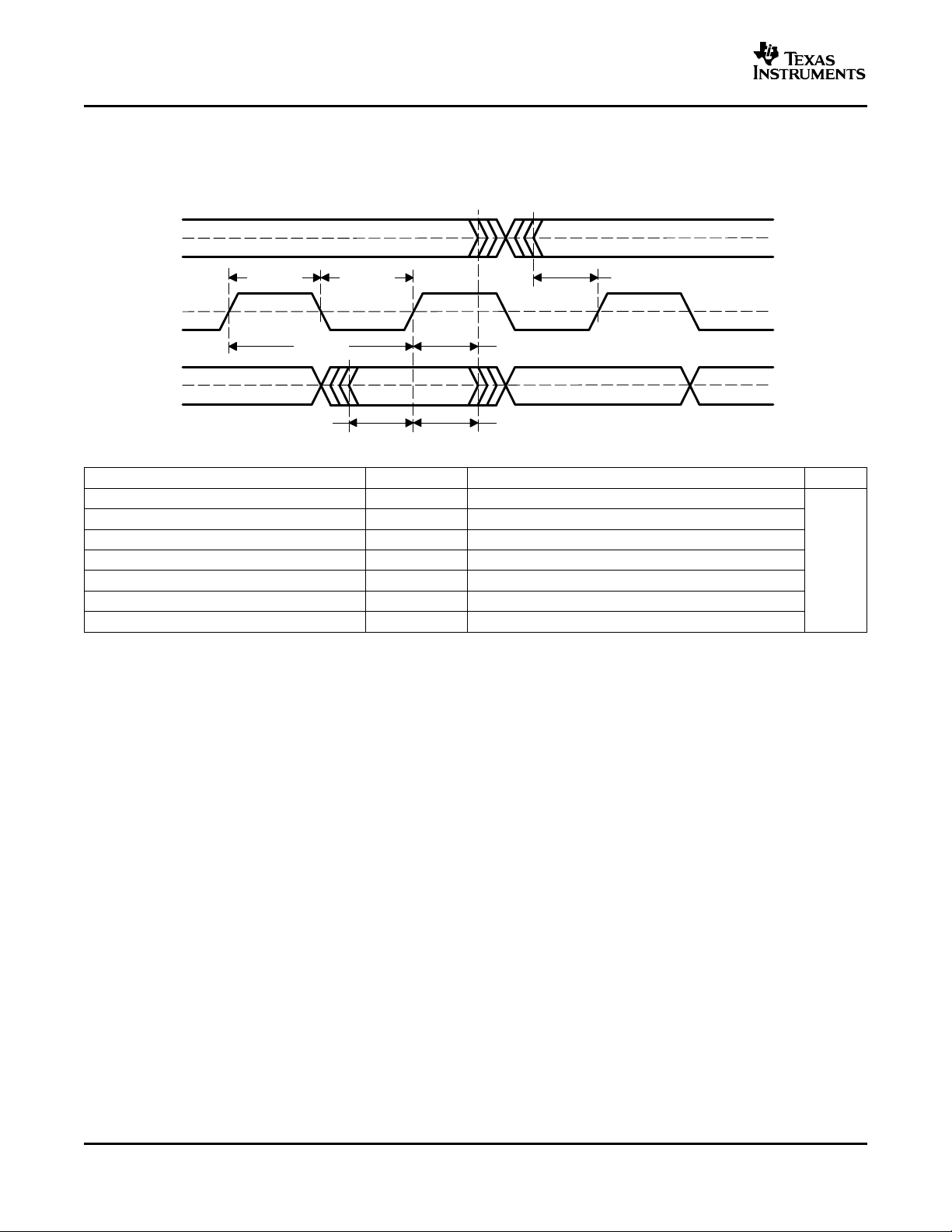
AUDIO DATA FORMATS AND TIMING
The TPA3200D1 supports I2S and 16-bit-word right-justified. The data formats are shown in Figure 20 . Data
formats are selected using the FORMAT pin on the TPA3200D1. All formats require binary 2s-complement,
MSB-first audio data. Figure 19 shows a detailed timing diagram for the serial audio interface.
Figure 19. Audio Interface Timing
PARAMETERS SYMBOL MIN TYP MAX UNITS
BCK pulse cycle time t
BCK high-level time t
BCK low-level time t
BCK rising edge to LRCK edge t
LRCK falling edge to BCK rising edge t
DATA setup time t
DATA hold time t
(BCY)
(BCH)
(BCL)
(BL)
(LB)
(DS)
(DH)
(1) fSis the sampling frequency (e.g., 44.1 kHz, 48 kHz, 96 kHz, etc.).
1/(32 fS), 1/(48 fS), 1/(64 fS)
(1)
35
35
10 ns
10
10
10
14
Page 15

www.ti.com
LRCK
(2) I2S Data Format; L-Channel = LOW, R-Channel = HIGH
1/f
S
(= 32 fS, 48 fS, or 64 fS)
(1) 16-Bit-Word Right Justified
1/f
S
(= 48 fS or 64 fS)
MSB LSB
16-Bit Right-Justified, BCK = 32 f
S
16-Bit Right-Justified, BCK = 48 fS or 64 f
S
MSB LSB
L-Channel R-Channel
BCK
DATA 14 15 16 1 2 3 14 15 16
14 15 16 1 2 3 14 15 16DATA
MSB LSB
MSB LSB
1 2 3 14 15 16
1 2 3 14 15 16
L-Channel R-ChannelLRCK
BCK
DATA
1 2 3 1 2
MSB
N–2NN–1
LSB
1 2 3
MSB
N–2NN–1
LSB
TPA3200D1
SLOS442A – MAY 2005 – REVISED JULY 2005
Figure 20. Audio Data Input Formats
ZERO FLAG
ZERO (pin 39) is the L-channel and R-channel common zero flag pin. If the data for L-channel and R-channel
remains at a 0 level for 1024 sampling periods (or LRCK clock periods), the ZERO flag output is set to a logic 1
state.
The ZERO-pin output can be inverted using a standard logic gate or transistor, and connected to the
SHUTDOWN terminal (pin 13). This places the TPA3200D1 into a low-current state, conserving power, and
disables the switching outputs.
15
Page 16

www.ti.com
TPA3200D1
SLOS442A – MAY 2005 – REVISED JULY 2005
REGISTER CONTROL
The digital functions of the TPA3200D1 are controlled by 4 terminals. Table 2 shows selectable data formats,
Table 3 shows de-emphasis control, Table 4 shows mute control, and Table 5 shows channel-output select.
Table 2. Data Format Select
FMT (PIN 43) DATA FORMAT
LOW 16- to 24-bit, I2S format
HIGH 16-bit right-justified
Table 3. De-Emphasis Control
DEMP (PIN 41 ) DE-EMPHASIS FUNCTION
LOW 44.1 kHz de-emphasis OFF
HIGH 44.1 kHz de-emphasis ON
Table 4. Mute Control
MUTE (PIN 42 ) MUTE
LOW Mute OFF
HIGH Mute ON
Table 5. Channel Output Select
LR_SEL (PIN 7 ) ACTIVE CHANNEL
LOW Right
HIGH Left
(1) A digital data stream consists of two channels of data. In an I2S or
right-justified data stream, the left-channel data precedes the
right-channel data (See Figure 20 ). The LR_SEL input selects the
channel to send to the mono output.
(1)
OVERSAMPLING RATE CONTROL
The TPA3200D1 automatically controls the oversampling rate of the delta-sigma D/A converters with the system
clock rate. The oversampling rate is set to 64× oversampling with every system clock and sampling frequency.
VCOM OUTPUT
One unbuffered common-mode voltage output pin, VCOM (pin 10) is brought out for decoupling purposes. This
pin is nominally biased to a dc voltage level equal to 0.5 × V
. This pin cannot be used to bias external circuits.
DD
16
Page 17

www.ti.com
0 V
−12 V
+12 V
Current
OUTP
Differential Voltage
Across Load
OUTN
TPA3200D1
SLOS442A – MAY 2005 – REVISED JULY 2005
CLASS-D OPERATION
This section focuses on the class-D operation of the TPA3200D1.
Traditional Class-D Modulation Scheme
The traditional class-D modulation scheme, which is used in the TPA032D0x family, has a differential output
where each output is 180 degrees out of phase and changes from ground to the supply voltage, VCC. Therefore,
the differential pre-filtered output varies between positive and negative V
0 V across the load. The traditional class-D modulation scheme with voltage and current waveforms is shown in
Figure 31. Note that even at an average of 0 V across the load (50% duty cycle), the current to the load is high,
causing high loss, thus causing a high supply current.
, where filtered 50% duty cycle yields
CC
Figure 21. Traditional Class-D Modulation Scheme’s Output Voltage and Current Waveforms Into an
Inductive Load With No Input
17
Page 18

www.ti.com
0 V
−12 V
+12 V
Current
OUTP
OUTN
Differential
Voltage
Across
Load
0 V
−12 V
+12 V
Current
OUTP
OUTN
Differential
Voltage
Across
Load
Output = 0 V
Output > 0 V
TPA3200D1
SLOS442A – MAY 2005 – REVISED JULY 2005
TPA3200D1 Modulation Scheme
The TPA3200D1 uses a modulation scheme that still has each output switching from ground to V
OUTP and OUTN are now in phase with each other with no input. The duty cycle of OUTP is greater than 50%
and OUTN is less than 50% for positive output voltages. The duty cycle of OUTP is less than 50% and OUTN is
greater than 50% for negative output voltages. The voltage across the load is 0 V throughout most of the
switching period, greatly reducing the switching current, which reduces any I2R losses in the load. (See
Figure 22 .)
. However,
CC
18
Figure 22. The TPA3200D1 Output Voltage and Current Waveforms Into an Inductive Load
Page 19

www.ti.com
5
7
9
11
13
15
17
19
21
3.6 4 5 6 7 8 9 10
VCC = 18 V
VCC = 15 V
VCC = 12 V
TA = 25°C,
10% THD Maximum
ZL − Load Impedance − Ω
− Output Power − W
MAXIMUM OUTPUT POWER
vs
LOAD IMPEDANCE
P
O
P
O(10% THD)
P
O(1% THD)
1.25
TPA3200D1
SLOS442A – MAY 2005 – REVISED JULY 2005
Maximum Allowable Output Power (Safe Operating Area)
The TPA3200D1 can drive load impedances as low as 3.6 Ω from power supply voltages ranging from 8 V to 18
V. To prevent device failure, however, the output power of the TPA3200D1 must be limited. Figure 23 shows the
maximum allowable output power versus load impedance for three power supply voltages at an ambient
temperature of 25°C.
Figure 23. Output Power
Driving The Output Into Clipping
The output of the TPA3200D1 may be driven into clipping to attain a higher output power than is possible with no
distortion. Clipping is typically quantified by a THD measurement of 10%. The amount of additional power into
the load may be calculated with Equation 1 .
For example, consider an application in which the TPA3200D1 drives an 8- Ω speaker from an 18-V power
supply. The maximum output power with no distortion (less than 1% THD) is 16 W, which corresponds to a
maximum peak output voltage of 16 V. For the same output voltage level driven into clipping (10% THD), the
output power is increased to 20 W.
Output Filter Considerations
A ferrite bead filter (shown in Figure 24 ) should be used in order to pass FCC and/or CE radiated emissions
specifications and if a frequency sensitive circuit operating higher than 1 MHz is nearby. The ferrite filter reduces
EMI around 1 MHz and higher (FCC and CE only test radiated emissions greater than 30 MHz). When selecting
a ferrite bead, choose one with high impedance at high frequencies, but very low impedance at low frequencies.
Use an additional LC output filter if there are low frequency (<1 MHz) EMI sensitive circuits and/or there are long
wires (greater than 11 inches) from the amplifier to the speaker, as shown in Figure 25 and Figure 26 .
(1)
19
Page 20

www.ti.com
1 nF
Ferrite
Chip Bead
OUTP
OUTN
Ferrite
Chip Bead
1 nF
4 or GreaterW
0.22 µF
15 µH
15 µH
OUTP
OUTN
4 Ω
Ferrite
Chip Bead
Ferrite
Chip Bead
1 nF
1 nF
0.22 µF
1 µF
0.1 µF
0.1 µF
33 µH
33 µH
OUTP
OUTN
8 Ω
Ferrite
Chip Bead
Ferrite
Chip Bead
1 nF
1 nF
0.47 µF
TPA3200D1
SLOS442A – MAY 2005 – REVISED JULY 2005
Figure 24. Typical Ferrite Chip Bead Filter (Chip bead example: Fair-Rite 2512067007Y3)
Figure 25. Typical LC Output Filter for 4- Ω Speaker, Cutoff Frequency of 41 kHz
Figure 26. Typical LC Output Filter for 8- Ω Speaker, Cutoff Frequency of 41 kHz
SHORT-CIRCUIT PROTECTION
The TPA3200D1 has short circuit protection circuitry on the outputs that prevents damage to the device during
output-to-output shorts, output-to-GND shorts, and output-to-V
outputs, the part immediately disables the output drive and enters into shutdown mode. This is a latched fault
and must be reset by cycling the voltage on the SHUTDOWN pin to a logic low and back to the logic high state
for normal operation. This will clear the short-circuit flag and allow for normal operation if the short was removed.
If the short was not removed, the protection circuitry will again activate.
Two Schottky diodes are required to provide short-circuit protection. The diodes should be placed as close to the
TPA3200D1 as possible, with the anodes connected to PGND and the cathodes connected to OUTP and OUTN
as shown in the application circuit schematic. The diodes should have a forward voltage rating of 0.5 V at a
minimum of 1 A output current and a dc blocking voltage rating of at least 30 V. The diodes must also be rated to
operate at a junction temperature of 150°C.
If short-circuit protection is not required, the Schottky diodes may be omitted.
20
shorts. When a short-circuit is detected on the
CC
Page 21

www.ti.com
T
Amax
T
Jmax
JAPDissipated
where : T
Jmax
150C
JA
1
deratingfactor
1
0.0391
25.6C
Efficiency 85% for an 8− load
P
Dissipated
P
O(average)
1
Efficiency
1
Efficiency 75% for an 4− load
P
Dissipated
20 W
1
0.85
1 3.53 W
T
Amax
150C (25.6CW 1.76 W) 59.6C
TPA3200D1
SLOS442A – MAY 2005 – REVISED JULY 2005
THERMAL PROTECTION
Thermal protection on the TPA3200D1 prevents damage to the device when the internal die temperature
exceeds 150°C. There is a ±15°C tolerance on this trip point from device to device. Once the die temperature
exceeds the thermal set point, the device enters into the shutdown state and the outputs are disabled. This is not
a latched fault. The thermal fault is cleared once the temperature of the die is reduced by 15°C. The device
begins normal operation at this point with no external system interaction.
THERMAL CONSIDERATIONS: OUTPUT POWER AND MAXIMUM AMBIENT TEMPERATURE
To calculate the maximum ambient temperature, Equation 2 is used:
The derating factor for the 44-pin DCP package is given in the dissipation rating table.
To estimate the power dissipation, Equation 3 is used:
(2)
Example. What is the maximum ambient temperature for an application that requires the TPA3200D1 to drive
20 W into an 8- Ω speaker?
This calculation shows that the TPA3200D1 can drive 20 W of RMS power into an 8- Ω speaker up to a maximum
ambient temperature rating of 60°C.
GAIN SETTING VIA GAIN0 AND GAIN1 INPUTS
The gain of the TPA3200D1 is set by two input terminals, GAIN0 and GAIN1. See Table 6 .
Table 6. Gain Settings
AMPLIFIER GAIN Output Voltage with Full Scale Input
GAIN1 GAIN0
0 0 12 5.63
0 1 18 11.23
1 0 23.6 21.4
1 1 Reserved Reserved
(1) Output clipping with V
= 18 V
CC
(dB) and V
TYP TYP
=5 V (V
DD
)
RMS
(1)
(3)
(4)
21
Page 22

www.ti.com
f
s
6.6
R
OSCCOSC
TPA3200D1
SLOS442A – MAY 2005 – REVISED JULY 2005
The typical output voltage, measured across the load, is also given in Table 6 at each of the gain steps. This is
the expected voltage with a full scale input signal applied at the digital inputs and V
proportionally with a lower or higher V
. For example, if V
DD
= 4.5 V, scale the results in Table 6 by 4.5/5, or
DD
0.9.
The differential offset voltage, measured across the speaker outputs, increases as the gain is increased. For the
lowest offset voltage, specified in the electrical characteristics table, set the gain at the lowest step, 12 dB.
POWER SUPPLY DECOUPLING
The TPA3200D1 is a high-performance CMOS audio amplifier that requires adequate power supply decoupling
to ensure the output total harmonic distortion (THD) is as low as possible. Power supply decoupling also
prevents oscillations for long lead lengths between the amplifier and the speaker. The optimum decoupling is
achieved by using two capacitors of different types that target different types of noise on the power supply leads.
For higher frequency transients, spikes, or digital hash on the line, a good low equivalent-series-resistance (ESR)
ceramic capacitor, typically 1 µF placed as close as possible to the device V
lower-frequency noise signals, a larger aluminum electrolytic capacitor of 10 µF or greater placed near the audio
power amplifier is recommended.
BSN AND BSP CAPACITORS
The full H-bridge output stage uses only NMOS transistors. It therefore requires bootstrap capacitors for the high
side of each output to turn on correctly. A 0.22-µF ceramic capacitor, rated for at least 25 V, must be connected
from each output to its corresponding bootstrap input. Specifically, one 0.22-µF capacitor must be connected
from OUTP to BSP, and one 0.22-µF capacitor must be connected from OUTN to BSN.
= 5 V. This voltage scales
DD
lead works best. For filtering
CC
BSN AND BSP RESISTORS
To limit the current when charging the bootstrap capacitors, a resistor with a value of approximately 50 Ω
(+/–10% maximum) must be placed in series with each bootstrap capacitor. The current will be limited to less
than 500 µA.
VCLAMP CAPACITOR
To ensure that the maximum gate-to-source voltage for the NMOS output transistors is not exceeded, an internal
regulator clamps the gate voltage. A 1-µF capacitor must be connected from VCLAMP (pin 15) to ground. This
capacitor must have a rating of V
or more. The voltage at VCLAMP (pin 15) varies with V
CC
and may not be
CC
used for powering any other circuitry.
MIDRAIL BYPASS CAPACITOR
The midrail bypass capacitor is the most critical capacitor and serves several important functions. During start-up
or recovery from shutdown mode, C
(BYPASS)
determines the rate at which the amplifier starts up. The second
function is to reduce noise produced by the power supply caused by coupling into the output drive signal. This
noise is from the midrail generation circuit internal to the amplifier, which appears as degraded PSRR and
THD+N.
VREF DECOUPLING CAPACITOR
The VREF terminal (pin 34) is the output of an internally-generated 5-V supply, used for the oscillator and gain
setting logic. It requires a 0.1-µF to 1-µF capacitor to ground to keep the regulator stable. The regulator may not
be used to power any additional circuitry.
SWITCHING FREQUENCY
The switching frequency is determined using the values of the components connected to ROSC (pin 31) and
COSC (pin 32) and may be calculated using Equation 5 :
(5)
The frequency may be varied from 225 kHz to 275 kHz by adjusting the values chosen for ROSC and COSC.
22
Page 23

www.ti.com
TPA3200D1
SLOS442A – MAY 2005 – REVISED JULY 2005
SHUTDOWN OPERATION
The TPA3200D1 employs a shutdown mode of operation designed to reduce supply current (I
minimum level during periods of non-use for battery-power conservation. The SHUTDOWN input terminal should
be held high during normal operation when the amplifier is in use. Pulling SHUTDOWN low causes the outputs to
mute and the amplifier to enter a low-current state, I
CC(SD)
= 1 µA. SHUTDOWN should never be left
unconnected, because amplifier operation would be unpredictable.
Ideally, the device should be held in shutdown when the system powers up and brought out of shutdown once
any digital circuitry has settled. However, if SHUTDOWN is to be left unused, the terminal may be connected
directly to V
.
CC
USING LOW-ESR CAPACITORS
Low-ESR capacitors are recommended throughout this application section. A real (as opposed to ideal) capacitor
can be modeled simply as a resistor in series with an ideal capacitor. The voltage drop across this resistor
minimizes the beneficial effects of the capacitor in the circuit. The lower the equivalent value of this resistance
the more the real capacitor behaves like an ideal capacitor.
A metalized polyester capacitor is recommended for the capacitor placed in parallel across the FLT1 and FLT2
inputs. This ensures the best noise performance.
PRINTED-CIRCUIT BOARD (PCB) LAYOUT
Because the TPA3200D1 is a class-D amplifier that switches at a high frequency, the layout of the printed-circuit
board (PCB) should be optimized according to the following guidelines for the best possible performance.
• Decoupling capacitors — The high-frequency 1-µF decoupling capacitors should be placed as close to the
PVCC (pin 18 and pin 27) and VCC (pin 35) terminals as possible. The BYPASS (pin 33) capacitor, VREF
(pin 34) capacitor, and VCLAMP (pin 15) capacitor should also be placed as close to the device as possible.
The large (10 µF or greater) bulk power supply decoupling capacitor should be placed near the TPA3200D1
at the PVCC terminals.
• Grounding — The VCC (pin 35) decoupling capacitor, VREF (pin 34) capacitor, BYPASS (pin 33) capacitor,
COSC (pin 32) capacitor, and ROSC (pin 31) resistor should each be grounded to analog ground (AGND,
pin 29 and pin 30). The PVCC (pin 18 and pin 27) decoupling capacitors should each be grounded to power
ground (PGND pins 14, 21, 22, 23, and 24). Analog ground and power ground may be connected at the
PowerPAD, which should be used as a central ground connection, or star ground, for the TPA3200D1.
DGND (pins 5, 9, 38, and 40) should be connected to PGND, and AGND at the power supply through a
ferrite bead. Connect the VDD (pins 6 and 8) decoupling capacitor to DGND. This pattern separates the
digital power-switching currents and digital input currents, and prevents interference between them.
• Digital input signal routing — The SCLK, BCK, LRCK, and DATA input are sensitive, high-frequency signals
that should be shielded by a clean GND layer to avoid interference. For a 2-layer PCB, shield the signals on
the bottom layer with a plane connected to DGND. On the top layer, route DGND closely around these
signals.
• Output filter — The ferrite filter (Figure 24 ) should be placed as close to the output terminals (pins 19, 20, 25,
and 26) as possible for the best EMI performance. The LC filter (Figure 25 and Figure 26 ) should be placed
closest to the output and followed by a ferrite-bead filter. The capacitors used in both the ferrite and LC filters
should be grounded to power ground.
• PowerPAD — The PowerPAD must be soldered to the PCB for proper thermal performance and optimal
reliability. The dimensions of the PowerPAD thermal land on the PCB should be 3.5 mm by 9.5 mm. Three
rows of solid vias (six vias per row, 0.3302 mm or 13 mils diameter) should be equally spaced underneath
the thermal land. The vias should connect to a solid copper plane, either on an internal layer or on the
bottom layer of the PCB. The vias must be solid vias, not thermal relief or webbed vias. For additional
information, see the PowerPAD Thermally Enhanced Package technical brief, TI literature number SLMA002 .
For an example layout, see the TPA3200D1 Evaluation Module (TPA3200D1EVM) User Manual, TI literature
number SLOU173 . Both the EVM user manual and the PowerPAD application note are available on the TI web
site at http://www.ti.com.
) to the absolute
CC
23
Page 24

PACKAGE OPTION ADDENDUM
www.ti.com
11-Apr-2013
PACKAGING INFORMATION
Orderable Device Status
TPA3200D1DCP NRND HTSSOP DCP 44 40 Green (RoHS
TPA3200D1DCPG4 NRND HTSSOP DCP 44 40 Green (RoHS
TPA3200D1DCPR NRND HTSSOP DCP 44 2000 Green (RoHS
TPA3200D1DCPRG4 NRND HTSSOP DCP 44 2000 Green (RoHS
(1)
The marketing status values are defined as follows:
ACTIVE: Product device recommended for new designs.
LIFEBUY: TI has announced that the device will be discontinued, and a lifetime-buy period is in effect.
NRND: Not recommended for new designs. Device is in production to support existing customers, but TI does not recommend using this part in a new design.
PREVIEW: Device has been announced but is not in production. Samples may or may not be available.
OBSOLETE: TI has discontinued the production of the device.
Package Type Package
(1)
Drawing
Pins Package
Qty
Eco Plan
(2)
& no Sb/Br)
& no Sb/Br)
& no Sb/Br)
& no Sb/Br)
Lead/Ball Finish MSL Peak Temp
(3)
CU NIPDAU Level-1-260C-UNLIM -40 to 85 TPA3200D1
CU NIPDAU Level-1-260C-UNLIM -40 to 85 TPA3200D1
CU NIPDAU Level-1-260C-UNLIM -40 to 85 TPA3200D1
CU NIPDAU Level-1-260C-UNLIM -40 to 85 TPA3200D1
Op Temp (°C) Top-Side Markings
(4)
(2)
Eco Plan - The planned eco-friendly classification: Pb-Free (RoHS), Pb-Free (RoHS Exempt), or Green (RoHS & no Sb/Br) - please check http://www.ti.com/productcontent for the latest availability
information and additional product content details.
TBD: The Pb-Free/Green conversion plan has not been defined.
Pb-Free (RoHS): TI's terms "Lead-Free" or "Pb-Free" mean semiconductor products that are compatible with the current RoHS requirements for all 6 substances, including the requirement that
lead not exceed 0.1% by weight in homogeneous materials. Where designed to be soldered at high temperatures, TI Pb-Free products are suitable for use in specified lead-free processes.
Pb-Free (RoHS Exempt): This component has a RoHS exemption for either 1) lead-based flip-chip solder bumps used between the die and package, or 2) lead-based die adhesive used between
the die and leadframe. The component is otherwise considered Pb-Free (RoHS compatible) as defined above.
Green (RoHS & no Sb/Br): TI defines "Green" to mean Pb-Free (RoHS compatible), and free of Bromine (Br) and Antimony (Sb) based flame retardants (Br or Sb do not exceed 0.1% by weight
in homogeneous material)
(3)
MSL, Peak Temp. -- The Moisture Sensitivity Level rating according to the JEDEC industry standard classifications, and peak solder temperature.
(4)
Multiple Top-Side Markings will be inside parentheses. Only one Top-Side Marking contained in parentheses and separated by a "~" will appear on a device. If a line is indented then it is a
continuation of the previous line and the two combined represent the entire Top-Side Marking for that device.
Important Information and Disclaimer:The information provided on this page represents TI's knowledge and belief as of the date that it is provided. TI bases its knowledge and belief on information
provided by third parties, and makes no representation or warranty as to the accuracy of such information. Efforts are underway to better integrate information from third parties. TI has taken and
continues to take reasonable steps to provide representative and accurate information but may not have conducted destructive testing or chemical analysis on incoming materials and chemicals.
TI and TI suppliers consider certain information to be proprietary, and thus CAS numbers and other limited information may not be available for release.
In no event shall TI's liability arising out of such information exceed the total purchase price of the TI part(s) at issue in this document sold by TI to Customer on an annual basis.
Samples
Addendum-Page 1
Page 25

PACKAGE OPTION ADDENDUM
www.ti.com
11-Apr-2013
Addendum-Page 2
Page 26

PACKAGE MATERIALS INFORMATION
www.ti.com 26-Jan-2013
TAPE AND REEL INFORMATION
*All dimensions are nominal
Device Package
Type
TPA3200D1DCPR HTSSOP DCP 44 2000 330.0 24.4 6.8 11.7 1.6 12.0 24.0 Q1
Package
Drawing
Pins SPQ Reel
Diameter
(mm)
Reel
Width
W1 (mm)
A0
(mm)B0(mm)K0(mm)P1(mm)W(mm)
Pin1
Quadrant
Pack Materials-Page 1
Page 27

PACKAGE MATERIALS INFORMATION
www.ti.com 26-Jan-2013
*All dimensions are nominal
Device Package Type Package Drawing Pins SPQ Length (mm) Width (mm) Height (mm)
TPA3200D1DCPR HTSSOP DCP 44 2000 367.0 367.0 45.0
Pack Materials-Page 2
Page 28

Page 29

Page 30

IMPORTANT NOTICE
Texas Instruments Incorporated and its subsidiaries (TI) reserve the right to make corrections, enhancements, improvements and other
changes to its semiconductor products and services per JESD46, latest issue, and to discontinue any product or service per JESD48, latest
issue. Buyers should obtain the latest relevant information before placing orders and should verify that such information is current and
complete. All semiconductor products (also referred to herein as “components”) are sold subject to TI’s terms and conditions of sale
supplied at the time of order acknowledgment.
TI warrants performance of its components to the specifications applicable at the time of sale, in accordance with the warranty in TI’s terms
and conditions of sale of semiconductor products. Testing and other quality control techniques are used to the extent TI deems necessary
to support this warranty. Except where mandated by applicable law, testing of all parameters of each component is not necessarily
performed.
TI assumes no liability for applications assistance or the design of Buyers’ products. Buyers are responsible for their products and
applications using TI components. To minimize the risks associated with Buyers’ products and applications, Buyers should provide
adequate design and operating safeguards.
TI does not warrant or represent that any license, either express or implied, is granted under any patent right, copyright, mask work right, or
other intellectual property right relating to any combination, machine, or process in which TI components or services are used. Information
published by TI regarding third-party products or services does not constitute a license to use such products or services or a warranty or
endorsement thereof. Use of such information may require a license from a third party under the patents or other intellectual property of the
third party, or a license from TI under the patents or other intellectual property of TI.
Reproduction of significant portions of TI information in TI data books or data sheets is permissible only if reproduction is without alteration
and is accompanied by all associated warranties, conditions, limitations, and notices. TI is not responsible or liable for such altered
documentation. Information of third parties may be subject to additional restrictions.
Resale of TI components or services with statements different from or beyond the parameters stated by TI for that component or service
voids all express and any implied warranties for the associated TI component or service and is an unfair and deceptive business practice.
TI is not responsible or liable for any such statements.
Buyer acknowledges and agrees that it is solely responsible for compliance with all legal, regulatory and safety-related requirements
concerning its products, and any use of TI components in its applications, notwithstanding any applications-related information or support
that may be provided by TI. Buyer represents and agrees that it has all the necessary expertise to create and implement safeguards which
anticipate dangerous consequences of failures, monitor failures and their consequences, lessen the likelihood of failures that might cause
harm and take appropriate remedial actions. Buyer will fully indemnify TI and its representatives against any damages arising out of the use
of any TI components in safety-critical applications.
In some cases, TI components may be promoted specifically to facilitate safety-related applications. With such components, TI’s goal is to
help enable customers to design and create their own end-product solutions that meet applicable functional safety standards and
requirements. Nonetheless, such components are subject to these terms.
No TI components are authorized for use in FDA Class III (or similar life-critical medical equipment) unless authorized officers of the parties
have executed a special agreement specifically governing such use.
Only those TI components which TI has specifically designated as military grade or “enhanced plastic” are designed and intended for use in
military/aerospace applications or environments. Buyer acknowledges and agrees that any military or aerospace use of TI components
which have not been so designated is solely at the Buyer's risk, and that Buyer is solely responsible for compliance with all legal and
regulatory requirements in connection with such use.
TI has specifically designated certain components as meeting ISO/TS16949 requirements, mainly for automotive use. In any case of use of
non-designated products, TI will not be responsible for any failure to meet ISO/TS16949.
Products Applications
Audio www.ti.com/audio Automotive and Transportation www.ti.com/automotive
Amplifiers amplifier.ti.com Communications and Telecom www.ti.com/communications
Data Converters dataconverter.ti.com Computers and Peripherals www.ti.com/computers
DLP® Products www.dlp.com Consumer Electronics www.ti.com/consumer-apps
DSP dsp.ti.com Energy and Lighting www.ti.com/energy
Clocks and Timers www.ti.com/clocks Industrial www.ti.com/industrial
Interface interface.ti.com Medical www.ti.com/medical
Logic logic.ti.com Security www.ti.com/security
Power Mgmt power.ti.com Space, Avionics and Defense www.ti.com/space-avionics-defense
Microcontrollers microcontroller.ti.com Video and Imaging www.ti.com/video
RFID www.ti-rfid.com
OMAP Applications Processors www.ti.com/omap TI E2E Community e2e.ti.com
Wireless Connectivity www.ti.com/wirelessconnectivity
Mailing Address: Texas Instruments, Post Office Box 655303, Dallas, Texas 75265
Copyright © 2013, Texas Instruments Incorporated
 Loading...