

Page 1
1 Fm
SD
MuteControl
PVCCL
TPA3120D2
TPA3120D2
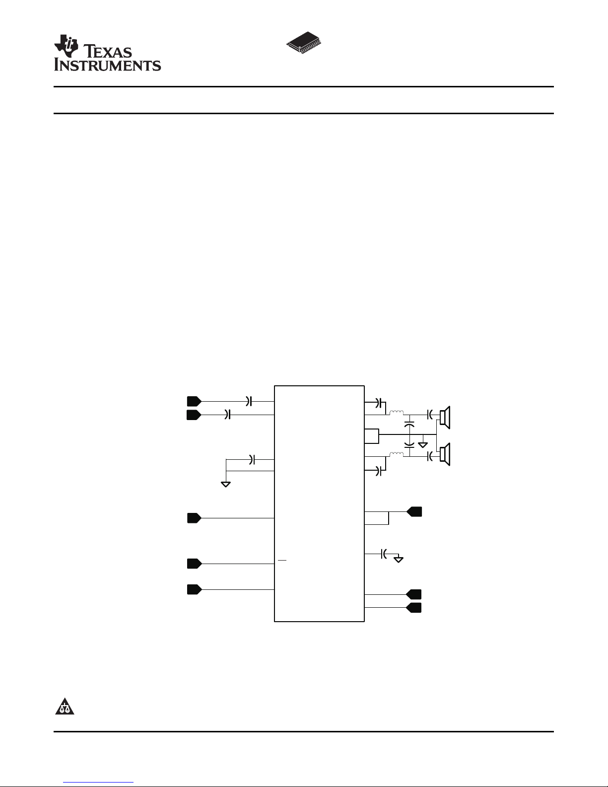
SIMPLIFIED APPLICATIONCIRCUIT
PVCCR
VCLAMP
GAIN1
BYPASS
1 Fm
1 Fm
0.22 Fm
AGND
LeftChannel
RightChannel
10Vto30V
10Vto30V
}
4-StepGain
Control
Shutdown
Control
LIN
RIN
BSR
BSL
PGNDR
PGNDL
0.22 Fm
22 Hm
22 Hm
0.68 Fm
470 Fm
0.68 Fm
1 Fm
470 Fm
GAIN0
AVCC
MUTE
ROUT
LOUT
TPA3120D2
www.ti.com
SLOS507E – MARCH 2007 – REVISED SEPTEMBER 2007
25-W STEREO CLASS-D AUDIO POWER AMPLIFIER
1
FEATURES
2
• 25-W/ch into a 4- Ω Load from a 27-V Supply
• 20-W/ch into a 4- Ω Load from a 24-V Supply
• Operates from 10 V to 30 V
• Efficient Class-D Operation Eliminates Need
for Heat Sinks
• Four Selectable, Fixed-Gain Settings TPA3120D2 eliminates the need for an external heat
• Internal Oscillator (No External Components
Required)
• Single-Ended Analog Inputs
• Thermal and Short-Circuit Protection With
Auto Recovery
• Space-Saving Surface-Mount 24-Pin TSSOP
Package
APPLICATIONS
• Televisions
DESCRIPTION
The TPA3120D2 is a 25-W (per channel) efficient,
Class-D audio power amplifier for driving stereo
speakers in a single-ended configuration or a mono
bridge-tied speaker. The TPA3120D2 can drive
stereo speakers as low as 4 Ω . The efficiency of the
sink when playing music.
The gain of the amplifier is controlled by two gain
select pins. The gain selections are 20, 26, 32,
36 dB.
The patented start-up and shut-down sequences
minimize pop noise in the speakers without additional
circuitry.
1
Please be aware that an important notice concerning availability, standard warranty, and use in critical applications of
Texas Instruments semiconductor products and disclaimers thereto appears at the end of this data sheet.
2 System Two, Audio Precision are trademarks of Audio Precision, Inc.
PRODUCTION DATA information is current as of publication date.
Products conform to specifications per the terms of the Texas
Instruments standard warranty. Production processing does not
necessarily include testing of all parameters.
Copyright © 2007, Texas Instruments Incorporated
Page 2
www.ti.com
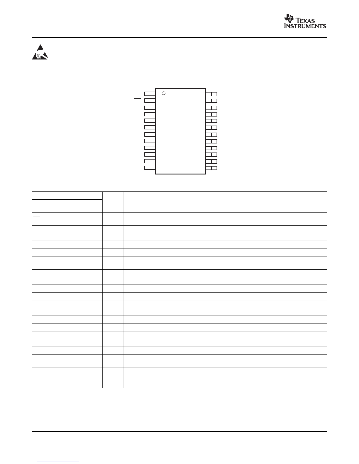
1
2
3
4
5
6
7
8
9
10
11
12
24
23
22
21
20
19
18
17
16
15
14
13
PVCCL
SD
PVCCL
MUTE
LIN
RIN
BYPASS
AGND
AGND
PVCCR
VCLAMP
PVCCR
PGNDL
PGNDL
LOUT
BSL
AVCC
AVCC
GAIN0
GAIN1
BSR
ROUT
PGNDR
PGNDR
TPA3120D2
SLOS507E – MARCH 2007 – REVISED SEPTEMBER 2007
These devices have limited built-in ESD protection. The leads should be shorted together or the device placed in conductive foam
during storage or handling to prevent electrostatic damage to the MOS gates.
TERMINAL
NAME
SD 2 I
RIN 6 I Audio input for right channel
LIN 5 I Audio input for left channel
GAIN0 18 I Gain select least-significant bit. TTL logic levels with compliance to AVCC
GAIN1 17 I Gain select most-significant bit. TTL logic levels with compliance to AVCC
MUTE 4 I
BSL 21 I/O Bootstrap I/O for left channel
PVCCL 1, 3 P Power supply for left-channel H-bridge, not internally connected to PVCCR or AVCC
LOUT 22 O Class-D 1/2-H-bridge positive output for left channel
PGNDL 23, 24 P Power ground for left-channel H-bridge
VCLAMP 11 P Internally generated voltage supply for bootstrap capacitors
BSR 16 I/O Bootstrap I/O for right channel
ROUT 15 O Class-D 1/2-H-bridge negative output for right channel
PGNDR 13, 14 P Power ground for right-channel H-bridge.
PVCCR 10, 12 P Power supply for right-channel H-bridge, not connected to PVCCL or AVCC
AGND 9 P Analog ground for digital/analog cells in core
AGND 8 P Analog ground for analog cells in core
BYPASS 7 O
AVCC 19, 20 P High-voltage analog power supply. Not internally connected to PVCCR or PVCCL
Thermal pad Die pad P
2 Submit Documentation Feedback Copyright © 2007, Texas Instruments Incorporated
24-PIN
(PWP)
I/O/P DESCRIPTION
PWP (TSSOP) PACKAGE
(TOP VIEW)
Table 1. TERMINAL FUNCTIONS
Shutdown signal for IC (low = disabled, high = operational). TTL logic levels with compliance to
AVCC
Mute signal for quick disable/enable of outputs (high = outputs switch at 50% duty cycle, low =
outputs enabled). TTL logic levels with compliance to AVCC
Reference for preamplifier inputs. Nominally equal to AVCC/8. Also controls start-up time via
external capacitor sizing.
Connect to ground. Thermal pad should be soldered down on all applications to secure the
device properly to the printed wiring board.
Product Folder Link(s): TPA3120D2
Page 3

www.ti.com
TPA3120D2
SLOS507E – MARCH 2007 – REVISED SEPTEMBER 2007
ABSOLUTE MAXIMUM RATINGS
over operating free-air temperature range (unless otherwise noted)
V
CC
V
I
V
IN
T
A
T
J
T
stg
R
L
ESD Electrostatic Discharge
(1) Stresses beyond those listed under absolute maximum ratings may cause permanent damage to the device. These are stress ratings
only, and functional operations of the device at these or any other conditions beyond those indicated under recommended operating
conditions is not implied. Exposure to absolute-maximum-rated conditions for extended periods may affect device reliability.
Supply voltage AVCC, PVCC – 0.3 to 36 V
Logic input voltage SD, MUTE, GAIN0, GAIN1 – 0.3 to V
Analog input voltage RIN, LIN – 0.3 to 7 V
Continuous total power dissipation See Dissipation Ratings table
Operating free-air temperature range – 40 to 85 ° C
Operating junction temperature range – 40 to 150 ° C
Storage temperature range – 65 to 150 ° C
Load resistance (minimum value) 3.2 Ω
Human-body model (all pins) ± 2 kV
Charged-device model (all
pins)
(1)
VALUE UNIT
+ 0.3 V
CC
± 500 V
DISSIPATION RATINGS
PACKAGE
24-pin TSSOP 4.16 W 33.3 mW/ ° C 2.67 W 2.16 W
(1) For the most current package and ordering information, see the Package Option Addendum at the end of this document, or see the TI
website at www.ti.com .
(2) This data was taken using 1 oz trace and copper pad that is soldered directly to a JEDEC standard high-k PCB. The thermal pad must
be soldered to a thermal land on the printed-circuit board. See the PowerPAD Thermally Enhanced Package application note
(SLMA002 ).
(1) (2)
TA≤ 25 ° C DERATING FACTOR TA= 70 ° C TA= 85 ° C
RECOMMENDED OPERATING CONDITIONS
V
CC
V
IH
V
IL
I
IH
I
IL
T
A
Supply voltage PVCC, AVCC 10 30 V
High-level input voltage SD, MUTE, GAIN0, GAIN1 2 V
Low-level input voltage SD, MUTE, GAIN0, GAIN1 0.8 V
High-level input current MUTE, VI= VCC, V
Low-level input current MUTE, VI= 0 V, V
Operating free-air temperature – 40 85 ° C
SD, VI= VCC, V
= 30 V 125
CC
= 30 V 125 μ A
CC
GAIN0, GAIN1, VI= VCC, V
SD, VI= 0, V
= 30 V 1
CC
= 30 V 1 μ A
CC
GAIN0, GAIN1, VI= 0 V, V
MIN MAX UNIT
= 24 V 125
CC
= 24 V 1
CC
Copyright © 2007, Texas Instruments Incorporated Submit Documentation Feedback 3
Product Folder Link(s): TPA3120D2
Page 4
www.ti.com
TPA3120D2
SLOS507E – MARCH 2007 – REVISED SEPTEMBER 2007
DC CHARACTERISTICS
TA= 25 ° C, V
| V
| (measured differentially in BTL VI= 0 V, AV= 36 dB 7.5 50 mV
OS
V
(BYPASS)
I
CC(q)
I
CC(q)
I
CC(q)
r
DS(on)
G Gain dB
= 24 V, RL= 4 Ω (unless otherwise noted)
CC
PARAMETER TEST CONDITIONS MIN TYP MAX UNIT
Class-D output offset voltage
mode as shown in Fig 30)
Bypass output voltage No load AVCC/8 V
Quiescent supply current SD = 2 V, MUTE = 0 V, No load 23 37 mA
Quiescent supply current in
mute mode
Quiescent supply current in
shutdown mode
Drain-source on-state
resistance
MUTE = 0.8 V, No load 23 mA
SD = 0.8 V , No load 0.39 1 mA
200 m Ω
GAIN1 = 0.8 V
GAIN = 2 V
GAIN0 = 0.8 V 18 20 22
GAIN0 = 2 V 24 26 28
GAIN0 = 0.8 V 30 32 34
GAIN0 = 2 V 34 36 38
Mute Attenuation VI= 1Vrms – 82 dB
AC CHARACTERISTICS
TA= 25 ° C, V
ksvr Supply ripple rejection dB
P
O
THD+N
V
n
SNR Signal-to-noise ratio 99 dB
f
OSC
= 24 V, RL= 4 Ω (unless otherwise noted)
CC
PARAMETER TEST CONDITIONS MIN TYP MAX UNIT
V
Output power at 1% THD+N
Output power at 10% THD+N
Total harmonic distortion +
noise
Output integrated noise floor
= 24, V
CC
Gain = 20 dB
V
= 24 V, RL= 4 Ω , f = 1 kHz 16
CC
V
= 24 V, RL= 8 Ω , f = 1 kHz 8
CC
VCC= 24 V, RL= 4 Ω , f = 1 kHz 20
V
= 24 V, RL= 8 Ω , f = 1 kHz 10
CC
RL= 4 Ω , f = 1 kHz, PO= 10 W 0.08%
RL= 8 Ω , f = 1 kHz, PO= 5 W 0.08%
20 Hz to 22 kHz, A-weighted filter,
Gain = 20 dB
= 200 mV
ripple
100 Hz – 48
PP
1 kHz – 52
85 μ V
– 80 dBV
Crosstalk PO= 1 W, f = 1 kHz; Gain = 20 dB – 60 dB
Max output at THD+N < 1%, f = 1 kHz,
Gain = 20 dB
Thermal trip point 150 ° C
Thermal hysteresis 30 ° C
Oscillator frequency 230 250 270 kHz
W
4 Submit Documentation Feedback Copyright © 2007, Texas Instruments Incorporated
Product Folder Link(s): TPA3120D2
Page 5
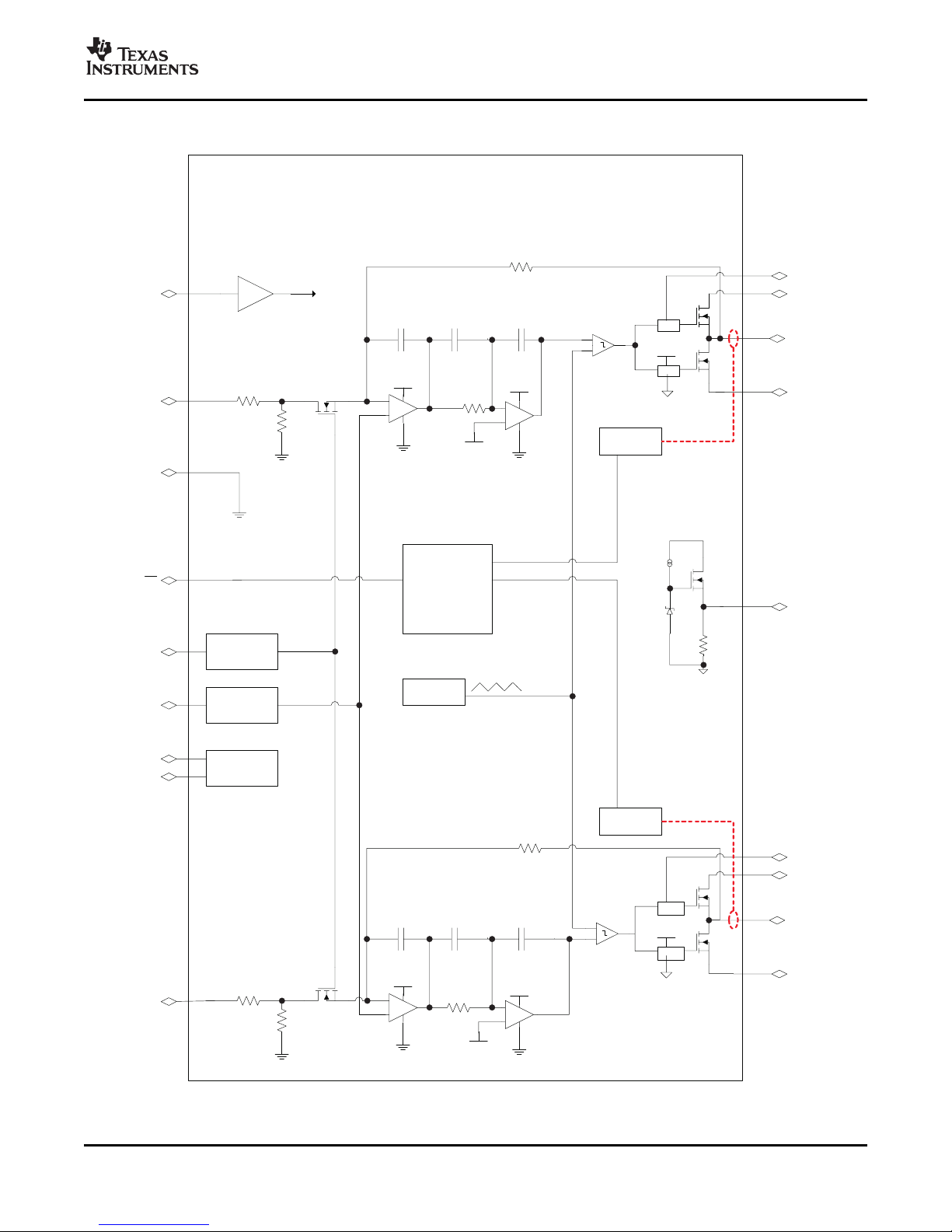
www.ti.com
LS
HS
LS
HS
OSC/RAMP
MUTE
CONTROL
BYPASS
AV
CONTROL
CONTROL
BIAS
THERMAL
SC
DETECT
SC
DETECT
AVDD
AVCC
LIN
RIN
MUTE
BYPASS
GAIN1
GAIN0
SD
BSL
PVCCL
LOUT
PGNDL
VCLAMP
BSR
PVCCR
ROUT
PGNDR
VCLAMP
VCLAMP
AVDD
AVDD
AVDD/2
AVDD
AVDD
AVDD/2
REGULATOR
FUNCTIONAL BLOCK DIAGRAM
AGND
+
-
+
-
FUNCTIONAL BLOCK DIAGRAM
TPA3120D2
SLOS507E – MARCH 2007 – REVISED SEPTEMBER 2007
Copyright © 2007, Texas Instruments Incorporated Submit Documentation Feedback 5
Product Folder Link(s): TPA3120D2
Page 6
www.ti.com
f − Frequency − Hz
20 100
1k
10k
THD+N
T
otalHarmonicDistortion+Noise
%
-
-
0.1
10
20k
1
0.01
V =18V
R =4 (SE)
Gain=20dB
CC
L
W
P =5W
O
P =2.5W
O
P =1W
O
f − Frequency − Hz
20 100 1k 10k
THD+N
T
otalHarmonicDistortion+Noise
%
-
-
0.1
10
20k
1
0.01
V =24V
R =4 (SE)
Gain=20dB
CC
L
W
P =10W
O
P =1W
O
P =5W
O
f − Frequency − Hz
20 100 1k 10k
THD+N
T
otalHarmonicDistortion+Noise
%
-
-
0.1
10
20k
1
0.01
V =24V
R =8 (SE)
Gain=20dB
CC
L
W
P =1W
O
P =2.5W
O
P =5W
O
P − OutputPower − W
O
10m 100m 1 10
THD+N
T
otalHarmonicDistortion+Noise
%
-
-
1
40
10
0.01
0.1
V =12V
CC
V =24V
CC
V =18V
CC
R =4 (SE)
Gain=20dB
L
W
TPA3120D2
SLOS507E – MARCH 2007 – REVISED SEPTEMBER 2007
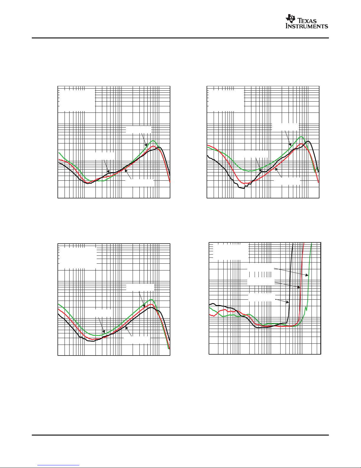
All tests are made at frequency = 1 kHz unless otherwise noted.
TYPICAL CHARACTERISTICS
TOTAL HARMONIC DISTORTION + NOISE TOTAL HARMONIC DISTORTION + NOISE
vs vs
FREQUENCY FREQUENCY
Figure 1. Figure 2.
TOTAL HARMONIC DISTORTION + NOISE TOTAL HARMONIC DISTORTION + NOISE
vs vs
FREQUENCY OUTPUT POWER
6 Submit Documentation Feedback Copyright © 2007, Texas Instruments Incorporated
Figure 3. Figure 4.
Product Folder Link(s): TPA3120D2
Page 7
www.ti.com
THD+N-TotalHarmonicDistortion+Noise-%
P − OutputPower − W
O
R =8 (SE)
Gain=20dB
L
W
1
10
0.01
0.1
10m 100m 1 10 40
V =12V
CC
V =24V
CC
V =18V
CC
-100
20 100
1k
20k
f − Frequency − Hz
Crosstalk
dB
-
10k
-90
-80
-70
-60
-50
-40
-30
-20
-10
0
RtoL
L toR
V =18V
V =1Vrms
R =4 (SE)
Gain=20dB
CC
O
L
W
-300
200
-200
-100
0
100
0
20
5
10
15
20 100k100 200 1k 2k 10k 20k
f − Frequency − Hz
Gain dB
-
Phase
-
o
Gain
Phase
V =24V
R =4 (SE)
Gain=20dB
L =33 H
C =1 F
C =470 F
CC
L
filt
filt
dc
W
m
m
m
-100
20 100
1k
20k
f − Frequency − Hz
10k
-90
-80
-70
-60
-50
-40
-30
-20
-10
0
Crosstalk
dB
-
L toR
RtoL
V =18V,
V =1V,
R =8 ,
Gain=20dB
CC
O
L
W
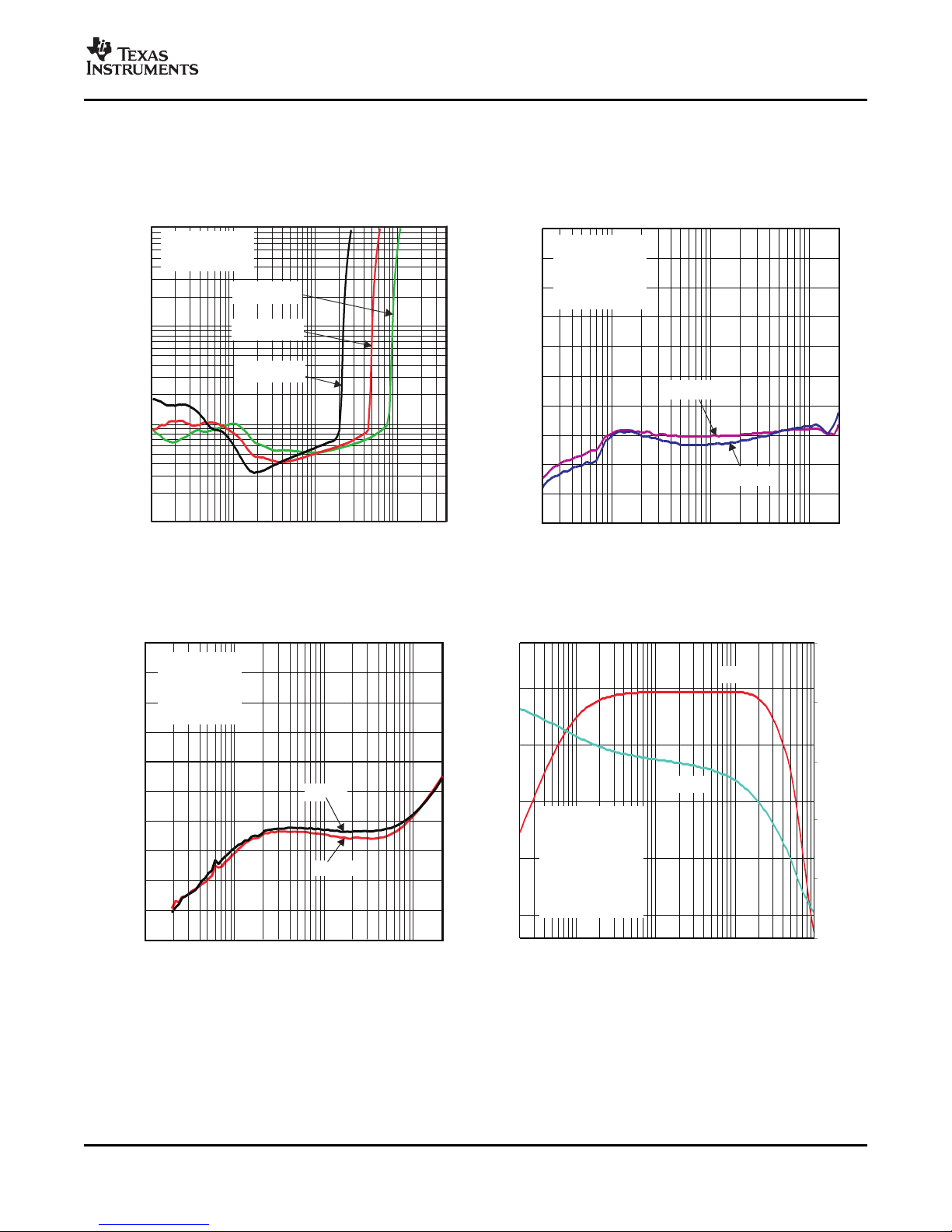
TYPICAL CHARACTERISTICS (continued)
All tests are made at frequency = 1 kHz unless otherwise noted.
TPA3120D2
SLOS507E – MARCH 2007 – REVISED SEPTEMBER 2007
TOTAL HARMONIC DISTORTION + NOISE CROSSTALK
vs vs
OUTPUT POWER FREQUENCY
Figure 5. Figure 6.
CROSSTALK GAIN/PHASE
vs vs
FREQUENCY FREQUENCY
Copyright © 2007, Texas Instruments Incorporated Submit Documentation Feedback 7
Figure 7. Figure 8.
Product Folder Link(s): TPA3120D2
Page 8
www.ti.com
-250
200
-200
-150
-100
-50
0
50
100
150
5
22.5
7.5
10
12.5
15
17.5
20
20 100k100 200 1k 2k 10k 20k
f − Frequency − Hz
Gain dB
-
Phase
-
o
Gain
Phase
V =24V
R =8 (SE)
Gain=20dB
L =47 H
C =0.22 F
C =470 F
CC
L
filt
filt
dc
W
m
m
m
V − SupplyVoltage − V
SS
16 26
P
OutputPower
W
O
-
-
22
30
28
4
32
12
THD=10%
THD=1%
R =4 (SE)
Gain=20dB
L
W
6
8
2
14
18
10
16
20
24
30
26
1210 14 18 20 22 24 28
THD=10%
THD=1%
V -SupplyVoltage-V
SS
P -OutputPower-W
O
R =8 (SE)
Gain=20dB
L
W
16 26 301210
7
14 18 20 22 24 28
17
16
15
14
13
12
11
10
9
6
1
8
5
4
3
2
P − OutputPower − W
O
6 16
Efficiency
%
-
80
20
10
100
30
12V
18V
24V
R =4 (SE)
Gain=20dB
L
W
0
40
60
20
50
70
90
20 4 8 10 12 14 18
TPA3120D2
SLOS507E – MARCH 2007 – REVISED SEPTEMBER 2007
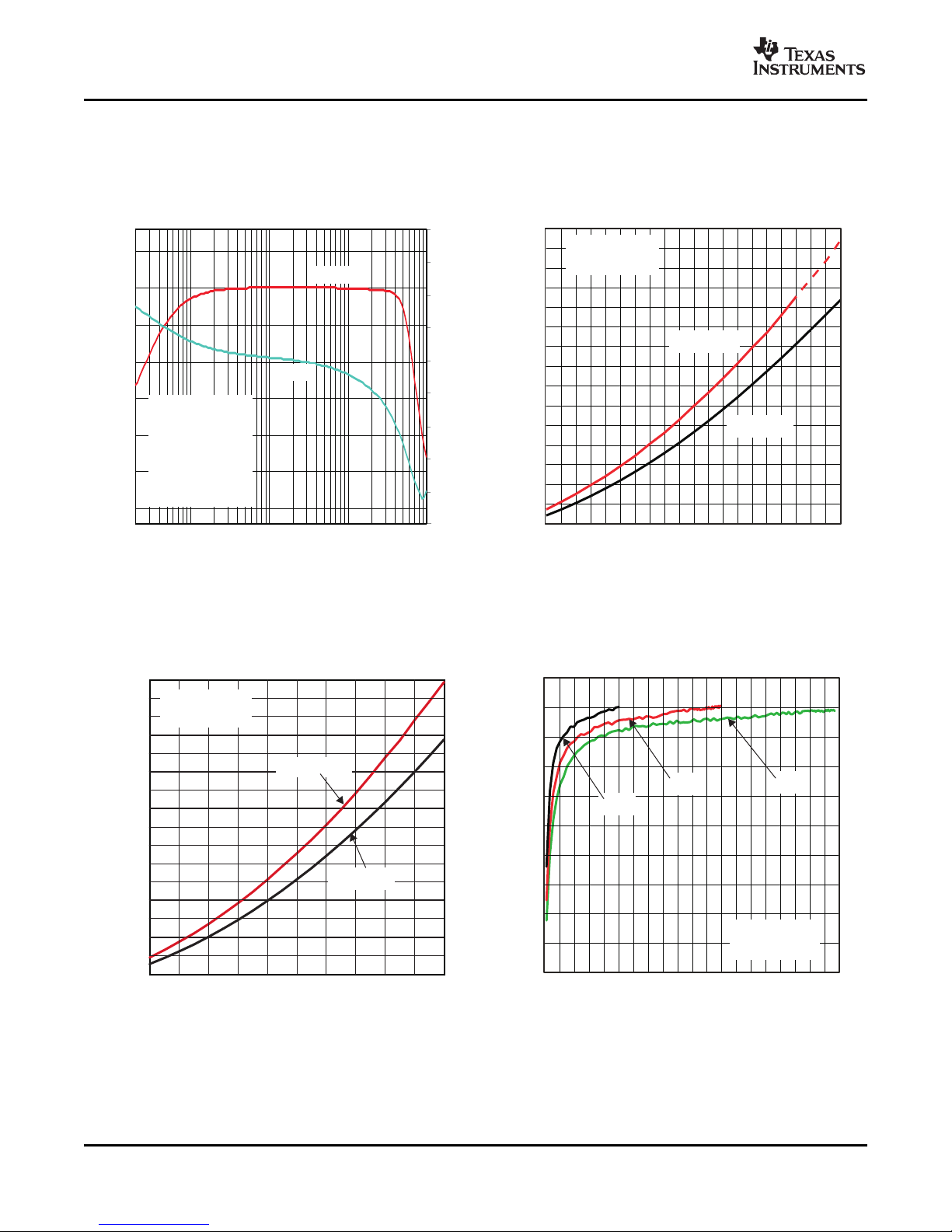
TYPICAL CHARACTERISTICS (continued)
All tests are made at frequency = 1 kHz unless otherwise noted.
GAIN/PHASE OUTPUT POWER
vs vs
FREQUENCY SUPPLY VOLTAGE
Figure 9.
OUTPUT POWER EFFICIENCY
vs vs
SUPPLY VOLTAGE OUTPUT POWER
8 Submit Documentation Feedback Copyright © 2007, Texas Instruments Incorporated
Figure 11. Figure 12.
Product Folder Link(s): TPA3120D2
A. Dashed line represents thermally limited
region.
Figure 10.
Page 9
www.ti.com
P − OutputPower − W
O
Efficiency
%
-
80
10
100
30
0
40
60
20
50
70
90
12
0 1 2 3 4 5 6 7 8 9
10 11
R =8 (SE)
Gain=20dB
L
W
12V
18V
24V
P − OutputPower − W
O
I
−
SupplyCurrent
−
A
C
C
12 32
1.6
40
0.2
2
0.6
18V
0
0.8
1.2
0.4
1
1.4
1.8
40 8 16 20 24 28 36
R =4 (SE)
Gain=20dB
L
W
24V
12V
-120
20 100
1k
20k
f − Frequency − Hz
PowerSupplyRejectionRatio
dB
-
10k
-110
-100
-90
-80
-70
-50
0
V =24V
V =0.2V
R =4 (SE)
Gain=20dB
CC
O(ripple) PP
L
W
-40
-30
-20
-10
-60
0.9
0.8
0.7
0.6
0.5
0.4
0.3
0.2
0.1
0
0 2.5 5 7.5 10 12.5 15 17.5 20 22.5 25
P -OutputPower-W
O
I -SupplyCurrent- A
CC
12V
18V
24V
R =8 ,
Gain=20dB
L
W
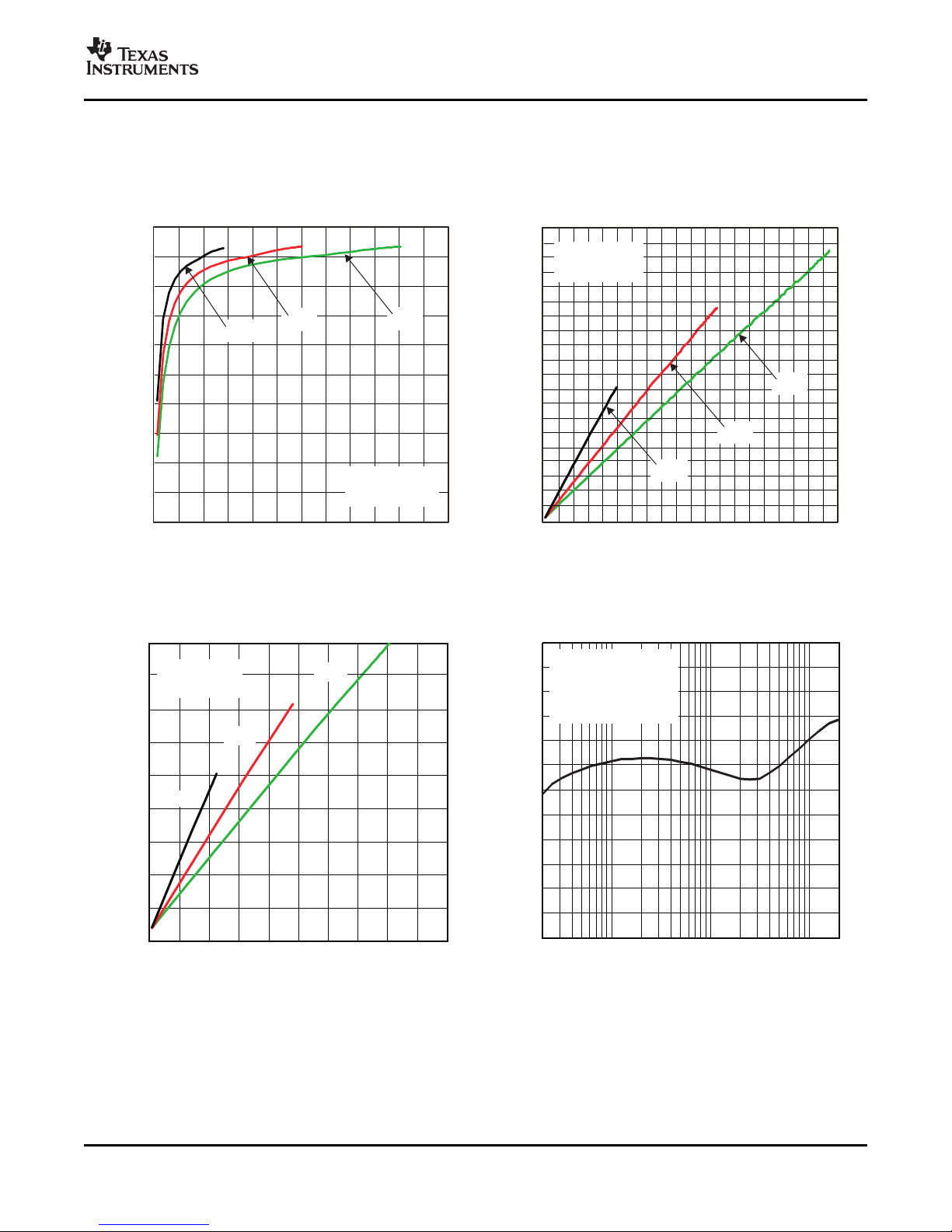
TYPICAL CHARACTERISTICS (continued)
All tests are made at frequency = 1 kHz unless otherwise noted.
EFFICIENCY SUPPLY CURRENT
vs vs
OUTPUT POWER OUTPUT POWER
TPA3120D2
SLOS507E – MARCH 2007 – REVISED SEPTEMBER 2007
Figure 13. Figure 14.
SUPPLY CURRENT POWER SUPPLY REJECTION RATIO
vs vs
OUTPUT POWER FREQUENCY
Copyright © 2007, Texas Instruments Incorporated Submit Documentation Feedback 9
Figure 15. Figure 16.
Product Folder Link(s): TPA3120D2
Page 10

www.ti.com
f − Frequency − Hz
20 100 1k 10k
THD+N
T
otalHarmonicDistortion+Noise
%
-
-
0.1
10
20k
1
0.01
0.001
V =24V
R =8 (BTL)
Gain=20dB
CC
L
W
P =20W
O
P =1W
O
P =5W
O
R =8 (BTL)
Gain=20dB
L
W
P − OutputPower − W
O
10m 100m 1 10
THD+N
T
otalHarmonicDistortion+Noise
%
-
-
1
40
10
0.01
0.1
V =12V
CC
V =24V
CC
V =18V
CC
-200
400
-100
0
100
200
300
-30
30
-20
-10
0
10
20
20 200k100 1k 10k
f-Frequency-Hz
Phase-°
Gain-dB
Phase
Gain
V =24V,
R =8 (BTL),
Gain=20dB,
L =33 H,
C =1 F
CC
L
filt
filt
W
m
m
V − SupplyVoltage − V
SS
16 26
P
OutputPower
W
O
-
-
40
30
55
0
65
15
THD=10%
THD=1%
R =8 (BTL)
Gain=20dB
L
W
20
30
10
25
35
45
60
50
1210 14 18 20 22 24 28
5
TPA3120D2
SLOS507E – MARCH 2007 – REVISED SEPTEMBER 2007
TYPICAL CHARACTERISTICS (continued)
All tests are made at frequency = 1 kHz unless otherwise noted.
TOTAL HARMONIC DISTORTION + NOISE TOTAL HARMONIC DISTORTION + NOISE
vs vs
FREQUENCY OUTPUT POWER
Figure 17. Figure 18.
GAIN/PHASE OUTPUT POWER
vs vs
FREQUENCY SUPPLY VOLTAGE
Figure 19.
10 Submit Documentation Feedback Copyright © 2007, Texas Instruments Incorporated
A. Dashed line represents thermally limited
region.
Figure 20.
Product Folder Link(s): TPA3120D2
Page 11

www.ti.com
P − OutputPower − W
O
32
Efficiency
%
-
80
40
10
100
30
R =8 (BTL)
Gain=20dB
L
W
0
40
60
20
50
70
90
40 8 16 20 24 28 36
12V
18V
24V
12
-140
20 100
1k
20k
f − Frequency − Hz
PowerSupplyRejectionRatio
dB
-
10k
-120
-100
-80
-60
-40
-20
0
V =24V
V =200mV
R =8 (BTL)
Gain=20dB
CC
O(ripple)
L
W
TYPICAL CHARACTERISTICS (continued)
All tests are made at frequency = 1 kHz unless otherwise noted.
EFFICIENCY POWER SUPPLY REJECTION RATIO
vs vs
OUTPUT POWER FREQUENCY
TPA3120D2
SLOS507E – MARCH 2007 – REVISED SEPTEMBER 2007
Figure 21. Figure 22.
Copyright © 2007, Texas Instruments Incorporated Submit Documentation Feedback 11
Product Folder Link(s): TPA3120D2
Page 12
www.ti.com
+V
CC
0V
OutputCurrent
OutputCurrent
+V
CC
0V
+V
CC
0V
+V
CC
0V
–V
CC
DifferentialVoltage
AcrossSpeaker
TPA3120D2
SLOS507E – MARCH 2007 – REVISED SEPTEMBER 2007
APPLICATION INFORMATION
CLASS-D OPERATION
This section focuses on the class-D operation of the TPA3120D2.
Traditional Class-D Modulation Scheme
The TPA3120D2 operates in AD mode. There are two main configurations that may be used. For stereo
operation, the TPA3120D2 should be configured in a single-ended (SE) half-bridge amplifier. For mono
applications, TPA3120D2 may be used as a bridge-tied-load (BTL) amplifier. The traditional class-D modulation
scheme, which is used in the TPA3120D2 BTL configuration, has a differential output where each output is 180
degrees out of phase and changes from ground to the supply voltage, V
output varies between positive and negative V
, where filtered 50% duty cycle yields
CC
0 V across the load. The class-D modulation scheme with voltage and current waveforms is shown in Figure 23
and Figure 24 .
. Therefore, the differential prefiltered
CC
Figure 23. Class-D Modulation for TPA3120D2 SE Configuration
Figure 24. Class-D Modulation for TPA3120D2 BTL Configuration
Supply Pumping
One issue encountered in single-ended (SE) class-D amplifier designs is supply pumping. Power-supply pumping
is a rise in the local supply voltage due to energy being driven back to the supply by operation of the class-D
amplifier. This phenomenon is most evident at low audio frequencies and when both channels are operating at
the same frequency and phase. At low levels, power-supply pumping results in distortion in the audio output due
to fluctuations in supply voltage. At higher levels, pumping can cause the overvoltage protection to operate,
which temporarily shuts down the audio output.
12 Submit Documentation Feedback Copyright © 2007, Texas Instruments Incorporated
Product Folder Link(s): TPA3120D2
Page 13

www.ti.com
C
i
IN
Z
i
Z
f
Input
Signal
f=
1
2 Z Cp
i i
TPA3120D2
SLOS507E – MARCH 2007 – REVISED SEPTEMBER 2007
Several things can be done to relieve power-supply pumping. The lowest impact is to operate the two inputs out
of phase 180 ° and reverse the speaker connections. Because most audio is highly correlated, this causes the
supply pumping to be out of phase and not as severe. If this is not enough, the amount of bulk capacitance on
the supply must be increased. Also, improvement is realized by hooking other supplies to this node, thereby,
sinking some of the excess current. Power-supply pumping should be tested by operating the amplifier at low
frequencies and high output levels.
Gain Setting via GAIN0 and GAIN1 Inputs
The gain of the TPA3120D2 is set by two input terminals, GAIN0 and GAIN1.
The gains listed in Table 2 are realized by changing the taps on the input resistors and feedback resistors inside
the amplifier. This causes the input impedance (Z
are controlled by ratios of resistors, so the gain variation from part-to-part is small. However, the input impedance
from part-to-part at the same gain may shift by ± 20% due to shifts in the actual resistance of the input resistors.
For design purposes, the input network (discussed in the next section) should be designed assuming an input
impedance of 8 k Ω , which is the absolute minimum input impedance of the TPA3120D2. At the higher gain
settings, the input impedance could increase as high as 72 k Ω .
GAIN1 GAIN0 (k Ω ),
0 0 20 60
0 1 26 30
1 0 32 15
1 1 36 9
) to be dependent on the gain setting. The actual gain settings
i
Table 2. Gain Setting
AMPLIFIER GAIN (dB),
TYPICAL
INPUT IMPEDANCE
TYPICAL
INPUT RESISTANCE
Changing the gain setting can vary the input resistance of the amplifier from its smallest value, 10 k Ω ± 20%, to
the largest value, 60 k Ω ± 20%. As a result, if a single capacitor is used in the input high-pass filter, the – 3-dB
cutoff frequency may change when changing gain steps.
The – 3-dB frequency can be calculated using Equation 1 . Use the Zivalues given in Table 2 .
(1)
Copyright © 2007, Texas Instruments Incorporated Submit Documentation Feedback 13
Product Folder Link(s): TPA3120D2
Page 14
www.ti.com
f =
c
1
2 Z Cp
i i
–3dB
f
c
C =
i
1
2 Z fp
i c
TPA3120D2
SLOS507E – MARCH 2007 – REVISED SEPTEMBER 2007
INPUT CAPACITOR, C
In the typical application, an input capacitor (C
proper dc level for optimum operation. In this case, C
i
) is required to allow the amplifier to bias the input signal to the
i
and the input impedance of the amplifier (Z
i
) form a
i
high-pass filter with the corner frequency determined in Equation 2 .
The value of Ciis important, as it directly affects the bass (low-frequency) performance of the circuit. Consider
the example where Ziis 20 k Ω and the specification calls for a flat bass response down to 20 Hz. Equation 2 is
reconfigured as Equation 3 .
In this example, Ciis 0.4 μ F; so, one would likely choose a value of 0.47 μ F as this value is commonly used. If
the gain is known and is constant, use Zifrom Table 2 to calculate Ci. A further consideration for this capacitor is
the leakage path from the input source through the input network (C
) and the feedback network to the load. This
i
leakage current creates a dc offset voltage at the input to the amplifier that reduces useful headroom, especially
in high-gain applications. For this reason, a low-leakage tantalum or ceramic capacitor is the best choice. When
polarized capacitors are used, the positive side of the capacitor should face the amplifier input in most
applications as the dc level there is held at 2 V, which is likely higher than the source dc level. Note that it is
important to confirm the capacitor polarity in the application. Additionally, lead-free solder can create dc offset
voltages, and it is important to ensure that boards are cleaned properly.
(2)
(3)
Single-Ended Output Capacitor, C
In single-ended (SE) applications, the dc blocking capacitor forms a high-pass filter with the speaker impedance.
The frequency response rolls of with decreasing frequency at a rate of 20 dB/decade. The cutoff frequency is
determined by
fc= 1/2 π COZ
Table 3 shows some common component values and the associated cutoff frequencies:
Speaker Impedance ( Ω )
14 Submit Documentation Feedback Copyright © 2007, Texas Instruments Incorporated
L
4 680 1000 2200
8 330 470 1000
O
Table 3. Common Filter Responses
C
– DC Blocking Capacitor ( μ F)
SE
fc= 60 Hz ( – 3 dB) fc= 40 Hz ( – 3 dB) fc= 20 Hz ( – 3 dB)
Product Folder Link(s): TPA3120D2
Page 15

www.ti.com
LOUT /ROUT
L
filter
C
filter
LOUT
L
filter
C
filter
L
filter
C
filter
ROUT
TPA3120D2
SLOS507E – MARCH 2007 – REVISED SEPTEMBER 2007
Output Filter and Frequency Response
For the best frequency response, a flat-passband output filter (second-order Butterworth) may be used. The
output filter components consist of the series inductor and capacitor to ground at the LOUT and ROUT pins.
There are several possible configurations, depending on the speaker impedance and whether the output
configuration is single-ended (SE) or bridge-tied load (BTL). Table 4 lists the recommended values for the filter
components. It is important to use a high-quality capacitor in this application. A rating of at least X7R is required.
Table 4. Recommended Filter Output Components
Output Configuration Speaker Impedance ( Ω ) Filter Inductor ( μ H) Filter Capacitor (nF)
Single Ended (SE)
Bridge Tied Load (BTL)
4 22 680
8 47 390
4 10 1500
8 22 680
Figure 25. BTL Filter Configuration Figure 26. SE Filter Configuration
Power-Supply Decoupling, C
S
The TPA3120D2 is a high-performance CMOS audio amplifier that requires adequate power-supply decoupling
to ensure that the output total harmonic distortion (THD) is as low as possible. Power-supply decoupling also
prevents oscillations for long lead lengths between the amplifier and the speaker. The optimum decoupling is
achieved by using two capacitors of different types that target different types of noise on the power-supply leads.
For higher-frequency transients, spikes, or digital hash on the line, a good low equivalent-series-resistance (ESR)
ceramic capacitor, typically 0.1 μ F to 1 μ F, placed as close as possible to the device V
lead works best. For
CC
filtering lower frequency noise signals, a larger aluminum electrolytic capacitor of 470 μ F or greater placed near
the audio power amplifier is recommended. The 470- μ F capacitor also serves as local storage capacitor for
supplying current during large signal transients on the amplifier outputs. The PVCC terminals provide the power
to the output transistors, so a 470- μ F or larger capacitor should be placed on each PVCC terminal. A 10- μ F
capacitor on the AVCC terminal is adequate. These capacitors must be properly derated for voltage and
ripple-current rating to ensure reliability.
BSN and BSP Capacitors
The half H-bridge output stages use only NMOS transistors. Therefore, they require bootstrap capacitors for the
high side of each output to turn on correctly. A 220-nF ceramic capacitor, rated for at least 25 V, must be
connected from each output to its corresponding bootstrap input. Specifically, one 220-nF capacitor must be
connected from LOUT to BSL, and one 220-nF capacitor must be connected from ROUT to BSR.
The bootstrap capacitors connected between the BSx pins and their corresponding outputs function as a floating
power supply for the high-side N-channel power MOSFET gate-drive circuitry. During each high-side switching
cycle, the bootstrap capacitors hold the gate-to-source voltage high enough to keep the high-side MOSFETs
turned on.
Copyright © 2007, Texas Instruments Incorporated Submit Documentation Feedback 15
Product Folder Link(s): TPA3120D2
Page 16

www.ti.com
TPA3120D2
SLOS507E – MARCH 2007 – REVISED SEPTEMBER 2007
VCLAMP Capacitor
To ensure that the maximum gate-to-source voltage for the NMOS output transistors is not exceeded, one
internal regulator clamps the gate voltage. One 1- μ F capacitor must be connected from VCLAMP (pin 11) to
ground and must be rated for at least 16 V. The voltages at the VCLAMP terminal may vary with V
not be used for powering any other circuitry.
VBYP Capacitor Selection
The scaled supply reference (VBYP) nominally provides an AVCC/8 internal bias for the preamplifier stages. The
external capacitor for this reference (C
start-up or recovery from shutdown mode, C
) is a critical component and serves several important functions. During
BYP
determines the rate at which the amplifier starts. The start up
BYP
time is proportional to 0.5 s per microfarad. Thus, the recommended 1- μ F capacitor results in a start-up time of
approximately 500 ms. The second function is to reduce noise produced by the power supply caused by coupling
with the output drive signal. This noise could result in degraded power-supply rejection and THD+N.
The circuit is designed for a C
value of 1 μ F for best pop performance. The input capacitors should have the
BYP
same value. A ceramic or tantalum low-ESR capacitor is recommended.
SHUTDOWN OPERATION
The TPA3120D2 employs a shutdown mode of operation designed to reduce supply current (I
minimum level during periods of nonuse for power conservation. The SHUTDOWN input terminal should be held
high (see specification table for trip point) during normal operation when the amplifier is in use. Pulling
SHUTDOWN low causes the outputs to mute and the amplifier to enter a low-current state. Never leave
SHUTDOWN unconnected, because amplifier operation would be unpredictable.
For the best power-up pop performance, place the amplifier in the shutdown or mute mode prior to applying the
power-supply voltage.
) to the absolute
CC
and may
CC
MUTE Operation
The MUTE pin is an input for controlling the output state of the TPA3120D2. A logic high on this terminal causes
the outputs to run at a constant 50% duty cycle. A logic low on this pin enables the outputs. This terminal may be
used as a quick disable/enable of outputs when changing channels on a television or transitioning between
different audio sources.
The MUTE terminal should never be left floating. For power conservation, the SHUTDOWN terminal should be
used to reduce the quiescent current to the absolute minimum level.
USING LOW-ESR CAPACITORS
Low-ESR capacitors are recommended throughout this application section. A real (as opposed to ideal) capacitor
can be modeled simply as a resistor in series with an ideal capacitor. The voltage drop across this resistor
minimizes the beneficial effects of the capacitor in the circuit. The lower the equivalent value of this resistance,
the more the real capacitor behaves like an ideal capacitor.
SHORT-CIRCUIT PROTECTION
The TPA3120D2 has short-circuit protection circuitry on the outputs that prevents damage to the device during
output-to-output shorts and output-to-GND shorts after the filter and output capacitor (at the speaker terminal.)
Directly at the device terminals, the protection circuitry prevents damage to device during output-to-output,
output-to-ground, and output-to-supply. When a short circuit is detected on the outputs, the part immediately
disables the output drive. This is an unlatched fault. Normal operation is restored when the fault is removed.
16 Submit Documentation Feedback Copyright © 2007, Texas Instruments Incorporated
Product Folder Link(s): TPA3120D2
Page 17

www.ti.com
TPA3120D2
SLOS507E – MARCH 2007 – REVISED SEPTEMBER 2007
THERMAL PROTECTION
Thermal protection on the TPA3120D2 prevents damage to the device when the internal die temperature
exceeds 150 ° C. There is a ± 15 ° C tolerance on this trip point from device to device. Once the die temperature
exceeds the thermal set point, the device enters into the shutdown state and the outputs are disabled. This is not
a latched fault. The thermal fault is cleared once the temperature of the die is reduced by 30 ° C. The device
begins normal operation at this point with no external system interaction.
PRINTED-CIRCUIT BOARD (PCB) LAYOUT
Because the TPA3120D2 is a class-D amplifier that switches at a high frequency, the layout of the printed-circuit
board (PCB) should be optimized according to the following guidelines for the best possible performance.
• Decoupling capacitors — The high-frequency 0.1- μ F decoupling capacitors should be placed as close to the
PVCC (pins 1, 3, 10, and 12) and AVCC (pins 19 and 20) terminals as possible. The VBYP (pin 7) capacitor
and VCLAMP (pin 11) capacitor should also be placed as close to the device as possible. Large (220- μ F or
greater) bulk power-supply decoupling capacitors should be placed near the TPA3120D2 on the PVCCL and
PVCCR terminals.
• Grounding — The AVCC (pins 19 and 20) decoupling capacitor and VBYP (pin 7) capacitor should each be
grounded to analog ground (AGND, pins 8 and 9). The PVCCx decoupling capacitors and VCLAMP
capacitors should each be grounded to power ground (PGND, pins 13, 14, 23, and 24). Analog ground and
power ground should be connected at the thermal pad, which should be used as a central ground connection
or star ground for the TPA3120D2.
• Output filter — The reconstruction filter (L1, L2, C9, and C16) should be placed as close to the output terminals
as possible for the best EMI performance. The capacitors should be grounded to power ground.
• Thermal pad — The thermal pad must be soldered to the PCB for proper thermal performance and optimal
reliability. The dimensions of the thermal pad and thermal land are described in the mechanical section at the
back of the data sheet. See TI Technical Briefs SLMA002 and SLOA120 for more information about using the
thermal pad. For recommended PCB footprints, see figures at the end of this data sheet.
For an example layout, see the TPA3120D2 Evaluation Module (TPA3120D2EVM) User Manual, (SLOU189 ).
Both the EVM user manual and the thermal pad application note are available on the TI Web site at
http://www.ti.com .
Copyright © 2007, Texas Instruments Incorporated Submit Documentation Feedback 17
Product Folder Link(s): TPA3120D2
Page 18

www.ti.com
VCC
VCC
LeftIn
Shutdown
Control
Mute
Control
RightIn
10 Fm
22 Hm
470 Fm
0.68 Fm
TPA3120TPA3120
PVCCL
1
SD
2
PVCCL
3
MUTE
4
LIN
5
RIN
6
BYPASS
7
AGND
8
AGND
9
PVCCR
10
VCLAMP
11
PVCCR
12
PGNDR
13
PGNDR
14
ROUT
15
BSR
16
GAIN1
17
GAIN0
18
AVCC
19
AVCC
20
BSL
21
LOUT
22
PGNDL
23
PGNDL
24
THERMAL
25
1.0 Fm
+LOUT
0.22 Fm
-ROUT
-LOUT
+ROUT
0.1 Fm
1.0 Fm
470
470
470
F
F
F
m
m
m
1.0 Fm
1.0 Fm
1.0 Fm
1.0 Fm
0.22 Fm
22 Hm
0.68 Fm
+In
-In
+OUT+OUT
-OUT-OUT
VCC
VCC
Shutdown
Control
Mute
Control
10 Fm
22 Hm
470 Fm
0.68 Fm
TPA3120TPA3120
PVCCL
1
SD
2
PVCCL
3
MUTE
4
LIN
5
RIN
6
BYPASS
7
AGND
8
AGND
9
PVCCR
10
VCLAMP
11
PVCCR
12
PGNDR
13
PGNDR
14
ROUT
15
BSR
16
GAIN1
17
GAIN0
18
AVCC
19
AVCC
20
BSL
21
LOUT
22
PGNDL
23
PGNDL
24
THERMAL
25
1.0 Fm
0.22 Fm
0.1 Fm
1.0 Fm
470 Fm
1.0 Fm
1.0 Fm
1.0 Fm
1.0 Fm
0.22 Fm
22 Hm
0.68 Fm
TPA3120D2
SLOS507E – MARCH 2007 – REVISED SEPTEMBER 2007
Figure 27. Schematic for Single-Ended (SE) Configuration
Figure 28. Schematic for Bridge-Tied (BTL) Configuration
18 Submit Documentation Feedback Copyright © 2007, Texas Instruments Incorporated
Product Folder Link(s): TPA3120D2
Page 19

www.ti.com
TPA3120D2
SLOS507E – MARCH 2007 – REVISED SEPTEMBER 2007
BASIC MEASUREMENT SYSTEM
This section focuses on methods that use the basic equipment listed below:
• Audio analyzer or spectrum analyzer
• Digital multimeter (DMM)
• Oscilloscope
• Twisted-pair wires
• Signal generator
• Power resistor(s)
• Linear regulated power supply
• Filter components
• EVM or other complete audio circuit
Figure 29 shows the block diagrams of basic measurement systems for class-AB and class-D amplifiers. A sine
wave is normally used as the input signal because it consists of the fundamental frequency only (no other
harmonics are present). An analyzer is then connected to the audio power amplifier (APA) output to measure the
voltage output. The analyzer must be capable of measuring the entire audio bandwidth. A regulated dc power
supply is used to reduce the noise and distortion injected into the APA through the power pins. A System Two™
audio measurement system (AP-II) by Audio Precision™ includes the signal generator and analyzer in one
package.
The generator output and amplifier input must be ac-coupled. However, the EVMs already have the ac-coupling
capacitors, (C
attenuating the test signal, and is important because the input resistance of APAs is not high. Conversely, the
analyzer input impedance should be high. The output resistance, R
milliohms and can be ignored for all but the power-related calculations.
Figure 29 (a) shows a class-AB amplifier system. It takes an analog signal input and produces an analog signal
output. This amplifier circuit can be directly connected to the AP-II or other analyzer input.
This is not true of the class-D amplifier system shown in Figure 29 (b), which requires low-pass filters in most
cases in order to measure the audio output waveforms. This is because it takes an analog input signal and
converts it into a pulse-width modulated (PWM) output signal that is not accurately processed by some
analyzers.
), so no additional coupling is required. The generator output impedance should be low to avoid
IN
, of the APA is normally in the hundreds of
OUT
Copyright © 2007, Texas Instruments Incorporated Submit Documentation Feedback 19
Product Folder Link(s): TPA3120D2
Page 20

www.ti.com
Analyzer
20Hz-20kHz
(a)BasicClass-AB
APA
Signal
Generator
PowerSupply
Analyzer
20Hz-20kHz
R
L
(b)TraditionalClass-D
Class-D APA
Signal
Generator
PowerSupply
R
L
L
filt
C
filt
TPA3120D2
SLOS507E – MARCH 2007 – REVISED SEPTEMBER 2007
Figure 29. Audio Measurement Systems
20 Submit Documentation Feedback Copyright © 2007, Texas Instruments Incorporated
Product Folder Link(s): TPA3120D2
Page 21

www.ti.com
V
GEN
C
IN
C
L
R
IN
R
GEN
Twisted-PairWire
Generator
EvaluationModule
AudioPower
Amplifier
Twisted-PairWire
R
L
R
ANA
C
ANA
Analyzer
R
ANA
C
ANA
L
filt
C
filt
TPA3120D2
SLOS507E – MARCH 2007 – REVISED SEPTEMBER 2007
SE Input and SE Output (TPA3120D2 Stereo Configuration)
The SE input and output configuration is used with class-AB amplifiers. A block diagram of a fully SE
measurement circuit is shown in Figure 30 . SE inputs normally have one input pin per channel. In some cases,
two pins are present; one is the signal and the other is ground. SE outputs have one pin driving a load through
an output ac-coupling capacitor and the other end of the load is tied to ground. SE inputs and outputs are
considered to be unbalanced, meaning one end is tied to ground and the other to an amplifier input/output.
The generator should have unbalanced outputs, and the signal should be referenced to the generator ground for
best results. Unbalanced or balanced outputs can be used when floating, but they may create a ground loop that
affects the measurement accuracy. The analyzer should have balanced inputs to cancel out any common-mode
noise in the measurement.
Figure 30. SE Input — SE Output Measurement Circuit
The following general rules should be followed when connecting to APAs with SE inputs and outputs:
• Use an unbalanced source to supply the input signal.
• Use an analyzer with balanced inputs.
• Use twisted-pair wire for all connections.
• Use shielding when the system environment is noisy.
• Ensure the cables from the power supply to the APA, and from the APA to the load, can handle the large
currents (see Table 5 ).
Copyright © 2007, Texas Instruments Incorporated Submit Documentation Feedback 21
Product Folder Link(s): TPA3120D2
Page 22

www.ti.com
C
IN
AudioPower
Amplifier
Generator
C
IN
R
GEN
R
GEN
R
IN
R
IN
V
GEN
Analyzer
R
ANA
R
ANA
C
ANA
R
L
C
ANA
Twisted-PairWire
EvaluationModule
Twisted-PairWire
L
filt
L
filt
C
filt
C
filt
TPA3120D2
SLOS507E – MARCH 2007 – REVISED SEPTEMBER 2007
DIFFERENTIAL INPUT AND BTL OUTPUT (TPA3120D2 Mono Configuration)
Many of the class-D APAs and many class-AB APAs have differential inputs and bridge-tied-load (BTL) outputs.
Differential inputs have two input pins per channel and amplify the difference in voltage between the pins.
Differential inputs reduce the common-mode noise and distortion of the input circuit. BTL is a term commonly
used in audio to describe differential outputs. BTL outputs have two output pins providing voltages that are 180 °
out of phase. The load is connected between these pins. This has the added benefits of quadrupling the output
power to the load and eliminating a dc-blocking capacitor.
A block diagram of the measurement circuit is shown in Figure 31 . The differential input is a balanced input,
meaning the positive (+) and negative ( – ) pins have the same impedance to ground. Similarly, the SE output
equates to a balanced output.
Figure 31. Differential Input, BTL Output Measurement Circuit
The generator should have balanced outputs, and the signal should be balanced for best results. An unbalanced
output can be used, but it may create a ground loop that affects the measurement accuracy. The analyzer must
also have balanced inputs for the system to be fully balanced, thereby cancelling out any common-mode noise in
the circuit and providing the most accurate measurement.
The following general rules should be followed when connecting to APAs with differential inputs and BTL outputs:
• Use a balanced source to supply the input signal.
• Use an analyzer with balanced inputs.
• Use twisted-pair wire for all connections.
• Use shielding when the system environment is noisy.
• Ensure that the cables from the power supply to the APA, and from the APA to the load, can handle the large
currents (see Table 5 ).
Table 5 shows the recommended wire size for the power supply and load cables of the APA system. The real
concern is the dc or ac power loss that occurs as the current flows through the cable. These recommendations
are based on 12-inch (30.5-cm)-long wire with a 20-kHz sine-wave signal at 25 ° C.
Table 5. Recommended Minimum Wire Size for Power Cables
P
(W) RL( Ω ) AWG Size
OUT
10 4 18 22 16 40 18 42
2 4 18 22 3.2 8 3.7 8.5
1 8 22 28 2 8 2.1 8.1
< 0.75 8 22 28 1.5 6.1 1.6 6.2
22 Submit Documentation Feedback Copyright © 2007, Texas Instruments Incorporated
Product Folder Link(s): TPA3120D2
DC POWER LOSS AC POWER LOSS
(mW) (mW)
Page 23

PACKAGE OPTION ADDENDUM
www.ti.com 29-Apr-2009
PACKAGING INFORMATION
Orderable Device Status
(1)
Package
Type
Package
Drawing
Pins Package
Qty
Eco Plan
TPA3120D2PWP NRND HTSSOP PWP 24 60 Green (RoHS &
(2)
Lead/Ball Finish MSL Peak Temp
CU NIPDAU Level-3-260C-168 HR
(3)
no Sb/Br)
TPA3120D2PWPG4 NRND HTSSOP PWP 24 60 Green (RoHS &
CU NIPDAU Level-3-260C-168 HR
no Sb/Br)
TPA3120D2PWPR NRND HTSSOP PWP 24 2000 Green (RoHS &
CU NIPDAU Level-3-260C-168 HR
no Sb/Br)
TPA3120D2PWPRG4 NRND HTSSOP PWP 24 2000 Green (RoHS &
CU NIPDAU Level-3-260C-168 HR
no Sb/Br)
(1)
The marketing status values are defined as follows:
ACTIVE: Product device recommended for new designs.
LIFEBUY: TI has announced that the device will be discontinued, and a lifetime-buy period is in effect.
NRND: Not recommended for new designs. Device is in production to support existing customers, but TI does not recommend using this part in
a new design.
PREVIEW: Device has been announced but is not in production. Samples may or may not be available.
OBSOLETE: TI has discontinued the production of the device.
(2)
Eco Plan - The planned eco-friendly classification: Pb-Free (RoHS), Pb-Free (RoHS Exempt), or Green (RoHS & no Sb/Br) - please check
http://www.ti.com/productcontent for the latest availability information and additional product content details.
TBD: The Pb-Free/Green conversion plan has not been defined.
Pb-Free (RoHS): TI's terms "Lead-Free" or "Pb-Free" mean semiconductor products that are compatible with the current RoHS requirements
for all 6 substances, including the requirement that lead not exceed 0.1% by weight in homogeneous materials. Where designed to be soldered
at high temperatures, TI Pb-Free products are suitable for use in specified lead-free processes.
Pb-Free (RoHS Exempt): This component has a RoHS exemption for either 1) lead-based flip-chip solder bumps used between the die and
package, or 2) lead-based die adhesive used between the die and leadframe. The component is otherwise considered Pb-Free (RoHS
compatible) as defined above.
Green (RoHS & no Sb/Br): TI defines "Green" to mean Pb-Free (RoHS compatible), and free of Bromine (Br) and Antimony (Sb) based flame
retardants (Br or Sb do not exceed 0.1% by weight in homogeneous material)
(3)
MSL, Peak Temp. -- The Moisture Sensitivity Level rating according to the JEDEC industry standard classifications, and peak solder
temperature.
Important Information and Disclaimer:The information provided on this page represents TI's knowledge and belief as of the date that it is
provided. TI bases its knowledge and belief on information provided by third parties, and makes no representation or warranty as to the
accuracy of such information. Efforts are underway to better integrate information from third parties. TI has taken and continues to take
reasonable steps to provide representative and accurate information but may not have conducted destructive testing or chemical analysis on
incoming materials and chemicals. TI and TI suppliers consider certain information to be proprietary, and thus CAS numbers and other limited
information may not be available for release.
In no event shall TI's liability arising out of such information exceed the total purchase price of the TI part(s) at issue in this document sold by TI
to Customer on an annual basis.
Addendum-Page 1
Page 24

PACKAGE MATERIALS INFORMATION
www.ti.com 14-Jul-2012
TAPE AND REEL INFORMATION
*All dimensions are nominal
Device Package
TPA3120D2PWPR HTSSOP PWP 24 2000 330.0 16.4 6.95 8.3 1.6 8.0 16.0 Q1
Type
Package
Drawing
Pins SPQ Reel
Diameter
(mm)
Reel
Width
W1 (mm)
A0
(mm)B0(mm)K0(mm)P1(mm)W(mm)
Pin1
Quadrant
Pack Materials-Page 1
Page 25

PACKAGE MATERIALS INFORMATION
www.ti.com 14-Jul-2012
*All dimensions are nominal
Device Package Type Package Drawing Pins SPQ Length (mm) Width (mm) Height (mm)
TPA3120D2PWPR HTSSOP PWP 24 2000 367.0 367.0 38.0
Pack Materials-Page 2
Page 26

Page 27

Page 28
Page 29

IMPORTANT NOTICE
Texas Instruments Incorporated and its subsidiaries (TI) reserve the right to make corrections, enhancements, improvements and other
changes to its semiconductor products and services per JESD46C and to discontinue any product or service per JESD48B. Buyers should
obtain the latest relevant information before placing orders and should verify that such information is current and complete. All
semiconductor products (also referred to herein as “components”) are sold subject to TI’s terms and conditions of sale supplied at the time
of order acknowledgment.
TI warrants performance of its components to the specifications applicable at the time of sale, in accordance with the warranty in TI’s terms
and conditions of sale of semiconductor products. Testing and other quality control techniques are used to the extent TI deems necessary
to support this warranty. Except where mandated by applicable law, testing of all parameters of each component is not necessarily
performed.
TI assumes no liability for applications assistance or the design of Buyers’ products. Buyers are responsible for their products and
applications using TI components. To minimize the risks associated with Buyers’ products and applications, Buyers should provide
adequate design and operating safeguards.
TI does not warrant or represent that any license, either express or implied, is granted under any patent right, copyright, mask work right, or
other intellectual property right relating to any combination, machine, or process in which TI components or services are used. Information
published by TI regarding third-party products or services does not constitute a license to use such products or services or a warranty or
endorsement thereof. Use of such information may require a license from a third party under the patents or other intellectual property of the
third party, or a license from TI under the patents or other intellectual property of TI.
Reproduction of significant portions of TI information in TI data books or data sheets is permissible only if reproduction is without alteration
and is accompanied by all associated warranties, conditions, limitations, and notices. TI is not responsible or liable for such altered
documentation. Information of third parties may be subject to additional restrictions.
Resale of TI components or services with statements different from or beyond the parameters stated by TI for that component or service
voids all express and any implied warranties for the associated TI component or service and is an unfair and deceptive business practice.
TI is not responsible or liable for any such statements.
Buyer acknowledges and agrees that it is solely responsible for compliance with all legal, regulatory and safety-related requirements
concerning its products, and any use of TI components in its applications, notwithstanding any applications-related information or support
that may be provided by TI. Buyer represents and agrees that it has all the necessary expertise to create and implement safeguards which
anticipate dangerous consequences of failures, monitor failures and their consequences, lessen the likelihood of failures that might cause
harm and take appropriate remedial actions. Buyer will fully indemnify TI and its representatives against any damages arising out of the use
of any TI components in safety-critical applications.
In some cases, TI components may be promoted specifically to facilitate safety-related applications. With such components, TI’s goal is to
help enable customers to design and create their own end-product solutions that meet applicable functional safety standards and
requirements. Nonetheless, such components are subject to these terms.
No TI components are authorized for use in FDA Class III (or similar life-critical medical equipment) unless authorized officers of the parties
have executed a special agreement specifically governing such use.
Only those TI components which TI has specifically designated as military grade or “enhanced plastic” are designed and intended for use in
military/aerospace applications or environments. Buyer acknowledges and agrees that any military or aerospace use of TI components
which have not been so designated is solely at the Buyer's risk, and that Buyer is solely responsible for compliance with all legal and
regulatory requirements in connection with such use.
TI has specifically designated certain components which meet ISO/TS16949 requirements, mainly for automotive use. Components which
have not been so designated are neither designed nor intended for automotive use; and TI will not be responsible for any failure of such
components to meet such requirements.
Products Applications
Audio www.ti.com/audio Automotive and Transportation www.ti.com/automotive
Amplifiers amplifier.ti.com Communications and Telecom www.ti.com/communications
Data Converters dataconverter.ti.com Computers and Peripherals www.ti.com/computers
DLP® Products www.dlp.com Consumer Electronics www.ti.com/consumer-apps
DSP dsp.ti.com Energy and Lighting www.ti.com/energy
Clocks and Timers www.ti.com/clocks Industrial www.ti.com/industrial
Interface interface.ti.com Medical www.ti.com/medical
Logic logic.ti.com Security www.ti.com/security
Power Mgmt power.ti.com Space, Avionics and Defense www.ti.com/space-avionics-defense
Microcontrollers microcontroller.ti.com Video and Imaging www.ti.com/video
RFID www.ti-rfid.com
OMAP Mobile Processors www.ti.com/omap TI E2E Community e2e.ti.com
Wireless Connectivity www.ti.com/wirelessconnectivity
Mailing Address: Texas Instruments, Post Office Box 655303, Dallas, Texas 75265
Copyright © 2012, Texas Instruments Incorporated
 Loading...