

Page 1
INP
INN
SDSD
FaultFault
PLIMITPLIMIT
PVCC 8to26V
1uF
OUTN
FERRITE
BEAD
FILTER
OUTP
10W
8Ω
OUTN
FERRITE
BEAD
FILTER
FERRITE
BEAD
FILTER
OUTP
10W
8Ω
OUT+
-
OUT
Audio
Source
TPA3111D1
GAIN0
GAIN0
GAIN1GAIN1
TPA3111D1
www.ti.com
SLOS618E –AUGUST 2009–REVISED AUGUST 2012
10-W FILTER-FREE MONO CLASS-D AUDIO POWER AMPLIFIER with SPEAKER GUARD™
Check for Samples: TPA3111D1
1
FEATURES
2
• 10-W into an 8-Ω Load at 10% THD+N From a
12-V Supply
• 7-W into an 4-Ω Load at 10% THD+N From a 8V Supply
• 94% Efficient Class-D Operation into 8-Ω Load
Eliminates Need for Heat Sinks
• Wide Supply Voltage Range Allows Operation
from 8 to 26 V
• Filter-Free Operation
• SpeakerGuard™ Speaker Protection Includes
Adjustable Power Limiter plus DC Protection
• Flow Through Pin Out Facilitates Easy Board
Layout
• Robust Pin-to-Pin Short Circuit Protection and
Thermal Protection with Auto-Recovery Option
• Excellent THD+N/ Pop Free Performance
• Four Selectable, Fixed Gain Settings
• Differential Inputs
APPLICATIONS
• Televisions
• Monitor/Laptop
• Consumer Audio Equipment
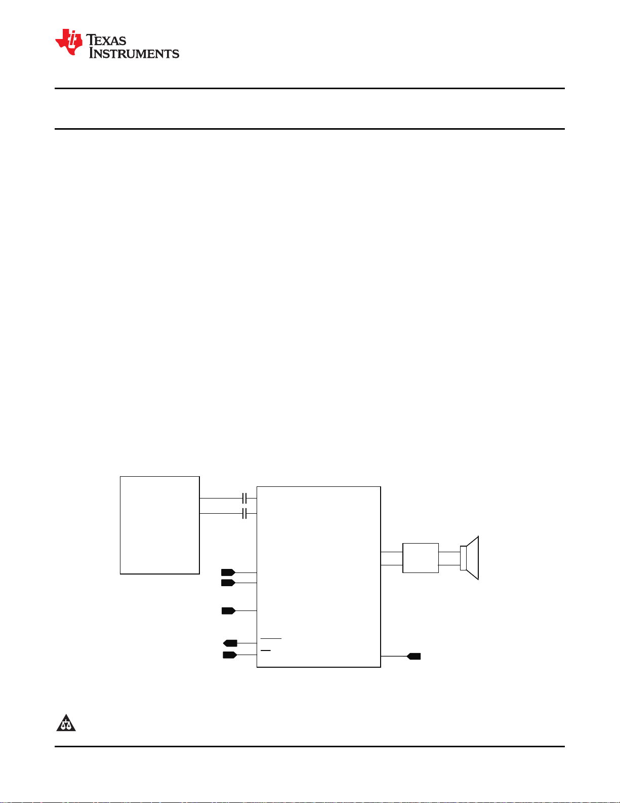
DESCRIPTION
The TPA3111D1 is a 10-W efficient, Class-D audio
power amplifier for driving a bridge tied speaker.
Advanced EMI Suppresion Technology enables the
use of inexpensive ferrite bead filters at the outputs
while meeting EMC requirements. SpeakerGuard™
speaker protection system includes an adjustable
power limiter and a DC detection circuit. The
adjustable power limiter allows the user to set a
"virtual" voltage rail lower than the chip supply to limit
the amount of current through the speaker. The DC
detect circuit measures the frequency and amplitude
of the PWM signal and shuts off the output stage if
the input capacitors are damaged or shorts exist on
the inputs.
The TPA3111D1 can drive a mono speaker as low as
4Ω. The high efficiency of the TPA3111D1, > 90%,
eliminates the need for an external heat sink when
playing music.
The outputs are fully protected against shorts to
GND, VCC, and output-to-output. The short-circuit
protection and thermal protection includes an autorecovery feature.
Figure 1. Simplified Application Diagram
1
Please be aware that an important notice concerning availability, standard warranty, and use in critical applications of
Texas Instruments semiconductor products and disclaimers thereto appears at the end of this data sheet.
2SpeakerGuard is a trademark of Texas Instruments.
PRODUCTION DATA information is current as of publication date.
Products conform to specifications per the terms of the Texas
Instruments standard warranty. Production processing does not
necessarily include testing of all parameters.
Copyright © 2009–2012, Texas Instruments Incorporated
Page 2
TPA3111D1
SLOS618E –AUGUST 2009–REVISED AUGUST 2012
www.ti.com
These devices have limited built-in ESD protection. The leads should be shorted together or the device placed in conductive foam
during storage or handling to prevent electrostatic damage to the MOS gates.
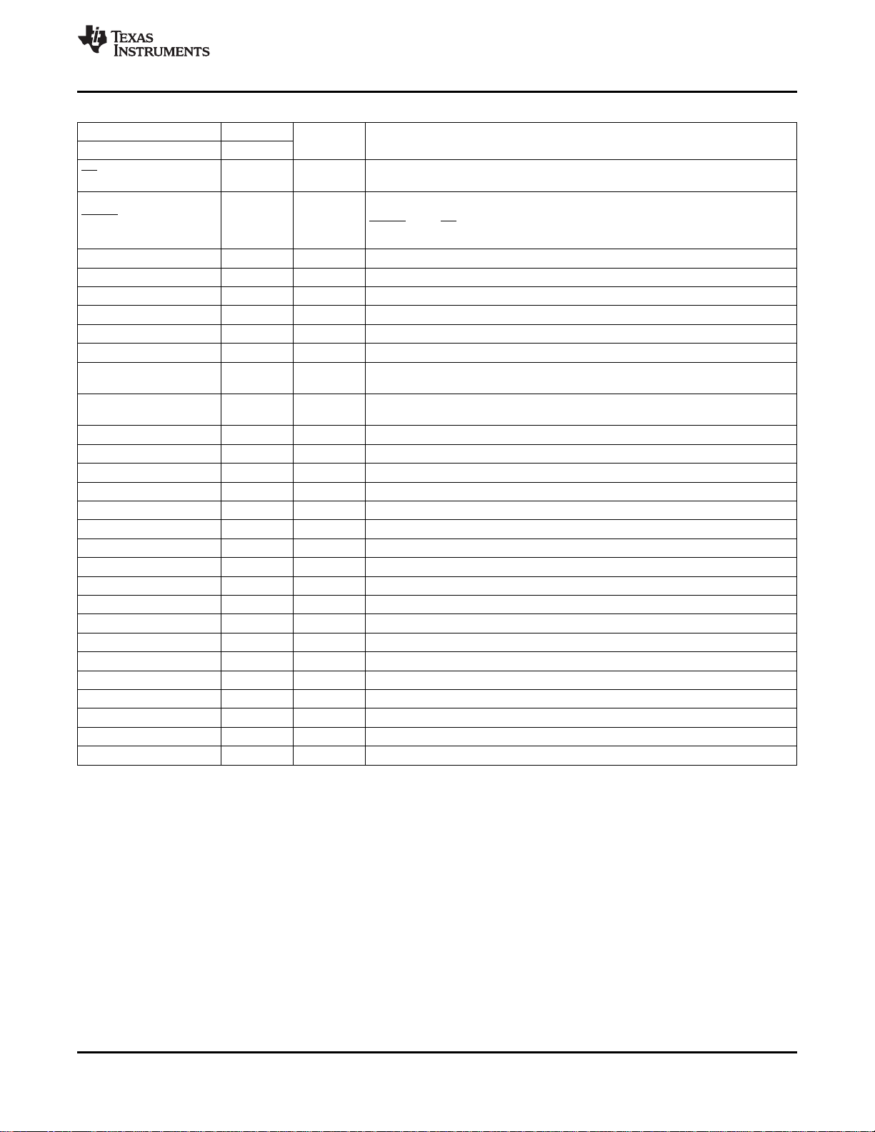
ABSOLUTE MAXIMUM RATINGS
over operating free-air temperature range (unless otherwise noted)
V
V
T
T
T
R
(1) Stresses beyond those listed under absolute maximum ratings may cause permanent damage to the device. These are stress ratings
(2) The voltage slew rate of these pins must be restricted to no more than 10 V/ms. For higher slew rates, use a 100 kΩ resister in series
(3) The TPA3111D1 incorporates an exposed thermal pad on the underside of the chip. This acts as a heatsink, and it must be connected
(4) In accordance with JEDEC Standard 22, Test Method A114-B.
(5) In accordance with JEDEC Standard 22, Test Method C101-A
Supply voltage AVCC, PVCC –0.3 V to 30 V
CC
SD, FAULT,GAIN0, GAIN1, AVCC (Pin 14)
Interface pin voltage
I
PLIMIT –0.3 V toGVDD + 0.3 V
INN, INP –0.3 V to 6.3 V
Continuous total power dissipation See Thermal Inforamtion Table
Operating free-air temperature range –40°C to 85°C
A
Operating junction temperature range
J
Storage temperature range –65°C to 150°C
stg
Minimum Load Resistance BTL 3.2
L
Electrostatic discharge
(3)
Human body model
Charged-device model
(4)
(all pins) ±2 kV
(5)
only, and functional operations of the device at these or any other conditions beyond those indicated under recommended operating
conditions is not implied. Exposure to absolute-maximum-rated conditions for extended periods may affect device reliability.
with the pins.
to a thermally dissipating plane for proper power dissipation. Failure to do so may result in the device going into thermal protection
shutdown. See TI Technical Briefs SCBA017D and SLUA271 for more information about using the QFN thermal pad. See TI Technical
Briefs SLMA002 for more information about using the HTQFP thermal pad.
(1)
UNIT
(2)
–0.3 V to VCC+ 0.3 V
< 10 V/ms
–40°C to 150°C
(all pins) ±500 V
THERMAL INFORMATION
(1) (2)
θ
θ
θ
ψ
ψ
θ
JA
JCtop
JB
JT
JB
JCbot
THERMAL METRIC
Junction-to-ambient thermal resistance 30.3
Junction-to-case (top) thermal resistance 33.5
Junction-to-board thermal resistance 17.5
Junction-to-top characterization parameter 0.9
Junction-to-board characterization parameter 7.2
Junction-to-case (bottom) thermal resistance 0.9
(1) For more information about traditional and new thermal metrics, see the IC Package Thermal Metrics application report, SPRA953.
(2) For thermal estimates of this device based on PCB copper area, see the TI PCB Thermal Calculator.
2 Submit Documentation Feedback Copyright © 2009–2012, Texas Instruments Incorporated
Product Folder Links: TPA3111D1
TPA3111D1
PWP (28 PINS)
UNITS
°C/W
Page 3
TPA3111D1
www.ti.com
SLOS618E –AUGUST 2009–REVISED AUGUST 2012
RECOMMENDED OPERATING CONDITIONS
over operating free-air temperature range (unless otherwise noted)
PARAMETER TEST CONDITIONS MIN MAX UNIT
V
V
V
V
I
I
T
Supply voltage PVCC, AVCC 8 26 V
CC
High-level input voltage SD, GAIN0, GAIN1 2 V
IH
Low-level input voltage SD, GAIN0, GAIN1 0.8 V
IL
Low-level output voltage FAULT, R
OL
High-level input current SD, GAIN0, GAIN1, VI= 2, VCC= 18 V 50 µA
IH
Low-level input current SD, GAIN0, GAIN1, VI= 0.8V, VCC= 18 V 5 µA
IL
Operating free-air temperature –40 85 °C
A
= 100kΩ, VCC=26V 0.8 V
PULLUP
DC CHARACTERISTICS
TA= 25°C, VCC= 24 V, RL= 8 Ω (unless otherwise noted)
PARAMETER TEST CONDITIONS MIN TYP MAX UNIT
| VOS| VI= 0 V, Gain = 36 dB 1.5 15 mV
I
CC
I
CC(SD)
r
DS(on)
G Gain
t
ON
t
OFF
GVDD Gate Drive Supply I
Class-D output offset voltage (measured
differentially)
Quiescent supply current SD = 2 V, no load, PVcc=21V 40 mA
Quiescent supply current in shutdown mode SD = 0.8 V, no load, PVcc=21V 400 µA
Drain-source on-state resistance mΩ
IO= 500 mA,
TJ= 25°C
GAIN1 = 0.8 V dB
GAIN1 = 2 V dB
High Side 240
Low side 240
GAIN0 = 0.8 V 19 20 21
GAIN0 = 2 V 25 26 27
GAIN0 = 0.8 V 31 32 33
GAIN0 = 2 V 35 36 37
Turn-on time SD = 2 V 10 ms
Turn-off time SD = 0.8 V 2 μs
= 2mA 6.5 6.9 7.3 V
GVDD
DC CHARACTERISTICS
TA= 25°C, VCC= 12 V, RL= 8 Ω (unless otherwise noted)
PARAMETER TEST CONDITIONS MIN TYP MAX UNIT
| VOS| VI= 0 V, Gain = 36 dB 1.5 15 mV
I
CC
I
CC(SD)
r
DS(on)
G Gain
t
ON
t
OFF
GVDD Gate Drive Supply I
PLIMIT Output Voltage maximum under PLIMIT V
Class-D output offset voltage (measured
differentially)
Quiescent supply current SD = 2 V, no load, PVcc=12V 20 mA
Quiescent supply current in shutdown mode SD = 0.8 V, no load, PVcc=12V 200 µA
Drain-source on-state resistance mΩ
IO= 500 mA,
TJ= 25°C
GAIN1 = 0.8 V dB
GAIN1 = 2 V dB
High Side 240
Low side 240
GAIN0 = 0.8 V 19 20 21
GAIN0 = 2 V 25 26 27
GAIN0 = 0.8 V 31 32 33
GAIN0 = 2 V 35 36 37
Turn-on time SD = 2 V 10 ms
Turn-off time SD = 0.8 V 2 μs
= 2mA 6.5 6.9 7.3 V
GVDD
=2.0 V; VI=6.0V differential 6.75 7.90 8.75 V
control
PLIMIT
Copyright © 2009–2012, Texas Instruments Incorporated Submit Documentation Feedback 3
Product Folder Links: TPA3111D1
Page 4
1
2
3
4
5
6
7
8
9
10
28
27
26
25
24
23
22
21
20
19
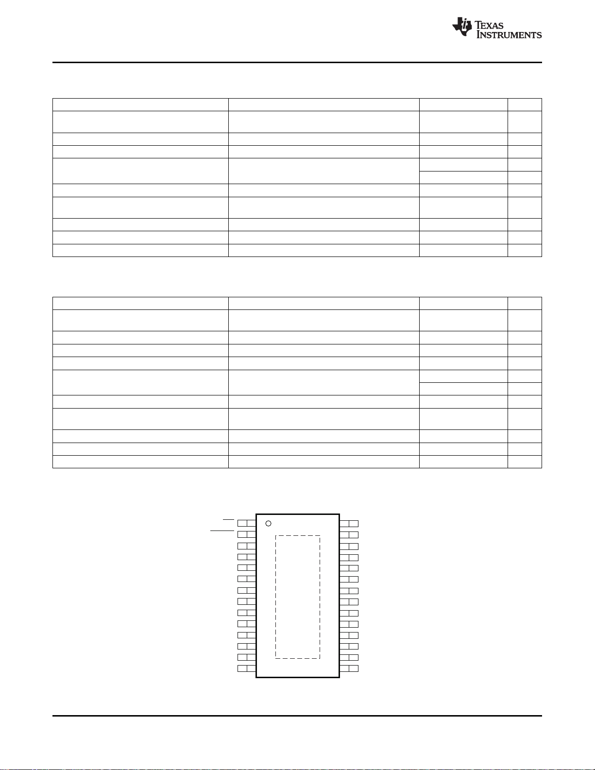
SD
FAULT
GND
GND
GAIN0
GAIN1
AVCC
AGND
GVDD
PLIMIT
PVCC
PVCC
BSN
OUTN
PGND
OUTN
BSN
BSP
OUTP
PGND
PWP (TSSOP)Package
(TopView)
INN
INP
NC
11
12
13
14
18
17
16
15
OUTP
BSP
PVCC
PVCC
AVCC
TPA3111D1
SLOS618E –AUGUST 2009–REVISED AUGUST 2012
www.ti.com
AC CHARACTERISTICS
TA= 25°C, VCC= 24 V, RL= 8 Ω (unless otherwise noted)
PARAMETER TEST CONDITIONS MIN TYP MAX UNIT
K
P
Power Supply ripple rejection –70 dB
SVR
Continuous output power THD+N ≤ 0.1%, f = 1 kHz, VCC= 24 V 10 W
O
THD+N Total harmonic distortion + noise VCC= 24 V, f = 1 kHz, PO= 5 W (half-power) <0.05 %
V
Output integrated noise 20 Hz to 22 kHz, A-weighted filter, Gain = 20 dB
n
Crosstalk VO= 1 Vrms, Gain = 20 dB, f = 1 kHz –70 dB
SNR Signal-to-noise ratio 102 dB
f
OSC
Oscillator frequency 250 310 350 kHz
Thermal trip point 150 °C
Thermal hysteresis 15 °C
200 mVPPripple from 20 Hz–1 kHz,
Gain = 20 dB, Inputs ac-coupled to AGND
65 µV
–80 dBV
Maximum output at THD+N < 1%, f = 1 kHz,
Gain = 20 dB, A-weighted
AC CHARACTERISTICS
TA= 25°C, VCC= 12 V, RL= 8 Ω (unless otherwise noted)
PARAMETER TEST CONDITIONS MIN TYP MAX UNIT
K
P
P
Supply ripple rejection –70 dB
SVR
Continuous output power THD+N ≤ 10%, f = 1 kHz , RL= 8Ω 10 W
O
Continuous output power THD+N ≤ 0.1%, f = 1 kHz , RL= 4Ω 10 W
O
THD+N Total harmonic distortion + noise RL= 8 Ω, f = 1 kHz, PO= 5 W (half-power) <0.06 %
V
Output integrated noise 20 Hz to 22 kHz, A-weighted filter, Gain = 20 dB
n
Crosstalk Po= 1 W, Gain = 20 dB, f = 1 kHz –70 dB
SNR Signal-to-noise ratio 102 dB
f
OSC
Oscillator frequency 250 310 350 kHz
Thermal trip point 150 °C
Thermal hysteresis 15 °C
200 mVPPripple from 20 Hz–1 kHz,
Gain = 20 dB, Inputs ac-coupled to AGND
65 µV
–80 dBV
Maximum output at THD+N < 1%, f = 1 kHz,
Gain = 20 dB, A-weighted
4 Submit Documentation Feedback Copyright © 2009–2012, Texas Instruments Incorporated
Product Folder Links: TPA3111D1
Page 5
TPA3111D1
www.ti.com
SLOS618E –AUGUST 2009–REVISED AUGUST 2012
PIN FUNCTIONS
PIN
NAME Pin #
SD 1 I
FAULT 2 O
GND 3 Connect to local ground
GND 4 Connect to local ground
GAIN0 5 I Gain select least significant bit. TTL logic levels with compliance to AVCC.
GAIN1 6 I Gain select most significant bit. TTL logic levels with compliance to AVCC.
AVCC 7 P Analog supply.
AGND 8 Analog supply ground. Connect to the thermal pad.
GVDD 9 O
PLIMIT 10 I
INN 11 I Negative audio input. Biased at 3V.
INP 12 I Positive audio input. Biased at 3V.
NC 13 Not connected
AVCC 14 P Connect AVCC supply to this pin
PVCC 15 P Power supply for H-bridge. PVCC pins are also connected internally.
PVCC 16 P Power supply for H-bridge. PVCC pins are also connected internally.
BSP 17 I Bootstrap I/O for positive high-side FET.
OUTP 18 O Class-D H-bridge positive output.
PGND 19 Power ground for the H-bridges.
OUTP 20 O Class-D H-bridge positive output.
BSP 21 I Bootstrap I/O for positive high-side FET.
BSN 22 I Bootstrap I/O for negative high-side FET.
OUTN 23 O Class-D H-bridge negative output.
PGND 24 Power ground for the H-bridges.
OUTN 25 O Class-D H-bridge negative output.
BSN 26 I Bootstrap I/O for negative high-side FET.
PVCC 27 P Power supply for H-bridge. PVCC pins are also connected internally.
PVCC 28 P Power supply for H-bridge. PVCC pins are also connected internally.
I/O DESCRIPTION
Shutdown logic input for audio amp(LOW = outputs Hi-Z, HIGH = outputs enabled).
TTL logic levels with compliance to AVCC.
Open drain output used to display short circuit or dc detect fault status. Voltage
compliant to AVCC. Short circuit faults can be set to auto-recovery by connecting
FAULT pin to SD pin. Otherwise bothe short circuit faults and dc detect faults must
be reset by cycling PVCC.
High-side FET gate drive supply. Nominal voltage is 7V. May also be used as
supply for PLILMIT divider. Add a 1μF cap to ground at this pin.
Power limit level adjust. Connect directly to GVDD pin for no power limiting. Add a
1μF cap to ground at this pin.
Copyright © 2009–2012, Texas Instruments Incorporated Submit Documentation Feedback 5
Product Folder Links: TPA3111D1
Page 6
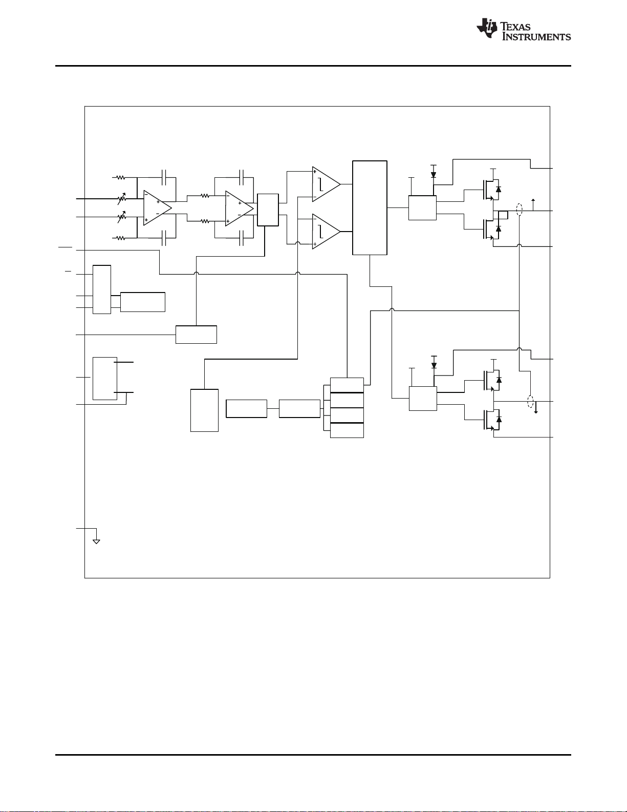
PWM
Logic
Gate
Drive
PVCC
PVCC
GVDD
BSP
PGND
OUTP
Gate
Drive
PVCC
PVCC
GVDD
BSN
PGND
OUTN
INP
INN
UVLO/OVLO
SC Detect
DC Detect
Thermal
Detect
Startup Protection
Logic
Biases and
References
FAULT
SD
GAIN0
PLIMIT
AGND
AVCC
GAIN1
Gain
Control
TTL
Buffer
Ramp
Generator
AVDD
GVDD
GVDD
LDO
Regulator
Gain
Control
PLIMIT
PLIMIT
Reference
OUTP FB
OUTN FB
OUTN FB
OUTP FB
TPA3111D1
SLOS618E –AUGUST 2009–REVISED AUGUST 2012
www.ti.com
FUNCTIONAL BLOCK DIAGRAM
6 Submit Documentation Feedback Copyright © 2009–2012, Texas Instruments Incorporated
Product Folder Links: TPA3111D1
Page 7
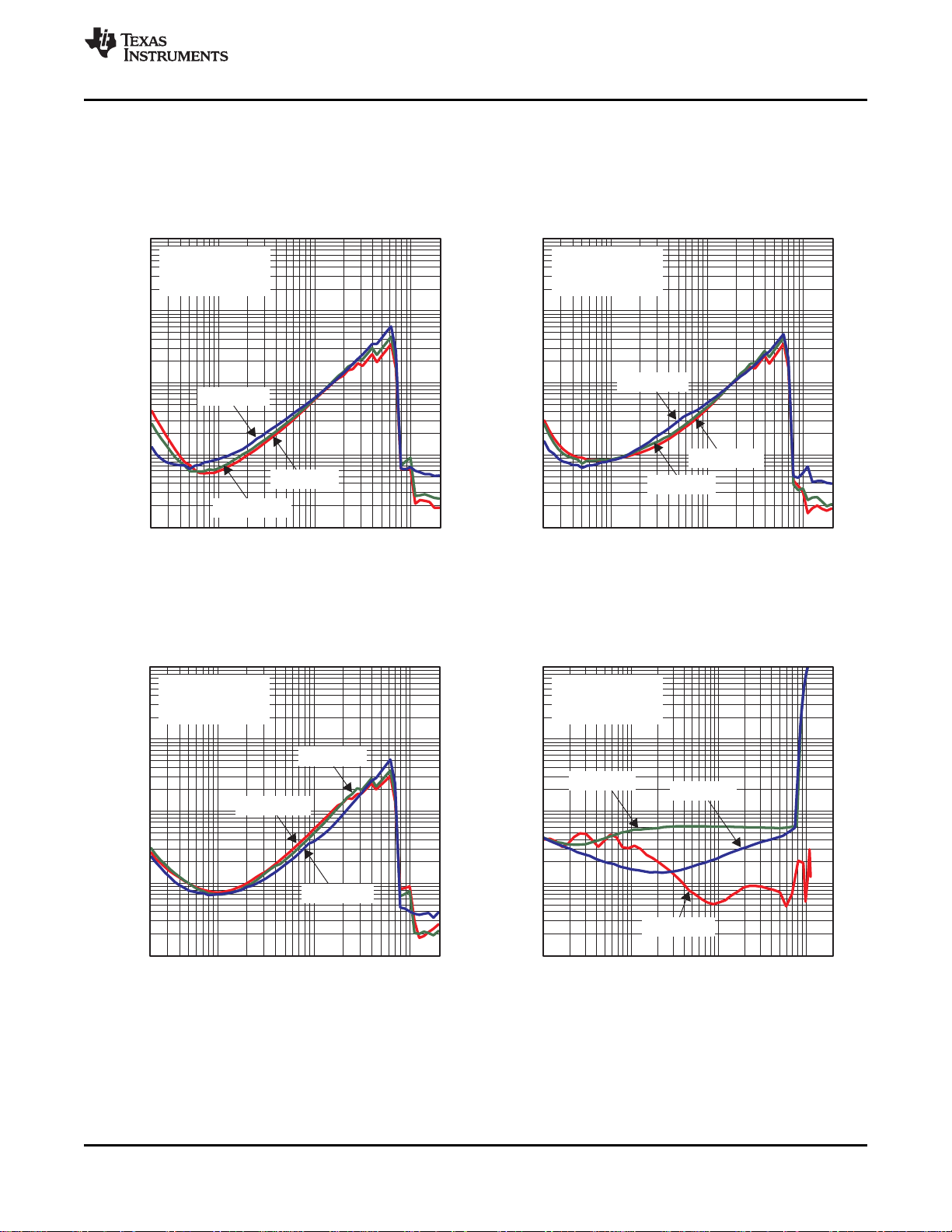
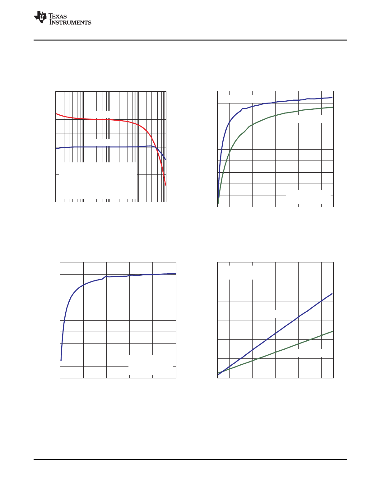
f − Frequency − Hz
20 100 1k 10k
THD − Total Harmonic Distortion − %
0.001
0.1
10
20k
0.01
1
G003
PO = 10 W
Gain = 20 dB
VCC = 12 V
ZL = 4 Ω + 33 µH
PO = 1 W
PO = 5 W
PO − Output Power − W
0.01 0.1 1 10
THD+N − Total Harmonic Distortion + Noise − %
0.001
0.1
10
20
0.01
1
G004
f = 1 kHz
Gain = 20 dB
VCC = 12 V
ZL = 8 Ω + 66 µH
f = 20 Hz
f = 10 kHz
f − Frequency − Hz
20 100 1k 10k
THD − Total Harmonic Distortion − %
0.001
0.1
10
20k
0.01
1
G001
PO = 2.5 W
PO = 5 W
Gain = 20 dB
VCC = 12 V
ZL = 8 Ω + 66 µH
PO = 1 W
f − Frequency − Hz
20 100 1k 10k
THD − Total Harmonic Distortion − %
0.001
0.1
10
20k
0.01
1
G002
Gain = 20 dB
VCC = 24 V
ZL = 8 Ω + 66 µH
PO = 10 W
PO = 5 W
PO = 1 W
TPA3111D1
www.ti.com
SLOS618E –AUGUST 2009–REVISED AUGUST 2012
TYPICAL CHARACTERISTICS
(All Measurements taken at 1 kHz, unless otherwise noted. Measurements were made using the TPA3110D2 EVM which is
available at ti.com.)
TOTAL HARMONIC DISTORTION TOTAL HARMONIC DISTORTION
vs vs
FREQUENCY FREQUENCY
Figure 2. Figure 3.
TOTAL HARMONIC DISTORTION TOTAL HARMONIC DISTORTION + NOISE
vs vs
FREQUENCY OUTPUT POWER
Figure 4. Figure 5.
Copyright © 2009–2012, Texas Instruments Incorporated Submit Documentation Feedback 7
Product Folder Links: TPA3111D1
Page 8
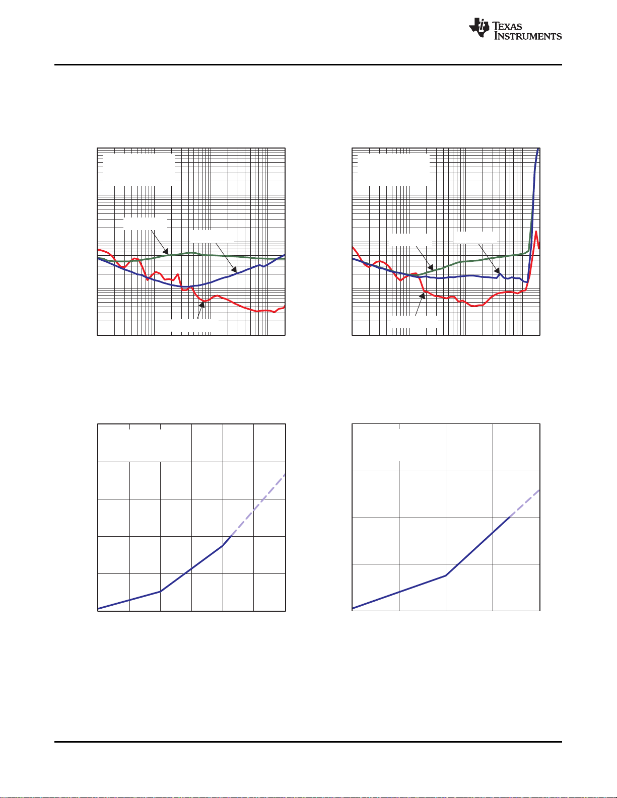
V
PLIMIT
− PLIMIT Voltage − V
0
5
10
15
20
25
0.0 0.5 1.0 1.5 2.0 2.5 3.0
P
O(Max)
− Maximum Output Power − W
G007
Gain = 20 dB
VCC = 24 V
ZL = 8 Ω + 66 µH
V
PLIMIT
− PLIMIT Voltage − V
0
5
10
15
20
0.0 0.5 1.0 1.5 2.0
P
O
− Output Power − W
G008
Gain = 20 dB
VCC = 12 V
ZL = 4 Ω + 33 µH
PO − Output Power − W
THD+N − Total Harmonic Distortion + Noise − %
0.001
0.1
10
0.01
1
G005
f = 1 kHz
Gain = 20 dB
VCC = 24 V
ZL = 8 Ω + 66 µH
f = 20 Hz
f = 10 kHz
0.01 0.1 1 10 20
0.01 0.1 1 10 20
PO − Output Power − W
THD+N − Total Harmonic Distortion + Noise − %
0.001
0.1
10
0.01
1
G006
f = 1 kHz
Gain = 20 dB
VCC = 12 V
ZL = 4 Ω + 33 µH
f = 20 Hz
f = 10 kHz
TPA3111D1
SLOS618E –AUGUST 2009–REVISED AUGUST 2012
www.ti.com
TYPICAL CHARACTERISTICS (continued)
(All Measurements taken at 1 kHz, unless otherwise noted. Measurements were made using the TPA3110D2 EVM which is
available at ti.com.)
TOTAL HARMONIC DISTORTION + NOISE TOTAL HARMONIC DISTORTION + NOISE
vs vs
OUTPUT POWER OUTPUT POWER
Figure 6. Figure 7.
MAXIMUM OUTPUT POWER OUTPUT POWER
vs vs
PLIMIT VOLTAGE PLIMIT VOLTAGE
Note: Dashed line represents thermally limited region.
Figure 8. Figure 9.
Note: Dashed line represents thermally limited region.
8 Submit Documentation Feedback Copyright © 2009–2012, Texas Instruments Incorporated
Product Folder Links: TPA3111D1
Page 9
PO − Output Power − W
0
10
20
30
40
50
60
70
80
90
100
0 1 2 3 4 5 6 7 8 9 10
η − Efficiency − %
G013
Gain = 20 dB
VCC = 12 V
ZL = 4 Ω + 33 µH
P
O(Tot)
− Total Output Power − W
0.0
0.2
0.4
0.6
0.8
1.0
1.2
0 1 2 3 4 5 6 7 8 9 10
I
CC
− Supply Current − A
G014
VCC = 12 V
VCC = 24 V
Gain = 20 dB
ZL = 8 Ω + 66 µH
PO − Output Power − W
0
10
20
30
40
50
60
70
80
90
100
0 1 2 3 4 5 6 7 8 9 10
η − Efficiency − %
G012
VCC = 24 V
Gain = 20 dB
ZL = 8 Ω + 66 µH
VCC = 12 V
f − Frequency − Hz
Phase − °
100
50
0
−300
0
5
10
15
20
25
30
35
40
Gain − dB
−50
−100
−150
10 100 10k 100k1k
G009
Phase
Gain
−200
−250
CI = 1 µF
Gain = 20 dB
Filter = Audio Precision AUX-0025
VCC = 12 V
VI = 0.1 Vrms
ZL = 8 Ω + 66 µH
TPA3111D1
www.ti.com
SLOS618E –AUGUST 2009–REVISED AUGUST 2012
TYPICAL CHARACTERISTICS (continued)
(All Measurements taken at 1 kHz, unless otherwise noted. Measurements were made using the TPA3110D2 EVM which is
available at ti.com.)
GAIN/PHASE EFFICIENCY
vs vs
FREQUENCY OUTPUT POWER
OUTPUT POWER TOTAL OUTPUT POWER
Copyright © 2009–2012, Texas Instruments Incorporated Submit Documentation Feedback 9
Figure 10. Figure 11.
EFFICIENCY SUPPLY CURRENT
vs vs
Figure 12. Figure 13.
Product Folder Links: TPA3111D1
Page 10

P
O(Tot)
− Total Output Power − W
0.0
0.2
0.4
0.6
0.8
1.0
1.2
0 1 2 3 4 5 6 7 8 9 10
I
CC
− Supply Current − A
G015
Gain = 20 dB
VCC = 12 V
ZL = 4 Ω + 33 µH
−120
−100
−80
−60
−40
−20
0
f − Frequency − Hz
K
SVR
− Supply Ripple Rejection Ratio − dB
20 100 1k 10k 20k
G016
Gain = 20 dB
VCC = 12 V
ZL = 8 Ω + 66 µH
TPA3111D1
SLOS618E –AUGUST 2009–REVISED AUGUST 2012
www.ti.com
TYPICAL CHARACTERISTICS (continued)
(All Measurements taken at 1 kHz, unless otherwise noted. Measurements were made using the TPA3110D2 EVM which is
available at ti.com.)
SUPPLY CURRENT SUPPLY RIPPLE REJECTION RATIO
vs vs
TOTAL OUTPUT POWER FREQUENCY
Figure 14. Figure 15.
DEVICE INFORMATION
Gain setting via GAIN0 and GAIN1 inputs
The gain of the TPA3111D1 is set by two input terminals, GAIN0 and GAIN1. The voltage slew rate of these gain
terminals, along with terminals 1 and 14, must be restricted to no more than 10V/ms. For higher slew rates, use
a 100kΩ resistor in series with the terminals.
The gains listed in Table 1 are realized by changing the taps on the input resistors inside the amplifier. This
causes the input impedance (ZI) to be dependent on the gain setting. The actual gain settings are controlled by
ratios of resistors, so the gain variation from part-to-part is small. However, the input impedance from part-to-part
at the same gain may shift by ±20% due to shifts in the actual resistance of the input resistors.
For design purposes, the input network (discussed in the next section) should be designed assuming an input
impedance of 7.2 kΩ, which is the absolute minimum input impedance of the TPA3111D1. At the lower gain
settings, the input impedance could increase as high as 72 kΩ
Table 1. Gain Setting
GAIN1 GAIN0
0 0 20 60
0 1 26 30
1 0 32 15
1 1 36 9
AMPLIFIER GAIN (dB)
TYP TYP
INPUT IMPEDANCE
(kΩ)
10 Submit Documentation Feedback Copyright © 2009–2012, Texas Instruments Incorporated
Product Folder Links: TPA3111D1
Page 11

TPA3111D1
www.ti.com
SLOS618E –AUGUST 2009–REVISED AUGUST 2012
SD OPERATION
The TPA3111D1 employs a shutdown mode of operation designed to reduce supply current (ICC) to the absolute
minimum level during periods of nonuse for power conservation. The SD input terminal should be held high (see
specification table for trip point) during normal operation when the amplifier is in use. Pulling SD low causes the
outputs to mute and the amplifier to enter a low-current state. Never leave SD unconnected, because amplifier
operation would be unpredictable.
For the best power-off pop performance, place the amplifier in the shutdown mode prior to removing the power
supply voltage.
PLIMIT
The voltage at pin 10 can used to limit the power to levels below that which is possible based on the supply rail.
Add a resistor divider from GVDD to ground to set the voltage at the PLIMIT pin. An external reference may also
be used if tighter tolerance is required. Also add a 1μF capacitor from pin 10 to ground.
The PLIMIT circuit sets a limit on the output peak-to-peak voltage. This limit can be thought of as a "virtual"
voltage rail which is lower than the supply connected to PVCC. This "virtual" rail is 4 times the voltage at the
PLIMIT pin. This output voltage can be used to calculate the maximum output power for a given maximum input
voltage and speaker impedance.
Figure 16. PLIMIT Circuit Operation
The PLIMIT circuits sets a limit on the output peak-to-peak voltage. The limiting is done by limiting the duty cycle
to fixed maximum value. This limit can be thought of as a “virtual” voltage rail which is lower than the supply
connected to PVCC. This “virtual” rail is 4 times the voltage at the PLIMIT pin. This output voltage can be used to
calculate the maximum output power for a given maximum input voltage and speaker impedance.
Copyright © 2009–2012, Texas Instruments Incorporated Submit Documentation Feedback 11
Product Folder Links: TPA3111D1
Page 12
2
2
2
L
P
L S
OUT
L
R
V
R R
P for unclipped power
R
æ ö
æ ö
´
ç ÷
ç ÷
ç ÷
+ ´
è ø
è ø
=
´
TPA3111D1
SLOS618E –AUGUST 2009–REVISED AUGUST 2012
Where:
RSis the total series resistance including R
, and any resistance in the output filter.
DS(on)
RLis the load resistance.
VPis the peak amplitude of the output possible within the supply rail.
VP= 4 × PLIMIT voltage if PLIMIT < 4 × V
P
(10%THD) = 1.25 × P
OUT
(unclipped)
OUT
P
Table 2. PLIMIT Typical Operation
Test Conditions () PLIMIT Voltage Output Power (W)
PVCC=24V, Vin=1Vrms,
RL=4Ω, Gain=20dB
PVCC=24V, Vin=1Vrms,
RL=4Ω, Gain=20dB
PVCC=12V, Vin=1Vrms,
RL=4Ω, Gain=20dB
PVCC=12V, Vin=1Vrms,
RL=4Ω, Gain=20dB
1.92 10 15.0
1.24 5 10.0
1.75 10 15.3
1.20 5 10.3
Output Voltage
Amplitude (V
P-P
www.ti.com
(1)
)
GVDD Supply
The GVDD Supply is used to power the gates of the output full bridge transistors. It can also used to supply the
PLIMIT voltage divider circuit. Add a 1μF capacitor to ground at this pin.
DC Detect
TPA3111D1 has circuitry which will protect the speakers from DC current which might occur due to defective
capacitors on the input or shorts on the printed circuit board at the inputs. A DC detect fault will be reported on
the FAULT pin as a low state. The DC Detect fault will also cause the amplifier to shutdown by changing the
state of the outputs to Hi-Z. To clear the DC Detect it is necessary to cycle the PVCC supply. Cycling SD will
NOT clear a DC detect fault.
A DC Detect Fault is issued when the output differential duty-cycle exceeds 14% (eg. +57%, -43%) for more than
420 ms at the same polarity. This feature protects the speaker from large DC currents or AC currents less than 2
Hz. To avoid nuisance faults due to the DC detect circuit, hold the SD pin low at power-up until the signals at the
inputs are stable. Also, take care to match the impedance seen at the positive and negative input to avoid
nuisance DC detect faults.
The minimum differential input voltages required to trigger the DC detect are shown in Table Table 3. The inputs
must remain at or above the voltage listed in the table for more than 420 ms to trigger the DC detect.
Table 3. DC Detect Threshold
AV(dB) Vin (mV, differential)
20 112
26 56
32 28
36 17
12 Submit Documentation Feedback Copyright © 2009–2012, Texas Instruments Incorporated
Product Folder Links: TPA3111D1
Page 13
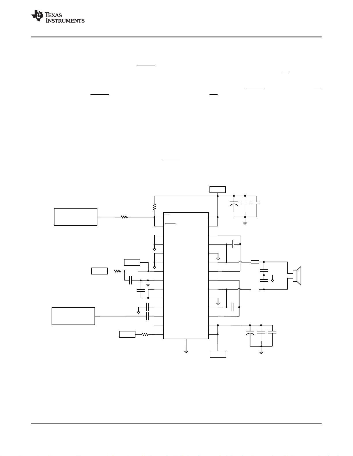
PVCC
PVCC
GAIN1
6
AVCC
7
8
AGND
9
GVDD
OUTN
BSN
BSP
OUTP
23
22
21
20
TPA3111D1
FAULT
2
GND
3
4
GND
5
GAIN0
PVCC
BSN
OUTN
PGND
27
26
25
24
PLIMIT
10
INN
11
12
INP
13
NC
PGND
OUTP
BSP
PVCC
19
18
17
16
AVCC
14
PVCC
15
GND
29
PowerPAD
SD
1
PVCC
28
PVCC
100 μF 0.1 μF
1000pF
100 Fμ
0.1 μF
1000pF
Audio
Source
Control
System
AVCC
100k Ω
10
100 kW
(1)
Ω
AVCC
1 kΩ
FB
FB
0.47 μF
1000 pF
0.47 μF
1000 pF
1 uF
1 uF
1 uF
1 uF
TPA3111D1
www.ti.com
SLOS618E –AUGUST 2009–REVISED AUGUST 2012
SHORT-CIRCUIT PROTECTION AND AUTOMATIC RECOVERY FEATURE
TPA3110D2 has protection from over-current conditions caused by a short circuit on the output stage. The short
circuit protection fault is reported on the FAULT pin as a low state. The amplifier outputs are switched to a Hi-Z
state when the short circuit protection latch is engaged. The latch can be cleared by cycling the SD pin through
the low state.
If automatic recovery from the short circuit protection latch is desired, connect the FAULT pin directly to the SD
pin. This will allow the FAULT pin function to automatically drive the SD pin low which will clear the short circuit
protection latch.
THERMAL PROTECTION
Thermal protection on the TPA3111D1 prevents damage to the device when the internal die temperature
exceeds 150°C. There is a ±15°C tolerance on this trip point from device to device. Once the die temperature
exceeds the thermal set point, the device enters into the shutdown state and the outputs are disabled. This is not
a latched fault. The thermal fault is cleared once the temperature of the die is reduced by 15°C. The device
begins normal operation at this point with no external system interaction.
Thermal protection faults are NOT reported on the FAULT terminal.
APPLICATION INFORMATION
(1) 100 kΩ resistor is needed if the PVCC slew rate is more than 10 V/ms.
Copyright © 2009–2012, Texas Instruments Incorporated Submit Documentation Feedback 13
Product Folder Links: TPA3111D1
Figure 17. Mono Class-D Amplifier with BTL Output
Page 14

0V
-12V
+12V
Current
OUTP
OUTN
Differential
Voltage
Across
Load
0V
-12V
+12V
Current
OUTP
OUTN
Differential
Voltage
Across
Load
Output=0V
Output>0V
TPA3111D1
SLOS618E –AUGUST 2009–REVISED AUGUST 2012
www.ti.com
CLASS-D OPERATION
This section focuses on the class-D operation of the TPA3111D1.
TPA3111D1 Modulation Scheme
The TPA3111D1 uses a modulation scheme that allows operation without the classic LC reconstruction filter
when the amp is driving an inductive load. Each output is switching from 0 volts to the supply voltage. The OUTP
and OUTN are in phase with each other with no input so that there is little or no current in the speaker. The duty
cycle of OUTP is greater than 50% and OUTN is less than 50% for positive output voltages. The duty cycle of
OUTP is less than 50% and OUTN is greater than 50% for negative output voltages. The voltage across the load
sits at 0 V throughout most of the switching period, greatly reducing the switching current, which reduces any I2R
losses in the load.
14 Submit Documentation Feedback Copyright © 2009–2012, Texas Instruments Incorporated
Figure 18. The TPA3111D1 Output Voltage and Current Waveforms Into an Inductive Load
Product Folder Links: TPA3111D1
Page 15

TPA3111D1
www.ti.com
SLOS618E –AUGUST 2009–REVISED AUGUST 2012
Ferrite Bead Filter Considerations
Using the Advanced Emissions Suppression Technology in the TPA3111D1 amplifier it is possible to design a
high efficiency Class-D audio amplifier while minimizing interference to surrounding circuits. it is also possible to
accomplishthis with only a low-cost ferrite bead filter. In this case it is necessary to carefully select the ferrite
bead used in the filter.
One important aspect of the ferrite bead selection is the type of material used in the ferrite bead. Not all ferrite
material is alike, so it is important to select a material that is effective in the 10 to 100 MHz range which is key to
the operation of the Class D amplifier. Many of the specifications regulating consumer electronics have
emissions limits as low as 30 MHz. It is important to use the ferrite bead filter to block radiation in the 30 MHz
and above range from appearing on the speaker wires and the power supply lines which are good antennas for
these signals. The impedance of the ferrite bead can be used along with a small capacitor with a value in the
range of 1000 pF to reduce the frequency spectrum of the signal to an acceptable level. For best performance,
the resonant frequency of the ferrite bead/ capacitor filter should be less than 10 MHz.
Also, it is important that the ferrite bead is large enough to maintain its impedance at the peak currents expected
for the amplifier. Some ferrite bead manufacturers specify the bead impedance at a variety of current levels. In
this case it is possible to make sure the ferrite bead maintains an adequate amount of impedance at the peak
current the amplifier will see. If these specifications are not available, it is also possible to estimate the bead
current handling capability by measuring the resonant frequency of the filter output at very low power and at
maximum power. A change of resonant frequency of less than fifty percent under this condition is desirable.
Examples of ferrite beads which have been tested and work well with the TPA3110D2 include 28L0138-80R-10
and HI1812V101R-10 from Steward and the 742792510 from Wurth Electronics.
A high quality ceramic capacitor is also needed for the ferrite bead filter. A low ESR capacitor with good
temperature and voltage characteristics will work best.
Additional EMC improvements may be obtained by adding snubber networks from each of the class D outputs to
ground. Suggested values for a simple RC series snubber network would be 10 ohms in series with a 330 pF
capacitor although design of the snubber network is specific to every application and must be designed taking
into account the parasitic reactance of the printed circuit board as well as the audio amp. Take care to evaluate
the stress on the component in the snubber network especially if the amp is running at high PVCC. Also, make
sure the layout of the snubber network is tight and returns directly to the PGND or the PowerPad beneath the
chip.
Efficiency: LC Filter Required With the Traditional Class-D Modulation Scheme
The main reason that the traditional class-D amplifier needs an output filter is that the switching waveform results
in maximum current flow. This causes more loss in the load, which causes lower efficiency. The ripple current is
large for the traditional modulation scheme, because the ripple current is proportional to voltage multiplied by the
time at that voltage. The differential voltage swing is 2 x VCC, and the time at each voltage is half the period for
the traditional modulation scheme. An ideal LC filter is needed to store the ripple current from each half cycle for
the next half cycle, while any resistance causes power dissipation. The speaker is both resistive and reactive,
whereas an LC filter is almost purely reactive.
The TPA3111D1 modulation scheme has little loss in the load without a filter because the pulses are short and
the change in voltage is VCCinstead of 2 x VCC. As the output power increases, the pulses widen, making the
ripple current larger. Ripple current could be filtered with an LC filter for increased efficiency, but for most
applications the filter is not needed.
An LC filter with a cutoff frequency less than the class-D switching frequency allows the switching current to flow
through the filter instead of the load. The filter has less resistance but higher impedance at the switching
frequency than the speaker, which results in less power dissipation, therefore increasing efficiency.
Copyright © 2009–2012, Texas Instruments Incorporated Submit Documentation Feedback 15
Product Folder Links: TPA3111D1
Page 16

1nF
Ferrite
ChipBead
OUTP
OUTN
Ferrite
ChipBead
1nF
2.2 mF
15 Hm
15 mH
OUTP
OUTN
L1
L2
C2
C3
2.2 mF
1 mF
1 mF
33 Hm
33 mH
OUTP
OUTN
L1
L2
C2
C3
TPA3111D1
SLOS618E –AUGUST 2009–REVISED AUGUST 2012
www.ti.com
When to Use an Output Filter for EMI Suppression
The TPA3111D1 has been tested with a simple ferrite bead filter for a variety of applications including long
speaker wires up to 125 cm and high power. The TPA3111D1 EVM passes FCC Class B specifications under
these conditions using twisted speaker wires. The size and type of ferrite bead can be selected to meet
applicaton requirements. Also, the filter capacitor can be increased if necessary with some impact on efficiency.
There may be a few circuit instances where it is necessary to add a complete LC reconstruction filter. These
circumstances might occur if there are nearby circuits which are very sensitive to noise. In these cases a classic
second order Butterworth filter similar to those shown in the figures below can be used.
Figure 19. Typical LC Output Filter, Cutoff Frequency of 27 kHz, Speaker Impedance = 8 Ω
Figure 20. Typical LC Output Filter, Cutoff Frequency of 27 kHz, Speaker Impedance = 4 Ω
Figure 21. Typical Ferrite Chip Bead Filter (Chip Bead Example: Steward HI0805R800R-10)
16 Submit Documentation Feedback Copyright © 2009–2012, Texas Instruments Incorporated
Product Folder Links: TPA3111D1
Page 17

C =
i
1
2 Z fp
i c
f =
c
1
2 Z Cp
i i
-3dB
f
c
f=
1
2 Z Cp
i i
C
i
IN
Z
i
Z
f
Input
Signal
TPA3111D1
www.ti.com
SLOS618E –AUGUST 2009–REVISED AUGUST 2012
INPUT RESISTANCE
Changing the gain setting can vary the input resistance of the amplifier from its smallest value, 9 kΩ ±20%, to the
largest value, 60 kΩ ±20%. As a result, if a single capacitor is used in the input high-pass filter, the -3 dB or
cutoff frequency may change when changing gain steps.
The -3-dB frequency can be calculated using Equation 2. Use the ZIvalues given in Table 1.
(2)
INPUT CAPACITOR, C
In the typical application, an input capacitor (CI) is required to allow the amplifier to bias the input signal to the
proper dc level for optimum operation. In this case, CIand the input impedance of the amplifier (ZI) form a highpass filter with the corner frequency determined in Equation 3.
I
The value of CIis important, as it directly affects the bass (low-frequency) performance of the circuit. Consider
the example where ZIis 60 kΩ and the specification calls for a flat bass response down to 20 Hz. Equation 3 is
reconfigured as Equation 4.
In this example, CIis 0.13 µF; so, one would likely choose a value of 0.15 μF as this value is commonly used. If
the gain is known and is constant, use ZIfrom Table 1 to calculate CI. A further consideration for this capacitor is
the leakage path from the input source through the input network (CI) and the feedback network to the load. This
leakage current creates a dc offset voltage at the input to the amplifier that reduces useful headroom, especially
in high gain applications. For this reason, a low-leakage tantalum or ceramic capacitor is the best choice. If a
ceramic capacitor is used, use a high quality capacitor with good temperature and voltage coefficient. An X7R
type works well and if possible use a higher voltage rating than required. This will give a better C vs voltage
characteristic. When polarized capacitors are used, the positive side of the capacitor should face the amplifier
input in most applications as the dc level there is held at 3 V, which is likely higher than the source dc level. Note
that it is important to confirm the capacitor polarity in the application. Additionally, lead-free solder can create dc
offset voltages and it is important to ensure that boards are cleaned properly.
Copyright © 2009–2012, Texas Instruments Incorporated Submit Documentation Feedback 17
Product Folder Links: TPA3111D1
(3)
(4)
Page 18

TPA3111D1
SLOS618E –AUGUST 2009–REVISED AUGUST 2012
POWER SUPPLY DECOUPLING, C
S
www.ti.com
The TPA3111D1 is a high-performance CMOS audio amplifier that requires adequate power supply decoupling
to ensure that the output total harmonic distortion (THD) is as low as possible. Power supply decoupling also
prevents oscillations for long lead lengths between the amplifier and the speaker.
Optimum decoupling is achieved by using a network of capacitors of different types that target specific types of
noise on the power supply leads. For higher frequency transients due to parasitic circuit elements such as bond
wire and copper trace inductances as well as lead frame capacitance, a good quality low equivalent-seriesresistance (ESR) ceramic capacitor of value between 220 pF and 1000 pF works well. This capacitor should be
placed as close to the device PVCC pins and system ground (either PGND pins or PowerPad) as possible. For
mid-frequency noise due to filter resonances or PWM switching transients as well as digital hash on the line,
another good quality capacitor typically 0.1 µF to 1 μF placed as close as possible to the device PVCC leads
works best For filtering lower frequency noise signals, a larger aluminum electrolytic capacitor of 220 µF or
greater placed near the audio power amplifier is recommended. The 220 µF capacitor also serves as a local
storage capacitor for supplying current during large signal transients on the amplifier outputs. The PVCC
terminals provide the power to the output transistors, so a 220 μF or larger capacitor should be placed on each
PVCC terminal. A 10 μF capacitor on the AVCC terminal is adequate. Also, a small decoupling resistor between
AVCC and PVCC can be used to keep high frequency class D noise from entering the linear input amplifiers.
BSN and BSP CAPACITORS
The full H-bridge output stage uses only NMOS transistors. Therefore, they require bootstrap capacitors for the
high side of each output to turn on correctly. A 470-nF ceramic capacitor, rated for at least 16 V, must be
connected from each output to its corresponding bootstrap input. Specifically, one 470-nF capacitor must be
connected from OUTP to BSP, and one 470-nF capacitor must be connected from OUTN to BSN. (See the
application circuit diagram in Figure 1.)
The bootstrap capacitors connected between the BSx pins and corresponding output function as a floating power
supply for the high-side N-channel power MOSFET gate drive circuitry. During each high-side switching cycle,
the bootstrap capacitors hold the gate-to-source voltage high enough to keep the high-side MOSFETs turned on.
DIFFERENTIAL INPUTS
The differential input stage of the amplifier cancels any noise that appears on both input lines of the channel. To
use the TPA3111D1 with a differential source, connect the positive lead of the audio source to the INP input and
the negative lead from the audio source to the INN input. To use the TPA3111D1 with a single-ended source, ac
ground the INP or INN input through a capacitor equal in value to the input capacitor on INN or INP and apply
the audio source to either input. In a single-ended input application, the unused input should be ac grounded at
the audio source instead of at the device input for best noise performance. For good transient performance, the
impedance seen at each of the two differential inputs should be the same.
The impedance seen at the inputs should be limited to an RC time constant of 1 ms or less if possible. This is to
allow the input dc blocking capacitors to become completely charged during the 14 msec power-up time. If the
input capacitors are not allowed to completely charge, there will be some additional sensitivity to component
matching which can result in pop if the input components are not well matched.
USING LOW-ESR CAPACITORS
Low-ESR capacitors are recommended throughout this application section. A real (as opposed to ideal) capacitor
can be modeled simply as a resistor in series with an ideal capacitor. The voltage drop across this resistor
minimizes the beneficial effects of the capacitor in the circuit. The lower the equivalent value of this resistance,
the more the real capacitor behaves like an ideal capacitor.
18 Submit Documentation Feedback Copyright © 2009–2012, Texas Instruments Incorporated
Product Folder Links: TPA3111D1
Page 19

TPA3111D1
www.ti.com
SLOS618E –AUGUST 2009–REVISED AUGUST 2012
PRINTED-CIRCUIT BOARD (PCB) LAYOUT
The TPA3111D1 can be used with a small, inexpensive ferrite bead output filter for most applications. However,
since the Class-D switching edges are very fast, it is necessary to take care when planning the layout of the
printed circuit board. The following suggestions will help to meet EMC requirements.
• Decoupling capacitors—The high-frequency decoupling capacitors should be placed as close to the PVCC
and AVCC terminals as possible. Large (220 μF or greater) bulk power supply decoupling capacitors should
be placed near the TPA3111D1 on the PVCC supplies. Local, high-frequency bypass capacitors should be
placed as close to the PVCC pins as possible. These caps can be connected to the thermal pad directly for
an excellent ground connection. Consider adding a small, good quality low ESR ceramic capacitor between
220 pF and 1000 pF and a larger mid-freqency cap of value between 0.1 µF and 1 µF also of good quality to
the PVCC connections at each end of the chip.
• Keep the current loop from each of the outputs through the ferrite bead and the small filter cap and back to
PGND as small and tight as possible. The size of this current loop determines its effectiveness as an
antenna.
• Output filter—The ferrite EMI filter (Figure 21) should be placed as close to the output terminals as possible
for the best EMI performance. The LC filter (Figure 19 and Figure 20) should be placed close to the outputs.
The capacitors used in both the ferrite and LC filters should be grounded to power ground.
• Thermal Pad—The thermal pad must be soldered to the PCB for proper thermal performance and optimal
reliability. The dimensions of the thermal pad and thermal land should be 6.46 mm by 2.35 mm. Seven rows
of solid vias (three vias per row, 0.33 mm or 13 mils diameter) should be equally spaced underneath the
thermal land. The vias should connect to a solid copper plane, either on an internal layer or on the bottom
layer of the PCB. The vias must be solid vias, not thermal relief or webbed vias. . See TI Application Report
SLMA002 for more information about using the TSSOP thermal pad. For recommended PCB footprints, see
mechanical pages appended to the end of this data sheet.
For an example layout, see the TPA3111D1 Evaluation Module (TPA3111D1EVM) User Manual. Both the EVM
user manual and the thermal pad application note are available on the TI Web site at http://www.ti.com.
spacer
REVISION HISTORY
Changes from Original (August 2009) to Revision A Page
• Added slew rate adjustment information ............................................................................................................................. 10
Changes from Revision A (July 2010) to Revision B Page
• Replaced the Dissipations Ratings Table with the Thermal Information Table .................................................................... 2
• In the BSN and BSP CAPACITORS section, the 220-nf capacitor rated for at least 25V was changed to a 470-nf
capacitor rated to at least 16V ............................................................................................................................................ 18
Changes from Revision B (August 2010) to Revision C Page
• Added < 10 V/ms to VIin the Absolute Maximum Ratings table .......................................................................................... 2
Changes from Revision C (October 2010) to Revision D Page
• Added a 100kΩ resistor to AVCC Pin 14 and Note 1 to Figure 17 .................................................................................... 13
Changes from Revision D (July 2012) to Revision E Page
• Changed 0.1 mF to 0.1 µF and 200 mF 200 µF in the POWER SUPPLY DECOUPLING, CSsection ............................. 18
• Changed 0.1 mF and 1 mF to 0.1 µF and 1 µF in the PRINTED-CIRCUIT BOARD (PCB) LAYOUT section .................. 19
Copyright © 2009–2012, Texas Instruments Incorporated Submit Documentation Feedback 19
Product Folder Links: TPA3111D1
Page 20

PACKAGE OPTION ADDENDUM
www.ti.com
23-Jul-2012
PACKAGING INFORMATION
Orderable Device
TPA3111D1PWP ACTIVE HTSSOP PWP 28 50 Green (RoHS
TPA3111D1PWPR ACTIVE HTSSOP PWP 28 2000 Green (RoHS
(1)
The marketing status values are defined as follows:
ACTIVE: Product device recommended for new designs.
LIFEBUY: TI has announced that the device will be discontinued, and a lifetime-buy period is in effect.
NRND: Not recommended for new designs. Device is in production to support existing customers, but TI does not recommend using this part in a new design.
PREVIEW: Device has been announced but is not in production. Samples may or may not be available.
OBSOLETE: TI has discontinued the production of the device.
Status
(1)
Package Type Package
Drawing
Pins Package Qty
Eco Plan
& no Sb/Br)
& no Sb/Br)
(2)
Lead/
Ball Finish
CU NIPDAU Level-3-260C-168 HR
CU NIPDAU Level-3-260C-168 HR
MSL Peak Temp
(3)
Samples
(Requires Login)
(2)
Eco Plan - The planned eco-friendly classification: Pb-Free (RoHS), Pb-Free (RoHS Exempt), or Green (RoHS & no Sb/Br) - please check http://www.ti.com/productcontent for the latest availability
information and additional product content details.
TBD: The Pb-Free/Green conversion plan has not been defined.
Pb-Free (RoHS): TI's terms "Lead-Free" or "Pb-Free" mean semiconductor products that are compatible with the current RoHS requirements for all 6 substances, including the requirement that
lead not exceed 0.1% by weight in homogeneous materials. Where designed to be soldered at high temperatures, TI Pb-Free products are suitable for use in specified lead-free processes.
Pb-Free (RoHS Exempt): This component has a RoHS exemption for either 1) lead-based flip-chip solder bumps used between the die and package, or 2) lead-based die adhesive used between
the die and leadframe. The component is otherwise considered Pb-Free (RoHS compatible) as defined above.
Green (RoHS & no Sb/Br): TI defines "Green" to mean Pb-Free (RoHS compatible), and free of Bromine (Br) and Antimony (Sb) based flame retardants (Br or Sb do not exceed 0.1% by weight
in homogeneous material)
(3)
MSL, Peak Temp. -- The Moisture Sensitivity Level rating according to the JEDEC industry standard classifications, and peak solder temperature.
Important Information and Disclaimer:The information provided on this page represents TI's knowledge and belief as of the date that it is provided. TI bases its knowledge and belief on information
provided by third parties, and makes no representation or warranty as to the accuracy of such information. Efforts are underway to better integrate information from third parties. TI has taken and
continues to take reasonable steps to provide representative and accurate information but may not have conducted destructive testing or chemical analysis on incoming materials and chemicals.
TI and TI suppliers consider certain information to be proprietary, and thus CAS numbers and other limited information may not be available for release.
In no event shall TI's liability arising out of such information exceed the total purchase price of the TI part(s) at issue in this document sold by TI to Customer on an annual basis.
OTHER QUALIFIED VERSIONS OF TPA3111D1 :
Automotive: TPA3111D1-Q1
•
NOTE: Qualified Version Definitions:
Addendum-Page 1
Page 21

PACKAGE OPTION ADDENDUM
www.ti.com
Automotive - Q100 devices qualified for high-reliability automotive applications targeting zero defects
•
23-Jul-2012
Addendum-Page 2
Page 22

PACKAGE MATERIALS INFORMATION
www.ti.com 23-Jul-2012
TAPE AND REEL INFORMATION
*All dimensions are nominal
Device Package
TPA3111D1PWPR HTSSOP PWP 28 2000 330.0 16.4 6.9 10.2 1.8 12.0 16.0 Q1
Type
Package
Drawing
Pins SPQ Reel
Diameter
(mm)
Reel
Width
W1 (mm)
A0
(mm)B0(mm)K0(mm)P1(mm)W(mm)
Pin1
Quadrant
Pack Materials-Page 1
Page 23

PACKAGE MATERIALS INFORMATION
www.ti.com 23-Jul-2012
*All dimensions are nominal
Device Package Type Package Drawing Pins SPQ Length (mm) Width (mm) Height (mm)
TPA3111D1PWPR HTSSOP PWP 28 2000 367.0 367.0 38.0
Pack Materials-Page 2
Page 24

Page 25

Page 26

Page 27

IMPORTANT NOTICE
Texas Instruments Incorporated and its subsidiaries (TI) reserve the right to make corrections, enhancements, improvements and other
changes to its semiconductor products and services per JESD46C and to discontinue any product or service per JESD48B. Buyers should
obtain the latest relevant information before placing orders and should verify that such information is current and complete. All
semiconductor products (also referred to herein as “components”) are sold subject to TI’s terms and conditions of sale supplied at the time
of order acknowledgment.
TI warrants performance of its components to the specifications applicable at the time of sale, in accordance with the warranty in TI’s terms
and conditions of sale of semiconductor products. Testing and other quality control techniques are used to the extent TI deems necessary
to support this warranty. Except where mandated by applicable law, testing of all parameters of each component is not necessarily
performed.
TI assumes no liability for applications assistance or the design of Buyers’ products. Buyers are responsible for their products and
applications using TI components. To minimize the risks associated with Buyers’ products and applications, Buyers should provide
adequate design and operating safeguards.
TI does not warrant or represent that any license, either express or implied, is granted under any patent right, copyright, mask work right, or
other intellectual property right relating to any combination, machine, or process in which TI components or services are used. Information
published by TI regarding third-party products or services does not constitute a license to use such products or services or a warranty or
endorsement thereof. Use of such information may require a license from a third party under the patents or other intellectual property of the
third party, or a license from TI under the patents or other intellectual property of TI.
Reproduction of significant portions of TI information in TI data books or data sheets is permissible only if reproduction is without alteration
and is accompanied by all associated warranties, conditions, limitations, and notices. TI is not responsible or liable for such altered
documentation. Information of third parties may be subject to additional restrictions.
Resale of TI components or services with statements different from or beyond the parameters stated by TI for that component or service
voids all express and any implied warranties for the associated TI component or service and is an unfair and deceptive business practice.
TI is not responsible or liable for any such statements.
Buyer acknowledges and agrees that it is solely responsible for compliance with all legal, regulatory and safety-related requirements
concerning its products, and any use of TI components in its applications, notwithstanding any applications-related information or support
that may be provided by TI. Buyer represents and agrees that it has all the necessary expertise to create and implement safeguards which
anticipate dangerous consequences of failures, monitor failures and their consequences, lessen the likelihood of failures that might cause
harm and take appropriate remedial actions. Buyer will fully indemnify TI and its representatives against any damages arising out of the use
of any TI components in safety-critical applications.
In some cases, TI components may be promoted specifically to facilitate safety-related applications. With such components, TI’s goal is to
help enable customers to design and create their own end-product solutions that meet applicable functional safety standards and
requirements. Nonetheless, such components are subject to these terms.
No TI components are authorized for use in FDA Class III (or similar life-critical medical equipment) unless authorized officers of the parties
have executed a special agreement specifically governing such use.
Only those TI components which TI has specifically designated as military grade or “enhanced plastic” are designed and intended for use in
military/aerospace applications or environments. Buyer acknowledges and agrees that any military or aerospace use of TI components
which have not been so designated is solely at the Buyer's risk, and that Buyer is solely responsible for compliance with all legal and
regulatory requirements in connection with such use.
TI has specifically designated certain components which meet ISO/TS16949 requirements, mainly for automotive use. Components which
have not been so designated are neither designed nor intended for automotive use; and TI will not be responsible for any failure of such
components to meet such requirements.
Products Applications
Audio www.ti.com/audio Automotive and Transportation www.ti.com/automotive
Amplifiers amplifier.ti.com Communications and Telecom www.ti.com/communications
Data Converters dataconverter.ti.com Computers and Peripherals www.ti.com/computers
DLP® Products www.dlp.com Consumer Electronics www.ti.com/consumer-apps
DSP dsp.ti.com Energy and Lighting www.ti.com/energy
Clocks and Timers www.ti.com/clocks Industrial www.ti.com/industrial
Interface interface.ti.com Medical www.ti.com/medical
Logic logic.ti.com Security www.ti.com/security
Power Mgmt power.ti.com Space, Avionics and Defense www.ti.com/space-avionics-defense
Microcontrollers microcontroller.ti.com Video and Imaging www.ti.com/video
RFID www.ti-rfid.com
OMAP Mobile Processors www.ti.com/omap TI E2E Community e2e.ti.com
Wireless Connectivity www.ti.com/wirelessconnectivity
Mailing Address: Texas Instruments, Post Office Box 655303, Dallas, Texas 75265
Copyright © 2012, Texas Instruments Incorporated
Page 28

 Loading...