

Page 1
SLOS406A − FEBRUARY 2003 − REVISED MARCH 2003
Please be aware that an important notice concerning availability, standard warranty, and use in critical applications of Texas Instruments
FEATURES
D
3-W/Ch Into an 8-Ω Load From 12-V Supply
D Efficient, Class-D Operation Eliminates
Heatsinks and Reduces Power Supply
Requirements
D 32-Step DC Volume Control From −40 dB
to 36 dB
D Third Generation Modulation Techniques
− Replaces Large LC Filter With Small
Low-Cost Ferrite Bead Filter
D Thermal and Short-Circuit Protection
APPLICATIONS
D
LCD Monitors and TVs
D Powered Speakers
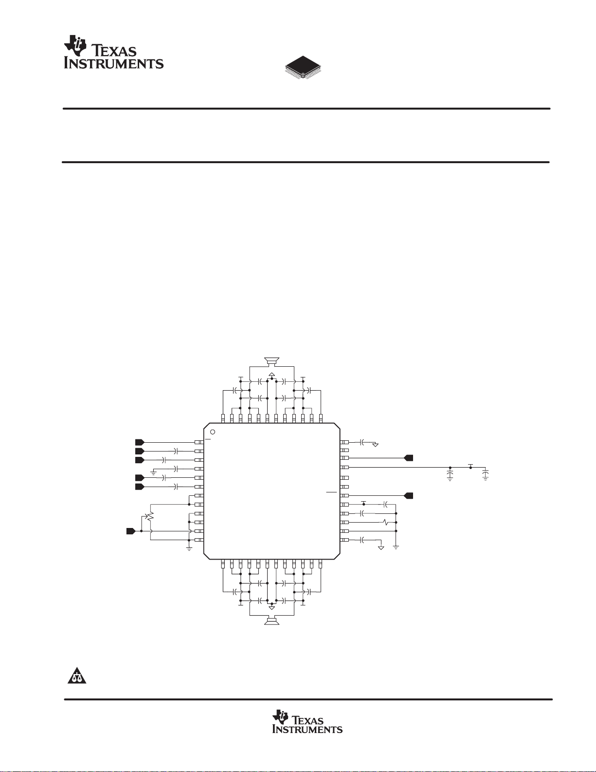
PVCC PVCC
10 nF
Cs
0.1 µF
Cbs
Cs
BSRN
PVCCR
PVCCR
ROUTN
BSLN
PVCCL
PVCCL
ROUTN
TPA3003D2
LOUTN
LOUTN
SYSTEM CONTROL
RINN
RINP
LINP
LINN
VOLUME
Crinp
1 µF
Clinp
1 µF
Crinn
1 µF
C2p5
1 µF
Clinn
1 µF
RINN
RINP
V2P5
LINP
LINN
AVDDREF
VREF
AGND
AGND
VOLUME
REFGND
PGNDR
PGNDL
10 µF10 µF
Cs
0.1 µF
Cs
PGNDR
PGNDL
ROUTP
LOUTP
DESCRIPTION
The TPA3003D2 is a 3-W (per channel) efficient,
Class-D audio amplifier for driving bridged-tied stereo
speakers. The TPA3003D2 can drive stereo speakers
as low as 8 Ω. The high efficiency of the TPA3003D2
eliminates the need for external heatsinks when playing
music.
Stereo speaker volume is controlled with a dc voltage
applied to the volume control terminal offering a range
of gain from –40 dB to 36 dB.
10 nF
Cbs
ROUTP
LOUTP
PVCCR
PVCCL
PVCCR
VCLAMPRSD
VCLAMPL
PVCCL
BSRP
MUTE
AVCC
FADE
AVDD
COSC
ROSC
AGND
BSLP
Ccpr
1 µF
NC
NC
NC
AVDD
Cvdd
Cosc
100 nF
Rosc
220 pF
120 kΩ
Ccpl
1 µF
MUTE CONTROL
SYSTEM CONTROL
Cs
0.1 µF
AVCC
Cvcc
10 µF
Cbs
0.1 µF
Cs
10 nF
10 µF
PVCC PVCC
0.1 µF
Cs
10 µF
Cbs
10 nF
Cs
Cs
semiconductor products and disclaimers thereto appears at the end of this data sheet.
!"# $"%&! '#(
'"! ! $#!! $# )# # #* "#
'' +,( '"! $!#- '# #!#&, !&"'#
#- && $##(
Copyright 2003, Texas Instruments Incorporated
www.ti.com
1
Page 2

T
SLOS406A − FEBRUARY 2003 − REVISED MARCH 2003
−40°C to 85°C TPA3003D2PFB
†
The PFB package is available taped and reeled. To order a taped and
reeled part, add the suffix R to the part number (e.g., TPA3003D2PFBR).
BSRN
48 47 46 45 44 43 42 41 40 39 38 37
A
PVCCR
AVAILABLE OPTIONS
PHP PACKAGE
(TOP VIEW)
PVCCR
ROUTN
ROUTN
PGNDR
PACKAGED DEVICE
48-PIN TQFP (PFB)
PGNDR
ROUTP
ROUTP
PVCCR
PVCCR
†
BSRP
SD
RINN
RINP
V2P5
LINP
LINN
AVDDREF
VREF
AGND
AGND
VOLUME
REFGND
1
2
3
4
5
6
7
8
9
10
11
12
TPA3003D2
13
14 15 16 17 18 19 20 21 22 23 24
BSLN
PVCCL
PVCCL
LOUTN
LOUTN
PGNDL
LOUTP
PGNDL
LOUTP
PVCCL
PVCCL
36
35
34
33
32
31
30
29
28
27
26
25
BSLP
VCLAMPR
NC
MUTE
AV
CC
NC
NC
FADE
AV
DD
COSC
ROSC
AGND
VCLAMPL
2
www.ti.com
Page 3
)
functional block diagram
V2P5
V2P5
RINN
RINP
VREF
VOLUME
FADE
REFGND
ROSC
COSC
AVDDREF
AVDD
SD
MUTE
V2P5
Gain
Gain
Control
Adj.
TTL Input
Buffer
AVDD
To Gain Adj.
Blocks
Ramp
Generator
5V LDO
V2P5
Biases
References
SLOS406A − FEBRUARY 2003 − REVISED MARCH 2003
PVCC
VClamp
Gen
Gate
Drive
Deglitch &
Modulation
Logic
Gate
Drive
Short Circuit
Detect
Startup
PVCC
VClamp
Gen
Protection
Logic
&
Thermal
VDDok
VCCok
VDD
AVCC
VCLAMPR
BSRN
PVCCR(2)
ROUTN(2
PGNDR
BSRP
PVCCR(2)
ROUTP(2)
PGNDR
AVCC
AGND
VCLAMPL
BSLN
PVCCL(2)
LINN
LINP
V2P5
Gain
Adj.
Rfdbk2
Rfdbk2
Cint2
Cint2
www.ti.com
Deglitch &
Modulation
Logic
Gate
Drive
Gate
Drive
LOUTN(2)
PGNDL
BSLP
PVCCL(2)
LOUTP(2)
PGNDL
3
Page 4
I/O
DESCRIPTION
SLOS406A − FEBRUARY 2003 − REVISED MARCH 2003
Terminal Functions
TERMINAL
NO. NAME
AGND 9, 10, 26 − Analog ground for digital/analog cells in core
AV
CC
AV
DD
AVDDREF 7 O 5-V Reference output—provided for connection to adjacent VREF terminal.
BSLN 13 I/O Bootstrap I/O for left channel, negative high-side FET
BSLP 24 I/O Bootstrap I/O for left channel, positive high-side FET
BSRN 48 I/O Bootstrap I/O for right channel, negative high-side FET
BSRP 37 I/O Bootstrap I/O for right channel, positive high-side FET
COSC 28 I/O I/O for charge/discharging currents onto capacitor for ramp generator triangle wave biased at V2P5
FADE 30 I Input for controlling volume ramp rate when cycling SD or during power-up. A logic low on this pin places
LINN 6 I Negative differential audio input for left channel
LINP 5 I Positive differential audio input for left channel
LOUTN 16, 17 O Class-D 1/2-H-bridge negative output for left channel
LOUTP 20, 21 O Class-D 1/2-H-bridge positive output for left channel
MUTE 34 I A logic high on this pin disables the outputs. A low on this pin enables the outputs.
NC 31, 32,
PGNDL 18, 19 − Power ground for left channel H-bridge
PGNDR 42, 43 − Power ground for right channel H-bridge
PVCCL 14, 15 − Power supply for left channel H-bridge (tied to pins 22 and 23 internally), not connected to PVCCR or
PVCCL 22, 23 − Power supply for left channel H-bridge (tied to pins 14 and 15 internally), not connected to PVCCR or
PVCCR 38,39 − Power supply for right channel H-bridge (tied to pins 46 and 47 internally), not connected to PVCCL or
PVCCR 46, 47 − Power supply for right channel H-bridge (tied to pins 38 and 39 internally), not connected to PVCCL or
REFGND 12 − Ground for gain control circuitry. Connect to AGND. If using a DAC to control the volume, connect the DAC
RINP 3 I Positive differential audio input for right channel
RINN 2 I Negative differential audio input for right channel
ROSC 27 I/O Current setting resistor for ramp generator. Nominally equal to 1/8*V
ROUTN 44, 45 O Class-D 1/2-H-bridge negative output for right channel
ROUTP 40, 41 O Class-D 1/2-H-bridge positive output for right channel
SD 1 I Shutdown signal for IC (low = shutdown, high = operational). TTL logic levels with compliance to VCC.
VCLAMPL 25 − Internally generated voltage supply for left channel bootstrap capacitors.
VCLAMPR 36 − Internally generated voltage supply for right channel bootstrap capacitors.
VOLUME 11 I DC voltage that sets the gain of the amplifier.
VREF 8 I Analog reference for gain control section.
V2P5 4 O 2.5-V Reference for analog cells, as well as reference for unused audio input when using single-ended
33 − High-voltage analog power supply (8.5 V to 14 V)
29 O 5-V Regulated output
the amplifier in fade mode. A logic high on this pin allows a quick transition to the desired volume setting.
− Not internally connected
35
AVCC.
AVCC.
AVCC.
AVCC.
ground to this terminal.
CC
inputs.
4
www.ti.com
Page 5
IH
High-level input voltage, V
IH
V
IL
Low-level input voltage, V
IL
V
IH
High-level input current, I
IH
µA
IL
SLOS406A − FEBRUARY 2003 − REVISED MARCH 2003
absolute maximum ratings over operating free-air temperature range (unless otherwise noted)
Supply voltage range: AV
Input voltage range, V
: MUTE, VREF, VOLUME, FADE 0 V to 5.5 V. . . . . . . . . . . . . . . . . . . . . . . . . . . . . . . . . . . . . . . .
I
Supply current, AV
Continuous total power dissipation See Dissipation Rating Table. . . . . . . . . . . . . . . . . . . . . . . . . . . . . . . . . . . . . . . . . .
Operating free-air temperature range, T
Operating junction temperature range, T
Storage temperature range, T
Lead temperature 1,6 mm (1/16 inch) from case for 10 seconds 260°C. . . . . . . . . . . . . . . . . . . . . . . . . . . . . . . . . . . . .
†
Stresses beyond those listed under “absolute maximum ratings” may cause permanent damage to the device. These are stress ratings only , a nd
functional operation of the device at these or any other conditions beyond those indicated under “recommended operating conditions” is not
implied. Exposure to absolute-maximum-rated conditions for extended periods may affect device reliability.
PACKAGE
PFB 2.8 W 22.2 mW/°C 1.8 W 1.4 W
recommended operating conditions
Supply voltage, V
Volume reference voltage VREF 3.0 5.5 V
Volume control pins, input voltage VOLUME 5.5 V
High-level input voltage, V
Low-level input voltage, V
High-level input current, I
Low-level input current, I
Oscillator frequency, f
Operating free-air temperature, T
CC
OSC
SD
CC,
PV
CC
−0.3 V to VCC + 0.3 V. . . . . . . . . . . . . . . . . . . . . . . . . . . . . . . . . . . . . . . . . . . . . . . . . . . . . . . .
−0.3 V to 15 V. . . . . . . . . . . . . . . . . . . . . . . . . . . . . . . . . . . . . . . . . . . . . . . . . . . . .
RINN, RINP, LINN, LINP −0.3 V to 7 V. . . . . . . . . . . . . . . . . . . . . . . . . . . . . . . . . . . . . . . . . . . .
DD
AVDDREF 10 mA. . . . . . . . . . . . . . . . . . . . . . . . . . . . . . . . . . . . . . . . . . . . . . . . . . . . . . . . . . . . . .
A
J
stg
DISSIPATION RATING TABLE
TA ≤ 25°C DERATING FACTOR TA = 70°C TA = 85°C
PVCC, AV
SD 2
MUTE 3.5
FADE 4
SD 0.8
MUTE 2
FADE 2
MUTE, VI= 5 V, VCC = 14 V 1
SD, VI= 14 V, VCC = 14 V 50
FADE, VI= 5 V, VCC = 14 V 150
MUTE, SD, FADE, VI= 0 V, VCC = 14 V 1 µA
A
CC
225 275 kHz
−40 85 °C
MIN MAX UNIT
8.5 14 V
−40°C to 85°C. . . . . . . . . . . . . . . . . . . . . . . . . . . . . . . . . . . . . . . . . . . . . . . . . .
−40°C to 150°C. . . . . . . . . . . . . . . . . . . . . . . . . . . . . . . . . . . . . . . . . . . . . . . .
−65°C to 150°C. . . . . . . . . . . . . . . . . . . . . . . . . . . . . . . . . . . . . . . . . . . . . . . . . . . . . . . .
10 mA. . . . . . . . . . . . . . . . . . . . . . . . . . . . . . . . . . . . . . . . . . . . . . . . . . . . . . . . . . . . . . . . . .
V
V
µA
†
www.ti.com
5
Page 6
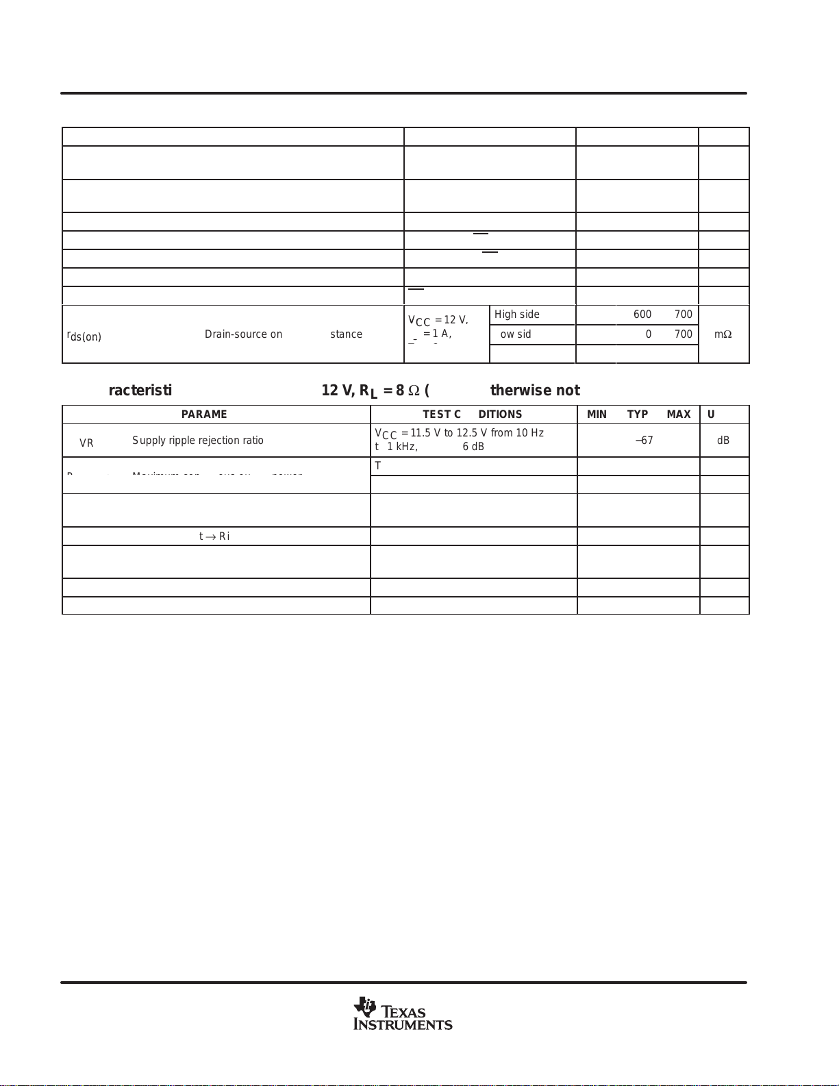
V
= 12 V,
VCC = 12 V,
r
ds(on)
Drain-source on-state resistance
IO = 1 A,
m
SLOS406A − FEBRUARY 2003 − REVISED MARCH 2003
dc characteristics, T
| VOS |
V2P5 (terminal 4) 2.5-V Bias voltage No load
PSRR Power supply rejection ratio VCC = 11.5 V to 12.5 V −80 dB
I
CC
I
CC(MUTE)
I
CC(max power)
I
CC(SD)
r
ds(on)
ac characteristics, T
k
SVR
P
O(max)
V
n
SNR Signal-to-noise ratio
Supply ripple rejection ratio
Maximum continuous output power
Output integrated noise floor
Crosstalk, Left → Right Gain = 13.2 dB, PO = 1 W, RL = 8 Ω −77 dB
Thermal trip point 150 °C
Thermal hystersis 20 °C
= 25°C, VCC = 12 V, RL = 8 Ω (unless otherwise noted)
A
PARAMETER
Output offset voltage (measured
differentially)
Supply quiescent current MUTE = 2 V, SD = 2 V 16 28.5 mA
MUTE mode quiescent current MUTE = 3.5 V, SD = 2 V 7 9 mA
Supply current at max power RL = 8 Ω, PO = 3 W 0.6 A
Supply current in shutdown mode SD = 0.8 V 1 10 µA
Drain-source on-state resistance
= 25°C, VCC = 12 V, RL = 8 Ω (unless otherwise noted)
A
PARAMETER TEST CONDITIONS MIN TYP MAX UNITS
VCC = 11.5 V to 12.5 V from 10 Hz
to 1 kHz, Gain = 36 dB
THD+N = 1%, f = 1 kHz, RL = 8 Ω 3 W
THD+N = 10%, f = 1 kHz, RL = 8 Ω
20 Hz to 22 kHz, No weighting filter,
Gain = 0.5 dB
Maximum output at THD+N < 0.5%,
f= 1 kHz, Gain = 0.5 dB
TEST CONDITIONS MIN TYP MAX UNIT
INN and INP connected together,
Gain = 36 dB
High side
IO = 1 A,
TJ = 25°C
Low side
Total
0.45x
AV
DD
10 65 mV
0.5x
AV
AV
DD
600
600
1200
−67 dB
3.75 W
−82 dBV
102 dB
0.55x
DD
700
700
1400
V
mΩ
6
www.ti.com
Page 7
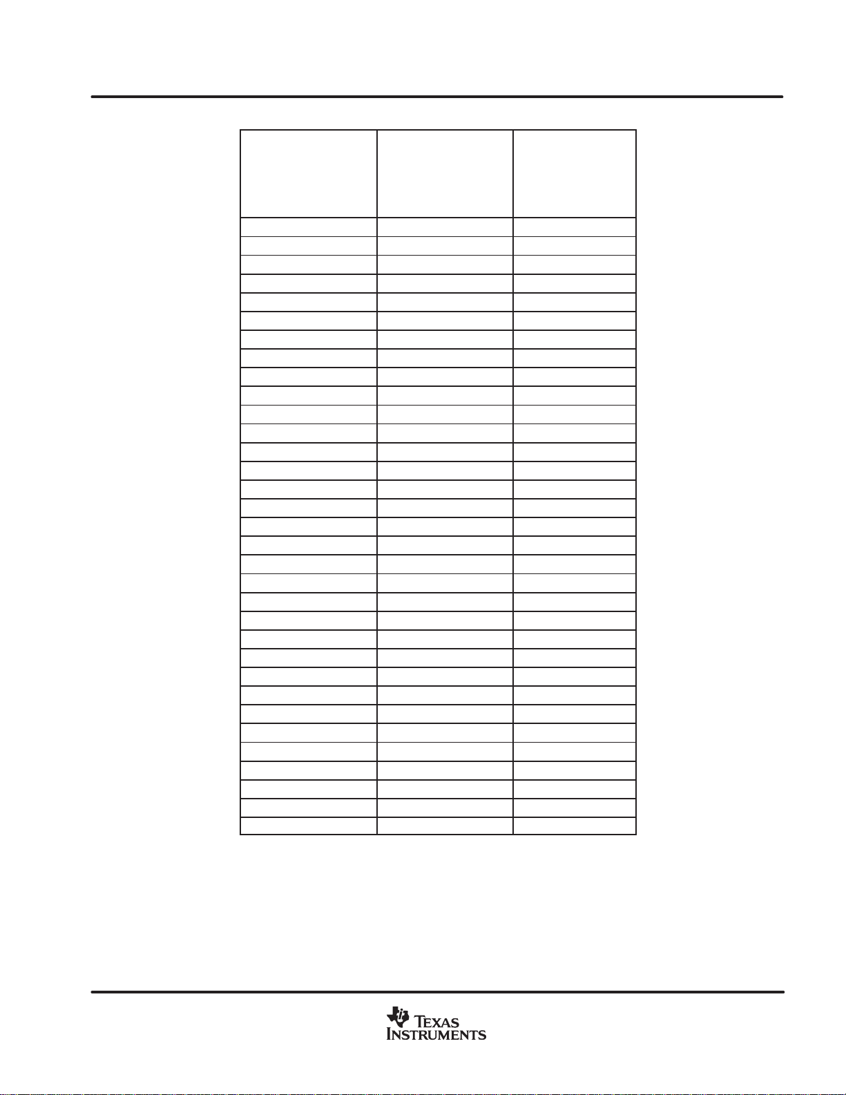
Table 1. DC Volume Control
VOLTAGE ON THE
VOLUME PIN AS A
PERCENTAGE OF
VREF (INCREASING
VOLUME OR FIXED
GAIN)
% %
0 − 4.5 0 − 2.9 −75
4.5 − 6.7 2.9 − 5.1 −40.0
6.7 − 8.91 5.1 − 7.2 −37.5
8.9 − 11.1 7.2 − 9.4 −35.0
11.1 − 13.3 9.4 − 11.6 −32.4
13.3 − 15.5 11.6 − 13.8 −29.9
15.5 − 17.7 13.8 − 16.0 −27.4
17.7 − 19.9 16.0 − 18.2 −24.8
19.9 − 22.1 18.2 − 20.4 −22.3
22.1 − 24.3 20.4 − 22.6 −19.8
24.3 − 26.5 22.6 − 24.8 −17.2
26.5 − 28.7 24.8 − 27.0 −14.7
28.7 − 30.9 27.0 − 29.1 −12.2
30.9 − 33.1 29.1 − 31.3 −9.6
33.1 − 35.3 31.3 − 33.5 −7.1
35.3 − 37.5 33.5 − 35.7 −4.6
37.5 − 39.7 35.7 − 37.9 −2.0
39.7 − 41.9 37.9 − 40.1 0.5
41.9 − 44.1 40.1 − 42.3 3.1
44.1 − 46.4 42.3 − 44.5 5.6
46.4 − 48.6 44.5 − 46.7 8.1
48.6 − 50.8 46.7 − 48.9 10.7
50.8 − 53.0 48.9 − 51.0 13.2
53.0 − 55.2 51.0 − 53.2 15.7
55.2 − 57.4 53.2 − 55.4 18.3
57.4 − 59.6 55.4 − 57.6 20.8
59.6 − 61.8 57.6 − 59.8 23.3
61.8 − 64.0 59.8 − 62.0 25.9
64.0 − 66.2 62.0 − 64.2 28.4
66.2 − 68.4 64.2 − 66.4 30.9
68.4 − 70.6 66.4 − 68.6 33.5
> 70.6 >68.6 36.0
†
Tested in production. Remaining steps are specified by design.
VOLTAGE ON THE
VOLUME PIN AS A
PERCENTAGE OF
VREF (DECREASING
VOLUME)
GAIN OF AMPLIFIER
SLOS406A − FEBRUARY 2003 − REVISED MARCH 2003
dB
†
†
†
www.ti.com
7
Page 8
O
POOutput power
SLOS406A − FEBRUARY 2003 − REVISED MARCH 2003
TYPICAL CHARACTERISTICS
Efficiency vs Output power 1
P
I
Q
I
CC
I
Q(sd)
THD+N Total harmonic distortion + noise
k
SVR
Output power
Quiescent supply current vs Supply voltage 4
Supply current vs Output Power 5
Quiescent shutdown supply current vs Supply voltage 6
Input impedance vs Gain 7
Supply ripple rejection ratio vs Frequency 12
Closed loop response 13, 14
Intermodulation performance 15
Input offset voltage vs Common-mode input voltage 16
Crosstalk vs Frequency 17
Mute attenuation
Shutdown attenuation
Common-mode rejection ratio vs Frequency 20
Table of Graphs
vs Load resistance
vs Supply voltage
vs Frequency
vs Output power
vs Frequency
FIGURE
2
3
8, 9
10, 11
18
19
8
www.ti.com
Page 9
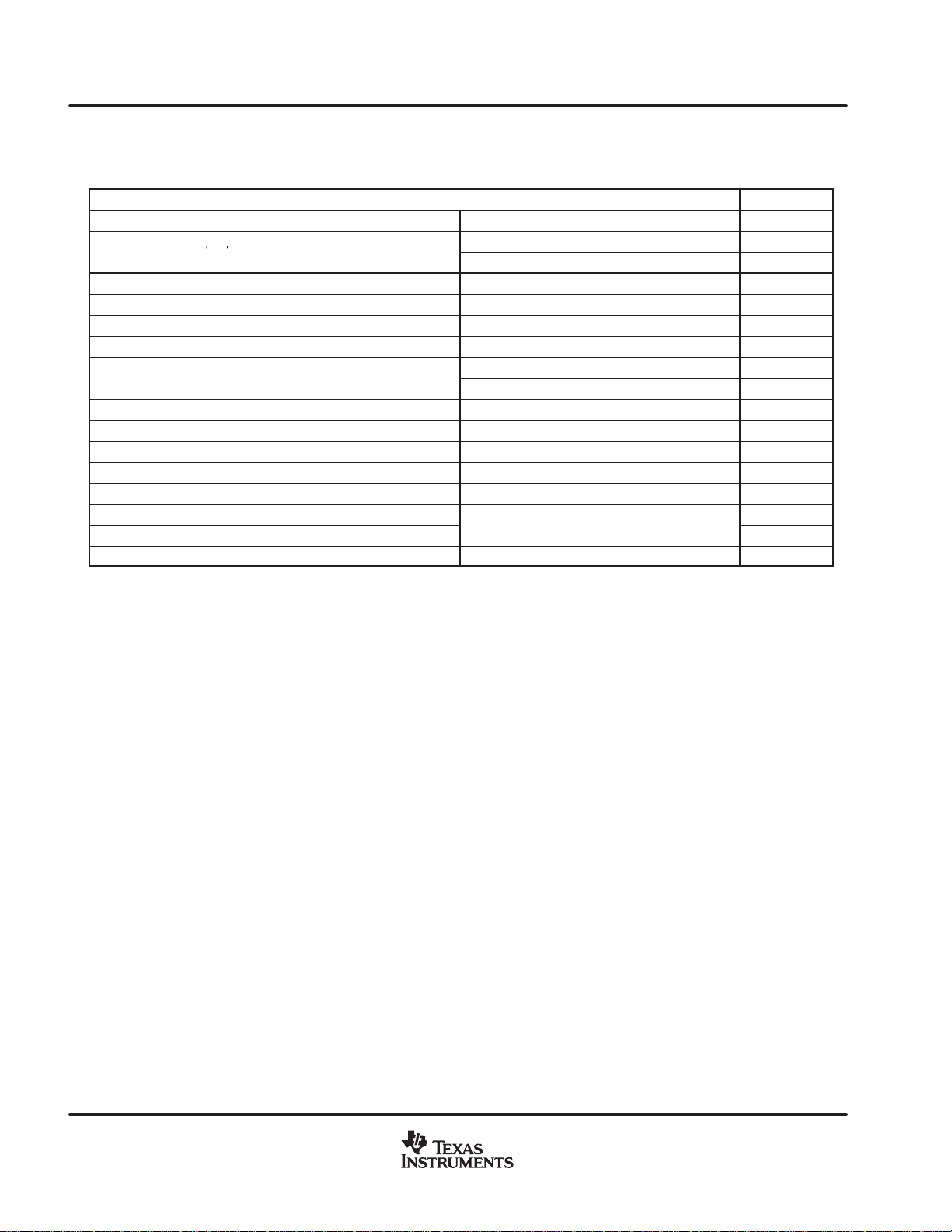
OUTPUT POWER
OUTPUT POWER
80
70
60
50
40
30
Efficiency − %
20
10
EFFICIENCY
vs
OUTPUT POWER
VCC = 12 V, RL = 8 Ω
VCC = 8.5 V, RL = 8 Ω
LC Filter
Resistive Load
SLOS406A − FEBRUARY 2003 − REVISED MARCH 2003
TYPICAL CHARACTERISTICS
8
7
6
VCC = 12 V,
THD = 10%
5
4
3
− Output Power − W
O
P
2
1
vs
LOAD RESISTANCE
Thermally Limited
VCC = 8.5 V,
THD = 10%
VCC = 12 V,
THD = 1%
VCC = 8.5 V,
THD = 1%
0
0 0.5 1 1.5 2 2.5 3
PO − Output Power − W
Figure 1
vs
SUPPLY VOLTAGE
6
5
4
3
− Output Power − W
O
P
2
1
8.5 9 10 11 12 13 14
VDD − Supply Voltage − V
Thermally Limited
8 Ω, THD = 10%
8 Ω, THD = 1%
0
8 9 10 11 12 13 14 15 16
RL − Load Resistance − Ω
Figure 2
QUIESCENT SUPPLY CURRENT
vs
SUPPLY VOLTAGE
18
17
16
15
14
13
12
Q
I − Quiescent Supply Current − mA
11
10
8.59 1011121314
TA = 25°C
VCC − Supply Voltage − V
Figure 3
www.ti.com
Figure 4
9
Page 10
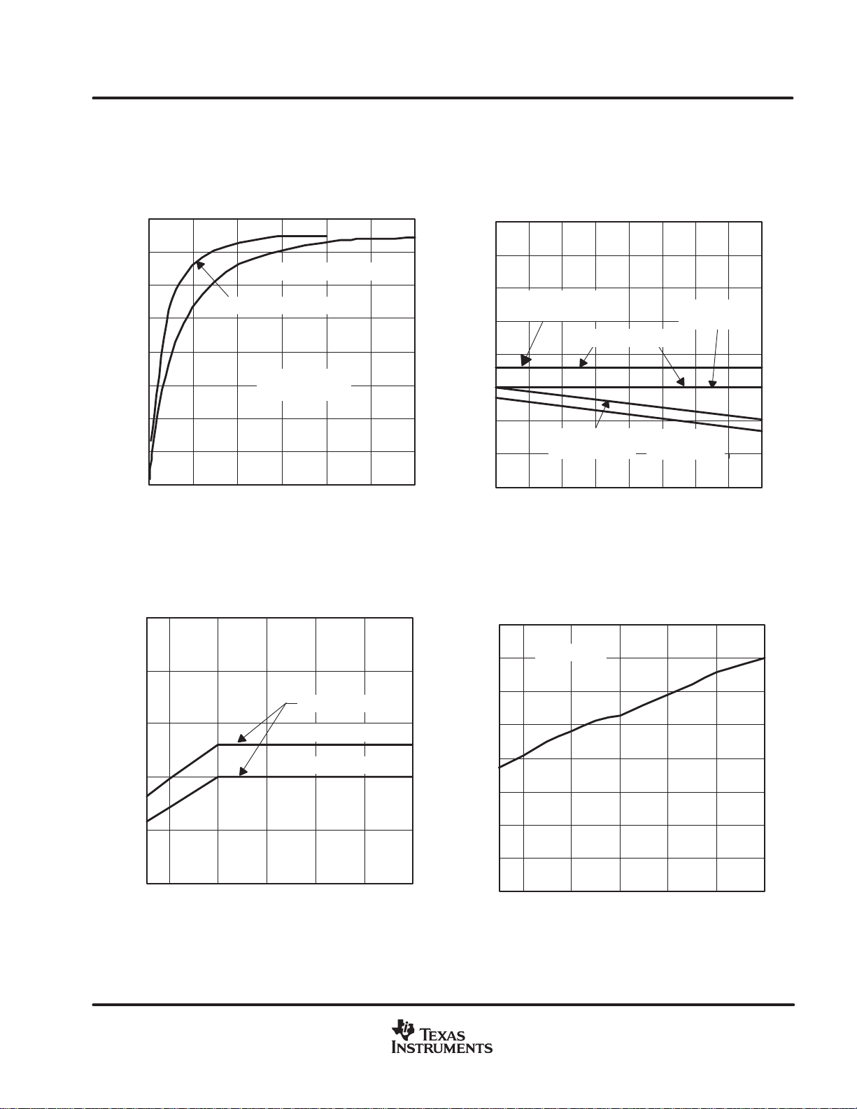
QUIESCENT SHUTDOWN SUPPLY CURRENT
SLOS406A − FEBRUARY 2003 − REVISED MARCH 2003
TYPICAL CHARACTERISTICS
SUPPLY CURRENT
vs
OUTPUT POWER (TOTAL)
0.8
VCC = 12 V,
RL = 8 Ω
0.7
0.6
0.5
vs
SUPPLY VOLTAGE
Aµ
1
0.8
0.4
− Supply Current − A
0.3
CC
I
0.2
0.1
0
0123456
PO − Output Power (Total) − W
Figure 5
INPUT IMPEDANCE
vs
GAIN
120
100
Ω
80
60
40
− Input Impedance − k
i
Z
20
0
−50 −30 −10 10
Gain − dB
30 50
0.6
0.4
0.2
− Quiescent Shutdown Supply Current −
CC
I
0
8.5 9 10 11 12 13 14
VSD = 0.8 V
VSD = 0 V
VCC − Supply Voltage − V
Figure 6
TOTAL HARMONIC DISTORTION + NOISE
vs
FREQUENCY
10
VCC = 12 V,
RL = 8 Ω,
5
TA = 25°C
2
1
0.5
PO = 1 W
0.2
0.1
0.05
0.02
THD+N − Total Harmonic Distortion + Noise − %
0.01
20 20 k50 100 200 500 1 k 2 k 5 k 10 k
PO = 3 W
f − Frequency − Hz
PO = 0.5 W
10
Figure 7
Figure 8
www.ti.com
Page 11
TOTAL HARMONIC DISTORTION + NOISE
SUPPLY RIPPLE REJECTION RATIO
TOTAL HARMONIC DISTORTION + NOISE
vs
FREQUENCY
10
VCC = 12 V,
5
RL = 8 Ω,
TA = 25°C
2
1
0.5
0.2
0.1
0.05
0.02
THD+N − Total Harmonic Distortion + Noise − %
0.01
PO = 0.5 W
20 20 k50 100 200 500 1 k 2 k 5 k 10 k
PO = 1 W
PO = 3.5 W
f − Frequency − Hz
Figure 9
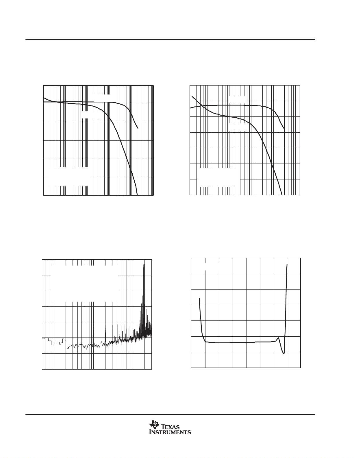
SLOS406A − FEBRUARY 2003 − REVISED MARCH 2003
TYPICAL CHARACTERISTICS
10
VCC = 8.5 V,
RL = 8 Ω,
5
TA = 25°C
2
1
0.5
0.2
0.1
0.05
0.02
THD+N − Total Harmonic Distortion + Noise − %
0.01
f = 20 KHz
20m 50m 100m 200m 500m 1 2 5 10
vs
OUTPUT POWER
f = 1 kHz
f = 20 Hz
PO − Output Power − W
Figure 10
TOTAL HARMONIC DISTORTION + NOISE
vs
OUTPUT POWER
10
VCC = 12 V,
RL = 8 Ω,
5
TA = 25°C
2
1
0.5
0.2
0.1
0.05
0.02
THD+N − Total Harmonic Distortion + Noise − %
0.01
f = 1 kHz
f = 20 Hz
f = 20 kHz
20m 50m 100m 200m 500m 1 2 5 10
PO − Output Power − W
Figure 11
vs
FREQUENCY
−40
VCC = 12 V,
−45
RL = 8 Ω
−50
−55
−60
−65
−70
−75
− Supply Ripple Rejection Ratio − dB
−80
SVR
−85
k
−90
20 100 1 k 10 k 100 k
f − Frequency − Hz
Figure 12
www.ti.com
11
Page 12
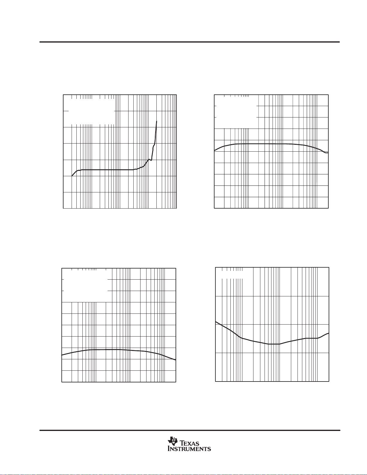
Gain − dB
Phase − Deg
FFT − dBr
− Input Offset Voltage − mV
V
SLOS406A − FEBRUARY 2003 − REVISED MARCH 2003
TYPICAL CHARACTERISTICS
CLOSED LOOP RESPONSE
50
Gain
0
Phase
−50
−100
−150
VCC = 12 V,
−200
−250
Gain = +5.6 dB,
RL = 8 Ω
10 100 1 k 10 k 100 k 1 M
f − Frequency − Hz
Figure 13
INTERMODULATION PERFORMANCE
0
−20
−40
−60
VCC = 12 V, 19 kHz, 20 kHz,
1:1, PO = 1 W, RL = 8 Ω
Gain= +13.2 dB,
BW =20 Hz to 22 kHz,
Class-D
No Filter
50
0
−50
−100
−150
−200
−250
CLOSED LOOP RESPONSE
100
50
0
−50
−100
Gain − dB
−150
VCC = 12 V,
−200
−250
Gain = +36 dB,
RL = 8 Ω
10 100 1 k 10 k 100 k 1 M
Gain
Phase
f − Frequency − Hz
Figure 14
INPUT OFFSET VOLTAGE
vs
COMMON-MODE INPUT VOLTAGE
6
VCC = 12 V
5
4
3
100
50
0
−50
Phase − Deg
−100
−150
−200
−250
12
−80
−100
−120
−140
50 100 1 k 10 k
f − Frequency − Hz
Figure 15
www.ti.com
2
1
IO
0
−1
1 1.5 2 2.5 3 3.5 4 4.5 5
V
− Common-Mode Input Voltage − V
ICM
Figure 16
Page 13
MUTE ATTENUATION
TYPICAL CHARACTERISTICS
CROSSTALK
vs
FREQUENCY
−60
VCC = 12 V,
Gain = +13.2 dB,
−65
RL = 8 Ω,
PO = 1 W
−70
−75
−80
Crosstalk − dB
−85
−90
−95
10 100 1 k 10 k 100 k
f − Frequency − Hz
Figure 17
SLOS406A − FEBRUARY 2003 − REVISED MARCH 2003
−30
VCC = 12 V,
RL = 8 Ω,
−40
VI = 1 V
−50
−60
−70
−80
−90
−100
Mute Attenuation − dB
−110
−120
−130
10 100 1 k
rms
Class-D,
VOLUME = 0 V
vs
FREQUENCY
10 k
f − Frequency − Hz
Figure 18
SHUTDOWN ATTENUATION
−80
VCC = 12 V,
RL = 8 Ω,
−85
VI = 1 V
−90
−95
−100
−105
−110
−115
Shutdown Attenuation − dB
−120
−125
−130
10 100 1 k
rms
Gain = +13.2 dB,
Class-D
vs
FREQUENCY
f − Frequency − Hz
Figure 19
10 k
COMMON-MODE REJECTION RATIO
vs
FREQUENCY
−60
VCC = 12 V
−70
−80
−90
CMRR − Common-Mode Rejection Ratio − dB
−100
20 100
f − Frequency − Hz
1 k
Figure 20
10 k 20 k
www.ti.com
13
Page 14

SLOS406A − FEBRUARY 2003 − REVISED MARCH 2003
APPLICATION INFORMATION
SHUTDOWN
RIN−
AGND
LIN−
GND
P1
50 kΩ
C2
1 µF
C3
1 µF
C1
1 µF
C5
1 µF
C4
1 µF
AGND
SD
RINN
RINP
V2P5
LINP
LINN
AVDDREF
VREF
AGND
AGND
VOLUME
REFGND
10 nF
C18
BSRN
BSLN
PVCCR
PVCCL
VCC
ROUT−
C22
1 nF
L1
(Bead)
10 µF
C15
0.1uF 0.1uF
C9
ROUTN
PVCCR
TPA3003D2
LOUTN
LOUTN
PVCCL
ROUTN
PGNDL
(Bead)
PGNDR
PGNDL
C23
1 nF
L2
PGND
C10
PGNDR
LOUTP
ROUT+
ROUTP
LOUTP
VCC
10 nF
PVCCR
ROUTP
PVCCL
C19
PVCCR
VCLAMPR
VCLAMPL
PVCCL
BSRP
MUTE
AVCC
FADE
BSLP
NC
NC
NC
AVDD
COSC
ROSC
AGND
C6
220pF
C7
1 µF
C13
0.1 µF 10 µF
C14
100 nF
R1
120 kΩ
C8
1 µF
PGND
PGND
C16
GND
VCC
AVDD
AGND
GND
MUTE
CONTROL
C11
10 nF
C20
VCC
LOUT−
C17
10 µF
L3
(Bead)
C24
1nF
PGND
(Bead)
GND GND
C12
0.1 µF0.1 µF
L4
C25
1nF
LOUT+
C21
10 nF
VCC
Figure 21. Stereo Configuration With Single-Ended Inputs
14
www.ti.com
Page 15

SLOS406A − FEBRUARY 2003 − REVISED MARCH 2003
APPLICATION INFORMATION
class-D operation
This section focuses on the class-D operation of the TPA3003D2.
traditional class-D modulation scheme
The traditional class-D modulation scheme, which is used in the TPA032D0x family, has a differential output
where each output is 180 degrees out of phase and changes from ground to the supply voltage, V
the differential prefiltered output varies between positive and negative V
, where filtered 50% duty cycle yields
CC
0 V across the load. The traditional class-D modulation scheme with voltage and current waveforms is shown
in Figure 22. Note that even at an average of 0 V across the load (50% duty cycle), the current to the load is
high, causing high loss, thus causing a high supply current.
OUTP
OUTN
+12 V
Differential Voltage
Across Load
0 V
−12 V
CC
. Therefore,
Current
Figure 22. Traditional Class-D Modulation Scheme’s Output Voltage and
Current Waveforms Into an Inductive Load With No Input
TPA3003D2 modulation scheme
The TPA3003D2 uses a modulation scheme that still has each output switching from 0 to the supply voltage.
However, OUTP and OUTN are now in phase with each other with no input. The duty cycle of OUTP is greater
than 50% and OUTN is less than 50% for positive output voltages. The duty cycle of OUTP is less than 50%
and OUTN is greater than 50% for negative output voltages. The voltage across the load sits at 0 V throughout
most of the switching period, greatly reducing the switching current, which reduces any I
2
R losses in the load.
www.ti.com
15
Page 16

SLOS406A − FEBRUARY 2003 − REVISED MARCH 2003
APPLICATION INFORMATION
TPA3003D2 modulation scheme (continued)
OUTP
OUTN
Differential
Voltage
Across
Load
+12 V
0 V
−12 V
Current
Output = 0 V
OUTP
Differential
Voltage
Across
Load
OUTN
+12 V
0 V
−12 V
Current
Output > 0 V
Figure 23. The TPA3003D2 Output Voltage and Current Waveforms Into an Inductive Load
efficiency: LC filter required with the traditional class-D modulation scheme
The main reason that the traditional class-D amplifier needs an output filter is that the switching waveform
results in maximum current flow. This causes more loss in the load, which causes lower efficiency . The ripple
current is large for the traditional modulation scheme, because the ripple current is proportional to voltage
multiplied by the time at that voltage. The differential voltage swing is 2 × V
, and the time at each voltage is
CC
half the period for the traditional modulation scheme. An ideal LC filter is needed to store the ripple current from
each half cycle for the next half cycle, while any resistance causes power dissipation. The speaker is both
resistive and reactive, whereas an LC filter is almost purely reactive.
The TP A3003D2 modulation scheme has very little loss in the load without a filter because the pulses are very
short and the change in voltage is V
instead of 2 × VCC. As the output power increases, the pulses widen,
CC
making the ripple current larger . Ripple current could be filtered with an LC filter for increased ef ficiency, but for
most applications the filter is not needed.
An LC filter with a cutoff frequency less than the class-D switching frequency allows the switching current to flow
through the filter instead of the load. The filter has less resistance than the speaker , which results in less power
dissipation, therefore increasing efficiency.
16
www.ti.com
Page 17

(1)
(2)
(3)
(4)
SLOS406A − FEBRUARY 2003 − REVISED MARCH 2003
APPLICATION INFORMATION
effects of applying a square wave into a speaker
Audio specialists have advised for years not to apply a square wave to speakers. If the amplitude of the
waveform is high enough and the frequency of the square wave is within the bandwidth of the speaker, the
square wave could cause the voice coil to jump out of the air gap and/or scar the voice coil. A 250-kHz switching
frequency, however, does not significantly move the voice coil, as the cone movement is proportional to 1/f
frequencies beyond the audio band.
Damage may occur if the voice coil cannot handle the additional heat generated from the high-frequency
switching current. The amount of power dissipated in the speaker may be estimated by first considering the
overall ef ficiency of the system. If the on-resistance (r
dominant loss in the system, then the maximum theoretical efficiency for the TPA3003D2 with an 8-Ω load is
as follows:
Efficiency (theoretical, %) + R
The maximum measured output power is approximately 3 W with an 12-V power supply. The total theoretical
power supplied (P
P
The efficiency measured in the lab using an 8-Ω speaker was 75%. The power not accounted for as dissipated
across the r
Other losses + P
+ POńEfficiency + 3Wń 0.8511 + 3.52 W
(total)
ds(on)
) for this worst-case condition would therefore be as follows:
(total)
may be calculated by simply subtracting the theoretical power from the measured power:
(measured) * P
(total)
ń
L
ǒ
RL) r
(total)
Ǔ
ds(on)
100% + 8ń(8) 1.4) 100% + 85.11%
(theoretical) + 4 * 3.52 + 0.48 W
) of the output transistors is considered to cause the
ds(on)
2
for
The quiescent supply current at 12 V is measured to be 28.5 mA. It can be assumed that the quiescent current
encapsulates all remaining losses in the device, i.e., biasing and switching losses. It may be assumed that any
remaining power is dissipated in the speaker and is calculated as follows:
P
+ 0.48 W * (12 V 28.5 mA) + 0.14 W
(dis)
Note that these calculations are for the worst-case condition of 3 W delivered to the speaker. Since the 0.14 W
is only 5% of the power delivered to the speaker, it may be concluded that the amount of power actually
dissipated in the speaker is relatively insignificant. Furthermore, this power dissipated is well within the
specifications of most loudspeaker drivers in a system, as the power rating is typically selected to handle the
power generated from a clipping waveform.
when to use an output filter
Design the TPA3003D2 without the filter if the traces from amplifier to speaker are short (< 1 inch). Powered
speakers, where the speaker is in the same enclosure as the amplifier , is a typical application for class-D without
a filter.
Most applications require a ferrite bead filter. The ferrite filter reduces EMI around 1 MHz and higher (FCC and
CE only test radiated emissions greater than 30 MHz). When selecting a ferrite bead, choose one with high
impedance at high frequencies, but very low impedance at low frequencies.
Use a LC output filter if there are low frequency (<1 MHz) EMI sensitive circuits and/or there are long wires from
the amplifier to the speaker.
www.ti.com
17
Page 18

SLOS406A − FEBRUARY 2003 − REVISED MARCH 2003
APPLICATION INFORMATION
when to use an output filter (continued)
OUTP
OUTN
Figure 24. Typical LC Output Filter, Cutoff Frequency of 41 kHz, Speaker Impedance = 8 Ω
OUTP
33 µH
L
1
33 µH
L
2
Ferrite
Chip Bead
C
1
0.47 µF
C
2
0.1 µF
C
3
0.1 µF
Ferrite
Chip Bead
OUTN
1 nF
1 nF
Figure 25. Typical Ferrite Chip Bead Filter (Chip bead example: Fair-Rite 2512067007Y3)
volume control operation
The VOLUME terminal controls the internal amplifier gain. This pin is controlled with a dc voltage, which should
not exceed VREF. Table 1 lists the gain as determined by the voltage on the VOLUME pin in reference to the
voltage on VREF.
If using a resistor divider to fix the gain of the amplifier, the VREF terminal can be directly connected to
AVDDREF and a resistor divider can be connected across VREF and REFGND. (See Figure 21 in the
Application Information Section). For fixed gain, calculate the resistor divider values necessary to center the
voltage between the two percentage points given in the first column of Table 1. For example, if a gain of 10.7
dB is desired, the resistors in the divider network can both be 10 kΩ. With these resistor values, a voltage of
50%*VREF will be present at the VOLUME pin and result in a class-D gain of 10.7 dB.
If using a DAC to control the class-D gain, VREF and REFGND should be connected to the reference voltage
for the DAC and the GND terminal of the DAC, respectively. For the DAC application, AVDDREF would be left
unconnected. The reference voltage of the DAC provides the reference to the internal gain circuitry through the
VREF input and any fluctuations in the DAC output voltage will not affect the TPA3003D2 gain. The percentages
in the first column of T able 1 should be used for setting the voltages of the DAC when the voltage on the VOLUME
terminal is increased. The percentages in the second column should be used for the DAC voltages when
decreasing the voltage on the VOLUME terminal. Two lookup tables should be used in software to control the
gain based on an increase or decrease in the desired system volume. This is explained further in a section
below.
18
www.ti.com
Page 19

SLOS406A − FEBRUARY 2003 − REVISED MARCH 2003
APPLICATION INFORMATION
volume control operation (continued)
If using an analog potentiometer to control the gain, it should be connected between VREF and REFGND.
VREF can be connected to AVDDREF or an external voltage source, if desired. The first and second column
in Table 1 should be used to determine the point at which the gain changes depending on the direction that the
potentiometer is turned. If the voltage on the center tap of the potentiometer is increasing, the first column in
Table 1 should be referenced to determine the trip points. If the voltage is decreasing, the trip points in the
second column should be referenced.
The trip point, where the gain actually changes, is different depending on whether the voltage on the VOLUME
terminal is increasing or decreasing as a result of hysteresis about each trip point. The hysteresis ensures that
the gain control is monotonic and does not oscillate from one gain step to another. A pictorial representation
of the volume control can be found in Figure 26. The graph focuses on three gain steps with the trip points
defined in the first and second columns of Table 1. The dotted lines represent the hysteresis about each gain
step.
The timing of the volume control circuitry is controlled by an internal 60-Hz clock. This clock determines the
rate at which the gain changes when adjusting the voltage on the external volume control pins. The gain updates
every 4 clock cycles (nominally 67 ms based on a 60 Hz clock) to the next step until the final desired gain is
reached. For example, if the TP A3003D2 is currently in the +0.53 dB gain step and the VOLUME pin is adjusted
for maximum gain at +36 dB, the time required for the gain to reach +36 dB is 14 steps x 67ms/step = 0.938
seconds. Referencing Table 1, there are 14 steps between the +0.53 dB gain step and the maximum gain step
of +36 dB.
Decreasing Voltage on
VOLUME Terminal
5.6
3.1
Increasing Voltage on
Class-D Gain − dB
0.5
(40.1%*VREF)
2.00
2.10
(41.9%*VREF)
Voltage on VOLUME Pin − V
2.11
(42.3%*VREF)
VOLUME Terminal
2.21
(44.1%*VREF)
Figure 26. DC Volume Control Operation, VREF = 5 V
www.ti.com
19
Page 20
SLOS406A − FEBRUARY 2003 − REVISED MARCH 2003
APPLICATION INFORMATION
FADE
operation
The FADE terminal is a logic input that controls the operation of the volume control circuitry during transitions
to and from the shutdown state and during power-up.
A logic low on this terminal places the amplifier in the fade mode. During power-up or recovery from the
shutdown state (a logic high is applied to the SD terminal), the volume is smoothly ramped up from the mute
state, −75 dB, to the desired volume setting determined by the voltage on the volume control terminal.
Conversely, the volume is smoothly ramped down from the current state to the mute state when a logic low is
applied to the SD
This clock determines the rate at which the gain changes when adjusting the voltage on the external volume
control pins. The gain updates every 4 clock cycles (nominally 67 ms based on a 60 Hz clock) to the next step
until the final desired gain is reached. For example, if the TP A3003D2 is currently in the +0.53 dB class-D gain
step and the VOLUME pin is adjusted for maximum gain at +36 dB, the time required for the gain to reach 36
dB is 14 steps x 67 ms/step = 0.938 seconds. Referencing Table 1, there are 14 steps between the +0.53 dB
gain step and the maximum gain step of +36 dB.
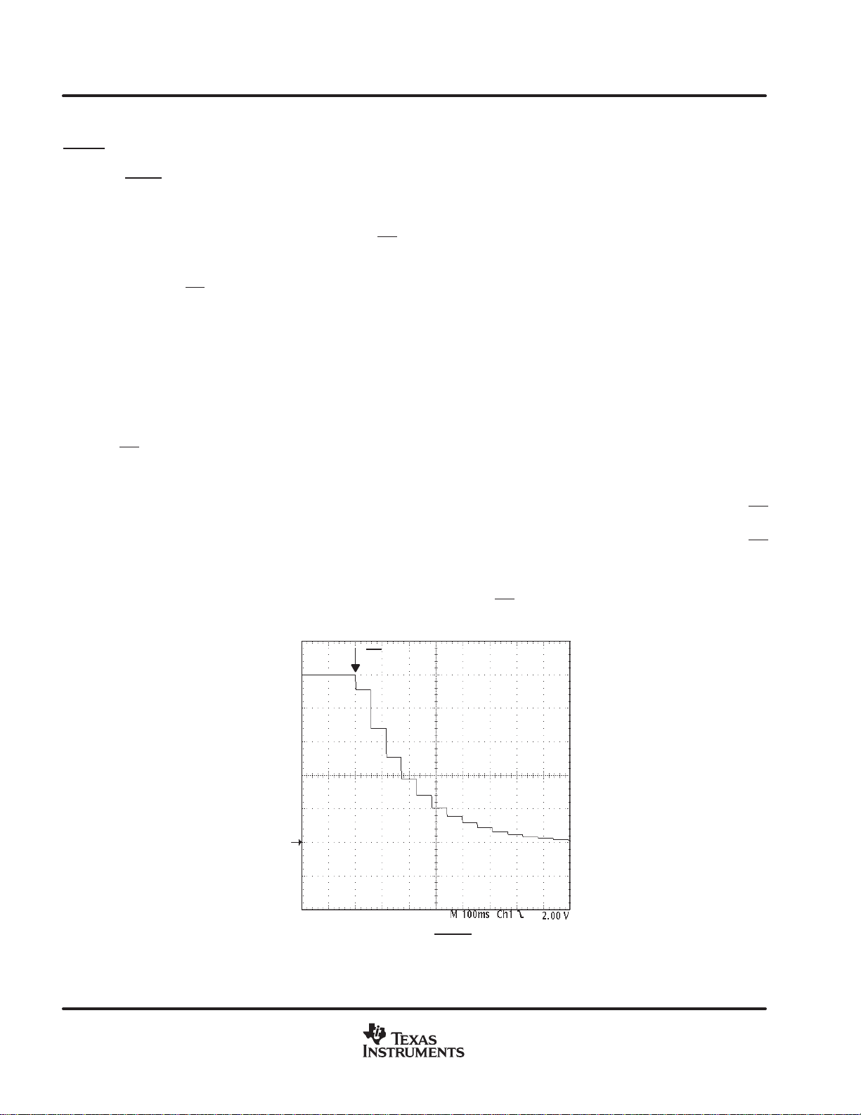
Figure 27 shows a scope capture of the differential output (measured across OUT+ and OUT−) with the amplifier
in the fade mode. A 1 V
the SD
terminal at the time defined in the figure. The figure depicts the outputs transitioning from one gain step
to the next lower step at approximately 67 ms/step.
terminal. The timing of the volume control circuitry is controlled by an internal 60-Hz clock.
dc voltage was applied across the differential inputs and a logic low was applied to
pp
A logic high on this pin disables the volume fade effect during transitions to and from the shutdown state and
during power-up. During power-up or recovery from the shutdown state (a logic high is applied to the SD
terminal), the transition from the mute state, −75 dB, to the desired volume setting is less than 1 ms. Conversely,
the volume ramps down from current state to the mute state within 1 ms when a logic low is applied to the SD
terminal.
Figure 28 shows a scope capture of the differential output with the fade effect disabled. The outputs transition
to the lowest gain state within 1ms of applying a logic low to the SD
SD = 0V
GND
terminal.
20
Figure 27. Differential Output With FADE (Terminal 30) Held Low
www.ti.com
Page 21

SLOS406A − FEBRUARY 2003 − REVISED MARCH 2003
APPLICATION INFORMATION
SD
= 0 V
GND
Figure 28. Differential Output With FADE Terminal Held High
MUTE operation
The MUTE pin is an input for controlling the output state of the TPA3003D2. A logic high on this pin disables
the outputs. A logic low on this pin enables the outputs. This pin may be used as a quick disable or enable of
the outputs without a volume fade. Quiescent current is listed in the dc characteristics specification table. The
MUTE pin should never be left floating.
For power conservation, the SD
pin should be used to reduce the quiescent current to the absolute minimum
level. The volume will fade, slowly increase or decrease, when leaving or entering the shutdown state if the
FADE
terminal is held low. If the FADE terminal is held high, the outputs will transition very quickly. Refer to the
FADE
operation section.
SD operation
The TPA3003D2 employs a shutdown mode of operation designed to reduce supply current (ICC) to the absolute
minimum level during periods of nonuse for power conservation. The SD
specification table for trip point)during normal operation when the amplifier is in use. Pulling SD
outputs to mute and the amplifier to enter a low-current state. SD
input terminal should be held high (see
low causes the
should never be left unconnected, because
amplifier operation would be unpredictable.
For the best power-off pop performance, the amplifier should be placed in the shutdown mode prior to removing
the power supply voltage.
selection of COSC and ROSC
The switching frequency is determined using the values of the components connected to ROSC (pin 20) and
COSC (pin 21) and may be calculated with the following equation:
f
OSC
= 6.6 / (R
OSC
* C
OSC
)
The frequency may be varied from 225 kHz to 275 kHz by adjusting the values chosen for R
The recommended values are C
= 220 pF, R
OSC
=120 kΩ for a switching frequency of 250 kHz.
OSC
www.ti.com
OSC
and C
OSC
.
21
Page 22

(5)
SLOS406A − FEBRUARY 2003 − REVISED MARCH 2003
APPLICATION INFORMATION
internal 2.5-V bias generator capacitor selection
The internal 2.5-V bias generator (V2P5) provides the internal bias for the preamplifier stage. The external input
capacitors and this internal reference allow the inputs to be biased within the optimal common-mode range of
the input preamplifiers.
The selection of the capacitor value on the V2P5 terminal is critical for achieving the best device performance.
During startup or recovery from the shutdown state, the V2P5 capacitor determines the rate at which the
amplifier starts up. When the voltage on the V2P5 capacitor equals 0.75 x V2P5, or 75% of its final value, the
device turns on and the class-D outputs start switching. The startup time is not critical for the best depop
performance since any pop sound that is heard is the result of the class-D outputs switching on and not the
startup time. However, at least a 0.47-µF capacitor is recommended for the V2P5 capacitor.
A secondary function of the V2P5 capacitor is to filter high frequency noise on the internal 2.5-V bias generator.
input resistance
Each gain setting is achieved by varying the input resistance of the amplifier, which can range from its smallest
value to over six times that value. As a result, if a single capacitor is used in the input high-pass filter, the −3 dB
or cutoff frequency also changes by over six times.
C
Input
Signal
i
IN
Z
i
The −3-dB frequency can be calculated using equation 5.
+
1
2p ZiC
i
i
) is required to allow the amplifier to bias the input signal to the
i
f
*3dB
input capacitor, C
In the typical application an input capacitor (C
proper dc level (V2P5) for optimum operation. In this case, C
a high-pass filter with the corner frequency determined in equation 6.
−3 dB
+
2p Z
1
C
i
i
f
c
Z
f
and the input impedance of the amplifier (Zi) form
i
(6)
22
www.ti.com
f
c
Page 23

(7)
SLOS406A − FEBRUARY 2003 − REVISED MARCH 2003
APPLICATION INFORMATION
The value of Ci is important, as it directly affects the bass (low frequency) performance of the circuit. Consider
the example where Z
is reconfigured as equation 7.
C
+
i
2p Z
In this example, Ci is 0.4 µF, so one would likely choose a value in the range of 0.47 µF to 1 µF. If the gain is
known and will be constant, use Z
lowest gain step intended for use in the system. A further consideration for this capacitor is the leakage path
from the input source through the input network (C
creates a dc offset voltage at the input to the amplifier that reduces useful headroom, especially in high gain
applications. For this reason a low-leakage tantalum or ceramic capacitor is the best choice. When polarized
capacitors are used, the positive side of the capacitor should face the amplifier input in most applications as
the dc level there is held at 2.5 V, which is likely higher than the source dc level. Note that it is important to confirm
the capacitor polarity in the application.
power supply decoupling, C
The TPA3003D2 is a high-performance CMOS audio amplifier that requires adequate power supply decoupling
to ensure the output total harmonic distortion (THD) is as low as possible. Power supply decoupling also
prevents oscillations for long lead lengths between the amplifier and the speaker. The optimum decoupling is
achieved by using two capacitors of different types that target dif ferent types of noise on the power supply leads.
For higher frequency transients, spikes, or digital hash on the line, a good low equivalent-series-resistance
(ESR) ceramic capacitor, typically 0.1 µF placed as close as possible to the device V
filtering lower-frequency noise signals, a larger aluminum electrolytic capacitor of 10 µF or greater placed near
the audio power amplifier is recommended. The 10-µF capacitor also serves as a local storage capacitor for
supplying current during large signal transients on the amplifier outputs.
is 20 kΩ and the specification calls for a flat bass response down to 20 Hz. Equation 6
i
1
f
c
i
to calculate Ci. Calculations for Ci should be based off the impedance at the
i
) and the feedback network to the load. This leakage current
i
S
lead works best. For
CC
BSN and BSP capacitors
The full H-bridge output stages use only NMOS transistors. They therefore require bootstrap capacitors for the
high side of each output to turn on correctly. A 10-nF ceramic capacitor, rated for at least 25 V, must be connected
from each output to its corresponding bootstrap input. Specifically, one 10-nF capacitor must be connected from
xOUTP to xBSP, and one 10-nF capacitor must be connected from xOUTN to xBSN. (See the application circuit
diagram in Figure 21.)
VCLAMP capacitors
To ensure that the maximum gate-to-source voltage for the NMOS output transistors is not exceeded, two
internal regulators clamp the gate voltage. Two 1-µF capacitors must be connected from VCLAMPL (pin 25)
and VCLAMPR (pin 36) to ground and must be rated for at least 25 V. The voltages at the VCLAMP terminals
vary with V
internal regulated 5-V supply (AV
The AV
and may not be used for powering any other circuitry.
CC
)
DD
terminal (pin 29) is the output of an internally-generated 5-V supply, used for the oscillator,
DD
preamplifier, and volume control circuitry. It requires a 0.1-µF to 1-µF capacitor, placed very close to the pin,
to ground to keep the regulator stable. The regulator may not be used to power any external circuitry.
www.ti.com
23
Page 24

(8)
(9)
SLOS406A − FEBRUARY 2003 − REVISED MARCH 2003
APPLICATION INFORMATION
differential input
The differential input stage of the amplifier cancels any noise that appears on both input lines of the channel.
To use the TPA3003D2 with a differential source, connect the positive lead of the audio source to the INP input
and the negative lead from the audio source to the INN input. To use the TPA3003D2 with a single-ended source,
ac ground the INP input through a capacitor equal in value to the input capacitor on INN and apply the audio
source to the INN input. In a single-ended input application, the INP input should be ac-grounded at the audio
source instead of at the device input for best noise performance.
using low-ESR capacitors
Low-ESR capacitors are recommended throughout this application section. A real (as opposed to ideal)
capacitor can be modeled simply as a resistor in series with an ideal capacitor. The voltage drop across this
resistor minimizes the beneficial effects of the capacitor in the circuit. The lower the equivalent value of this
resistance the more the real capacitor behaves like an ideal capacitor.
short-circuit protection
The TPA3003D2 has short circuit protection circuitry on the outputs that prevents damage to the device during
output-to-output shorts, output-to-GND shorts, and output-to-V
the outputs, the output drive is immediately disabled. This is a latched fault and must be reset by cycling the
voltage on the SD
pin to a logic low and back to the logic high state for normal operation. This will clear the
short-circuit flag and allow for normal operation if the short was removed. If the short was not removed, the
protection circuitry will again activate.
shorts. When a short-circuit is detected on
CC
thermal protection
Thermal protection on the TPA3003D2 prevents damage to the device when the internal die temperature
exceeds 150°C. There is a ±15 degree tolerance on this trip point from device to device. Once the die
temperature exceeds the thermal set point, the device enters into the shutdown state and the outputs are
disabled. This is not a latched fault. The thermal fault is cleared once the temperature of the die is reduced by
20°C. The device begins normal operation at this point with no external system interaction.
thermal considerations: output power and maximum ambient temperature
To calculate the maximum ambient temperature, the following equation may be used:
T
= TJ – ΘJAP
Amax
where: T
Θ
JA
= 150°C
J
= 45°C/W
(The derating factor for the 48-pin PFB package is given in the dissipation rating table.)
To estimate the power dissipation, the following equation may be used:
P
Dissipated
= P
Efficiency = ~75% for an 8-Ω load
Dissipated
O(average)
x ((1 / Efficiency) – 1)
24
www.ti.com
Page 25

SLOS406A − FEBRUARY 2003 − REVISED MARCH 2003
APPLICATION INFORMATION
thermal considerations: output power and maximum ambient temperature (continued)
Example. What is the maximum ambient temperature for an application that requires the TP A3003D2 to drive
3 W into an 8-Ω speaker (stereo)?
P
Dissipated
T
Amax
This calculation shows that the TPA3003D2 can drive 3 W of continuous RMS power per channel into an 8-Ω
speaker up to an ambient temperature of 60°C.
printed circuit board (PCB) layout
Because the TPA3003D2 is a class-D amplifier that switches at a high frequency, the layout of the printed circuit
board (PCB) should be optimized according to the following guidelines for the best possible performance.
D Decoupling capacitors — As described on page 23, the high-frequency 0.1-uF decoupling capacitors
should be placed as close to the PVCC (pin 14, 15, 22, 23, 38, 39, 46, 47) and A V
possible. The V2P5 (pin 4) capacitor , AV
also be placed as close to the device as possible. Large (10 uF or greater) bulk power supply decoupling
capacitors should be placed near the TPA3003D2 on the PVCCL, PVCCR, and AV
D Grounding — The AV
COSC (pin 28) capacitor, and ROSC (pin 27) resistor should each be grounded to analog ground (AGND,
pin 26. The PVCC (pin 9 and pin 16) decoupling capacitors should each be grounded to power ground
(PGND, pins 18, 19, 42, 43). Basically, an AGND island should be created with a single connection to PGND.
= 6 W x ((1 / 0.75) – 1) = 2 W (PO = 3 W * 2)
= 150°C – (45°C/W x 2 W) = 60°C
(pin 29) capacitor, and VCLAMP (pins 25, 36) capacitor should
DD
(pin 33) decoupling capacitor, AVDD (pin 29) capacitor, V2P5 (pin 4) capacitor,
CC
(pin 33) terminals as
CC
terminals.
CC
D Output filter — The ferrite EMI filter (Figure 25, page 18) should be placed as close to the output terminals
as possible for the best EMI performance. The LC filter (Figure 24, page 18 should be placed close to the
outputs. The capacitors used in both the ferrite and LC filters should be grounded to PGND.
For an example layout, please refer to the TPA3003D2 Evaluation Module (TPA3003D2EVM) User Manual, TI
literature number SLOU159. The EVM user manual is available on the TI web site at http://www.ti.com.
basic measurement system
This section focuses on methods that use the basic equipment listed below:
D Audio analyzer or spectrum analyzer
D Digital multimeter (DMM)
D Oscilloscope
D Twisted pair wires
D Signal generator
D Power resistor(s)
D Linear regulated power supply
D Filter components
D EVM or other complete audio circuit
www.ti.com
25
Page 26

SLOS406A − FEBRUARY 2003 − REVISED MARCH 2003
APPLICATION INFORMATION
Figure 29 shows the block diagrams of basic measurement systems for class-AB and class-D amplifiers. A sine
wave is normally used as the input signal since it consists of the fundamental frequency only (no other harmonics
are present). An analyzer is then connected to the APA output to measure the voltage output. The analyzer must
be capable of measuring the entire audio bandwidth. A regulated dc power supply is used to reduce the noise
and distortion injected into the APA through the power pins. A System Two audio measurement system (AP-II)
(Reference 1) by Audio Precision includes the signal generator and analyzer in one package.
The generator output and amplifier input must be ac-coupled. However, the EVMs already have the ac-coupling
capacitors, (C
attenuating the test signal, and is important since the input resistance of AP As is not very high (about 10 kΩ).
Conversely the analyzer-input impedance should be high. The output impedance, R
in the hundreds of milliohms and can be ignored for all but the power-related calculations.
Figure 29(a) shows a class-AB amplifier system, which is relatively simple because these amplifiers are linear
their output signal is a linear representation of the input signal. They take analog signal input and produce analog
signal output. These amplifier circuits can be directly connected to the AP-II or other analyzer input.
This is not true of the class-D amplifier system shown in Figure 29(b), which requires low pass filters in most
cases in order to measure the audio output waveforms. This is because it takes an analog input signal and
converts it into a pulse-width modulated (PWM) output signal that is not accurately processed by some
analyzers.
), so no additional coupling is required. The generator output impedance should be low to avoid
IN
, of the AP A is normally
OUT
26
www.ti.com
Page 27

Signal
Generator
Signal
Generator
Power Supply
Class−D APA
SLOS406A − FEBRUARY 2003 − REVISED MARCH 2003
APPLICATION INFORMATION
Power Supply
APA
(a) Basic Class−AB
Low−Pass RC
R
L
Low−Pass RC
R
L
Filter
Filter
Analyzer
20 Hz − 20 kHz
Analyzer
20 Hz − 20 kHz
(b) Filter−Free and Traditional Class−D
Figure 29. Audio Measurement Systems
The TPA3003D2 uses a modulation scheme that does not require an output filter for operation, but they do
sometimes require an RC low-pass filter when making measurements. This is because some analyzer inputs
cannot accurately process the rapidly changing square-wave output and therefore record an extremely high
level of distortion. The RC low-pass measurement filter is used to remove the modulated waveforms so the
analyzer can measure the output sine wave.
www.ti.com
27
Page 28
SLOS406A − FEBRUARY 2003 − REVISED MARCH 2003
APPLICATION INFORMATION
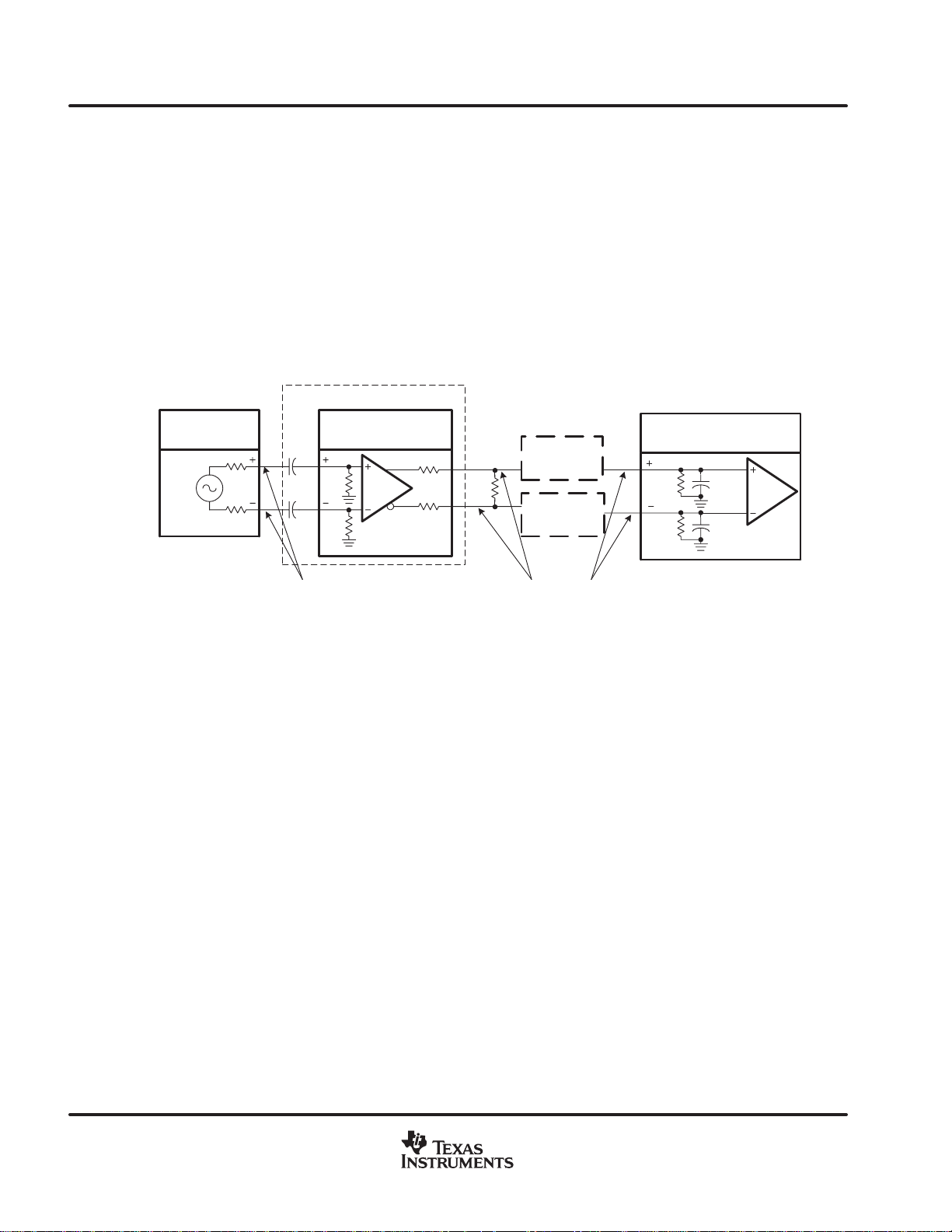
differential input and BTL output
All of the class-D APAs and many class-AB APAs have differential inputs and bridge-tied load (BTL) outputs.
Differential inputs have two input pins per channel and amplify the difference in voltage between the pins.
Differential inputs reduce the common-mode noise and distortion of the input circuit. BTL is a term commonly
used in audio to describe differential outputs. BTL outputs have two output pins providing voltages that are 180
degrees out of phase. The load is connected between these pins. This has the added benefits of quadrupling
the output power to the load and eliminating a dc blocking capacitor.
A block diagram of the measurement circuit is shown in Figure 30. The differential input is a balanced input,
meaning the positive (+) and negative (−) pins will have the same impedance to ground. Similarly, the BTL output
equates to a balanced output.
Evaluation Module
IN
IN
Audio Power
Amplifier
R
IN
R
IN
Analyzer
Low−Pass
RC Filter
R
OUT
R
OUT
R
L
Low−Pass
RC Filter
R
ANA
R
ANA
C
ANA
C
ANA
Generator
V
GEN
C
R
GEN
R
GEN
C
Twisted−Pair Wire
Twisted−Pair Wire
Figure 30. Differential Input—BTL Output Measurement Circuit
The generator should have balanced outputs and the signal should be balanced for best results. An unbalanced
output can be used, but it may create a ground loop that will affect the measurement accuracy. The analyzer
must also have balanced inputs for the system to be fully balanced, thereby cancelling out any common mode
noise in the circuit and providing the most accurate measurement.
The following general rules should be followed when connecting to APAs with differential inputs and BTL
outputs:
D Use a balanced source to supply the input signal.
D Use an analyzer with balanced inputs.
D Use twisted-pair wire for all connections.
D Use shielding when the system environment is noisy.
D Ensure the cables from the power supply to the APA, and from the APA to the load, can handle the large
currents (see Table 2).
Table 2 shows the recommended wire size for the power supply and load cables of the APA system. The real
concern is the dc or ac power loss that occurs as the current flows through the cable. These recommendations
are based on 12-inch long wire with a 20-kHz sine-wave signal at 25°C.
28
www.ti.com
Page 29
SLOS406A − FEBRUARY 2003 − REVISED MARCH 2003
APPLICATION INFORMATION
Table 2. Recommended Minimum Wire Size for Power Cables
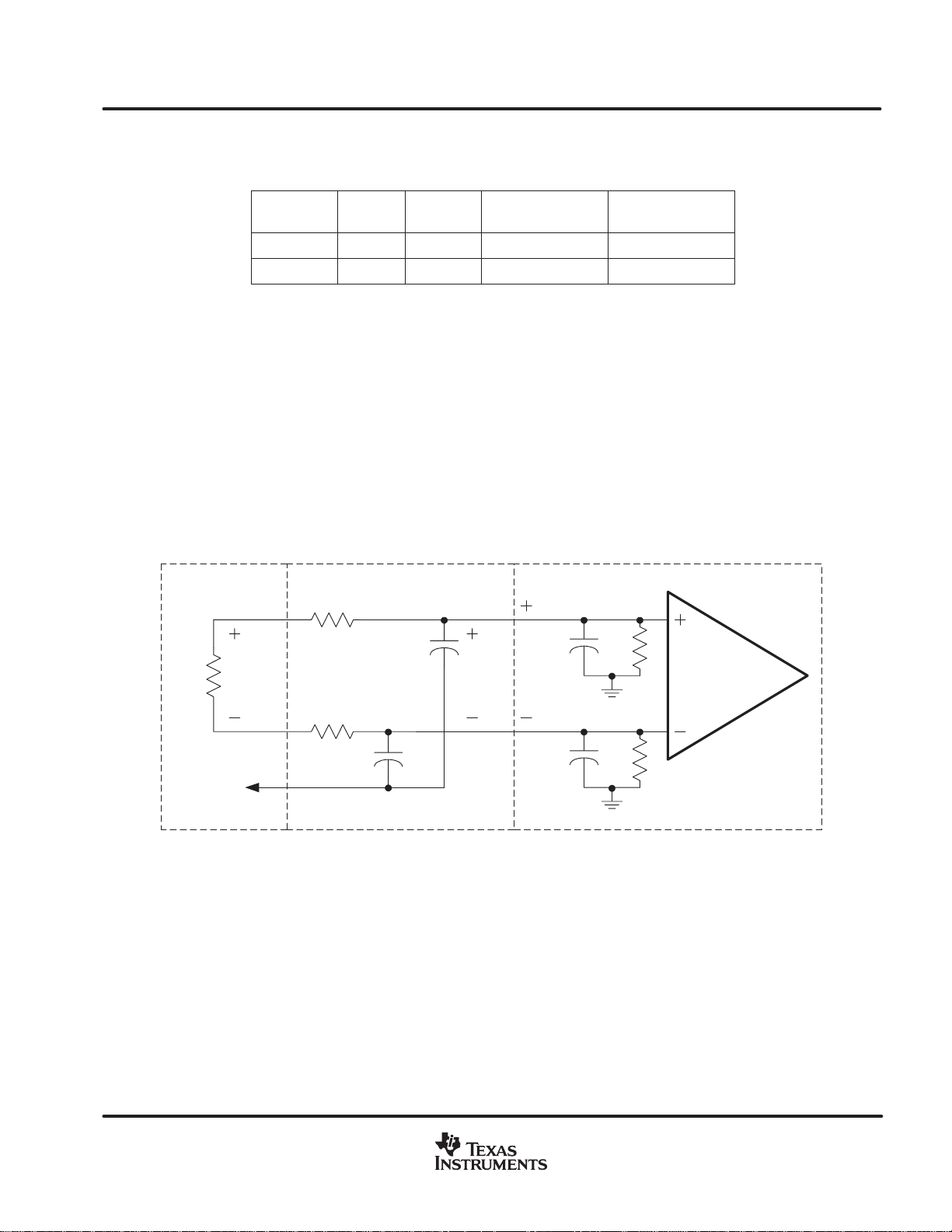
P
OUT
(W)
1 8 22 to 28 2.0 8.0 2.1 8.1
< 0.75 8 22 to 28 1.5 6.1 1.6 6.2
Class-D RC low-pass filter
A RC filter is used to reduce the square-wave output when the analyzer inputs cannot process the pulse-width
modulated class-D output waveform. This filter has little effect on the measurement accuracy because the cutoff
frequency is set above the audio band. The high frequency of the square wave has negligible impact on
measurement accuracy because it is well above the audible frequency range and the speaker cone cannot
respond at such a fast rate. The RC filter is not required when an LC low-pass filter is used, such as with the
class-D APAs that employ the traditional modulation scheme (TPA032D0x, TPA005Dxx).
The component values of the RC filter are selected using the equivalent output circuit as shown in Figure 31.
R
is the load impedance that the AP A is driving for the test. The analyzer input impedance specifications should
L
be available and substituted for R
for the system. The filter should be grounded to the APA near the output ground pins or at the power supply
ground pin to minimize ground loops.
R
L
(Ω)
ANA
AWG SIZE DC POWER LOSS
and C
. The filter components, R
ANA
(mW)
AC POWER LOSS
(mW)
and C
FILT
, can then be derived
FILT
Load
R
FILT
C
FILT
VL= V
R
L
IN
R
FILT
C
FILT
V
OUT
C
ANA
C
ANA
AP Analyzer InputRC Low−Pass Filters
R
ANA
R
ANA
T o AP A
GND
Figure 31. Measurement Low-Pass Filter Derivation Circuit—Class-D APAs
www.ti.com
29
Page 30
(10)
(11)
(12)
SLOS406A − FEBRUARY 2003 − REVISED MARCH 2003
APPLICATION INFORMATION
The transfer function for this circuit is shown in equation (10) where ω
= (C
bandwidth, to avoid attenuating the audio signal. Equation (11) provides this cutoff frequency, f
R
minimize the attenuation of the analyzer-input voltage through the voltage divider formed by R
A rule of thumb is that R
error to less than 1% for R
ǒ
fC+ 2Ǹ f
An exception occurs with the efficiency measurements, where R
reduce the current shunted through the filter. C
cutoff frequency. See Table 3 for the recommended filter component values.
Once f
calculated value is not available, it is better to choose a smaller capacitance value to keep f
desired value calculated in equation (11).
C
+ C
FILT
must be chosen large enough to minimize current that is shunted from the load, yet small enough to
FILT
V
OUT
Ǔ
V
IN
is determined and R
C
+
FILT
). The filter frequency should be set above f
ANA
should be small (~100 Ω) for most measurements. This reduces the measurement
R
ǒ
+
MAX
2p fC R
ANA
R
ANA)RFILT
1 ) j
1
FILT
ǒ
ANA
w
w
O
FILT
≥ 10 kΩ.
Ǔ
Ǔ
is selected, the filter capacitance is calculated using equation (12). When the
FILT
MAX
must be decreased by a factor of ten to maintain the same
FILT
= REQCEQ, REQ = R
O
, the highest frequency of the measurement
must be increased by a factor of ten to
FILT
R
FILT
C
ANA
. The value of
C
FILT
above the minimum
and C
and R
EQ
ANA
.
Table 3 shows recommended values of R
was originally calculated to be 28 kHz for an f
but the nearest values of 56000 pF and 51000 pF were not available. A 47000 pF capacitor was used instead,
and f
is 34 kHz, which is above the desired value of 28 kHz.
C
Table 3. Typical RC Measurement Filter Values
MEASUREMENT R
Efficiency 1 000 Ω 5 600 pF
All other measurements 100 Ω 56 000 pF
FILT
and C
of 20 kHz. C
MAX
based on common component values. The value of f
FILT
FILT
, however, was calculated to be 57000 pF,
FILT
C
FILT
C
30
www.ti.com
Page 31
PACKAGE OPTION ADDENDUM
www.ti.com
18-Apr-2006
PACKAGING INFORMATION
Orderable Device Status
(1)
Package
Type
Package
Drawing
Pins Package
Qty
Eco Plan
TPA3003D2PFB ACTIVE TQFP PFB 48 250 Green (RoHS &
no Sb/Br)
TPA3003D2PFBG4 ACTIVE TQFP PFB 48 250 Green (RoHS &
no Sb/Br)
TPA3003D2PFBR ACTIVE TQFP PFB 48 1000 Green (RoHS &
no Sb/Br)
TPA3003D2PFBRG4 ACTIVE TQFP PFB 48 1000 Green (RoHS &
no Sb/Br)
(1)
The marketing status values are defined as follows:
ACTIVE: Product device recommended for new designs.
LIFEBUY: TI has announced that the device will be discontinued, and a lifetime-buy period is in effect.
NRND: Not recommended for new designs. Device is in production to support existing customers, but TI does not recommend using this part in
a new design.
PREVIEW: Device has been announced but is not in production. Samples may or may not be available.
OBSOLETE: TI has discontinued the production of the device.
(2)
Eco Plan - The planned eco-friendly classification: Pb-Free (RoHS), Pb-Free (RoHS Exempt), or Green (RoHS & no Sb/Br) - please check
http://www.ti.com/productcontent for the latest availability information and additional product content details.
TBD: The Pb-Free/Green conversion plan has not been defined.
Pb-Free (RoHS): TI's terms "Lead-Free" or "Pb-Free" mean semiconductor products that are compatible with the current RoHS requirements
for all 6 substances, including the requirement that lead not exceed 0.1% by weight in homogeneous materials. Where designed to be soldered
at high temperatures, TI Pb-Free products are suitable for use in specified lead-free processes.
Pb-Free (RoHS Exempt): This component has a RoHS exemption for either 1) lead-based flip-chip solder bumps used between the die and
package, or 2) lead-based die adhesive used between the die and leadframe. The component is otherwise considered Pb-Free (RoHS
compatible) as defined above.
Green (RoHS & no Sb/Br): TI defines "Green" to mean Pb-Free (RoHS compatible), and free of Bromine (Br) and Antimony (Sb) based flame
retardants (Br or Sb do not exceed 0.1% by weight in homogeneous material)
(2)
Lead/Ball Finish MSL Peak Temp
CU NIPDAU Level-2-260C-1 YEAR
CU NIPDAU Level-2-260C-1 YEAR
CU NIPDAU Level-2-260C-1 YEAR
CU NIPDAU Level-2-260C-1 YEAR
(3)
(3)
MSL, Peak Temp. -- The Moisture Sensitivity Level rating according to the JEDEC industry standard classifications, and peak solder
temperature.
Important Information and Disclaimer:The information provided on this page represents TI's knowledge and belief as of the date that it is
provided. TI bases its knowledge and belief on information provided by third parties, and makes no representation or warranty as to the
accuracy of such information. Efforts are underway to better integrate information from third parties. TI has taken and continues to take
reasonable steps to provide representative and accurate information but may not have conducted destructive testing or chemical analysis on
incoming materials and chemicals. TI and TI suppliers consider certain information to be proprietary, and thus CAS numbers and other limited
information may not be available for release.
In no event shall TI's liability arising out of such information exceed the total purchase price of the TI part(s) at issue in this document sold by TI
to Customer on an annual basis.
Addendum-Page 1
Page 32

PACKAGE MATERIALS INFORMATION
www.ti.com 14-Jul-2012
TAPE AND REEL INFORMATION
*All dimensions are nominal
Device Package
TPA3003D2PFBR TQFP PFB 48 1000 330.0 16.4 9.6 9.6 1.5 12.0 16.0 Q2
Type
Package
Drawing
Pins SPQ Reel
Diameter
(mm)
Reel
Width
W1 (mm)
A0
(mm)B0(mm)K0(mm)P1(mm)W(mm)
Pin1
Quadrant
Pack Materials-Page 1
Page 33

PACKAGE MATERIALS INFORMATION
www.ti.com 14-Jul-2012
*All dimensions are nominal
Device Package Type Package Drawing Pins SPQ Length (mm) Width (mm) Height (mm)
TPA3003D2PFBR TQFP PFB 48 1000 367.0 367.0 38.0
Pack Materials-Page 2
Page 34

MECHANICAL DATA
MTQF019A – JANUARY 1995 – REVISED JANUARY 1998
PFB (S-PQFP-G48) PLASTIC QUAD FLATPACK
37
48
1,05
0,95
0,50
36
0,27
0,17
25
24
13
1
5,50 TYP
7,20
SQ
6,80
9,20
SQ
8,80
12
M
0,08
0,05 MIN
Seating Plane
0,13 NOM
Gage Plane
0,25
0°–7°
0,75
0,45
1,20 MAX
NOTES: A. All linear dimensions are in millimeters.
B. This drawing is subject to change without notice.
C. Falls within JEDEC MS-026
0,08
4073176/B 10/96
POST OFFICE BOX 655303 • DALLAS, TEXAS 75265
Page 35

Page 36

IMPORTANT NOTICE
Texas Instruments Incorporated and its subsidiaries (TI) reserve the right to make corrections, enhancements, improvements and other
changes to its semiconductor products and services per JESD46C and to discontinue any product or service per JESD48B. Buyers should
obtain the latest relevant information before placing orders and should verify that such information is current and complete. All
semiconductor products (also referred to herein as “components”) are sold subject to TI’s terms and conditions of sale supplied at the time
of order acknowledgment.
TI warrants performance of its components to the specifications applicable at the time of sale, in accordance with the warranty in TI’s terms
and conditions of sale of semiconductor products. Testing and other quality control techniques are used to the extent TI deems necessary
to support this warranty. Except where mandated by applicable law, testing of all parameters of each component is not necessarily
performed.
TI assumes no liability for applications assistance or the design of Buyers’ products. Buyers are responsible for their products and
applications using TI components. To minimize the risks associated with Buyers’ products and applications, Buyers should provide
adequate design and operating safeguards.
TI does not warrant or represent that any license, either express or implied, is granted under any patent right, copyright, mask work right, or
other intellectual property right relating to any combination, machine, or process in which TI components or services are used. Information
published by TI regarding third-party products or services does not constitute a license to use such products or services or a warranty or
endorsement thereof. Use of such information may require a license from a third party under the patents or other intellectual property of the
third party, or a license from TI under the patents or other intellectual property of TI.
Reproduction of significant portions of TI information in TI data books or data sheets is permissible only if reproduction is without alteration
and is accompanied by all associated warranties, conditions, limitations, and notices. TI is not responsible or liable for such altered
documentation. Information of third parties may be subject to additional restrictions.
Resale of TI components or services with statements different from or beyond the parameters stated by TI for that component or service
voids all express and any implied warranties for the associated TI component or service and is an unfair and deceptive business practice.
TI is not responsible or liable for any such statements.
Buyer acknowledges and agrees that it is solely responsible for compliance with all legal, regulatory and safety-related requirements
concerning its products, and any use of TI components in its applications, notwithstanding any applications-related information or support
that may be provided by TI. Buyer represents and agrees that it has all the necessary expertise to create and implement safeguards which
anticipate dangerous consequences of failures, monitor failures and their consequences, lessen the likelihood of failures that might cause
harm and take appropriate remedial actions. Buyer will fully indemnify TI and its representatives against any damages arising out of the use
of any TI components in safety-critical applications.
In some cases, TI components may be promoted specifically to facilitate safety-related applications. With such components, TI’s goal is to
help enable customers to design and create their own end-product solutions that meet applicable functional safety standards and
requirements. Nonetheless, such components are subject to these terms.
No TI components are authorized for use in FDA Class III (or similar life-critical medical equipment) unless authorized officers of the parties
have executed a special agreement specifically governing such use.
Only those TI components which TI has specifically designated as military grade or “enhanced plastic” are designed and intended for use in
military/aerospace applications or environments. Buyer acknowledges and agrees that any military or aerospace use of TI components
which have not been so designated is solely at the Buyer's risk, and that Buyer is solely responsible for compliance with all legal and
regulatory requirements in connection with such use.
TI has specifically designated certain components which meet ISO/TS16949 requirements, mainly for automotive use. Components which
have not been so designated are neither designed nor intended for automotive use; and TI will not be responsible for any failure of such
components to meet such requirements.
Products Applications
Audio www.ti.com/audio Automotive and Transportation www.ti.com/automotive
Amplifiers amplifier.ti.com Communications and Telecom www.ti.com/communications
Data Converters dataconverter.ti.com Computers and Peripherals www.ti.com/computers
DLP® Products www.dlp.com Consumer Electronics www.ti.com/consumer-apps
DSP dsp.ti.com Energy and Lighting www.ti.com/energy
Clocks and Timers www.ti.com/clocks Industrial www.ti.com/industrial
Interface interface.ti.com Medical www.ti.com/medical
Logic logic.ti.com Security www.ti.com/security
Power Mgmt power.ti.com Space, Avionics and Defense www.ti.com/space-avionics-defense
Microcontrollers microcontroller.ti.com Video and Imaging www.ti.com/video
RFID www.ti-rfid.com
OMAP Mobile Processors www.ti.com/omap TI E2E Community e2e.ti.com
Wireless Connectivity www.ti.com/wirelessconnectivity
Mailing Address: Texas Instruments, Post Office Box 655303, Dallas, Texas 75265
Copyright © 2012, Texas Instruments Incorporated
 Loading...