

Page 1

User's Guide
SLOU283–February 2010
TPA2028D1YZFEVM
Contents
1 Introduction .................................................................................................................. 1
2 Operation ..................................................................................................................... 2
3 TPA2028D1YZFEVM Schematic ......................................................................................... 7
4 TPA2028D1YZFEVM PCB Layers ........................................................................................ 9
5 TPA2028D1YZFEVM Parts List ......................................................................................... 10
List of Figures
1 Place Shunts Horizontally Across SDA and SCL....................................................................... 2
2 Found New Hardware Wizard Advisory Screen....................................................................... 3
3 Starting the Software ....................................................................................................... 4
4 Software Interface........................................................................................................... 5
5 Connect I
6 TPA2028D1YZFEVM – YZF-Device Schematic, Page 1.............................................................. 7
7 TPA2028D1YZFEVM – YZF-Device Schematic, Page 2.............................................................. 8
8 TPA2028DYZF1EVM – YZF-Device Top Layer ........................................................................ 9
9 TPA2028D1YZFEVM – YZF-Device Bottom Layer..................................................................... 9
2
C Controls to JP3............................................................................................... 6
1 Bill of Materials for TPA2028D1YZFEVM .............................................................................. 10
1 Introduction
1.1 Description
The TPA2028D1 is a mono, filter-free Class-D audio power amplifier with automatic gain control (AGC),
dynamic range compression (DRC) and I2C digital volume control. The AGC and DRC functions enhance
the perceived audio loudness, and at the same time prevent speaker damage from overdrive. The
TPA2028D1 has independent software shutdown control and a 30-step volume control. Availability in the
WCSP package makes TPA2028D1 an ideal choice for both cellular handsets and PDAs.
The TPA2028D1 evaluation module (EVM) is a complete, stand-alone audio board. It contains the
TPA2028D1 WCSP (YZF) Class-D audio power amplifier.
All components and the EVM are Pb free.
List of Tables
Windows is a trademark of Microsoft Corporation.
SLOU283–February 2010 TPA2028D1YZFEVM
Submit Documentation Feedback
Copyright © 2010, Texas Instruments Incorporated
1
Page 2
Operation
1.2 TPA2028D1YZFEVM Specifications
www.ti.com
V
DD
I
DD
P
o
V
I
RL Minimum load impedance 8 Ω
Supply voltage range –0.3 V to 6 V
Supply current 2 A Maximum
Continuous output power per channel, 8 Ω, Vdd = 5.0 V, THD + N = 10% 1.7 W
Audio Input Voltage 0.5 V to VDD- 0.5 V
2 Operation
The TPA2028D1YZFEVM can be evaluated in a stand-alone mode or when connected to existing circuits
with I2C controls.
2.1 Quick Start List for Stand-Alone Operation
A desktop or laptop computer with Windows™ XP installed is required in the stand-alone operation. Install
the software before connecting the EVM to a computer with a USB cable. The inputs accept standard
RCA plugs and the outputs accept banana connectors.
2.1.1 Software Installation Sequence
1. Insert the CD provided.
2. Unzip the files to a temporary folder.
3. Install TPA2028D1 software by executing setup.exe located in TPA2028D1 Interface\.
Accept license agreement and defaults, and complete the installation. Note: you can uninstall later with
Add/Remove Programs.
NOTE: It is unnecessary to repeat the steps in Section 2.1.1, once the software is installed.
2.1.2 Evaluation Module Preparations
1. Ensure that all external power sources are set to OFF.
2. Install shunt in jumper JP4;
3. Install shunts in jumpers JP2 when single-ended audio input is used; this ties IN– to ground.
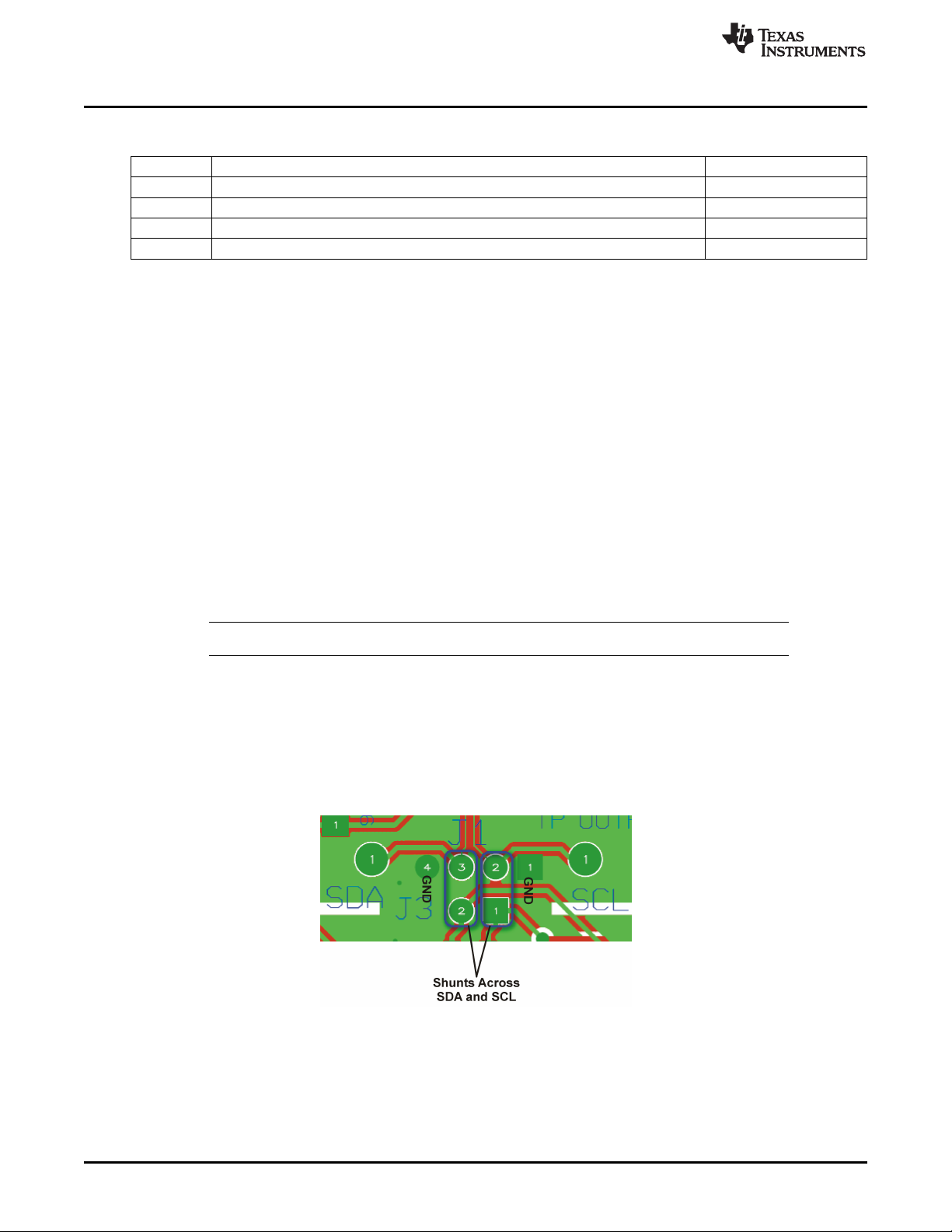
4. Install shunts in J1 and J3 as shown in Figure 1. This sets the TPA2028D1 to accept I2C inputs from
the EVM itself.
Figure 1. Place Shunts Horizontally Across SDA and SCL
2
TPA2028D1YZFEVM SLOU283–February 2010
Copyright © 2010, Texas Instruments Incorporated
Submit Documentation Feedback
Page 3
www.ti.com
5. Powering the EVM:
6. Connect audio source to RCA jacks IN.
7. Connect speakers (8 Ω to 32 Ω) to the output banana jacks OUTP and OUTM.
8. Plug in USB.
9. Turn on the power supply.
10. If this is the first time a TPA2028D1YZFEVM is plugged in after installing the software, follow the
Operation
• The EVM can be powered via USB connection or by external power supply:
(a) Via USB power: Install shunt for USBPWR if USB power is used.
(b) External power supply: connect an external regulated power supply adjusted for 2.5 V–5.5 V to the
VDD and GND banana jacks, taking care to observe marked polarity. Make sure USBPWR is
removed in this case.
Note:
(a) USB interface may not be able to provide enough current. For best audio performance, use
external power supply.
(b) Make sure only one power source is used. Connecting two power sources will cause damage
to the device and the supply.
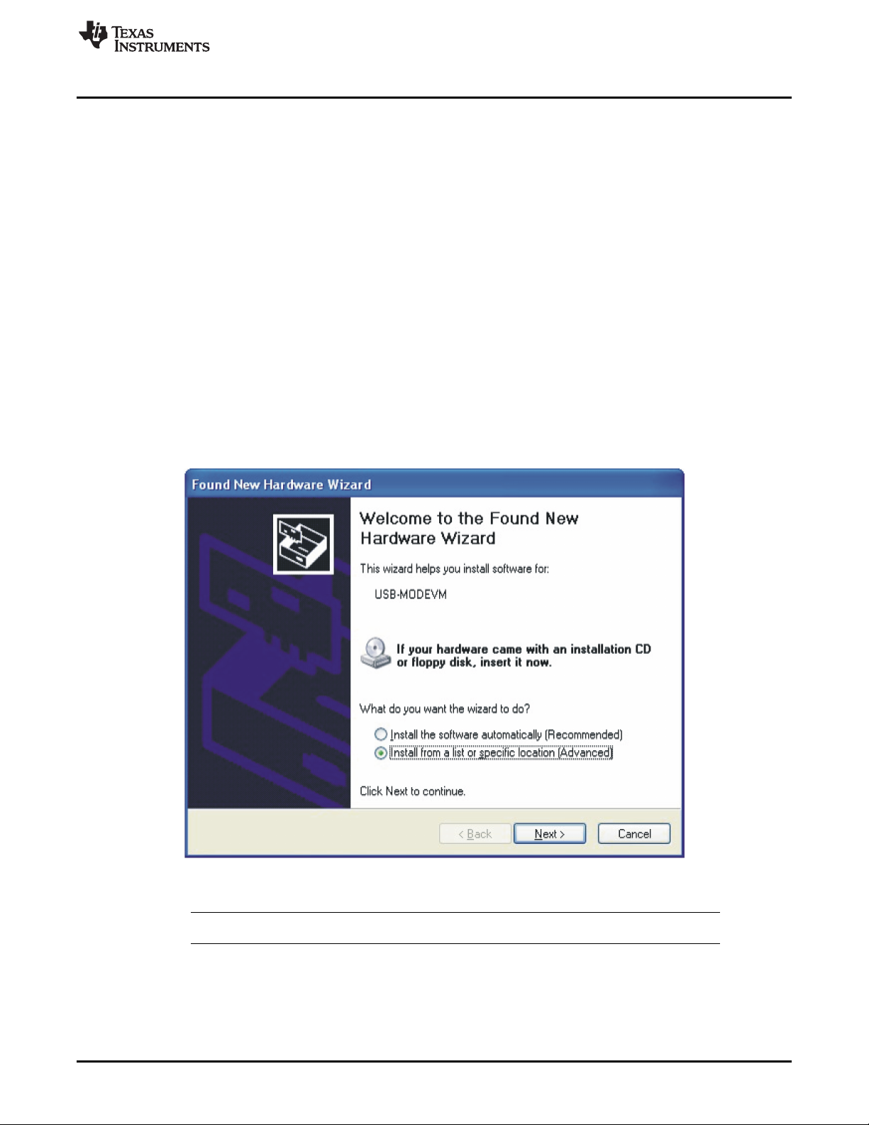
Windows dialog (Figure 2), questions, and selections:
(a) Select "Install from a list or specific location (Advanced)", then click next.
(1)
(b) Browse to the folder where the TPA2028D1 interface is installed then click ok.
(c) Windows will automatically install the driver.
Figure 2. Found New Hardware Wizard Advisory Screen
NOTE: It is not necessary to repeat steps 10. a. to c., once the driver is installed.
(1)
Computer screen images showing Windows XP interface are courtesy of Microsoft Corporation
SLOU283–February 2010 TPA2028D1YZFEVM
Submit Documentation Feedback
Copyright © 2010, Texas Instruments Incorporated
3
Page 4
Operation
2.1.3 Using the Software
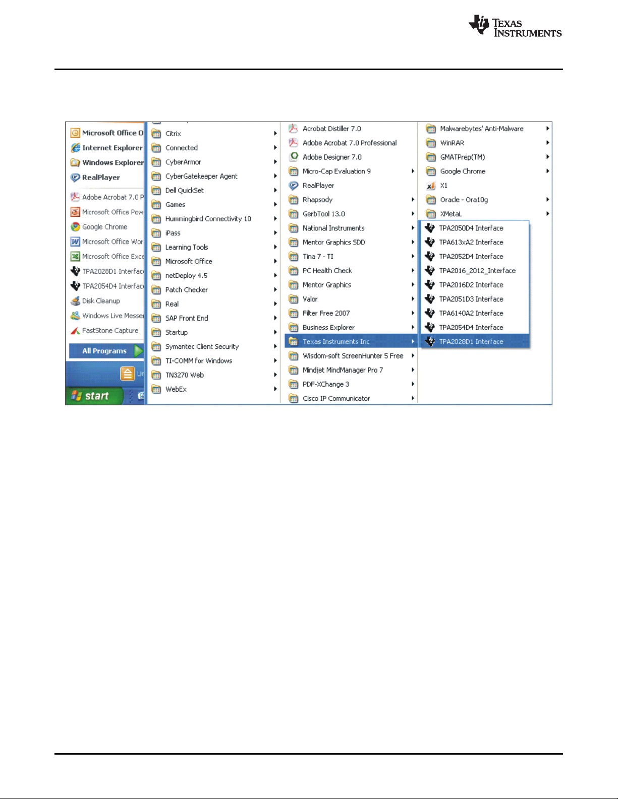
1. Start the TPA2028D1 Interface by clicking the Start menu and clicking on the TPA2028D1 Interface
icon.
www.ti.com
Figure 3. Starting the Software
2. The TPA2028D1 software interface is as shown in Figure 4.
4
TPA2028D1YZFEVM SLOU283–February 2010
Copyright © 2010, Texas Instruments Incorporated
Submit Documentation Feedback
Page 5

www.ti.com
Operation
Figure 4. Software Interface
NOTE: The TPA2028D1 powers up with the amplifier in software shutdown. To hear an output,
uncheck shutdown.
3. Uncheck and check SPK_EN to place the Class-D output in and out of CHANNEL SHUTDOWN.
4. Click Shutdown to place the TPA2028D1 in and out of SOFTWARE SHUTDOWN.
5. Adjust the Attack Time, Release Time and Hold Time by sliding the bar or clicking the tap in the GUI.
You can also type a value in the box; in that case, the value will be rounded to the closest available
setting.
6. Adjust the Fixed Gain, Maximum Gain and Limiter Level by dragging the bar or clicking the tap in the
GUI. You can also type a value in the box; in that case, the value will be rounded to the closest
available setting.
7. Adjust Compression Ratio and Noise Gate Threshold by clicking the value.
8. The Limiter Power Level can be calculated by selecting the Load Resistance.
9. I2C Status box reports the status of I2C communications. An error or failure has occurred if it shows
I2C failure.
10. To read the I2C status, click Refresh.
11. Thermal box reports the status of thermal failure. A thermal fault has occurred if it turns red.
12. Click Show Graph to display the AGC transfer function. The transfer function is automatically updated
with the current AGC parameters (fixed gain, maximum gain, limiter level and compression) in GUI.
Click Hide Graph to hide the transfer function.
13. Volume Macro simulates volume control by changing fixed gain, limiter level and maximum gain
simultaneously. Follow the steps below to use the Volume Marco.
• At the top left corner of the GUI, select Volume Macro.
• Slide the volume bar to adjust the volume.
• Click Volume Marco again to go back to GUI.
• Click refresh to update the AGC parameters.
14. The GUI has a built-in I2C programming interface. Follow the steps below to use the I2C programming
function.
• At the top left corner of the GUI, click File to access the I2C programming interface.
SLOU283–February 2010 TPA2028D1YZFEVM
Submit Documentation Feedback
Copyright © 2010, Texas Instruments Incorporated
5
Page 6

Operation
• Save Script can record the current register values. Select Save Script >> Click the folder icon to
browse to the place where you want to save the script >> name the file in text format, then select
OK to save.
• Load Script can load the previously saved script to program the entire register file. Select Load
Script >> Click the folder icon to browse to the place where the script is located >> Select the file
then click OK >> Click Load.
• I2C interface can program individual register value of TPA2028D1. Select I2C Interface >> I2C
address is xB0, which is the address of TPA2028D1. Device address is from 1 to 7, which is the
register address of TPA2028D1.
2.1.4 Shutdown Control
The TPA2028D1 EVM provides independent hardware shutdown controls for the Class-D power amplifier
and the USB controller.
1. Press and hold push button S1 to shutdown TPA2028D1. Release S1 to activate TPA2028D1.
2. Press and hold push button S2 to shutdown the USB controller. Release S2 to activate the USB
controller.
2.2 Quick Start List When Connected to Existing Circuits With I2C Controls
The TPA2028D1YZFEVM can be easily connected to existing circuits with I2C controls. Connections to the
EVM module can be made using banana plugs for the power supply. The inputs accept standard RCA
plugs and the outputs accept banana connectors.
www.ti.com
2.2.1 Evaluation Module Preparations
1. Ensure that all external power sources are set to OFF.
2. Install shunts in jumpers JP4.
3. Remove shunts between J1 and J3 and connect I2C controls to J1 as shown in Figure 5.
Figure 5. Connect I2C Controls to JP3
4. Install shunts in jumpers JP2 when single-ended audio input is used; this ties IN– to ground.
5. Remove USBPWR.
6. Connect an external regulated power supply adjusted for 2.5 V–5.5 V to the VDD and GND banana
jacks, taking care to observe marked polarity.
7. Connect audio source to IN.
8. Connect speakers (8 Ω to 32 Ω) to the output banana jacks OUTP and OUTM.
9. Turn on power supply.
6
TPA2028D1YZFEVM SLOU283–February 2010
Copyright © 2010, Texas Instruments Incorporated
Submit Documentation Feedback
Page 7

P1.0
USB+
VDD
JP2
S1
C5
0603
1000pfd/50V
C4
0603
1000pfd/50V
C6
0603
4700pfd/50V
C7
0603
4700pfd/50V
GND
GND
GND
GND
GND
GND
GND
GND
GND
GND
GND
R1
0603
100K
C1
0603
1.0ufd/10V
C2
0603
1.0ufd/10V
C3
0603
1.0ufd/10V
R2
DNP
0805
1.0K
R3
DNP
0805
1.0K
RCA(Black)
IN
FROMTAS1020
GND
Vdd
GND
DNP
JP_IN
DNP
JP_VDD
DNP
JP_OUT
GND
OUTP
OUTM
TP OUTP
White
TP OUTM
White
TP GND
Black
SDA
White
SCL
White
FB1
0805
FB2
0805
C21
0603
DNP
USB PWR
C8
1206
10ufd/6.3V
VDD
GND
+3.3VD
USB+
R16
0805
0.0
WCSP9-YZF
A3
A2
B3
C3
C1
B1
C2 A1
B2
TPA2028D1YZF
U1
FROMCONTROLLERJ3
J1
Q1
BSS138ZXCT
SOT23-DBV3
D
G
S
MEASUREMENT FILTER
www.ti.com
3 TPA2028D1YZFEVM Schematic
TPA2028D1YZFEVM Schematic
Figure 6. TPA2028D1YZFEVM – YZF-Device Schematic, Page 1
SLOU283–February 2010 TPA2028D1YZFEVM
Submit Documentation Feedback
Copyright © 2010, Texas Instruments Incorporated
7
Page 8

USB+
P1.0
MRESET~
JP4
+3.3VD
+3.3VD
+3.3VD
+3.3VD
+3.3VD
+3.3VD
+3.3VD
GND
GND
GND
GND
GND
GND
GND
GND
GND
GND
GND
GND
GND
GND
GND
GND
GND
GND
27.4
0603
R8
27.4
0603
R9
S2
3.3V/500mA
SOP8-D
VR1
100K
0603
R13
100K
0603
R11
3.09K
0603
R10
1.50K
0603
R7
TAS1020BPFB
24LC64-I/SN
SOP8-D(SOIC)
U2
600 OHMS
0805
FB3
600 OHMS
0805
FB4
USB MINIB
J2
NC
NC
Case
Case
Case
Case
Data+
GND
ID_NC
5v
Data-
100ufd/10V
C18
TANT2412
+
6.00MHz
HC49/US
Y1
2.00K
0603
R12
2.00K
0603
R5
2.00K
0603
R6
0.0
0805
R15
0.1ufd/10V
0603
C17
0.1ufd/10V
0603
C19
0.1ufd/10V
0603
C15
33pfd/50V
0603
C11
33pfd/50V
0603
C12
1000pfd/50V
0603
C14
0.1ufd/10V
0603
C20
47pfd/50v
0603
C9
47pfd/50v
0603
C10
10ufd/6.3V
1206
C16
USB+
100pfd/50V
0603
C13
J3
TO
TPA2028D1
EN
SCL
SDA
J1
4
3
2
1
TPA2028D1YZFEVM Schematic
www.ti.com
Figure 7. TPA2028D1YZFEVM – YZF-Device Schematic, Page 2
8
TPA2028D1YZFEVM SLOU283–February 2010
Copyright © 2010, Texas Instruments Incorporated
Submit Documentation Feedback
Page 9

DB
DB
www.ti.com
4 TPA2028D1YZFEVM PCB Layers
TPA2028D1YZFEVM PCB Layers
Figure 8. TPA2028DYZF1EVM – YZF-Device Top Layer
Figure 9. TPA2028D1YZFEVM – YZF-Device Bottom Layer
SLOU283–February 2010 TPA2028D1YZFEVM
Submit Documentation Feedback
Copyright © 2010, Texas Instruments Incorporated
9
Page 10

TPA2028D1YZFEVM Parts List
www.ti.com
5 TPA2028D1YZFEVM Parts List
Table 1. Bill of Materials for TPA2028D1YZFEVM
Ref Des Description QTY MFR Part No. MFR Vendor Part No. Vendor
TI SEMICONDUCTORS
U5 1.7 W Mono speaker driver W/AGC I2C CTRL, 1 TPA2028D1YZF Texas TPA2028D1YZF Texas
VR1 VOLT REG 3.3V 500mA LDO fast transient response 1 TPS77533D Texas 296-2776-5 Digi-Key
U4 USB Streaming controller TQFP48-PFB ROHS 1 TAS1020BPFB Texas 296-13041-5 Digi-Key
U2 64K I2C SERIAL EEPROM SOP8-D 1 24LC64-I/SN Microchip 24LC64-I/SN Digi-Key
Q1 N-CH Enhancement mode VERT DMOS FET 1 BSS138TA Zetex BSS138ZXCT Digi-Key
Y1 Crystal, 6.000 MHz, SMT-HC49/US CSM-7 ROHS 1 ECS-60-32-5PXDN-TR ECS XC1295CT Digi-Key
C11,C12 CAP 33 pF 50V 5% CERM 0603 NPO ROHS 2 ECJ-1VC1H330J Panasonic PCC330ACVCT Digi-Key
C9, C10 CAP 47 pF 50V 5% CERM 0603 NPO ROHS 2 ECJ-1VC1H470J Panasonic PCC470ACVCT Digi-Key
C13 CAP 100 pF 50V 5% CERM 0603 NPO ROHS 1 ECJ-1VC1H101J Panasonic PCC101ACVCT Digi-Key
C14 CAP 1000 pF 50V 5% CERM 0603 COG ROHS 1 C1608C0G1H102J TDK Corp. 445-1293-1 Digi-Key
C6, C7 CAP 4700 pF 50V CERM 0603 X7R ROHS 2 ECJ-1VB1H472K Panasonic PCC1780CT Digi-Key
C15, C17, CAP SMT0603 CERM 0.1mF 10V 5% X7R ROHS 4 C0603C104K8RACTU Kemet 399-1095-1 Digi-Key
C19, C20
C1–C3 CAP 1.0 mF 10V 10% CERM 0603 X5R ROHS 3 ECJ-1VB1A105K Panasonic PCC2174CT Digi-Key
C8, C16 CAP 10 mF 6.3V 10% CERM 1206 X5R ROHS 2 C3216X5R0J106K TDK 445-1388-1 Digi-Key
C18 CAP TANT2412 100 mF 10V 10% B45197A ROHS 1 B45197A2107K309 Kemet 495-1528-1 Digi-Key
R15, R16 RES 0Ω 1/8W 5% SMD 0805 ROHS 2 ERJ-6GEY0R00V Panasonic P0.0ACT Digi-Key
R8, R9 RESISTOR SMD0603 27.4 Ω 1/10W 1% ROHS 2 CRCW060327R4FKEA Vishay 541-27.4HCT Digi-Key
R7 RES SMD0603 1.50 kΩ 1/10W 1% ROHS 1 ERJ-3EKF1501V Panasonic P1.50KHCT Digi-Key
R5, R6, R12 RES 2.00 kΩ 1/16W 1% SMD 0603 ROHS 3 ERJ-3EKF2001V Panasonic P2.00KHCT Digi-Key
R10 RES 3.09kΩ 1/10W 1% SMD 0603 ROHS 1 ERJ-3EKF3091V Panasonic P3.09KHCT Digi-Key
R1, R11, R13 RES 100 kΩ 1/16W 1% SMD 0603 ROHS 3 ERJ-3EKF1003V Panasonic P100KHCT Digi-Key
FB3, FB4 Ferrite SMD0805 600 Ω 0.24 A RDC=0.14 ROHS 2 MMZ2012R601A TDK 445-1554-1 Digi-Key
FB1, FB2 Ferrite bead SMD0805 80 Ω at 100 MHz 5A ROHS 2 HI0805R800R-10 Steward 240-2395-1 Digi-Key
J3, JP2, JP4, Header 2 Pin, PCB 2,0 mm ROHS 4 26630201RP2 Norcomp 2663S-02 Digi-Key
USB PWR
J1 Header 4 Pin, PCB 2,0 mm ROHS 1 26630401RP2 Norcomp 2663S-04 Digi-Key
IN Jack, RCA 3-Pin PCB-RA Black ROHS 1 PJRAN1X1U01X Switchcraft 65K7770 NEWARK
J2 Jack USB MINIB SMT-RA 5Pin ROHS 1 UX60-MB-5ST Hirose H2959CT Digi-Key
WCSP9-YZF ROHS Instruments Instruments
SOP8-D ROHS Instruments
Instruments
SEMICONDUCTIORS
SOT23-DBV3 ROHS
CAPACITORS
RESISTORS
FERRITE BEADS
HEADERS AND JACKS
10
TPA2028D1YZFEVM SLOU283–February 2010
Submit Documentation Feedback
Copyright © 2010, Texas Instruments Incorporated
Page 11

www.ti.com
TPA2028D1YZFEVM Parts List
Table 1. Bill of Materials for TPA2028D1YZFEVM (continued)
Ref Des Description QTY MFR Part No. MFR Vendor Part No. Vendor
TESTPOINTS AND SWITCHES
SCL, SDA, PC Testpoint, white, ROHS 4 5002 Keystone 5002K Digi-Key
TP OUTM, Electronics
TP OUTP
TP GND PC Testpoint, black, ROHS 1 5001 Keystone 5001K Digi-Key
S1, S2 Switch, MOM, 160G SMT 4X3MM ROHS 2 TL1015AF160QG E-Switch EG4344CT Digi-Key
SHUNTS
JP2, JP4 Shunt, black AU Flash 2mmLS 2 810-002-SP2L001 Norcomp SP2-001E Digi-Key
BINDING POSTS
GND, Binding-post, NONINS, THRU, ROHS 4 111-2223-001 Emerson J587 Digi-Key
VDD,OUTM, NPCS
OUTP
STANDOFFS AND HARDWARE
HW1–HW4 Standoff ,4-40 0.5 in 3/16 in Diameter ALUM RND F-F 4 2027 Keystone 2027K Digi-Key
HW1–HW4 4-40 Screw, Steel 0.250 IN 4 PMS 440 0025 PH Building H342 Digi-Key
COMPONENTS NOT ASSEMBLED
C21, C4, C5, R2, R3, JP_VDD, JP_VOUT, JP_VIN
Electronics
INC.
Fasteners
SLOU283–February 2010 TPA2028D1YZFEVM
Submit Documentation Feedback
Copyright © 2010, Texas Instruments Incorporated
11
Page 12

EVALUATION BOARD/KIT IMPORTANT NOTICE
Texas Instruments (TI) provides the enclosed product(s) under the following conditions:
This evaluation board/kit is intended for use for ENGINEERING DEVELOPMENT, DEMONSTRATION, OR EVALUATION PURPOSES
ONLY and is not considered by TI to be a finished end-product fit for general consumer use. Persons handling the product(s) must have
electronics training and observe good engineering practice standards. As such, the goods being provided are not intended to be complete
in terms of required design-, marketing-, and/or manufacturing-related protective considerations, including product safety and environmental
measures typically found in end products that incorporate such semiconductor components or circuit boards. This evaluation board/kit does
not fall within the scope of the European Union directives regarding electromagnetic compatibility, restricted substances (RoHS), recycling
(WEEE), FCC, CE or UL, and therefore may not meet the technical requirements of these directives or other related directives.
Should this evaluation board/kit not meet the specifications indicated in the User’s Guide, the board/kit may be returned within 30 days from
the date of delivery for a full refund. THE FOREGOING WARRANTY IS THE EXCLUSIVE WARRANTY MADE BY SELLER TO BUYER
AND IS IN LIEU OF ALL OTHER WARRANTIES, EXPRESSED, IMPLIED, OR STATUTORY, INCLUDING ANY WARRANTY OF
MERCHANTABILITY OR FITNESS FOR ANY PARTICULAR PURPOSE.
The user assumes all responsibility and liability for proper and safe handling of the goods. Further, the user indemnifies TI from all claims
arising from the handling or use of the goods. Due to the open construction of the product, it is the user’s responsibility to take any and all
appropriate precautions with regard to electrostatic discharge.
EXCEPT TO THE EXTENT OF THE INDEMNITY SET FORTH ABOVE, NEITHER PARTY SHALL BE LIABLE TO THE OTHER FOR ANY
INDIRECT, SPECIAL, INCIDENTAL, OR CONSEQUENTIAL DAMAGES.
TI currently deals with a variety of customers for products, and therefore our arrangement with the user is not exclusive.
TI assumes no liability for applications assistance, customer product design, software performance, or infringement of patents or
services described herein.
Please read the User’s Guide and, specifically, the Warnings and Restrictions notice in the User’s Guide prior to handling the product. This
notice contains important safety information about temperatures and voltages. For additional information on TI’s environmental and/or
safety programs, please contact the TI application engineer or visit www.ti.com/esh.
No license is granted under any patent right or other intellectual property right of TI covering or relating to any machine, process, or
combination in which such TI products or services might be or are used.
FCC Warning
This evaluation board/kit is intended for use for ENGINEERING DEVELOPMENT, DEMONSTRATION, OR EVALUATION PURPOSES
ONLY and is not considered by TI to be a finished end-product fit for general consumer use. It generates, uses, and can radiate radio
frequency energy and has not been tested for compliance with the limits of computing devices pursuant to part 15 of FCC rules, which are
designed to provide reasonable protection against radio frequency interference. Operation of this equipment in other environments may
cause interference with radio communications, in which case the user at his own expense will be required to take whatever measures may
be required to correct this interference.
EVM WARNINGS AND RESTRICTIONS
It is important to operate this EVM within the supply voltage range of –0.3 V to 6 V and the input voltage range of –0.3 V to VDD +0.3 .
Exceeding the specified input range may cause unexpected operation and/or irreversible damage to the EVM. If there are questions
concerning the input range, please contact a TI field representative prior to connecting the input power.
Applying loads outside of the specified output range may result in unintended operation and/or possible permanent damage to the EVM.
Please consult the EVM User's Guide prior to connecting any load to the EVM output. If there is uncertainty as to the load specification,
please contact a TI field representative.
During normal operation, some circuit components may have case temperatures greater than 85°C. The EVM is designed to operate
properly with certain components above 85°C as long as the input and output ranges are maintained. These components include but are
not limited to linear regulators, switching transistors, pass transistors, and current sense resistors. These types of devices can be identified
using the EVM schematic located in the EVM User's Guide. When placing measurement probes near these devices during operation,
please be aware that these devices may be very warm to the touch.
Mailing Address: Texas Instruments, Post Office Box 655303, Dallas, Texas 75265
Copyright © 2009, Texas Instruments Incorporated
 Loading...