

Page 1
YZH
AVDD
INL–
INL+
AGND
PGND
OUTL+
OUTL–
PVDDR
10 Fm
ToBattery
SDA
INR–
INR+
C 1 FINm
OUTR+
OUTR–
SCL
SDZ
I CClock
2
I CData
2
MasterShutdown
TPA2026D2
Digital
Baseband
Analog
Baseband
or
Codec
PVDDL
TPA2026D2
www.ti.com
SLOS649 –MARCH 2010
3.2-W/Ch Stereo Class-D Audio Amplifier with Fast Gain Ramp SmartGain™ AGC/DRC
Check for Samples: TPA2026D2
1
FEATURES
23
• Fast AGC Start-up Time: 5 ms
• Pin-Out Compatible with TPA2016D2
• Filter-Free Class-D Architecture
• 3.2 W/Ch Into 4 Ω at 5 V (10% THD+N)
• 750 mW/Ch Into 8 Ω at 3.6 V (10% THD+N)
• Power Supply Range: 2.5 V to 5.5 V
• Flexible Operation With/Without I2C
• Programmable DRC/AGC Parameters
• Digital I2C Volume Control
• Selectable Gain from 0 dB to 30 dB in 1-dB speaker from damage at high power levels and
Steps
• Selectable Attack, Release and Hold Times
• 4 Selectable Compression Ratios
• Low Supply Current: 3.5 mA
• Low Shutdown Current: 0.2 mA
• High PSRR: 80 dB
• AGC Enable/Disable Function
• Limiter Enable/Disable Function
• Short-Circuit and Thermal Protection
• Space-Saving Package
– 2,2 mm × 2,2 mm Nano-Free™ WCSP (YZH)
DESCRIPTION
The TPA2026D2 is a stereo, filter-free Class-D audio
power amplifier with volume control, dynamic range
compression (DRC) and automatic gain control
(AGC). It is available in a 2.2 mm x 2.2 mm WCSP
package.
The DRC/AGC function in the TPA2026D2 is
programmable via a digital I2C interface. The
DRC/AGC function can be configured to automatically
prevent distortion of the audio signal and enhance
quiet passages that are normally not heard. The
DRC/AGC can also be configured to protect the
compress the dynamic range of music to fit within the
dynamic range of the speaker. The gain can be
selected from 0 dB to +30 dB in 1-dB steps. The
TPA2026D2 is capable of driving 3.2 W/Ch at 5 V
into an 4-Ω load or 750 mW/Ch at 3.6 V into an 8-Ω
load. The device features independent software
shutdown controls for each channel and also provides
thermal and short circuit protection. The TPA2026D2
has faster AGC gain ramp during start-up than
TPA2026D2.
In addition to these features, a fast start-up time and
small package size make the TPA2026D2 an ideal
choice for cellular handsets, PDAs, and other
portable applications.
APPLICATIONS
• Wireless or Cellular Handsets and PDAs
• Portable Navigation Devices
• Portable DVD Player
• Notebook PCs
• Portable Radio
• Portable Games
• Educational Toys
• USB Speakers
1
Please be aware that an important notice concerning availability, standard warranty, and use in critical applications of Texas
Instruments semiconductor products and disclaimers thereto appears at the end of this data sheet.
2SmartGain, Nano-Free are trademarks of Texas Instruments.
3All other trademarks are the property of their respective owners.
PRODUCTION DATA information is current as of publication date.
Products conform to specifications per the terms of the Texas
Instruments standard warranty. Production processing does not
necessarily include testing of all parameters.
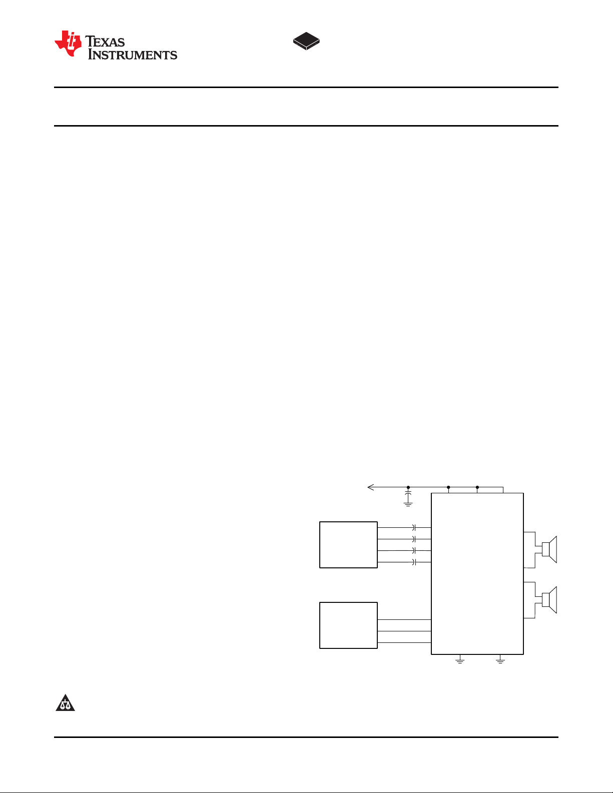
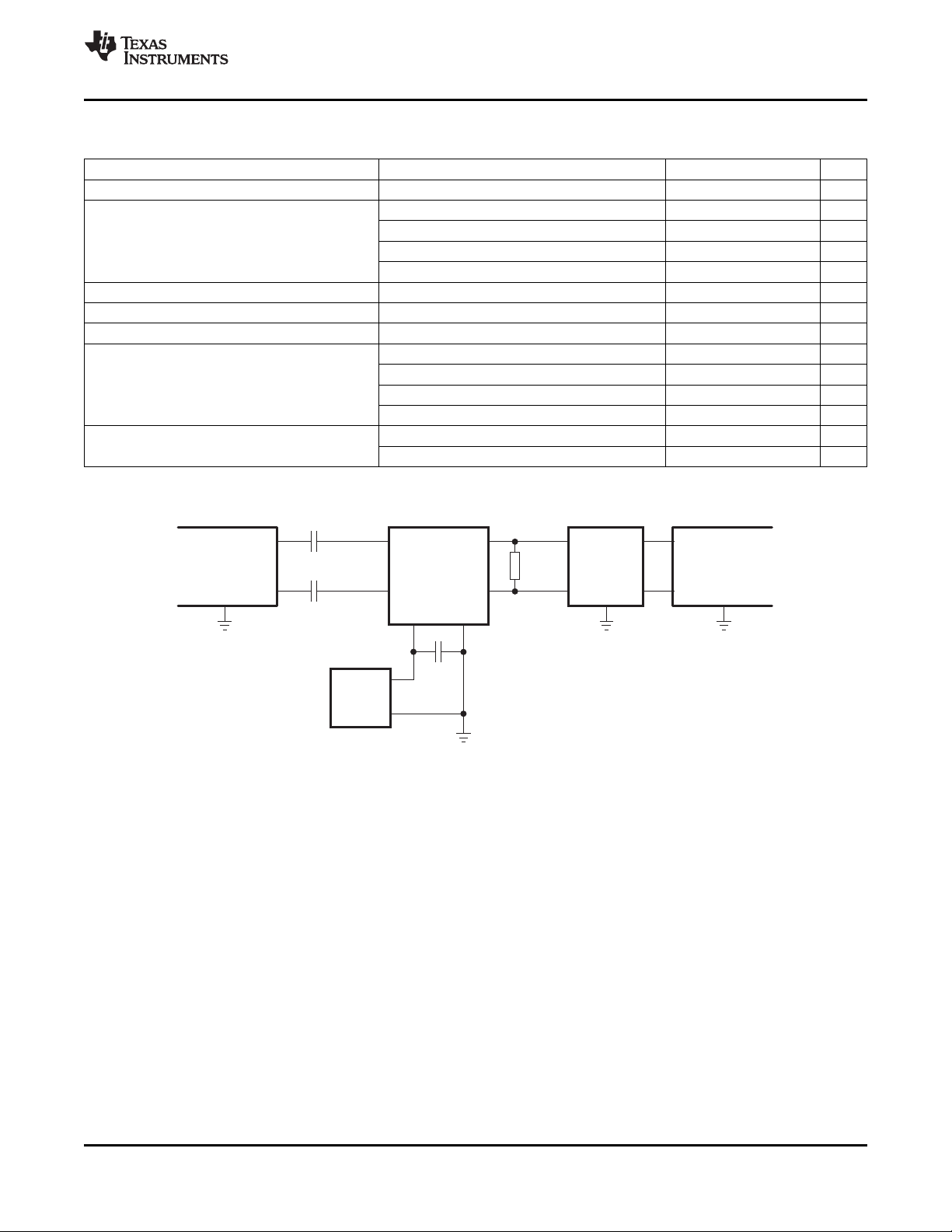
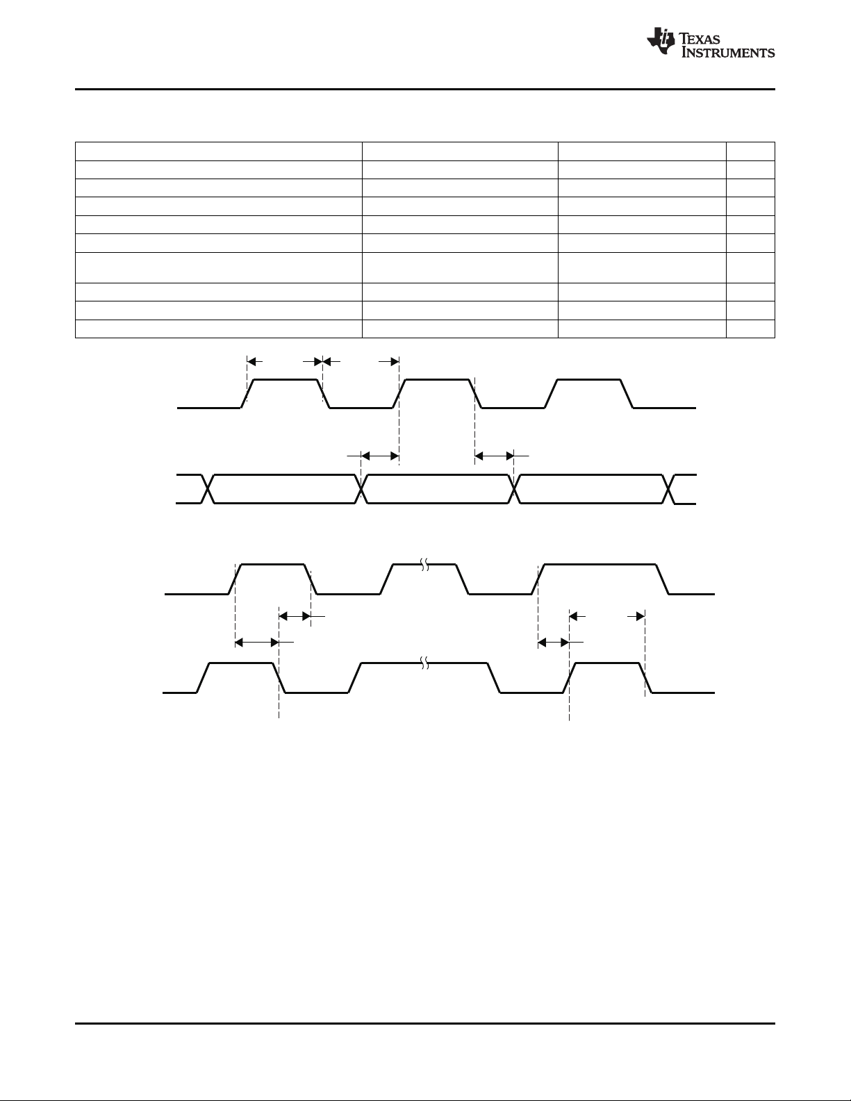
SIMPLIFIED APPLICATION DIAGRAM
Copyright © 2010, Texas Instruments Incorporated
Page 2
I2C Interface
& Control
INL+
INL-
SDA
OUTL+
OUTL-
SDZ
INR+
INR-
SCL
Class-D
Modulator
Volume
Control
Differential
Input Left
C
IN
1uF
Differential
Input Right
C
IN
1uF
I2C Interface
IC shutdown
Power
Stage
AGC
Reference
Volume
Control
Power
Stage
OUTR+
OUTR-
AGND PGND
Bias and
References
AVDD
PVDDR
PVDDL
AGC
Class-D
Modulator
PGND
OUTL–OUTR–OUTR+
INL–INR+ INL+INR–
AGNDSDASCLAVDD
PVDDLSDZPVDDR
OUTL+
D 1 D 2 D 3 D 4
C 1 C 2 C 3 C 4
B1 B3 B4B2
A1 A2 A3 A4
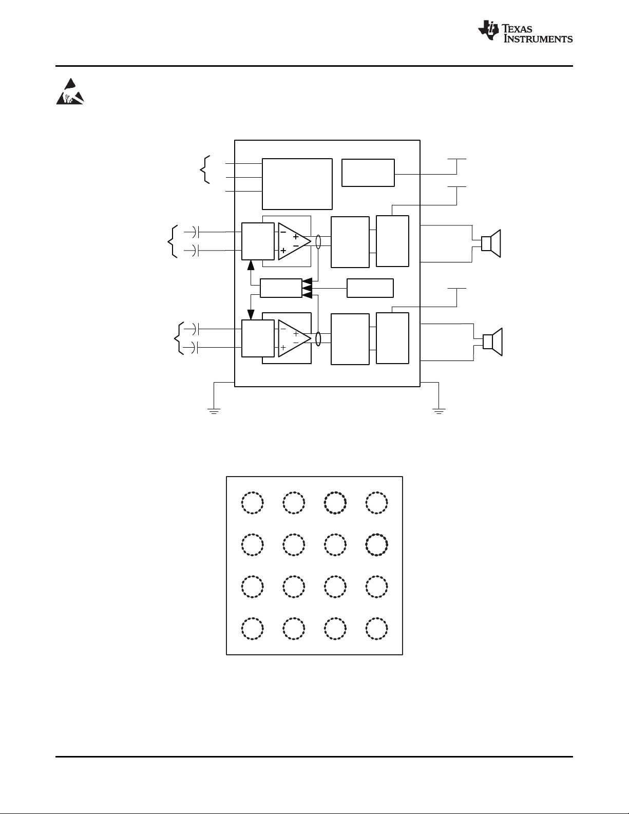
YZH(WCSP)PACKAGE
(TopView)
TPA2026D2
SLOS649 –MARCH 2010
These devices have limited built-in ESD protection. The leads should be shorted together or the device placed in conductive foam
during storage or handling to prevent electrostatic damage to the MOS gates.
www.ti.com
FUNCTIONAL BLOCK DIAGRAM
DEVICE PINOUT
2 Submit Documentation Feedback Copyright © 2010, Texas Instruments Incorporated
Product Folder Link(s): TPA2026D2
Page 3
TPA2026D2
www.ti.com
PIN FUNCTIONS
PIN
NAME WCSP
INR+ A2 I Right channel positive audio input
INR– A1 I Right channel negative audio input
INL+ A3 I Left channel positive audio input
INL– A4 I Left channel negative audio input
SDZ C2 I Shutdown terminal (active low)
SDA B3 I/O I2C data interface
SCL B2 I I2C clock interface
OUTR+ D1 O Right channel positive differential output
OUTR– D2 O Right channel negative differential output
OUTL+ D4 O Left channel positive differential output
OUTL– D3 O Left channel negative differential output
AVDD B1 P Analog supply (must be the same as PVDDR and PVDDL)
AGND B4 P Analog ground (all GND pins need to be connected)
PVDDR C1 P Right channel power supply (must be the same as AVDD and PVDDL)
PGND C3 P Power ground (all GND pins need to be connected)
PVDDL C4 P Left channel power supply (must be the same as AVDD and PVDDR)
I/O/P DESCRIPTION
SLOS649 –MARCH 2010
ABSOLUTE MAXIMUM RATINGS
(1)
over operating free-air temperature range (unless otherwise noted).
VALUE / UNIT
V
Supply voltage AVDD, PVDDR, PVDDL –0.3 V to 6 V
DD
Input voltage
Continuous total power dissipation
T
Operating free-air temperature range –40°C to 85°C
A
T
Operating junction temperature range –40°C to 150°C
J
T
Storage temperature range –65°C to 150°C
stg
ESD Electro-static discharge tolerance, all pins
R
Minimum load resistance 3.2 Ω
L
(1) Stresses beyond those listed under "absolute maximum ratings" may cause permanent damage to the device. These are stress ratings
only, and functional operation of the device at these or any other conditions beyond those indicated under "recommended operating
conditions" is not implied. Exposure to absolute-maximum-rated conditions for extended periods may affect device reliability.
DISSIPATION RATINGS TABLE
PACKAGE TA≤ 25°C DERATING FACTOR TA= 70°C TA= 85°C
16-ball WCSP 1.25 W 10 mW/°C 0.8 W 0.65 W
(1) Dissipations ratings are for a 2-side, 2-plane PCB.
SDZ, INR+, INR–, INL+, INL– –0.3 V to VDD+0.3 V
SDA, SCL –0.3 V to 6 V
See Dissipation Ratings
Table
Human body model (HBM) 2 KV
Charged device model (CDM) 500 V
(1)
Copyright © 2010, Texas Instruments Incorporated Submit Documentation Feedback 3
Product Folder Link(s): TPA2026D2
Page 4
TPA2026D2
SLOS649 –MARCH 2010
T
A
–40°C to 85°C
AVAILABLE OPTIONS
PACKAGED DEVICE
16-ball, 2,2 mm × 2,2 mm WCSP (+0.01 mm/
-0.09 mm tolerance)
(2)
(1)
PART NUMBER SYMBOL
TPA2026D2 YZHR NSV
TPA2026D2 YZHT NSV
www.ti.com
(1) For the most current package and ordering information, see the Package Option Addendum at the end of this document, or see the TI
Web site at www.ti.com
(2) The YZH package is only available taped and reeled. The suffix R indicates a reel of 3000; the suffix T indicates a reel of 250.
RECOMMENDED OPERATING CONDITIONS
MIN MAX UNIT
VDDSupply voltage AVDD, PVDDR, PVDDL 2.5 5.5 V
VIHHigh-level input voltage SDZ, SDA, SCL 1.3 V
VILLow-level input voltage SDZ, SDA, SCL 0.6 V
T
Operating free-air temperature –40 +85 °C
A
ELECTRICAL CHARACTERISTICS
at TA= 25°C, VDD= 3.6 V, SDZ = 1.3 V, and RL= 8 Ω + 33 mH (unless otherwise noted).
PARAMETER TEST CONDITIONS MIN TYP MAX UNIT
V
DD
I
SDZ
I
SWS
I
DD
f
SW
I
IH
I
IL
t
START
POR Power on reset ON threshold 2 2.3 V
POR Power on reset hysteresis 0.2 V
CMRR Input common mode rejection –70 dB
V
oo
Z
OUT
PSRR Power supply rejection ratio VDD= 2.5 V to 4.7 V -80 dB
Supply voltage range 2.5 3.6 5.5 V
SDZ = 0.35 V, VDD= 2.5 V 0.1 1
Shutdown quiescent current SDZ = 0.35 V, VDD= 3.6 V 0.2 1 µA
SDZ = 0.35 V, VDD= 5.5 V 0.3 1
SDZ = 1.3 V, VDD= 2.5 V 35 50
Software shutdown quiescent
current
SDZ = 1.3 V, VDD= 3.6 V 50 70 µA
SDZ = 1.3 V, VDD= 5.5 V 75 110
VDD= 2.5 V 3.5 4.5
Supply current VDD= 3.6 V 3.7 4.7 mA
VDD= 5.5 V 4.5 5.5
Class D switching frequency 275 300 325 kHz
High-level input current VDD= 5.5 V, SDZ = 5.8 V 1 µA
Low-level input current VDD= 5.5 V, SDZ = –0.3 V –1 µA
Start-up time 2.5 V ≤ VDD≤ 5.5 V no pop, CIN≤ 1 mF 5 ms
RL= 8 Ω, V
differential inputs shorted
Output offset voltage 2 10 mV
Output impedance in shutdown 2 kΩ
mode
VDD= 3.6 V, AV= 6 dB, RL= 8 Ω, inputs ac
grounded
SDZ = 0.35 V
= 0.5 V and V
icm
= VDD– 0.8 V,
icm
Gain accuracy Compression and limiter disabled, Gain = 0 to 30 dB –0.5 0.5 dB
4 Submit Documentation Feedback Copyright © 2010, Texas Instruments Incorporated
Product Folder Link(s): TPA2026D2
Page 5
TPA2026D2
IN+
IN–
OUT+
OUT–
V
DD
V
DD
GND
C
I
C
I
Measurement
Output
+
+
–
–
Load
30kHz
Low-Pass
Filter
Measurement
Input
+
–
1 Fm
TPA2026D2
www.ti.com
SLOS649 –MARCH 2010
OPERATING CHARACTERISTICS
at TA= 25°C, VDD= 3.6V, SDZ = 1.3 V, RL= 8 Ω +33 mH, and AV= 6 dB (unless otherwise noted).
PARAMETER TEST CONDITIONS MIN TYP MAX UNIT
k
SVR
THD+N Total harmonic distortion + noise
Nfo
Nfo
FR Frequency response Av = 6 dB 20 20000 Hz
Po
h Efficiency
Power-supply ripple rejection ratio VDD= 3.6 Vdc with ac of 200 mVPPat 217 Hz –68 dB
f
= 1 kHz, PO= 550 mW, VDD= 3.6 V 0.1%
aud_in
f
= 1 kHz, PO= 1 W, VDD= 5 V 0.1%
aud_in
f
= 1 kHz, PO= 630 mW, VDD= 3.6 V 1%
aud_in
f
= 1 kHz, PO= 1.4 W, VDD= 5 V 1%
aud_in
Output integrated noise Av = 6 dB 44 mV
nF
Output integrated noise Av = 6 dB floor, A-weighted 33 mV
A
THD+N = 10%, VDD= 5 V, RL= 8 Ω 1.72 W
Maximum output power
max
THD+N = 10%, VDD= 3.6 V, RL= 8 Ω 750 mW
THD+N = 1%, VDD= 5 V, RL= 8 Ω 1.4 W
THD+N = 1% , VDD= 3.6 V, RL= 8 Ω 630 mW
THD+N = 1%, VDD= 3.6 V, RL= 8 Ω, PO= 0.63 W 90%
THD+N = 1%, VDD= 5 V, RL= 8 Ω, PO= 1.4 W 90%
TEST SET-UP FOR GRAPHS
(1) All measurements were taken with a 1-mF CI(unless otherwise noted).
(2) A 33-mH inductor was placed in series with the load resistor to emulate a small speaker for efficiency measurements.
(3) The 30-kHz low-pass filter is required, even if the analyzer has an internal low-pass filter. An RC low-pass filter (1 kΩ
4.7 nF) is used on each output for the data sheet graphs.
Product Folder Link(s): TPA2026D2
Copyright © 2010, Texas Instruments Incorporated Submit Documentation Feedback 5
Page 6
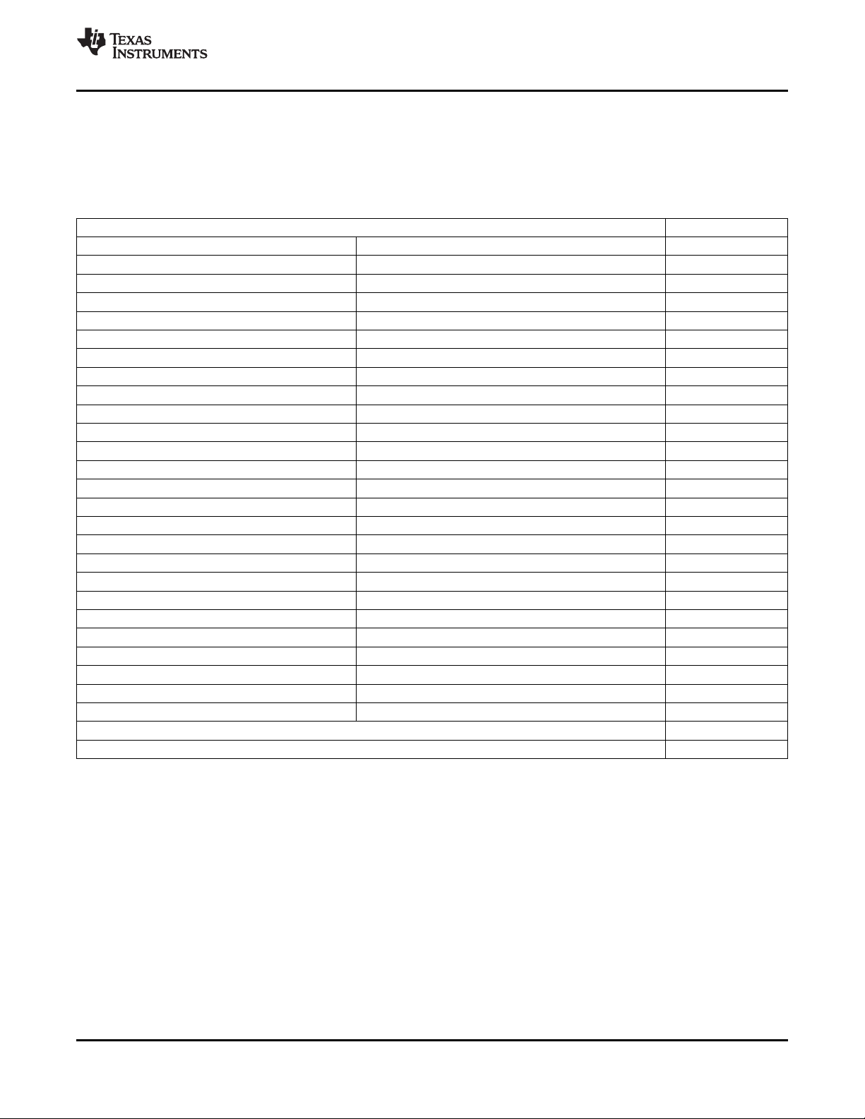
SCL
SDA
t
w(H)
t
w(L)
t
su1
t
h1
SCL
SDA
t
h2
t
(buf)
t
su2
t
su3
StartCondition
StopCondition
TPA2026D2
SLOS649 –MARCH 2010
I2C TIMING CHARACTERISTICS
For I2C Interface Signals Over Recommended Operating Conditions (unless otherwise noted)
PARAMETER TEST CONDITIONS MIN TYP MAX UNIT
f
SCL
t
W(H)
t
W(L)
t
SU(1)
t
h1
t
(buf)
t
SU2
t
h2
t
SU3
Frequency, SCL No wait states 400 kHz
Pulse duration, SCL high 0.6 ms
Pulse duration, SCL low 1.3 ms
Setup time, SDA to SCL 100 ns
Hold time, SCL to SDA 10 ns
Bus free time between stop and start 1.3 ms
condition
Setup time, SCL to start condition 0.6 ms
Hold time, start condition to SCL 0.6 ms
Setup time, SCL to stop condition 0.6 ms
www.ti.com
Figure 1. SCL and SDA Timing
Figure 2. Start and Stop Conditions Timing
6 Submit Documentation Feedback Copyright © 2010, Texas Instruments Incorporated
Product Folder Link(s): TPA2026D2
Page 7
TPA2026D2
www.ti.com
SLOS649 –MARCH 2010
TYPICAL CHARACTERISTICS
with C
(DECOUPLE)
All THD + N graphs are taken with outputs out of phase (unless otherwise noted).
All data is taken on left channel.
= 1 mF, CI= 1 µF.
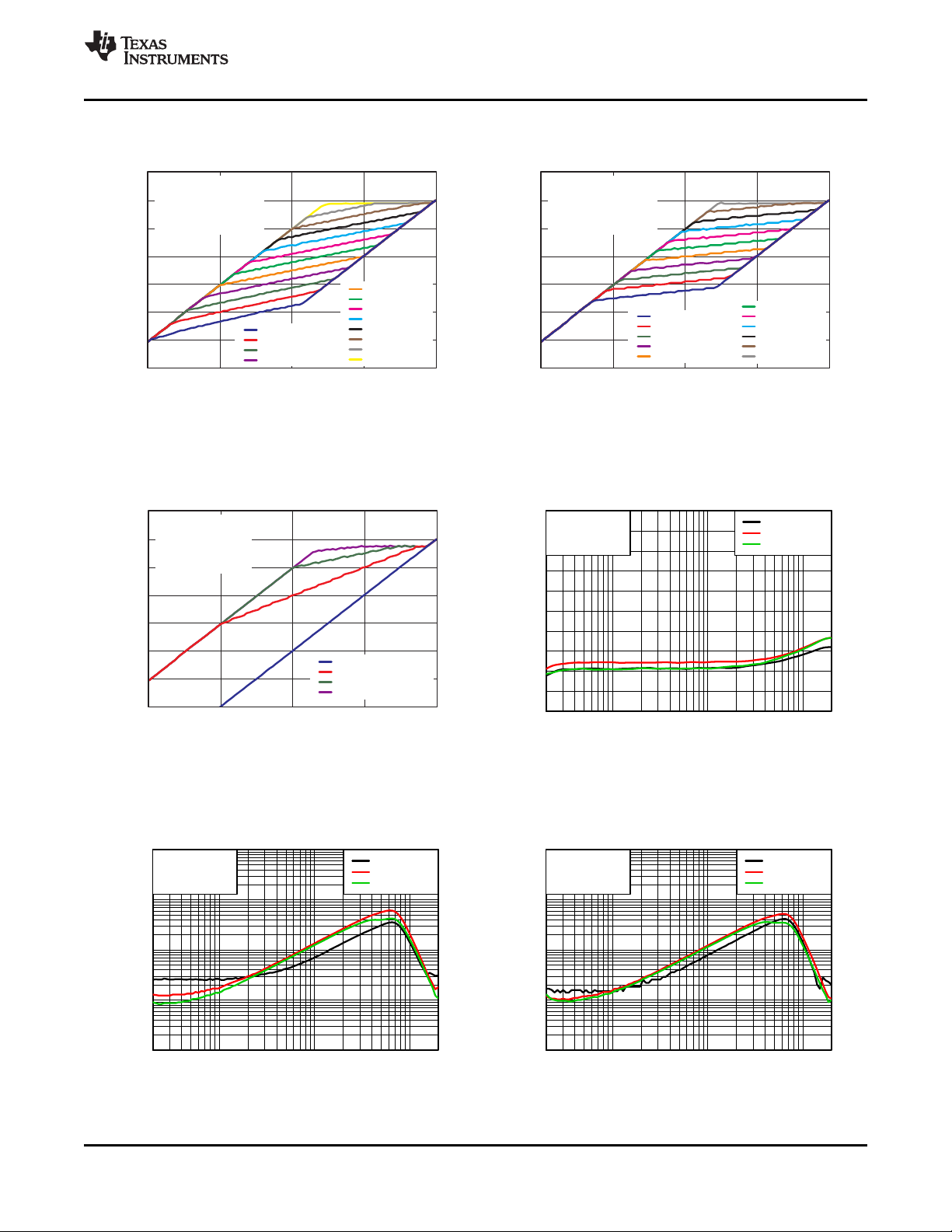
Table of Graphs
FIGURE
Quiescent supply current vs Supply voltage Figure 3
Supply current vs Supply voltage in shutdown Figure 4
Output level vs Input level Figure 5
Output level vs Input level Figure 6
Output level vs Input level Figure 7
Output level vs Input level Figure 8
Output level vs Input level Figure 9
Supply ripple rejection ratio vs Frequency, 8Ω Figure 10
Total harmonic distortion + noise vs Frequency Vsupply = 2.5V, 4Ω Figure 11
Total harmonic distortion + noise vs Frequency Vsupply = 2.5V, 8Ω Figure 12
Total harmonic distortion + noise vs Frequency Vsupply = 3.6V, 4Ω Figure 13
Total harmonic distortion + noise vs Frequency Vsupply = 3.6V, 8Ω Figure 14
Total harmonic distortion + noise vs Frequency Vsupply = 5.0V, 4Ω Figure 15
Total harmonic distortion + noise vs Frequency Vsupply = 5.0V, 8Ω Figure 16
Total harmonic distortion + noise vs Output power, 4Ω Figure 17
Total harmonic distortion + noise vs Output power, 8Ω Figure 18
Efficiency vs Output power (per channel), 4Ω Figure 19
Efficiency vs Output power (per channel), 8Ω Figure 20
Total power dissipation vs Total output power, 4Ω Figure 21
Total power dissipation vs Total output power, 8Ω Figure 22
Total supply current vs Total output power, 4Ω Figure 23
Total supply current vs Total output power, 8Ω Figure 24
Output power vs Supply voltage, 4Ω Figure 25
Output power vs Supply voltage, 8Ω Figure 26
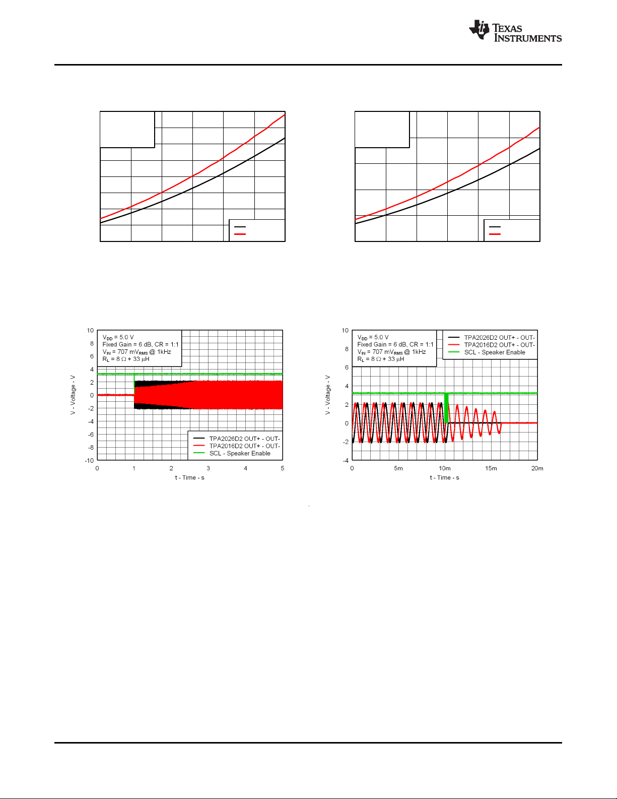
TPA2026D2 vs TPA2016D2 Startup gain ramp Figure 27
TPA2026D2 vs TPA2016D2 Shutdown gain ramp Figure 28
Shutdown time Figure 29
Startup time Figure 30
Copyright © 2010, Texas Instruments Incorporated Submit Documentation Feedback 7
Product Folder Link(s): TPA2026D2
Page 8
VDD − Supply Voltage − V
0
2
4
6
8
10
2.5 3.5 4.5 5.5
I
DD
− Quiescent Supply Current − mA
G001
VDD − Supply Voltage − V
0
20
40
60
80
100
2.5 3.5 4.5 5.5
I
DD
− Supply Current − µA
G002
SDZ = 0 V
SDZ = VDD, SWS = 1
Input Level − dBV
−50
−40
−30
−20
−10
0
10
20
−40 −30 −20 −10 0 10
Output Level − dBV
G003
RL = 8 Ω + 33 µH
V
Supply
= 5 V
Fixed Gain = Max Gain = 30 dB
Compression Ratio = 1:1
Limiter Level = −6.5
Limiter Level = −4.5
Limiter Level = −2.5
Limiter Level = −0.5
Limiter Level = 1.5
Limiter Level = 3.5
Limiter Level = 5.5
Limiter Level = 7.5
Limiter Level = 9
Input Level − dBV
−50
−40
−30
−20
−10
0
10
20
−70 −50 −30 −10 10
Output Level − dBV
G004
Limiter Level = 9 dBV
RL = 8 Ω + 33 µH
V
Supply
= 5 V
Fixed Gain (2:1)
Compression Ratio = 2:1
Max Gain = 30 dB
Fixed Gain = −12
Fixed Gain = −9
Fixed Gain = −6
Fixed Gain = −3
Fixed Gain = 0
Fixed Gain = 3
Fixed Gain = 6
Fixed Gain = 9
Fixed Gain = 12
TPA2026D2
SLOS649 –MARCH 2010
QUIESCENT SUPPLY CURRENT SUPPLY CURRENT
INPUT LEVEL WITH LIMITER ENABLED INPUT LEVEL WITH 2:1 COMPRESSION
www.ti.com
vs vs
SUPPLY VOLTAGE SUPPLY VOLTAGE IN SHUTDOWN
Figure 3. Figure 4.
OUTPUT LEVEL OUTPUT LEVEL
vs vs
Figure 5. Figure 6.
8 Submit Documentation Feedback Copyright © 2010, Texas Instruments Incorporated
Product Folder Link(s): TPA2026D2
Page 9
Input Level − dBV
−50
−40
−30
−20
−10
0
10
20
−70 −50 −30 −10 10
Output Level − dBV
G005
Limiter Level = 9 dBV
RL = 8 Ω + 33 µH
V
Supply
= 5 V
Compression Ratio = 4:1
Max Gain = 30 dB
Fixed Gain = −15
Fixed Gain = −12
Fixed Gain = −9
Fixed Gain = −6
Fixed Gain = −3
Fixed Gain = 0
Fixed Gain = 3
Fixed Gain = 6
Fixed Gain = −27
Fixed Gain = −24
Fixed Gain = −21
Fixed Gain = −18
Input Level − dBV
−50
−40
−30
−20
−10
0
10
20
−70 −50 −30 −10 10
Output Level − dBV
G006
Limiter Level = 9 dBV
RL = 8 Ω + 33 µH
V
Supply
= 5 V
Compression Ratio = 8:1
Max Gain = 30 dB
Fixed Gain = −12
Fixed Gain = −9
Fixed Gain = −6
Fixed Gain = −3
Fixed Gain = 0
Fixed Gain = 3
Fixed Gain = −27
Fixed Gain = −24
Fixed Gain = −21
Fixed Gain = −18
Fixed Gain = −15
f − Frequency − Hz
K
SVR
− Supply Ripple Rejection Ratio − dB
20 100 1k 10k 20k
−100
−80
−60
−40
−20
0
V
Supply
= 2.5 V
V
Supply
= 3.6 V
V
Supply
= 5.0 V
Gain = 6 dB
RL = 8 Ω + 33 µH
Left Channel
Input Level − dBV
−50
−40
−30
−20
−10
0
10
20
−70 −50 −30 −10 10
Output Level − dBV
G007
Compression Ratio = 1:1
Compression Ratio = 2:1
Compression Ratio = 4:1
Compression Ratio = 8:1
Limiter Level = 9 dBV
RL = 8 Ω + 33 µH
V
Supply
= 5 V
Fixed Gain = 0 dB
Max Gain = 30 dB
f − Frequency − Hz
THD+N − Total Harmonic Distortion + Noise − %
20 100 1k 10k 20k
0.001
0.01
0.1
1
10
PO = 25 mW
PO = 125 mW
PO = 300 mW
Gain = 6 dB
RL = 4 Ω + 33 µH
V
Supply
= 2.5 V
f − Frequency − Hz
THD+N − Total Harmonic Distortion + Noise − %
20 100 1k 10k 20k
0.001
0.01
0.1
1
10
PO = 25 mW
PO = 125 mW
PO = 200 mW
Gain = 6 dB
RL = 8 Ω + 33 µH
V
Supply
= 2.5 V
TPA2026D2
www.ti.com
SLOS649 –MARCH 2010
OUTPUT LEVEL OUTPUT LEVEL
vs vs
INPUT LEVEL WITH 4:1 COMPRESSION INPUT LEVEL WITH 8:1 COMPRESSION
Figure 7. Figure 8.
OUTPUT LEVEL SUPPLY RIPPLE REJECTION RATIO
vs vs
INPUT LEVEL FREQUENCY, 8Ω
Figure 9. Figure 10.
TOTAL HARMONIC DISTORTION + NOISE TOTAL HARMONIC DISTORTION + NOISE
FREQUENCY Vsupply = 2.5V, 4Ω FREQUENCY Vsupply = 2.5V, 8Ω
Copyright © 2010, Texas Instruments Incorporated Submit Documentation Feedback 9
Figure 11. Figure 12.
vs vs
Product Folder Link(s): TPA2026D2
Page 10
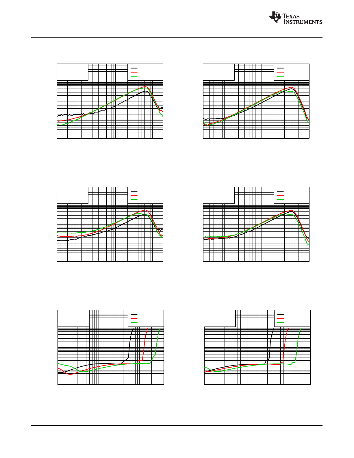
f − Frequency − Hz
THD+N − Total Harmonic Distortion + Noise − %
20 100 1k 10k 20k
0.001
0.01
0.1
1
10
PO = 50 mW
PO = 250 mW
PO = 700 mW
Gain = 6 dB
RL = 4 Ω + 33 µH
V
Supply
= 3.6 V
f − Frequency − Hz
THD+N − Total Harmonic Distortion + Noise − %
20 100 1k 10k 20k
0.001
0.01
0.1
1
10
PO = 50 mW
PO = 250 mW
PO = 500 mW
Gain = 6 dB
RL = 8 Ω + 33 µH
V
Supply
= 3.6 V
f − Frequency − Hz
THD+N − Total Harmonic Distortion + Noise − %
20 100 1k 10k 20k
0.001
0.01
0.1
1
10
PO = 100 mW
PO = 500 mW
PO = 1.75 W
Gain = 6 dB
RL = 4 Ω + 33 µH
V
Supply
= 5.0 V
f − Frequency − Hz
THD+N − Total Harmonic Distortion + Noise − %
20 100 1k 10k 20k
0.001
0.01
0.1
1
10
PO = 100 mW
PO = 500 mW
PO = 1 W
Gain = 6 dB
RL = 8 Ω + 33 µH
V
Supply
= 5.0 V
PO − Output Power (Per Channel) − W
THD+N − Total Harmonic Distortion + Noise − %
10m 100m 1 4
0.01
0.1
1
10
100
V
Supply
= 2.5 V
V
Supply
= 3.6 V
V
Supply
= 5.0 V
Gain = 6 dB
RL = 4 Ω + 33 µH
f = 1 kHz
PO − Output Power (Per Channel) − W
THD+N − Total Harmonic Distortion + Noise − %
10m 100m 1 3
0.01
0.1
1
10
100
V
Supply
= 2.5 V
V
Supply
= 3.6 V
V
Supply
= 5.0 V
Gain = 6 dB
RL = 8 Ω + 33 µH
f = 1 kHz
TPA2026D2
SLOS649 –MARCH 2010
TOTAL HARMONIC DISTORTION + NOISE TOTAL HARMONIC DISTORTION + NOISE
FREQUENCY Vsupply = 3.6V, 4Ω FREQUENCY Vsupply = 3.6V, 8Ω
TOTAL HARMONIC DISTORTION + NOISE TOTAL HARMONIC DISTORTION + NOISE
FREQUENCY Vsupply = 5.0V, 4Ω FREQUENCY Vsupply = 5.0V, 8Ω
www.ti.com
vs vs
Figure 13. Figure 14.
vs vs
Figure 15. Figure 16.
TOTAL HARMONIC DISTORTION + NOISE TOTAL HARMONIC DISTORTION + NOISE
POWER, 4Ω POWER, 8Ω
Figure 17. Figure 18.
10 Submit Documentation Feedback Copyright © 2010, Texas Instruments Incorporated
vs vs
Product Folder Link(s): TPA2026D2
Page 11
PO − Output Power (Per Channel) − W
Efficiency − %
0.0 0.5 1.0 1.5 2.0 2.5 3.0 3.5
0
20
40
60
80
100
V
Supply
= 2.5 V
V
Supply
= 3.6 V
V
Supply
= 5.0 V
Gain = 6 dB
RL = 4 Ω + 33 µH
f = 1 kHz
PO − Output Power (Per Channel) − W
Efficiency − %
0.0 0.5 1.0 1.5 2.0
0
20
40
60
80
100
V
Supply
= 2.5 V
V
Supply
= 3.6 V
V
Supply
= 5.0 V
Gain = 6 dB
RL = 8 Ω + 33 µH
f = 1 kHz
PO − Total Output Power − W
P
D
− Total Power Dissipation − W
0 1 2 3 4 5 6 7
0.0
0.1
0.2
0.3
0.4
0.5
0.6
0.7
0.8
0.9
1.0
V
Supply
= 2.5 V
V
Supply
= 3.6 V
V
Supply
= 5.0 V
Gain = 6 dB
RL = 4 Ω + 33 µH
f = 1 kHz
PO − Total Output Power − W
P
D
− Total Power Dissipation − W
0 1 2 3 4
0.0
0.1
0.2
0.3
0.4
V
Supply
= 2.5 V
V
Supply
= 3.6 V
V
Supply
= 5.0 V
Gain = 6 dB
RL = 8 Ω + 33 µH
f = 1 kHz
PO − Total Output Power − W
I
DD
− Total Supply Current − A
0 1 2 3 4 5 6 7
0.0
0.2
0.4
0.6
0.8
1.0
1.2
1.4
1.6
V
Supply
= 2.5 V
V
Supply
= 3.6V
V
Supply
= 5.0 V
Gain = 6 dB
RL = 4 Ω + 33 µH
f = 1 kHz
PO − Total Output Power − W
I
DD
− Total Supply Current − A
0 1 2 3 4
0.0
0.2
0.4
0.6
0.8
1.0
V
Supply
= 2.5 V
V
Supply
= 3.6V
V
Supply
= 5.0 V
Gain = 6 dB
RL = 8 Ω + 33 µH
f = 1 kHz
TPA2026D2
www.ti.com
SLOS649 –MARCH 2010
EFFICIENCY EFFICIENCY
vs vs
OUTPUT POWER (PER CHANNEL), 4Ω OUTPUT POWER (PER CHANNEL), 8Ω
Figure 19. Figure 20.
TOTAL POWER DISSIPATION TOTAL POWER DISSIPATION
vs vs
TOTAL OUTPUT POWER, 4Ω TOTAL OUTPUT POWER, 8Ω
Figure 21. Figure 22.
TOTAL SUPPLY CURRENT TOTAL SUPPLY CURRENT
TOTAL OUTPUT POWER, 4Ω TOTAL OUTPUT POWER, 8Ω
Copyright © 2010, Texas Instruments Incorporated Submit Documentation Feedback 11
Figure 23. Figure 24.
vs vs
Product Folder Link(s): TPA2026D2
Page 12
Vsupply − Supply Voltage − V
P
O
− Output Power − W
2.5 3.0 3.5 4.0 4.5 5.0 5.5
0.0
0.5
1.0
1.5
2.0
2.5
3.0
3.5
4.0
THD = 1%
THD = 10%
f = 1 kHz
Gain = 6 dB
RL = 4 Ω + 33 µH
WCSP
Vsupply − Supply Voltage − V
P
O
− Output Power − W
2.5 3.0 3.5 4.0 4.5 5.0 5.5
0.0
0.5
1.0
1.5
2.0
2.5
THD = 1%
THD = 10%
f = 1 kHz
Gain = 6 dB
RL = 8 Ω + 33 µH
WCSP
TPA2026D2
SLOS649 –MARCH 2010
TPA2016D2 STARTUP GAIN RAMP TPA2016D2 SHUTDOWN GAIN RAMP
www.ti.com
OUTPUT POWER OUTPUT POWER
vs vs
SUPPLY VOLTAGE, 4Ω SUPPLY VOLTAGE, 8Ω
Figure 25. Figure 26.
TPA2026D2 TPA2026D2
vs vs
Figure 27. Figure 28.
12 Submit Documentation Feedback Copyright © 2010, Texas Instruments Incorporated
Product Folder Link(s): TPA2026D2
Page 13

1
0.5
0.75
0.25
0
-0.25
-0.5
-0.75
-1
0 400m200m 600m 800m 1m 1.2m 1.6m1.4m 1.8m 2m
t-Time-s
Voltage-V
Output
SWS
Disable
1
0.5
0.75
0.25
0
-0.25
-0.5
-0.75
-1
0 2m1m 3m 4m 5m 6m 8m7m 9m 10m
t-Time-s
Voltage-V
Output
SWSEnable
TPA2026D2
www.ti.com
SLOS649 –MARCH 2010
Figure 29. Shutdown Time
Figure 30. Startup Time
Copyright © 2010, Texas Instruments Incorporated Submit Documentation Feedback 13
Product Folder Link(s): TPA2026D2
Page 14

TPA2026D2
SLOS649 –MARCH 2010
www.ti.com
APPLICATION INFORMATION
AUTOMATIC GAIN CONTROL
The Automatic Gain Control (AGC) feature provides continuous automatic gain adjustment to the amplifier
through an internal PGA. This feature enhances the perceived audio loudness and at the same time prevents
speaker damage from occurring (Limiter function).
The AGC function attempts to maintain the audio signal gain as selected by the user through the Fixed Gain,
Limiter Level, and Compression Ratio variables. Other advanced features included are Maximum Gain and Noise
Gate Threshold. Table 1 describes the function of each variable in the AGC function.
Table 1. TPA2026D2 AGC Variable Descriptions
VARIABLE DESCRIPTION
Maximum Gain The gain at the lower end of the compression region.
Fixed Gain The normal gain of the device when the AGC is inactive.
The fixed gain is also the initial gain when the device comes out of shutdown mode or when the AGC is
disabled.
Limiter Level The value that sets the maximum allowed output amplitude.
Compression Ratio The relation between input and output voltage.
Noise Gate Threshold Below this value, the AGC holds the gain to prevent breathing effects.
Attack Time The minimum time between two gain decrements.
Release Time The minimum time between two gain increments.
Hold Time The time it takes for the very first gain increment after the input signal amplitude decreases.
14 Submit Documentation Feedback Copyright © 2010, Texas Instruments Incorporated
Product Folder Link(s): TPA2026D2
Page 15

ReleaseTime
E
Limiterthreshold
GAIN
A
C
B
D
AttackTime
Limiterthreshold
Limiterthreshold
HoldTime
INPUTSIGNAL
OUTPUTSIGNAL
Limiterthreshold
TPA2026D2
www.ti.com
SLOS649 –MARCH 2010
The AGC works by detecting the audio input envelope. The gain changes depending on the amplitude, the limiter
level, the compression ratio, and the attack and release time. The gain changes constantly as the audio signal
increases and/or decreases to create the compression effect. The gain step size for the AGC is 0.5 dB. If the
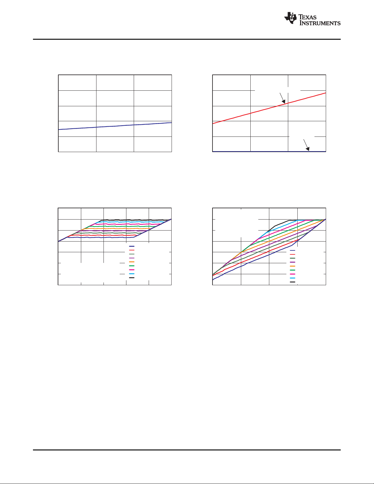
audio signal has near-constant amplitude, the gain does not change. Figure 31 shows how the AGC works.
A. Gain decreases with no delay; attack time is reset. Release time and hold time are reset.
B. Signal amplitude above limiter level, but gain cannot change because attack time is not over.
C. Attack time ends; gain is allowed to decrease from this point forward by one step. Gain decreases because the
amplitude remains above limiter threshold. All times are reset
D. Gain increases after release time finishes and signal amplitude remains below desired level. All times are reset after
the gain increase.
E. Gain increases after release time is finished again because signal amplitude remains below desired level. All times
are reset after the gain increase.
Figure 31. Input and Output Audio Signal vs Time
Since the number of gain steps is limited the compression region is limited as well. The following figure shows
how the gain changes vs. the input signal amplitude in the compression region.
Copyright © 2010, Texas Instruments Incorporated Submit Documentation Feedback 15
Product Folder Link(s): TPA2026D2
Page 16

Gain-dB
V -dBV
IN
V -dBV
OUT
V -dBV
IN
Increasing
FixedGain
Decreasing
FixedGain
FixedGain=6dB
FixedGain=3dB
1:1
TPA2026D2
SLOS649 –MARCH 2010
www.ti.com
Figure 32. Input Signal Voltage vs Gain
Thus the AGC performs a mapping of the input signal vs. the output signal amplitude. This mapping can be
modified according to the variables from Table 1.
The following graphs and explanations show the effect of each variable to the AGC independently and which
considerations should be taken when choosing values.
Fixed Gain: The fixed gain determines the initial gain of the AGC. Set the gain using the following variables:
• Set the fixed gain to be equal to the gain when the AGC is disabled.
• Set the fixed gain to maximize SNR.
• Set the fixed gain such that it will not overdrive the speaker.
Figure 33 shows how the fixed gain influences the input signal amplitude vs. the output signal amplitude state
diagram. The dotted 1:1 line is displayed for reference. The 1:1 line means that for a 1dB increase in the input
signal, the output increases by 1dB.
Figure 33. Output Signal vs Input Signal State Diagram Showing Different Fixed Gain Configurations
If the Compression function is enabled, the Fixed Gain is adjustable from –28dB to 30dB. If the Compression
function is disabled, the Fixed gain is adjustable from 0dB to 30dB.
Limiter Level: The Limiter level sets the maximum amplitude allowed at the output of the amplifier. The limiter
should be set with the following constraints in mind:
• Below or at the maximum power rating of the speaker
• Below the minimum supply voltage in order to avoid clipping
Figure 34 shows how the limiter level influences the input signal amplitude vs. the output signal amplitude state
diagram.
16 Submit Documentation Feedback Copyright © 2010, Texas Instruments Incorporated
Product Folder Link(s): TPA2026D2
Page 17

V -dBV
OUT
V -dBV
IN
Increasing
Limiter
Level
Decreasing
Limiter
Level
LimiterLevel= 500 mW
LimiterLevel= 630 mW
= 400LimiterLevel mW
V -dBV
OUT
V -dBV
IN
1:1
LargeFixedGain
Small
Fixed
Gain
Input signal initial amplitude - |Current input signal amplitude|
Output signal amplitude =
Compression ratio
0dBV | 32 dBV|
8dBV =
4
- -
-
TPA2026D2
www.ti.com
SLOS649 –MARCH 2010
Figure 34. Output Signal vs Input Signal State Diagram Showing Different Limiter Level Configurations
The limiter level and the fixed gain influence each other. If the fixed gain is set high, the AGC has a large limiter
range. The fixed gain is set low, the AGC has a short limiter range. Figure 35 illustrates the two examples:
Figure 35. Output Signal vs Input Signal State Diagram Showing Same Limiter Level Configurations with
Compression Ratio: The compression ratio sets the relation between input and output signal outside the limiter
level region. The compression ratio compresses the dynamic range of the audio. For example if the audio source
has a dynamic range of 60dB and compression ratio of 2:1 is selected, then the output has a dynamic range of
30dB. Most small form factor speakers have small dynamic range. Compression ratio allows audio with large
dynamic range to fit into a speaker with small dynamic range.
The compression ratio also increases the loudness of the audio without increasing the peak voltage. The higher
the compression ratio, the louder the perceived audio.
For example:
• A compression ratio of 4:1 is selected (meaning that a 4dB change in the input signal results in a 1dB signal
change at the output)
• A fixed gain of 0dB is selected and the maximum audio level is at 0dBV.
When the input signal decreases to –32dBV, the amplifier increases the gain to 24dB in order to achieve an
output of –8dBV. The output signal amplitude equation is:
In this example:
Copyright © 2010, Texas Instruments Incorporated Submit Documentation Feedback 17
Different Fixed Gain Configurations
Product Folder Link(s): TPA2026D2
(1)
(2)
Page 18

1
Gain change = 1 × Input signal change
Compression ratio
æ ö
-
ç ÷
è ø
1
24 dB = 1 × 32
4
æ ö
-
ç ÷
è ø
V -dBV
OUT
V -dBV
IN
Increasing
FixedGain
Decreasing
1 :1
2
:
1
4
:
1
8
:
1
1 :1
2
:
1
4
:
1
8
:
1
Rotation
Point@
lowergain
Rotation
Point@
highergain
TPA2026D2
SLOS649 –MARCH 2010
The gain change equation is:
Consider the following when setting the compression ratio:
• Dynamic range of the speaker
• Fixed gain level
• Limiter Level
• Audio Loudness vs Output Dynamic Range.
Figure 36 shows different settings for dynamic range and different fixed gain selected but no limiter level.
www.ti.com
(3)
(4)
Figure 36. Output Signal vs Input Signal State Diagram Showing Different Compression Ratio
The rotation point is always at VIN= 10dBV. The rotation point is not located at the intersection of the limiter
region and the compression region. By changing the fixed gain the rotation point will move in the y-axis direction
only, as shown in the previous graph.
Interaction Between Compression Ratio and Limiter Range: The compression ratio can be limited by the
limiter range. Note that the limiter range is selected by the limiter level and the fixed gain.
For a setting with large limiter range, the amount of gain steps in the AGC remaining to perform compression are
limited. Figure 37 shows two examples, where the fixed gain was changed.
1. Small limiter range yielding a large compression region (small fixed gain).
2. Large limiter range yielding a small compression region (large fixed gain).
18 Submit Documentation Feedback Copyright © 2010, Texas Instruments Incorporated
Configurations with Different Fixed Gain Configurations
Product Folder Link(s): TPA2026D2
Page 19

V
OUT
-dBV
V - dBV
IN
1:1
Large Limiter
Range
Small
Compression
Region
Large
Compression
Region
Small Limiter
Range
Rotation
Point @
lower gain
Rotation
Point @
higher gain
time
Gain-dB
InputSignal
Amplitude-Vrms
time
NoiseGateThreshold
No
Audio
Gaindoesnotchange
inthisregion
TPA2026D2
www.ti.com
SLOS649 –MARCH 2010
Figure 37. Output Signal vs Input Signal State Diagram Showing the Effects of the Limiter Range to the
Compression Region
Noise Gate Threshold: The noise gate threshold prevents the AGC from changing the gain when there is no
audio at the input of the amplifier. The noise gate threshold stops gain changes until the input signal is above the
noise gate threshold. Select the noise gate threshold to be above the noise but below the minimum audio at the
input of the amplifier signal. A filter is needed between delta-sigma CODEC/DAC and TPA2026D2 for
effectiveness of the noise gate function. The filter eliminates the out-of-band noise from delta-sigma modulation
and keeps the CODEC/DAC output noise lower than the noise gate threshold.
Figure 38. Time Diagram Showing the Relationship Between Input Signal Amplitude, Noise Gate
Maximum Gain: This variable limits the number of gain steps in the AGC. This feature is useful in order to
accomplish a more advanced output signal vs. input signal transfer characteristic.
For example, to prevent the gain from going above a certain value, reduce the maximum gain.
However, this variable will affect the limiter range and the compression region. If the maximum gain is
decreased, the limiter range and/or compression region is reduced. Figure 39 illustrates the effects.
Copyright © 2010, Texas Instruments Incorporated Submit Documentation Feedback 19
Threshold, and Gain Versus Time
Product Folder Link(s): TPA2026D2
Page 20

V -dBV
OUT
V -dBV
IN
MaxGain
= 22dB
MaxGain
= 30dB
1:1
TPA2026D2
SLOS649 –MARCH 2010
www.ti.com
Figure 39. Output Signal vs Input Signal State Diagram Showing Different Maximum Gains
A particular application requiring maximum gain of 22dB, for example. Thus, set the maximum gain at 22dB. The
amplifier gain will never have a gain higher than 22dB; however, this will reduce the limiter range.
Attack, Release, and Hold Time:
• The attack time is the minimum time between gain decreases.
• The release time is the minimum time between gain increases.
• The hold time is the minimum time between a gain decrease (attack) and a gain increase (release). The hold
time can be deactivated. Hold time is only valid if greater than release time.
Successive gain decreases are never faster than the attack time. Successive gain increases are never faster
than the release time.
All time variables (attack, release and hold) start counting after each gain change performed by the AGC. The
AGC is allowed to decrease the gain (attack) only after the attack time finishes. The AGC is allowed to increase
the gain (release) only after the release time finishes counting. However, if the preceding gain change was an
attack (gain increase) and the hold time is enabled and longer than the release time, then the gain is only
increased after the hold time.
The hold time is only enabled after a gain decrease (attack). The hold time replaces the release time after a gain
decrease (attack). If the gain needs to be increased further, then the release time is used. The release time is
used instead of the hold time if the hold time is disabled.
The attack time should be at least 100 times shorter than the release and hold time. The hold time should be the
same or greater than the release time. It is important to select reasonable values for those variables in order to
prevent the gain from changing too often or too slow.
Figure 40 illustrates the relationship between the three time variables.
20 Submit Documentation Feedback Copyright © 2010, Texas Instruments Incorporated
Product Folder Link(s): TPA2026D2
Page 21

InputSignal
Amplitue(Vrms)
GaindB
Attacktime
Releasetime
Timereset
Timeend
Holdtime
time
Holdtimernotusedafter
firstgainincrease
1
:
1
2:1
1:1
Noise Gate Threshold
Maximum
Gain
Fixed
Gain
Limiter
Level
Compression Region
Attack Time
R
e
l
e
a
s
e
T
im
e
4:1
8:1
10dBV
Rotation
Point
V
OUT
-dBV
V - dBV
IN
¥:1
TPA2026D2
www.ti.com
SLOS649 –MARCH 2010
Figure 40. Time Diagram Showing the Relation Between the Attack, Release, and Hold Time vs Input
Signal Amplitude and Gain
Figure 41 shows a state diagram of the input signal amplitude vs. the output signal amplitude and a summary of
how the variables from Table 1 described in the preceding pages affect them.
Copyright © 2010, Texas Instruments Incorporated Submit Documentation Feedback 21
Figure 41. Output Signal vs Input Signal State Diagram
Product Folder Link(s): TPA2026D2
Page 22

TPA2026D2
SLOS649 –MARCH 2010
www.ti.com
TPA2026D2 AGC OPERATION
The TPA2026D2 is controlled by the I2C interface. The correct start-up sequence is:
1. Apply the supply voltage to the AVDDand PVDD(L, R) pins.
2. Apply a voltage above VIHto the SDZ pin. The TPA2026D2 powers up the I2C interface and the control logic.
By default, the device is in active mode (SWS = 0). After 5 ms the amplifier will enable the class-D output
stage and become fully operational.
AGC STARTUP CONDITION
The amplifier gain at start-up depends on the following conditions:
1. Start-up from hardware reset (EN from 0 to 1): The amplifier starts up immediately at default fixed gain. AGC
starts controlling gain once the input audio signal exceeds noise gate threshold.
2. Start-up from software shutdown (SWS from 1 to 0): The amplifier starts up immediately at the latest fixed
gain during software shutdown, regardless the attack/ release time. For example:
– Audio is playing at fixed gain 6dB
– Devices goes to software shutdown (SWS = 1)
– Set fixed gain from 6 dB to 12 dB
– Remove software shutdown (SWS = 0)
– Amplifier starts up immediately at 12 dB
3. During audio playback with AGC on, gain changes according to attack/ release time. For example:
– Audio is playing at fixed gain 6 dB and 1:1 compression ratio
– Set fixed gain from 6 dB to 12 dB, at release time 500 ms / 6 dB
– Amplifier will take 500 ms to ramp from 6 dB to 12 dB
4. When SPKR_EN_R = 0, SPKR_EN_L = 0 and SWS = 0, the amplifier is set at fixed gain. The amplifier will
start up at fixed gain when either SPKR_EN_R and SPKR_EN_L transitions from 0 to 1.
CAUTION
Do not interrupt the start-up sequence after changing SDZ from VILto VIH.
Do not interrupt the start-up sequence after changing SWS from 1 to 0.
The default conditions of TPA2026D2 allows audio playback without I2C control. Refer to Table 4 for the entire
default conditions.
There are several options to disable the amplifier:
• Write SPK_EN_R = 0 and SPK_EN_L = 0 to the register (0x01, 6 and 0x01, 7). This write disables each
speaker amplifier, but leaves all other circuits operating.
• Write SWS = 1 to the register (0x01, 5). This action disables most of the amplifier functions.
• Apply VILto SDZ. This action shuts down all the circuits and has very low quiescent current consumption.
This action resets the registers to its default values.
CAUTION
Do not interrupt the shutdown sequence after changing SDZ from VIHto VIL.
Do not interrupt the shutdown sequence after changing SWS from 0 to 1.
22 Submit Documentation Feedback Copyright © 2010, Texas Instruments Incorporated
Product Folder Link(s): TPA2026D2
Page 23

Register(N)
8-BitDatafor 8-BitDatafor
Register(N+1)
TPA2026D2
www.ti.com
SLOS649 –MARCH 2010
TPA2026D2 AGC RECOMMENDED SETTINGS
Table 2. Recommended AGC Settings for Different Types of Audio Source (VDD= 3.6 V)
AUDIO COMPRESSION ATTACK TIME RELEASE TIME HOLD TIME FIXED GAIN LIMITER LEVEL
SOURCE RATIO (ms/6 dB) (ms/6 dB) (ms) (dB) (dBV)
Pop Music 4:1 1.28 to 3.84 986 to 1640 137 6 7.5
Classical 2:1 2.56 1150 137 6 8
Jazz 2:1 5.12 to 10.2 3288 — 6 8
Rap/Hip Hop 4:1 1.28 to 3.84 1640 — 6 7.5
Rock 2:1 3.84 4110 — 6 8
Voice/News 4:1 2.56 1640 — 6 8.5
GENERAL I2C OPERATION
The I2C bus employs two signals, SDA (data) and SCL (clock), to communicate between integrated circuits in a
system. The bus transfers data serially one bit at a time. The address and data 8-bit bytes are transferred most
significant bit (MSB) first. In addition, each byte transferred on the bus is acknowledged by the receiving device
with an acknowledge bit. Each transfer operation begins with the master device driving a start condition on the
bus and ends with the master device driving a stop condition on the bus. The bus uses transitions on the data
terminal (SDA) while the clock is at logic high to indicate start and stop conditions. A high-to-low transition on
SDA indicates a start and a low-to-high transition indicates a stop. Normal data-bit transitions must occur within
the low time of the clock period. Figure 42 shows a typical sequence. The master generates the 7-bit slave
address and the read/write (R/W) bit to open communication with another device, and then waits for an
acknowledge condition. The TPA2026D2 holds SDA low during the acknowledge clock period to indicate
acknowledgment. When this acknowledgment occurs, the master transmits the next byte of the sequence. Each
device is addressed by a unique 7-bit slave address plus R/W bit (1 byte). All compatible devices share the same
signals via a bidirectional bus using a wired-AND connection.
An external pull-up resistor must be used for the SDA and SCL signals to set the logic high level for the bus.
When the bus level is 5 V, use pull-up resistors between 1 kΩ and 2 kΩ.
Figure 42. Typical I2C Sequence
There is no limit on the number of bytes that can be transmitted between start and stop conditions. When the last
word transfers, the master generates a stop condition to release the bus. A generic data transfer sequence is
shown in Figure 42.
SINGLE-AND MULTIPLE-BYTE TRANSFERS
The serial control interface supports both single-byte and multi-byte read/write operations for all registers.
During multiple-byte read operations, the TPA2026D2 responds with data, one byte at a time, starting at the
register assigned, as long as the master device continues to respond with acknowledgments.
The TPA2026D2 supports sequential I2C addressing. For write transactions, if a register is issued followed by
data for that register and all the remaining registers that follow, a sequential I2C write transaction has occurred.
For I2C sequential write transactions, the register issued then serves as the starting point, and the amount of
data subsequently transmitted, before a stop or start is transmitted, determines the number of registers written.
Copyright © 2010, Texas Instruments Incorporated Submit Documentation Feedback 23
Product Folder Link(s): TPA2026D2
Page 24

A6 A5 A4 A3 A2 A1 A0
R/W
ACK A7 A6 A5 A4 A3 A2 A1 A0 ACK D7 D6 D5 D4 D3 D2 D1 D0 ACK
Start
Condition
Stop
Condition
Acknowledge Acknowledge Acknowledge
I2CDeviceAddressand
Read/WriteBit
Register DataByte
TPA2026D2
SLOS649 –MARCH 2010
www.ti.com
SINGLE-BYTE WRITE
As Figure 43 shows, a single-byte data write transfer begins with the master device transmitting a start condition
followed by the I2C device address and the read/write bit. The read/write bit determines the direction of the data
transfer. For a write data transfer, the read/write bit must be set to '0'. After receiving the correct I2C device
address and the read/write bit, the TPA2026D2 responds with an acknowledge bit. Next, the master transmits the
register byte corresponding to the TPA2026D2 internal memory address being accessed. After receiving the
register byte, the TPA2026D2 again responds with an acknowledge bit. Next, the master device transmits the
data byte to be written to the memory address being accessed. After receiving the register byte, the TPA2026D2
again responds with an acknowledge bit. Finally, the master device transmits a stop condition to complete the
single-byte data write transfer.
Figure 43. Single-Byte Write Transfer
24 Submit Documentation Feedback Copyright © 2010, Texas Instruments Incorporated
Product Folder Link(s): TPA2026D2
Page 25

Register
A6 A5 A0 R/W ACK A7 A6 A5 A4 A0 ACK A6 A5 A0 ACK
Start
Condition
Stop
Condition
Acknowledge Acknowledge Acknowledge
I2CDeviceAddressand
Read/WriteBit
Register DataByte
D7 D6 D1 D0 ACK
I2CDeviceAddressand
Read/WriteBit
Not
Acknowledge
R/WA1 A1
RepeatStart
Condition
A6 A0 ACK
Acknowledge
I2CDeviceAddressand
Read/WriteBit
R/WA6 A0 R/W ACK A0 ACK D7 D0 ACK
Start
Condition
Stop
Condition
Acknowledge Acknowledge Acknowledge
LastDataByte
ACK
FirstDataByte
RepeatStart
Condition
Not
Acknowledge
I2CDeviceAddressand
Read/WriteBit
Register
OtherDataBytes
A7 A6 A5 D7 D0 ACK
Acknowledge
D7 D0
TPA2026D2
www.ti.com
SLOS649 –MARCH 2010
MULTIPLE-BYTE WRITE AND INCREMENTAL MULTIPLE-BYTE WRITE
A multiple-byte data write transfer is identical to a single-byte data write transfer except that multiple data bytes
are transmitted by the master device to the TPA2026D2 as shown in Figure 44. After receiving each data byte,
the TPA2026D2 responds with an acknowledge bit.
Figure 44. Multiple-Byte Write Transfer
SINGLE-BYTE READ
As Figure 45 shows, a single-byte data read transfer begins with the master device transmitting a start condition
followed by the I2C device address and the read/write bit. For the data read transfer, both a write followed by a
read are actually executed. Initially, a write is executed to transfer the address byte of the internal memory
address to be read. As a result, the read/write bit is set to a '0'.
After receiving the TPA2026D2 address and the read/write bit, the TPA2026D2 responds with an acknowledge
bit. The master then sends the internal memory address byte, after which the TPA2026D2 issues an
acknowledge bit. The master device transmits another start condition followed by the TPA2026D2 address and
the read/write bit again. This time the read/write bit is set to '1', indicating a read transfer. Next, the TPA2026D2
transmits the data byte from the memory address being read. After receiving the data byte, the master device
transmits a not-acknowledge followed by a stop condition to complete the single-byte data read transfer.
Figure 45. Single-Byte Read Transfer
MULTIPLE-BYTE READ
A multiple-byte data read transfer is identical to a single-byte data read transfer except that multiple data bytes
are transmitted by the TPA2026D2 to the master device as shown in Figure 46. With the exception of the last
data byte, the master device responds with an acknowledge bit after receiving each data byte.
Figure 46. Multiple-Byte Read Transfer
Copyright © 2010, Texas Instruments Incorporated Submit Documentation Feedback 25
Product Folder Link(s): TPA2026D2
Page 26

TPA2026D2
SLOS649 –MARCH 2010
www.ti.com
Register Map
Table 3. TPA2026D2 Register Map
REGISTER Bit7 Bit6 Bit5 Bit4 Bit3 Bit2 Bit1 Bit0
1 SPK_EN_R SPL_EN_L SWS FAULT_R FAULT_L Thermal 1 NG_EN
2 0 0 ATK_time [5] ATK_time [4] ATK_time [3] ATK_time [2] ATK_time [1] ATK_time [0]
3 0 0 REL_time [5] REL_time [4] REL_time [3] REL_time [2] REL_time [1] REL_time [0]
4 0 0 Hold_time [5] Hold_time [4] Hold_tme [3] Hold_time [2] Hold_time [1] Hold_time [0]
5 0 0 FixedGain [5] FixedGain [4] FixedGain [3] FixedGain [2] FixedGain [1] FixedGain [0]
6 Limiter Limiter Level Limiter Level
Output Output Output
Disable [3] [2]
7 Max Gain [3] Max Gain [2] Max Gain [1] Max Gain [0] 0 0
The default register map values are given in Table 4.
REGISTER 0x01 0x02 0x03 0x04 0x05 0x06 0x07
Default C2h 01h 06h 0Fh 12h 19h C0h
Any register above address 0x08 is reserved for testing and should not be written to because it may change the
function of the device. If read, these bits may assume any value.
Some of the default values can be reprogrammed through the I2C interface and written to the EEPROM. This
function is useful to speed up the turn-on time of the device and minimizes the number of I2C writes. If this is
required, contact your local TI representative.
The TPA2026D2 I2C address is 0xB0 (binary 10110000) for writing and 0xB1 (binary 10110001) for reading. If a
different I2C address is required, contact your local TI representative. See the general I2C operation section for
more details.
The following tables show the details of the registers, the default values, and the values that can be programmed
through the I2C interface.
NoiseGate NoiseGate Output Limiter Output Limiter Output Limiter
Threshold [1] Threshold [2] Level [4] Level [1] Level [0]
Compression Compression
Ratio [1] Ratio [0]
Table 4. TPA2026D2 Default Register Values
26 Submit Documentation Feedback Copyright © 2010, Texas Instruments Incorporated
Product Folder Link(s): TPA2026D2
Page 27

TPA2026D2
www.ti.com
SLOS649 –MARCH 2010
IC FUNCTION CONTROL (Address: 1)
REGISTER
ADDRESS
01 (01H) – IC 7 SPK_EN_R 1 (enabled) Enables right amplifier
Function Control
SPK_EN_R: Enable bit for the right-channel amplifier. Amplifier is active when bit is high. This function is
SPK_EN_L: Enable bit for the left-channel amplifier. Amplifier is active when bit is high. This function is
SWS: Software shutdown control. The device is in software shutdown when the bit is '1' (control, bias
FAULT_L: This bit indicates that an over-current event has occurred on the left channel with a '1'. This bit
FAULT_R: This bit indicates that an over-current event has occurred on the right channel with a '1'. This
Thermal: This bit indicates a thermal shutdown that was initiated by the hardware with a '1'. This bit is
NG_EN: Enable bit for the Noise Gate function. This function is enabled when this bit is high. This
I2C BIT LABEL DEFAULT DESCRIPTION
6 SPK_EN_L 1 (enabled) Enables left amplifier
5 SWS 0 (enabled) Shutdown IC when bit = 1
4 FAULT_R 0 Changes to a 1 when there is a short on the right channel. Reset by writing
a 0.
3 FAULT_L 0 Changes to a 1 when there is a short on the left channel. Reset by writing a
0
2 Thermal 0 Changes to a 1 when die temperature is above 150°C
1 UNUSED 1
0 NG_EN 0 (disabled) Enables Noise Gate function
gated by thermal and returns once the IC is below the threshold temperature.
gated by thermal and returns once the IC is below the threshold temperature
and oscillator are inactive). When the bit is '0' the control, bias and oscillator are enabled.
is cleared by writing a '0' to it.
bit is cleared by writing a '0' to it.
deglitched and latched, and can be cleared by writing a '0' to it.
function can only be enabled when the Compression ratio is not 1:1.
AGC ATTACK CONTROL (Address: 2)
REGISTER
ADDRESS
02 (02H) – 7:6 Unused 00
AGC Control
I2C BIT
5:0 ATK_time 000101 AGC Attack time (gain ramp down)
ATK_time These bits set the attack time for the AGC function. The attack time is the minimum time
Copyright © 2010, Texas Instruments Incorporated Submit Documentation Feedback 27
LABEL DEFAULT DESCRIPTION
(1.28 ms/6 dB)
000001 0.1067 ms 1.28 ms 5.76 ms
000010 0.2134 ms 2.56 ms 11.52 ms
000011 0.3201 ms 3.84 ms 17.19 ms
000100 0.4268 ms 5.12 ms 23.04 ms
111111 6.722 ms 80.66 ms 362.99 ms
Per Step Per 6 dB 90% Range
(time increases by 0.1067 ms with every step)
between gain decreases.
Product Folder Link(s): TPA2026D2
Page 28

TPA2026D2
SLOS649 –MARCH 2010
www.ti.com
AGC RELEASE CONTROL (Address: 3)
REGISTER
ADDRESS
03 (03H) – AGC 7:6 Unused 00
Release
Control
I2C BIT
5:0 REL_time 001011 AGC Release time (gain ramp down)
REL_time These bits set the release time for the AGC function. The release time is the minimum time
LABEL DEFAULT DESCRIPTION
(0.9864 sec/6 dB)
000001 0.0137 s 0.1644 s 0.7398 s
000010 0.0274 s 0.3288 s 1.4796 s
000011 0.0411 s 0.4932 s 2.2194 s
000100 0.0548 s 0.6576 s 2.9592 s
111111 0.8631 s 10.36 s 46.6 s
Per Step Per 6 dB 90% Range
(time increases by 0.0137 s with every step)
between gain increases.
AGC HOLD TIME CONTROL (Address: 4)
REGISTER
ADDRESS
04 (04H) – 7:6 Unused 00
AGC Hold
Time Control
I2C BIT
5:0 Hold_time 000000 (disabled) AGC Hold time
Hold_time These bits set the hold time for the AGC function. The hold time is the minimum time between
LABEL DEFAULT DESCRIPTION
Per Step
000000 Hold Time Disable
000001 0.0137 s
000010 0.0274 s
000011 0.0411 s
000100 0.0548 s
(time increases by 0.0137 s with every step)
111111 0.8631 s
a gain decrease (attack) and a gain increase (release). The hold time can be deactivated.
28 Submit Documentation Feedback Copyright © 2010, Texas Instruments Incorporated
Product Folder Link(s): TPA2026D2
Page 29

TPA2026D2
www.ti.com
SLOS649 –MARCH 2010
AGC FIXED GAIN CONTROL (Address: 5)
REGISTER
ADDRESS
05 (05H) – 7:6 Unused 00
AGC Fixed
Gain Control
I2C BIT
5:0 Fixed Gain 000110 (6 dB) Sets the fixed gain of the amplifier: two's complement
Fixed Gain These bits are used to select the fixed gain of the amplifier. If compression is enabled, fixed
LABEL DEFAULT DESCRIPTION
Gain
100100 –28 dB
100101 –27 dB
100110 –26 dB
(gain increases by 1 dB with every step)
111101 –3 dB
111110 –2 dB
111111 –1 dB
000000 0 dB
000001 1 dB
000010 2 dB
000011 3 dB
(gain increases by 1dB with every step)
011100 28 dB
011101 29 dB
011110 30 dB
gain is adjustable from –28dB to 30dB. If compression is disabled, fixed gain is adjustable from
0dB to 30dB.
AGC CONTROL (Address: 6)
REGISTER
ADDRESS
06 (06H) – 7 Output Limiter 0 (enable) Disables the output limiter function. Can only be disabled when the AGC compression
AGC Control Disable ratio is 1:1 (off)
I2C BIT
6:5 NoiseGate 01 (4 mV
4:0 Output Limiter 11010 (6.5 dBV) Selects the output limiter level
Output Limiter This bit disables the output limiter function when set to 1. Can only be disabled when
Disable the AGC compression ratio is 1:1
NoiseGate Threshold These bits set the threshold level of the noise gate. NoiseGate Threshold is only
Output Limiter Level These bits select the output limiter level. Output Power numbers are for 8Ω load.
LABEL DEFAULT DESCRIPTION
) Select the threshold of the noise gate
Threshold
Level
rms
Output Power (Wrms) Peak Output Voltage
00000 0.03 0.67 –6.5
00001 0.03 0.71 –6
00010 0.04 0.75 –5.5
(Limiter level increases by 0.5dB with every step)
11101 0.79 3.55 8
11110 0.88 3.76 8.5
11111 0.99 3.99 9
functional when the compression ratio is not 1:1
Threshold
00 1 mV
01 4 mV
10 10 mV
11 20 mV
(Vp)
rms
rms
rms
rms
dBV
Copyright © 2010, Texas Instruments Incorporated Submit Documentation Feedback 29
Product Folder Link(s): TPA2026D2
Page 30

TPA2026D2
SLOS649 –MARCH 2010
www.ti.com
AGC CONTROL (Address: 7)
REGISTER
ADDRESS
07 (07H) – 7:4 Max Gain 1100 (30 dB) Selects the maximum gain the AGC can achieve
AGC Control
I2C BIT
3:2 Unused 00
1:0 Compression 10 (4:1) Selects the compression ratio of the AGC
Compression Ratio These bits select the compression ratio. Output Limiter is enabled by default when the
Max Gain These bits select the maximum gain of the amplifier. In order to maximize the use of the
LABEL DEFAULT DESCRIPTION
(gain increases by 1 dB with every step)
Ratio
compression ratio is not 1:1.
AGC, set the Max Gain to 30dB
Gain
0000 18 dB
0001 19 dB
0010 20 dB
1100 30 dB
Ratio
00 1:1 (off)
01 2:1
10 4:1
11 8:1
30 Submit Documentation Feedback Copyright © 2010, Texas Instruments Incorporated
Product Folder Link(s): TPA2026D2
Page 31

C
I I
1
f =
(2 R C )p ´ ´
I
I C
1
C =
(2 R f )p ´ ´
TPA2026D2
www.ti.com
DECOUPLING CAPACITOR C
S
SLOS649 –MARCH 2010
The TPA2026D2 is a high-performance Class-D audio amplifier that requires adequate power supply decoupling
to ensure the efficiency is high and total harmonic distortion (THD) is low. For higher frequency transients,
spikes, or digital hash on the line, a good low equivalent-series-resistance (ESR) 1-mF ceramic capacitor
(typically) placed as close as possible to the device PVDD (L, R) lead works best. Placing this decoupling
capacitor close to the TPA2026D2 is important for the efficiency of the Class-D amplifier, because any resistance
or inductance in the trace between the device and the capacitor can cause a loss in efficiency. For filtering
lower-frequency noise signals, a 4.7 mF or greater capacitor placed near the audio power amplifier would also
help, but it is not required in most applications because of the high PSRR of this device.
INPUT CAPACITORS C
I
The input capacitors and input resistors form a high-pass filter with the corner frequency, fC, determined in
Equation 5.
(5)
The value of the input capacitor is important to consider as it directly affects the bass (low frequency)
performance of the circuit. Speakers in wireless phones cannot usually respond well to low frequencies, so the
corner frequency can be set to block low frequencies in this application. Not using input capacitors can increase
output offset. Equation 6 is used to solve for the input coupling capacitance. If the corner frequency is within the
audio band, the capacitors should have a tolerance of ±10% or better, because any mismatch in capacitance
causes an impedance mismatch at the corner frequency and below.
(6)
YZH PACKAGE DIMENSIONS
The package dimensions for this YZH package are shown in the table below. See the package drawing at the
end of this data sheet for more details.
Packaged Devices D E
TPA2026D2YZH
Max = 2160µm Max = 2137µm
Min = 2100µm Min = 2077µm
BOARD LAYOUT
In making the pad size for the WCSP balls, it is recommended that the layout use non solder mask defined
(NSMD) land. With this method, the solder mask opening is made larger than the desired land area, and the
opening size is defined by the copper pad width. Figure 47 and Table 5 show the appropriate diameters for a
WCSP layout. The TPA2026D2 evaluation module (EVM) layout is shown in the next section as a layout
example.
Copyright © 2010, Texas Instruments Incorporated Submit Documentation Feedback 31
Product Folder Link(s): TPA2026D2
Page 32

TPA2026D2
SLOS649 –MARCH 2010
www.ti.com
Figure 47. Land Pattern Dimensions
Table 5. Land Pattern Dimensions
SOLDER PAD SOLDER MASK
DEFINITIONS OPENING THICKNESS THICKNESS
Non solder mask 275 mm × 275 mm Sq. (rounded
defined (NSMD) corners)
(1) Circuit traces from NSMD defined PWB lands should be 75 mm to 100 mm wide in the exposed area inside the solder mask opening.
Wider trace widths reduce device stand off and impact reliability.
(2) Best reliability results are achieved when the PWB laminate glass transition temperature is above the operating the range of the
intended application.
(3) Recommend solder paste is Type 3 or Type 4.
(4) For a PWB using a Ni/Au surface finish, the gold thickness should be less 0.5 mm to avoid a reduction in thermal fatigue performance.
(5) Solder mask thickness should be less than 20 mm on top of the copper circuit pattern
(6) Best solder stencil performance is achieved using laser cut stencils with electro polishing. Use of chemically etched stencils results in
inferior solder paste volume control.
(7) Trace routing away from WCSP device should be balanced in X and Y directions to avoid unintentional component movement due to
solder wetting forces.
COPPER PAD STENCIL
275 mm 375 mm
(+0.0, –25 mm) (+0.0, –25 mm)
(5)
COPPER STENCIL
1 oz max (32 mm) 125 mm thick
(1) (2) (3) (4)
(6) (7)
OPENING
COMPONENT LOCATION
Place all external components very close to the TPA2026D2. Placing the decoupling capacitor, CS, close to the
TPA2026D2 is important for the efficiency of the Class-D amplifier. Any resistance or inductance in the trace
between the device and the capacitor can cause a loss in efficiency.
TRACE WIDTH
Recommended trace width at the solder balls is 75 mm to 100 mm to prevent solder wicking onto wider PCB
traces. For high current pins (PVDD (L, R), PGND, and audio output pins) of the TPA2026D2, use 100-mm trace
widths at the solder balls and at least 500-mm PCB traces to ensure proper performance and output power for
the device. For the remaining signals of the TPA2026D2, use 75-mm to 100-mm trace widths at the solder balls.
The audio input pins (INR± and INL±) must run side-by-side to maximize common-mode noise cancellation.
32 Submit Documentation Feedback Copyright © 2010, Texas Instruments Incorporated
Product Folder Link(s): TPA2026D2
Page 33

100°C/W
JA DMAX
T T P C
A J
Max = Max - = 150 - 100 (0.4) = 110q °
Ferrite
ChipBead
Ferrite
ChipBead
1nF
1nF
OUTP
OUTN
TPA2026D2
www.ti.com
SLOS649 –MARCH 2010
EFFICIENCY AND THERMAL INFORMATION
The maximum ambient temperature depends on the heat-sinking ability of the PCB system. The derating factor
for the package is shown in the dissipation rating table. Converting this to qJAfor the WCSP package:
(7)
Given qJAof 100°C/W, the maximum allowable junction temperature of 150°C, and the maximum internal
dissipation of 0.4 W (0.2 W per channel) for 1.5 W per channel, 8-Ω load, 5-V supply, from Figure 15, the
maximum ambient temperature can be calculated with the following equation.
(8)
Equation 8 shows that the calculated maximum ambient temperature is 110°C at maximum power dissipation
with a 5-V supply and 8-Ω a load. The TPA2026D2 is designed with thermal protection that turns the device off
when the junction temperature surpasses 150°C to prevent damage to the IC. Also, using speakers more
resistive than 8-Ω dramatically increases the thermal performance by reducing the output current and increasing
the efficiency of the amplifier.
OPERATION WITH DACS AND CODECS
In using Class-D amplifiers with CODECs and DACs, sometimes there is an increase in the output noise floor
from the audio amplifier. This occurs when output frequencies of the CODEC/DAC mix with the Class-D
switching frequency and create sum/difference components in the audio band. The noise increase can be solved
by placing an RC low-pass filter between the CODEC/DAC and audio amplifier. The filter reduces high
frequencies that cause the problem and allows proper performance.
SHORT CIRCUIT AUTO-RECOVERY
When a short circuit event happens, the TPA2026D2 goes to low duty cycle mode and tries to reactivate itself
every 110 µs. This auto-recovery will continue until the short circuit event stops. This feature can protect the
device without affecting the device's long term reliability. FAULT bit (register 1, bit 3) still requires a write to clear.
FILTER FREE OPERATION AND FERRITE BEAD FILTERS
A ferrite bead filter can often be used if the design is failing radiated emissions without an LC filter and the
frequency sensitive circuit is greater than 1 MHz. This filter functions well for circuits that just have to pass FCC
and CE because FCC and CE only test radiated emissions greater than 30 MHz. When choosing a ferrite bead,
choose one with high impedance at high frequencies, and low impedance at low frequencies. In addition, select a
ferrite bead with adequate current rating to prevent distortion of the output signal.
Use an LC output filter if there are low frequency (< 1 MHz) EMI sensitive circuits and/or there are long leads
from amplifier to speaker. Figure 48 shows typical ferrite bead and LC output filters.
Figure 48. Typical Ferrite Bead Filter (Chip bead example: TDK: MPZ1608S221A)
Copyright © 2010, Texas Instruments Incorporated Submit Documentation Feedback 33
Product Folder Link(s): TPA2026D2
Page 34

PACKAGE OPTION ADDENDUM
www.ti.com 26-Apr-2010
PACKAGING INFORMATION
Orderable Device Status
(1)
Package
Type
Package
Drawing
Pins Package
Qty
Eco Plan
TPA2026D2YZHR ACTIVE DSBGA YZH 16 3000 Green (RoHS &
(2)
Lead/Ball Finish MSL Peak Temp
SNAGCU Level-1-260C-UNLIM
(3)
no Sb/Br)
TPA2026D2YZHT ACTIVE DSBGA YZH 16 250 Green (RoHS &
SNAGCU Level-1-260C-UNLIM
no Sb/Br)
(1)
The marketing status values are defined as follows:
ACTIVE: Product device recommended for new designs.
LIFEBUY: TI has announced that the device will be discontinued, and a lifetime-buy period is in effect.
NRND: Not recommended for new designs. Device is in production to support existing customers, but TI does not recommend using this part in
a new design.
PREVIEW: Device has been announced but is not in production. Samples may or may not be available.
OBSOLETE: TI has discontinued the production of the device.
(2)
Eco Plan - The planned eco-friendly classification: Pb-Free (RoHS), Pb-Free (RoHS Exempt), or Green (RoHS & no Sb/Br) - please check
http://www.ti.com/productcontent for the latest availability information and additional product content details.
TBD: The Pb-Free/Green conversion plan has not been defined.
Pb-Free (RoHS): TI's terms "Lead-Free" or "Pb-Free" mean semiconductor products that are compatible with the current RoHS requirements
for all 6 substances, including the requirement that lead not exceed 0.1% by weight in homogeneous materials. Where designed to be soldered
at high temperatures, TI Pb-Free products are suitable for use in specified lead-free processes.
Pb-Free (RoHS Exempt): This component has a RoHS exemption for either 1) lead-based flip-chip solder bumps used between the die and
package, or 2) lead-based die adhesive used between the die and leadframe. The component is otherwise considered Pb-Free (RoHS
compatible) as defined above.
Green (RoHS & no Sb/Br): TI defines "Green" to mean Pb-Free (RoHS compatible), and free of Bromine (Br) and Antimony (Sb) based flame
retardants (Br or Sb do not exceed 0.1% by weight in homogeneous material)
(3)
MSL, Peak Temp. -- The Moisture Sensitivity Level rating according to the JEDEC industry standard classifications, and peak solder
temperature.
Important Information and Disclaimer:The information provided on this page represents TI's knowledge and belief as of the date that it is
provided. TI bases its knowledge and belief on information provided by third parties, and makes no representation or warranty as to the
accuracy of such information. Efforts are underway to better integrate information from third parties. TI has taken and continues to take
reasonable steps to provide representative and accurate information but may not have conducted destructive testing or chemical analysis on
incoming materials and chemicals. TI and TI suppliers consider certain information to be proprietary, and thus CAS numbers and other limited
information may not be available for release.
In no event shall TI's liability arising out of such information exceed the total purchase price of the TI part(s) at issue in this document sold by TI
to Customer on an annual basis.
Addendum-Page 1
Page 35

PACKAGE MATERIALS INFORMATION
www.ti.com 20-Jul-2010
TAPE AND REEL INFORMATION
*All dimensions are nominal
Device Package
TPA2026D2YZHR DSBGA YZH 16 3000 180.0 8.4 2.35 2.35 0.81 4.0 8.0 Q1
Type
Package
Drawing
Pins SPQ Reel
Diameter
(mm)
Reel
Width
W1 (mm)
A0
(mm)B0(mm)K0(mm)P1(mm)W(mm)
Pin1
Quadrant
Pack Materials-Page 1
Page 36

PACKAGE MATERIALS INFORMATION
www.ti.com 20-Jul-2010
*All dimensions are nominal
Device Package Type Package Drawing Pins SPQ Length (mm) Width (mm) Height (mm)
TPA2026D2YZHR DSBGA YZH 16 3000 190.5 212.7 31.8
Pack Materials-Page 2
Page 37

D: Max =
2164 µm, Min =
2104 µm
E: Max =
2142 µm, Min =
2082 µm
Page 38

IMPORTANT NOTICE
Texas Instruments Incorporated and its subsidiaries (TI) reserve the right to make corrections, modifications, enhancements, improvements,
and other changes to its products and services at any time and to discontinue any product or service without notice. Customers should
obtain the latest relevant information before placing orders and should verify that such information is current and complete. All products are
sold subject to TI’s terms and conditions of sale supplied at the time of order acknowledgment.
TI warrants performance of its hardware products to the specifications applicable at the time of sale in accordance with TI’s standard
warranty. Testing and other quality control techniques are used to the extent TI deems necessary to support this warranty. Except where
mandated by government requirements, testing of all parameters of each product is not necessarily performed.
TI assumes no liability for applications assistance or customer product design. Customers are responsible for their products and
applications using TI components. To minimize the risks associated with customer products and applications, customers should provide
adequate design and operating safeguards.
TI does not warrant or represent that any license, either express or implied, is granted under any TI patent right, copyright, mask work right,
or other TI intellectual property right relating to any combination, machine, or process in which TI products or services are used. Information
published by TI regarding third-party products or services does not constitute a license from TI to use such products or services or a
warranty or endorsement thereof. Use of such information may require a license from a third party under the patents or other intellectual
property of the third party, or a license from TI under the patents or other intellectual property of TI.
Reproduction of TI information in TI data books or data sheets is permissible only if reproduction is without alteration and is accompanied
by all associated warranties, conditions, limitations, and notices. Reproduction of this information with alteration is an unfair and deceptive
business practice. TI is not responsible or liable for such altered documentation. Information of third parties may be subject to additional
restrictions.
Resale of TI products or services with statements different from or beyond the parameters stated by TI for that product or service voids all
express and any implied warranties for the associated TI product or service and is an unfair and deceptive business practice. TI is not
responsible or liable for any such statements.
TI products are not authorized for use in safety-critical applications (such as life support) where a failure of the TI product would reasonably
be expected to cause severe personal injury or death, unless officers of the parties have executed an agreement specifically governing
such use. Buyers represent that they have all necessary expertise in the safety and regulatory ramifications of their applications, and
acknowledge and agree that they are solely responsible for all legal, regulatory and safety-related requirements concerning their products
and any use of TI products in such safety-critical applications, notwithstanding any applications-related information or support that may be
provided by TI. Further, Buyers must fully indemnify TI and its representatives against any damages arising out of the use of TI products in
such safety-critical applications.
TI products are neither designed nor intended for use in military/aerospace applications or environments unless the TI products are
specifically designated by TI as military-grade or "enhanced plastic." Only products designated by TI as military-grade meet military
specifications. Buyers acknowledge and agree that any such use of TI products which TI has not designated as military-grade is solely at
the Buyer's risk, and that they are solely responsible for compliance with all legal and regulatory requirements in connection with such use.
TI products are neither designed nor intended for use in automotive applications or environments unless the specific TI products are
designated by TI as compliant with ISO/TS 16949 requirements. Buyers acknowledge and agree that, if they use any non-designated
products in automotive applications, TI will not be responsible for any failure to meet such requirements.
Following are URLs where you can obtain information on other Texas Instruments products and application solutions:
Products Applications
Amplifiers amplifier.ti.com Audio www.ti.com/audio
Data Converters dataconverter.ti.com Automotive www.ti.com/automotive
DLP® Products www.dlp.com Communications and www.ti.com/communications
DSP dsp.ti.com Computers and www.ti.com/computers
Clocks and Timers www.ti.com/clocks Consumer Electronics www.ti.com/consumer-apps
Interface interface.ti.com Energy www.ti.com/energy
Logic logic.ti.com Industrial www.ti.com/industrial
Power Mgmt power.ti.com Medical www.ti.com/medical
Microcontrollers microcontroller.ti.com Security www.ti.com/security
RFID www.ti-rfid.com Space, Avionics & www.ti.com/space-avionics-defense
RF/IF and ZigBee® Solutions www.ti.com/lprf Video and Imaging www.ti.com/video
Mailing Address: Texas Instruments, Post Office Box 655303, Dallas, Texas 75265
Copyright © 2010, Texas Instruments Incorporated
Telecom
Peripherals
Defense
Wireless www.ti.com/wireless-apps
 Loading...