

Datasheet TPA112EVM, TPA112MSOPEVM, TPA112DR, TPA112DGNR, TPA112D Datasheet (Texas Instruments)
...Page 1
Please be aware that an important notice concerning availability, standard warranty, and use in critical applications of
Texas Instruments semiconductor products and disclaimers thereto appears at the end of this data sheet.
TP A112
150-mW STEREO AUDIO POWER AMPLIFIER
SLOS212C – AUGUST 1998 – REVISED MARCH 2000
1
POST OFFICE BOX 655303 • DALLAS, TEXAS 75265
D
150-mW Stereo Output
D
Wide Range of Supply Voltages
– Fully Specified for 3.3 V and 5 V
Operation
– Operational From 2.5 V to 5.5 V
D
Thermal and Short-Circuit Protection
D
Surface Mount Packaging
– PowerP AD MSOP
– SOIC
D
Standard Operational Amplifier Pinout
description
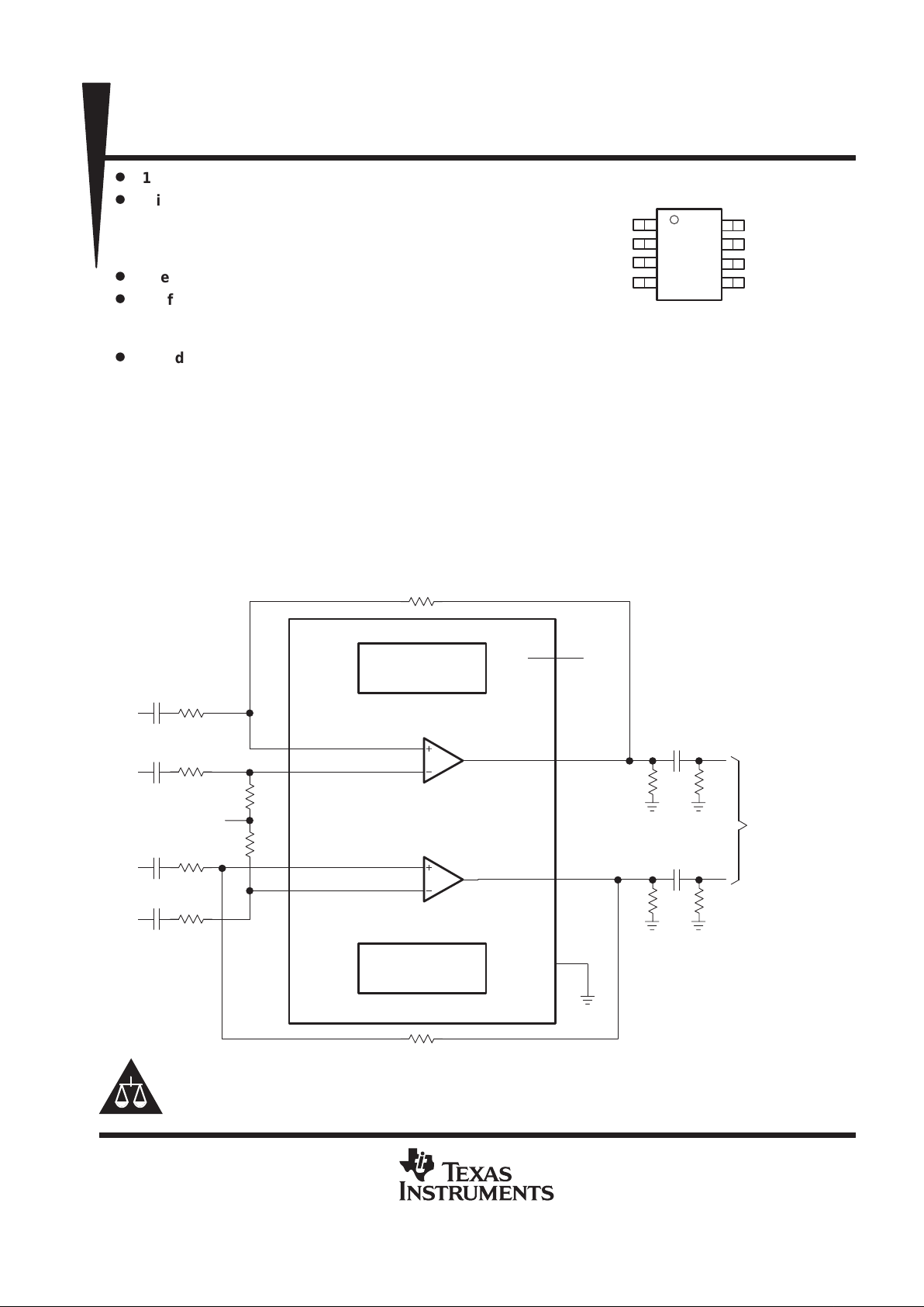
The TPA112 is a stereo audio power amplifier packaged in an 8-pin PowerPAD MSOP package capable of
delivering 150 mW of continuous RMS power per channel into 8-Ω loads. Amplifier gain is externally configured
by means of two resistors per input channel and does not require external compensation for settings of 1 to 10.
THD+N when driving an 8-Ω load from 5 V is 0.1% at 1 kHz, and less than 2% across the audio band of 20 Hz
to 20 kHz. For 32-Ω loads, the THD+N is reduced to less than 0.06% at 1 kHz, and is less than 1% across the
audio band of 20 Hz to 20 kHz. For 10-kΩ loads, the THD+N performance is 0.01% at 1 kHz, and less than 0.02%
across the audio band of 20 Hz to 20 kHz.
functional block diagram
Short-Circuit
Protection
Over-Temperature
Protection
V
DD
8
V
DD
IN1–
IN1+
IN2–
IN2+
2
3
6
5
VO1
1
VO2
7
4
R
F
R
F
R
F
R
I
R
I
R
I
R
I
V
DD/2
C
I
C
I
C
I
C
I
LIN–
LIN+
RIN–
RIN+
R
F
R
O
R
O
R
C
R
C
C
C
C
C
To Headphone
Jack
(See TPA152)
Copyright 2000, Texas Instruments Incorporated
PRODUCTION DATA information is current as of publication date.
Products conform to specifications per the terms of Texas Instruments
standard warranty. Production processing does not necessarily include
testing of all parameters.
1
2
3
4
8
7
6
5
VO1
IN1–
IN1+
GND
V
DD
VO2
IN2–
IN2+
D OR DGN PACKAGE
(TOP VIEW)
PowerPAD is a trademark of Texas Instruments.
Page 2
TPA112
150-mW STEREO AUDIO POWER AMPLIFIER
SLOS212C – AUGUST 1998 – REVISED MARCH 2000
2
POST OFFICE BOX 655303 • DALLAS, TEXAS 75265
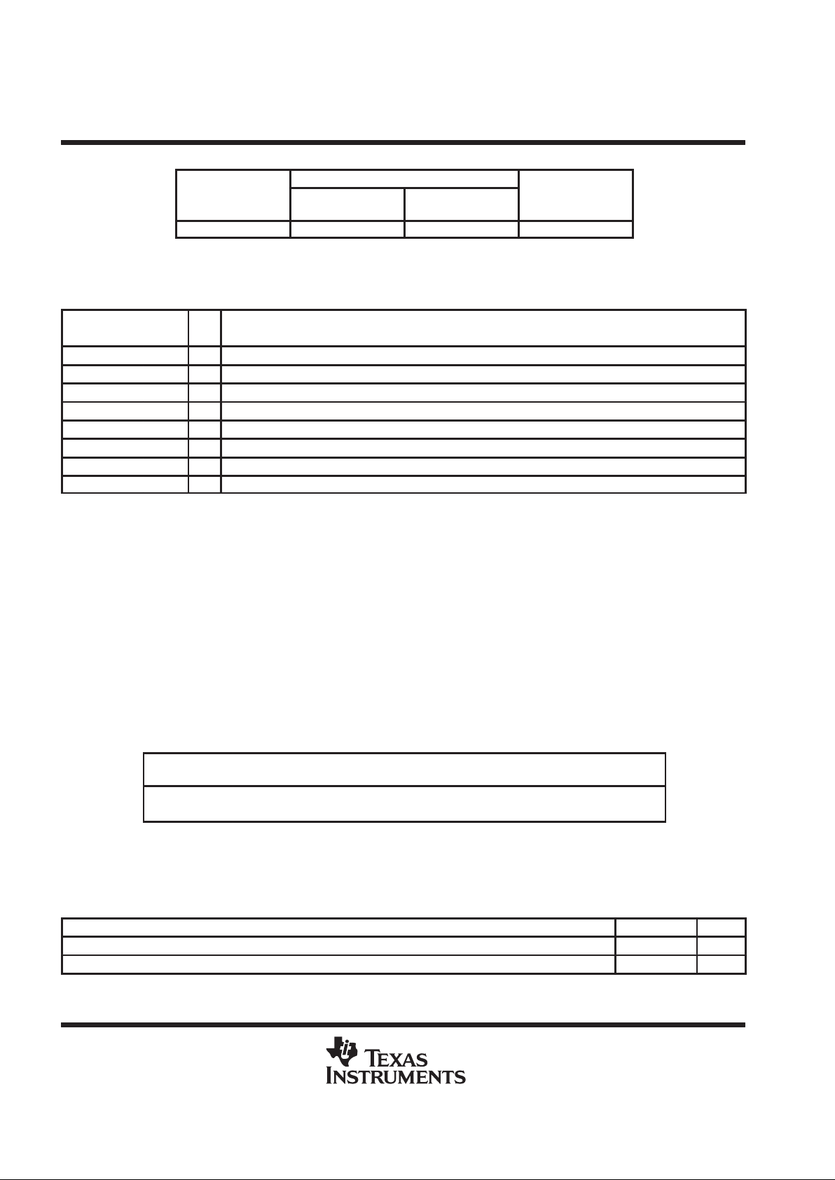
AVAILABLE OPTIONS
PACKAGED DEVICES
T
A
SMALL OUTLINE
†
(D)
MSOP
†
(DGN)
MSOP
Symbolization
–40°C to 85°C TPA112D TPA112DGN TI AAD
†
The D and DGN package is available in left-ended tape and reel only (e.g., TPA112DR,
TPA112DGNR).
Terminal Functions
TERMINAL
NAME NO.
I/O
DESCRIPTION
GND 4 I GND is the ground connection.
IN1– 2 I IN1– is the inverting input for channel 1.
IN1+ 3 I IN1+ is the noninverting input for channel 1.
IN2– 6 I IN2– is the inverting input for channel 2.
IN2+ 5 I IN2+ is the noninverting input for channel 2.
V
DD
8 I VDD is the supply voltage terminal.
VO1 1 O VO1 is the audio output for channel 1.
VO2 7 O VO2 is the audio output for channel 2.
absolute maximum ratings over operating free-air temperature (unless otherwise noted)
†
Supply voltage, VDD 6 V. . . . . . . . . . . . . . . . . . . . . . . . . . . . . . . . . . . . . . . . . . . . . . . . . . . . . . . . . . . . . . . . . . . . . . . .
Differential input voltage, VI –0.3 V to VDD + 0.3 V. . . . . . . . . . . . . . . . . . . . . . . . . . . . . . . . . . . . . . . . . . . . . . . . . .
Input current, II ±2.5 µA. . . . . . . . . . . . . . . . . . . . . . . . . . . . . . . . . . . . . . . . . . . . . . . . . . . . . . . . . . . . . . . . . . . . . . . . .
Output current, I
O
±250 mA. . . . . . . . . . . . . . . . . . . . . . . . . . . . . . . . . . . . . . . . . . . . . . . . . . . . . . . . . . . . . . . . . . . . . .
Continuous total power dissipation internally limited. . . . . . . . . . . . . . . . . . . . . . . . . . . . . . . . . . . . . . . . . . . . . . . . .
Operating junction temperature range, TJ –40°C to 150°C. . . . . . . . . . . . . . . . . . . . . . . . . . . . . . . . . . . . . . . . . . .
Storage temperature range, T
stg
–65°C to 150°C. . . . . . . . . . . . . . . . . . . . . . . . . . . . . . . . . . . . . . . . . . . . . . . . . . .
Lead temperature 1,6 mm (1/16 inch) from case for 10 seconds 260°C. . . . . . . . . . . . . . . . . . . . . . . . . . . . . . .
†
Stresses beyond those listed under “absolute maximum ratings” may cause permanent damage to the device. These are stress ratings only, and
functional operation of the device at these or any other conditions beyond those indicated under “recommended operating conditions” is not
implied. Exposure to absolute-maximum-rated conditions for extended periods may affect device reliability.
DISSIPATION RATING TABLE
PACKAGE
TA ≤ 25°C
POWER RATING
DERATING FACTOR
ABOVE TA = 25°C
TA = 70°C
POWER RATING
TA = 85°C
POWER RATING
D 725 mW 5.8 mW/°C 464 mW 377 mW
DGN 2.14 W
‡
17.1 mW/°C 1.37 W 1.11 W
‡
Please see the Texas Instruments document,
PowerPAD Thermally Enhanced Package Application Report
(literature number SLMA002), for more information on the PowerPAD package. The thermal data was
measured on a PCB layout based on the information in the section entitled
T exas Instruments Recommended
Board for PowerPAD
on page 33 of the before mentioned document.
recommended operating conditions
MIN MAX UNIT
Supply voltage, V
DD
2.5 5.5 V
Operating free-air temperature, T
A
–40 85 °C
Page 3
TPA112
150-mW STEREO AUDIO POWER AMPLIFIER
SLOS212C – AUGUST 1998 – REVISED MARCH 2000
3
POST OFFICE BOX 655303 • DALLAS, TEXAS 75265
dc electrical characteristics at TA = 25°C, VDD = 3.3 V
PARAMETER TEST CONDITIONS MIN TYP MAX UNIT
V
IO
Input offset voltage 5 mV
PSRR Power supply rejection ratio VDD = 3.2 V to 3.4 V 83 dB
I
DD(q)
Supply current 1.5 3 mA
I
DD(SD)
Supply current in SHUTDOWN mode 10 50 µA
Z
I
Input impedance >1 MΩ
ac operating characteristics, VDD= 3.3 V, TA = 25°C, RL = 8 Ω
PARAMETER TEST CONDITIONS MIN TYP MAX UNIT
P
O
Output power (each channel) THD ≤ 0.1% 70
†
mW
THD+N Total harmonic distortion + noise PO = 70 mW, 20–20 kHz 2%
B
OM
Maximum output power BW G = 10, THD <5% >20 kHz
Phase margin Open loop 58°
S
VRR
Supply ripple rejection f = 1 kHz 68 dB
Channel/channel output separation f = 1 kHz 86 dB
SNR Signal-to-noise ratio PO = 100 mW 100 dB
V
n
Noise output voltage 9.5 µV(rms)
†
Measured at 1 kHz
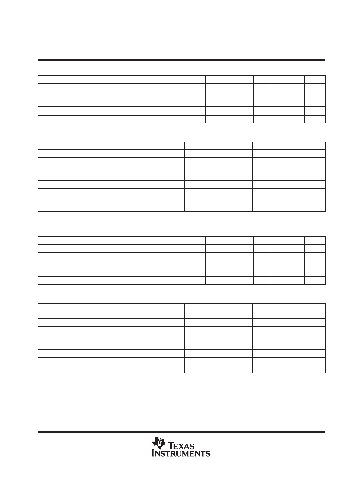
dc electrical characteristics at TA = 25°C, VDD = 5 V
PARAMETER TEST CONDITIONS MIN TYP MAX UNIT
V
IO
Input offset voltage 5 mV
PSRR Power supply rejection ratio VDD = 4.9 V to 5.1 V 76 dB
I
DD(q)
Supply current 1.5 3 mA
I
DD(SD)
Supply current in SHUTDOWN mode 60 100 µA
Z
I
Input impedance >1 MΩ
ac operating characteristics, VDD=5 V, TA = 25°C, RL = 8 Ω
PARAMETER TEST CONDITIONS MIN TYP MAX UNIT
P
O
Output power (each channel) THD ≤ 0.1% 70† mW
THD+N Total harmonic distortion + noise PO = 150 mW, 20–20 kHz 2%
B
OM
Maximum output power BW G = 10, THD <5% >20 kHz
Phase margin Open loop 56°
S
VRR
Supply ripple rejection f = 1 kHz 68 dB
Channel/channel output separation f = 1 kHz 86 dB
SNR Signal-to-noise ratio PO = 150 mW 100 dB
V
n
Noise output voltage 9.5 µV(rms)
†
Measured at 1 kHz
Page 4
TPA112
150-mW STEREO AUDIO POWER AMPLIFIER
SLOS212C – AUGUST 1998 – REVISED MARCH 2000
4
POST OFFICE BOX 655303 • DALLAS, TEXAS 75265
ac operating characteristics, VDD= 3.3 V, TA = 25°C, RL = 32 Ω
PARAMETER TEST CONDITIONS MIN TYP MAX UNIT
P
O
Output power (each channel) THD ≤ 0.1% 40
†
mW
THD+N Total harmonic distortion + noise PO = 30 mW, 20–20 kHz 0.5%
B
OM
Maximum output power BW G = 10, THD <2% >20 kHz
Phase margin Open loop 58°
S
VRR
Supply ripple rejection f = 1 kHz 68 dB
Channel/channel output separation f = 1 kHz 86 dB
SNR Signal-to-noise ratio PO = 100 mW 100 dB
V
n
Noise output voltage 9.5 µV(rms)
†
Measured at 1 kHz
ac operating characteristics, VDD=5 V, TA = 25°C, RL = 32 Ω
PARAMETER TEST CONDITIONS MIN TYP MAX UNIT
P
O
Output power (each channel) THD ≤ 0.1% 40† mW
THD+N Total harmonic distortion + noise PO = 60 mW, 20–20 kHz 0.4%
B
OM
Maximum output power BW G = 10, THD <2% >20 kHz
Phase margin Open loop 56°
S
VRR
Supply ripple rejection f = 1 kHz 68 dB
Channel/channel output separation f = 1 kHz 86 dB
SNR Signal-to-noise ratio PO = 150 mW 100 dB
V
n
Noise output voltage 9.5 µV(rms)
†
Measured at 1 kHz
Page 5
TPA112
150-mW STEREO AUDIO POWER AMPLIFIER
SLOS212C – AUGUST 1998 – REVISED MARCH 2000
5
POST OFFICE BOX 655303 • DALLAS, TEXAS 75265
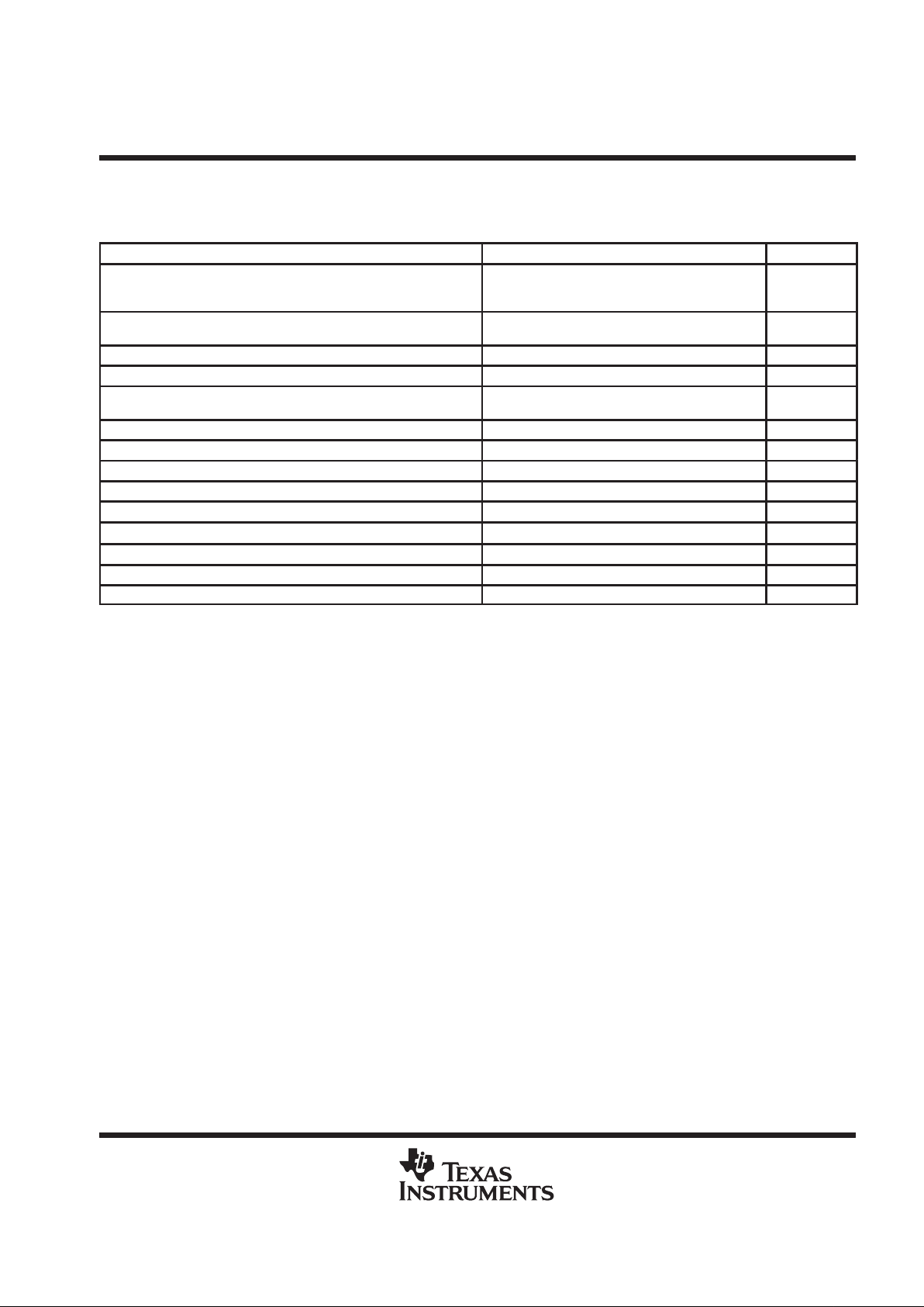
TYPICAL CHARACTERISTICS
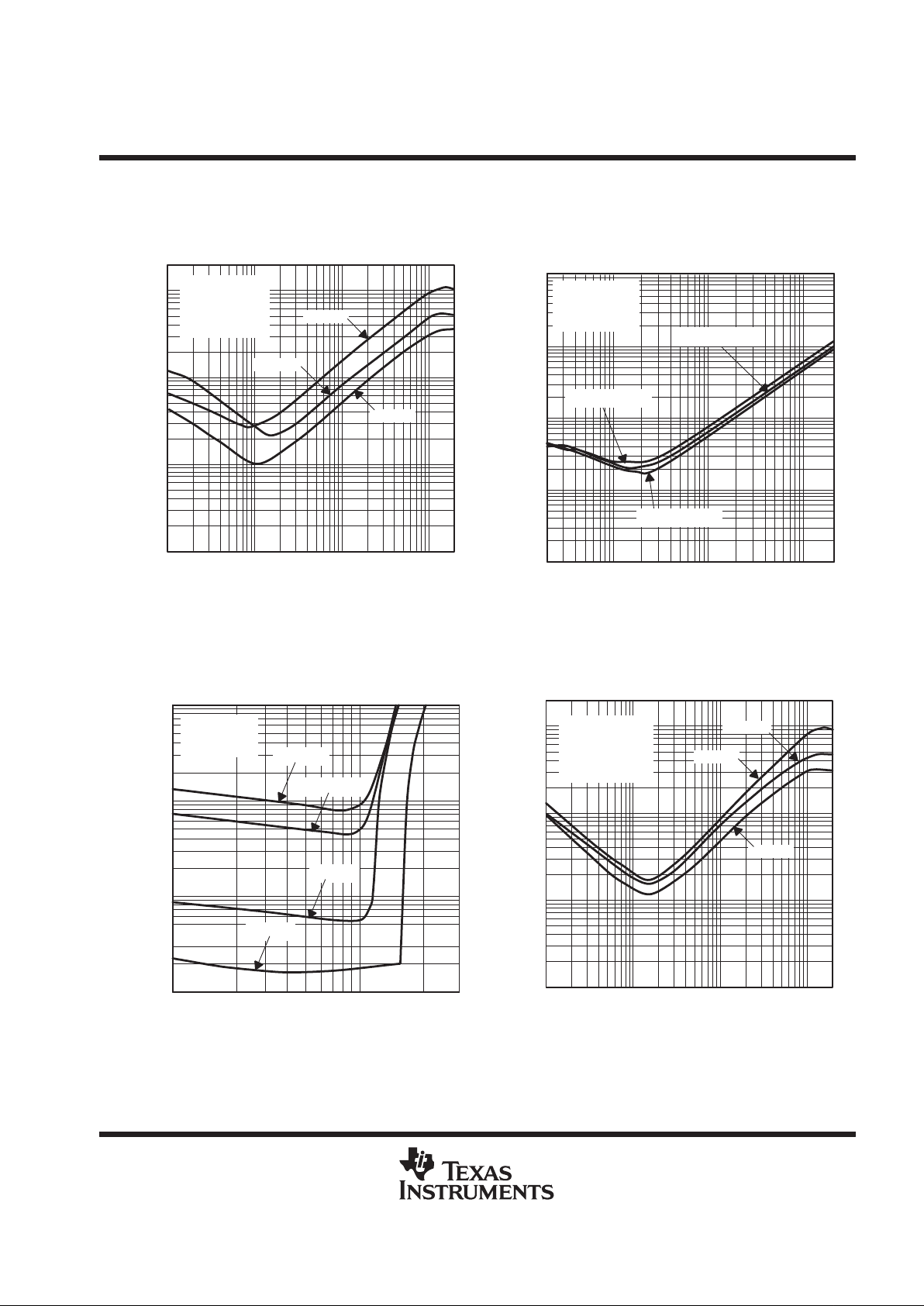
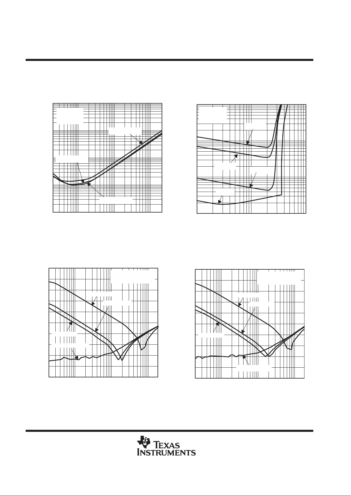
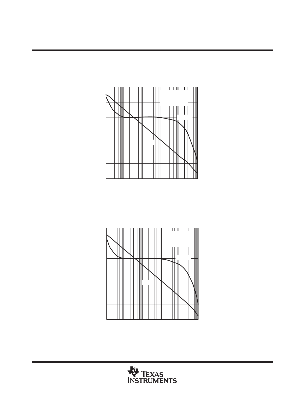
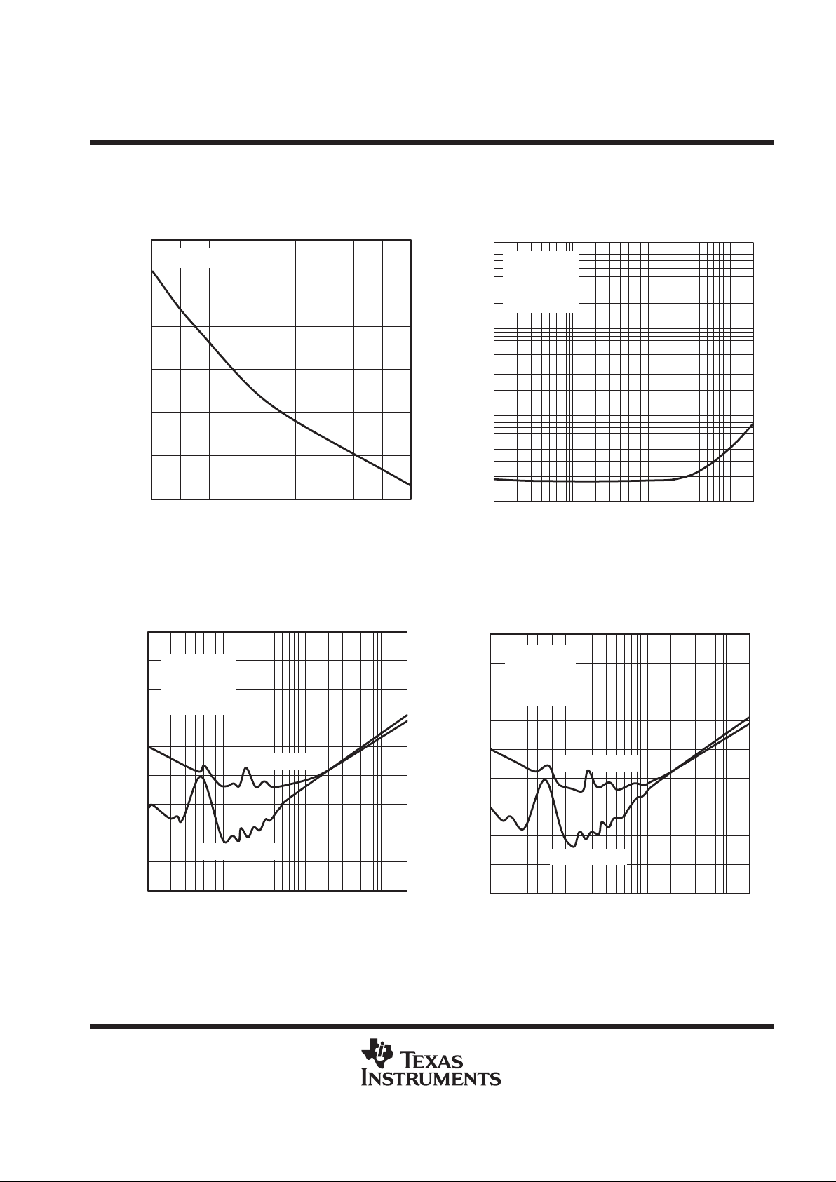
Table of Graphs
FIGURE
THD+N Total harmonic distortion plus noise vs Frequency
1, 2, 4, 5, 7, 8,
10, 11, 13, 14,
16, 17, 34, 36
vs Power output
3, 6, 9,
12, 15, 18
PSSR Power supply rejection ratio vs Frequency 19, 20
V
n
Output noise voltage vs Frequency 21, 22
Crosstalk vs Frequency
23 – 26,
37, 38
Mute attenuation vs Frequency 27, 28
Open-loop gain vs Frequency 29, 30
Phase margin vs Frequency 29, 30
Phase vs Frequency 39 – 44
Output power vs Load resistance 31, 32
I
CC
Supply current vs Supply voltage 33
SNR Signal-to-noise ratio vs Voltage gain 35
Closed-loop gain vs Frequency 39 – 44
Power dissipation/amplifier vs Output power 45, 46
Page 6
TPA112
150-mW STEREO AUDIO POWER AMPLIFIER
SLOS212C – AUGUST 1998 – REVISED MARCH 2000
6
POST OFFICE BOX 655303 • DALLAS, TEXAS 75265
TYPICAL CHARACTERISTICS
Figure 1
0.1
0.01
0.001
1
10
20 100 1k 10k 20k
TOTAL HARMONIC DISTORTION PLUS NOISE
vs
FREQUENCY
AV = 10
AV = 5
THD+N –Total Harmonic Distortion + Noise – %
f – Frequency – Hz
AV = 1
VDD = 3.3 V
PO = 30 mW
CB = 1 µ F
RL = 32 Ω
Figure 2
0.1
0.01
0.001
1
10
20 100 1k 10k 20k
TOTAL HARMONIC DISTORTION PLUS NOISE
vs
FREQUENCY
VDD = 3.3 V
AV = 1 V/V
RL = 32 Ω
CB = 1 µ F
PO = 10 mW
THD+N –Total Harmonic Distortion + Noise – %
f – Frequency – Hz
PO = 15 mW
PO = 30 mW
Figure 3
TOTAL HARMONIC DISTORTION PLUS NOISE
vs
OUTPUT POWER
10 kHz
0.1
0.01
1
10
THD+N –Total Harmonic Distortion + Noise – %
PO – Output Power – mW
11050
VDD = 3.3 V
RL = 32 Ω
AV = 1 V/V
CB = 1 µF
20 kHz
1 kHz
20 Hz
Figure 4
0.1
0.01
0.001
1
10
20 100 1k 10k 20k
TOTAL HARMONIC DISTORTION PLUS NOISE
vs
FREQUENCY
VDD = 5 V
PO = 60 mW
RL = 32 Ω
CB = 1 µF
AV = 10 mW
THD+N –Total Harmonic Distortion + Noise – %
f – Frequency – Hz
AV = 5 mW
AV = 1 mW
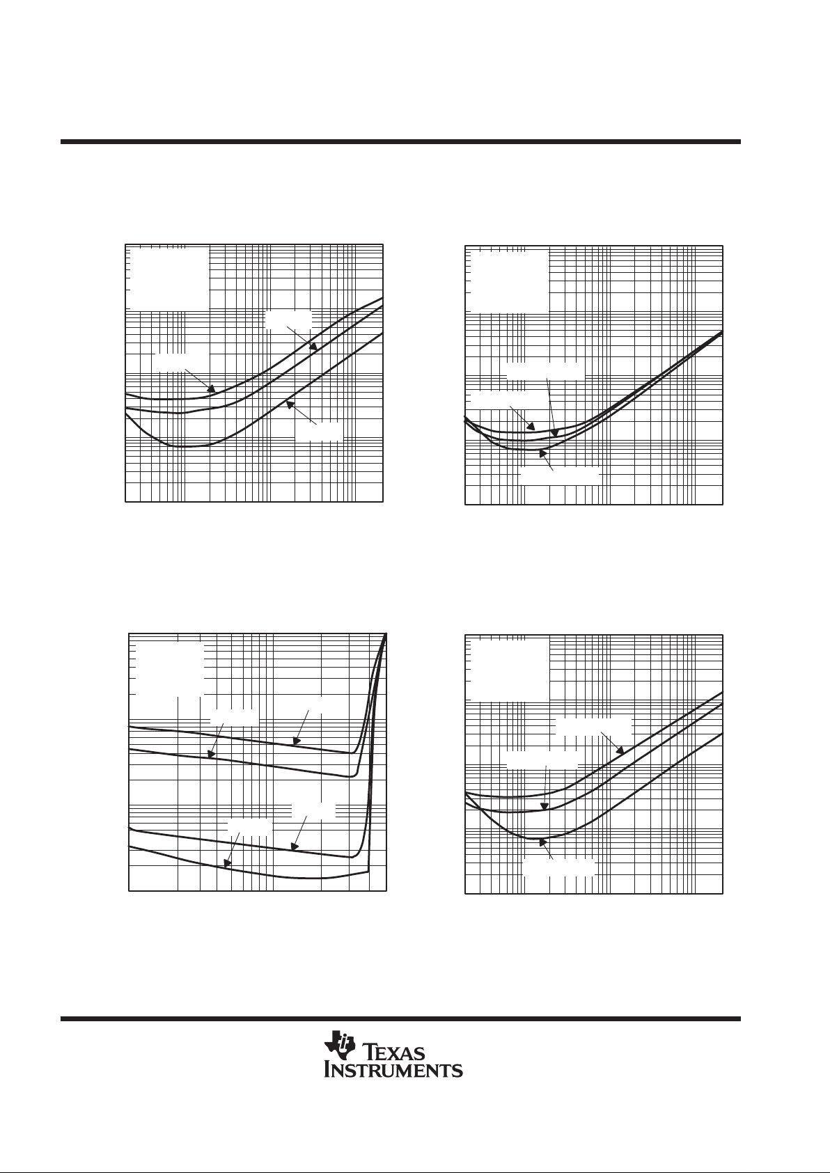
Page 7
TPA112
150-mW STEREO AUDIO POWER AMPLIFIER
SLOS212C – AUGUST 1998 – REVISED MARCH 2000
7
POST OFFICE BOX 655303 • DALLAS, TEXAS 75265
TYPICAL CHARACTERISTICS
Figure 5
0.1
0.01
0.001
1
10
20 100 1k 10k 20k
TOTAL HARMONIC DISTORTION PLUS NOISE
vs
FREQUENCY
VDD = 5 V
RL = 32 Ω
AV = 1 V/V
CB = 1 µF
PO = 15 mW
THD+N –Total Harmonic Distortion + Noise – %
f – Frequency – Hz
PO = 30 mW
PO = 60 mW
Figure 6
TOTAL HARMONIC DISTORTION PLUS NOISE
vs
OUTPUT POWER
THD+N –Total Harmonic Distortion + Noise – %
20 kHz
0.1
0.01
1
10
PO – Output Power – W
VDD = 5 V
AV = 1 V/V
RL = 32 Ω
CB = 1 µF
10 kHz
1 kHz
20 Hz
0.002 0.01 0.1 0.2
Figure 7
0.1
0.01
0.001
1
10
20 100 1k 10k 20k
TOTAL HARMONIC DISTORTION PLUS NOISE
vs
FREQUENCY
VDD = 3.3 V
RL = 10 kΩ
PO = 100 µF
CB = 1 µF
THD+N –Total Harmonic Distortion + Noise – %
f – Frequency – Hz
AV = 5 mW
AV = 2 mW
Figure 8
0.1
0.01
0.001
1
10
20 100 1k 10k 20k
TOTAL HARMONIC DISTORTION PLUS NOISE
vs
FREQUENCY
VDD = 3.3 V
RL = 10 kΩ
AV = 1 V/V
CB = 1 µF
THD+N –Total Harmonic Distortion + Noise – %
f – Frequency – Hz
PO = 45 µW
PO = 130 µW
PO = 90 µW
Page 8
TPA112
150-mW STEREO AUDIO POWER AMPLIFIER
SLOS212C – AUGUST 1998 – REVISED MARCH 2000
8
POST OFFICE BOX 655303 • DALLAS, TEXAS 75265
TYPICAL CHARACTERISTICS
Figure 9
5 10 100 200
TOTAL HARMONIC DISTORTION PLUS NOISE
vs
OUTPUT POWER
THD+N –Total Harmonic Distortion + Noise – %
20 Hz
0.01
0.001
1
10
PO – Output Power – µW
10 kHz
1 kHz
20 Hz
0.1
VDD = 3.3 V
RL = 10 k Ω
AV = 1 V/V
CB = 1 µF
Figure 10
0.1
0.01
0.001
1
10
20 100 1k 10k 20k
TOTAL HARMONIC DISTORTION PLUS NOISE
vs
FREQUENCY
VDD = 5 V
RL = 10 kΩ
PO = 300 µW
CB = 1 µF
THD+N –Total Harmonic Distortion + Noise – %
f – Frequency – Hz
AV = 1
AV = 2
AV = 5
Figure 11
0.1
0.01
0.001
1
10
20 100 1k 10k 20k
TOTAL HARMONIC DISTORTION PLUS NOISE
vs
FREQUENCY
VDD = 5 V
RL = 10 kΩ
AV = 1 V/V
CB = 1 µF
THD+N –Total Harmonic Distortion + Noise – %
f – Frequency – Hz
PO = 300 µW
PO = 200 µW
PO = 100 µW
Figure 12
0.1
0.01
0.001
1
10
5 10 100 500
TOTAL HARMONIC DISTORTION PLUS NOISE
vs
OUTPUT POWER
VDD = 5 V
RL = 10 kΩ
AV = 1 V/V
CB = 1 µ F
THD+N –Total Harmonic Distortion + Noise – %
20 Hz
1 kHz
20 kHz
10 kHz
PO – Output Power – µW
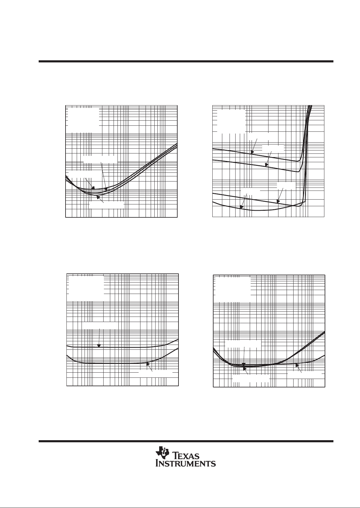
Page 9
TPA112
150-mW STEREO AUDIO POWER AMPLIFIER
SLOS212C – AUGUST 1998 – REVISED MARCH 2000
9
POST OFFICE BOX 655303 • DALLAS, TEXAS 75265
TYPICAL CHARACTERISTICS
Figure 13
20
TOTAL HARMONIC DISTORTION PLUS NOISE
vs
FREQUENCY
THD+N – Total Harmonic Distortion Plus Noise – %
f – Frequency – Hz
2
0.1
0.01
0.001
100 1k 10k 20k
1
AV = 1
AV = 2
AV = 5
VDD = 3.3 V
PO = 75 mW
RL = 8 Ω
CB = 1 µF
Figure 14
0.1
0.01
0.001
1
10
20 100 1k 10k 20k
TOTAL HARMONIC DISTORTION PLUS NOISE
vs
FREQUENCY
VDD = 3.3 V
RL = 8 Ω
AV = 1 V/V
THD+N –Total Harmonic Distortion + Noise – %
f – Frequency – Hz
PO = 75 mW
PO = 15 mW
PO = 30 mW
Figure 15
TOTAL HARMONIC DISTORTION PLUS NOISE
vs
OUTPUT POWER
20 kHz
0.1
0.01
1
10
THD+N –Total Harmonic Distortion + Noise – %
PO – Output Power – W
10m 0.1 0.3
VDD = 3.3 V
RL = 8 Ω
AV = 1 V/V
10 kHz
1 kHz
20 Hz
Figure 16
20
TOTAL HARMONIC DISTORTION PLUS NOISE
vs
FREQUENCY
THD+N – Total Harmonic Distortion Plus Noise – %
f – Frequency – Hz
2
0.1
0.01
0.001
100 1k 10k 20k
1
AV = 1
AV = 2
AV = 5
VDD = 5 V
PO = 100 mW
RL = 8 Ω
CB = 1 µF
Page 10
TPA112
150-mW STEREO AUDIO POWER AMPLIFIER
SLOS212C – AUGUST 1998 – REVISED MARCH 2000
10
POST OFFICE BOX 655303 • DALLAS, TEXAS 75265
TYPICAL CHARACTERISTICS
Figure 17
0.1
0.01
0.001
1
10
20 100 1k 10k 20k
TOTAL HARMONIC DISTORTION PLUS NOISE
vs
FREQUENCY
THD+N –Total Harmonic Distortion + Noise – %
f – Frequency – Hz
VDD = 5 V
RL = 8 kΩ
AV = 1 V/V
PO = 30 mW
PO = 60 mW
PO = 10 mW
Figure 18
TOTAL HARMONIC DISTORTION PLUS NOISE
vs
POWER OUTPUT
20 kHz
0.1
0.01
1
10
THD+N –Total Harmonic Distortion + Noise – %
PO – Output Power – W
10m 0.1 1
1 kHz
20 Hz
10 kHz
VDD = 5 V
RL = 8 Ω
AV = 1 V/V
Figure 19
POWER SUPPLY REJECTION RATIO
vs
FREQUENCY
20 100 20k
f – Frequency – Hz
1k
–50
–70
–90
–60
–80
–100
VDD = 3.3 V
RL = 8 Ω to 10 kΩ
–40
–10
–30
0
–20
PSRR – Power Supply Rejection Ratio – dB
10k
CB = 0.1 µF
CB = 1 µF
CB = 2 µF
Bypass = 1.65 V
Figure 20
POWER SUPPLY REJECTION RATIO
vs
FREQUENCY
20 100 20k
f – Frequency – Hz
1k
–50
–70
–90
–60
–80
–100
VDD = 5 V
RL = 8 Ω to 10 kΩ
–40
–10
–30
0
–20
PSRR – Power Supply Rejection Ratio – dB
10k
CB = 0.1 µF
CB = 1 µF
CB = 2 µF
Bypass = 2.5 V
Page 11
TPA112
150-mW STEREO AUDIO POWER AMPLIFIER
SLOS212C – AUGUST 1998 – REVISED MARCH 2000
11
POST OFFICE BOX 655303 • DALLAS, TEXAS 75265
TYPICAL CHARACTERISTICS
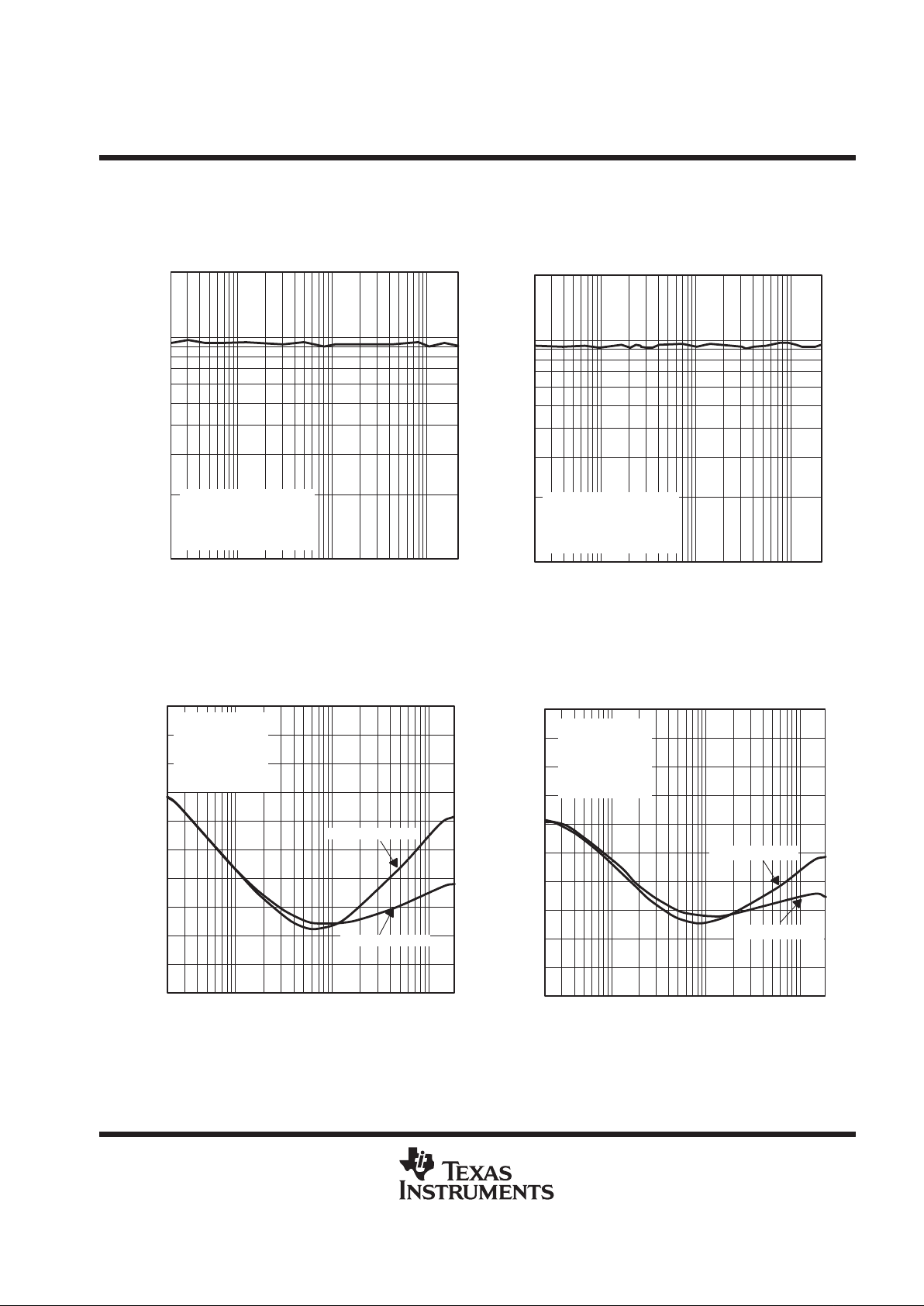
Figure 21
OUTPUT NOISE VOLTAGE
vs
FREQUENCY
20
f – Frequency – Hz
20 100 1k 10k 20k
VDD = 3.3 V
BW = 10 Hz to 22 kHz
AV = 1 V/V
RL = 8 Ω to 10 kΩ
– Output Noise Voltage – VµV
n
10
1
Figure 22
OUTPUT NOISE VOLTAGE
vs
FREQUENCY
1
10
20
f – Frequency – Hz
20 100 1k 10k 20k
VDD = 5 V
BW = 10 Hz to 22 kHz
RL = 8 Ω to 10 kΩ
AV = 1 V/V
– Output Noise Voltage – VµV
n
Figure 23
CROSSTALK
vs
FREQUENCY
20 100 20k
f – Frequency – Hz
1k
–85
–95
–105
–90
–100
–110
PO = 25 mW
VDD = 3.3 V
RL = 32 Ω
CB = 1 µF
AV = 1 V/V
–80
–65
–75
–60
–70
Crosstalk – dB
10k
IN 2 TO OUT 1
IN 1 TO OUT 2
Figure 24
CROSSTALK
vs
FREQUENCY
20 100 20k
f – Frequency – Hz
1k
–75
–85
–95
–80
–90
–100
PO = 100 mW
VDD = 3.3 V
RL = 8 Ω
CB = 1 µF
AV = 1 V/V
–70
–55
–65
–50
–60
Crosstalk – dB
10k
IN 2 TO OUT 1
IN 1 TO OUT 2
Page 12
TPA112
150-mW STEREO AUDIO POWER AMPLIFIER
SLOS212C – AUGUST 1998 – REVISED MARCH 2000
12
POST OFFICE BOX 655303 • DALLAS, TEXAS 75265
TYPICAL CHARACTERISTICS
Figure 25
CROSSTALK
vs
FREQUENCY
20 100 10k
f – Frequency – Hz
1k
–90
–100
–110
–95
–105
–85
–65
–80
–60
–75
–65
20k
VDD = 5 V
PO = 25 mW
CB = 1 µF
RL = 32 Ω
AV = 1 V/V
Crosstalk – dB
IN 2 TO OUT 1
IN 1 TO OUT 2
Figure 26
CROSSTALK
vs
FREQUENCY
20 100 10k
f – Frequency – Hz
1k
–80
–90
–100
–85
–95
–75
–55
–70
–50
–65
–60
20k
VDD = 5 V
PO = 100 mW
CB = 1 µF
RL = 8 Ω
AV = 1 V/V
Crosstalk – dB
IN 2 TO OUT 1
IN 1 TO OUT 2
Figure 27
MUTE ATTENUATION
vs
FREQUENCY
20 100 20k
f – Frequency – Hz
1k
–50
–70
–90
–60
–80
–100
VDD = 3.3 V
RL = 32 Ω
CB = 1 µF
–40
–10
–30
0
–20
Mute Attenuation – dB
10k
Figure 28
MUTE ATTENUATION
vs
FREQUENCY
20 100 10k
f – Frequency – Hz
1k
–60
–80
–100
–70
–90
–50
–10
–40
0
–30
–20
20k
VDD = 5 V
CB = 1 µF
RL = 32 Ω
Mute Attenuation – dB
Page 13
TPA112
150-mW STEREO AUDIO POWER AMPLIFIER
SLOS212C – AUGUST 1998 – REVISED MARCH 2000
13
POST OFFICE BOX 655303 • DALLAS, TEXAS 75265
TYPICAL CHARACTERISTICS
OPEN–LOOP GAIN AND PHASE MARGIN
vs
FREQUENCY
40
20
0
–20
60
80
–30°
0°
VDD = 3.3 V
TA = 25°C
No Load
100
30°
60°
90°
120°
150°
m
φ – Phase Margin
1k 100k
f – Frequency – Hz
10k 1M 10M100
Open-Loop Gain – dB
Phase
Gain
Figure 29
OPEN–LOOP GAIN AND PHASE MARGIN
vs
FREQUENCY
f – Frequency – Hz
20
0
–20
40
80
100 1k 10k 10M1M100k
60
Open-Loop Gain – dB
100
VDD = 5 V
TA = 25°C
No Load
–30°
0°
30°
60°
90°
120°
150°
Phase
Gain
m
φ – Phase Margin
Figure 30
Page 14

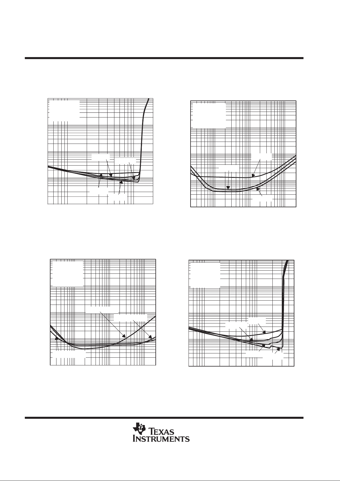
TPA112
150-mW STEREO AUDIO POWER AMPLIFIER
SLOS212C – AUGUST 1998 – REVISED MARCH 2000
14
POST OFFICE BOX 655303 • DALLAS, TEXAS 75265
TYPICAL CHARACTERISTICS
Figure 31
RL – Load Resistance – Ω
OUTPUT POWER
vs
LOAD RESISTANCE
100
40
0
16 32
80
60
20
24 40 64
120
8
48 56
THD+N = 1 %
VDD = 3.3 V
AV = 1 V/V
P
O
– Output Power – mW
Figure 32
OUTPUT POWER
vs
LOAD RESISTANCE
250
100
0
16 32
200
150
50
24 40 64
300
8
48 56
THD+N = 1 %
VDD = 5 V
AV = 1 V/V
P
O
– Output Power – mW
RL – Load Resistance – Ω
Figure 33
VDD – Supply Voltage – V
SUPPLY CURRENT
vs
SUPPLY VOLTAGE
1
0.6
0.2
34
0.8
0.4
0
3.5 4.5
1.4
2.5
5 5.5
1.2
I
DD
– Supply Current – mA
Figure 34
20
TOTAL HARMONIC DISTORTION PLUS NOISE
vs
FREQUENCY
THD+N – Total Harmonic Distortion Plus Noise – %
f – Frequency – Hz
1
0.1
0.01
0.001
100 1k 10k 20k
VI = 1 V
AV = 1 V/V
RL = 10 kΩ
CB = 1 µF
Page 15
TPA112
150-mW STEREO AUDIO POWER AMPLIFIER
SLOS212C – AUGUST 1998 – REVISED MARCH 2000
15
POST OFFICE BOX 655303 • DALLAS, TEXAS 75265
TYPICAL CHARACTERISTICS
Figure 35
1
SIGNAL–TO–NOISE RATIO
vs
VOLTAGE GAIN
SNR – Signal–to–Ratio – dB
AV – Voltage Gain – V/V
104
100
96
92
57910
94
98
102
86243
VI = 1 V
Figure 36
20
TOTAL HARMONIC DISTORTION PLUS NOISE
vs
FREQUENCY
THD+N – Total Harmonic Distortion Plus Noise – %
f – Frequency – Hz
1
0.1
0.01
0.001
100 1k 10k 20k
VDD = 5 V
AV = 1
RL = 10 kΩ
CB = 1 µF
Figure 37
20
CROSSTALK
vs
FREQUENCY
Crosstalk – dB
f – Frequency – Hz
–60
–100
–150
100 1k 10k 20k
–70
–80
–90
–110
–120
–130
–140
VDD = 3.3 V
VO = 1 V
RL = 10 kΩ
CB = 1 µF
IN2 to OUT1
IN1 to OUT2
Figure 38
20
CROSSTALK
vs
FREQUENCY
Crosstalk – dB
f – Frequency – Hz
–60
–100
–150
100 1k 10k 20k
–70
–80
–90
–110
–120
–130
–140
VDD = 5 V
VO = 1 V
RL = 10 kΩ
CB = 1 µF
IN1 to OUT2
IN2 to OUT1
Page 16

TPA112
150-mW STEREO AUDIO POWER AMPLIFIER
SLOS212C – AUGUST 1998 – REVISED MARCH 2000
16
POST OFFICE BOX 655303 • DALLAS, TEXAS 75265
TYPICAL CHARACTERISTICS
10
CLOSED–LOOP GAIN AND PHASE
vs
FREQUENCY
Closed–Loop Gain – dB
f – Frequency – Hz
–10
100 1k 10k 1M
30
20
10
0
100k
200°
180°
160°
140°
120°
100°
80°
Gain
Phase
Phase
VDD = 3.3 V
RI = 20 kΩ
RF = 20 kΩ
RL = 32 Ω
CI = 1 µF
AV = –1 V/V
Figure 39
10
CLOSED–LOOP GAIN AND PHASE
vs
FREQUENCY
Closed–Loop Gain – dB
f – Frequency – Hz
–10
100 1k 10k 1M
30
20
10
0
100k
Phase
200°
180°
160°
140°
120°
100°
80°
Gain
Phase
VDD = 5 V
RI = 20 kΩ
RF = 20 kΩ
RL = 32 Ω
CI = 1 µF
AV = –1 V/V
Figure 40
Page 17

TPA112
150-mW STEREO AUDIO POWER AMPLIFIER
SLOS212C – AUGUST 1998 – REVISED MARCH 2000
17
POST OFFICE BOX 655303 • DALLAS, TEXAS 75265
TYPICAL CHARACTERISTICS
10
CLOSED–LOOP GAIN AND PHASE
vs
FREQUENCY
Closed–Loop Gain – dB
f – Frequency – Hz
–20
100 1k 10k 1M
40
20
0
100k
Phase
200°
180°
160°
140°
120°
100°
80°
60°
Gain
Phase
VDD = 3.3 V
RI = 20 kΩ
RF = 20 kΩ
RL = 8 Ω
CI = 1 µF
AV = –1 V/V
Figure 41
10
CLOSED–LOOP GAIN AND PHASE
vs
FREQUENCY
Closed–Loop Gain – dB
f – Frequency – Hz
–10
100 1k 10k 1M
30
20
10
0
100k
Phase
200°
180°
160°
140°
120°
100°
80°
Gain
Phase
VDD = 3.3 V
RI = 20 kΩ
RF = 20 kΩ
RL = 10 kΩ
CI = 1 µF
AV = –1 V/V
Figure 42
Page 18

TPA112
150-mW STEREO AUDIO POWER AMPLIFIER
SLOS212C – AUGUST 1998 – REVISED MARCH 2000
18
POST OFFICE BOX 655303 • DALLAS, TEXAS 75265
TYPICAL CHARACTERISTICS
10
CLOSED–LOOP GAIN AND PHASE
vs
FREQUENCY
Closed–Loop Gain – dB
f – Frequency – Hz
–20
100 1k 10k 1M
20
0
100k
Phase
200°
180°
160°
140°
120°
100°
80°
60°
40°
Gain
Phase
VDD = 5 V
RI = 20 kΩ
RF = 20 kΩ
RL = 8 Ω
CI = 1 µF
AV = –1 V/V
Figure 43
10
CLOSED–LOOP GAIN AND PHASE
vs
FREQUENCY
Closed–Loop Gain – dB
f – Frequency – Hz
–10
100 1k 10k 1M
30
20
10
0
100k
Phase
200°
180°
160°
140°
120°
100°
80°
Gain
Phase
VDD = 5 V
RI = 20 kΩ
RF = 20 kΩ
RL = 10 kΩ
CI = 1 µF
AV = –1 V/V
Figure 44
Page 19

TPA112
150-mW STEREO AUDIO POWER AMPLIFIER
SLOS212C – AUGUST 1998 – REVISED MARCH 2000
19
POST OFFICE BOX 655303 • DALLAS, TEXAS 75265
TYPICAL CHARACTERISTICS
Figure 45
0
POWER DISSIPATION/AMPLIFIER
vs
OUTPUT POWER
Amplifier Power – mW
Load Power – mW
80
40
20
0
80 120 180 200
10
30
50
14010020 6040
160
60
70
VDD = 3.3 V
8 Ω
16 Ω
64 Ω
32 Ω
Figure 46
0
POWER DISSIPATION/AMPLIFIER
vs
OUTPUT POWER
Amplifier Power – mW
Load Power – mW
180
100
60
0
80 120 180 200
40
80
120
14010020 6040
160
140
160
VDD = 5 V
8 Ω
16 Ω
64 Ω
32 Ω
20
APPLICATION INFORMATION
gain setting resistors, R
F
and R
I
The gain for the TPA112 is set by resistors RF and RI according to equation 1.
(1)
Gain
+*
ǒ
R
F
R
I
Ǔ
Given that the TPA112 is a MOS amplifier, the input impedance is very high. Consequently input leakage
currents are not generally a concern, although noise in the circuit increases as the value of RF increases. In
addition, a certain range of RF values is required for proper start-up operation of the amplifier. Taken together
it is recommended that the effective impedance seen by the inverting node of the amplifier be set between
5 kΩ and 20 kΩ. The effective impedance is calculated in equation 2.
(2)
Effective Impedance
+
R
FRI
RF)
R
I
As an example, consider an input resistance of 20 kΩ and a feedback resistor of 20 kΩ. The gain of the amplifier
would be – 1 and the effective impedance at the inverting terminal would be 10 kΩ, which is within the
recommended range.
Page 20

TPA112
150-mW STEREO AUDIO POWER AMPLIFIER
SLOS212C – AUGUST 1998 – REVISED MARCH 2000
20
POST OFFICE BOX 655303 • DALLAS, TEXAS 75265
APPLICATION INFORMATION
Page 21

TPA112
150-mW STEREO AUDIO POWER AMPLIFIER
SLOS212C – AUGUST 1998 – REVISED MARCH 2000
21
POST OFFICE BOX 655303 • DALLAS, TEXAS 75265
gain setting resistors, RF and RI (continued)
For high performance applications, metal film resistors are recommended because they tend to have lower
noise levels than carbon resistors. For values of RF above 50 kΩ, the amplifier tends to become unstable due
to a pole formed from RF and the inherent input capacitance of the MOS input structure. For this reason, a small
compensation capacitor of approximately 5 pF should be placed in parallel with R
F
. This, in effect, creates a
low-pass filter network with the cutoff frequency defined in equation 3.
(3)
f
co(lowpass)
+
1
2pRFC
F
For example, if RF is 100 kΩ and CF is 5 pF then f
co(lowpass)
is 318 kHz, which is well outside the audio range.
input capacitor, C
I
In the typical application, an input capacitor, CI, is required to allow the amplifier to bias the input signal to the
proper dc level for optimum operation. In this case, C
I
and RI form a high-pass filter with the corner frequency
determined in equation 4.
(4)
f
co(highpass)
+
1
2pRIC
I
The value of CI is important to consider, as it directly af fects the bass (low frequency) performance of the circuit.
Consider the example where R
I
is 20 kΩ and the specification calls for a flat bass response down to 20 Hz.
Equation 4 is reconfigured as equation 5.
(5)
CI+
1
2pR
I
f
co(highpass)
In this example, CI is 0.40 µF, so one would likely choose a value in the range of 0.47 µF to 1 µF. A further
consideration for this capacitor is the leakage path from the input source through the input network (RI, CI) and
the feedback resistor (RF) to the load. This leakage current creates a dc offset voltage at the input to the amplifier
that reduces useful headroom, especially in high-gain applications (> 10). For this reason a low-leakage
tantalum or ceramic capacitor is the best choice. When polarized capacitors are used, the positive side of the
capacitor should face the amplifier input in most applications, as the dc level there is held at V
DD
/2, which is
likely higher that the source dc level. It is important to confirm the capacitor polarity in the application.
power supply decoupling, C
S
The TP A112 is a high-performance CMOS audio amplifier that requires adequate power supply decoupling to
ensure that the output total harmonic distortion (THD) is as low as possible. Power supply decoupling also
prevents oscillations for long lead lengths between the amplifier and the speaker. The optimum decoupling is
achieved by using two capacitors of different types that target different types of noise on the power supply leads.
For higher frequency transients, spikes, or digital hash on the line, a good low equivalent-series-resistance
(ESR) ceramic capacitor, typically 0.1 µF, placed as close as possible to the device V
DD
lead, works best. For
filtering lower-frequency noise signals, a larger aluminum electrolytic capacitor of 10 µF or greater placed near
the power amplifier is recommended.
Page 22

TPA112
150-mW STEREO AUDIO POWER AMPLIFIER
SLOS212C – AUGUST 1998 – REVISED MARCH 2000
22
POST OFFICE BOX 655303 • DALLAS, TEXAS 75265
APPLICATION INFORMATION
midrail voltage
The TP A112 is a single-supply amplifier , so it must be properly biased to accommodate audio signals. Normally ,
the amplifier is biased at VDD/2, but it can actually be biased at any voltage between VDD and ground. However,
biasing the amplifier at a point other than VDD/2 will reduce the amplifier’s maximum output swing. In some
applications where the circuitry driving the TP A112 has a different midrail voltage, it might make sense to use
the same midrail voltage for the TPA112, and possibly eliminate the use of the dc-blocking caps.
There are two concerns with the midrail voltage source: the amount of noise present, and its output impedance.
Any noise present on the midrail voltage source that is not present on the audio input signal will be input to the
amplifier, and passed to the output (and increased by the gain of the circuit). Common-mode noise will be
cancelled out by the differential configuration of the circuit.
The output impedance of the circuit used to generate the midrail voltage needs to be low enough so as not to
be influenced by the audio signal path. A common method of generating the midrail voltage is to form a voltage
divider from the supply to ground, with a bypass capacitor from the common node to ground. This capacitor
improves the PSRR of the circuit. However, this circuit has a limited range of output impedances, so to achieve
very low output impedances, the voltage generated by the voltage divider is fed into a unity-gain amplifier to
lower the output impedance of the circuit.
_
+
V
DD
R
R
Midrail
C
BYPASS
V
DD
R
R
Midrail
C
BYPASS
TLV2460
a) Midrail Voltage Generator Using a Simple
Resistor-Divider
b) Buffered Midrail Voltage Generator to Provide
Low Output Impedance
Figure 47. Midrail Voltage Generator
If a voltage step is applied to a speaker, it will pop. To reduce popping, the midrail voltage should rise at a
sub-sonic rate; that is, a rate less than the rise time of a 20-Hz waveform. If the voltage rises faster than that,
there is the possibility of a pop from the speaker.
Pop can also be heard in the speaker if the midrail voltage rises faster than either the input coupling capacitor,
or the output coupling capacitor. If midrail rises first, then the charging of the input and output capacitors will
be heard in the speaker. To keep this noise as low as possible, the relationship shown in equation 6 should be
maintained.
(6)
1
ǒ
CB
R
SOURCE
Ǔ
v
1
ǒ
CIR
I
Ǔ
Ơ
1
RLC
C
Where C
BYPASS
is the value of the bypass capacitor, and R
SOURCE
is the equivalent source impedance of the
voltage divider (the parallel combination of the two resistors). For example, if the voltage divider is constructed
using two 20-kΩ resistors, then R
SOURCE
is 10 kΩ.
Page 23

TPA112
150-mW STEREO AUDIO POWER AMPLIFIER
SLOS212C – AUGUST 1998 – REVISED MARCH 2000
23
POST OFFICE BOX 655303 • DALLAS, TEXAS 75265
APPLICATION INFORMATION
midrail bypass capacitor, C
B
The midrail bypass capacitor, CB, serves several important functions. During start-up, CB determines the rate
at which the amplifier starts up. This helps to push the start-up pop noise into the subaudible range (so slow
it can not be heard). The second function is to reduce noise produced by the power supply caused by coupling
into the output drive signal. This noise is from the midrail generation circuit internal to the amplifier. The capacitor
is fed from the resistor divider with equivalent resistance of R
SOURCE
. To keep the start-up pop as low as
possible, the relationship shown in equation 7 should be maintained.
(7)
1
ǒ
CB
R
SOURCE
Ǔ
v
1
ǒ
CIR
I
Ǔ
As an example, consider a circuit where CB is 1 µF, R
SOURCE
= 160 kΩ, CI is 1 µF, and RI is 20 kΩ. Inserting
these values into the equation 9 results in:
6.25v50
which satisfies the rule. Bypass capacitor, CB, values of 0.1 µF to 1 µF ceramic or tantalum low-ESR capacitors
are recommended for the best THD and noise performance.
output coupling capacitor, C
C
In the typical single-supply single-ended (SE) configuration, an output coupling capacitor (CC) is required to
block the dc bias at the output of the amplifier, thus preventing dc currents in the load. As with the input coupling
capacitor, the output coupling capacitor and impedance of the load form a high-pass filter governed by
equation 8.
(8)
f
(out high)
+
1
2pRLC
C
The main disadvantage, from a performance standpoint, is that the typically small load impedances drive the
low-frequency corner higher. Large values of CC are required to pass low frequencies into the load. Consider
the example where a CC of 68 µF is chosen and loads vary from 32 Ω to 47 kΩ. Table 1 summarizes the
frequency response characteristics of each configuration.
Table 1. Common Load Impedances vs Low Frequency Output Characteristics in SE Mode
R
L
C
C
Lowest Frequency
32 Ω 68 µF
73 Hz
10,000 Ω 68 µF 0.23 Hz
47,000 Ω 68 µF 0.05 Hz
As Table 1 indicates, headphone response is adequate and drive into line level inputs (a home stereo for
example) is very good.
Page 24

TPA112
150-mW STEREO AUDIO POWER AMPLIFIER
SLOS212C – AUGUST 1998 – REVISED MARCH 2000
24
POST OFFICE BOX 655303 • DALLAS, TEXAS 75265
APPLICATION INFORMATION
Page 25

TPA112
150-mW STEREO AUDIO POWER AMPLIFIER
SLOS212C – AUGUST 1998 – REVISED MARCH 2000
25
POST OFFICE BOX 655303 • DALLAS, TEXAS 75265
output coupling capacitor, CC (continued)
The output coupling capacitor required in single-supply SE mode also places additional constraints on the
selection of other components in the amplifier circuit. With the rules described earlier still valid, add the following
relationship:
output pull-down resistor, RC + R
O
Placing a 100-Ω resistor, RC, from the output side of the coupling capacitor to ground insures the coupling
capacitor, CC, is charged before a plug is inserted into the jack. Without this resistor, the coupling capacitor
would charge rapidly upon insertion of a plug, leading to an audible pop in the headphones.
Placing a 20-kΩ resistor, RO, from the output of the IC to ground insures that the coupling capacitor fully
discharges at power down. If the supply is rapidly cycled without this capacitor, a small pop may be audible in
10-kΩ loads.
using low-ESR capacitors
Low-ESR capacitors are recommended throughout this application. A real capacitor can be modeled simply
as a resistor in series with an ideal capacitor. The voltage drop across this resistor minimizes the beneficial
effects of the capacitor in the circuit. The lower the equivalent value of this resistance, the more the real
capacitor behaves like an ideal capacitor.
5-V versus 3.3-V operation
The TPA112 was designed for operation over a supply range of 2.7 V to 5.5 V. This data sheet provides full
specifications for 5-V and 3.3-V operation since these are considered to be the two most common standard
voltages. There are no special considerations for 3.3-V versus 5-V operation as far as supply bypassing, gain
setting, or stability. Supply current is slightly reduced from 3.5 mA (typical) to 2.5 mA (typical). The most
important consideration is that of output power. Each amplifier in the TPA112 can produce a maximum voltage
swing of V
DD
– 1 V . This means, for 3.3-V operation, clipping starts to occur when V
O(PP)
= 2.3 V as opposed
when V
O(PP)
= 4 V while operating at 5 V . The reduced voltage swing subsequently reduces maximum output
power into the load before distortion begins to become significant.
Page 26
TPA112
150-mW STEREO AUDIO POWER AMPLIFIER
SLOS212C – AUGUST 1998 – REVISED MARCH 2000
26
POST OFFICE BOX 655303 • DALLAS, TEXAS 75265
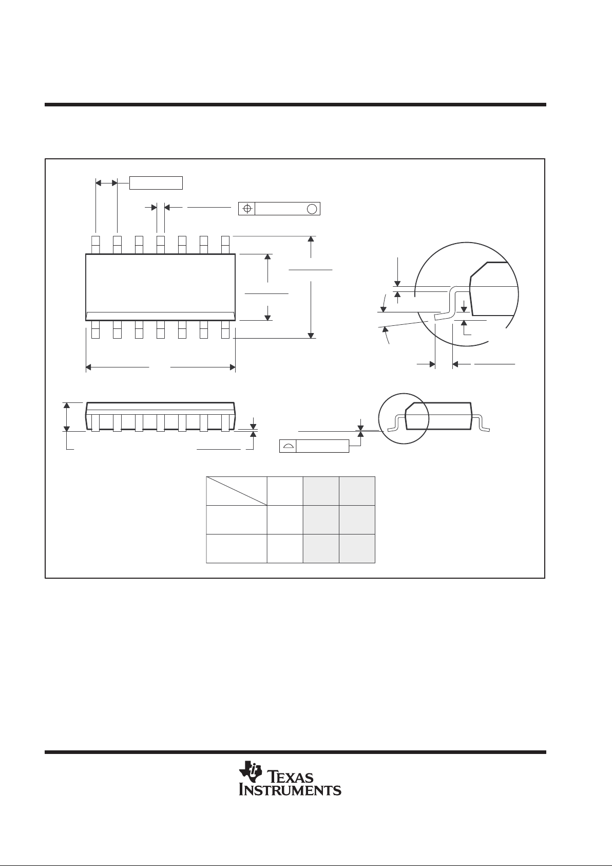
MECHANICAL DATA
D (R-PDSO-G**) PLASTIC SMALL-OUTLINE PACKAGE
14 PINS SHOWN
4040047/D 10/96
0.228 (5,80)
0.244 (6,20)
0.069 (1,75) MAX
0.010 (0,25)
0.004 (0,10)
1
14
0.014 (0,35)
0.020 (0,51)
A
0.157 (4,00)
0.150 (3,81)
7
8
0.044 (1,12)
0.016 (0,40)
Seating Plane
0.010 (0,25)
PINS **
0.008 (0,20) NOM
A MIN
A MAX
DIM
Gage Plane
0.189
(4,80)
(5,00)
0.197
8
(8,55)
(8,75)
0.337
14
0.344
(9,80)
16
0.394
(10,00)
0.386
0.004 (0,10)
M
0.010 (0,25)
0.050 (1,27)
0°–8°
NOTES: A. All linear dimensions are in inches (millimeters).
B. This drawing is subject to change without notice.
C. Body dimensions do not include mold flash or protrusion, not to exceed 0.006 (0,15).
D. Falls within JEDEC MS-012
Page 27
TPA112
150-mW STEREO AUDIO POWER AMPLIFIER
SLOS212C – AUGUST 1998 – REVISED MARCH 2000
27
POST OFFICE BOX 655303 • DALLAS, TEXAS 75265
MECHANICAL DATA
DGN (S-PDSO-G8) PowerPAD PLASTIC SMALL-OUTLINE PACKAGE
0,69
0,41
0,25
Thermal Pad
(See Note D)
0,15 NOM
Gage Plane
4073271/A 04/98
4,98
0,25
5
3,05
4,78
2,95
8
4
3,05
2,95
1
0,38
0,15
0,05
1,07 MAX
Seating Plane
0,10
0,65
M
0,25
0°–6°
NOTES: A. All linear dimensions are in millimeters.
B. This drawing is subject to change without notice.
C. Body dimensions include mold flash or protrusions.
D. The package thermal performance may be enhanced by attaching an external heat sink to the thermal pad.
This pad is electrically and thermally connected to the backside of the die and possibly selected leads.
E. Falls within JEDEC MO-187
PowerPAD is a trademark of Texas Instruments.
Page 28

IMPORTANT NOTICE
T exas Instruments and its subsidiaries (TI) reserve the right to make changes to their products or to discontinue
any product or service without notice, and advise customers to obtain the latest version of relevant information
to verify, before placing orders, that information being relied on is current and complete. All products are sold
subject to the terms and conditions of sale supplied at the time of order acknowledgment, including those
pertaining to warranty, patent infringement, and limitation of liability.
TI warrants performance of its semiconductor products to the specifications applicable at the time of sale in
accordance with TI’s standard warranty. Testing and other quality control techniques are utilized to the extent
TI deems necessary to support this warranty. Specific testing of all parameters of each device is not necessarily
performed, except those mandated by government requirements.
Customers are responsible for their applications using TI components.
In order to minimize risks associated with the customer’s applications, adequate design and operating
safeguards must be provided by the customer to minimize inherent or procedural hazards.
TI assumes no liability for applications assistance or customer product design. TI does not warrant or represent
that any license, either express or implied, is granted under any patent right, copyright, mask work right, or other
intellectual property right of TI covering or relating to any combination, machine, or process in which such
semiconductor products or services might be or are used. TI’s publication of information regarding any third
party’s products or services does not constitute TI’s approval, warranty or endorsement thereof.
Copyright 2000, Texas Instruments Incorporated
 Loading...