

TPA0213
2-W MONO AUDIO POWER AMPLIFIER
WITH HEADPHONE DRIVE
SLOS276B – JANUARY 2000 – REVISED MARCH 2000
DD
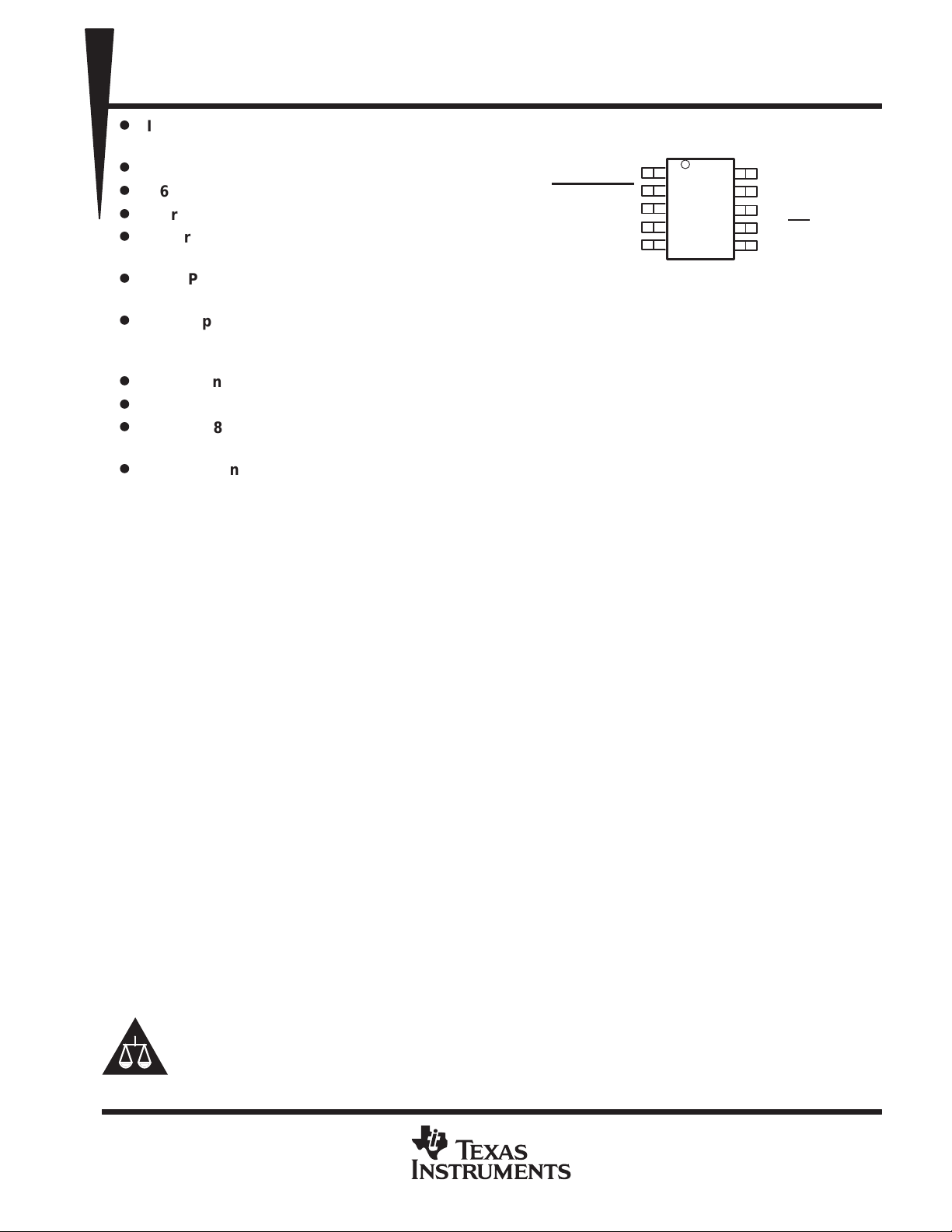
DGQ PACKAGE
(TOP VIEW)
1
2
3
4
5
10
9
8
7
6
LO/MO–
LIN
GND
ST/MN
RO/MO+
D
Ideal for Notebook Computers, PDAs, and
Other Small Portable Audio Devices
D
2 W Into 4-Ω From 5-V Supply
D
0.6 W Into 4-Ω From 3-V Supply
D
Stereo Head Phone Drive
D
Separate Inputs for the Mono (BTL) Signal,
and Stereo (SE) Left/Right Signals
D
Wide Power Supply Compatibility 2.5 V to
MONO–IN
SHUTDOWN
V
BYPASS
RIN
5.5 V
D
Low Supply Current
– 4.2 mA Typical at 5 V
– 3.6 mA Typical at 3 V
D
Shutdown Control ...1 µA Typical
D
Shutdown Pin is TTL Compatible
D
–40°C to 85°C Operating Temperature
Range
D
Space-Saving, Thermally-Enhanced MSOP
Packaging
description
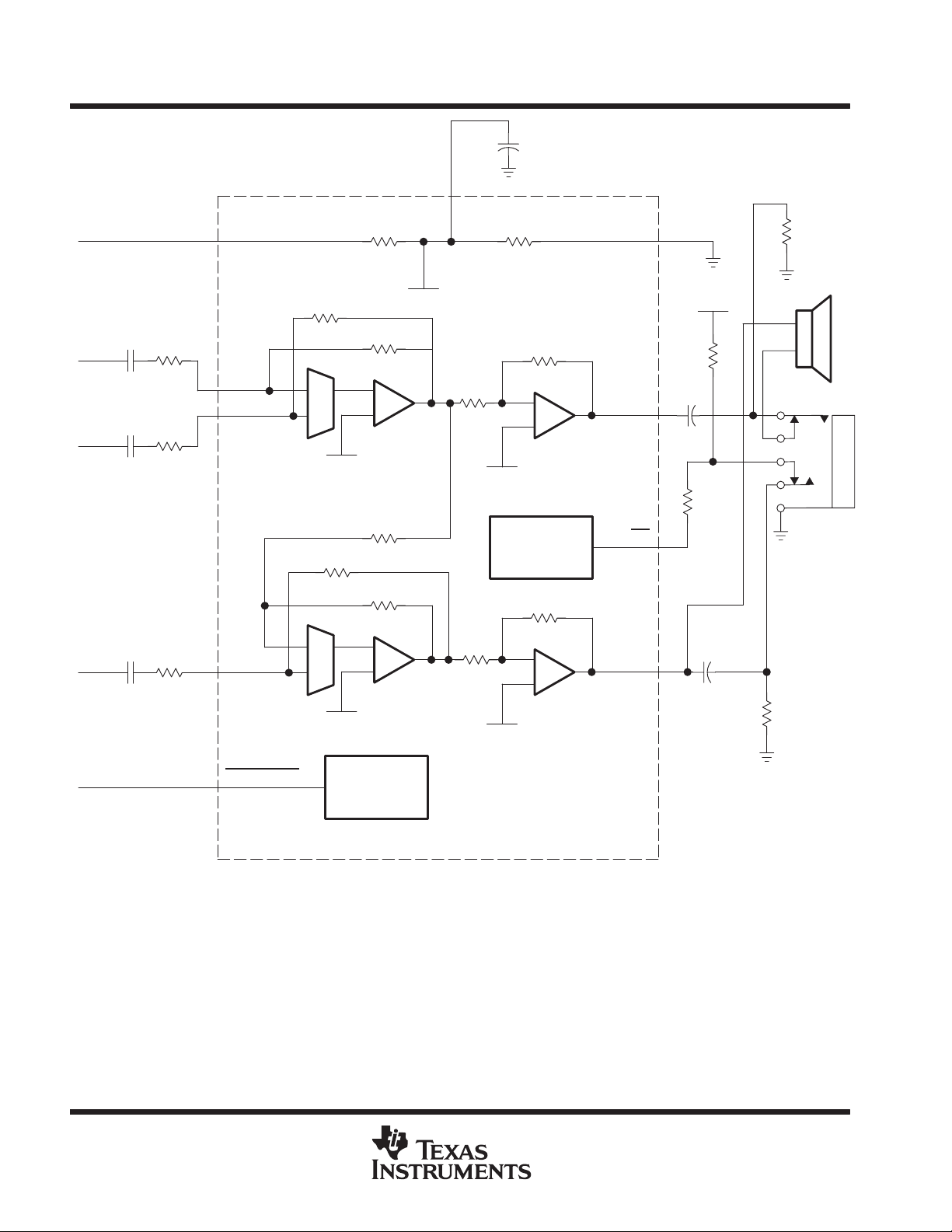
The TPA0213 is a 2-W mono bridge-tied-load (BTL) amplifier designed to drive speakers with as low as 4-Ω
impedance. The amplifier can be reconfigured on-the-fly to drive two stereo single-ended (SE) signals into head
phones. This makes the device ideal for use in small notebook computers, PDAs, Digital Personal Audio
players, anyplace a mono speaker and stereo head phones are required. From a 5-V supply , the TP A0213 can
deliver 2-W of power into a 4-Ω speaker.
The gain of the input stage is set by the user-selected input resistor and a 50-kΩ internal feedback resistor
(AV = – RF/ RI). The power stage is internally configured with a gain of –1.25 V/V in SE mode, and –2.5 V/V in
BTL mode. Thus, the overall gain of the amplifier is 62.5 kΩ/ R
in SE mode and 125 kΩ/ RI in BTL mode.
I
The TPA0213 is available in the 10-pin thermally-enhanced MSOP package (DGQ) and operates over an
ambient temperature range of –40°C to 85°C.
Please be aware that an important notice concerning availability, standard warranty, and use in critical applications of
Texas Instruments semiconductor products and disclaimers thereto appears at the end of this data sheet.
PowerPAD is a trademark of Texas Instruments Incorporated.
PRODUCTION DATA information is current as of publication date.
Products conform to specifications per the terms of Texas Instruments
standard warranty. Production processing does not necessarily include
testing of all parameters.
Copyright 2000, Texas Instruments Incorporated
POST OFFICE BOX 655303 • DALLAS, TEXAS 75265
1
TPA0213
2-W MONO AUDIO POWER AMPLIFIER
WITH HEADPHONE DRIVE
SLOS276B – JANUARY 2000 – REVISED MARCH 2000
V
DD
V
DD
3
4
BYPASS
C
B
GND
8
1 kΩ
Mono
Audio
Input
Right
Audio
Input
Left
Audio
Input
From
System Control
C
I
C
I
C
I
100 kΩ
C
6
7
10
V
DD
C
100 kΩ
C
C
1 kΩ
50 kΩ
–
+
50 kΩ
50 kΩ
–
+
BYPASS
R
BYPASS
R
BYPASS
1.25*R
–
+
Stereo/Mono
Control
1.25*R
–
+
RO/MO+
ST/MN
LO/MO–
50 kΩ
R
I
1
MONO-IN
5
R
I
R
I
RIN
9
LIN
2
SHUTDOWN
M
U
X
BYPASS
50 kΩ
M
U
X
BYPASS
Shutdown
and Depop
Circuitry
2
POST OFFICE BOX 655303 • DALLAS, TEXAS 75265
MSOP
I/O
DESCRIPTION
2-W MONO AUDIO POWER AMPLIFIER
WITH HEADPHONE DRIVE
SLOS276B – JANUARY 2000 – REVISED MARCH 2000
AVAILABLE OPTIONS
PACKAGED DEVICES
T
A
–40°C to 85°C TPA0213DGQ AEH
†
The DGQ package are available taped and reeled. To order a taped and reeled part, add the
suffix R to the part number (e.g., TPA0213DGQR).
Terminal Functions
TERMINAL
NAME NO.
MONO-IN 1 I Mono input terminal
SHUTDOWN 2 I SHUTDOWN places the entire device in shutdown mode when held low. TTL compatible input.
V
DD
BYPASS 4 I BYPASS is the tap to the voltage divider for internal mid-supply bias. This terminal should be connected
RIN 5 I Right-channel input terminal
RO/MO+ 6 O Right-output in SE mode and mono positive output in BTL mode
ST/MN 7 I Selects between stereo and mono mode. When held high, the amplifier is in SE stereo mode, while held
GND 8 Ground terminal
LIN 9 I Left-channel input terminal
LO/MO– 10 O Left-output in SE mode and mono negative output in BTL mode.
3 I VDD is the supply voltage terminal.
to a 0.1-µF to 1-µF capacitor.
low, the amplifier is in BTL mono mode.
MSOP
(DGQ)
†
SYMBOLIZATION
TPA0213
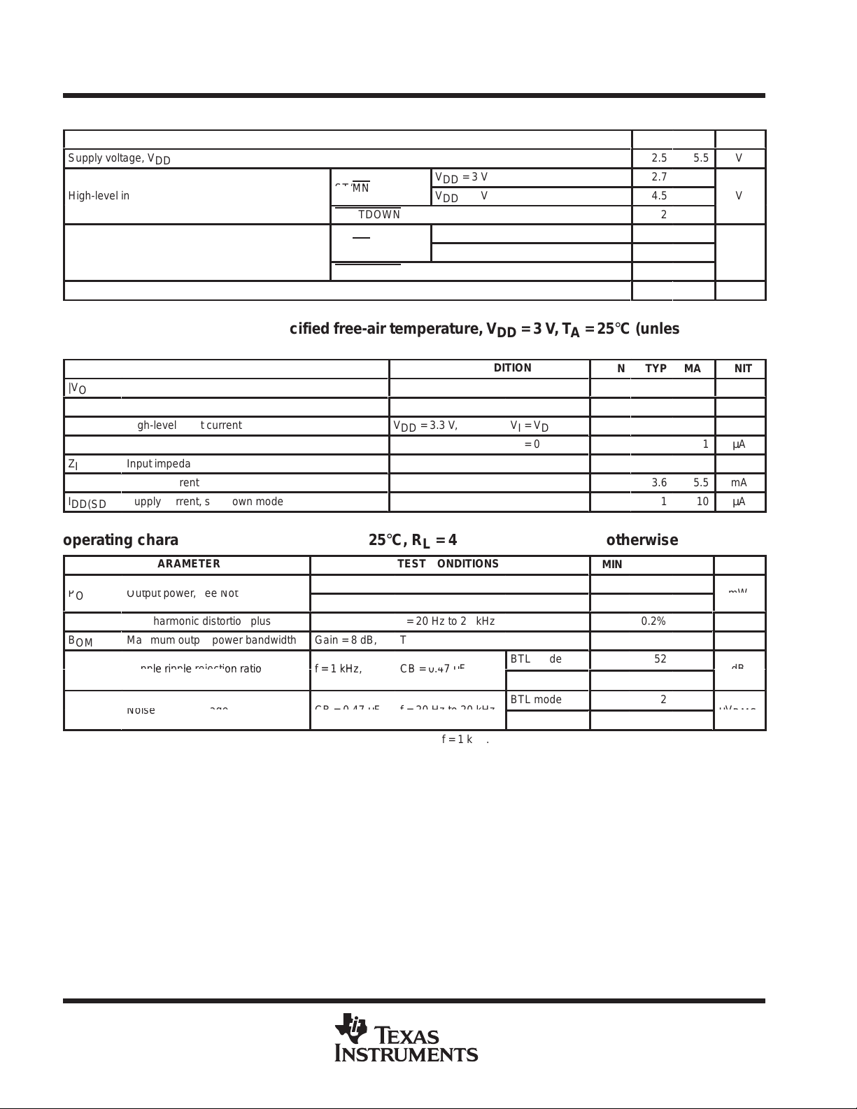
absolute maximum ratings over operating free-air temperature range (unless otherwise noted)
Supply voltage, V
Input voltage, V
Continuous total power dissipation internally limited (see Dissipation Rating Table). . . . . . . . . . . . . . . . . . . . .
Operating free-air temperature range, TA (see Table 3) –40°C to 85°C. . . . . . . . . . . . . . . . . . . . . . . . . . . . . . . .
Operating junction temperature range, TJ –40°C to 150°C. . . . . . . . . . . . . . . . . . . . . . . . . . . . . . . . . . . . . . . . . . .
Storage temperature range, T
Lead temperature 1,6 mm (1/16 inch) from case for 10 seconds 260°C. . . . . . . . . . . . . . . . . . . . . . . . . . . . . . .
§
Stresses beyond those listed under “absolute maximum ratings” may cause permanent damage to the device. These are stress ratings only, and
functional operation of the device at these or any other conditions beyond those indicated under “recommended operating conditions” is not
implied. Exposure to absolute-maximum-rated conditions for extended periods may affect device reliability.
PACKAGE
¶
Please see the Texas Instruments document,
(literature number SLMA002), for more information on the PowerPAD package. The thermal data was
measured on a PCB layout based on the information in the section entitled
Board for PowerPAD
6 V. . . . . . . . . . . . . . . . . . . . . . . . . . . . . . . . . . . . . . . . . . . . . . . . . . . . . . . . . . . . . . . . . . . . . . . .
DD
–0.3 V to VDD +0.3 V. . . . . . . . . . . . . . . . . . . . . . . . . . . . . . . . . . . . . . . . . . . . . . . . . . . . . . . . . . . .
I
–65°C to 150°C. . . . . . . . . . . . . . . . . . . . . . . . . . . . . . . . . . . . . . . . . . . . . . . . . . .
stg
DISSIPATION RATING TABLE
TA ≤ 25°C DERATING FACTOR TA = 70°C TA = 85°C
DGQ 2.14 W
on page 33 of the before mentioned document.
¶
17.1 mW/°C 1.37 W 1.11 W
PowerPAD Thermally Enhanced Package Application Report
T exas Instruments Recommended
§
POST OFFICE BOX 655303 • DALLAS, TEXAS 75265
3
TPA0213
ST/MN
ST/MN
POOutput power, see Note 1
mW
Su le ri le rejection ratio
f
kHz
CB
µF
dB
VnNoise output voltage
CB
V
2-W MONO AUDIO POWER AMPLIFIER
WITH HEADPHONE DRIVE
SLOS276B – JANUARY 2000 – REVISED MARCH 2000
recommended operating conditions
MIN MAX UNIT
Supply voltage, V
High-level input voltage, V
Low-level input voltage, V
Operating free-air temperature, T
DD
VDD = 3 V 2.7
IH
SHUTDOWN 2
IL
SHUTDOWN 0.8
A
VDD = 5 V 4.5
VDD = 3 V 1.65
VDD = 5 V 2.75
electrical characteristics at specified free-air temperature, VDD = 3 V , TA = 25°C (unless otherwise
noted)
PARAMETER TEST CONDITIONS
|VOO|
PSRR
|IIH| High-level input current VDD = 3.3 V, VI = V
|IIL| Low-level input current VDD = 3.3 V, VI = 0
Z
I
I
DD
I
DD(SD)
Output offset voltage (measured differentially)
Power supply rejection ratio
Input impedance
Supply current
Supply current, shutdown mode
VIO = 0, Gain = 8 dB
VDD = 2.9 V to 3.1 V,
BTL mode
DD
MIN TYP MAX UNIT
2.5
–40
65
50
3.6
5.5
5.5
1
85
30
10
V
V
V
°C
mV
dB
1
µA
1
µA
kΩ
mA
µA
operating characteristics, VDD = 3 V, T
PARAMETER TEST CONDITIONS
p
p
THD + N
B
OM
NOTE 1: Output power is measured at the output terminals of the device at f = 1 kHz.
Total harmonic distortion plus noise
Maximum output power bandwidth
pp
pp
p
= 25°C, RL = 4 Ω, f = 1 kHz (unless otherwise noted)
A
THD = 1%,
THD = 0.1%,
PO = 500 mW,
Gain = 8 dB,
= 1
= 0.47 µF,f = 20 Hz to 20 kHz
BTL mode
SE mode,
f = 20 Hz to 20 kHz
THD = 2%
,
= 0.47
RL = 32 Ω
BTL mode
SE mode
BTL mode
SE mode
MIN TYP MAX UNIT
660
33
0.2%
20
52
62
42
21
kHz
µ
RMS
4
POST OFFICE BOX 655303 • DALLAS, TEXAS 75265

БББББББББББББ
БББББББББББББ
БББББББББББББ
БББББББББ
P
БББББББББ
Output power, see Note 1
Á
БББББББББ
Á
Á
Á
Á
Á
БББББББББ
БББББББББ
Supple ripple rejection ratio
f
CB
F
dB
БББББББББ
V
БББББББББ
Noise output voltage
CB
V
TPA0213
2-W MONO AUDIO POWER AMPLIFIER
WITH HEADPHONE DRIVE
SLOS276B – JANUARY 2000 – REVISED MARCH 2000
electrical characteristics at specified free-air temperature, VDD = 5 V , TA = 25°C (unless otherwise
noted)
PARAMETER TEST CONDITIONS
|VOO|
PSRR
Output offset voltage (measured differentially)
Power supply rejection ratio
VIO = 0, Gain = 8 dB
VDD = 4.9 V to 5.1 V,
BTL mode
|IIH| High-level input current VDD = 5.5 V, VI = V
|IIL| Low-level input current VDD = 5.5 V, VI = 0
Z
I
I
DD
I
DD(SD)
Input impedance
Supply current
Supply current, shutdown mode
DD
MIN TYP MAX UNIT
30
mV
62
50
4.2
1
6.3
10
dB
1
µA
1
µA
kΩ
mA
µA
operating characteristics, VDD = 5 V, T
= 25°C, RL = 4 Ω
A
PARAMETER TEST CONDITIONS
O
THD + N
ÁÁ
B
OM
n
p
p
Total harmonic distortion plus
noise
ББББББББ
Maximum output power bandwidth
pp
pp
p
THD = 0.3%,
THD = 0.1%,
PO = 1.5 W,
ÁÁÁ
Gain = 6 dB,
= 1 kHz,
= 0.47 µF,f = 20 Hz to 20 kHz
BTL mode
SE mode,
f = 20 Hz to 20 kHz
ÁÁÁÁ
THD = 2%
= 0.47 µ
NOTE 1: Output power is measured at the output terminals of the device at f = 1 kHz.
MIN TYP MAX UNIT
RL = 32 Ω
ÁÁÁÁÁÁÁ
0.2%
BTL mode
SE mode
BTL mode
SE mode
2
90
20
52
62
42
21
W
mW
ÁÁÁ
kHz
µ
RMS
POST OFFICE BOX 655303 • DALLAS, TEXAS 75265
5

TPA0213
2-W MONO AUDIO POWER AMPLIFIER
WITH HEADPHONE DRIVE
SLOS276B – JANUARY 2000 – REVISED MARCH 2000
TYPICAL CHARACTERISTICS
TOTAL HARMONIC DISTORTION + NOISE
vs
OUTPUT POWER
10
VDD =3 V
Mono/BTL
f = 1 kHz
Gain = 8 dB
1
RL = 4 Ω
.10
THD+N – Total Harmonic Distortion + Noise
.01
0.001 0.01 0.1 1 10
RL = 8 Ω
PO – Output Power – W
Figure 1
TOTAL HARMONIC DISTORTION + NOISE
vs
OUTPUT POWER
10
VDD = 3 V
Mono/BTL
RL = 8 Ω
Gain = 8 dB
TOTAL HARMONIC DISTORTION + NOISE
vs
FREQUENCY
1
VDD = 3 V
Mono/BTL
RL = 8 Ω
PO = 250 mW
0.1
0.01
THD+N – Total Harmonic Distortion + Noise
0.001
10 100 1k 10k 20k
Gain = 20 dB
Gain = 8 dB
f – Frequency – Hz
Figure 2
TOTAL HARMONIC DISTORTION + NOISE
vs
FREQUENCY
1
VDD = 3 V
Stereo/SE
Gain = 1.9 dB
1
f = 20 kHz
0.1
f = 20 Hz
THD+N – Total Harmonic Distortion + Noise
0.01
0.001 0.01 0.1 1 2
PO – Output Power – W
6
f = 1 kHz
Figure 3
0.1
0.01
THD+N – Total Harmonic Distortion + Noise
0.001
10 100 1k 10k 20k
POST OFFICE BOX 655303 • DALLAS, TEXAS 75265
RL = 32 Ω
PO = 25 mW
RL = 10 kΩ
VO = 1 V
f – Frequency – Hz
RMS
Figure 4

TPA0213
2-W MONO AUDIO POWER AMPLIFIER
WITH HEADPHONE DRIVE
SLOS276B – JANUARY 2000 – REVISED MARCH 2000
TYPICAL CHARACTERISTICS
TOTAL HARMONIC DISTORTION + NOISE
vs
OUTPUT POWER
10
VDD = 3 V
Stereo/SE
RL = 32 Ω
Gain = 1.9 dB
1
f = 20 kHz
0.1
f = 1 kHz
THD+N – Total Harmonic Distortion + Noise
0.01
f = 20 Hz
0.01 0.1
PO – Output Power – W
Figure 5
TOTAL HARMONIC DISTORTION + NOISE
vs
FREQUENCY
1
VDD = 5 V
Mono/BTL
RL = 8 Ω
PO = 1 W
TOTAL HARMONIC DISTORTION + NOISE
vs
OUTPUT POWER
10
VDD = 5 V
Mono/BTL
f = 1 kHz
Gain = 8 dB
1
RL = 4 Ω
0.1
RL = 8 Ω
THD+N – Total Harmonic Distortion + Noise
0.01
0.001 0.01 0.1 1 10
PO – Output Power – W
Figure 6
TOTAL HARMONIC DISTORTION + NOISE
vs
OUTPUT POWER
10
VDD = 5 V
Mono/BTL
RL = 8 Ω
Gain = 8 dB
0.1
0.01
THD+N – Total Harmonic Distortion + Noise
0.001
10 100 1k 10k 20k
Gain = 20 dB
Gain = 8 dB
f – Frequency – Hz
Figure 7
POST OFFICE BOX 655303 • DALLAS, TEXAS 75265
1
0.1
f = 20 Hz
THD+N – Total Harmonic Distortion + Noise
0.01
0.001 0.01 0.1 1 2
PO – Output Power – W
f = 20 kHz
f = 1 kHz
Figure 8
7

TPA0213
2-W MONO AUDIO POWER AMPLIFIER
WITH HEADPHONE DRIVE
SLOS276B – JANUARY 2000 – REVISED MARCH 2000
TYPICAL CHARACTERISTICS
TOTAL HARMONIC DISTORTION + NOISE
vs
FREQUENCY
1
VDD = 5 V
Stereo/SE
Gain = 1.9 dB
0.1
RL = 32 Ω
PO = 75 mW
0.01
RL = 10 kΩ
VO = 1 V
THD+N – Total Harmonic Distortion + Noise
0.001
10 100 1k 10k 20k
f – Frequency – Hz
RMS
Figure 9
OUTPUT NOISE VOLTAGE
vs
FREQUENCY
100
Mono/BTL
RL = 8 Ω
Gain = 20 dB
Mono/BTL
RL = 8 Ω
Gain = 8 dB
TOTAL HARMONIC DISTORTION + NOISE
vs
OUTPUT POWER
10
VDD = 5 V
Stereo/SE
RL = 32 Ω
Gain = 1.9 dB
1
f = 20 kHz
0.1
f = 1 kHz
THD+N – Total Harmonic Distortion + Noise
0.01
0.01 1
PO – Output Power – W
f = 20 Hz
0.1
Figure 10
POWER SUPPLY REJECTION RATIO
vs
FREQUENCY
0
VDD = 5 V
–20
–40
CB = 0.47 µF
CB = 1 µF
CB = 10 µF
Mono/BTL
Gain = 8 dB
Stereo/SE
RL = 32 Ω
Gain = 14 dB
– Output Noise Voltage – VµV
n
10
10 100 1k 10k 20k
f – Frequency – Hz
Figure 11
8
Stereo/SE
RL = 32 Ω
Gain = 1.9 dB
POST OFFICE BOX 655303 • DALLAS, TEXAS 75265
–60
–80
–100
PSRR – Power Supply Rejection Ratio – dB
–120
20 100 1k 10k 20k
Bypass = 2.5 V
f – Frequency – Hz
Figure 12

TPA0213
2-W MONO AUDIO POWER AMPLIFIER
WITH HEADPHONE DRIVE
SLOS276B – JANUARY 2000 – REVISED MARCH 2000
TYPICAL CHARACTERISTICS
POWER SUPPLY REJECTION RATIO
vs
FREQUENCY
0
–20
CB = 0.47 µF
VDD = 5 V
Stereo/SE
Gain = 1.9 dB
–40
–60
–80
–100
PSRR – Power Supply Rejection Ratio – dB
–120
20 100 1k 10k 20k
CB = 1 µF
Bypass = 2.5 V
f – Frequency – Hz
Figure 13
POST OFFICE BOX 655303 • DALLAS, TEXAS 75265
9

TPA0213
2-W MONO AUDIO POWER AMPLIFIER
WITH HEADPHONE DRIVE
SLOS276B – JANUARY 2000 – REVISED MARCH 2000
MECHANICAL DATA
DGQ (S-PDSO-G10) PowerPAD PLASTIC SMALL-OUTLINE PACKAGE
0,50
10
1
1,07 MAX
3,05
2,95
0,27
0,17
6
3,05
2,95
5
Seating Plane
0,15
0,05
0,25
4,98
4,78
M
0,10
Thermal Pad
(See Note D)
0,15 NOM
Gage Plane
0°–6°
0,25
0,69
0,41
NOTES: A. All linear dimensions are in millimeters.
PowerPAD is a trademark of Texas Instruments Incorporated.
10
B. This drawing is subject to change without notice.
C. Body dimensions do not include mold flash or protrusion.
D. The package thermal performance may be enhanced by bonding the thermal pad to an external thermal plane.
This pad is electrically and thermally connected to the backside of the die and possibly selected leads. The dimension of the thermal
pad is 1.40 mm (height as illustrated) × 1.80 (width as illustrated) mm (maximum). The pad is centered on the bottom of the package.
POST OFFICE BOX 655303 • DALLAS, TEXAS 75265
4073273/A 04/98

IMPORTANT NOTICE
T exas Instruments and its subsidiaries (TI) reserve the right to make changes to their products or to discontinue
any product or service without notice, and advise customers to obtain the latest version of relevant information
to verify, before placing orders, that information being relied on is current and complete. All products are sold
subject to the terms and conditions of sale supplied at the time of order acknowledgement, including those
pertaining to warranty, patent infringement, and limitation of liability.
TI warrants performance of its semiconductor products to the specifications applicable at the time of sale in
accordance with TI’s standard warranty. Testing and other quality control techniques are utilized to the extent
TI deems necessary to support this warranty . Specific testing of all parameters of each device is not necessarily
performed, except those mandated by government requirements.
CERTAIN APPLICA TIONS USING SEMICONDUCT OR PRODUCTS MAY INVOLVE POTENTIAL RISKS OF
DEATH, PERSONAL INJURY, OR SEVERE PROPERTY OR ENVIRONMENTAL DAMAGE (“CRITICAL
APPLICATIONS”). TI SEMICONDUCTOR PRODUCTS ARE NOT DESIGNED, AUTHORIZED, OR
WARRANTED TO BE SUITABLE FOR USE IN LIFE-SUPPORT DEVICES OR SYSTEMS OR OTHER
CRITICAL APPLICA TIONS. INCLUSION OF TI PRODUCTS IN SUCH APPLICATIONS IS UNDERST OOD TO
BE FULLY AT THE CUSTOMER’S RISK.
In order to minimize risks associated with the customer’s applications, adequate design and operating
safeguards must be provided by the customer to minimize inherent or procedural hazards.
TI assumes no liability for applications assistance or customer product design. TI does not warrant or represent
that any license, either express or implied, is granted under any patent right, copyright, mask work right, or other
intellectual property right of TI covering or relating to any combination, machine, or process in which such
semiconductor products or services might be or are used. TI’s publication of information regarding any third
party’s products or services does not constitute TI’s approval, warranty or endorsement thereof.
Copyright 2000, Texas Instruments Incorporated
 Loading...