

Datasheet TP3057AN, TP3057ADWR, TP3054ADW, TP3054ADWR, TP3054AN Datasheet (Texas Instruments)
...Page 1
TP3054A, TP3057A, TP13054A, TP13057A
MONOLITHIC SERIAL INTERFACE
COMBINED PCM CODEC AND FILTER
SCTS026C – SEPTEMBER 1992 – REVISED JUL Y 1996
1
POST OFFICE BOX 655303 • DALLAS, TEXAS 75265
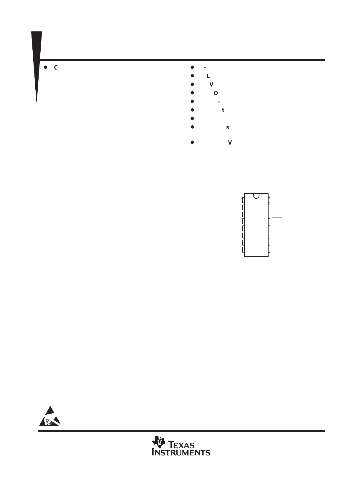
D
Complete PCM Codec and Filtering
Systems Include:
– Transmit High-Pass and Low-Pass
Filtering
– Receive Low-Pass Filter With (sin x)/x
Correction
– Active RC Noise Filters
– µ-Law or A-Law Compatible Coder and
Decoder
– Internal Precision Voltage Reference
– Serial I/O Interface
– Internal Autozero Circuitry
D
µ-Law . . . TP3054A and TP13054A
D
A-Law . . . TP3057A and TP13057A
D
±5-V Operation
D
Low Operating Power...50 mW Typ
D
Power-Down Standby Mode...3 mW Typ
D
Automatic Power Down
D
TTL- or CMOS-Compatible Digital Interface
D
Maximizes Line Interface Card Circuit
Density
D
Improved Versions of National
Semiconductor TP3054, TP3057, TP3054-X,
TP3057-X
description
The TP3054A, TP3057A, TP13054A, and
TP13057A are comprised of a single-chip PCM
codec (pulse code-modulated encoder and
decoder) and PCM line filter. These devices
provide all the functions required to interface a
full-duplex (2-wire) voice telephone circuit with a
TDM (time-division-multiplexed) system. These
devices are pin-for-pin compatible with the
National Semiconductor TP3054A and TP3057A,
respectively. Primary applications include:
• Line interface for digital transmission and
switching of T1 carrier, PABX, and central
office telephone systems
• Subscriber line concentrators
• Digital-encryption systems
• Digital voice-band data-storage systems
• Digital signal processing
These devices are designed to perform the transmit encoding (A/D conversion) and receive decoding (D/A
conversion) as well as the transmit and receive filtering functions in a PCM system. They are intended to be
used at the analog termination of a PCM line or trunk. The devices require two transmit and receive master
clocks that may be asynchronous (1.536 MHz, 1.544 MHz, or 2.048 MHz), transmit and receive data clocks that
are synchronous with the master clock (but can vary from 64 kHz to 2.048 MHz), and transmit and receive
frame-sync pulses. The TP3054A, TP3057A, TP13054A, and TP13057A provide the band-pass filtering of the
analog signals prior to encoding and after decoding of voice and call progress tones. The TP3057A and
TP13057A contain patented circuitry to achieve low transmit channel idle noise and are not recommended for
applications in which the composite signals on the transmit side are below –55 dBm0.
The TP3054A and TP3057A are characterized for operation from 0°C to 70°C. The TP13054A and TP13057A
are characterized for operation from –40°C to 85°C.
These devices have limited built-in ESD protection. The leads should be shorted together or the device placed in conductive foam
during storage or handling to prevent electrostatic damage to the MOS gates.
Copyright 1996, Texas Instruments Incorporated
PRODUCTION DATA information is current as of publication date.
Products conform to specifications per the terms of Texas Instruments
standard warranty. Production processing does not necessarily include
testing of all parameters.
1
2
3
4
5
6
7
8
16
15
14
13
12
11
10
9
V
BB
ANLG GND
VFRO
V
CC
FSR
DR
BCLKR/CLKSEL
MCLKR/PDN
VFXI+
VFXI–
GSX
TSX
FSX
DX
BCLKX
MCLKX
DW OR N PACKAGE
(TOP VIEW)
Page 2
TP3054A, TP3057A, TP13054A, TP13057A
MONOLITHIC SERIAL INTERFACE
COMBINED PCM CODEC AND FILTER
SCTS026C – SEPTEMBER 1992 – REVISED JUL Y 1996
2
POST OFFICE BOX 655303 • DALLAS, TEXAS 75265
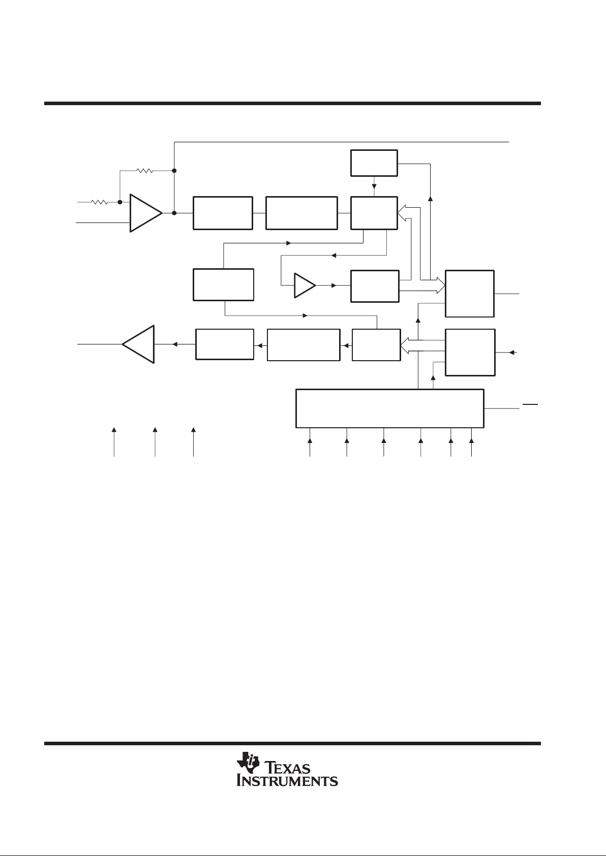
functional block diagram
R2
GSX
14
VBBANLG GNDV
CC
412
–5 V
FSX
5 V
9 8 10 7 125
MCLKX MCLKR/
PDN
BCLKX BCLKR/
CLKSEL
FSR
TSX
13
Power
Amplifier
Timing and Control
DR
6
CLK
Receive
Regulator
S/H
DAC
RC Active
Filter
11
DX
OE
Transmit
Regulator
A/D
Control
Logic
Comparator
Voltage
Reference
Autozero
Logic
S/H
DAC
SwitchedCapacitor
Band-Pass Filter
RC
Active Filter
3
VFRO
+
–
VFXI+
16
R1
15
VFXI–
Analog
Input
SwitchedCapacitor
Low-Pass Filter
Page 3
TP3054A, TP3057A, TP13054A, TP13057A
MONOLITHIC SERIAL INTERFACE
COMBINED PCM CODEC AND FILTER
SCTS026C – SEPTEMBER 1992 – REVISED JUL Y 1996
3
POST OFFICE BOX 655303 • DALLAS, TEXAS 75265
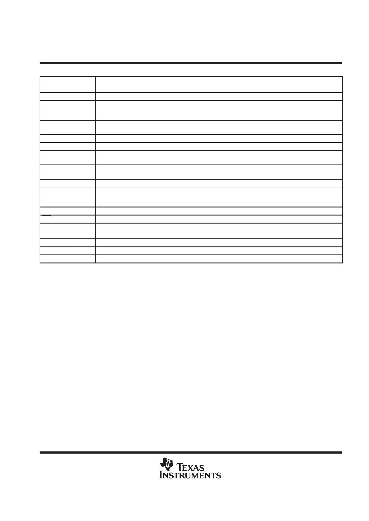
Terminal Functions
TERMINAL
NAME NO.
DESCRIPTION
ANLG GND 2 Analog ground. All signals are referenced to ANLG GND.
BCLKR/CLKSEL 7 The bit clock that shifts data into DR after the FSR leading edge. May vary from 64 kHz to 2.048 MHz. Alternately,
BCLKR/CLKSEL can be a logic input that selects either 1.536 MHz/1.544 MHz or 2.048 MHz for the master clock in
the synchronous mode. BCLKX is used for both transmit and receive directions (see Table 1).
BCLKX 10 The bit clock that shifts out the PCM data on DX. May vary from 64 kHz to 2.048 MHz, but must be synchronous with
MCLKX.
DR 6 Receive data input. PCM data is shifted into DR following the FSR leading edge.
DX 11 The 3-state PCM data output that is enabled by FSX.
FSR 5 Receive-frame sync pulse input that enables BCLKR to shift PCM data in DR. FSR is an 8-kHz pulse train (see
Figures 1 and 2 for timing details).
FSX 12 Transmit-frame sync pulse that enables BCLKX to shift out the PCM data on DX. FSX is an 8-kHz pulse train (see
Figures 1 and 2 for timing details).
GSX 14 Analog output of the transmit input amplifier. GSX is used to externally set gain.
MCLKR/PDN 8 Receive master clock (must be 1.536 MHz, 1.544 MHz, or 2.048 MHz). May be synchronous with MCLKX, but should
be synchronous with MCLKX for best performance. When MCLKR is connected continuously low, MCLKX is selected
for all internal timing. When MCLKR is connected continuously high, the device is powered down.
MCLKX 9 Transmit master clock (must be 1.536 MHz, 1.544 MHz, or 2.048 MHz). May be asynchronous with MCLKR
TSX 13 Open-drain output that pulses low during the encoder time slot
V
BB
1 Negative power supply. VBB = –5 V ±5%
V
CC
4 Positive power supply. VCC = 5 V ±5%
VFRO 3 Analog output of the receive filter
VFXI+ 16 Noninverting input of the transmit input amplifier
VFXI– 15 Inverting input of the transmit input amplifier
Page 4
TP3054A, TP3057A, TP13054A, TP13057A
MONOLITHIC SERIAL INTERFACE
COMBINED PCM CODEC AND FILTER
SCTS026C – SEPTEMBER 1992 – REVISED JUL Y 1996
4
POST OFFICE BOX 655303 • DALLAS, TEXAS 75265
absolute maximum ratings over operating free-air temperature range (unless otherwise noted)†
Supply voltage, VCC (see Note 1) 7 V. . . . . . . . . . . . . . . . . . . . . . . . . . . . . . . . . . . . . . . . . . . . . . . . . . . . . . . . . . . . .
Supply voltage, V
BB
(see Note 1) –7 V. . . . . . . . . . . . . . . . . . . . . . . . . . . . . . . . . . . . . . . . . . . . . . . . . . . . . . . . . . . .
Voltage range at any analog input or output V
CC
+0.3 V to VBB –0.3 V. . . . . . . . . . . . . . . . . . . . . . . . . . . . . . .
Voltage range at any digital input or output V
CC
+0.3 V to ANLG GND –0.3 V. . . . . . . . . . . . . . . . . . . . . . . . . .
Continuous total dissipation See Dissipation Rating Table. . . . . . . . . . . . . . . . . . . . . . . . . . . . . . . . . . . . . . . . . . .
Operating free-air temperature range: TP3054A, TP3057A 0°C to 70°C. . . . . . . . . . . . . . . . . . . . . . . . . . . . . . .
TP13054A, TP13057A –40°C to 85°C. . . . . . . . . . . . . . . . . . . . . . . . . .
Storage temperature range –65°C to 150°C. . . . . . . . . . . . . . . . . . . . . . . . . . . . . . . . . . . . . . . . . . . . . . . . . . . . . . . .
Lead temperature 1,6 mm (1/16 inch) from case for 10 seconds: DW or N package 260°C. . . . . . . . . . . . . . .
†
Stresses beyond those listed under “absolute maximum ratings” may cause permanent damage to the device. These are stress ratings only, and
functional operation of the device at these or any other conditions beyond those indicated under “recommended operating conditions” is not
implied. Exposure to absolute-maximum-rated conditions for extended periods may affect device reliability.
NOTE 1: All voltages are with respect to GND.
DISSIPATION RATING TABLE
PACKAGE
TA ≤ 25°C
POWER RATING
DERATING FACTOR
ABOVE TA = 25°C
TA = 70°C
POWER RATING
TA = 85°C
POWER RATING
DW 1025 mW 8.2 mW/°C 656 mW 533 mW
N 1150 mW 9.2 mW/°C 736 mW 598 mW
recommended operating conditions (see Note 2)
MIN NOM MAX UNIT
Supply voltage, V
CC
4.75 5 5.25 V
Supply voltage, V
BB
–4.75 –5 –5.25 V
High-level input voltage, V
IH
2.2 V
Low-level input voltage, V
IL
0.6 V
Common-mode input voltage range, V
ICR
‡
±2.5 V
Load resistance, GSX, R
L
10 kΩ
Load capacitance, GSX, C
L
50 pF
p
p
TP3054A, TP3057A 0 70
°
Operating free-air temperature, T
A
TP13054A, TP13057A –40 85
°C
‡
Measured with CMRR > 60 dB.
NOTE 2: To avoid possible damage to these CMOS devices and resulting reliability problems, the power-up procedure described in the device
power-up sequence paragraphs later in this document should be followed.
electrical characteristics over recommended ranges of supply voltage operating free-air
temperature range (unless otherwise noted)
supply current
TP305xA TP1305xA
PARAMETER
TEST CONDITIONS
MIN TYP‡MAX MIN TYP‡MAX
UNIT
pp
Power down
0.5 1 0.5 1.2
ICCSupply current from V
CC
Active
No load
6 9 6 10
mA
pp
Power down
0.5 1 0.5 1.2
IBBSupply current from V
BB
Active
No load
6 9 6 10
mA
Page 5
TP3054A, TP3057A, TP13054A, TP13057A
MONOLITHIC SERIAL INTERFACE
COMBINED PCM CODEC AND FILTER
SCTS026C – SEPTEMBER 1992 – REVISED JUL Y 1996
5
POST OFFICE BOX 655303 • DALLAS, TEXAS 75265
electrical characteristics at VCC = 5 V ±5%, V
BB
= – 5 V ± 5%, GND at 0 V, T
A
= 25°C (unless
otherwise noted)
digital interface
PARAMETER TEST CONDITIONS MIN MAX UNIT
V
OH
High-level output voltage DX IH = -3.2 mA 2.4 V
p
DX IL = 3.2 mA 0.4
VOLLow-level output voltage
TSX IL = 3.2 mA, Drain open 0.4
V
I
IH
High-level input current VI = VIH to V
CC
±10 µA
I
IL
Low-level input current All digital inputs VI = GND to V
IL
±10 µA
I
OZ
Output current in high-impedance state DX VO = GND to V
CC
±10 µA
analog interface with transmit amplifier input
PARAMETER TEST CONDITIONS MIN TYP†MAX UNIT
I
I
Input current VFXI+ or VFXI – VI = –2.5 V to 2.5 V ±200 nA
r
i
Input resistance VFXI+ or VFXI – VI = –2.5 V to 2.5 V 10 MΩ
r
o
Output resistance Closed loop, Unity gain 1 3 Ω
Output dynamic range GSX RL ≥ 10 kΩ ±2.8 V
A
V
Open-loop voltage amplification VFXI+ to GSX 5000
B
I
Unity-gain bandwidth GSX 1 2 MHz
V
IO
Input offset voltage VFXI+ or VFXI – ±20 mV
CMRR Common-mode rejection ratio 60 dB
K
SVR
Supply-voltage rejection ratio 60 dB
†
All typical values are at VCC = 5 V, VBB = –5 V , and TA = 25
°C.
analog interface with receive filter
PARAMETER TEST CONDITIONS MIN TYP†MAX UNIT
Output resistance VFRO 1 3 Ω
Load resistance VFRO = ±2.5 V 600 Ω
Load capacitance VFRO to GND 500 pF
Output dc offset voltage VFRO to GND ±200 mV
†
All typical values are at VCC = 5 V, VBB = –5 V , and TA = 25°C.
Page 6
TP3054A, TP3057A, TP13054A, TP13057A
MONOLITHIC SERIAL INTERFACE
COMBINED PCM CODEC AND FILTER
SCTS026C – SEPTEMBER 1992 – REVISED JUL Y 1996
6
POST OFFICE BOX 655303 • DALLAS, TEXAS 75265
timing requirements
PARAMETER TEST CONDITIONS MIN TYP†MAX UNIT
f
clock(M)
Frequency of master clock
MCLKX and
MCLKR
Depends on the device used and
BCLKX/CLKSEL
1.536
1.544
2.048
MHz
f
clock(B)
Frequency of bit clock, transmit BCLKX 64 2048 kHz
t
w1
Pulse duration, MCLKX and MCLKR high 160 ns
t
w2
Pulse duration, MCLKX and MCLKR low 160 ns
t
r1
Rise time of master clock
MCLKX and
MCLKR
50 ns
t
f1
Fall time of master clock
MCLKX and
MCLKR
Measured from 20% to 80%
50 ns
t
r2
Rise time of bit clock, transmit BCLKX
50 ns
t
f2
Fall time of bit clock, transmit BCLKX
Measured from 20% to 80%
50 ns
t
su1
Setup time, BCLKX high (and FSX in long-frame sync
mode) before MCLKX↓
First bit clock after the leading
edge of FSX
100 ns
t
w3
Pulse duration, BCLKX and BCLKR high VIH = 2.2 V 160 ns
t
w4
Pulse duration, BCLKX and BCLKR low VIL = 0.6 V 160 ns
t
h1
Hold time, frame sync low after bit clock low
(long frame only)
0 ns
t
h2
Hold time, BCLKX high after frame sync↑
(short frame only)
0 ns
t
su2
Setup time, frame sync high before bit clock↓
(long frame only)
80 ns
t
d1
Delay time, BCLKX high to data valid
Load = 150 pF plus 2 LSTTL loads
‡
0 140 ns
t
d2
Delay time, BCLKX high to TSX low
Load = 150 pF plus 2 LSTTL loads
‡
140 ns
t
d3
Delay time, BCLKX (or 8 clock FSX in long frame only)
low to data output disabled
50 165 ns
t
d4
Delay time, FSX or BCLKX high to data valid (long
frame only)
CL = 0 pF to 150 pF 20 165 ns
t
su3
Setup time, DR valid before BCLKR↓ 50 ns
t
h3
Hold time, DR valid after BCLKR or BCLKX↓ 50 ns
t
su4
Setup time, FSR or FSX high before BCLKR or
BCLKR↓
Short-frame sync pulse (1 or 2 bit
clock periods long) (see Note 3)
50 ns
t
h4
Hold time, FSX or FSR high after BCLKX or BCLKR↓
Short-frame sync pulse (1 or 2 bit
clock periods long) (see Note 3)
100 ns
t
h5
Hold time, frame sync high after bit clock↓
Long-frame sync pulse
(from 3 to 8 bit clock periods long)
100 ns
t
w5
Minimum pulse duration of the frame sync pulse
(low level)
64 kbps operating mode 160 ns
†
All typical values are at VCC = 5 V, VBB = –5 V , and TA = 25°C.
‡
Nominal input value for an LSTTL load is 18 kΩ.
NOTE 3: For short-frame sync timing, FSR and FSX must go high while their respective bit clocks are high.
Page 7

TP3054A, TP3057A, TP13054A, TP13057A
MONOLITHIC SERIAL INTERFACE
COMBINED PCM CODEC AND FILTER
SCTS026C – SEPTEMBER 1992 – REVISED JUL Y 1996
7
POST OFFICE BOX 655303 • DALLAS, TEXAS 75265
operating characteristics, over operating free-air temperature range, V
CC
= 5 V ±5%,
V
BB
= –5 V±5%, GND at 0 V , V
I
= 1.2276 V , f = 1.02 kHz, transmit input amplifier connected for unity
gain, noninverting (unless otherwise noted)
filter gains and tracking errors
PARAMETER TEST CONDITIONS
‡
MIN TYP†MAX UNIT
p
TP3054A, TP13054A 3.17 dBm0 2.501
Maximum peak transmit overload level
TP3057A, TP13057A 3.14 dBm0 2.492
V
Transmit filter gain, absolute (at 0 dBm0) TA = 25°C – 0.15 0.15 dB
f = 16 Hz –40
f = 50 Hz –30
f = 60 Hz –26
f = 200 Hz –1.8 –0.1
f = 300 Hz to 3000 Hz –0.15 0.15
Transmit filter gain, relative to absolute
f = 3300 Hz –0.35 0.05
dB
f = 3400 Hz –0.8 0
f = 4000 Hz –14
f ≥ 4600 Hz (measure response from
0 Hz to 4000 Hz)
–32
Absolute transmit gain variation with temperature and supply
voltage
Relative to absolute transmit gain –0.1 0.1 dB
Sinusoidal test method,
Reference level = –10 dBm0
Transmit gain tracking error with level
3 dBm0 ≥ input level ≥ –40 dBm0 ±0.2 dB
gg
–40 dBm0 > input level ≥ –50 dBm0 ±0.4
–50 dBm0 > input level ≥ –55 dBm0 ±0.8
Receive filter gain, absolute (at 0 dBm0)
Input is digital code sequence for
0-dBm0 signal, TA = 25°C
–0.15 0.15 dB
f = 0 Hz to 3000 Hz, TA = 25°c –0.15 0.15
f = 3300 Hz –0.35 0.05
Receive filter gain, relative to absolute
f = 3400 Hz –0.8 0
dB
f = 4000 Hz –14
Absolute receive gain variation with temperature and supply
voltage
TA = full range, See Note 4 –0.1 0.1 dB
Sinusoidal test method; reference
input PCM code corresponds to an
ideally encoded –10 dBm0 signal
Receive gain tracking error with level
3 dBm0 ≥ input level ≥ –40 dBm0 ±0.2
–40 dBm0 > input level ≥ –50 dBm0 ±0.4
–50 dBm0 > input level ≥ –55 dBm0 ±0.8
Receive output drive voltage RL = 10 kΩ ±2.5 V
-
Pseudo-noise test method; reference
input PCM code corresponds to an
ideally encoded –10 dBm0 signal
Transmit and receive gain tracking error with level (A law
,
CCITT C 712)
3 dBm0 ≥ input level ≥ –40 dBm0 ±0.25
dB
)
–40 dBm0 > input level ≥ –50 dBm0 ±0.3
–50 dBm0 > input level ≥ –55 dBm0 ±0.45
†
All typical values are at VCC = 5 V, VBB = –5 V , and TA = 25°C.
‡
Absolute rms signal levels are defined as follows: VI = 1.2276 V = 0 dBm0 = 4 dBm at f = 1.02 kHz with RL = 600 Ω.
NOTE 4: Full range for the TP3054A and TP3057A is 0°C to 70°C. Full range for the TP13054A and TP13057A is –40°C to 85°C.
Page 8

TP3054A, TP3057A, TP13054A, TP13057A
MONOLITHIC SERIAL INTERFACE
COMBINED PCM CODEC AND FILTER
SCTS026C – SEPTEMBER 1992 – REVISED JUL Y 1996
8
POST OFFICE BOX 655303 • DALLAS, TEXAS 75265
envelope delay distortion with frequency
PARAMETER TEST CONDITIONS MIN TYP†MAX UNIT
Transmit delay, absolute (at 0 dBm0) f = 1600 Hz 290 315 µs
f = 500 Hz to 600 Hz 195 220
f = 600 Hz to 800 Hz 120 145
f = 800 Hz to 1000 Hz 50 75
Transmit delay, relative to absolute
f = 1000 Hz to 1600 Hz 20 40
µs
f = 1600 Hz to 2600 Hz 55 75
f = 2600 Hz to 2800 Hz 80 105
f = 2800 Hz to 3000 Hz 130 155
Receive delay, absolute (at 0 dBm0) f = 1600 Hz 180 200 µs
f = 500 Hz to 1000 Hz –40 –25
f = 1000 Hz to 1600 Hz –30 –20
Receive delay, relative to absolute
f = 1600 Hz to 2600 Hz 70 90
µs
f = 2600 Hz to 2800 Hz 100 125
f = 2800 Hz to 3000 Hz 140 175
noise
PARAMETER TEST CONDITIONS MIN TYP†MAX UNIT
Transmit noise, C-message weighted
TP3054A,
TP13054A
VFXI = 0 V 9 14 dBrnC0
Transmit noise, psophometric weighted
(see Note 5)
TP3057A,
TP13057A
VFXI = 0 V –78 –75 dBm0p
Receive noise, C-message weighted
TP3054A,
TP13054A
PCM code equals alternating positive
and negative zero
2 4 dBrnC0
Receive noise, psophometric weighted
TP3057A,
TP13057A
PCM code equals positive zero –86 –83 dBm0p
Noise, single frequency
VFXI+ = 0 V, f = 0 kHz to 100 kHz,
Loop-around measurement
–53 dBm0
†
All typical values are at VCC = 5 V, VBB = –5 V , and TA = 25°C.
NOTE 5: Measured by extrapolation from the distortion test result. This parameter is achieved through use of patented circuitry and is not
recommended for applications in which the composite signals on the transmit side are below –55 dBm0.
Page 9

TP3054A, TP3057A, TP13054A, TP13057A
MONOLITHIC SERIAL INTERFACE
COMBINED PCM CODEC AND FILTER
SCTS026C – SEPTEMBER 1992 – REVISED JUL Y 1996
9
POST OFFICE BOX 655303 • DALLAS, TEXAS 75265
power supply rejection
PARAMETER TEST CONDITIONS MIN MAX UNIT
A-law 38 dB
Positive power-supply rejection, transmit
VCC = 5 V + 100 mVrms,
f
= 0 Hz to 4 kHz
µ-law 38 dBC
†
VFXI+ = –50 dBm0
f = 4 kHz to 50 kHz 40 dB
A-law 35 dB
Negative power-supply rejection, transmit
VBB = –5 V + 100 mVrms,
–
f
= 0 Hz to 4 kHz
µ-law 35 dBC
†
VFXI+ = –50 dBm0
f = 4 kHz to 50 kHz 40 dB
A-law 40 dB
Positive power-supply rejection, receive
PCM code equals positive zero,
f
= 0 Hz to 4 kHz
µ-law 40 dBC
†
V
CC
= 5 V +
100 mVrms
f = 4 kHz to 50 kHz 40 dB
A-law 38 dB
Negative power-supply rejection, receive
PCM code equals positive zero,
f
= 0 Hz to 4 kHz
µ-law 38 dBC
†
V
BB
= –5 V +
100 mVrms
f = 4 kHz to 50 kHz 40 dB
0 dBm0, 300-Hz to 3400-Hz input applied to DR (measure individual
image signals at VFRO)
–30 dB
Spurious out-of-band signals at the
p
f = 4600 Hz to 7600 Hz –33
channel output (VFRO)
f = 7600 Hz to 8400 Hz –40
dB
f = 8400 Hz to 100kHz –40
distortion
PARAMETER TEST CONDITIONS MIN MAX UNIT
Level = 3 dBm0 33
Level = 0 dBm0 to -30 dBm0 36
Transmit 29
Si
gnal-to-distortion ratio, transmit or receive half-channe
l
‡
Level
= –40
dBm0
Receive 30
dBC
†
Transmit 14
Level
= –55
dBm0
Receive 15
Single-frequency distortion products, transmit –46 dB
Single-frequency distortion products, receive –46 dB
Intermodulation distortion
Loop-around measurement,
VFXI+ = –4 dBm0 to –21 dBm0,
Two frequencies in the range of 300 Hz to 3400 Hz
–41 dB
Level = –3 dBm0 33
Level = –6 dBm0 to –27 dBm0 36
Signal-to-distortion ratio, transmit half-channel (A-law)
Level = –34 dBm0 33.5
dB
(CCITT G.714)
§
Level = –40 dBm0 28.5
Level = –55 dBm0 13.5
Level = –3 dBm0 33
Level = –6 dBm0 to –27 dBm0 36
Signal-to-distortion ratio, receive half-channel (A-law)
Level = –34 dBm0 34.2
dB
(CCITT G.714)
§
Level = –40 dBm0 30
Level = –55 dBm0 15
†
The unit dBC applies to C-message weighting.
‡
Sinusoidal test method (see Note 6)
§
Pseudo-noise test method
NOTE 6: The TP3054A and TP13054A are measured using a C-message weighted filter. The TP3057A and TP13057A are measured using a
psophometric weighted filter.
Page 10

TP3054A, TP3057A, TP13054A, TP13057A
MONOLITHIC SERIAL INTERFACE
COMBINED PCM CODEC AND FILTER
SCTS026C – SEPTEMBER 1992 – REVISED JUL Y 1996
10
POST OFFICE BOX 655303 • DALLAS, TEXAS 75265
crosstalk
PARAMETER TEST CONDITIONS MIN TYP†MAX UNIT
Crosstalk, transmit to receive f = 300 Hz to 3000 Hz, DR at steady PCM code –90 –75 dB
Crosstalk, receive to transmit (see Note 7) VFXI = 0 V, f = 300 Hz to 3000 Hz –90 –75 dB
†
All typical values are at VCC = 5 V, VBB = –5 V , and TA = 25°C.
NOTE 7: Receive-to-transmit crosstalk is measured with a – 50 dBm0 activation signal applied at VFXI+.
PARAMETER MEASUREMENT INFORMATION
1 8765432
87654321
87654321
t
h2
t
h4
t
su4
t
h3
t
h3
t
su3
87654321
BCLKR
FSR
DR
FSX
DX
t
d3
t
d1
t
h4
t
su4
t
h2
BCLKX
MCLKX
MCLKR
t
w1
t
su1
f
clock(M)
t
w2
t
f1
t
r1
t
d3
t
d2
TSX
80%
20%
80%
20%
20%
80%
20%
80%
20%
80%
20%
80% 80%
20%
80%
20%
80%
20%
80%
20%
80%
20%
20%
80%
Figure 1. Short-Frame Sync Timing
Page 11

TP3054A, TP3057A, TP13054A, TP13057A
MONOLITHIC SERIAL INTERFACE
COMBINED PCM CODEC AND FILTER
SCTS026C – SEPTEMBER 1992 – REVISED JUL Y 1996
11
POST OFFICE BOX 655303 • DALLAS, TEXAS 75265
PARAMETER MEASUREMENT INFORMATION
t
h3
t
h3
t
su3
t
h5
t
su2
t
h1
t
d3
t
d3
t
d1
t
d4
t
d4
DR
FSR
BCLKR
DX
FSX
987654321
t
h5
f
clock(B)
t
su2
t
h1
BCLKX
t
w4
t
w3
t
f2
t
r2
t
su1
t
su1
MCLKX
MCLKR
t
w2
f
clock(M)
t
f1
t
w1
t
r1
78654321
123456 87
20%
80%80%
20%
80%
20%
80%
80%
20%
80%
20%
20%
80%
20%
20%
20%
80% 80%
20%
20%
80%
20%
80%
20%
80%
80%
t
w4
t
w3
80%
Figure 2. Long-Frame Sync Timing
Page 12

TP3054A, TP3057A, TP13054A, TP13057A
MONOLITHIC SERIAL INTERFACE
COMBINED PCM CODEC AND FILTER
SCTS026C – SEPTEMBER 1992 – REVISED JUL Y 1996
12
POST OFFICE BOX 655303 • DALLAS, TEXAS 75265
PRINCIPLES OF OPERATION
system reliability and design considerations
TP305xA, TP1305xA system reliability and design considerations are described in the following paragraphs.
latch-up
Latch-up is possible in all CMOS devices. It is caused by the firing of a parasitic SCR that is present due to the
inherent nature of CMOS. When a latch-up occurs, the device draws excessive amounts of current and will
continue to draw heavy current until power is removed. Latch-up can result in permanent damage to the device
if supply current to the device is not limited.
Even though the TP305xA and TP1305xA are heavily protected against latch-up, it is still possible to cause
latch-up under certain conditions in which excess current is forced into or out of one or more terminals. Latch-up
can occur when the positive supply voltage drops momentarily below ground, when the negative supply voltage
rises momentarily above ground, or possibly if a signal is applied to a terminal after power has been applied
but before the ground is connected. This can happen if the device is hot-inserted into a card with the power
applied, or if the device is mounted on a card that has an edge connector and the card is hot-inserted into a
system with the power on.
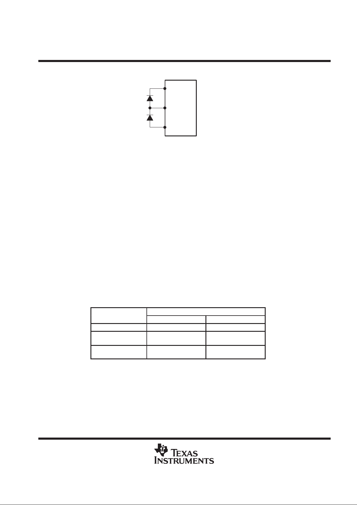
To help ensure that latch-up does not occur, it is considered good design practice to connect a reverse-biased
Schottky diode (with a forward voltage drop of less than or equal to 0.4 V – 1N571 1 or equivalent) between the
power supply and GND (see Figure 3). If it is possible that a TP305xA- or TP1305xA-equipped card that has
an edge connector could be hot-inserted into a powered-up system, it is also important to ensure that the ground
edge connector traces are longer than the power and signal traces so that the card ground is always the first
to make contact.
device power-up sequence
Latch-up can also occur if a signal source is connected without the device being properly grounded. A signal
applied to one terminal could then find a ground through another signal terminal on the device. T o ensure proper
operation of the device and as a safeguard against this sort of latch-up, it is recommended that the following
power-up sequence always be used:
1. Ensure that no signals are applied to the device before the power-up sequence is complete.
2. Connect GND.
3. Apply V
BB
(most negative voltage).
4. Apply V
CC
(most positive voltage).
5. Force a power down condition in the device.
6. Connect clocks.
7. Release the power down condition.
8. Apply FS synchronization pulses.
9. Apply the signal inputs.
When powering down the device, this procedure should be followed in the reverse order.
Page 13
TP3054A, TP3057A, TP13054A, TP13057A
MONOLITHIC SERIAL INTERFACE
COMBINED PCM CODEC AND FILTER
SCTS026C – SEPTEMBER 1992 – REVISED JUL Y 1996
13
POST OFFICE BOX 655303 • DALLAS, TEXAS 75265
PRINCIPLES OF OPERATION
V
CC
DGND
V
BB
Figure 3. Latch-Up Protection Diode Connection
internal sequencing
Power-on reset circuitry initializes the TP3054A, TP3057A, TP13054A, and TP13057A devices when power
is first applied, placing it into the power-down mode. DX and VFRO outputs go into high-impedance states and
all nonessential circuitry is disabled. A low level or clock applied to MCLKR/PDN powers up the device and
activates all circuits. DX, a 3-state PCM data output, remains in the high-impedance state until the arrival of the
second FSX pulse.
synchronous operation
For synchronous operation, a clock is applied to MCLKX. MCLKR/PDN is used as a power-down control. A low
level on MCLKR powers up the device and a high level powers it down. In either case, MCLKX is selected as
the master clock for both receive and transmit direction. BCLKX must also have a bit clock applied to it. The
selection of the proper internal divider for a master-clock frequency of 1.536 MHz, 1.544 MHz, or 2.048 MHz
can be done via BCLKR/CLKSEL. The device automatically compensates for the 193rd clock pulse of each
frame.
A fixed level on BCLKR/CLKSEL selects BCLKX as the bit clock for both the transmit and receive directions.
T able 1 indicates the frequencies of operation that can be selected depending on the state of BCLKR/CLKSEL.
In the synchronous mode, BCLKX may be in the range from 64 kHz to 2.048 MHz but must be synchronous
with MCLKX.
Table 1. Selection of Master-Clock Frequencies
MASTER-CLOCK FREQUENCY SELECTED
BCLKR/CLKSEL
TP13054A, TP3054A TP13057A, TP3057A
Clock Input 1.536 MHz or 1.544 MHz 2.048 MHz
Logic Input L
(sync mode only)
2.048 MHz 1.536 MHz or 1.544 MHz
Logic Input H (open)
(sync mode only)
1.536 MHz or 1.544 MHz 2.048 MHz
The encoding cycle begins with each FSX pulse and the PCM data from the previous cycle is shifted out of the
enabled DX output on the rising edge of BCLKX. After eight bit-clock periods, the 3-state DX output is returned
to the high-impedance state. With an FSR pulse, PCM data is latched via DR on the falling edge of BCLKX (or
BCLKR, if running). FSX and FSR must be synchronous with MCLKX and MCLKR.
Page 14

TP3054A, TP3057A, TP13054A, TP13057A
MONOLITHIC SERIAL INTERFACE
COMBINED PCM CODEC AND FILTER
SCTS026C – SEPTEMBER 1992 – REVISED JUL Y 1996
14
POST OFFICE BOX 655303 • DALLAS, TEXAS 75265
PRINCIPLES OF OPERATION
asynchronous operation
For asynchronous operation, separate transmit and receive clocks can be applied. MCLKX and MCLKR must
be 2.048 MHz for the TP3057A and TP13057A, 1.536 MHz or 1.544 MHz for the TP3054A and TP13054A and
need not be synchronous. However, for best performance, MCLKR should be synchronous with MCLKX. This
is easily achieved by applying only static logic levels to MCLKR/PDN. This connects MCLKX to all internal
MCLKR functions. For 1.544-MHz operation, the device compensates for the 193rd clock pulse of each frame.
Each encoding cycle is started with FSX and FSX must be synchronous with MCLKX and BCLKX. Each
decoding cycle is started with FSR and FSR must be synchronous with BCLKR. The logic levels shown in
Table 1 are not valid in the asynchronous mode. BCLKX and BCLKR can operate from 64 kHz to 2.048 MHz.
short-frame sync operation
The device can operate with either a short- or a long-frame sync pulse. On power up, the device automatically
goes into the short-frame mode where both FSX and FSR must be one bit-clock period long with timing
relationships specified in Figure 1. With FSX high during a falling edge of BCLKX, the next rising edge of BCLKX
enables the 3-state output buffer , DX, which outputs the sign bit. The remaining seven bits are clocked out on
the following seven rising edges, and the next falling edge disables DX. With FSR high during a falling edge
of BCLKR (BCLKX in synchronous mode), the next falling edge of BCLKR latches in the sign bit. The following
seven falling edges latch in the seven remaining bits. The short-frame sync pulse may be utilized in either the
synchronous or asynchronous mode.
long-frame sync operation
Both FSX and FSR must be three or more bit-clock periods long to use the long-frame sync mode with timing
relationships as shown in Figure 2. Using the transmit frame sync (FSX), the device detects whether a shortor long-frame sync pulse is being used. For 64-kHz operation, the frame-sync pulse must be kept low for a
minimum of 160 ns. The rising edge of FSX or BCLKX, whichever occurs later, enables the DX 3-state output
buffer. The first bit clocked out is the sign bit. The next seven rising edges of BCLKX edges clock out the
remaining seven bits. The falling edge of BCLKX following the eighth rising edge or FSX going low, whichever
occurs later, disables DX. A rising edge on FSR, the receive-frame sync pulse, causes the PCM data at DR to
be latched in on the next eight falling edges of BCLKR (BCLKX in synchronous mode). The long-frame sync
pulse can be utilized in either the synchronous or asynchronous mode.
transmit section
The transmit section input is an operational amplifier with provision for gain adjustment using two external
resistors. The low noise and wide bandwidth characteristics of these devices provide gains in excess of 20 dB
across the audio passband. The operational amplifier drives a unity-gain filter consisting of an RC active prefilter
followed by an eighth-order switched-capacitor band-pass filter clocked at 256 kHz. The output of this filter
directly drives the encoder sample-and-hold circuit. As per µ-law (TP3054A and TP13054A) or A-law (TP3057A
and TP13057A) coding conventions, the ADC is a companding type. A precision voltage reference provides a
nominal input overload (t
[max]
) of nominally 2.5 V peak. The sampling of the filter output is controlled by the FSX
frame-sync pulse. Then the successive-approximation encoding cycle begins. The 8-bit code is loaded into a
buffer and shifted out through DX at the next FSX pulse. The total encoding delay is approximately 290 µs. Any
offset voltage due to the filters or comparator is cancelled by sign-bit integration.
Page 15

TP3054A, TP3057A, TP13054A, TP13057A
MONOLITHIC SERIAL INTERFACE
COMBINED PCM CODEC AND FILTER
SCTS026C – SEPTEMBER 1992 – REVISED JUL Y 1996
15
POST OFFICE BOX 655303 • DALLAS, TEXAS 75265
PRINCIPLES OF OPERATION
receive section
The receive section consists of an expanding DAC that drives a fifth-order low-pass filter clocked at 256 kHz.
The decoder is µ-law (TP3054A and TP13054A) or A-law (TP3057A and TP13057A) and the fifth-order
low-pass filter corrects for the (sin x)/x attenuation caused by the 8-kHz sample/hold. The filter is followed by
a second-order RC active post-filter/power amplifier capable of driving a 600-Ω load to a level of 7.2 dBm. The
receive section is unity gain. At FSR, the data at DR is clocked in on the falling edge of the next eight BCLKR
(BCLKX) periods. At the end of the decoder time slot, the decoding cycle begins and 10 µs later, the decoder
DAC output is updated. The decoder delay is about 10 µs (decoder update) plus 110 µs (filter delay) plus
62.5 µs (1/2 frame), or a total of approximately 180 µs.
Page 16
TP3054A, TP3057A, TP13054A, TP13057A
MONOLITHIC SERIAL INTERFACE
COMBINED PCM CODEC AND FILTER
SCTS026C – SEPTEMBER 1992 – REVISED JUL Y 1996
16
POST OFFICE BOX 655303 • DALLAS, TEXAS 75265
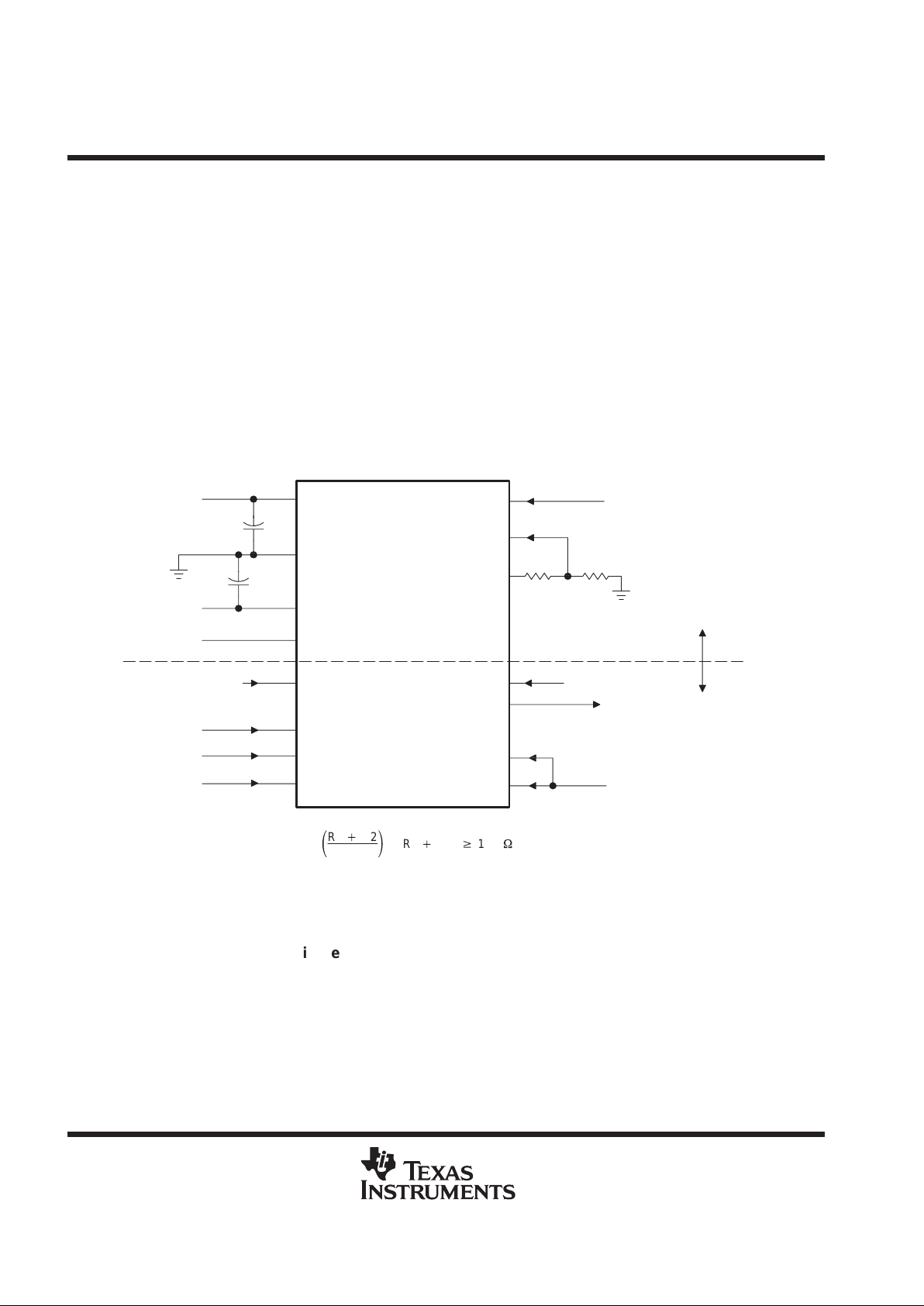
APPLICATION INFORMATION
power supplies
While the pins of the TP1305xA and TP305xA families are well protected against electrical misuse, it is
recommended that the standard CMOS practice be followed ensuring that ground is connected to the device
before any other connections are made. In applications where the printed-circuit board can be plugged into a
hot socket with power and clocks already present, an extra long ground pin in the connector should be used.
All ground connections to each device should meet at a common point as close as possible to ANLG GND. This
minimizes the interaction of ground return currents flowing through a common bus impedance. V
CC
and V
BB
supplies should be decoupled by connecting 0.1-µF decoupling capacitors to this common point. These bypass
capacitors must be connected as close as possible to V
CC
and VBB.
For best performance, the ground point of each codec/filter on a card should be connected to a common card
ground in star formation rather than via a ground bus. This common ground point should be decoupled to V
CC
and VBB with 10-µF capacitors.
BCLKX (2.048 MHz/1.544 MHz)
Data
Out
Digital
Interface
Analog Interface
R2R1
From SLIC
PDN
5 V or GND
Data In
To SLIC
5 V
0.1
µF
0.1
µF
–5 V
MCLKX
BCLKX
DX
FSX
GSX
VFXI–
VFXI+
MCLKR/PDN
BCLKR/CLKSEL
DR
FSR
VFRO
V
CC
ANLG GND
V
BB
NOTE A: Transmit gain = 20 log
1
2
4
3
5
6
7
8
16
15
14
12
11
10
9
TP3054A
TP3057A
TP13054A
TP13057A
ǒ
R1)R2
R2
Ǔ
,
(
R1)R2)w
10 k
W
Figure 4. Typical Synchronous Application
Page 17

IMPORTANT NOTICE
T exas Instruments and its subsidiaries (TI) reserve the right to make changes to their products or to discontinue
any product or service without notice, and advise customers to obtain the latest version of relevant information
to verify, before placing orders, that information being relied on is current and complete. All products are sold
subject to the terms and conditions of sale supplied at the time of order acknowledgement, including those
pertaining to warranty, patent infringement, and limitation of liability.
TI warrants performance of its semiconductor products to the specifications applicable at the time of sale in
accordance with TI’s standard warranty. Testing and other quality control techniques are utilized to the extent
TI deems necessary to support this warranty. Specific testing of all parameters of each device is not necessarily
performed, except those mandated by government requirements.
CERT AIN APPLICATIONS USING SEMICONDUCTOR PRODUCTS MAY INVOLVE POTENTIAL RISKS OF
DEATH, PERSONAL INJURY, OR SEVERE PROPERTY OR ENVIRONMENTAL DAMAGE (“CRITICAL
APPLICATIONS”). TI SEMICONDUCTOR PRODUCTS ARE NOT DESIGNED, AUTHORIZED, OR
WARRANTED TO BE SUITABLE FOR USE IN LIFE-SUPPORT DEVICES OR SYSTEMS OR OTHER
CRITICAL APPLICATIONS. INCLUSION OF TI PRODUCTS IN SUCH APPLICA TIONS IS UNDERST OOD TO
BE FULLY AT THE CUSTOMER’S RISK.
In order to minimize risks associated with the customer’s applications, adequate design and operating
safeguards must be provided by the customer to minimize inherent or procedural hazards.
TI assumes no liability for applications assistance or customer product design. TI does not warrant or represent
that any license, either express or implied, is granted under any patent right, copyright, mask work right, or other
intellectual property right of TI covering or relating to any combination, machine, or process in which such
semiconductor products or services might be or are used. TI’s publication of information regarding any third
party’s products or services does not constitute TI’s approval, warranty or endorsement thereof.
Copyright 1998, Texas Instruments Incorporated
 Loading...