

Page 1
TNETX3270
ThunderSWITCH 24/3 ETHERNET SWITCH
WITH 24 10-MBIT/S PORTS AND 3 10-/100-MBIT/S PORTS
SPWS043B – NOVEMBER 1997 – REVISED APRIL 1999
D
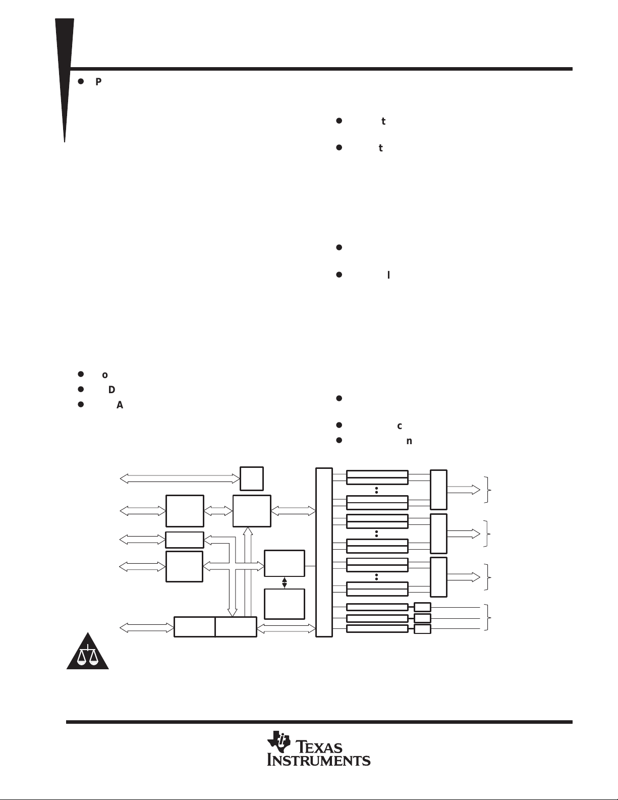
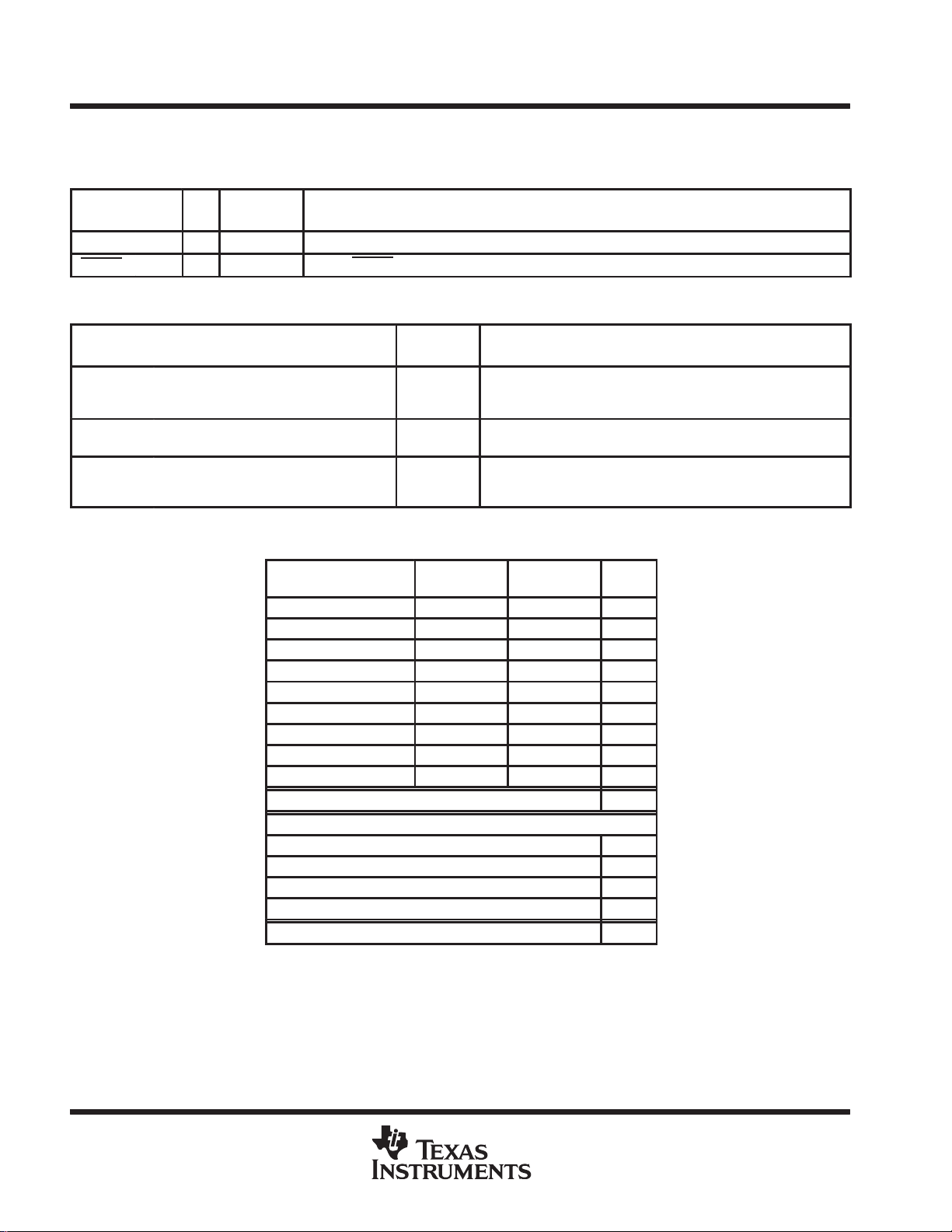
Port Configurations:
Twenty-Four 10-Mbit/s Ports
– Ports Arranged in Three Groups of Eight
Ports in a Multiplexed Interface
– Direct Multiplexer Interface to
TNETE2008
– Full and Half Duplex
– Half-Duplex Collision-Based Flow
Control
– Full-Duplex IEEE Std 802.3x Flow Control
– Interoperable Support for IEEE
Std 802.1Q VLAN
– Speed, Duplex, and Pause
Autonegotiation With Physical Layer
(PHY)
Three 10-/100-Mbit/s Ports
– Direct Interface to TNETE2101
– Full and Half Duplex
– Half-Duplex Collision-Based Flow
Control
– Full-Duplex IEEE Std 802.3x Flow Control
– Interoperable Support for IEEE
Std 802.1Q VLAN
– Pretagging Support
D
Port Trunking and Load Sharing
D
LED Indication of Port Status
D
SDRAM Interface
– Direct Interface to 8-Bit/Word and
16-Bit/Word, 16-Mbit, and 64-Mbit
SDRAMs
– 32-Bit-Wide Data Bus
– Up to 32 Mbytes Supported
– 83.33-MHz SDRAM Clock
– 12-ns (–12) SDRAMs Required
D
Remote Monitoring (RMON) Support –
Groups 1, 2, 3, and 9
D
Direct I/O (DIO) Management Interface
– Eight Bits Wide
– CPU Access to Statistics, Registers, and
Management Information Bases (MIBs)
– Internal Network Management Port
– Forwards Spanning-Tree Packets to CPU
– Serial Media-Independent Interface (MII)
for PHY Control
D
EEPROM Interface for Autoconfiguration
(No CPU Required for Nonmanaged Switch)
D
Internal Address-Lookup/Frame-Routing
Engine
– Interoperable Support for IEEE
Std 802.1Q VLAN
– Supports IEEE Std 802.1D Spanning Tree
– Thirty-Two Assignable Virtual LANs
(VLANs)
– Multiple Forwarding Modes
– 2K Total Addresses Supported
– Port Mirroring
D
IEEE Std 1149.1 (JTAG) Interface (3.3-V
Signals)
D
2.5-V Process With 3.3-V-Drive I/O
D
Packaged in 240-Terminal Plastic Quad
Flatpack
TAP
(JTAG)
SDRAM
Controller
EEPROM
Interface
CPU
Interface
LED
Interface
Please be aware that an important notice concerning availability, standard warranty, and use in critical applications of
Texas Instruments semiconductor products and disclaimers thereto appears at the end of this data sheet.
TI and ThunderSWITCH are trademarks of Texas Instruments Incorporated.
Ethernet is a trademark of Xerox Corporation.
Secure Fast Switching is a trademark of Cabletron Systems, Inc.
Port-trunking and load-sharing algorithms were contributed by Cabletron Systems, Inc. and are derived from, and compatible with, Secure Fast
Switching.
PRODUCTION DATA information is current as of publication date.
Products conform to specifications per the terms of Texas Instruments
standard warranty. Production processing does not necessarily include
testing of all parameters.
Manager
Address
Compare
Queue
Network
Statistics
Logic
Statistics
Storage
MIB
Data Path
Controller (MAC)
Controller (MAC)
Controller (MAC)
Controller (MAC)
Controller (MAC)
Controller (MAC)
Controller (MAC)
Controller (MAC)
Controller (MAC)
Controller (MAC)
Controller (MAC)
Controller (MAC)
Controller (MAC)
Controller (MAC)
Controller (MAC)
MUX
MUX
MUX
MII
MII
MII
Copyright 1999, Texas Instruments Incorporated
Eight Ports
(00–07)
10 Mbit/s
Eight Ports
(08–15)
10 Mbit/s
Eight Ports
(16–23)
10 Mbit/s
Three Ports
(24–26)
10/100 Mbit/s
POST OFFICE BOX 655303 • DALLAS, TEXAS 75265
1
Page 2

TNETX3270
ThunderSWITCH 24/3 ETHERNET SWITCH
WITH 24 10-MBIT/S PORTS AND 3 10-/100-MBIT/S PORTS
SPWS043B – NOVEMBER 1997 – REVISED APRIL 1999
description
The TNETX3270 provides highly integrated switching solutions that allow network designers to lower overall
system costs. Based on Texas Instruments (TI) ThunderSWITCH architecture, the TNETX3270 design
integrates 24 full-duplex 10-Mbit/s ports and 3 full-duplex 10-/100-Mbit/s ports, as well as an address-lookup
engine, all in a single 240-pin package. All ports on the TNETX3270 are designed to support multiple addresses,
cut-through or store-and-forward modes of operation, and VLAN. The 10-/100-Mbit/s ports have
media-independent interface (MII)-compatible interfaces and can be configured to work as MII uplinks to
high-speed switching fabrics. All three of the 10-/100-Mbit/s ports can be logically combined into a single
high-performance uplink channel that can be used to provide up to 600-Mbit/s switch-to-switch connections.
The TNETX3270 incorporates an internal content-addressable memory (CAM) capable of supporting 2,048 end
stations from a single switch. In addition, the device supports 32 user-configurable VLAN-broadcast domains
(IEEE Std 802.1Q), which allows IEEE Std 802.1P priority support interoperability , IEEE Std 802.3X full-duplex
flow control, and a collision-based flow-control scheme. The TNETX3270 also integrates an EEPROM interface
that allows the device to be initialized and configured without the added expense of a CPU. All of these features
on chip greatly reduce the number of external components required to build a switch.
The internal address-lookup engine (IALE) supports up to 2K unicast/multicast and broadcast addresses and
up to 32 IEEE Std 802.1Q VLANs. For interoperability, each port can be programmed as an access port or
non-access port to recognize VLAN tags and transmit frames with VLAN tags to other systems that support
VLAN tagging. The IALE performs destination- and source-address comparisons and forwards unknown
source- and destination-address packets to ports specified via programmable masks.
2
POST OFFICE BOX 655303 • DALLAS, TEXAS 75265
Page 3

WITH 24 10-MBIT/S PORTS AND 3 10-/100-MBIT/S PORTS
Description 2. . . . . . . . . . . . . . . . . . . . . . . . . . . . . . . . . . . . . . . . . . .
PGV Package Terminal Layout 4. . . . . . . . . . . . . . . . . . . . . . . . . .
TNETX3270 Interface Block Diagram 5. . . . . . . . . . . . . . . . . . . .
Terminal Functions 6. . . . . . . . . . . . . . . . . . . . . . . . . . . . . . . . . . . .
DIO Register Groups 13. . . . . . . . . . . . . . . . . . . . . . . . . . . . . . . . .
Interface Description 18. . . . . . . . . . . . . . . . . . . . . . . . . . . . . . . . .
DIO Interface 18. . . . . . . . . . . . . . . . . . . . . . . . . . . . . . . . . . . . . .
Receiving/Transmitting Management Frames 18. . . . . . . .
State of DIO Signals During Hardware Reset 18. . . . . . . .
Network Management Port 19. . . . . . . . . . . . . . . . . . . . . . . .
MII Serial Management Interface (PHY Management) 22. . .
10-Mbit/s and 10-/100-Mbit/s MAC Interface 22. . . . . . . . . . . .
Receive Control 22. . . . . . . . . . . . . . . . . . . . . . . . . . . . . . . . .
Giant (Long) Frames 22. . . . . . . . . . . . . . . . . . . . . . . . . . . . .
Short Frames 22. . . . . . . . . . . . . . . . . . . . . . . . . . . . . . . . . . .
Receive Filtering of Frames 23. . . . . . . . . . . . . . . . . . . . . . .
Data Transmission 23. . . . . . . . . . . . . . . . . . . . . . . . . . . . . . .
Transmit Control 23. . . . . . . . . . . . . . . . . . . . . . . . . . . . . . . .
Adaptive Performance Optimization
(APO) (Transmit Pacing) 23. . . . . . . . . . . . . . . . . . . . . . . . .
Interframe Gap Enforcement 23. . . . . . . . . . . . . . . . . . . . . .
Backoff 23. . . . . . . . . . . . . . . . . . . . . . . . . . . . . . . . . . . . . . . .
Receive Versus Transmit Priority 24. . . . . . . . . . . . . . . . . .
Uplink Pretagging 24. . . . . . . . . . . . . . . . . . . . . . . . . . . . . . .
EEPROM Interface 27. . . . . . . . . . . . . . . . . . . . . . . . . . . . . . . . .
Interaction of EEPROM Load With the SIO Register 28. .
Summary of EEPROM Load Outcomes 28. . . . . . . . . . . . .
Compatibility With Future Device Revisions 28. . . . . . . . .
JTAG Interface 29. . . . . . . . . . . . . . . . . . . . . . . . . . . . . . . . . . . . .
HIGHZ instruction 29. . . . . . . . . . . . . . . . . . . . . . . . . . . . . . .
LED Interface 29. . . . . . . . . . . . . . . . . . . . . . . . . . . . . . . . . . . . . .
Lamp Test 30. . . . . . . . . . . . . . . . . . . . . . . . . . . . . . . . . . . . . .
Multi-LED Display 30. . . . . . . . . . . . . . . . . . . . . . . . . . . . . . .
Hardware Configurations 30. . . . . . . . . . . . . . . . . . . . . . . . . . . . .
10-Mbit/s MAC Interfaces (Ports 00–23) 30. . . . . . . . . . . . . . .
10-/100-Mbit/s MAC Interfaces (Ports 24–26) 34. . . . . . . . . . .
10-/100-Mbit/s Port Configuration 34. . . . . . . . . . . . . . . . . .
10-/100-Mbit/s Port Configuration
in a Nonmanaged Switch 35. . . . . . . . . . . . . . . . . . . . . . . . .
10-/100-Mbit/s Port Configuration
in a Managed Switch 36. . . . . . . . . . . . . . . . . . . . . . . . . . . . .
TNETX3270
ThunderSWITCH 24/3 ETHERNET SWITCH
SPWS043B – NOVEMBER 1997 – REVISED APRIL 1999
Contents
SDRAM Interface 36. . . . . . . . . . . . . . . . . . . . . . . . . . . . . . . . . . . . . .
SDRAM-Type and Quantity Indication 38. . . . . . . . . . . . . . . . .
Initialization 38. . . . . . . . . . . . . . . . . . . . . . . . . . . . . . . . . . . . . . . .
Refresh 38. . . . . . . . . . . . . . . . . . . . . . . . . . . . . . . . . . . . . . . . . . .
Frame Routing 39. . . . . . . . . . . . . . . . . . . . . . . . . . . . . . . . . . . . . . . . . .
VLAN Support 39. . . . . . . . . . . . . . . . . . . . . . . . . . . . . . . . . . . . . . . .
IEEE Std 802.1Q Headers – Reception 40. . . . . . . . . . . . . . . .
IEEE Std 802.1Q Headers – Transmission 40. . . . . . . . . . . . .
Address Maintenance 40. . . . . . . . . . . . . . . . . . . . . . . . . . . . . . .
Spanning-Tree Support 41. . . . . . . . . . . . . . . . . . . . . . . . . . . . . .
Aging Algorithms 41. . . . . . . . . . . . . . . . . . . . . . . . . . . . . . . . . . .
Frame-Routing Determination 41. . . . . . . . . . . . . . . . . . . . . . . .
Port Mirroring 44. . . . . . . . . . . . . . . . . . . . . . . . . . . . . . . . . . . . . .
Port Trunking/Load Sharing 45. . . . . . . . . . . . . . . . . . . . . . . . . .
Flow Control 45. . . . . . . . . . . . . . . . . . . . . . . . . . . . . . . . . . . . . . . . . .
Collision-Based Flow Control 46. . . . . . . . . . . . . . . . . . . . . . . . .
IEEE Std 802.3 Flow Control 46. . . . . . . . . . . . . . . . . . . . . . . . .
Internal Wrap Test 48. . . . . . . . . . . . . . . . . . . . . . . . . . . . . . . . . .
Duplex Wrap Test 49. . . . . . . . . . . . . . . . . . . . . . . . . . . . . . . . . .
Port Mirroring 50. . . . . . . . . . . . . . . . . . . . . . . . . . . . . . . . . . . . . .
Copy to Uplink 50. . . . . . . . . . . . . . . . . . . . . . . . . . . . . . . . . . . . .
Absolute Maximum Ratings 51. . . . . . . . . . . . . . . . . . . . . . . . . . . . . .
Recommended Operating Conditions 51. . . . . . . . . . . . . . . . . . . . .
Electrical Characteristics 51. . . . . . . . . . . . . . . . . . . . . . . . . . . . . . . .
Parameter Measurement Information 52. . . . . . . . . . . . . . . . . . . . . .
Test Measurement 52. . . . . . . . . . . . . . . . . . . . . . . . . . . . . . . . . . . . .
10-Mbit/s Interface (Ports 00–23) 53. . . . . . . . . . . . . . . . . . . . . . . . . .
10-/100-Mbit/s MAC Interface 54. . . . . . . . . . . . . . . . . . . . . . . . . . . . .
SDRAM Interface 56. . . . . . . . . . . . . . . . . . . . . . . . . . . . . . . . . . . . . . . .
DIO/DMA Interface 58. . . . . . . . . . . . . . . . . . . . . . . . . . . . . . . . . . . . . . .
Serial MII Management Interface 60. . . . . . . . . . . . . . . . . . . . . . . . . .
EEPROM Interface 61. . . . . . . . . . . . . . . . . . . . . . . . . . . . . . . . . . . . . . .
LED Interface 62. . . . . . . . . . . . . . . . . . . . . . . . . . . . . . . . . . . . . . . . . . .
Power-Up OSCIN and RESET 63. . . . . . . . . . . . . . . . . . . . . . . . . . . . .
Mechanical Data 64. . . . . . . . . . . . . . . . . . . . . . . . . . . . . . . . . . . . . . . .
POST OFFICE BOX 655303 • DALLAS, TEXAS 75265
3
Page 4
TNETX3270
ThunderSWITCH 24/3 ETHERNET SWITCH
WITH 24 10-MBIT/S PORTS AND 3 10-/100-MBIT/S PORTS
SPWS043B – NOVEMBER 1997 – REVISED APRIL 1999
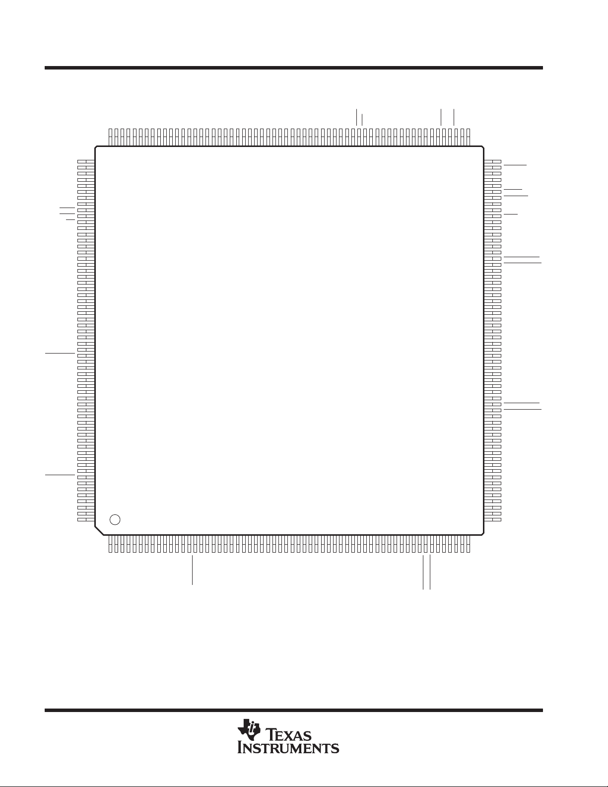
PGV PACKAGE
(TOP VIEW)
DD26
DD27
DD28
V
DD(2.5V)
DD29
DD30
DD31
GND
DCAS
DRAS
DW
V
DD(3.3V)
DCLK
GND
DA00
DA01
V
DD(2.5V)
DA02
DA03
DA04
GND
DA05
DA06
DA07
DA08
DA09
DA10
GND
DA11
DA12
V
DD(2.5V)
DA13
TH0RENEG
GND
TH0TXD0
TH0TXD1
TH0TXD2
TH0TXD3
TH0TXEN
GND
TH0SYNC
TH0CLK
TH0COL
TH0CRS
V
DD(2.5V)
TH0RXDV
TH0RXD0
TH0RXD1
V
DD(3.3V)
TH0RXD2
TH0RXD3
TH0LINK
TH1RENEG
TH1TXD0
GND
TH1TXD1
TH1TXD2
V
DD(2.5V)
TH1TXD3
TH1TXEN
181
182
183
184
185
186
187
188
189
190
191
192
193
194
195
196
197
198
199
200
201
202
203
204
205
206
207
208
209
210
211
212
213
214
215
216
217
218
219
220
221
222
223
224
225
226
227
228
229
230
231
232
233
234
235
236
237
238
239
240
DD25
180
1
DD(2.5V)
DD24VDD23
DD22
GND
DD21
DD20
175
179
178
177
176
174
173
5
2346789
DD15
DD14
167
DD(2.5V)
V
165
166
15
DD13
164
DD(3.3V)
V
DD12
163
162
DD11
161
20
GND
160
DD10
159
DD09
158
DD08
DD07
157
25
156
DD06
GND
155
154
DD05
153
DD04
V
152
DD(2.5V)
DD03
DD02
150
151
149
GND
148
DD01
147
DD00
SRXRDY
145
146
35
STXRDY
SAD1
SAD0
144
143
142
GND
141
40
SINT
140
SRDY
SCS
139
138
V
DD(3.3V)
DD19
DD18
DD17
DD16
V
170
172
171
169
168
10
1112131416171819212223242627282930313233343637383941424344464748495152535456575859
DD(2.5V)
SDATA7
SDATA6
135
137
136
45
GND
134
DD(3.3V)
V
SDATA5
133
132
SDATA4
131
50
SDATA3
130
SDATA2
129
GND
128
SDATA1
127
SDATA0
126
55
DD(2.5V)
SRNW
V
125
124
V
SDMA
123
122
DD(3.3V)
MDCLK
121
120
119
118
117
116
115
114
113
112
111
110
109
108
107
106
105
104
103
102
101
100
99
98
97
96
95
94
93
92
91
90
89
88
87
86
85
84
83
82
81
80
79
78
77
76
75
74
73
72
71
70
69
68
67
66
65
64
63
62
61
60
MDIO
MRESET
V
DD(2.5V)
ECLK
EDIO
RESET
LEDDATA
LEDCLK
OSCIN
TRST
TDI
V
DD(3.3V)
TDO
TMS
TCLK
V
DD(2.5V)
M26FORCE10
M26FORCEHD
M26LINK
M26RXER
GND
M26RXDV
M26RXD3
M26RXD2
M26RXD1
M26RXD0
GND
M26RCLK
M26CRS
V
DD(2.5V)
M26COL
M26TXER
GND
M26TXEN
M26TXD3
M26TXD2
M26TXD1
M26TXD0
M26TCLK
GND
M25FORCE10
M25FORCEHD
M25LINK
V
DD(2.5V)
M25RXER
M25RXDV
GND
M25RXD3
V
DD(3.3V)
M25RXD2
M25RXD1
M25RXD0
GND
M25RCLK
M25CRS
M25COL
V
DD(2.5V)
M25TXER
M25TXEN
M25TXD3
DD(2.5V)
TH1CRS
V
GND
TH1RXD0
TH1RXD1
TH1RXDV
TH1CLK
TH1COL
TH1SYNC
4
DD(3.3V)
TH1RXD2
TH1RXD3
V
GND
TH1LINK
TH2RENEG
DD(2.5V)
TH2TXD0
TH2TXD1
V
TH2TXD2
TH2TXD3
TH2TXEN
TH2CLK
TH2COL
TH2SYNC
TH2CRS
TH2RXD0
TH2RXDV
TH2RXD1
POST OFFICE BOX 655303 • DALLAS, TEXAS 75265
DD(2.5V)
V
TH2RXD2
TH2RXD3
GND
TH2LINK
M24TCLK
M24TXD0
M24TXD1
M24TXD2
GND
M24TXD3
M24TXEN
M24COL
M24CRS
M24TXER
DD(2.5V)
V
M24RCLK
M24RXD0
M24RXD1
M24RXD2
M24RXD3
M24RXDV
M24LINK
M24RXER
24FORCEHD
GND
DD(2.5V)
V
M25TCLK
M25TXD0
M24FORCE10
M25TXD1
M25TXD2
Page 5
POST OFFICE BOX 655303 DALLAS, TEXAS 75265
• 5
JTAG
Test Access
Port (TAP)
DRAM
Port
EEPROM
Port
SDATA7–SDATA0
CPU
Interface
LED
Activity
Port
Serial
MII
Interface
Miscellaneous
Functions
†
xx is the port number that is being monitored.
TRST
TMS
TCLK
TDI
TDO
DD31–DD0
DA12–DA0
DCLK
DRAS
DCAS
DW
ECLK
EDIO
SAD1–SAD0
SRNW
SCS
SRDY
SDMA
SINT
STXRDY
SRXRDY
LEDDATA
LEDCLK
MDCLK
MDIO
MRESET
OSCIN
RESET
SDRAM
Controller
EEPROM
Interface
CPU
Interface
LED
Interface
MII
TAP
Queue
Manager
Address
Compare
Network
Statistics
Logic
Statistics
Storage
MIB
Data Path
Controller (MAC)
Controller (MAC)
Controller (MAC)
Controller (MAC)
Controller (MAC)
Controller (MAC)
Controller (MAC)
Controller (MAC)
Controller (MAC)
Controller (MAC)
Controller (MAC)
Controller (MAC)
Controller (MAC)
Controller (MAC)
Controller (MAC)
Controller (MAC)
Controller (MAC)
Controller (MAC)
Controller (MAC)
Controller (MAC)
Controller (MAC)
Controller (MAC)
Controller (MAC)
Controller (MAC)
Controller (MAC)
Controller (MAC)
Controller (MAC)
Controller (MAC)
Controller (MAC)
MII
MII
MII
MUX MUX MUX
TH0CLK
TH0TXD3–TH0TXD0
TH0TXEN
TH0COL
TH0CRS
TH0SYNC
TH0RXD3–TH0RXD0
TH0RXDV
TH0LINK
TH0RENEG
TH1CLK
TH1TXD3–TH1TXD0
TH1TXEN
TH1COL
TH1CRS
TH1SYNC
TH1RXD3–TH1RXD0
TH1RXDV
TH1LINK
TH1RENEG
TH2CLK
TH2TXD3–TH2TXD0
TH2TXEN
TH2COL
TH2CRS
TH2SYNC
TH2RXD3–TH2RXD0
TH2RXDV
TH2LINK
TH2RENEG
MxxTCLK
MxxTXD3–MxxTXD0
MxxTXEN
MxxTXER
MxxCOL
MxxCRS
MxxRCLK
MxxRXD3–MxxRXD0
MxxRXDV
MxxRXER
MxxFORCE10
MxxFORCEHD
MxxLINK
Eight Ports
(00–07)
10 Mbit/s
Eight Ports
(08–15)
10 Mbit/s
Eight Ports
(16–23)
10 Mbit/s
Three Ports
†
(24–26)
10/100 Mbit/s
WITH 24 10-MBIT/S PORTS AND 3 10-/100-MBIT/S PORTS
ThunderSWITCH 24/3 ETHERNET SWITCH
SPWS043B – NOVEMBER 1997 – REVISED APRIL 1999
TNETX3270
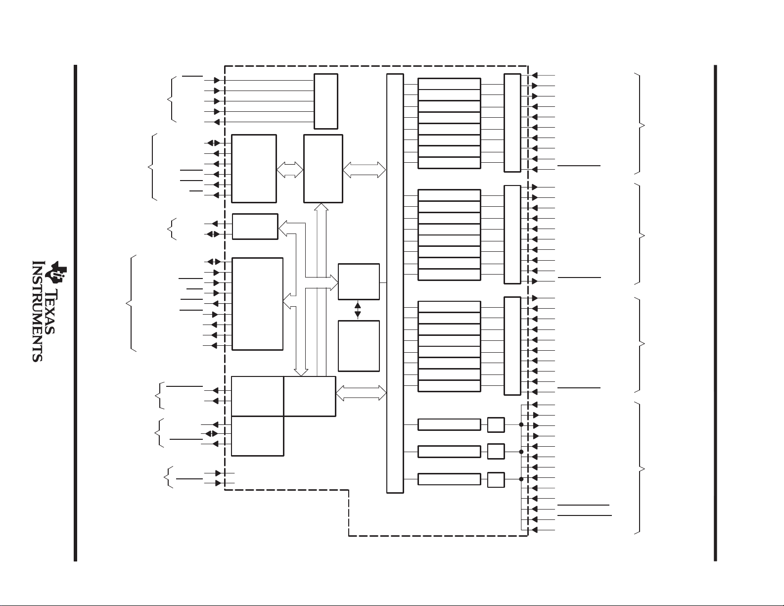
Figure 1. TNETX3270 Interface Block Diagram
PRODUCT PREVIEW
Page 6
TNETX3270
I/O
DESCRIPTION
ThunderSWITCH 24/3 ETHERNET SWITCH
WITH 24 10-MBIT/S PORTS AND 3 10-/100-MBIT/S PORTS
SPWS043B – NOVEMBER 1997 – REVISED APRIL 1999
Terminal Functions
10-Mbit/s MAC multiplexed interface (ports 00–23) is multiplexed into three groups (TH0, TH1, and
222
2
23
223
3
24
224
5
25
232
13
32
213
233
15
231
230
228
227
11
10
9
7
†
INTERNAL
RESISTOR
I Pullup
I Pulldown
I Pulldown
I Pulldown
O None
I Pullup
‡
Interface clock. Eight ports are supported on each interface and use this common 20-MHz
clock.
Interface collision sense. Assertion of THxCOL† during half-duplex operation indicates
network collision on the current port. Additionally, during full-duplex operation, transmission
of new frames does not start if this terminal is asserted.
Interface carrier sense. THxCRS† indicates a frame carrier signal is being received on a
current port.
Interface link presence. THxLINK† indicates the presence of the connection on a port.
– Low = no link
– High = link good
Interface renegotiate. A 1-0-1 sequence output on THxRENEG causes flow control and
half/full duplex for a port to be renegotiated with its companion physical-layer (PHY) device.
These THxRENEG
Interface receive data. The receive data nibble from the current port is synchronous to
THxCLK. When the THxRXDV signal is 1, the receive data terminals contain valid information.
THxRXD0 is the least significant bit and THxRXD3 is the most significant bit. These signals
also are used to report the channel state to the MAC.
terminals connect to IFFORCEHD on TNETE2008.
TH2) of eight ports
TERMINAL
NAME NO.
TH0CLK
TH1CLK
TH2CLK
TH0COL
TH1COL
TH2COL
TH0CRS
TH1CRS
TH2CRS
TH0LINK
TH1LINK
TH2LINK
TH0RENEG
TH1RENEG
TH2RENEG
TH0RXD3
TH0RXD2
TH0RXD1
TH0RXD0
TH1RXD3
TH1RXD2
TH1RXD1
TH1RXD0
TH2RXD3
TH2RXD2
TH2RXD1
TH2RXD0
TH0TXEN
TH1TXEN
TH2TXEN
TH0SYNC
TH1SYNC
TH2SYNC
†
THx = TH0, TH1, and TH2
‡
Internal resistors are provided to pull signals to known values. System designers should determine if additional pullups or pulldowns are required
in their system.
30
29
28
27
219
240
O None Interface transmit enable. THxTXEN indicates valid transmit data on THxTXD.
21
221
1
22
I Pullup
Interface synchronize. THxSYNC is used to synchronize the port traffic between the
media-access controller (MAC) and PHY. When THxSYNC is a 1, the current MAC-to-PHY
path is the multiplexer interface TH0, and the PHY-to-MAC path is the multiplexer interface
TH2. THxSYNC is sampled by the MAC on the falling edge of THxCLK.
6
POST OFFICE BOX 655303 • DALLAS, TEXAS 75265
Page 7
I/O
DESCRIPTION
I/O
DESCRIPTION
TNETX3270
ThunderSWITCH 24/3 ETHERNET SWITCH
WITH 24 10-MBIT/S PORTS AND 3 10-/100-MBIT/S PORTS
SPWS043B – NOVEMBER 1997 – REVISED APRIL 1999
Terminal Functions (Continued)
10-Mbit/s MAC multiplexed interface (ports 00–23) is multiplexed into three groups (TH0, TH1, and
20
19
18
16
6
26
42
65
90
43
66
92
54
80
104
52
78
102
53
79
103
44
67
93
†
(continued)
INTERNAL
RESISTOR
Interface transmit data. The transmit data nibble for the current port is synchronous to
O None
I Pulldown
THxCLK. When THxTXEN is asserted, these signals carry data. THxTXD3–THxTXD0 are
used during renegotiation to convey flow-control and duplex configuration requests to the
PHY. THxTXD0 is the least significant bit and THxTXD3 is the most significant bit.
Interface receive data valid. When THxRXDV is a 1, it indicates that the THxRXD lines contain
valid data.
‡
INTERNAL
RESISTOR
Collision sense. Assertion of MxxCOL in half-duplex signal indicates a network collision
I Pulldown
I Pulldown Carrier sense. MxxCRS indicates a frame carrier signal is being received.
§
I/O
I/O
Pullup
I Pulldown
‡
Pullup
I Pullup Receive clock. Receive clock source from the attached PHY or PMI device.
on that port. In full-duplex operation, transmission of new frames does not start if this
terminal is asserted.
Speed selection (force 10 Mbit/s is active low)
– If pulled low by either the TNETX3270 or a PHY, the port operates at 10 Mbit/s.
– If not pulled low by either the TNETX3270 or a PHY , the internal pullup resistor holds
this signal high and the port operates at 100 Mbit/s. An external 4.7-kΩ pullup resistor
connected to V
Connection status. MxxLINK indicates the presence of a port connection.
– If MxxLINK = 0, there is no link.
– If MxxLINK = 1, the link is good.
Duplex selection (force half duplex is active low)
– If pulled low by either the TNETX3270 or the PHY, the port operates at half duplex.
– If not pulled low by either the TNETX3270 or the PHY , the internal pullup resistor holds
this signal high and the port operates at full duplex. An external 4.7-kΩ pullup resistor
connected to V
DD(3.3V)
DD(3.3V)
may be required, depending on the system layout.
may be required, depending on the system layout.
TH2) of eight ports
TERMINAL
NAME NO.
TH0TXD3
TH0TXD2
TH0TXD1
TH0TXD0
TH1TXD3
TH1TXD2
TH1TXD1
TH1TXD0
TH2TXD3
TH2TXD2
TH2TXD1
TH2TXD0
TH0RXDV
TH1RXDV
TH2RXDV
†
THx = TH0, TH1, and TH2
218
217
216
215
239
237
236
234
226
10-/100-Mbit/s MAC interface (ports 24–26)
TERMINAL
NAME NO.
M24COL
M25COL
M26COL
M24CRS
M25CRS
M26CRS
M24FORCE10
M25FORCE10
M26FORCE10
M24LINK
M25LINK
M26LINK
M24FORCEHD
M25FORCEHD
M26FORCEHD
M24RCLK
M25RCLK
M26RCLK
‡
xx = ports 24, 25, and 26
§
Not a true bidirectional terminal. It can only be actively pulled down (open drain).
POST OFFICE BOX 655303 • DALLAS, TEXAS 75265
7
Page 8

TNETX3270
I/O
DESCRIPTION
ThunderSWITCH 24/3 ETHERNET SWITCH
WITH 24 10-MBIT/S PORTS AND 3 10-/100-MBIT/S PORTS
SPWS043B – NOVEMBER 1997 – REVISED APRIL 1999
Terminal Functions (Continued)
10-/100-Mbit/s MAC interface (ports 24–26) (continued)
TERMINAL
NAME NO.
M24RXD3
M24RXD2
M24RXD1
M24RXD0
M25RXD3
M25RXD2
M25RXD1
M25RXD0
M26RXD3
M26RXD2
M26RXD1
M26RXD0
M24RXDV
M25RXDV
M26RXDV
M24RXER
M25RXER
M26RXER
M24TCLK
M25TCLK
M26TCLK
M24TXD3
M24TXD2
M24TXD1
M24TXD0
49
48
47
46
73
71
70
69
98
97
96
95
50
75
99
51
76
101
33
56
82
38
37
36
35
INTERNAL
RESISTOR
Receive data (nibble receive data from the attached PHY or PMI device). Data on these
I Pullup
I Pulldown
I Pulldown Receive error. MxxRXER indicates a coding error on received data.
I Pullup Transmit clock. Transmit clock source from the attached PHY or PMI device.
signals is synchronous to MxxRCLK. MxxRXD0 is the least significant bit and MxxRXD3
is the most significant bit.
Receive data valid. When high, MxxRXDV indicates valid data is present on the
MxxRXD3–MxxRXD0 lines.
†
M25TXD3
M25TXD2
M25TXD1
M25TXD0
M26TXD3
M26TXD2
M26TXD1
M26TXD0
M24TXEN
M25TXEN
M26TXEN
M24TXER
M25TXER
M26TXER
†
xx = ports 24, 25, and 26
61
60
O None
59
57
86
85
84
83
39
62
O None Transmit enable. MxxTXEN indicates valid transmit data on MxxTXD3–MxxTXD0.
87
41
63
O None
89
Transmit data (nibble transmit data). When MxxTXEN is asserted, these signals carry
transmit data. Data on these signals is synchronous to MxxTCLK. MxxTXD0 is the least
significant bit and MxxTXD3 is the most significant bit.
Transmit error . MxxTXER allows coding errors to be propagated across the MII. MxxTXER
is taken high when an under-run in the transmit FIFO for port xx occurs and causes fill data
to be transmitted (MxxTXER is low otherwise). MxxTXER is asserted at the end of an
under-running frame, enabling the device to force a coding error .
8
POST OFFICE BOX 655303 • DALLAS, TEXAS 75265
Page 9
I/O
DESCRIPTION
SDRAM interface
TERMINAL
NAME NO.
DA13
DA12
DA11
DA10
DA09
DA08
DA07
DA06
DA05
DA04
DA03
DA02
DA01
DA00
DCAS
DCLK
DD31
DD30
DD29
DD28
DD27
DD26
DD25
DD24
DD23
DD22
DD21
DD20
DD19
DD18
DD17
DD16
DD15
DD14
DD13
DD12
DD11
DD10
DD09
DD08
DD07
DD06
DD05
DD04
DD03
DD02
DD01
DD00
DRAS
DW
212
210
209
207
206
205
204
203
202
200
199
198
196
195
189 O None
193 O None
187
186
185
183
182
181
180
179
177
176
174
173
172
171
170
168
167
166
164
162
161
159
158
157
156
155
153
152
150
149
147
146
190 O None SDRAM row address strobe. DRAS, with DCAS and DW, supplies the SDRAM commands.
191 O None SDRAM write select. DW, with DRAS and DCAS, supplies the SDRAM commands.
O None
I/O Pullup
TNETX3270
ThunderSWITCH 24/3 ETHERNET SWITCH
WITH 24 10-MBIT/S PORTS AND 3 10-/100-MBIT/S PORTS
SPWS043B – NOVEMBER 1997 – REVISED APRIL 1999
Terminal Functions (Continued)
INTERNAL
RESISTOR
SDRAM address bus (time-multiplexed bank, row, and column address). The address bus
DA13–DA00 also provides the SDRAM mode register initialization value. DA13 is the most significant
bit and DA00 is the least significant bit.
SDRAM column address strobe. DCAS, in conjunction with DRAS and DW, determines the SDRAM
commands.
SDRAM clock (83.33-MHz clock to the SDRAMs). SDRAM commands, addresses, and data are
sampled by the SDRAM on the rising edge of this clock.
SDRAM data bus (bidirectional bus used to carry SDRAM data). DD31–DD00 also output status
information to indicate buffer operation type and port number . Internal pullup resistors are provided.
DD31 is the most significant bit and the DD00 is the least significant bit.
POST OFFICE BOX 655303 • DALLAS, TEXAS 75265
9
Page 10
TNETX3270
I/O
DESCRIPTION
ThunderSWITCH 24/3 ETHERNET SWITCH
WITH 24 10-MBIT/S PORTS AND 3 10-/100-MBIT/S PORTS
SPWS043B – NOVEMBER 1997 – REVISED APRIL 1999
Terminal Functions (Continued)
host DIO interface
TERMINAL
NAME NO.
SAD1
SAD0
SCS
SDMA
SDATA7
SDATA6
SDATA5
SDATA4
SDATA3
SDATA2
SDATA1
SDATA0
SINT
SRDY
SRNW
SRXRDY
STXRDY
143
142
138 I Pullup DIO chip select. When low, SCS indicates a DIO port access is valid.
123 I Pullup
136
135
133
131
130
129
127
126
140 O None
139 O Pullup
125 I Pullup
145 O None
144 O None
INTERNAL
RESISTOR
I Pullup DIO address bus. SAD1 and SAD0 select the internal host registers, when SDMA is high.
DIO DMA select. When low, SDMA modifies the behavior of the DIO interface to allow it to operate
with an external DMA controller. The SAD0 and SAD1 terminals are not used to select the internal
host register for the access. Instead, the DIO address to access is provided by the DMA address
register, and one of two host register addresses is selected according to DMAinc in the Syscontrol
register.
– If DMAinc = 1, accesses are the DIOdatainc register and DMAaddress increments after each
access.
– If DMAinc = 0, accesses are the DIOdata register, and DMAaddress does not increment after
each address.
I/O Pullup
DIO data interface bus (byte-wide bidirectional DIO port). SDATA7 is the most significant bit and
SDATA0 is the least significant bit.
DIO interrupt line (interrupt to the attached microprocessor). The interrupt originating event is
stored in the Int register.
DIO ready signal
– When low during reads, SRDY
– When low during writes, SRDY
high. SRDY
DIO read not write
– When high, read operation is selected.
– When low, write operation is selected.
Network management port, receive ready. When high, SRXRDY indicates that the network
management port’s RX buffers are empty and the network management port is able to receive
a frame.
Network management port, transmit ready. STXRDY indicates that at least one frame buffer is
available to be read by the management CPU.
– It outputs as a 1 if any of the end-of-frame (EOF) bits, start-of-frame (SOF) bits, or one of the
bits in NMTxcontrol is set to 1.
– Otherwise, it outputs 0.
is driven high for one clock cycle before placing the output in high impedance.
indicates to the host when data is valid to be read.
indicates when data has been received after SCS is taken
10
POST OFFICE BOX 655303 • DALLAS, TEXAS 75265
Page 11
I/O
DESCRIPTION
I/O
DESCRIPTION
I/O
DESCRIPTION
I/O
DESCRIPTION
Terminal Functions (Continued)
serial MII management PHY interface
TERMINAL
NAME NO.
MDCLK
MDIO
MRESET
121 O/High Z Pullup
120 I/O Pullup
119 O/High Z Pullup
EEPROM interface
TERMINAL
NAME NO.
ECLK
EDIO
117 O None EEPROM data clock.
116 I/O Pullup
INTERNAL
RESISTOR
INTERNAL
RESISTOR
EEPROM data I/O. An external pulldown resistor may be required for proper operation. Since this
terminal has an internal pullup, it can be left unconnected if no EEPROM is present. The EEPROM
is optional if a management CPU is present.
TNETX3270
ThunderSWITCH 24/3 ETHERNET SWITCH
WITH 24 10-MBIT/S PORTS AND 3 10-/100-MBIT/S PORTS
SPWS043B – NOVEMBER 1997 – REVISED APRIL 1999
Serial MII management data clock. MDCLK can be disabled (high impedance) through the
use of the SIO register.
Serial MII management data I/O. MDIO can be disabled, placed in high Z, through the SIO
register. An external 4.7-kΩ pullup resistor , conected to V
rise-time requirements.
Serial MII management reset. MRESET can be disabled (high impedance) through the use
of the SIO register. If connected to a PHY device, an external pullup resistor is
recommended.
DD(3.3V)
, is needed to meet the
LED interface
TERMINAL
NAME NO.
LEDCLK
LEDDATA
113 O None LED clock (serial shift clock for the LED status data)
114 O None
JTAG interface
TERMINAL
NAME NO.
TCLK
TDI
TDO
TRST
TMS
106 I Pullup
110 I Pullup
108 O None
111 I Pullup
107 I Pullup
INTERNAL
RESISTOR
LED data (serial LED status data). LEDDATA is active low . All LED information (port link, activity
status, software status, flow status, and fault status) is sent via this serial interface.
INTERNAL
RESISTOR
T est clock. TCLK is used to clock state information, test instructions, and test data into and out of the
device during operation of the test port.
Test data input. TDI is used to serially shift test data and test instructions into the device during
operation of the test port. An internal pullup resistor is provided on TDI to ensure JT AG compliance.
T est data output. TDO is used to serially shift test data and test instructions out of the device during
operation of the test port.
T est reset. TRST is used for asynchronous reset of the test-port controller . An internal pullup resistor
is provided to ensure JTAG compliance. If the test port is not used, an external pulldown resistor of
10 kΩ may be used to disable the test-port controller.
T est mode select. TMS is used to control the state of the test-port controller. An internal pullup resistor
is provided on TMS to ensure JTAG compliance.
POST OFFICE BOX 655303 • DALLAS, TEXAS 75265
11
Page 12
TNETX3270
I/O
DESCRIPTION
DESCRIPTION
ThunderSWITCH 24/3 ETHERNET SWITCH
WITH 24 10-MBIT/S PORTS AND 3 10-/100-MBIT/S PORTS
SPWS043B – NOVEMBER 1997 – REVISED APRIL 1999
Terminal Functions (Continued)
miscellaneous
TERMINAL
NAME NO.
OSCIN
RESET
112 I None Master system clock input (83.33-MHz input clock)
115 I None Reset. RESET is synchronous and, therefore, the system clock must be operational during reset.
power interface
NAME NO.
8, 14, 34, 40, 55, 68, 74, 81, 88, 94, 100,
GND
V
DD(3.3V)
V
DD(2.5V)
128, 134, 141, 148, 154, 160, 175, 188,
12, 72, 109, 122, 132, 163, 169, 192, 229 None
105, 118, 124, 137, 151, 165, 178,
INTERNAL
RESISTOR
TERMINAL
194, 201, 208, 214, 220, 235
4, 17, 31, 45, 58, 64, 77, 91,
184, 197, 211, 225, 238
INTERNAL
RESISTOR
None
None 2.5-V supply voltage. Power for the core.
Ground. GND is the 0-V reference for the device. All GND
terminals must be connected.
3.3-V supply voltage. Power for the input, output, and I/O
terminals.
summary of signal terminals by signal group function
PORT DESCRIPTION
LED 2 1 2
10-Mbit/s port 16 3 48
10-/100-Mbit/s port 19 3 57
DIO 17 1 17
EEPROM interface 2 1 2
DRAM interface 50 1 50
Miscellaneous 2 1 2
JTAG 5 1 5
Serial MII management 3 1 3
Total signals 186
Assigned terminals 186
V
DD(3.3V)
V
DD(2.5V)
GND 25
Total terminals 240
NUMBER OF
SIGNALS
SUMMARY
MULTIPLIER TOTAL
9
20
12
POST OFFICE BOX 655303 • DALLAS, TEXAS 75265
Page 13
DIO register groups
TNETX3270
ThunderSWITCH 24/3 ETHERNET SWITCH
WITH 24 10-MBIT/S PORTS AND 3 10-/100-MBIT/S PORTS
SPWS043B – NOVEMBER 1997 – REVISED APRIL 1999
Table 1. Internal Register and Statistics Memory Map
LOADABLE
REGISTERS
Port configuration Yes Yes 0x0000:0x002F
Spanning tree Yes Yes 0x0030:0x007F
Trunking Yes Yes 0x0080:0x0088
VLAN No Yes 0x0089:0x03FF
Port status No No 0x0400:0x043F
Address configuration No No 0x0440:0x08FF
Port statistics No No 0x0900:0xFFFF
USING 24C02
EEPROM?
LOADABLE
USING 24C08
EEPROM?
DIO
ADDRESS
RANGE
POST OFFICE BOX 655303 • DALLAS, TEXAS 75265
13
Page 14

TNETX3270
ThunderSWITCH 24/3 ETHERNET SWITCH
WITH 24 10-MBIT/S PORTS AND 3 10-/100-MBIT/S PORTS
SPWS043B – NOVEMBER 1997 – REVISED APRIL 1999
Table 2. Detailed DIO Register Map
BYTE 3 BYTE 2 BYTE 1 BYTE 0
Port1control Port0control 0x0000
Port3control Port2control 0x0004
Port5control Port4control 0x0008
Port7control Port6control 0x000C
Port9control Port8control 0x0010
Port11control Port10control 0x0014
Port13control Port12control 0x0018
Port15control Port14control 0x001C
Port17control Port16control 0x0020
Port19control Port18control 0x0024
Port21control Port20control 0x0028
Port23control Port22control 0x002C
Port25control Port24control 0x0030
Reserved Port26control 0x0034
Reserved Reserved 0x0038:0x003F
Reserved UnkVLANport Mirrorport Uplinkport 0x0040
Reserved Aging threshold 0x0044
Reserved 0x0048:0x004F
Nlearnports 0x0050
Txblockports 0x0054
Rxuniblockports 0x0058
Rxmultiblockports 0x005C
Unkuniports 0x0060
Unkmultiports 0x0064
Unksrcports 0x0068
UnkVLANintports 0x006C
Reserved 0x0070:0x007F
Trunkmap3 T runkmap2 Trunkmap1 Trunkmap0 0x0080
Trunkmap7 Trunkmap6 Trunkmap5 Trunkmap4 0x0084
Reserved Trunkports 0x0088
Reserved 0x008C:0x009F
Devcode Reserved SIO Revision 0x00A0
Reserved 0x00A4:0x00DF
RAMsize Reserved IOBcontrol 0x00E0
Reserved 0x00E4
Pausetime100 Pausetime10 0x00E8
Reserved 0x00EC
Reserved Flowthreshold 0x00F0
Reserved LEDcontrol 0x00F4
Syscontrol Statcontrol 0x00F8
DIO
ADDRESS
14
POST OFFICE BOX 655303 • DALLAS, TEXAS 75265
Page 15

TNETX3270
ThunderSWITCH 24/3 ETHERNET SWITCH
WITH 24 10-MBIT/S PORTS AND 3 10-/100-MBIT/S PORTS
SPWS043B – NOVEMBER 1997 – REVISED APRIL 1999
Table 2. Detailed DIO Register Map (Continued)
BYTE 3 BYTE 2 BYTE 1 BYTE 0
Reserved (for EEPROM CRC) 0x00FC
VLAN0ports 0x0100
VLAN1ports 0x0104
VLAN2ports 0x0108
VLAN3ports 0x010C
VLAN4ports 0x0110
VLAN5ports 0x0114
VLAN6ports 0x0118
VLAN7ports 0x011C
VLAN8ports 0x0120
VLAN9ports 0x0124
VLAN10ports 0x0128
VLAN11ports 0x012C
VLAN12ports 0x0130
VLAN13ports 0x0134
VLAN14ports 0x0138
VLAN15ports 0x013C
VLAN16ports 0x0140
VLAN17ports 0x0144
VLAN18ports 0x0148
VLAN19ports 0x014C
VLAN20ports 0x0150
VLAN21ports 0x0154
VLAN22ports 0x0158
VLAN23ports 0x015C
VLAN24ports 0x0160
VLAN25ports 0x0164
VLAN26ports 0x0168
VLAN27ports 0x016C
VLAN28ports 0x0170
VLAN29ports 0x0174
VLAN30ports 0x0178
VLAN31ports 0x017C
Reserved 0x0180:0x02FF
VLAN1QID VLAN0QID 0x0300
VLAN3QID VLAN2QID 0x0304
VLAN5QID VLAN4QID 0x0308
VLAN7QID VLAN6QID 0x030C
VLAN9QID VLAN8QID 0x0310
VLAN11QID VLAN10QID 0x0314
VLAN13QID VLAN12QID 0x0318
VLAN15QID VLAN14QID 0x031C
DIO
ADDRESS
POST OFFICE BOX 655303 • DALLAS, TEXAS 75265
15
Page 16

TNETX3270
ThunderSWITCH 24/3 ETHERNET SWITCH
WITH 24 10-MBIT/S PORTS AND 3 10-/100-MBIT/S PORTS
SPWS043B – NOVEMBER 1997 – REVISED APRIL 1999
Table 2. Detailed DIO Register Map (Continued)
BYTE 3 BYTE 2 BYTE 1 BYTE 0
VLAN17QID VLAN16QID 0x0320
VLAN19QID VLAN18QID 0x0324
VLAN21QID VLAN20QID 0x0328
VLAN23QID VLAN22QID 0x032C
VLAN25QID VLAN24QID 0x0330
VLAN27QID VLAN26QID 0x0334
VLAN29QID VLAN28QID 0x0338
VLAN31QID VLAN30QID 0x033C
Reserved 0x0340:0x037F
Port1Qtag Port0Qtag 0x0380
Port3Qtag Port2Qtag 0x0384
Port5Qtag Port4Qtag 0x0388
Port7Qtag Port6Qtag 0x038C
Port9Qtag Port8Qtag 0x0390
Port11Qtag Port10Qtag 0x0394
Port13Qtag Port12Qtag 0x0398
Port15Qtag Port14Qtag 0x039C
Port17Qtag Port16Qtag 0x03A0
Port19Qtag Port18Qtag 0x03A4
Port21Qtag Port20Qtag 0x03A8
Port23Qtag Port22Qtag 0x03AC
Port25Qtag Port24Qtag 0x03B0
Reserved Port26Qtag 0x03B4
Reserved 0x03B8:0x03FF
Port1status Port0status 0x0400
Port3status Port2status 0x0404
Port5status Port4status 0x0408
Port7status Port6status 0x040C
Port9status Port8status 0x0410
Port11status Port10status 0x0414
Port13status Port12status 0x0418
Port15status Port14status 0x041C
Port17status Port16status 0x0420
Port19status Port18status 0x0424
Port21status Port20status 0x0428
Port23status Port22status 0x042C
Port25status Port24status 0x0430
Reserved Port26status 0x0434
Reserved 0x0438:0x043F
DIO
ADDRESS
16
POST OFFICE BOX 655303 • DALLAS, TEXAS 75265
Page 17
TNETX3270
ThunderSWITCH 24/3 ETHERNET SWITCH
WITH 24 10-MBIT/S PORTS AND 3 10-/100-MBIT/S PORTS
SPWS043B – NOVEMBER 1997 – REVISED APRIL 1999
Table 2. Detailed DIO Register Map (Continued)
BYTE 3 BYTE 2 BYTE 1 BYTE 0
Findnode<23–16> Findnode<31–24> Findnode<39–32> Findnode<47–40> 0x0440
FindVLAN Findcontrol Findnode<7–0> Findnode<15–8> 0x0444
Findport 0x0448
Newnode<23–16> Newnode<31–24> Newnode<39–32> Newnode<47–40> 0x044C
Reserved Newnode<7–0> Newnode<15–8> 0x0450
NewVLAN Newport 0x0454
Addnode<23–16> Addnode<31–24> Addnode<39–32> Addnode<47–40> 0x0458
AddVLAN Adddelcontrol Addnode<7–0> Addnode<15–8> 0x045C
Addport 0x0460
Agednode<23–16> Agednode<31–24> Agednode<39–32> Agednode<47–40> 0x0464
AgedVLAN Agedport Agednode<7–0> Agednode<15–8> 0x0468
Delnode<23–16> Delnode<31–24> Delnode<39–32> Delnode<47–40> 0x046C
DelVLAN Delport Delnode<7–0> Delnode<15–8> 0x0470
Agingcounter Numnodes 0x0474
Reserved 0x0478:0x07FF
Reserved DMAaddress 0x0800
Reserved Int 0x0804
Reserved Intenable 0x0808
Systest Freestacklength 0x080C
RAMaddress 0x0810
Reserved RAMdata 0x0814
Reserved NMRxcontrol 0x0818
Reserved NMTxcontrol 0x081C
Reserved NMdata 0x0820
Reserved 0x0824:0x3FFF
TNETX3270 reset: reinitializes the TNETX3270 0x4000:0x5FFF
Reserved 0x6000:0x7FFF
Port and network management port statistics 0x8000:8DFF
Reserved 0x8E00:8FFF
TX pause, RX pause, and security-violation counters 0x9000:0x91BF
Reserved 0x91C0:0x9FFF
Unknown unicast destination addresses 0xA000
Unknown multicast destination addresses 0xA004
Unknown source address 0XA008
Reserved 0xA00C:0xFFFF
DIO
ADDRESS
POST OFFICE BOX 655303 • DALLAS, TEXAS 75265
17
Page 18
TNETX3270
ThunderSWITCH 24/3 ETHERNET SWITCH
WITH 24 10-MBIT/S PORTS AND 3 10-/100-MBIT/S PORTS
SPWS043B – NOVEMBER 1997 – REVISED APRIL 1999
interface description
DIO interface
The DIO interface is a general-purpose interface that can be used with a wide range of microprocessor or
computer systems. The interface supports external DMA controllers.
This interface can be used to configure the TNETX3270 using an optional attached CPU (or EEPROM), and
to access statistics registers. In addition, this allows access to an internal network management (NM) port that
can be transferred between the CPU and the TNETX3270 to support spanning tree, SNMP, and RMON. Either
the CPU can read and write packets directly under software control or an external DMA controller can be used
to improve performance.
When accessing the statistics values from the DIO port, it is necessary to perform four 1-byte DIO reads to obtain
the full 32-bit counter. Counters always should be read in ascending byte-address order (0, 1, 2, 3). To prevent
the counter being updated while reading the four bytes, the entire 32-bit counter value is transferred to a holding
register when byte 0 is read.
receiving/transmitting management frames
Frames originating within the host are written to the NM port via the NMRxcontrol and NMdata registers. Once
a frame has been fully written, it is then received by the switch and routed to the destination port(s).
Frames that were routed to this port from any of the switch ports are placed in a queue until the host is ready
to read them via the NMTxcontrol and NMdata registers. They then are effectively transmitted out of the switch.
SDMA
can be used to transmit or receive management frames (the SAD1–SAD0 pins are ignored when SDMA
is asserted) (see Table 3). When SDMA is asserted, the switch uses the value in the DMAaddress register
instead of the DIO address registers to access frame data (this also can be used to access the switch statistics).
STXRDY and SRXRDY, the interrupts, freebuffs, eof, sof, and iof mechanisms can be used, as desired, to
prevent unwanted stalls on the DIO bus during busy periods.
Table 3. DMA Interface Signals
SIGNAL DESCRIPTION
SDMA Automatically sets up DIO address using the DMAaddress register
STXRDY Indicates that at least one data frame buffer can be read by the management CPU
SRXRDY Indicates that the management CPU can write a frame of any size up to 1535 bytes
state of DIO signals during hardware reset
The CPU can perform a hardware reset by writing to an address in the range 0x4000–0x5FFF (writes to a DMA
address in this range have no effect on reset). This is equivalent to asserting the hardware RESET
hardware reset, the output and bidirectional DIO pins behave as shown in Table 4.
Table 4. DIO Interface During Hardware Reset
DIO INTERFACE
SIGNAL
SDATA7–SDATA0 High impedance. Resistively pulled up.
SRDY High impedance. Resistively pulled up.
SRXRDY Driven high
STXRDY Driven low
STATE DURING HARDWARE RESET
pin. During
18
POST OFFICE BOX 655303 • DALLAS, TEXAS 75265
Page 19

TNETX3270
ThunderSWITCH 24/3 ETHERNET SWITCH
WITH 24 10-MBIT/S PORTS AND 3 10-/100-MBIT/S PORTS
SPWS043B – NOVEMBER 1997 – REVISED APRIL 1999
network management port
Frames can be received or transmitted via the DIO interface using a built-in port, the network management (NM)
port.
Frames originating within the host are written to this port via the NMRxcontrol and NMdata registers. Once a
frame has been fully written, it is then received by the switch and routed to the destination port(s).
Frames that were routed to this port from any of the switch’s ports queue until the host is ready to read them
via the NMTxcontrol and NMdata registers. They are then effectively transmitted out of the switch.
IEEE Std 802.1Q VLAN headers on the NM port
Frames received from the host via the NM port are required to contain a valid IEEE Std 802.1Q header. Frames
that do not contain a valid header are incorrectly routed. They may be corrupted at the transmission port(s), as
the header-stripping process does not verify that the four bytes after the source address are actually a valid
header because they always are a valid header under all other circumstances.
When a frame is transmitted to the NM port, no header-stripping occurs, so the frame contains one, or possibly
two headers, depending on how the frame was originally received.
full-duplex NM port
The NM port can intermix reception and transmission as desired. The direction of the NMdata access (i.e., read
or write) determines whether a byte is removed from the transmit queue or added to the receive queue. The
DIO interface is half duplex since it can do only a read or write at one time.
NM bandwidth and priority
The NM port is capable of transferring a byte to or from NMdata once every five cycles, so the burst rate of this
port approximates eight bits per 60 ns (or ≈133 Mbit/s). This can be sustained between the DIO port and the
NM port’s dedicated transmit or receive buffers.
However, the NM port is prioritized lower than the other ports between its receive and transmit buf fers and the
external memory system so that at periods of high activity , the NM port does not cause frames to be dropped
on the other ports. STXRDY and SRXRDY, the interrupts and freebuffs, EOF , SOF, and interior-of-frame (IOF)
mechanisms can be used as desired to prevent unwanted stalls on the DIO bus during busy periods.
The burst rate is unaffected by traffic on other ports.
interrupt processing
There are two interrupts available on the NM port.
The interrupt process uses RXRDY and the nmrx interrupts to indicate when the receive FIFO is empty. This
indicates that the NM port is ready to accept a frame of any length (up to 1536 bytes).
If the host needs to download a sequence of frames, it can use the freebuffs field to indicate space availability .
POST OFFICE BOX 655303 • DALLAS, TEXAS 75265
19
Page 20

TNETX3270
ThunderSWITCH 24/3 ETHERNET SWITCH
WITH 24 10-MBIT/S PORTS AND 3 10-/100-MBIT/S PORTS
SPWS043B – NOVEMBER 1997 – REVISED APRIL 1999
frame format on the NM port
The frame format on the NM port differs slightly from a standard Ethernet frame format. The key differences are:
the frame always contains an IEEE Std 802.1Q header in the four bytes following the source address (see
Figure 2). The TPID (tag protocol identifier or ethertype) field, however , is used in the switch for other purposes,
so a frame transmitted out of the switch on the NM port does not have the IEEE Std 802.1Q TPID of 81–00
(ethertype constant) value in these two bytes.
The first TPID byte output contains:
D
The frame source port number in the least significant bits. This allows the frame source port number to be
carried within the frame, which is useful for processing BPDUs, for example.
D
A cyclic redundancy check (CRC) type indicator (crctype) in the most significant bit (bit 7).
• If crctype = 1, then the CRC word in the frame excludes the IEEE Std 802.1Q header.
• If crctype = 0, then the CRC word in the frame includes the IEEE Std 802.1Q header. This CRC word is
for a regular IEEE Std 802.1Q frame format with the value in the IEEE Std 802.1Q TPID of 81–00
(ethertype constant) in the TPID field. Because the internal frame format uses the TPID field for other
purposes in the manner being described, it is necessary to insert the IEEE Std 802.1Q TPID of 81–00
(ethertype constant) value into the TPID field if the frame needs to be restored to a normal
IEEE Std 802.1Q frame format, which passes a CRC check.
T o provide a CRC word, which includes the header , the NM port generates a new CRC word as the frame is
being read out. It simultaneously checks the existing CRC in the frame and, if an error is found, ensures that
the final byte of the newly generated CRC is corrupted to contain an error, too. The CRC word is deliberately
corrupted if the header parity protection (described in the following) indicates an error in the header. In either
case, the pfe bit also is set to 1 after the final byte of the frame has been read from NMdata.
If the frame was received on a port other than the NM port, then the crctype bit is set if an IEEE Std 802.1Q
tag header was inserted into the frame during ingress.
• If crctype = 1, a header was inserted.
• If crctype = 0, a header was not inserted (crctype also is 0 if the frame VLAN ID was 0x000 and was
replaced by the port VLANID (PVID) from the PortxQtag register).
In an IEEE Std 802.1D-compliant application, the header simply can be removed from the frame to produce
a headerless frame with a correct CRC word.
• All other bits in the byte are reserved and are 0.
The second TPID byte output contains:
D
Odd-parity protection bits for the other three bytes in the tag header
D
Bit 5 protects the first byte of the TPID field (i.e., the one containing crctype and source port number).
D
Bit 6 protects the first byte of the VLAN ID field.
D
Bit 7 protects the second byte of the VLAN ID field.
D
All other bits in the byte are reserved and are 0.
20
POST OFFICE BOX 655303 • DALLAS, TEXAS 75265
Page 21

frame format on the NM port (continued)
TPID (Tag Protocol Identifier) TCI (Tag Control Information)
10000 0001 0000000
6543 21076 543 21 0 7 6 5 4 32107654321 0
7
TNETX3270
ThunderSWITCH 24/3 ETHERNET SWITCH
WITH 24 10-MBIT/S PORTS AND 3 10-/100-MBIT/S PORTS
SPWS043B – NOVEMBER 1997 – REVISED APRIL 1999
Priority cfi VLAN ID
Destination
Address
6 Bytes
CRC
Type
75436
Source
Address
6 Bytes
Reserved
802.1Q header
TPID TCI
2 Bytes
Byte 1 Byte 2
2 Bytes 46–1517 Bytes2 Bytes
Source
Port
2107 5436210
Length/Type
Odd Parity Bits
2nd
TCI
Byte
1st
TCI
Byte
Data
1st
TPID
Byte
Reserved
FCS
(CRC-32)
4 Bytes
Figure 2. NM Frame Format
Any device reading frames out of the NM port must expect frames to be in the format shown in Figure 2.
Frames received into the switch on the NM port also must conform to this format, with the following caveats:
D
crc = 0 in NMRxcontrol
When the host provides a frame containing valid CRC it also must provide in the TPID field valid header
parity protection and indicate via the crctype bit which type of CRC the frame contains [i.e., including the
header (crctype = 0), or excluding the header (crctype = 1)]. If crctype indicates that the header is included,
as for NM port transmissions, this pretends that IEEE Std 802.1Q TPID of 81–00 (ethertype constant) is
present in the TPID field. If a CRC error or parity error is detected, the frame is discarded.
When
crctype indicates that the header is included, the NM port regenerates CRC to exclude the header
during the reception process (this converts the frame into the required internal frame format).
D
crc = 1 in NMRxcontrol
If the switch is asked to generate a CRC word for the frame, the values in the TPID field are ignored by the
NM port. The switch inserts header parity protection. It replaces the final four bytes of the frame with the
calculated CRC (the values in the final four bytes provided are don’t care).
In either case, the NM port inserts its own port number into the source port field in the least significant bits of
the first TPID byte, sets the crctype bit to 0, and also sets the reserved bits to 0.
Frames received from the host via the NM port must contain a valid IEEE Std 802.1Q VLAN ID in the third and
fourth bytes, following the source address (the NM port does not have a PortxQtag register for inserting a VLAN
tag if none is provided and does not have an
rxacc bit). Frames that do not contain a VLAN tag are incorrectly
routed. They also can be corrupted at the transmission port(s). The header-stripping process does not verify
that the two bytes after the source address are a valid IEEE Std 802.1Q TPID because there is a valid header
under all other circumstances.
POST OFFICE BOX 655303 • DALLAS, TEXAS 75265
21
Page 22

TNETX3270
ThunderSWITCH 24/3 ETHERNET SWITCH
WITH 24 10-MBIT/S PORTS AND 3 10-/100-MBIT/S PORTS
SPWS043B – NOVEMBER 1997 – REVISED APRIL 1999
frame format on the NM port (continued)
When a frame is transmitted on the NM port, no header stripping occurs (again because the NM port does not
have a PortxQtag register or
more, depending on how the frame was received).
In either case, the NM port inserts its own port number into the source port field in the least significant bits of
the first TPID byte and sets the reserved bits to 0. Frames received from the host via the NM port are required
to contain a valid IEEE Std 802.1Q VLAN ID (VID) in the third and fourth bytes following the source address.
(The NM port does not have a default VLAN ID register for inserting a VLAN tag if none is provided. It cannot
also be configured as an access port.) Frames that do not contain a valid tag are incorrectly routed. They also
can be corrupted at the transmission port(s), as the tag-stripping process does not verify that the four bytes after
the source address are a valid tag because they are valid tags under all other circumstances.
When a frame is transmitted on (read from) the NM port, no tag stripping occurs (because the NM port does
not have the default VLAN ID register or access configuration control), so the frame read by the host software
can contain one or more header tags, depending on how the frame was received.
MII serial management interface (PHY management)
This interface gives the user an easy way to implement a software-controlled bit serial MII.
MII devices that implement the management interface, consisting of MDIO and MDCLK, can be accessed in
this way through the SIO register. The direction of MDIO is controlled by the SIO register. In addition, a third
signal, MRESET
, is provided to allow hardware reset of PHYs that support it.
txacc bit), so the frame read by the host software contains one header (or possibly
All three signals have internal pullup resistors, since they all can be placed into high impedance via the MDIOEN
bit of the SIO register, to allow another bus master.
The interface does not implement timing or data structure. The timing and frame format must be ensured by
the management software setting the bits within the SIO register in an appropriate manner. Refer to IEEE Std
802.2u and MII data sheets for the appropriate protocol requirements.
10-Mbit/s and 10-/100-Mbit/s MAC interface
receive control
Data received from the PHYs is interpreted and assembled into the TNETX3270 buffer memory . Interpretation
involves detection and removal of the preamble, extraction of the address and frame length, extraction of the
IEEE Std 802.1Q header (if present), and data handling and CRC. A jabber-detection timer also is included to
detect frames that exceed maximum length being received on the network.
giant (long) frames
The maxlen bit within each port’s Portxcontrol register controls the maximum received frame size on that port.
D
If maxlen = 0, the maximum received frame length Is 1535 bytes if no VLAN header is inserted, or 1531 bytes
if a VLAN header is inserted. (When stored within the switch, a frame never can be longer than 1535 bytes.)
D
If maxlen = 1, the maximum received frame length is 1518 bytes, as specified by the IEEE Std 802.3. This
is the maximum length on the wire. If a VLAN header is inserted into a 1518-byte frame within the MAC,
the frame is stored as a 1522-byte frame within the switch.
All received frames longer than the maximum size are discarded by the switch.
The long option bit in StatControl indicates how the statistics for long frames should be recorded.
short frames
All received frames shorter than 64 bytes are discarded upon reception and are not stored in memory or
transmitted.
22
POST OFFICE BOX 655303 • DALLAS, TEXAS 75265
Page 23

TNETX3270
ThunderSWITCH 24/3 ETHERNET SWITCH
WITH 24 10-MBIT/S PORTS AND 3 10-/100-MBIT/S PORTS
SPWS043B – NOVEMBER 1997 – REVISED APRIL 1999
receive filtering of frames
Received frames that contain an error (e.g., CRC, alignment, jabber, etc.) are discarded before transmission
and the relevant statistics counter is updated.
data transmission
The MAC takes data from the TNETX3270 internal buffer memory and passes it to the PHY. The data also is
synchronized to the transmit clock rate.
A CRC block verifies that the outgoing frame has not been corrupted within the switch by verifying that it still
has a valid CRC as the frame is being transmitted. If a CRC error is detected, it is counted in the transmit data
errors counter.
transmit control
The frame control block handles the output of data to the PHYs. Several error states are handled. If a collision
is detected, the state machine jams the output. If the collision was late (after the first 64-byte buffer has been
transmitted), the frame is lost. If it is an early collision, the controller backs off before retrying. While operating
in full duplex, both carrier-sense (CRS) mode and collision-sensing modes are disabled (the switch does not
start transmitting a new frame if collision is active in full-duplex mode).
Internally, frame data only is removed from buffer memory once it has been successfully transmitted without
collision (for the half-duplex ports). Transmission recovery also is handled in this state machine. If a collision
is detected, frame recovery and retransmission are initiated.
adaptive performance optimization (APO) (transmit pacing)
Each Ethernet MAC incorporates APO logic. This can be enabled on an individual port basis. When enabled,
the MAC uses transmission pacing to enhance performance (when connected on networks using other transmit
pacing-capable MACs). Adaptive performance pacing introduces delays into the normal transmission of
frames, delaying transmission attempts between stations, reducing the probability of collisions occurring during
heavy traffic (as indicated by frame deferrals and collisions), thereby, increasing the chance of successful
transmission.
When a frame is deferred, suffers a single collision, multiple collisions, or excessive collisions, the pacing
counter is loaded with an initial value of 31. When a frame is transmitted successfully (without a deferral, single
collision, multiple collision, or excessive collision), the pacing counter is decremented by 1, down to 0.
With pacing enabled, a new frame is permitted to immediately [after one inter-packet gap (IPG)] attempt
transmission only if the pacing counter is 0. If the pacing counter is not 0, the frame is delayed by the pacing
delay (a delay of approximately four interframe gap delays).
NOTE:
APO affects only the IPG preceding the first attempt at transmitting a frame. It does not affect the
backoff algorithm for retransmitted frames. APO should be used only with other endstations that
also support APO.
interframe gap enforcement
The measurement reference for the interpacket gap of 96-bit times is changed, depending on frame traffic
conditions. If a frame is transmitted successfully (without collision), 96-bit times is measured from MxxTXEN.
If the frame suffered a collision, 96-bit times is measured from MxxCRS.
backoff
The device implements the IEEE Std 802.3 binary exponential backoff algorithm.
POST OFFICE BOX 655303 • DALLAS, TEXAS 75265
23
Page 24

TNETX3270
ThunderSWITCH 24/3 ETHERNET SWITCH
WITH 24 10-MBIT/S PORTS AND 3 10-/100-MBIT/S PORTS
SPWS043B – NOVEMBER 1997 – REVISED APRIL 1999
receive versus transmit priority
The queue manager prioritizes receive and transmit traffic as follows:
D
Highest priority is given to frames that currently are being transmitted. This ensures that transmitting frames
do not underrun.
D
Next priority is given to frames that are received if the free-buffer stack is not empty. This ensures that
received frames are not dropped unless it is impossible to receive them.
D
Lowest priority is given to frames that are queued for transmission but have not yet started to transmit.
These frames are promoted to the highest priority only when there is spare capacity on the memory bus.
D
The NM port receives the lowest priority to prevent frame loss during busy periods.
The memory bus has enough bandwidth to support the two highest priorities. The untransmitted frame queues
grow when frames received on different ports require transmission on the same port(s) and when frames are
repeatedly received on ports that are at a higher speed than the ports on which they are transmitted. This is likely
to be exacerbated by the reception of multicast frames, which typically require transmission on several ports.
When the backlog grows to such an extent that the free buffer stack is nearly empty, flow control is initiated (if
it has been enabled) to limit further frame reception.
uplink pretagging
TNETX3270 can be incorporated into a switch where routing decisions can be made at a higher level. To
facilitate this, two forms of tags are provided on ports 24–26:
D
Source-port pretag on transmission
D
Port-routing-code pretag on reception
source-port pretag on transmission
Ports 24–26 provide the frame’s source-port-number pretag one cycle before MxxTXEN goes high (this tag is
ignored by an externally connected PHY). The 5-bit tag appears as an encoding on terminals MxxTXER and
MxxTXD3 to MxxTXD0 (most significant bit to least significant bit). This is shown in Figure 3 and Table 5.
MxxTCLK
MxxTXER
MxxTXD3–MxxTXD0
MxxTXEN
Figure 3. Source-Port Pretag
Transmit ErrorTag MSB
Preamble and FrameTag LS 4 Bits
24
POST OFFICE BOX 655303 • DALLAS, TEXAS 75265
Page 25

TNETX3270
ThunderSWITCH 24/3 ETHERNET SWITCH
WITH 24 10-MBIT/S PORTS AND 3 10-/100-MBIT/S PORTS
SPWS043B – NOVEMBER 1997 – REVISED APRIL 1999
Table 5. Source-Port Pretag Encoding
MxxTXER
0 0000 Port 00
0 0001 Port 01
0 0010 Port 02
0 0011 Port 03
0 0100 Port 04
0 0101 Port 05
0 0110 Port 06
0 0111 Port 07
0 1000 Port 08
0 1001 Port 09
0 1010 Port 10
0 1011 Port 11
0 1100 Port 12
0 1101 Port 13
0 1110 Port 14
0 1111 Port 15
1 0000 Port 16
1 0001 Port 17
1 0010 Port 18
1 0011 Port 19
1 0100 Port 20
1 0101 Port 21
1 0110 Port 22
1 0111 Port 23
1 1000 Port 24
1 1001 Port 25
1 1010 Port 26
1 1011 Port 27 (NM port)
1 11xx Reserved
MxxTXD3–
MxxTXD0
SOURCE PORT
POST OFFICE BOX 655303 • DALLAS, TEXAS 75265
25
Page 26

TNETX3270
ThunderSWITCH 24/3 ETHERNET SWITCH
WITH 24 10-MBIT/S PORTS AND 3 10-/100-MBIT/S PORTS
SPWS043B – NOVEMBER 1997 – REVISED APRIL 1999
port-routing-code pretag on reception
If the pretag bit is set to 1 in the appropriate Portxcontrol register, during the seven MxxRCLK cycles prior to
MxxRXDV going high, the port expects to receive a seven-nibble pretag on MxxRXD3–MxxRXD0 (see
Figure 4).
MxxRCLK
MxxRXD3–
MxxRXD0
MxxRXDV
Tag 5 Tag 4 Tag 3 Tag 2 Tag 1 T ag 0
Preamble and FrameTag 6
Figure 4. Port-Routing-Code Pretag
Each of the 28 bits contained within these nibbles represents a destination port for the frame. If a bit is 1, the
frame is queued to that port. If the port is disabled or its link is inactive, the frame subsequently is drained from
the port’s queue, which again returns to zero length.
The port assignments for these tag bits are shown in Table 6.
Table 6. Received Pretag Port Assignments
TAG MxxRXD3 MxxRXD2 MxxRXD1 MxxRXD0
6 Port 27 (NM) Port 26 Port 25 Port 24
5 Port 23 Port 22 Port 21 Port 20
4 Port 19 Port 18 Port 17 Port 16
3 Port 15 Port 14 Port 13 Port 12
2 Port 11 Port 10 Port 09 Port 08
1 Port 07 Port 06 Port 05 Port 04
0 Port 08 Port 02 Port 01 Port 00
The 28 bits are examined during the reception process to see if just one destination bit is set. If this is the case,
the frame is received and handled like a unicast frame (such frames can be cut through). If more than one bit
is set, the frame is handled as an in-order-broadcast (and cannot be cut through). The frame is routed to all the
port(s) specified regardless of whether the destination address is unicast or multicast (i.e., the destination
address is not examined).
If all 28 tag bits are 0, the frame is discarded. If the frame has not been discarded in the MAC (for some reason),
the portx-filtered RX-frames statistic is incremented.
The tag bits are not examined to see if the source port is specified as a destination port, so it is possible, for
example, for port 25 to send a frame to itself by setting bit 1 in tag 6.
The IALE sees and processes pretagged frames exactly as nonpretagged frames (it does not know that a frame
has been pretagged). However, the final port-routing code generated by the IALE is ignored (the information
in the pretag determines the destination ports). Normal IALE behavior occurs in terms of address learning and
interrupt generation and statistics updates with one exception – the portx-filtered RX-frames statistic is
incremented if the pretag contained all 0s. (Whether or not the IALE generates its own (ignored) port-routing
code of all 0s has no effect on this statistic if the frame is a pretagged frame.)
Since the IALE’s routing decision is ignored on pretagged frames, the Txblockports, Rxuniblockports, and
Rxmultiblockports registers have no effect on frame reception or transmission.
26
POST OFFICE BOX 655303 • DALLAS, TEXAS 75265
Page 27

TNETX3270
ThunderSWITCH 24/3 ETHERNET SWITCH
WITH 24 10-MBIT/S PORTS AND 3 10-/100-MBIT/S PORTS
SPWS043B – NOVEMBER 1997 – REVISED APRIL 1999
EEPROM interface
The EEPROM interface is provided so the system-level manufacturer can produce a CPU-less, preconfigured
system to their customers. Customers also may want to change or reconfigure their system and retain their
preferences between system power downs. The device cannot be used without either an EEPROM or CPU
connected to it (see Figure 5).
The EEPROM contains configuration and initialization information that are accessed infrequently, typically at
power up and after a reset. The organization of the EEPROM data is in accordance with the DIO address map.
EEPROM downloads can be initiated in one of two ways:
D
At the end of hard reset (rising edge on RESET, or completion of a DIO write to DIOaddrhi register that
changes the value of the three most significant bits from 010 to another value).
D
Writing a 1 to load in Syscontrol register. This bit is cleared automatically when the download completes.
It cannot be set during the download by the EEPROM data, thereby preventing a download loop.
During the download, no DIO writes are permitted. If a DIO write is attempted, SRDY
is held high until the
download has completed.
The EEPROM size is detected automatically according to the address assigned to the EEPROM:
D
2048 bits organized as a 256 × 8 EEPROM should have its A0, A1, and A2 pins tied low.
D
8192 bits organized as a 1024 × 8 EEPROM should have its A0 and A1 pins tied low and A2 pin tied high.
EDIO
TNETX3270
ECLK
SCL SDA
24C0x
Flash EEPROM
A0 A1 A2
GND
24C02 = GND
24C08 = V
DD
Figure 5. EEPROM Interface Connections
After the initial start condition, a slave address containing a device address of 000 is output on EDIO, and then
EDIO is observed for an acknowledge from the EEPROM. If an acknowledge is received, operation continues
for the 24C02 EEPROM. If none is received, a stop condition is generated, followed by another start condition
and slave address, this time containing a device address of 100. If this receives no acknowledge, no EEPROM
is present, and device operation continues, using the current register settings (i.e., those following a hardware
reset, or those previously entered by software).
When this device is driving EDIO, it drives out only a strong logic 0. When a logic 1 is intended to be driven out,
the pin must be resistively pulled high. An on-chip 50-µA current-source pullup device is provided on this pin.
The system designer must decide if this is sufficient to achieve a logic 1 level in a timely manner or if an external
supplementary resistor is required.
POST OFFICE BOX 655303 • DALLAS, TEXAS 75265
27
Page 28

TNETX3270
ThunderSWITCH 24/3 ETHERNET SWITCH
WITH 24 10-MBIT/S PORTS AND 3 10-/100-MBIT/S PORTS
SPWS043B – NOVEMBER 1997 – REVISED APRIL 1999
EEPROM interface (continued)
Multiple bus masters are not supported on the EEPROM interface because the ECLK pin always is driven by
the device with a strong 0/strong 1 (i.e., not a strong 1/resistively pulled-up 1).
An Ethernet CRC check is used to ensure the EEPROM data is valid. The 4-byte CRC should be placed within
the EEPROM in four data bytes immediately following the last byte to be loaded (equivalent to locations
0x00FC–0x00FF, just above Syscontrol). As each byte is loaded from the EEPROM, the bits within that byte
are entered into the CRC checker bit-wise, most significant bit first.
A valid CRC always must be provided by the EEPROM. The EEPROM data for the most significant bit of
Syscontrol is withheld until the CRC computed by the device has been checked against the one read from the
EEPROM. If the CRC is invalid:
D
The reset bit is set to 1 in Syscontrol, load and initd are both 0, and the TNETX3270 does not begin
operation.
D
The fault LED is illuminated and remains in that state until the TNETX3270 is hardware reset or until load
in Syscontrol is set to 1.
interaction of EEPROM load with the SIO register
The EDIO pin is shared with the SIO register edata bit. The edata and etxen bits must not both be set to 1 when
the load bit is set or the EDIO pin is held at resistive 1 and the EEPROM load fails.
The value of the eclk bit in SIO is don’t care when load is set, but to ensure the EEPROM does not see a glitch
on its clock signal, the load bit should not be set until the minimum clock high or low time required by the
EEPROM on its clock signal has expired since the eclk bit was last changed.
The SIO register is not loaded during the EEPROM download.
summary of EEPROM load outcomes
Table 7 summarizes the various states of register bits and the fault LED for each possible outcome, following
an EEPROM load attempt.
Table 7. Summary of EEPROM Load Outcomes
OUTCOME STOP LOAD INITD†FAULT LED ECLK
Successful load 0 0 1 0
No EEPROM present 0 0 0 0
CRC error detected 1 0 0 1 Not locked
†
Assuming the start bit was set to 1 by the EEPROM load
‡
Assuming the fault bit in LEDControl = 0 and no memory system parity error is detected
‡
‡
Not locked
Locked
compatibility with future device revisions
All EEPROM locations that correspond to reserved addresses in the memory map, register bits that are read
only , and register bits that are marked as reserved should be set to 0 to ensure compatibility with future versions
of the device. Failure to do so may result in the unintentional activation of features in future devices. All such
bits are included in the CRC calculation.
28
POST OFFICE BOX 655303 • DALLAS, TEXAS 75265
Page 29

TNETX3270
ThunderSWITCH 24/3 ETHERNET SWITCH
WITH 24 10-MBIT/S PORTS AND 3 10-/100-MBIT/S PORTS
SPWS043B – NOVEMBER 1997 – REVISED APRIL 1999
JTAG interface
The TNETX3270 is fully IEEE Std 1 149.1 compliant. It also includes on-chip pullup resistors on the five JTAG
terminals to eliminate the need for external ones. All JTAG inputs and outputs are 3.3-V tolerant.
The following instructions are supported:
D
EXTEST, BYPASS, and SAMPLE/PRELOAD
D
HIGHZ and IDCODE
D
Private (various private instructions are used by TI for test purposes)
The opcodes for the various instructions (6-bit instruction register) are shown in Table 8.
Table 8. JTAG Instruction Opcodes
INSTRUCTION
TYPE
Mandatory EXTEST 000000
Mandatory SAMPLE/PRELOAD 000001
Optional IDCODE 000100
Optional HIGHZ 000101
Optional RACBIST 000110
Private TI testing Others
Mandatory BYP ASS 111111
INSTRUCTION
NAME
JTAG
OPCODE
HIGHZ instruction
When selected, the HIGHZ instruction causes all outputs and bidirectional pins to become high impedance. All
pullup and pulldown resistors are disabled.
LED interface
This interface allows a visual status for each port to be displayed. In addition, the state of the internal flow control
and fault functions are displayed along with 12 software-controllable LEDs.
Each port has a single LED, which can convey three states (see Table 9).
Table 9. LED States
STATE DISPLAY
No link Off
Link, but no activity On
Activity (bits moving) Flashing at 8 Hz
The interface is intended for use with external octal shift registers clocked with LEDCLK. Every 16th of a second,
all the status bits are shifted out via LEDDATA
.
The status bits are shifted out in one of two possible orders, as determined by slast in LEDControl, to ensure
that systems that do not require all the LED status can be implemented with the minimum number of octal shift
registers (see Table 10).
D
If slast = 0, the software-controlled status bits are shifted out before the port status bits.
D
If slast = 1, the software-controlled status bits are shifted out after the port status bits.
The fault status bit is shifted out last, enabling a minimal system that displays only the fault status to be
implemented without any shift registers.
POST OFFICE BOX 655303 • DALLAS, TEXAS 75265
29
Page 30

TNETX3270
NAME
FUNCTION
ThunderSWITCH 24/3 ETHERNET SWITCH
WITH 24 10-MBIT/S PORTS AND 3 10-/100-MBIT/S PORTS
SPWS043B – NOVEMBER 1997 – REVISED APRIL 1999
Table 10. LED Status Bit Definitions and Shift Order
ORDER
slast = 0 slast = 1
1–7 1–7 0 Zero. Dummy data for first seven of 48 LEDCLK cycles.
Software LEDs 0–11. These allow additional software-controlled status to be displayed. These
8–19 35–46 SW0–SW11
20–46 8–34 P00–P26
47 47 FLOW
48 48 FAULT
12 LEDs reflect the values of bits 0–11 of the swled field in LEDControl
interface samples them. If this occurs between writes to the most significant and least significant
bytes of LEDControl, these values appear on the LEDs, separated by 1/16th of a second.
Port status LEDs 00–26. These 27 LEDs indicate the status of ports 00–26, in this order (port 00
is output first). Note that port 27 (management port) does not have an LED. The transmit multicast
content of these bits can be controlled by the txais bit in LEDControl. Note that IEEE Std 802.3X
pause frames never appear on the LEDs as port activity. The port’ s LED toggles each 1/16th of a
second if there was any frame traffic (other than pause frames) on the port during the previous
1/16th of a second.
Flow control. LED is on when the internal flow control is enabled and active. Active means that flow
control is asserted during the previous 1/16th of a second.
Fault. LED indicates:
– the EEPROM CRC is invalid.
– an external DRAM parity error has occurred.
– the fitled in LEDControl has been set.
The CRC and parity error indications are cleared by hardware reset (terminal or DIO). The CRC
error indication also is cleared by setting load to 1. The parity error indication also is cleared by
setting start to 1.
at the moment that the LED
lamp test
When the device is in the hardware reset state, LEDDA TA is driven high and LEDCLK runs continuously. This
causes all LEDs to be illuminated and serves as a lamp test function.
multi-LED display
The LED interface is intended to provide the lowest-cost display with a single multifunction LED per port. In
systems requiring a full-feature display (more than levels of activity) using multiple LEDs per port, this can be
achieved by driving the LEDs directly from the PHY signals.
hardware configurations
10-Mbit/s MAC interfaces (ports 00–23)
Each group of eight 10-Mbit/s ports (ports 00 to 07, 08 to 15, and 16 to 23) interfaces directly with a TI
TNETE2008, which contains eight 10-Mbit/s PHYs. This interface is time multiplexed between the eight ports,
with receive and transmit data being transferred over nibble-wide buses. Any given port needs only to transfer
data at 2.5 MHz (i.e., 2.5 MHz × 4 bits = 10 Mbit/s), but because TNETE2008 contains eight PHYs, the frequency
of nibble transfers is 20 MHz (i.e., 2.5 MHz × 8 ports). The remaining control and status signals also are
transferred at this rate.
Table 11 shows how the terminals of a TNETE2008 device are connected to each 10-Mbit/s interface on the
TNETX3270.
30
POST OFFICE BOX 655303 • DALLAS, TEXAS 75265
Page 31

TNETX3270
ThunderSWITCH 24/3 ETHERNET SWITCH
WITH 24 10-MBIT/S PORTS AND 3 10-/100-MBIT/S PORTS
SPWS043B – NOVEMBER 1997 – REVISED APRIL 1999
Table 11. 10-Mbit/s Interface Connections
TNETX3270
TERMINAL
THxCLK ← IFCLK
THxSYNC ← IFSYNC
THxCOL ← IFCOL
THxCRS ← IFCRS
THxLINK ← IFLINK
THxRXD3 ← IFRXD3
THxRXD2 ← IFRXD2
THxRXD1 ← IFRXD1
THxRXD0 ← IFRXD0
THxRXDV ← IFRXDV
THxTXD3 → IFTXD3
THxTXD2 → IFTXD2
THxTXD1 → IFTXD1
THxTXD0 → IFTXD0
THxTXEN → IFTXEN
THxRENEG → IFFORCEHD
Where x = 0, 1, or 2
TNETE2008
TERMINAL
The time multiplexing of this interface is shown in Figure 6. The interface runs synchronous to the
PHY -generated 20-MHz clock IFCLK. The MAC-to-PHY information for the first port in each group of eight (i.e.,
port 00, port 08, or port 16) is presented on the interface when the THxSYNC terminal is high. The next clock
cycle that the interface carries is the information for the second port. This process continues for all eight ports,
each using the interface for one cycle. When all ports have been processed in this manner, the sequence
resumes with the first port and again when the THxSYNC signal is asserted.
T o improve latency-related issues, the PHY -to-MAC data are skewed by two slots, allowing the MAC to respond
to the input signals from the PHY in the same 400-ns cycle, rather than waiting for the next 400-ns cycle (which
would be the case if the signals were not skewed).
POST OFFICE BOX 655303 • DALLAS, TEXAS 75265
31
Page 32

TNETX3270
ThunderSWITCH 24/3 ETHERNET SWITCH
WITH 24 10-MBIT/S PORTS AND 3 10-/100-MBIT/S PORTS
SPWS043B – NOVEMBER 1997 – REVISED APRIL 1999
PORT
CLK
SYNC
TXD3-
TXD0
TXEN
FORCEHD
COL
CRS
LINK
RXD3-
RXD0
RXDV
0
M00TXD M01TXD M02TXD M03TXD M04TXD M05TXD M06TXD M07TXD M00TXD M01TXD
M00TXEN
M00FHD
M02COL
M02CRS
M02LINK
M02RXD
M02RXDV
1
M01TXEN M02TXEN M03TXEN M04TXEN M05TXEN M06TXEN M07TXEN M00TXEN M01TXEN
M01FHD
M03COL M04COL M05COL M06COL M07COL M00COL M01COL M02COL M03COL
M03CRS
M03LINK
M03RXD
M03RXDV
23456701
M02FHD M03FHD M04FHD M05FHD M06FHD M07FHD M00FHD M01FHD
M04CRS
M04LINK
M04RXD
M04RXDV
M05CRS
M05LINK
M05RXD
M05RXDV
M06CRS
M06LINK
M06RXD
M06RXDV
M07CRS
M07LINK
M07RXD
M07RXDV
M00CRS
M00LINK
M00RXD
M00RXDV
M01CRS
M01LINK
M01RXD
M01RXDV
M02CRS
M02LINK
M02RXD
M02RXDV
M03CRS
M03LINK
M03RXD
M03RXDV
Figure 6. 10-Mbit/s Interface-Port Signal Timing
32
POST OFFICE BOX 655303 • DALLAS, TEXAS 75265
Page 33

TNETX3270
ThunderSWITCH 24/3 ETHERNET SWITCH
WITH 24 10-MBIT/S PORTS AND 3 10-/100-MBIT/S PORTS
SPWS043B – NOVEMBER 1997 – REVISED APRIL 1999
THxCLK
(input)
THxTXEN
(output)
THxTXD3
(output)
THxTXD2
(output)
THxTXD1
(output)
THxTXD0
(output)
THxLINK
(input)
THxRENEG
(output)
THxRXDV
(input)
THxRXD3
(input)
Clock Runs Continuously
Must be 0
Must be 0
Pause (0 = no pause)
Half Duplex
(0 = full duplex)
(1 = half duplex)
TNETE2008 latches final values,
just before autonegotiation the
fast-link pulse exchange begins.
Will be 0 Will be 0
(1 = pause requested)
THxRXD2
(input)
THxRXD1
(input)
THxRXD0
(input)
Link Fails OR
Renegotiation
†
THx = TH0, TH1, and TH2
Will be 0
Autonegotiation Begins
THxCLK
(input)
THxLINK
(input)
THxRXDX
(input)
Figure 7. Connecting to TNETE2008 PHY
Will be 0
Pause (0 = no pause)
(1 = pause granted)
Half Duplex
(0 = full duplex)
(1 = pause granted)
1200-ms Min 80-ms Min 750-ms Min
Negotiated
Link Protocol
THxRXD
Final Value
THxLINK = 1
(THxRXD final value latched)
†
Latch Final
Values
When Link
Link Good
POST OFFICE BOX 655303 • DALLAS, TEXAS 75265
33
Page 34

TNETX3270
ThunderSWITCH 24/3 ETHERNET SWITCH
WITH 24 10-MBIT/S PORTS AND 3 10-/100-MBIT/S PORTS
SPWS043B – NOVEMBER 1997 – REVISED APRIL 1999
10-/100-Mbit/s MAC interfaces (ports 24–26)
Unlike the 10-Mbit/s ports, each 10-/100-Mbit/s port has a dedicated set of signals to interface to its PHY.
T able 12 shows how a TNETE2101 10-/100-Mbit/s PHY would be connected to one of the 10-/100-Mbit/s ports
of TNETX3270.
Table 12. 10-/100-Mbit/s Interface Connections
SWITCH
TERMINAL
MxxTCLK ← MTCLK
MxxTXD3 → MTXD3
MxxTXD2 → MTXD2
MxxTXD1 → MTXD1
MxxTXD0 → MTXD0
MxxTXEN → MTXEN
MxxTXER → MTXER
MxxCOL ← MCOL
MxxCRS ← MCRS
MxxRCLK ← MRCLK
MxxRXD3 ← MRXD3
MxxRXD2 ← MRXD2
MxxRXD1 ← MRXD1
MxxRXD0 ← MRXD0
MxxRXDV ← MRXDV
MxxRXER ← MRXER
MxxLINK ← SLINK
MDCLK → MDCLK
MDIO ↔ MDIO
MRESET → MRST
Where xx = 24, 25, or 26, y = 0–3
TNETE2101
TERMINAL
Other differences from the 10-Mbit/s ports are noted in following paragraphs.
10-/100-Mbit/s port configuration
The 100-Mbit/s ports (24–26) can negotiate with the PHY (speed and duplex) at power-up via the EEPROM
contents using the MxxFORCE10
and MxxFORCEHD terminals, respectively.
Each of these terminals (per port):
D
Has an integral 50-µA current-source pullup resistor. The system designer must decide if this is sufficient
to achieve a logic-1 level in a timely manner or if an external supplementary resistor is required.
D
Has a strong open-drain pulldown transistor, which is enabled by setting to 1 the appropriate bit in the
Portxcontrol register.
D
Is connected (via synchronization logic) to the appropriate bit in the Portxstatus register. These bits directly
control the configuration of the ports.
34
POST OFFICE BOX 655303 • DALLAS, TEXAS 75265
Page 35

TNETX3270
ThunderSWITCH 24/3 ETHERNET SWITCH
WITH 24 10-MBIT/S PORTS AND 3 10-/100-MBIT/S PORTS
SPWS043B – NOVEMBER 1997 – REVISED APRIL 1999
10-/100-Mbit/s port configuration (continued)
Each terminal is considered to be bidirectional, when pulled low by either TNETX3270 or by the PHY (or other
external connections). If neither pulls the terminal low, then the pullup resistor maintains a value of 1 on the
terminal. When the PHY does not pull down a terminal, then it can determine the desired option that is being
requested by TNETX3270. TNETX3270 observes the terminal to determine if its desired option has been
granted.
The sense of these three signals is such that the higher-performance option is represented by a value of 1; if
the MAC does not require the higher performance or the PHY cannot supply it, either can pull the signal low,
forcing the port to use the lower-performance option.
The status of the link for each of these ports is indicated on the MxxLINK terminal and observable in the port’s
Portxstatus register. The MxxLINK terminal plays no part in the negotiation of speed or duplex or their recording
in the Portxstatus register.
The behavior of these terminals is summarized in Tables 13 and 14.
Table 13. Speed Configuration – MxxFORCE10
Portxcontrol
req10
0 → Floating 1 → 1 100
1 → Driven 0 (by TNETX3270) → 0 10
X Driven 0 (by PHY) → 0 10
MxxFORCE10
Portxstatus
SPEED
OUTCOME
(Mbit/s)
Table 14. Duplex Configuration – MxxFORCEHD
Portxcontrol
reqhd
0 → Floating 1 → 1 Full duplex
1 → Driven 0 (by TNETX3270) → 0 Half duplex
X Driven 0 (by PHY) → 0 Half duplex
MxxFORCEHD
Portxstatus
DUPLEX
OUTCOME
10-/100-Mbit/s port configuration in a nonmanaged switch
The 10-/100-Mbit/s ports can be configured in a nonmanaged switch using the following procedure:
1. The EEPROM loads the req10 and reqhd bits of the Portxcontrol registers as required. If either of these bits
becomes a 1, the corresponding terminal is not pulled low and thus, floats high. (The reqnp bit also can be
loaded from EEPROM to enable/disable pause-frame control in the MAC, but this cannot be communicated
to the PHY. The system designer should ensure that the MAC and PHY operate using the same
pause-frame regime.)
2. The PHYs either:
a. Look at the MxxFORCE10
and MxxFORCEHD terminals and configure themselves as specified (if not
autonegotiating), or as the highest common denominator with the link partner, if they are
autonegotiating. If the PHYs use the information on these terminals, they must wait until TNETX3270
loads the EEPROM contents before doing so (this may require delaying the reset to the PHYs if
necessary).
b. Ignore TNETX3270 requests and configure themselves in some other manner.
3. The PHYs (or external system) then drive MxxFORCE10
and MxxFORCEHD low for those features that
are supported only at the lower performance. These are continuously sampled into the Portxstatus register.
4. The MACs then operate as indicated by the Portxstatus register.
POST OFFICE BOX 655303 • DALLAS, TEXAS 75265
35
Page 36

TNETX3270
ThunderSWITCH 24/3 ETHERNET SWITCH
WITH 24 10-MBIT/S PORTS AND 3 10-/100-MBIT/S PORTS
SPWS043B – NOVEMBER 1997 – REVISED APRIL 1999
10-/100-Mbit/s port configuration in a managed switch
The 10-/100-Mbit/s ports can be configured in a managed switch using either of the following procedures:
1. The management CPU sets the req10 and reqhd bits of the Portxcontrol registers as required while the
PHYs are held in reset. If either of these bits becomes a 1, the corresponding terminal is not pulled low and
thus, floats high. (The reqnp bit also can be loaded from EEPROM to enable/disable pause-frame control
in the MAC, but this cannot be communicated to the PHY . The system designer should ensure that the MAC
and PHY operate using the same pause-frame regime.)
2. The PHYs are then released from reset and either:
a. Look at the MxxFORCE10
autonegotiating), or as the highest common denominator with the link partner, if they are
autonegotiating.
b. Ignore TNETX3270 requests and configure themselves in some other manner.
3. The PHYs (or external system) subsequently drive MxxFORCE10
features that are supported only at the lower performance. These are continuously sampled into the
Portxstatus register.
4. The MACs then operate as indicated by the Portxstatus register.
5. The operating state of the PHYs subsequently can be altered by using the IEEE Std 802.3u MII
management interface. Any change of state should be reflected on the values presented on MxxFORCE10
and MxxFORCEHD so that the MACs are similarly reconfigured.
Or:
1. MxxFORCE10
2. Software uses the IEEE Std 802.3u MII management interface to configure the PHYs to the required
operating conditions, possibly interrogating the PHY as to the results of autonegotiation.
3. The MACs should then be set to operate in the required manner by writing the appropriate values to the
req10 and reqhd bits in the Portxcontrol register. This causes MxxFORCE10
the operating conditions that are sampled into the Portxstatus registers to configure the MACs. The reqnp
bit also should be set to 1 for those PHYs that are configured to support IEEE Std 802.3x pause frames.
This also is communicated to the MACs.
and MxxFORCEHD should not be connected to anything.
and MxxFORCEHD terminals and configure themselves as specified (if not
and MxxFORCEHD low for those
and MxxFORCEHD to reflect
SDRAM interface
All valid frames pass over this interface to the external SDRAM, where they are temporarily buffered between
reception and transmission.
The data bus within the SDRAM interface is 32 bits wide and supports the following configurations:
D
Two 1M × 16-bit SDRAMs (4 Mbytes of storage)
D
Four 2M × 8-bit SDRAMs (8 Mbytes of storage)
D
Two 4M × 16-bit SDRAMs (16 Mbytes of storage)
D
Four 8M × 8-bit SDRAMs (32 Mbytes of storage)
The interface is clocked at 83.33 MHz, so 12-ns SDRAMS are required. If one of the above configurations is
used, then no additional glue logic is required. The SDRAMs should be connected to the SDRAM interface pins
(see Table 15).
36
POST OFFICE BOX 655303 • DALLAS, TEXAS 75265
Page 37

SDRAM TERMINAL FUNCTION
SDRAM interface (continued)
Table 15. TNETX3270 Terminal Interface to SDRAMs
TNETX3270 SDRAM
DD31–DD16 DQ15–DQ0 SDRAM1. Data I/O (× 16 SDRAMs)
DD15–DD00 DQ15–DQ0 SDRAM0
DD31–DD24 DQ7–DQ0 SDRAM3. Data I/O (× 8 SDRAMs)
DD23–DD16 DQ7–DQ0 SDRAM2
DD15–DD08 DQ7–DQ0 SDRAM1
DD07–DD00 DQ7–DQ0 SDRAM0
TNETX3270
ThunderSWITCH 24/3 ETHERNET SWITCH
WITH 24 10-MBIT/S PORTS AND 3 10-/100-MBIT/S PORTS
SPWS043B – NOVEMBER 1997 – REVISED APRIL 1999
TERMINALS
DA13 A13 Row/bank address (64-M SDRAMs only)
DA12 A12 Row/bank address (64-M SDRAMs only)
DA11 A11 Row/bank address
DA10 A10 Row address/auto-precharge select
DA09 A9 Row address
DA08 A8 Row address/column address (× 8 only)
DA07 A7 Row address/column address
DA06 A6 Row address/column address
DA05 A5 Row address/column address
DA04 A4 Row address/column address
DA03 A3 Row address/column address
DA02 A2 Row address/column address
DA01 A1 Row address/column address
DA00 A0 Row address/column address
DRAS RAS Row address strobe
DCAS CAS Column address strobe
DW W Write enable
DCLK CLK Clock
DA13 and DA12 should be left unconnected if 16M-bit SDRAMs are used. The remaining functional SDRAM
terminals that are not directly controlled by the SDRAM interface should be tied off from the external system
during operation (see Table 16).
Table 16. SDRAM Terminals Not Driven by the TNETX3270
HELD
Low CS Chip select
High CKE CLK enable
Low DQM Data mask (× 8 SDRAMs)
Low DQML Data mask (× 16 SDRAMs)
Low DQMU Data mask (× 16 SDRAMs)
SDRAM
TERMINAL
POST OFFICE BOX 655303 • DALLAS, TEXAS 75265
SDRAM
TERMINAL FUNCTION
37
Page 38

TNETX3270
ThunderSWITCH 24/3 ETHERNET SWITCH
WITH 24 10-MBIT/S PORTS AND 3 10-/100-MBIT/S PORTS
SPWS043B – NOVEMBER 1997 – REVISED APRIL 1999
SDRAM-type and quantity indication
Before beginning operation (by writing to the start bit of Syscontrol), it is necessary to indicate to the SDRAM
interface whether × 8 or × 16 SDRAMs are being used. This is done by setting the bit in the RAMsize register
(by 8 = 0 for × 16, by 8 = 1 for × 8) during the load from EEPROM or via a DIO write. It also is necessary to inform
the SDRAM interface of the quantity of external SDRAM available. This is done by writing to the RAMsize
register, while at the same time setting the × 8 or × 16 SDRAMs.
initialization
SDRAMs require controlled initialization. Specifically , SDRAMs require up to 200 µs of inactivity after power has
been supplied, during which they are supplied only with an active CLK. The system designer must ensure that
this inactivity period is observed while TNETX3270 is held in hardware or software reset.
Table 17 shows the state of the SDRAM interface terminals during hardware or software reset.
Table 17. SDRAM Interface Terminal State During Hardware or Software Reset
TNETX3270
TERMINAL
DA13–DA00 Driven high
DRAS Driven high
DCAS Driven high
DW Driven high
DCLK Active
DD31–DD00 High impedance
STATE
DURING RESET
Any other SDRAM requirements during this period that need to be observed, such as the state of chip selects
and clock-enable and data-mask controls, also are the responsibility of the system designer. This SDRAM
interface does not drive the DD bus during hardware or software reset, or following either reset, until the SDRAM
initialization process has been completed.
refresh
After the initialization process, the SDRAM interface then performs 4096 REFR commands at least every 64 ms.
SDRAM data is, however , lost during any subsequent resets, as the SDRAM interface does not issue any REFR
commands during any hardware or software reset.
38
POST OFFICE BOX 655303 • DALLAS, TEXAS 75265
Page 39
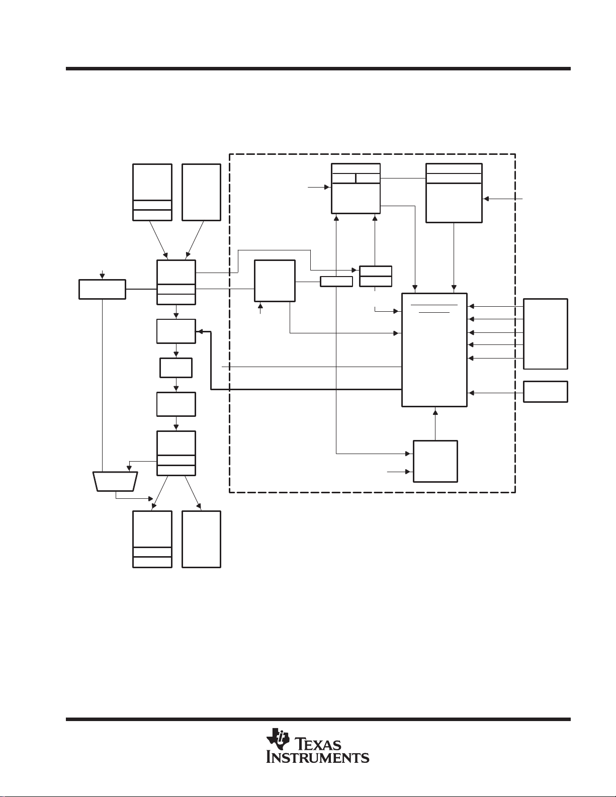
TNETX3270
ThunderSWITCH 24/3 ETHERNET SWITCH
WITH 24 10-MBIT/S PORTS AND 3 10-/100-MBIT/S PORTS
SPWS043B – NOVEMBER 1997 – REVISED APRIL 1999
frame routing
VLAN support
The internal routing engine supports the IEEE Std 802.1Q VLANs as shown in Figure 8 and described in the
following paragraphs.
If
rxacc
Header Inserted
If VLAN ID = 0x000
VLAN ID Replaced
Reset 0x0001
Source Port’s
PortxQtag
Inserted
VLAN ID
IEEE Std
802.1Q
Format
Frame
Header
= 1
Receive
Header
Possibly
Inserted
Header
Queue
Manager
RAM
Queue
Manager
Non-
IEEE Std
802.1Q
Format
Frame
Header
Inserted
VLAN ID
Lookup
Reset to
All 0s
Source Address (SA)
Destination Address (DA)
VLANnQID
Reset
1st Location:
0x001
All Others:
0x000
VLAN
Index
No Match
Source Port Number
Port Routing Code
VLAN ADDR
VLAN and
Ethernet
Addresses
Source
and
Destination
Lookups
VLAN
SA
DA
Unicast/
Multicast
Record
Number
No
Match
Frame-Routing
Algorithm
UnkUniPorts
UnkMultiPorts
UnkSrcPorts
UnkVLANPort
TxBlockPorts
RxUniBlockPorts
RxMultiBlockPorts
MirrorPort
UplinkPort
TrunkMapx
TrunkxPorts
NLearnPorts
Port Information
Port Numbers,
Time Stamps
Locked, Secure,
NBLCK, New
Port
Information
VLAN
Ports
Nauto
UnkVLAN
Lshare
Nage
Mirror
Disable
Reset is
Don’t Care
SysControl
All Ports
Portxcontrol
Compare
VLAN IDs
If (equal or
txacc
Then Strip Header,
= 1)
Otherwise,
Keep Header
IEEE Std
802.1Q
Format
Frame
Header
Header
Header
Retained
Transmit
Header
Stripped
Non-
IEEE Std
802.1Q
Format
Frame
IALE
Figure 8. VLAN Overview
Reset to
All 1s
VLANnPorts
POST OFFICE BOX 655303 • DALLAS, TEXAS 75265
39
Page 40

TNETX3270
ThunderSWITCH 24/3 ETHERNET SWITCH
WITH 24 10-MBIT/S PORTS AND 3 10-/100-MBIT/S PORTS
SPWS043B – NOVEMBER 1997 – REVISED APRIL 1999
IEEE Std 802.1Q headers – reception
When the internal address-lookup engine (IALE) examines the received frame, it contains an IEEE Std 802.1Q
header (after the source address). The header used depends on the port configuration. If the port is configured
as an access port, then IALE always uses the default VLAN ID (VID) programmed for this port. It accepts all
received frames on this port as untagged. If the frame already contains a header, it is tagged again. If the port
is programmed as a non-access port, then the header added depends on the received frame. If the frame is
not tagged, or the value of the header field is 0x000, then the default port VID is used to tag the frame internally .
Otherwise, the VID contained in the frame is used by the IALE.
The IALE does not support all 4096 VLAN IDs that can be encoded within the IEEE Std 802.1Q header at the
same time. The TNETX3270 has support for 32 VLANs, the VID in the received frame is compared with these
32 VLAN IDs to see which (if any) it matches. The designer can use any of the 4096 VLAN ID values for these
32 VLAN IDs.
unknown VLAN
If there is no match, then the rest of the address-lookup process is abandoned. A new VLAN interrupt is provided
to the attached CPU. The source address, VLAN ID, and port information is provided in internal registers so that
the CPU can determine if it wants to add this VID to the lookup table. If the destination address is unicast, then
the frame is discarded. If the destination address is multicast/broadcast, then the frame is forwarded based on
a programmable port mask.
known VLAN
If there is a match, the VLAN index associated with this VID together with the destination and source address,
are forwarded to the address-lookup and subsequent routing process. Only one of the VLAN IDs match if they
have been programmed correctly. If more than one matches, the hardware chooses one of them.
new VLAN member
The IALE checks to see if the source port already has been declared as a member of this VLAN. If not, then
an interrupt is provided to allow the attached CPU to add this port as a new member of the VLAN.
IEEE Std 802.1Q headers – transmission
The IEEE Std 802.1Q header is carried in the frame to the transmitting MAC port, where the decision to strip
out the header before transmission is made, based on the port configuration. If the port is configured as an
access port, the header is stripped before transmission. If the frame is only 64 bytes long, then 4 bytes of pad
(0s) are inserted between the end of the data and the start of the CRC word (a new CRC value is calculated
and inserted in the frame). If the port is configured as a non-access port, the VID is compared with the default
port VID. If they match, the header is stripped. Otherwise, the header is retained.
If the frame is transmitted to the NM port, then no header stripping occurs. The frame is transmitted unaltered.
It may contain one or two headers, depending on how the frame was originally received.
address maintenance
The addresses within the IALE can be maintained automatically by the TNETX3270, where addresses are
learned/updated from the wire and deleted, using one of two aging algorithms. Multicast addresses are not
automatically learned or aged. The attached CPU can add/update, find, or delete address records via the DIO
interface.
At times of peak activity, it may not be possible to learn or update every source address that is received. The
IALE backlogs up to one source address per port under these circumstances. Subsequent source addresses
received on a backlogged port are not learned/updated until that port’s backlog has been cleared. Lookups are
always given priority in the IALE, so these can never backlog.
The learning and aging processes are independent. This allows addresses to be learned automatically from the
wire, but allows the CPU to manage the aging process under software control.
40
POST OFFICE BOX 655303 • DALLAS, TEXAS 75265
Page 41

TNETX3270
ThunderSWITCH 24/3 ETHERNET SWITCH
WITH 24 10-MBIT/S PORTS AND 3 10-/100-MBIT/S PORTS
SPWS043B – NOVEMBER 1997 – REVISED APRIL 1999
spanning-tree support
Each port provides independent controls to block reception or transmission of frames, for learning of addresses,
or to disable the port on a per-port basis. Blocking can be overridden to allow reception or transmission of
spanning-tree frames.
aging algorithms
time-threshold aging
When processing (learning) addresses, the IALE adds the source address to the table and tags it with a time
stamp. If another frame is received with this source address, then the time stamp is refreshed. If the aging
counter expires before another frame is received from this source address, then the address is deleted from
the table. If the table is full, then the oldest address is deleted to make room for a new address, even if the age
for this address has not expired.
table-full aging
In table-full aging, the oldest address (or one of the oldest addresses if there is more than one) is automatically
deleted from the IALE records only if the table is full and a new address needs to be added to the table. In this
mode, the age stamp for the addresses is not refreshed.
frame-routing determination
When a frame is received, its 48-bit destination and source addresses are extracted and the VLAN index is
determined. The destination address and VLAN index are then looked up in the IALE records to determine if
a match exists. If a match is found, the information associated with the record is passed on to the frame-routing
algorithm. After removing disabled ports and checking for mirrored and trunking ports, the frame is sent to the
correct ports and the source address time stamp is reported.
The source address and VLAN index combination also are looked up in the IALE records to determine if a match
exists. If a match is found, additional information is provided to the routing process. Figure 9 provides a flow
diagram of the routing algorithm.
POST OFFICE BOX 655303 • DALLAS, TEXAS 75265
41
Page 42

TNETX3270
ThunderSWITCH 24/3 ETHERNET SWITCH
WITH 24 10-MBIT/S PORTS AND 3 10-/100-MBIT/S PORTS
SPWS043B – NOVEMBER 1997 – REVISED APRIL 1999
Start
Yes
Yes
Key:
interrupt
statistic
Unkmem
No
Yes No
Destination
Locked
Bit = 1?
No
Source Port
Blocked by
RxUniBlockPorts
and Dest.
Nblck=0?
No No No No No
Destination
Multicast?
Source Port
Blocked by
RxMultiBlockPorts
Yes
is
Yes Yes
and Dest.
Nblck=0?
Known
VLAN?
Yes
Source Port = 1 in.
VLANnports?
Yes
Destination
Address
Found?
Yes
UnkVLAN
Destination
is
Multicast?
Source Port
Blocked by
RxMultiBlockPorts?
No
NoNo
RxUniBlockPorts?
Yes
Source Port
Blocked by
Destination
Multicast?
Source Port
Blocked by
RxMultiBlockPorts or
UnkVLAN=0?
Yes
is
Yes
No
Set Port Routing
Code to 0
To C
(Continued)
Port Routing
Code = Port Code
From Records
Destination
Cuplink Bit
Set?
No
Yes
Port Routing
Code = Port Vector
From Records
Include UplinkPort
in Port
Routing Code
To A
(Continued)
Port Routing
Code =
UnkMultiPorts
Unknown
Multicast
Destination
AND Port Routing
Code With VLAN
VLANnports Code
Figure 9. Frame-Routing Algorithm
Port Routing
Code =
UnkUniPorts
Unknown
Unlcast
Destination
Port Routing
Code =
UnkVLANPort
To B
(Continued)
42
POST OFFICE BOX 655303 • DALLAS, TEXAS 75265
Page 43

TNETX3270
ThunderSWITCH 24/3 ETHERNET SWITCH
WITH 24 10-MBIT/S PORTS AND 3 10-/100-MBIT/S PORTS
SPWS043B – NOVEMBER 1997 – REVISED APRIL 1999
A B
Discard
Frame
Yes
secvio
Source
Port
Security
Violation
Source
Secure
Bit = 1?
No
chng
Yes
No
Source
Address
Found?
Yes
Source
Locked
Bit = 1?
No
Source
Port
Moved?
Yes
Stayed
Within a
Trunk?
Yes
Yes
Source
Port = 1 in
RingPorts?
Yes
No
No
Source
Port = 1 in
NLearnPorts?
Yes
new
No
AND UnkSrcPorts
With VLAN
VLANnports,
Then OR With
Port Routing Code
Unknown
Source
No
Remove Source Port
(and other trunk members)
From
Port Routing Code
To C
(Continued)
Figure 9. Frame-Routing Algorithm (Continued)
POST OFFICE BOX 655303 • DALLAS, TEXAS 75265
43
Page 44

TNETX3270
ThunderSWITCH 24/3 ETHERNET SWITCH
WITH 24 10-MBIT/S PORTS AND 3 10-/100-MBIT/S PORTS
SPWS043B – NOVEMBER 1997 – REVISED APRIL 1999
DC
Remove:
– Disabled Ports
– Ports Blocked by TxBlockPorts
From Port Routing Code
E
Mirr
Bit = 1?
No
Lshare = 1?
No
Port Routing Code
is Adjusted by
Trunking Algorithm
(see Note A)
Yes
Yes
If
((Source Port = MirrorPort or
Port Routing Code Includes MirrorPort)
and (Source Port ! = UplinkPort))
Then
Include UplinkPort in Port Routing Code
Destination
Found?
Yes
No
Port Routing Code
is Adjusted by
Load-Sharing
Algorithm
(see Note A)
NOTE A: See
Port Trunking/Load Sharing
Port Routing
Code = 0?
No
Send Frame to
Ports Indicated by
Port Routing Code
Yes
Discard
Frame
Figure 9. Frame-Routing Algorithm (Continued)
port mirroring
The TNETX3270 allows all transmitted frames on a particular port to be copied (or mirrored) to a designated
port.
44
POST OFFICE BOX 655303 • DALLAS, TEXAS 75265
Page 45

TNETX3270
ThunderSWITCH 24/3 ETHERNET SWITCH
WITH 24 10-MBIT/S PORTS AND 3 10-/100-MBIT/S PORTS
SPWS043B – NOVEMBER 1997 – REVISED APRIL 1999
port trunking/load sharing
Port trunking is a technique that allows two or more ports to be parallel connected between switches and
counted as one port to increase the bandwidth between those devices. The trunking algorithm determines on
which of these ports a frame is transmitted, spreading the load evenly across these ports and maintaining packet
order.
The TNETX3270 supports trunking on the 10-/100-Mbit/s ports. Trunk-port determination is the final step in the
IALE frame-routing algorithm. Once the destination port(s) for a frame has been determined, the port-routing
code is examined to see if any of the destination ports are members of the trunk. If so, the trunking algorithm
is applied to select which port within that trunk transmits the frame – it may or may not be the one currently in
the port-routing code. To determine the destination port within a trunk, bits 3–1 of the source and destination
address are XORed to produce a map index. This map index is used to index to a group of eight internal registers
to determine the destination port. The actual transmit port of a unicast packet is dynamic, based on the eight
internal registers.
Load sharing is similar to trunking, with the following differences:
D
If the destination address was found in the IALE records when it was looked up, the port-routing code is not
adjusted by the load-sharing/-trunking algorithm.
D
The 3-bit map index is determined only from the source address as follows:
– Bits 47–32 are XORed to produce the most significant bit of the map index.
– Bits 31–16 are XORed to produce the middle of the map index.
– Bits 15–0 are XORed to produce the least significant bit of the map index.
Once assigned, the tx port for a unicast packet is static.
flow control
The switch incorporates two forms of flow control: collision based, and IEEE Std 802.3 pause frames.
In either case, the switch recognizes when it is becoming congested by monitoring the size of the free-buffer
queue. When the number of free buffers drops below the specified threshold, the switch prevents frames from
entering the device by issuing the flow control appropriate to each port’s current mode of operation. This
prevents reception of any more frames on those ports until the frame backlog is reduced and the number of free
buffers has risen above the threshold, at which point flow control ceases and frames again can be received.
The default free-buffer threshold after a hardware reset is chosen to ensure that all ports simultaneously can
start reception of a maximum-length frame and ensure complete reception.
The purpose of flow control is to reduce the risk of data loss if a long burst of activity caused the switch to backlog
frames to the point where the memory system is full. However, there is no way to prevent frame reception on
those ports operating in full-duplex mode that have not negotiated IEEE Std 802.3 flow control. Such ports can
exhaust the free buffer queue, with subsequent data loss.
Each 10-/100-Mbit/s port can request collision or IEEE Std 802.3X flow control through internal registers.
Flow control is globally enabled/disabled. Each individual port can request half- or full-duplex or IEEE Std 802.3
flow to be negotiated by the PHY device.
In full duplex, a port does not start transmitting a new frame if the collision pin is active, although the value of
this pin is ignored at other times.
POST OFFICE BOX 655303 • DALLAS, TEXAS 75265
45
Page 46

TNETX3270
ThunderSWITCH 24/3 ETHERNET SWITCH
WITH 24 10-MBIT/S PORTS AND 3 10-/100-MBIT/S PORTS
SPWS043B – NOVEMBER 1997 – REVISED APRIL 1999
collision-based flow control
Collision-based flow control provides a means of preventing frame reception for ports that are operating in
half-duplex mode. While the number of free buffers is fewer than the specified threshold, ports in this state that
are not currently transmitting generate collisions when they start to receive a frame. The jam sequence
transmitted (55.55.55.55.55.55.55.5D.DD.DD.DD.DD (hex) starts approximately when the source address
starts to receive. Port 8 begins jam sequence after approximately eight bytes of payload data (i.e., after the
source address) have been received.
These forced collisions are not limited to a maximum of 16 consecutive collisions, and are independent of the
normal backoff algorithm.
IEEE Std 802.3 flow control
IEEE Std 802.3X flow control provides a means of reducing network congestion on ports that are operating in
full duplex mode, via special pause frames. It is symmetrical, so that devices that transmit pause frames also
must respond to received pause frames.
Pause frames and their behavior are fully described in the IEEE Std 802.3X standard, but in essence they
comprise:
D
48-bit multicast destination address 01.80.C2.00.00.01
D
48-bit source address – is read from the Devnode register when transmitted by this device.
D
16-bit length/type field, containing the value 88.08
D
16-bit pause opcode equal to 00.01
D
16-bit pausetime. This specifies a nonzero number of pausequanta. A pausequantum is 512 bit times.
D
Padding as required/desired
D
32-bit frame-check sequence (CRC word)
All quantities above are hexadecimal and are transmitted most significant byte first. Within the byte they are
transmitted least significant bit first.
The padding is required to fill out the frame to a minimum of 64 bytes. The standard allows pause frames longer
than 64 bytes to be discarded or interpreted as valid pause frames. This device recognizes any pause frame
that is between 64 bytes and 1531 bytes long. It always transmits 64-byte pause frames.
Each 10-/100-Mbit/s port can request IEEE Std 802.3X pause-frame support via the reqnp (= 0) bit within its
Portxcontrol register. The 100-/1000-Mbit/s port has independent control for transmission and reception of IEEE
Std 802.3X pause frames, and can request IEEE Std 802.3X flow control via the reqntxp (= 0) and reqnrxp (= 0)
bits within its Portxcontrol.
Outgoing pause frames are issued only when:
D
pause (10/100) = 1
D
The port is operating in the full-duplex mode.
D
flow = 1 in Syscontrol
Incoming pause frames are acted on only when:
46
D
pause = 1 or pausetx = 1 (i.e., incoming pause frames are recognized in both full-duplex and half-duplex
modes, regardless of the value of the flow bit)
POST OFFICE BOX 655303 • DALLAS, TEXAS 75265
Page 47

TNETX3270
ThunderSWITCH 24/3 ETHERNET SWITCH
WITH 24 10-MBIT/S PORTS AND 3 10-/100-MBIT/S PORTS
SPWS043B – NOVEMBER 1997 – REVISED APRIL 1999
pause frame reception
The IEEE Std 802.3X standard defines a MAC control frame as any frame containing a length/type value = 88.08
(hex). This device always absorbs (i.e., discards) within the MAC all such frames that it receives, regardless
of the configuration of the port (i.e., pause and duplex have no effect on this behavior). MAC control frames are
not forwarded to any other port and are
MAC statistics in the same manner as data frames, but are not seen by the IALE, so do not appear in its statistics
(i.e., receive filtered frames, security violations, unknown unicast destination, unknown multicast destination,
or unknown source).
Pause frames are the subset of MAC control frames with the opcode field = 0x0001. These are acted on by a
port only if:
D
pause = 1 in its Portxstatus register
D
The frame’s length is 64–1531 bytes, inclusive.
D
MxxRXER does not go active at any time during its reception.
D
Its FCS passes the CRC.
The pause_time value from such valid frames is extracted from the two bytes following the opcode. This is
loaded into the port’s pause timer and the pause_time period is timed.
not used by IALE for learning source addresses. They appear in the
If a valid pause frame is received during the pause_time period of a previous pause frame:
D
If its destination address is not equal to the reserved multicast address or the address in the Devnode
register, the pause timer immediately expires.
D
If the new pause_time value is 0, the pause timer immediately expires.
D
If the pause timer within the port immediately is set to the pause_time value of the new pause frame (any
remaining pause time from the previous pause frame is disregarded).
If the pause bit in Portxstatus ever becomes a 0 (because pause frames are no longer supported), the pause
timer immediately expires.
A port does not begin to transmit any new data frame any later than 512-bit times after a pause frame with a
nonzero pause time has been received (RXDV going inactive). It does not begin to transmit any data frame until
the pause timer has expired. (However, it can transmit pause frames of its own if it needs to initiate flow control).
Any frame already in mid-transmission when a pause frame is received is unaffected; it completes transmission
as normal.
pause frame transmission
When the number of free buffers within the switch becomes less than the number specified in Flowthreshold,
full-duplex ports that have had pause frames negotiated/enabled transmit a pause frame at the first available
opportunity (immediately if currently idle, or following completion of the frame currently being transmitted). The
pause frame contains the pausetime field from Pausetimex register that matches the current operating speed
of the port.
If the number of free buffers still is less than the number specified in Flowthreshold after 80% of the time interval
represented by the respective pausetime field has elapsed, then another pause frame is transmitted at the
earliest opportunity.
If the value in Pausetimex is 0, then no pause frames are transmitted on ports with that speed.
It is anticipated that the pausetime values for the different port speeds will be programmed to have a 10:1 ratio,
so that different-speed ports pause for the same amount of real time.
Note that transmitted pause frames are only a request to the other end station to stop transmitting. Frames that
are received during the pause interval are received normally (provided the buffer memory is not full).
POST OFFICE BOX 655303 • DALLAS, TEXAS 75265
47
Page 48

TNETX3270
ThunderSWITCH 24/3 ETHERNET SWITCH
WITH 24 10-MBIT/S PORTS AND 3 10-/100-MBIT/S PORTS
SPWS043B – NOVEMBER 1997 – REVISED APRIL 1999
pause frame transmission (continued)
Pause frames are transmitted if required, even if the port is observing the pausetime period from a pause frame
it has received.
internal wrap test
Internal wrap mode causes some or all of the Ethernet MACs to be configured to loop back transmitted data
into the receive path. This allows a frame to be sent into a designated source port and then selectively routed
successively to and from ports involved in the test, before finally transmitting the frame out of the original port.
By varying the number of ports between which the frame is forwarded, the potential fault capture area is
expanded or constrained.
Intwrap in Systest determines which ports loop back. Ports 0 or 8 can be configured to not loop back, allowing
them to be used as the start/end port for the test. Alternatively, the NM port (accessed via DIO) can be used
for this purpose, with all MII ports configured to loop back.
For a frame to be forwarded from one port to another in this fashion, the switch must be programmed as follows:
D
Assign a unique VID to each of the PortxQtag registers, and program these tags into the VLANnQID
registers.
D
The VLANnports register associated with each of the VLANnQID registers should have only one bit set,
indicating the port to which frames containing that IEEE Std 802.3 tag should be routed.
D
Rxacc and Txacc for each port must be 1. This causes the port to add the VID from its PortxQtag to the frame
on reception, and strip the tag before transmission.
D
The destination address of the frames to be applied is not known, and UnkUniPorts and UnkMultiPorts
should be all 1s.
This causes the following:
1. The VID from the source port PortxQtag register is added to the frame upon reception. As the address of
the frame is unknown, it is forwarded to the AND of the appropriate VLANnports and Unkuniports (unicast)
or Unkmultiports (multicast). As VLANnports should contain only a single 1, this should be a single port.
2. The frame is transmitted from the destination port selected in 1. Its VLAN tag is stripped beforehand; the
frame loops back to the receive path.
3. Steps 1 and 2 are repeated, but the VID added upon reception is different from the one just stripped off at
transmission. This means a different VLANnports register is used to determine the destination.
4. Eventually, the frame is sent to a port that is not configured for loopback and leaves the switch.
The operational status of the PHYs or external connections to the device do not have to be considered or
assumed good when in internal loopback mode.
48
POST OFFICE BOX 655303 • DALLAS, TEXAS 75265
Page 49

TNETX3270
ThunderSWITCH 24/3 ETHERNET SWITCH
WITH 24 10-MBIT/S PORTS AND 3 10-/100-MBIT/S PORTS
SPWS043B – NOVEMBER 1997 – REVISED APRIL 1999
08
07
06
05
04 03 02 01 00
09 26
TNETX3270
NM
Figure 10. Internal Wrap Example
duplex wrap test
Duplex wrap test is similar to internal wrap mode (see Figure 11). The ports can be set to accept frame data
that is wrapped at the PHY. This permits network connections between the device and the PHY to be verified.
Any port can be the source port (not just the NM port as shown in Figure 10). By using multicast/broadcast
frames, traffic can be routed selectively between ports involved in the test or return the frame directly before
retransmission on the uplink. Software control of the external PHYs is required to configure them for loopback.
If the internal PCS is in use (port configured in PMA mode) loopback in PCSxcontrol also must be asserted. This
causes MxxEWRAP to be high, forcing external PMD into loopback mode.
Duplex frame-wrap test mode is selected by setting dpwrap in Systest. When selected, the port is forced into
full duplex, allowing it to receive frames it transmits.
The switch is configured in the same manner as internal wrap.
PHY
PHY
08
07
06
05
04 03 02 01 00
09 26
TNETX3270
NM
Figure 11. Duplex Wrap Example
POST OFFICE BOX 655303 • DALLAS, TEXAS 75265
49
Page 50

TNETX3270
ThunderSWITCH 24/3 ETHERNET SWITCH
WITH 24 10-MBIT/S PORTS AND 3 10-/100-MBIT/S PORTS
SPWS043B – NOVEMBER 1997 – REVISED APRIL 1999
port mirroring
It is possible to copy (or mirror) all frames that are received by and transmitted to a port designated by the
Mirrorport register to the port designated by the Uplinkport register. This feature is enabled if the mirr bit in
Syscontrol is set to 1, and disabled if it is 0.
If Mirrorport selects a port that is a member of a trunk, only that single specific port is mirrored. Frame traffic
on the other trunk port(s) is not mirrored. The Uplinkport register should not select a port within a trunk
(undesired behavior can occur if this is done).
copy to uplink
If destination address is a unicast and the cuplnk bit of its address record is set to 1 (via a DIO add), when a
frame specifies that address as the destination, a copy of the frame also is sent to the port specified in the
Uplinkport register. The Uplinkport register should not be set to select a port within a trunk (undesired behavior
can occur if this is done).
50
POST OFFICE BOX 655303 • DALLAS, TEXAS 75265
Page 51

TNETX3270
ThunderSWITCH 24/3 ETHERNET SWITCH
WITH 24 10-MBIT/S PORTS AND 3 10-/100-MBIT/S PORTS
SPWS043B – NOVEMBER 1997 – REVISED APRIL 1999
absolute maximum ratings over operating junction temperature range (unless otherwise noted)
Supply voltage range: V
Input voltage range, V
Output voltage range, V
DD(2.5V)
V
DD(3.3V)
: Standard –0.5 V to V
I
: Standard –0.5 V to V
O
Thermal impedance: Junction-to-ambient package, airflow = 0, Z
Junction-to-ambient package, airflow = 150 fpm, Z
Junction-to-case package, 0 Z
Operating case temperature range, T
Storage temperature range, T
†
Stresses beyond those listed under “absolute maximum ratings” may cause permanent damage to the device. These are stress ratings only, and
functional operation of the device at these or any other conditions beyond those indicated under “recommended operating conditions” is not
implied. Exposure to absolute-maximum-rated conditions for extended periods may affect device reliability.
NOTES: 1. Applies to external input buffers. Level-shifting inputs are relative to V
2. Applies to external output buffers. Level-shifting outputs are relative to V
–0.5 V to 2.7 V. . . . . . . . . . . . . . . . . . . . . . . . . . . . . . . . . . . . . . . . . . . . . . . . . . .
–0.5 V to 3.6 V. . . . . . . . . . . . . . . . . . . . . . . . . . . . . . . . . . . . . . . . . . . . . . . . . . .
15°C/W. . . . . . . . . . . . . . . . . . . . . . . . . .
θJA
1.08°C/W. . . . . . . . . . . . . . . . . . . . . . . . . . . . . . . . . . .
0°C to 95°C. . . . . . . . . . . . . . . . . . . . . . . . . . . . . . . . . . . . . . . . . . . . . . . .
C
–65°C to 150°C. . . . . . . . . . . . . . . . . . . . . . . . . . . . . . . . . . . . . . . . . . . . . . . . . . .
stg
θJC
DD(3.3V)
DD(3.3V)
11.5°C/W. . . . . . . . . . . . . . . . . . .
θJA
.
.
DD(3.3V)
DD(2.5V)
+ 0.4 V. . . . . . . . . . . . . . . . . . . . . . . . . . . . . . . . . . . . . . . .
+ 0.5 V. . . . . . . . . . . . . . . . . . . . . . . . . . . . . . . . . . . . . .
recommended operating conditions
MIN NOM MAX UNIT
V
DD(2.5V)
V
DD(3.3V)
V
IH
V
IL
I
OH
I
OL
Supply voltage 2.3 2.5 2.7 V
Supply voltage 3 3.3 3.6 V
High-level dc input voltage 2.3 3.3 V
Low-level dc input voltage 0 0.65 V
High-level output current –2 mA
Low-level output current –2 mA
†
electrical characteristics over recommended operating conditions (unless otherwise noted)
PARAMETER TEST CONDITIONS MIN TYP MAX UNIT
V
OH
V
OL
I
IH
I
IL
I
OZ
I
DD(2.5V)
I
DD(3.3V)
C
i
C
o
High-level output voltage IOH = rated 2.5 V
Low-level output voltage IOL = rated 0.5 V
High-level input current VI = V
Low-level input current VI = GND –1 µA
High-impedance-state output current VO = V
Supply current V
Supply current V
Capacitance, input 6 pF
Capacitance, output 6 pF
DD(3.3V)
DD(3.3V)
DD(2.5V)
DD(3.3V)
, VO = 0 ±10 µA
= max, f = 83.33 MHz 1.5 A
= max, f = 83.33 MHz 0.175 A
1 µA
POST OFFICE BOX 655303 • DALLAS, TEXAS 75265
51
Page 52

TNETX3270
ThunderSWITCH 24/3 ETHERNET SWITCH
WITH 24 10-MBIT/S PORTS AND 3 10-/100-MBIT/S PORTS
SPWS043B – NOVEMBER 1997 – REVISED APRIL 1999
PARAMETER MEASUREMENT INFORMATION
Outputs are driven to a minimum high-logic level of 3.3 V and to a maximum low-logic level of 0 V.
Output transition times are specified as follows: For a high-to-low transition on either an input or output signal, the
level at which the signal is said to be no longer high is 1.4 V and the level at which the signal is said to be low is 1.4 V .
For a low-to-high transition, the level at which the signal is said to be no longer low is 0.8 V and the level at which
the signal is said to be high is 2 V, as shown in the following.
The rise and fall times are not specified but are assumed to be those of standard TTL devices, which are typically
1.5 ns.
1.4 V
test measurement
The test-and-load circuit shown in Figure 12 represents the programmable load of the tester pin that is used
to verify timing parameters of the TNETX3270 output signals.
I
OL
2 V (high)
0.8 V (low)
Where: I
Test
Point
V
LOAD
C
I
OH
TTL OUTPUT TEST LOAD
= Refer to IOL in recommended operating conditions.
OL
I
= Refer to IOH in recommended operating conditions.
OH
= 1.5 V, typical dc-level verification or
V
LOAD
C
L
1.5 V, typical timing verification
= 45 pF, typical load-circuit capacitance
TTL
Output
Under
Test
L
Figure 12. Test-and-Load Circuit
52
POST OFFICE BOX 655303 • DALLAS, TEXAS 75265
Page 53

TNETX3270
ThunderSWITCH 24/3 ETHERNET SWITCH
WITH 24 10-MBIT/S PORTS AND 3 10-/100-MBIT/S PORTS
SPWS043B – NOVEMBER 1997 – REVISED APRIL 1999
10-Mbit/s interface (ports 00–23)
timing requirements (see Notes 3 through 6 and Figure 13)
NO. MIN MAX UNIT
1 t
c(THxCLK)
2 T
w(THxCLK)
3 t
su(THxSYNC)
4 t
su(THxCOL)
4 t
su(THxCRS)
4 t
su(THxLINK)
4 t
su(THxRXD)
4 t
su(THxRXDV)
5 t
h(THxSYNC)
6 t
h(THxCOL)
6 t
h(THxCRS)
6 t
h(THxLINK)
6 t
h(THxRXD)
6 t
h(THxRXV)
t
r(THxCLK)
t
†
NOTES: 3. The TNETE2008 must supply at least two THxSYNC pulses under normal conditions before driving valid data on the inputs to the
f(THxCLK)
THx = TH0, TH1, and TH2
4. At least two clocks must be driven before the deassertion of the system reset signal, and a minimum of two clocks must be driven
5. For receive data, the TNETE2008 asserts the THxCOL signal during the appropriate slot time if it was asserted for any of the four
6. For receive data, the TNETE2008 asserts the THxRXDV signal only if there are four valid bits of data in the nibble.
†
Cycle time, THxCLK 50 58 ns
Pulse duration, THxCLK high or low 23 27 ns
Setup time, THxSYNC high before THxCLK↓ 8 ns
Setup time, THxCOL high before THxCLK↑ 8 ns
Setup time, THxCRS high before THxCLK↑ 8 ns
Setup time, THxLINK high before THxCLK↑ 8 ns
Setup time, THxRXD3–THxRXD0 valid before THxCLK↑ 8 ns
Setup time, THxRXDV high before THxCLK↑ 8 ns
Hold time, THxSYNC high after THxCLK↓ 8 ns
Hold time, THxCOL high after THxCLK↑ 8 ns
Hold time, THxCRS high after THxCLK↑ 8 ns
Hold time, THxLINK high after THxCLK↑ 8 ns
Hold time, THxRXD3–THxRXD0 valid after THxCLK↑ 8 ns
Hold time, THxRXDV high after THxCLK↑ 8 ns
Rise time, THxCLK 2 ns
Fall time, THxCLK 2 ns
TNETX3270, or before expecting valid data on the outputs from the TNETX3270. This means that at least two full sequences must
be executed; only with the third THxSYNC pulse is valid data presented/expected.
after the deassertion of the the system reset signal to ensure complete initialization of the internal circuitry of the TNETX3270 before
there is any valid activity across the interface.
bits of data corresponding to that slot time.
operating characteristics over recommended operating conditions (see Notes 3 through 6 and
Figure 13)
NO. PARAMETER MIN MAX UNIT
7 t
d(THxEN)
7 t
d(THxTXD)
7 t
d(THxRENEG)
8 t
d(THxTXEN)
8 t
d(THxTXD)
8 t
†
NOTES: 3. The TNETE2008 must supply at least two THxSYNC pulses under normal conditions before driving valid data on the inputs to the
d(THxRENEG)
THx = TH0, TH1, and TH2
4. At least two clocks must be driven before the deassertion of the system reset signal, and a minimum of two clocks must be driven
5. For receive data, TNETE2008 asserts the THxCOL signal during the appropriate slot time if it was asserted for any of the four bits
6. For receive data, the TNETE2008 asserts the THxRXDV signal only if there are four valid bits of data in the nibble.
†
Delay time, from THxCLK↑ to THxTXEN↑ 13.5 ns
Delay time, from THxCLK↑ to THxTXD3–THxTXD0 valid 13.5 ns
Delay time, from THxCLK↑ to THxRENEG↓ 13.5 ns
Delay time, from THxCLK↑ to THxTXEN↓ 0 ns
Delay time, from THxCLK↑ to THxTXD3–THxTXD0 invalid 0 ns
Delay time, from THxCLK↑ to THxRENEG↑ 0 ns
TNETX3270, or before expecting valid data on the outputs from the TNETX3270. This means that at least two full sequences must
be executed; only with the third THxSYNC pulse is valid data presented/expected.
after the deassertion of the the system reset signal to ensure complete initialization of the internal circuitry of the TNETX3270 before
there is any valid activity across the interface.
of data corresponding to that slot time.
POST OFFICE BOX 655303 • DALLAS, TEXAS 75265
53
Page 54

TNETX3270
ThunderSWITCH 24/3 ETHERNET SWITCH
WITH 24 10-MBIT/S PORTS AND 3 10-/100-MBIT/S PORTS
SPWS043B – NOVEMBER 1997 – REVISED APRIL 1999
1
THxCLK
(input)
2 2
THxSYNC
(input)
THxCOL
THxCRS
THxLINK
THxRXD3–THxRXD0
THxRXDV
(inputs)
THxTXEN
THxTXD3–THxTXD0
THxRENEG
(outputs)
10-/100-Mbit/s MAC interface
7
Figure 13. 10-Mbit/s Interface (Ports 00–23)
53
64
8
Figures 14 and 15 show the timings at 100 Mbit/s and 10 Mbit/s for the 10-/100-Mbit/s port interfaces to the
TNETE2101 devices.
10-/100-Mbit/s receive ports (24, 25, 26)
timing requirements (see Note 7 and Figure 14)
NO. MIN MAX UNIT
1 t
c(MxxRCLK)
2 t
w(MxxRCLKL)
3 t
w(MxxRCLKH)
4†t
su(MxxRXD)
4†t
su(MxxRXDV)
4†t
su(MxxRXER)
5†t
h(MxxRXD)
5†t
h(MxxRXDV)
5†t
†
xx = ports 24, 25, and 26
NOTE 7: Both MxxCRS and MxxCOL are driven asynchronously by the PHY. MxxRXD3–MxxRXD0 is driven by the PHY on the falling edge of
h(MxxRXER)
MxxRCLK. MxxRXD3–MxxRXD0 timing must be met during clock periods when MxxRXDV is asserted. MxxRXDV is asserted and
deasserted by the PHY on the falling edge of MxxRCLK. MxxRXER is driven by the PHY on the falling edge of MxxRCLK.
Cycle time, MxxRCLK 25 25 ns
Pulse duration, MxxRCLK low ns
Pulse duration, MxxRCLK high 14 ns
Setup time, MxxRXD3–MxxRXD0 valid before MxxRCLK↑ 5 ns
Setup time, MxxRXDV valid before MxxRCLK↑ 5 ns
Setup time, MxxRXER valid before MxxRCLK↑ 5 ns
Hold time, MxxRXD3–MxxRXD0 valid after MxxRCLK↑ 5 ns
Hold time, MxxRXDV valid after MxxRCLK↑ 5 ns
Hold time, MxxRXER valid after MxxRCLK↑ 5 ns
1
4 5
2 2
MxxRCLK
(input)
54
MxxRXD3–MxxRXD0
MxxRXDV
MxxRXER
(inputs)
Figure 14. 10-/100-Mbit/s Receive Ports
POST OFFICE BOX 655303 • DALLAS, TEXAS 75265
Page 55

TNETX3270
ThunderSWITCH 24/3 ETHERNET SWITCH
WITH 24 10-MBIT/S PORTS AND 3 10-/100-MBIT/S PORTS
SPWS043B – NOVEMBER 1997 – REVISED APRIL 1999
10-/100-Mbit/s transmit ports (24, 25, and 26)
timing requirements (see Figure 15)
NO. MIN MAX UNIT
1 t
c(MxxTCLK)
2 t
w(MxxTCLKL)
3 t
w(MxxTCLKH)
operating characteristics over recommended operating conditions (see Note 8 and Figure 15)
NO. PARAMETER MIN MAX UNIT
4†t
d(MxxTXD)
4†t
d(MxxTXEN)
4†t
†
NOTE 8: Both MxxCRS and MxxCOL are driven asynchronously by the PHY. MxxTXD3–MxxTXD0 is driven by the reconciliation sublayer
d(MxxTXER)
xx = ports 24, 25, and 26
synchronous to the MxxTCLK. MxxTXEN is asserted and deasserted by the reconciliation sublayer synchronous to the MxxTCLK rising
edge. MxxTXER is driven synchronous to the rising edge of MxxTCLK.
Cycle time, MxxTCLK 25 25 ns
Pulse duration, MxxTCLK low ns
Pulse duration, MxxTCLK high 14 ns
Delay time, from MxxTCLK↑ to MxxTXD3–MxxTXD0 valid 0 25 ns
Delay time, from MxxTCLK↑ to MxxTXEN valid 0 25 ns
Delay time, from MxxTCLK↑ to MxxTXER valid 0 25 ns
1
4
2 3
MxxTCLK
(input)
MxxTXD3–MxxTXD0
MxxTXEN
MxxTXER
(outputs)
Figure 15. 10-/100-Mbit/s Transmit Ports
POST OFFICE BOX 655303 • DALLAS, TEXAS 75265
55
Page 56

TNETX3270
Î
ThunderSWITCH 24/3 ETHERNET SWITCH
WITH 24 10-MBIT/S PORTS AND 3 10-/100-MBIT/S PORTS
SPWS043B – NOVEMBER 1997 – REVISED APRIL 1999
SDRAM interface
The SDRAM interface observes two types of timing:
D
Multicycle timings between commands
D
Subcycle timings between signals and DCLK
Figure 16 illustrates the SDRAM interfaces signal timing in which each type of SDRAM command and its
interrelated timings are shown. It is not intended to be representative of any particular receive or transmit buffer
operation.
SDRAM command to command (see Figure 16)
SYMBOL PARAMETER MIN MAX UNIT
t
RSA
t
RC
t
RAS
t
RP
t
RCD
t
AC3
n
CCD
n
CWL
t
RWD
t
WR
MRS to ACTV or REFR 24 ns
Row cycle time (ACTV to REFR to next ACTV or REFR) 120 ns
Row active time (ACTV to DCAB) 72 ns
Row recharge time (DCAB to ACTV, REFR, or MRS) 36 ns
Row to column delay (ACTV to READ or WRT) 36 ns
Column access time [READ (CAS) latency] (READ to data sample) 36 ns
Column address to column address (WRT to next READ or WRT, or READ to next READ) 24 ns
Last data or write to new column address (WRT to next READ or WRT) 24 ns
Read to write delay (READ to next WRT) 60 ns
Write recovery time (WRT to DCAB) 24 ns
DCLK
DRAS
DCAS
DW
DD31–DD00
DA13–DA00
REGISTER
SETTINGS
t
RSA
NOOP NOOP
MODE ROW READ1 WRITE READ2 XXXX
t
t
RWD
RC
n
n
NOOP
NOOP
t
RAS
t
RCD
ACTV
NOOP NOOP
READ READ
BUFFOP READ1 WRITE
DA10=0 DA10=0 DA10=1DA10=0
t
AC3
NOOP
Figure 16. SDRAM Command to Command
CWL
CCD
WRT
t
WR
DCAB
t
AC3
NOOP
t
RP
NOOPMRS
REFRNOOP
READ2
56
POST OFFICE BOX 655303 • DALLAS, TEXAS 75265
Page 57
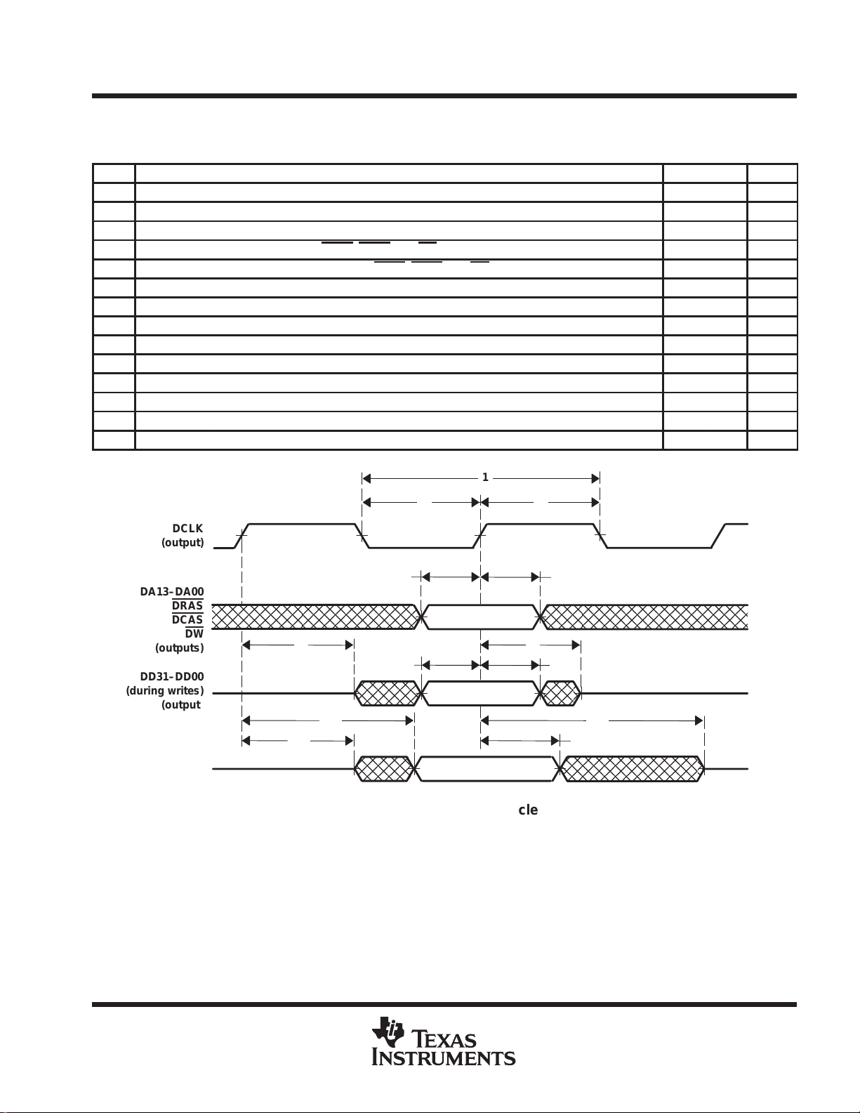
ООООООО
ОООООООООО
ThunderSWITCH 24/3 ETHERNET SWITCH
WITH 24 10-MBIT/S PORTS AND 3 10-/100-MBIT/S PORTS
SPWS043B – NOVEMBER 1997 – REVISED APRIL 1999
SDRAM subcycle
operating characteristics over recommended operating conditions (see Figure 17)
NO.
1 t
2 t
3 t
4 t
5 t
6 t
7 t
8 t
9 t
10 t
11 t
12 t
13 t
c(DCLK)
w(DCLKL)
w(DCLKH)
d(DCLK)
d(DA)
en(DDW)
en(DDR)
dis(DDW)
dis(DDR)
d(DDW)1
d(DDW)2
d(DDR)1
d(DDR)2
t
t
Cycle time, DCLK 12 12 ns
Pulse duration, DCLK low 5 ns
Pulse duration, DCLK high 5 ns
Delay time, from DA, DRAS, DCAS, and DW valid to DCLK↑ 4 ns
Delay time, from DCLK↑ to DA, DRAS, DCAS, and DW invalid 2 ns
Enable time, from DCLK↑ to before DD31–DD00 driven (write cycle) 0 ns
Enable time, from DCLK↑ to before DD31–DD00 driven (read cycle) 0 ns
Disable time, from DCLK↑ to after DD31–DD00 (after final write cycle) to Z state 10 ns
Disable time, from DCLK↑ to after DD31–DD00 (after final read cycle) to Z state 11 ns
Delay time, from DD valid to DCLK↑ (write cycle) 4 ns
Delay time, from DCLK↑ to DD31–DD00 Z state (write cycle) 2 ns
Delay time, from DCLK↑ to DD31–DD00 valid (read cycle) 10 ns
Delay time, from DCLK↑ to DD31–DD00 invalid (read cycle) 0 ns
Transition time, rise and fall, all signals 1 4 ns
PARAMETER MIN MAX UNIT
TNETX3270
DCLK
(output)
DA13–DA00
DRAS
DCAS
DW
(outputs)
DD31–DD00
(during writes)
(output)
DD31–DD00
(during reads)
(input)
1
2 3
4 5
6
10
Z
12 9
Z
8
11
Z
137
Z
Figure 17. SDRAM Subcycle
POST OFFICE BOX 655303 • DALLAS, TEXAS 75265
57
Page 58

TNETX3270
ThunderSWITCH 24/3 ETHERNET SWITCH
WITH 24 10-MBIT/S PORTS AND 3 10-/100-MBIT/S PORTS
SPWS043B – NOVEMBER 1997 – REVISED APRIL 1999
DIO/DMA interface
The DIO interface is asynchronous to allow easy adaptation to a range of microprocessor devices and computer
system interfaces.
DIO/DMA write cycle
timing requirements (see Figure 18)
NO. MIN MAX UNIT
1 t
w(SCSL)
2 t
w(SCSH)
3 t
su(SRNW)
4 t
su(SAD)
5 t
su(SDATA)
operating characteristics over recommended operating conditions (see Figure 18)
NO. PARAMETER MIN MAX UNIT
6 t
w(SRDYH)
7 t
d(SRNW)
8 t
d(SAD)
9 t
d(SDATA)
10 t
d(SCS)
11 t
d(SRDY)1
12 t
d(SRDY)2
13 t
†
d(SRDY)3
When the switch is performing certain internal operations (e.g., EEPROM load), there may be a considerable delay (approximately 25–100 ms)
between SCS
being asserted and SRDY being asserted.
Pulse duration, SCS low 24 ns
Pulse duration, SCS high 12 ns
Setup time, SRNW low before SCS↓ 0 ns
Setup time, SAD1–SAD0 and SDMA valid before SCS↓ 0 ns
Setup time, SDATA7–SDATA0 valid before SCS ↓ 0 ns
Pulse duration, SRDY high 12 ns
Delay time, from SRDY↓ to SRNW↑ 0 ns
Delay time, from SRDY↓ to SAD1–SAD0 and SDMA invalid 0 ns
Delay time, from SRDY↓ to SDATA7–SDATA0 invalid 0 ns
Delay time, from SRDY↓ to SCS↑ 0 ns
Delay time, from SCS↓ to SRDY↑ 0 ns
Delay time, from SCS↓ to SRDY↓
Delay time, from SCS↑ to SRDY↑ 0 24 ns
†
0 ns
SCS
(input)
SRNW
(input)
SAD1–SAD0,
SDMA
(inputs)
SDATA7–
SDATA0
(inputs)
SRDY
(output)
5
4
3
Z
Z
11
12
1
10
7
8
9
2
13
Z
6
Figure 18. DIO/DMA Write Cycle
58
POST OFFICE BOX 655303 • DALLAS, TEXAS 75265
Page 59

TNETX3270
ThunderSWITCH 24/3 ETHERNET SWITCH
WITH 24 10-MBIT/S PORTS AND 3 10-/100-MBIT/S PORTS
SPWS043B – NOVEMBER 1997 – REVISED APRIL 1999
DIO/DMA read cycle
timing requirements (see Figure 19)
NO. MIN MAX UNIT
1 t
w(SCSL)
2 t
w(SCSH)
3 t
su(SRNW)
4 t
su(SAD)
operating characteristics over recommended operating conditions (see Figure 19)
NO. PARAMETER MIN MAX UNIT
5 t
w(SRDYH)
6 t
d(SRNW)
7 t
d(SAD)
8 t
d(SCS)
9 t
d(SRDY)
10 t
d(SRDYZH)
11 t
d(SRDY)2
12 t
d(SDATAZ)
13 t
†
d(SRDY)3
When the switch is performing certain internal operations (e.g., EEPROM load), there may be a considerable delay (approximately 25–100 ms)
between SCS
being asserted and SRDY being asserted.
Pulse duration, SCS low ns
Pulse duration, SCS high 14 ns
Setup time, SRNW high before SCS↓ 0 ns
Setup time, SAD1–SAD0 and SDMA valid before SCS↓ 0 ns
Pulse duration, SRDY high 12 ns
Delay time, from SRDY↓ to SRNW↓ 0 ns
Delay time, from SRDY↓ to SAD1–SAD0 and SDMA invalid 0 ns
Delay time, from SRDY↓ to SCS↑ 0 ns
Delay time, from SDATA7–SDATA0 to SRDY↓ 0 ns
Delay time, from SCS↓ to SRDY↑ 0 ns
Delay time, from SCS↓ to SRDY↓
Delay time, from SCS↑ to SDATA7–SDATA0 Z state 0 6 ns
Delay time, from SCS↑ to SRDY↑ 0 12 ns
†
0 ns
SCS
(input)
SRNW
(input)
SAD1–SAD0,
SDMA
(inputs)
SDATA7–
SDATA0
(outputs)
SRDY
(output)
1
4
3
Z
10
11
8
6
7
9
Z Z
12
2
13
5
Figure 19. DIO/DMA Read Cycle
POST OFFICE BOX 655303 • DALLAS, TEXAS 75265
59
Page 60

TNETX3270
ThunderSWITCH 24/3 ETHERNET SWITCH
WITH 24 10-MBIT/S PORTS AND 3 10-/100-MBIT/S PORTS
SPWS043B – NOVEMBER 1997 – REVISED APRIL 1999
serial MII management interface
timing requirements (see Figure 20)
NO. MIN MAX UNIT
1 t
su(MDIO)
2 t
h(MDIO)
operating characteristics over recommended operating conditions (see Figure 20)
NO. PARAMETER MIN MAX UNIT
3 t
d(MDIO)
4 t
d(MDCLK)
5 t
d(MRESET)
6 t
dis(MDIO)
7 t
dis(MDCLK)
8 t
dis(MRESET)
9 t
en(MDIO)
10 t
en(MDCLK)
11 t
en(MRESET)
Setup time, MDIO valid before OSCIN↑, read 7 ns
Hold time, MDIO valid after OSCIN↑, read 3 ns
Delay time, from OSCIN↑ to MDIO valid, write 11 ns
Delay time, from OSCIN↑ to MDCLK↑ 11 ns
Delay time, from OSCIN↑ to MRESET↓ 11 ns
Disable time, from OSCIN↑ to after MDIO to Z state, read 11 ns
Disable time, from OSCIN↑ to after MDCLK to Z state 11 ns
Disable time, from OSCIN↑ to after MRESET to Z state 11 ns
Enable time, from OSCIN↑ to before MDIO valid 11 ns
Enable time, from OSCIN↑ to before MDCLK valid 11 ns
Enable time, from OSCIN↑ to before MRESET valid 11 ns
OSCIN
(input)
MDIO
(input/
output)
MDCLK
(output)
MRESET
(output)
3
1 6 92
Read InputWrite Output
4
5
Figure 20. Serial MII Management Read/Write Cycle
Z
7 10
Z
8
Z
11
60
POST OFFICE BOX 655303 • DALLAS, TEXAS 75265
Page 61

NO
PARAMETER
UNIT
ThunderSWITCH 24/3 ETHERNET SWITCH
WITH 24 10-MBIT/S PORTS AND 3 10-/100-MBIT/S PORTS
SPWS043B – NOVEMBER 1997 – REVISED APRIL 1999
EEPROM interface
operating characteristics over recommended operating conditions (see Figure 21)
.
f
clock (ECLK)
1 td
2 td
3 td
4 td
5 td
6 td
7 td
8 td
NOTES: 9. This is a start condition delay time during ECLK high.
(ECLKH–EDIOL)
(EDIOL–ECLKL)
(ECLKL–EDIOX)
(EDIOV–ECLKH)
(ECLKL–EDIOV)
(ECLKL–EDIOX)
(ECLKH–EDIOX)
(EDIOV–ECLKH)
10. This is a changing-data condition delay time for output EDIO.
11. This is a changing-data condition delay time for input EDIO.
Clock frequency, ECLK 98 98 kHz
Delay time, from ECLK↑ to EDIO↓ (see Note 9) 5 5 µs
Delay time, from EDIO↓ to ECLK↓ (see Note 9) 5 5 µs
Delay time, from ECLK↓ to EDIO changing (see Note 10) 0 0 µs
Delay time, from EDIO valid output to ECLK↑ 0 0 µs
Delay time, from ECLK↓ to EDIO valid 0 0 µs
Delay time, from ECLK↓ to EDIO changing (see Note 11) 0 0 µs
Delay time, from ECLK↑ to EDIO invalid 5 5 µs
Delay time, from EDIO valid input to ECLK↑ 10 10 µs
TNETX3150 TNETX3150A
MIN MAX MIN MAX
TNETX3270
ECLK
(output)
EDIO
(output)
EDIO
(input)
1
23
5
8
Valid
4
ValidValid
6
Valid
7
Figure 21. EEPROM
POST OFFICE BOX 655303 • DALLAS, TEXAS 75265
61
Page 62

TNETX3270
ThunderSWITCH 24/3 ETHERNET SWITCH
WITH 24 10-MBIT/S PORTS AND 3 10-/100-MBIT/S PORTS
SPWS043B – NOVEMBER 1997 – REVISED APRIL 1999
LED interface
operating characteristics over recommended operating conditions (see Figure 22)
NO. PARAMETER MIN MAX UNIT
1 t
c(LEDCLK)
2 t
w(LEDCLKH)
3 Number of LEDCLK pulses in burst 48
4 t
c(BURST)
5 t
d(LEDCLK)
6 t
†
d(LEDDATA)
During hard reset, LEDCLK runs continuously.
LEDCLK
(output)
Cycle time, LEDCLK 96 ns
Pulse duration, LEDCLK high 38 58 ns
†
Cycle time, LEDCLK burst 62 ms
Delay time, from LEDDATA to LEDCLK↑ 12 µs
Delay time, from LEDCLK↑ to LEDDATA (1st LED invalid) 84 µs
4
3
1
6
2
5
LEDDATA
(input/output)
First LED Second LED Last LED First LED
Figure 22. LED
62
POST OFFICE BOX 655303 • DALLAS, TEXAS 75265
Page 63

TNETX3270
ThunderSWITCH 24/3 ETHERNET SWITCH
WITH 24 10-MBIT/S PORTS AND 3 10-/100-MBIT/S PORTS
SPWS043B – NOVEMBER 1997 – REVISED APRIL 1999
power-up OSCIN and RESET
timing requirements (see Figure 23)
NO. MIN NOM MAX UNIT
Frequency drift, OSCIN clock ±50 ppm
1 t
c(OSCIN)
2 t
w(OSCINL)
3 t
w(OSCINH)
4 t
w(RESET)
5 t
su(RESET)
6 t
h(RESET)
7 t
d(OSCIN)
8 t
d(RESET)
9 t
t(OSCIN)
RESET must be held low at least 25 ms after both power supplies are stable and OSCIN has reached its stable
operating frequency. RESET
Cycle time, OSCIN 12 ns
Pulse duration, OSCIN low 4.8 7.2 ns
Pulse duration, OSCIN high 4.8 7.2 ns
Pulse duration, RESET low 200 µs
Setup time, RESET low before OSCIN↑ 7 ns
Hold time, RESET low after OSCIN↑ 3 ns
Delay time, from OSCIN invalid to OSCIN valid (stable) 25 ms
Delay time, from OSCIN stable to RESET↑ 25 ms
Transition time, OSCIN rise and fall 2 ns
can be set to 0 for a minimum of 200 µs to reset the device.
V
DD(3.3V)
(input)
V
DD(2.5V)
(input)
OSCIN
(input)
RESET
(input)
99
7
Figure 23. Power-Up OSCIN and RESET
1
5
32
6
48
POST OFFICE BOX 655303 • DALLAS, TEXAS 75265
63
Page 64

TNETX3270
ThunderSWITCH 24/3 ETHERNET SWITCH
WITH 24 10-MBIT/S PORTS AND 3 10-/100-MBIT/S PORTS
SPWS043B – NOVEMBER 1997 – REVISED APRIL 1999
MECHANICAL DATA
PGV (S-PQFP-G240) PLASTIC QUAD FLATPACK (DIE–DOWN)
181
240
180
Heat Slug
121
120
61
0,27
0,17
0,50
0,08
M
0,16 NOM
1
29,50 TYP
32,20
31,80
34,80
34,40
3,80 TYP
4,20 MAX
NOTES: A. All linear dimensions are in millimeters.
B. This drawing is subject to change without notice.
C. Thermally enhanced molded plastic package with a heat slug (HSL)
SQ
SQ
60
0,25 MIN
0,25
0,75
0,50
Seating Plane
0,08
Gage Plane
0°–7°
4040247/A 03/95
64
POST OFFICE BOX 655303 • DALLAS, TEXAS 75265
Page 65

IMPORTANT NOTICE
T exas Instruments and its subsidiaries (TI) reserve the right to make changes to their products or to discontinue
any product or service without notice, and advise customers to obtain the latest version of relevant information
to verify, before placing orders, that information being relied on is current and complete. All products are sold
subject to the terms and conditions of sale supplied at the time of order acknowledgement, including those
pertaining to warranty, patent infringement, and limitation of liability.
TI warrants performance of its semiconductor products to the specifications applicable at the time of sale in
accordance with TI’s standard warranty. Testing and other quality control techniques are utilized to the extent
TI deems necessary to support this warranty . Specific testing of all parameters of each device is not necessarily
performed, except those mandated by government requirements.
CERT AIN APPLICATIONS USING SEMICONDUCTOR PRODUCTS MAY INVOLVE POTENTIAL RISKS OF
DEATH, PERSONAL INJURY, OR SEVERE PROPERTY OR ENVIRONMENTAL DAMAGE (“CRITICAL
APPLICATIONS”). TI SEMICONDUCTOR PRODUCTS ARE NOT DESIGNED, AUTHORIZED, OR
WARRANTED TO BE SUITABLE FOR USE IN LIFE-SUPPORT DEVICES OR SYSTEMS OR OTHER
CRITICAL APPLICA TIONS. INCLUSION OF TI PRODUCTS IN SUCH APPLICATIONS IS UNDERST OOD TO
BE FULLY AT THE CUSTOMER’S RISK.
In order to minimize risks associated with the customer’s applications, adequate design and operating
safeguards must be provided by the customer to minimize inherent or procedural hazards.
TI assumes no liability for applications assistance or customer product design. TI does not warrant or represent
that any license, either express or implied, is granted under any patent right, copyright, mask work right, or other
intellectual property right of TI covering or relating to any combination, machine, or process in which such
semiconductor products or services might be or are used. TI’s publication of information regarding any third
party’s products or services does not constitute TI’s approval, warranty or endorsement thereof.
Copyright 1999, Texas Instruments Incorporated
 Loading...