

Page 1
Application Report
SLLA032
TNETE2201 EVM Kit Setup and Usage
Boyd Barrie MSDS Applications Group
Abstract
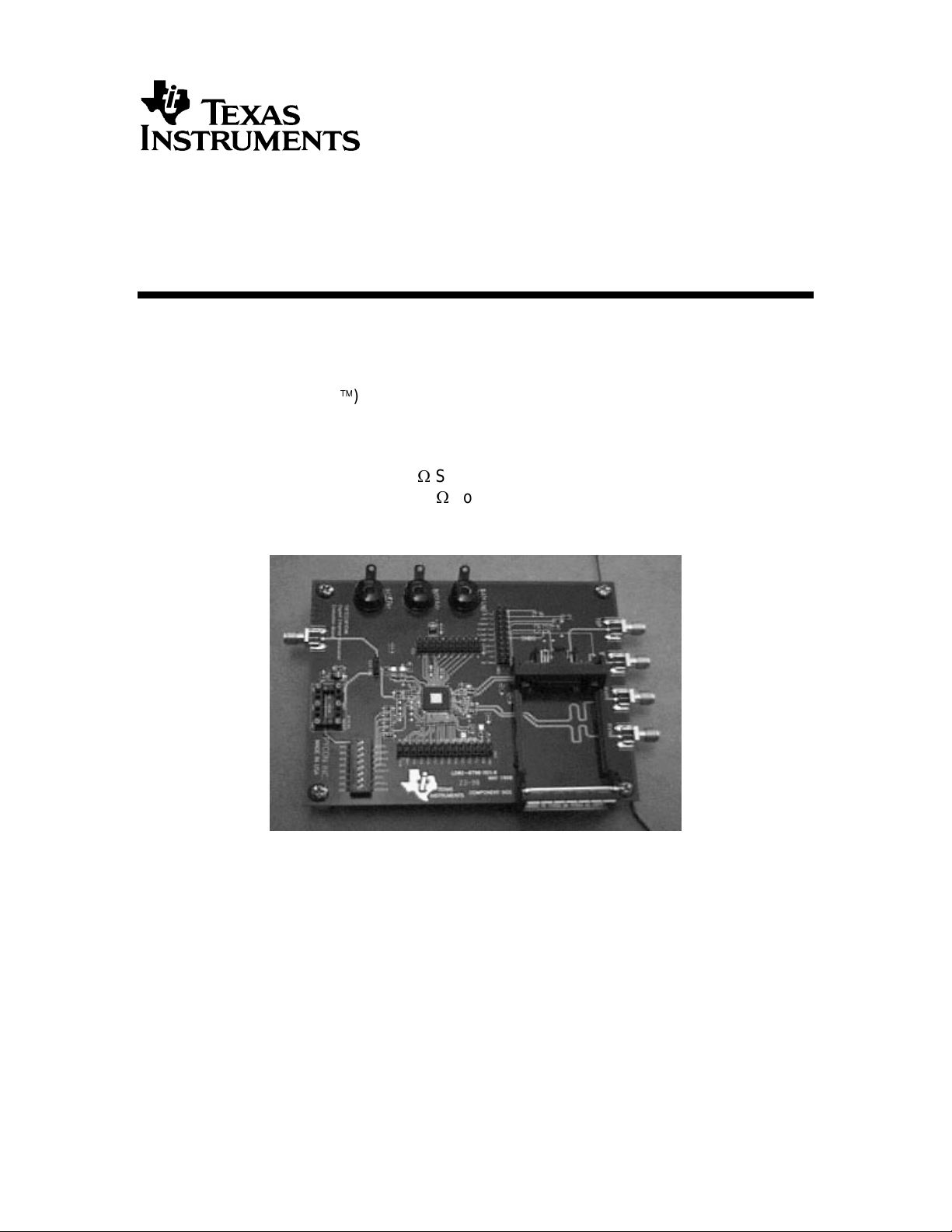
The Texas Instruments (TIä) TNETE2201 EVM (evaluation module) k it is a tool used to
evaluate and design high-speed prototypes using the TNETE2201 Ethernet Transceiver
IC (10 mm x 10 mm TQFP plastic package). The EVM kit is used to evaluate device
parameters while acting as a guide for high-speed board layout. The high-speed
interface is selectable between a 50-W SMA connector and a GBIC standard interface.
The GBIC standard also provides a 75-W copper interface module and various fiber optic
options. Overall, the designer can use the EVM kit as a tool for successful evaluation
and design of an end product.
Contents
Introduction......................................................................................................................................................2
Board Layout and Configuration......................................................................................................................3
Test Configuration and Results........................................................................................................................4
Board Layouts, Schematics, and Bill of Materials............................................................................................6
Digital Signal Processing Solutions March 1999
Page 2

Application Report
SLLA032
Figures
Figure 1. GBIC Setup Modifications................................................................................................................4
Figure 2. Bit Error-Rate Ratio Test Configuration ...........................................................................................5
Figure 3. Eye Diagrams of High-Speed Serial Outputs...................................................................................5
Figure 4. TNETE2201 EVM Board Schematic................................................................................................7
Figure 5. TNETE2201 EVM Board Top Layer.................................................................................................9
Figure 6. TNETE2201 EVM Board GND Layer.............................................................................................10
Figure 7. TNETE2201 EVM Board VCC Layer.............................................................................................11
Figure 8. TNETE2201 EVM Board Bottom Layer..........................................................................................12
Tables
Table 1. Default Setup as Shipped..................................................................................................................3
Table 2. TNETE2201 EVM Board Bill of Materials..........................................................................................8
Introduction
The TNETE2201 EVM kit can act as a daughter board that plugs into new or existing
designs. By providing the appropriate cabling, the EVM kit can interface with just about
any test equipment or other reference designs. The EVM kit's high-speed serial interface
can use either the GBIC (Gigabit Interface Converter) standard interface or a 50-ohm
SMA connection. In addition, the GBIC specification allows the designer to choose either
a 75-ohm copper module or a selection of fiber-optics modules.
As the frequency of operation increases, the board designer must take special care to
ensure that the highest signal integrity is maintained. To achieve this, the board’s
impedance is controlled for both 50-ohm and 75-ohm high-speed transmission lines. In
addition, the 50-ohm impedance mismatches are reduced by designing the component
pad size to be as close as possible to the width of the connecting transmission line. Vias
are minimized and, when necessary, placed as close as possible to the device drivers.
Overall, the board layout is designed and optimized to support high-speed operation.
Thus, understanding impedance control and transmission line effects are crucial when
designing high-speed boards.
Some of the advanced features offered by the EVM kit include:
r
PCB (printed circuit board) designed for speeds in excess of 1.25 Gbps
r
Flexible—The EVM can be configured to operate with multiple device types and with
copper or fiber interfaces.
r
Integrated GBIC Interface eliminates the need for two boards.
r
All input/output signals are accessible for rapid prototyping.
r
Clock input is selectable for either 8/14 pin crystal or external clock input.
r
Power can be supplied either by banana jacks or a 20-pin connector.
r
Series terminated parallel outputs
TNETE2201 EVM Kit Setup and Usage 2
Page 3

Application Report
SLLA032
Board Layout and Configurat ion
The TNETE2201 EVM kit is designed to give the developer many options for operation.
Many of these options are selectable by DIP switch and others may require board
component removal or additions. The following sections provide guidelines to config ure
the EVM kit for different modes of operation.
The EVM kit is normally delivered in a default configuration that requires external clock
and data inputs. The high-speed serial input and output are routed through the 50-ohm
transmission line path. The GBIC interface is not connected and would require some
resistor modifications to be functional. The default setup is useful for testing the board
and interface IC. The designer might consider testing the bit error rate, jitter, and eyediagram characteristics of the system. The TNETE2201 EVM is shipped with certain
components installed for default operation. Table 1 lists the default configuration.
Table 1. Default Setup as Shipped
Designator Function Condition (TNETE2201)
P5 CLK SEL Jumper installed between Pins 2 and 3
R1 TX Termination 200 ohm installed
R2 TX Termination 200 ohm installed
R5 Bias Net 365 ohm installed
R6 Bias Net 562 ohm installed
R8 WIZ OPTIO N Not installed
R9 WIZ OPTIO N Not installed
R16 CAP OPTION Zero ohm installed
R17 Bias Net Not installed
R21 WIZ OPTIO N Not installed
R22 WIZ OPTIO N Not installed
C13 Vcc Decouple 0.01 µF installed
C23 GBIC OPTION Not installed
C24 SMA OPTION 0.01 µF installed
C25 GBIC OPTION Not installed
C26 SMA OPTION 0.01 µF installed
C27 SMA OPTION 0.01 µF installed
C28 GBIC OPTION Not installed
C29 GBIC OPTION Not installed
C30 SMA OPTION 0.01 µF installed
C31 RX Termination 0.01 µF installed
C32 TX PLL Cap 0.0022 µF installed
C33 REF CLK Bias Net Zero 0hm installed
C34 TX PLL Cap 0.0022 µF installed
L1 Filter/Bias Ferrite installed
X1 OSC Not installed (not provided)
DIP1-1 PRBSEN X (OFF)
DIP1-2 TXRRAMP X (OFF)
DIP1-3 TXDIR X (OFF)
TNETE2201 EVM Kit Setup and Usage 3
Page 4
Application Report
SLLA032
Designator Function Condition (TNETE2201)
DIP1-4 LCKREFN X (OFF)
DIP1-5 TESTEN ON
DIP1-6 SYNCEN X (OFF)
DIP1-7 LOOPEN ON
DIP1-8 CLKEN X (OFF)
Note: X is a don't care state (default posi ti on).
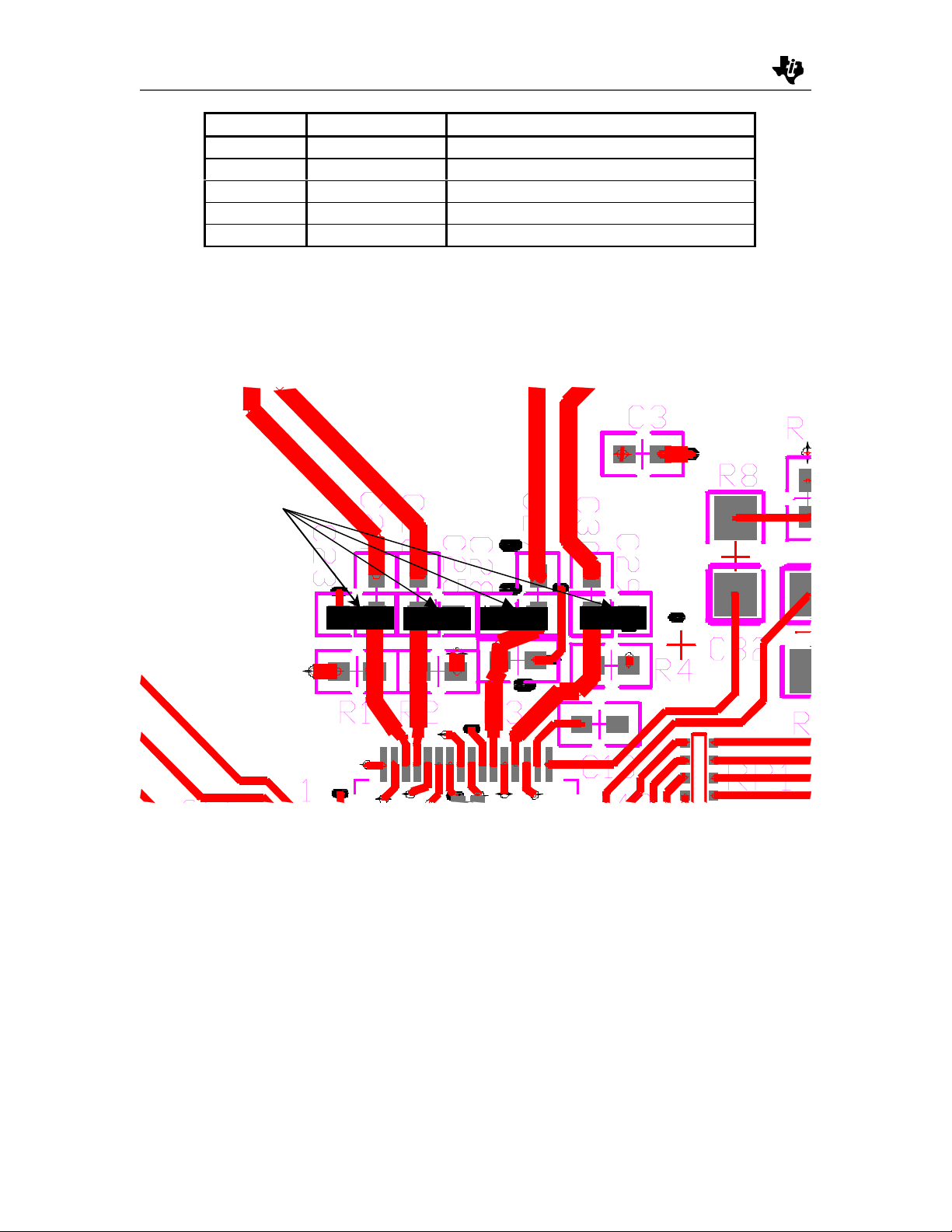
The GBIC Configuration requires a modification of the steering capacitors C23 through
C30. This requires removing C24, C26, C27, and C30 and soldering these capacitors in
locations C23, C25, C28, and C29 (see Figure 1).
Figure 1. GBIC Setup Modifications
GBIC
INSTALLED
CAPACITORS
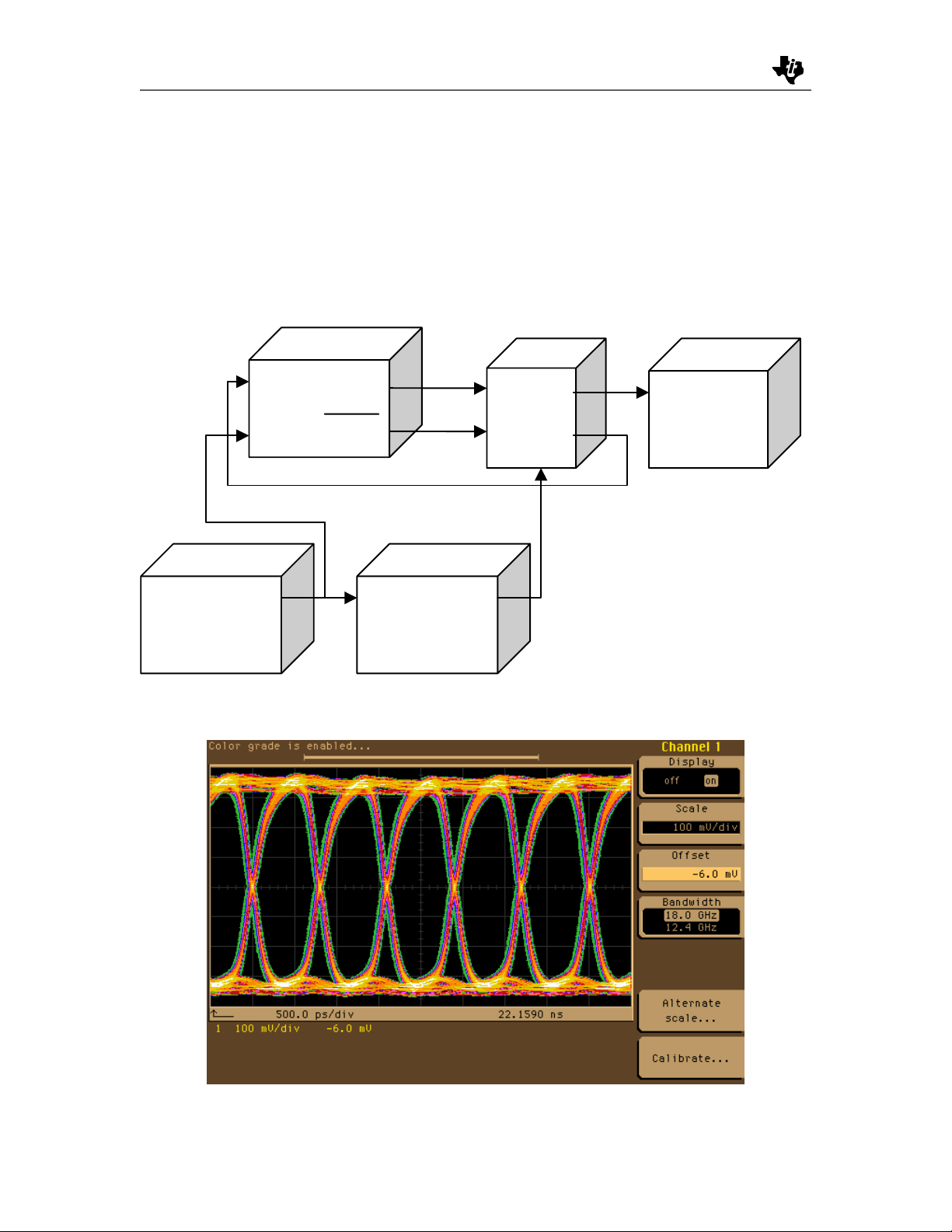
Test Configuration and Results
The serial Bit Error-rate Ratio Test (BERT) is useful for evaluating device and board
characteristics. Using this test, we can determine the eye diagram characteristics of the
system, as shown in Figure 3. The test setup is illustrated in Figure 2.
The HP71603B 3-Gbps Serial BERT outputs a high-speed serial stream to the test board
where the data is converted by the TNETE part to a 10-bit parallel format. The parallel
data is then looped back from the receiver to the transmitter. The pulse generator
provides a clock input to the transmitter. The external clock source is necessary because
the receiver's recovered clock is half the frequency necessary for transmission.
TNETE2201 EVM Kit Setup and Usage 4
Page 5
Application Report
SLLA032
Both the pulse generator and the BERT are synchronized with an external clock source.
The operator adjusts the variable phase delay to ensure that the clock meets the setup
and hold time of the data. The parallel data along with the clock is routed to the
transmitter where the data is serialized and captured by the oscilloscope. Figure 3 shows
an example eye diagram taken using this technique.
Figure 2. Bit Error-Rate Ratio Test Configuration
Wizard
(With parallel
ports looped)
RX-
RX+
External Clock
For Sync
Data In
Sync
HP71603B
BERT
Data Out
Data Out
Sync
(Variable Delay)
36”
36”
HP8133A
Pulse Generator
Clk Out
Figure 3. Eye Diagrams of High-Speed Serial Outputs
TX+
TX-
36”
REFCLK
HP54750A
Digital O’Scope
36”
Channel 1
TNETE2201 EVM Kit Setup and Usage 5
Page 6

Application Report
SLLA032
Board Layouts, Schematics, and Bill of Materials
TNETE2201 EVM Kit Setup and Usage 6
Page 7

Page 8

bom_list.txt
07/10/98 15:29:30 Electronics Design System Page: 0001
Bill of Materials
<<<From Job: fcge>>>
01-31xxx-xxx
TEXAS INSTRUMENTS INCORPORATED
Mixed Signal Products
T.I. Internal Data ENGINEER: RELEASED:________________
-----------------------------------------------------------------------------------------------------------------------------------ITEM| QTY | MFG | MFG PART# | Ref Des | DESCRIPTION | VALUE or FUNCTION | SOCKET
------------------------------------------------------------------------------------------------------------------------------------
1| 3 | PANASONIC | ECS-T1CX106R | C1,C35,C41 | CAPACITOR,TANT,SMT | 20%, 16V, 10uF |
2| 2 | AVX | 12061C222JATMA | C32,C34 | CAPACITOR,SMT1206 | 100V, 5%, 0.0022uF |
3| 35 | AVX | 06033G103JATMA | C2-C31,C36,C37 | CAPACITOR,SMT0603 | 25V,5%,0.01uF |
|* | | | C38-C40 | | |
4| 1 | AMP | 787653 | P4 | CONNECTOR,20PIN | RECEPT,R/A,20PIN,AMP |
5| 3 | CONCORD | 01-2520-3-044 | BJ(+5V) | CONNECTOR | BANANA,FEMALE,SWAGE MOUNT |
|* | | | BJ(RTN) | | |
|* | | | BJ(+3.3V) | | |
6| 5 | EFJOHNSON | 142-0701-801 | J1-J5 | CONNECTOR | SMA JACK,END LAUNCH,.062P |
7| 2 | MURATA ERIE | BLM21B03-PT | L1,L2 | FILTER,SMT0805 | FERRITE,6 OHMS@100MHz |
8| 2 | SAMTEC | TSW-110-07-G-D | P1,P6 | HEADER,2X10,.1CTRS | HEADER 2X 10 .1CTR |
9| 1 | SAMTEC | TSW-1-14-05-G-D | P2 | HEADER,MALE,2X14 | HEADER,MALE,2X14,.1CTRS |
10| 1 | ANY | HEADER,MALE,3PI | P5 | HEADER | MALE,3PIN,.100CC |
11| 1 | | DUT_PQFP_PJD64 | U1 | IC,TQFP,PJD,64PIN | DUT-USER DEFINED |
12| 3 | JUMPER | JUMPER-0603 | R16,R17 | JUMPER,SMT0603 | USER DEFINED JUMPER 0603 |
13| 1 | VARIES | OSC-COMBO-106.2 | X1 | OSCILLATOR,106.25MHz | OSC COMBO-106.25MHz | AMP/50935/X8
14| 4 | | RES1206(UN) | R8,R9,R21,R22 | RESISTOR,SMT,1206 | UN-INST |
15| 4 | AVX/KYOCERA | CRA3A4E500GI | RP1-RP4 | RES,SMT,8PIN,50OHM | SERIES CHIP RES ARRAY SMT |
16| 14 | DALE | CRCW06034701F | R7,R10-R14,R18 | RESISTOR,SMT,1/16W,1 | 4.70K OHM |
|* | | | R19,R23,R24 | | |
|* | | | R25-R28 | | |
17| 3 | DALE | CRCW060349R9F | R3,R4,R15 | RESISTOR,SMT,0603 | 49.9 OHM |
18| 2 | DALE | CRCW0603200F | R1,R2 | RESISTOR,SMT,0603 | 200 OHM |
19| 1 | DALE | CRCW0603365F | R5 | RESISTOR,SMT,0603 | 365 OHM |
20| 1 | DALE | CRCW0603562F | R6 | RESISTOR,SMT,0603 | 562 OHM |
21| 1 | C&K | BD08 | DIP1 | SWITCH,SPST,DIP16 | SWITCH,16P,SPST X 8 |
Total Part Count: 90
Total Parts Cost: 0
Page 1
Page 9

Page 10

Page 11

Page 12

Page 13

Application Report
SLLA032
TI Contact Numbers
INTERNET
TI Semiconductor Home Page
www.ti.com/sc
TI Distributors
www.ti.com/sc/docs/distmenu.htm
PRODUCT INFORMATION CENTERS
Americas
Phone +1(972) 644-5580
Fax +1(972) 480-7800
Email sc-infomaster@ti.com
Europe, Middle East, and Africa
Phone
Deutsch +49-(0) 8161 80 3311
English +44-(0) 1604 66 3399
Español +34-(0) 90 23 54 0 28
Francais +33-(0) 1-30 70 11 64
Italiano +33-(0) 1-30 70 11 67
Fax +44-(0) 1604 66 33 34
Email epic@ti.com
Japan
Phone
International +81-3-3457-0972
Domestic 0120-81-0026
Fax
International +81-3-3457-1259
Domestic 0120-81-0036
Email pic-japan@ti.com
Asia
Phone
International +886-2-23786800
Domestic
Australia 1-800-881-011
TI Number -800-800-1450
China 10810
TI Number -800-800-1450
Hong Kong 800-96-1111
TI Number -800-800-1450
India 000-117
TI Number -800-800-1450
Indonesia 001-801-10
TI Number -800-800-1450
Korea 080-551-2804
Malaysia 1-800-800-011
TI Number -800-800-1450
New Zealand 000-911
TI Number -800-800-1450
Philippines 105-11
TI Number -800-800-1450
Singapore 800-0111-111
TI Number -800-800-1450
Taiwan 080-006800
Thailand 0019-991-1111
TI Number -800-800-1450
Fax 886-2-2378-6808
Email tiasia@ti.com
TI is a trademark of Texas Instruments Incorporated.
Other brands and names are the property of their respective owners.
TNETE2201 EVM Kit Setup and Usage 13
Page 14

Application Report
SLLA032
Texas Instruments and its subsidiaries (TI) reserve the right to make changes to their
products or to discontinue any product or service without notice, and advise customers to
obtain the latest version of relevant information to verify, before placing orders, that
information being relied on is current and complete. All products are sold subject to the
terms and conditions of sale supplied at the time of order acknowledgement, including
those pertaining to warranty, patent infringement, and limitation of liability.
TI warrants performance of its semiconductor products to the specifications applicable at
the time of sale in accordance with TI's standard warranty. Testing and other quality
control techniques are utilized to the extent TI deems necessary to support this warranty.
Specific testing of all parameters of each device is not necessarily performed, except
those mandated by government requirements.
CERTAIN APPLICATIONS USING SEMICONDUCTOR PRODUCTS MAY INVOLVE
POTENTIAL RISKS OF DEATH, PERSONAL INJURY, OR SEVERE PROPERTY OR
ENVIRONMENTAL DAMAGE (“CRITICAL APPLICATIONS"). TI SEMICONDUCTOR
PRODUCTS ARE NOT DESIGNED, AUTHORIZED, OR WARRANTED TO BE
SUITABLE FOR USE IN LIFE-SUPPORT DEVICES OR SYSTEMS OR OTHER
CRITICAL APPLICATIONS. INCLUSION OF TI PRODUCTS IN SUCH APPLICATIONS
IS UNDERSTOOD TO BE FULLY AT THE CUSTOMER'S RISK.
IMPORTANT NOTICE
In order to minimize risks associated with the customer's applications, adequate design
and operating safeguards must be provided by the customer to minimize inherent or
procedural hazards.
TI assumes no liability for applications assistance or customer product design. TI does
not warrant or represent that any license, either express or implied, is granted under any
patent right, copyright, mask work right, or other intellectual property right of TI covering
or relating to any combination, machine, or process in which such semiconductor
products or services might be or are used. TI's publication of information regarding any
third party's products or services does not constitute TI's approval, warranty, or
endorsement thereof.
Copyright Ó 1999 Texas Instruments Incorporated
TNETE2201 EVM Kit Setup and Usage 14
 Loading...