

TMS418160A
1048576 BY 16-BIT
DYNAMIC RANDOM-ACCESS MEMORY
SMKS891C – AUGUST 1996 – REVISED OCTOBER 1997
1
POST OFFICE BOX 1443 • HOUSTON, TEXAS 77251–1443
This data sheet is applicable to TMS418160As
symbolized by Revision “E” and subsequent
revisions as described in the device
symbolization section.
D
Organization...1048576 by 16 Bits
D
Single 5-V Power Supply (± 10% T olerance)
D
1024-Cycle Refresh in 16 ms
D
Performance Ranges:
ACCESS ACCESS ACCESS READ/
TIME TIME TIME WRITE
t
RACtCAC
t
AA
CYCLE
MAX MAX MAX MIN
’418160A-50 50 ns 13 ns 25 ns 90 ns
’418160A-60 60 ns 15 ns 30 ns 110 ns
’418160A-70 70 ns 18 ns 35 ns 130 ns
D
Enhanced Page-Mode Operation With
xCAS
-Before-RAS (xCBR) Refresh
D
3-State Unlatched Output
D
Low Power Dissipation
D
High-Reliability Plastic 42-Lead
400-Mil-Wide Surface-Mount Small-Outline
J-Lead (SOJ) Package (DZ Suffix)
D
Ambient Temperature Range
0°C to 70°C
description
The TMS418160A is a 16777216-bit dynamic
random-access memory (DRAM) device organized as 1 048 576 words of 16 bits. It employs
state-of-the-art technology for high performance,
reliability, and low power at low cost.
This device features maximum RAS
access times
of 50-, 60-, and 70 ns. All address and data-in lines
are latched on chip to simplify system design.
Data out is unlatched to allow greater system
flexibility.
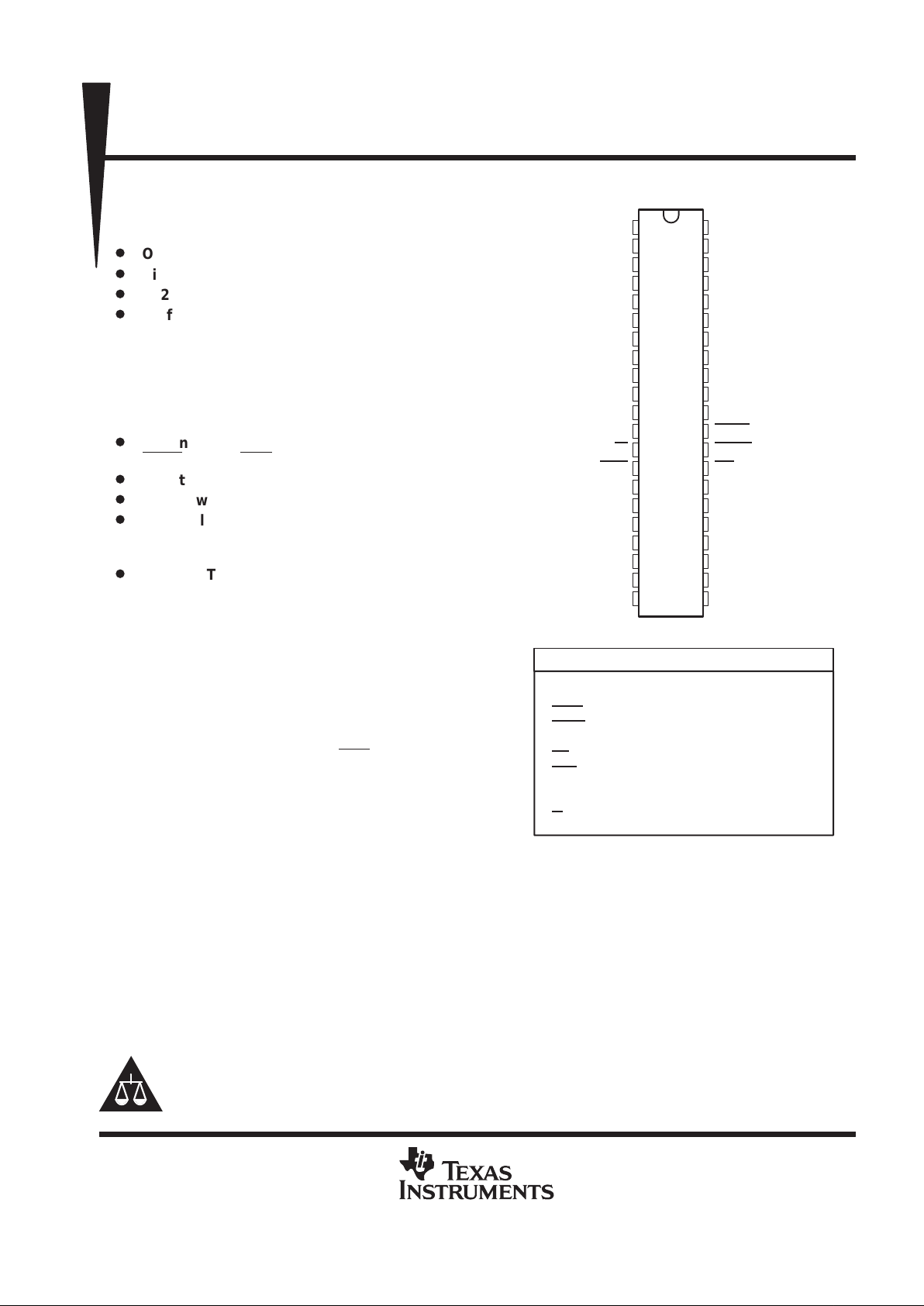
The TMS418160A is offered in a 42-lead plastic
surface-mount SOJ package (DZ suffix). This
package is designed for operation from 0° to 70°C.
Please be aware that an important notice concerning availability, standard warranty, and use in critical applications of
Texas Instruments semiconductor products and disclaimers thereto appears at the end of this data sheet.
PIN NOMENCLATURE
A[0:9] Address Inputs
DQ[0:15] Data In/Data Out
LCAS
Lower Column-Address Strobe
UCAS
Upper Column-Address Strobe
NC No Internal Connection
OE
Output Enable
RAS
Row-Address Strobe
V
DD
5-V Supply
V
SS
Ground
W
Write Enable
1
2
3
4
5
6
7
8
9
10
11
12
13
14
15
16
17
18
19
20
21
42
41
40
39
38
37
36
35
34
33
32
31
30
29
28
27
26
25
24
23
22
V
DD
DQ0
DQ1
DQ2
DQ3
V
DD
DQ4
DQ5
DQ6
DQ7
NC
NC
W
RAS
NC
NC
A0
A1
A2
A3
V
DD
V
SS
DQ15
DQ14
DQ13
DQ12
V
SS
DQ11
DQ10
DQ9
DQ8
NC
LCAS
UCAS
OE
A9
A8
A7
A6
A5
A4
V
SS
DZ PACKAGE
(TOP VIEW)
Copyright 1997, Texas Instruments Incorporated
PRODUCTION DATA information is current as of publication date.
Products conform to specifications per the terms of Texas Instruments
standard warranty. Production processing does not necessarily include
testing of all parameters.
TMS418160A
1048576 BY 16-BIT
DYNAMIC RANDOM-ACCESS MEMORY
SMKS891C – AUGUST 1996 – REVISED OCTOBER 1997
2
POST OFFICE BOX 1443 • HOUSTON, TEXAS 77251–1443
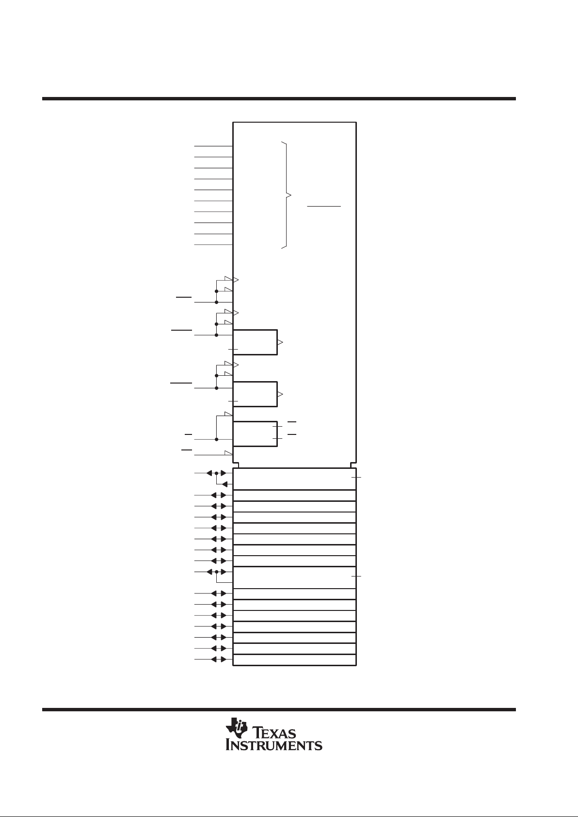
logic symbol
†
3
4
5
7
8
9
10
33
34
35
38
39
40
41
36
14
31
30
2
13
29
A0
A1
A2
A3
A4
A5
A6
A7
17
18
19
20
23
24
25
26
DQ1
DQ2
DQ3
DQ4
DQ5
DQ6
DQ7
DQ8
DQ9
DQ10
DQ11
DQ12
DQ13
DQ14
DQ15
DQ0
RAS
LCAS
UCAS
W
RAM 1M × 16
C20[ROW]
G23/[REFRESH ROW]
24[PWR DWN]
C21
G24
&
23C22
A,22D
A8
27
31
C21
G34
&
31
Z31
24,25EN27
34
,25EN37
23C32
23,21D
∇26,27
A, Z26
A,32D
∇36,37
A, Z36
OE
A
0
1 048 575
A9
28
25
20D19/21D9
20D10/21D0
†
This symbol is in accordance with ANSI/IEEE Std 91-1984 and IEC Publication 617-12.
TMS418160A
1048576 BY 16-BIT
DYNAMIC RANDOM-ACCESS MEMORY
SMKS891C – AUGUST 1996 – REVISED OCTOBER 1997
3
POST OFFICE BOX 1443 • HOUSTON, TEXAS 77251–1443
functional block diagram
A0
A1
A9
32
16
16
Timing and Control
Column-
Address
Buffers
Row-
Address
Buffers
I/O
Buffers
Data-
In
Reg.
Data-
Out
Reg.
Column Decode
Sense Amplifiers
R
o
w
D
e
c
o
d
e
256K Array
256K Array
256K Array
256K Array
256K Array
256K Array
DQ0–DQ15
RAS
UCAS W OELCAS
16 of 32
Selection
32
10
10
10
32
32
operation
dual xCAS
Two xCAS pins (LCAS and UCAS) are provided to give independent control of the 16 data I/O pins
(DQ0–DQ15), with LCAS
corresponding to DQ0–DQ7 and UCAS corresponding to DQ8–DQ15. Each xCAS
going low enables its corresponding DQx pin.
In write cycles, data-in setup and hold time (t
DS
and tDH) and write-command setup and hold time (t
WCS, tCWL
and t
WCH
) must be satisfied for each individual xCAS to ensure writing into the storage cells of the corresponding
DQ pins.
Different modes of operation for upper and lower bytes in one cycle are not allowed, such as the example shown
in Figure 1.
RAS
UCAS
LCAS
W
Delayed write
Early write
Figure 1. Illegal Dual-xCAS Operation

TMS418160A
1048576 BY 16-BIT
DYNAMIC RANDOM-ACCESS MEMORY
SMKS891C – AUGUST 1996 – REVISED OCTOBER 1997
4
POST OFFICE BOX 1443 • HOUSTON, TEXAS 77251–1443
enhanced page mode
Page-mode operation allows faster memory access by keeping the same row address while selecting random
column addresses. The time for row-address setup and hold and address multiplexing is eliminated. The
maximum number of columns that can be accessed is determined by the maximum RAS
low time and the xCAS
page-mode cycle time used. With minimum xCAS page-cycle time, all columns can be accessed without
intervening RAS
cycles.
Unlike conventional page-mode DRAMs, the column-address buffers in this device are activated on the falling
edge of RAS
. The buffers act as transparent or flow-through latches while xCAS is high. The falling edge of the
first xCAS
latches the column addresses. This performance improvement is referred to as enhanced-page
mode. This feature allows the devices to operate at a higher data bandwidth than conventional page-mode
because data retrieval begins as soon as the column address is valid rather than when xCAS
transitions low.
A valid column address may be presented immediately after t
RAH
(row-address hold time) has been satisfied,
usually well in advance of the falling edge of xCAS
. In this case, data is obtained after t
CAC
maximum (access
time from xCAS
low) if tAA maximum (access time from column address) has been satisfied. In the event that
column addresses for the next page cycle are valid at the time xCAS
goes high, minimum access time for the
next cycle is determined by t
CPA
.
address: A0–A9
Twenty address bits are required to decode each of the 1048576 storage cell locations. Twelve row-address
bits are set up on A0 through A1 1 and latched onto the chip by RAS
. Eight column-address bits are set up on
A0 through A7 and latched onto the chip by the first xCAS
. All addresses must be stable on or before the falling
edge of RAS
and xCAS. RAS is similar to a chip enable in that it activates the sense amplifiers as well as the
row decoder. xCAS
is used as a chip select, activating its corresponding output buffer and latching the address
bits into the column-address buffers.
The column address is latched on the first xCAS
falling edge with address setup and hold parameters
referenced to that edge. In order to latch in a new column address, both xCAS
pins must be brought high. The
column-precharge time (see parameter t
CP
) is measured from the last xCAS rising edge to the first xCAS falling
edge of the new cycle. Keeping a column address valid while toggling xCAS
requires a minimum hold time,
t
CLCH
. During t
CLCH
, at least one xCAS must be brought low before the other xCAS is taken high.
write enable (W
)
Read- or write mode is selected through W
. A logic high on W selects the read mode and a logic low selects
the write mode. Data in is disabled when the read mode is selected. When W
goes low prior to xCAS (early write),
data out remains in the high-impedance state for the entire cycle, permitting a write operation independent of
the state of OE
. This permits early-write operations to be completed with OE grounded.
data in (DQ0–DQ15)
Data is written during a write- or read-modify-write cycle. Depending on the mode of operation, the falling edge
of xCAS
or W strobes data into the on-chip data latch. In an early-write cycle, W is brought low prior to a xCAS
falling edge and the data is strobed into the on-chip data latch for the corresponding DQs with setup-and-hold
times referenced to this xCAS
signal.
In a delayed-write- or read-modify-write cycle, xCAS
is already low and the data is strobed in by W with setup
and hold times referenced to this signal. Also, OE
must be high to bring the output buffers to the high-impedance
state prior to impressing data on the I/O lines (see parameter t
OED
).

TMS418160A
1048576 BY 16-BIT
DYNAMIC RANDOM-ACCESS MEMORY
SMKS891C – AUGUST 1996 – REVISED OCTOBER 1997
5
POST OFFICE BOX 1443 • HOUSTON, TEXAS 77251–1443
data out (DQ0–DQ15)
Data out is the same polarity as data in. The output is in the high-impedance (floating) state until xCAS
and OE
are brought low. In a read cycle, the output becomes valid after the access-time-interval t
CAC
(which begins with
the negative transition of xCAS
) as long as t
RAC
(access time from RAS) and tAA (access time from column
address) are satisfied. The delay time from xCAS
low to valid data out is measured from each individual xCAS
to its corresponding DQx pin.
output enable (OE
)
OE
controls the impedance of the output buffers. When OE is high, the buffers remain in the high-impedance
state. Bringing OE
low during a normal cycle activates the output buffers, putting them in the low-impedance
state. It is necessary for both RAS
and xCAS to be brought low (until either OE or xCAS is brought high) for the
output buffers to go into the low-impedance state.
RAS
-only refresh
A refresh operation must be performed once every 16 ms to retain data. This can be achieved by strobing each
of the 1024 rows (A0–A9). A normal read or write cycle refreshes all bits in each row that is selected. A RAS
-only
operation can be used by holding both xCAS
at the high (inactive) level, conserving power as the output buffers
remain in the high-impedance state. Externally generated addresses must be used for a RAS
-only refresh.
hidden refresh
Hidden refresh can be performed while maintaining valid data at the output pin. This is accomplished by holding
xCAS
at VIL after a read operation and cycling RAS after a specified precharge period, similar to a RAS-only
refresh cycle. The external address is ignored, and the refresh address is generated internally.
xCAS-before-RAS (xCBR) refresh
xCBR refresh is utilized by bringing at least one xCAS
low earlier than RAS (see parameter t
CSR
) and holding
it low after RAS
falls (see parameter t
CHR
). For successive xCBR refresh cycles, xCAS can remain low while
cycling RAS
. The external address is ignored and the refresh address is generated internally.
power up
To achieve proper device operation, an initial pause of 200 µs, followed by a minimum of eight initialization
cycles, is required after power up to the full V
DD
level. These eight initialization cycles must include at least one
refresh (RAS
-only or xCBR) cycle.
TMS418160A
1048576 BY 16-BIT
DYNAMIC RANDOM-ACCESS MEMORY
SMKS891C – AUGUST 1996 – REVISED OCTOBER 1997
6
POST OFFICE BOX 1443 • HOUSTON, TEXAS 77251–1443
absolute maximum ratings over ambient temperature range (unless otherwise noted)
†
Supply voltage range, V
DD
– 1 V to 7 V. . . . . . . . . . . . . . . . . . . . . . . . . . . . . . . . . . . . . . . . . . . . . . . . . . . . . . . . . . . .
Voltage range on any pin (see Note 1) – 1 V to 7 V. . . . . . . . . . . . . . . . . . . . . . . . . . . . . . . . . . . . . . . . . . . . . . . . . .
Short-circuit output current 50 mA. . . . . . . . . . . . . . . . . . . . . . . . . . . . . . . . . . . . . . . . . . . . . . . . . . . . . . . . . . . . . . . .
Power dissipation 1 W. . . . . . . . . . . . . . . . . . . . . . . . . . . . . . . . . . . . . . . . . . . . . . . . . . . . . . . . . . . . . . . . . . . . . . . . . .
Ambient temperature range, T
A
0°C to 70°C. . . . . . . . . . . . . . . . . . . . . . . . . . . . . . . . . . . . . . . . . . . . . . . . . . . . . . .
Storage temperature range, T
stg
–55°C to 125°C. . . . . . . . . . . . . . . . . . . . . . . . . . . . . . . . . . . . . . . . . . . . . . . . . .
†
Stresses beyond those listed under “absolute maximum ratings” may cause permanent damage to the device. These are stress ratings only, and
functional operation of the device at these or any other conditions beyond those indicated under “recommended operating conditions” is not
implied. Exposure to absolute-maximum-rated conditions for extended periods may affect device reliability.
NOTE 1: All voltage values are with respect to VSS.
recommended operating conditions
MIN NOM MAX UNIT
V
DD
Supply voltage 4.5 5 5.5 V
V
SS
Supply voltage 0 V
V
IH
High-level input voltage 2.4 6.5 V
V
IL
Low-level input voltage (see Note 2) –1 0.8 V
T
A
Ambient temperature 0 70
°C
NOTE 2: The algebraic convention, where the more negative (less positive) limit is designated as minimum, is used for logic-voltage levels only.
TMS418160A
1048576 BY 16-BIT
DYNAMIC RANDOM-ACCESS MEMORY
SMKS891C – AUGUST 1996 – REVISED OCTOBER 1997
7
POST OFFICE BOX 1443 • HOUSTON, TEXAS 77251–1443
electrical characteristics over recommended ranges of supply voltage and ambient temperature
(unless otherwise noted)
’418160A-50 ’418160A-60 ’418160A- 70
PARAMETER
TEST CONDITIONS
†
MIN MAX MIN MAX MIN MAX
UNIT
V
OH
High-level output
voltage
IOH = – 5 mA 2.4 2.4 2.4 V
V
OL
Low-level output voltage IOL = 4.2 mA 0.4 0.4 0.4 V
I
I
Input current (leakage)
VDD = 5.5 V, VI = 0 V to 6.5 V,
All others = 0 V to V
DD
± 10 ± 10 ± 10 µA
I
O
Output current (leakage)
VDD = 5.5 V, VO = 0 V to VDD,
xCAS
high
± 10 ± 10 ± 10 µA
I
CC1
‡§
Average read- or
write-cycle current
VDD = 5.5 V, Minimum cycle 180 160 150 mA
VIH = 2.4 V (TTL),
After one memory cycle,
RAS
and xCAS high
2 2 2 mA
I
CC2
Average standby current
VIH = VDD – 0.2 V (CMOS),
After one memory cycle,
RAS
and xCAS high
1 1 1 mA
I
CC3
§
Average refresh current
(RAS
-only refresh or
xCBR)
VDD = 5.5 V, Minimum cycle,
RAS
cycling, xCAS high
(RAS
only),
RAS
low after xCAS low (xCBR)
180 160 150 mA
I
CC4
‡¶
Average page current
VDD = 5.5 V, tPC = MIN,
RAS
low, xCAS cycling
110 90 80 mA
†
For conditions shown as MIN/MAX, use the appropriate value specified in the timing requirements.
‡
Measured with outputs open
§
Measured with a maximum of one address change while RAS
= V
IL
¶
Measured with a maximum of one address change during each page cycle, t
PC
capacitance over recommended ranges of supply voltage and ambient temperature,
f = 1 MHz (see Note 3)
PARAMETER MIN MAX UNIT
C
i(A)
Input capacitance, A0–A9 5 pF
C
i(OE)
Input capacitance, OE 7 pF
C
i(RC)
Input capacitance, xCAS and RAS 7 pF
C
i(W)
Input capacitance, W 7 pF
C
O
Output capacitance
#
7 pF
#
LCAS
and UCAS = VIH to disable outputs
NOTE 3: VDD = 5 V
± 10%, and the bias on pins under test is 0 V .
TMS418160A
1048576 BY 16-BIT
DYNAMIC RANDOM-ACCESS MEMORY
SMKS891C – AUGUST 1996 – REVISED OCTOBER 1997
8
POST OFFICE BOX 1443 • HOUSTON, TEXAS 77251–1443
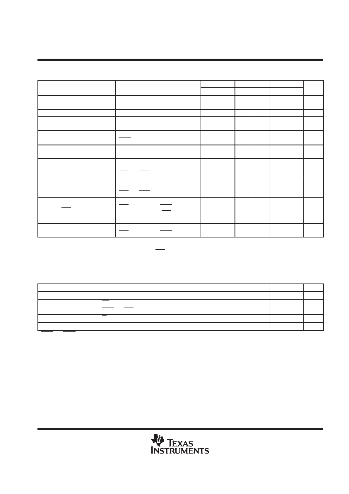
switching characteristics over recommended ranges of supply voltage and ambient temperature
(see Note 4)
’418160A-50 ’418160A-60 ’418160A-70
PARAMETER
MIN MAX MIN MAX MIN MAX
UNIT
t
AA
Access time from column address 25 30 35 ns
t
CAC
Access time from xCAS 13 15 18 ns
t
CPA
Access time from xCAS precharge 30 35 40 ns
t
RAC
Access time from RAS 50 60 70 ns
t
OEA
Access time from OE 13 15 18 ns
t
CLZ
Delay time, xCAS to output in the low-impedance state 0 0 0 ns
t
OH
Output data hold time from xCAS 3 3 3 ns
t
OHO
Output data hold time from OE 3 3 3 ns
t
OFF
Output buffer turn-off delay from xCAS (see Note 5) 0 13 0 15 0 18 ns
t
OEZ
Output buffer turn-off delay from OE (see Note 5) 0 13 0 15 0 18 ns
NOTES: 4. With ac parameters, it is assumed that tT = 5 ns.
5. t
OFF
and t
OEZ
are specified when the output is no longer driven. Data-in should not be enabled until one of the applicable maximum
specifications is satsified.
ac timing requirements (see Note 4)
’418160A-50 ’418160A-60 ’418160A-70
MIN MAX MIN MAX MIN MAX
UNIT
t
RC
Cycle time, read 90 110 130 ns
t
WC
Cycle time, write 90 110 130 ns
t
RWC
Cycle time, read-write 131 155 181 ns
t
PC
Cycle time, page-mode read or write (see Note 6) 35 40 45 ns
t
PRWC
Cycle time, page-mode read-write 76 85 96 ns
t
RASP
Pulse duration, RAS active, page mode (see Note 7) 50 100 000 60 100000 70 100000 ns
t
RAS
Pulse duration, RAS active, nonpage mode (see Note 7) 50 10 000 60 10 000 70 10 000 ns
t
CAS
Pulse duration, xCAS active (see Note 8) 13 10 000 15 10 000 18 10 000 ns
t
RP
Pulse duration, RAS (precharge) 30 40 50 ns
t
WP
Pulse duration, write command 10 10 10 ns
t
ASC
Setup time, column address 0 0 0 ns
t
ASR
Setup time, row address 0 0 0 ns
t
DS
Setup time, data-in (see Note 9) 0 0 0 ns
t
RCS
Setup time, read command 0 0 0 ns
t
CWL
Setup time, write command before xCAS precharge 13 15 18 ns
t
RWL
Setup time, write command before RAS precharge 13 15 18 ns
t
WCS
Setup time, write command before xCAS active
(early-write only)
0 0 0 ns
t
WRP
Setup time, write before RAS active (CBR refresh only) 10 10 10 ns
NOTES: 4. With ac parameters, it is assumed that tT = 5 ns.
6. To assure tPC min, t
ASC
should be ≥ to tCP.
7. In a read-write cycle, t
RWD
and t
RWL
must be observed.
8. In a read-write cycle, t
CWD
and t
CWL
must be observed.
9. Referenced to the later of xCAS
or W in write operations

TMS418160A
1048576 BY 16-BIT
DYNAMIC RANDOM-ACCESS MEMORY
SMKS891C – AUGUST 1996 – REVISED OCTOBER 1997
9
POST OFFICE BOX 1443 • HOUSTON, TEXAS 77251–1443
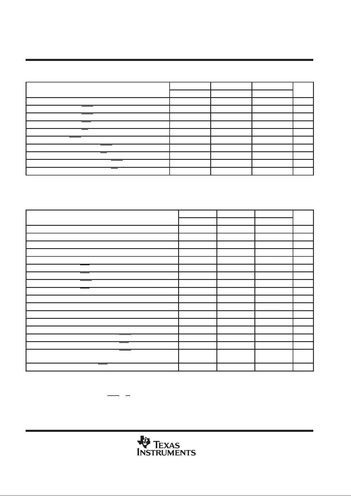
ac timing requirements (see Note 4) (continued)
’418160A-50 ’418160A - 60 ’418160A-70
MIN MAX MIN MAX MIN MAX
UNIT
t
CAH
Hold time, column address 10 10 15 ns
t
DH
Hold time, data-in (see Note 9) 10 10 15 ns
t
RAH
Hold time, row address 8 10 10 ns
t
RCH
Hold time, read command referenced to xCAS (see Note 10) 0 0 0 ns
t
RRH
Hold time, read command referenced to RAS (see Note 10) 0 0 0 ns
t
WCH
Hold time, write command during xCAS active
(early-write only)
10 10 15 ns
t
CLCH
Hold time, xCAS low to xCAS high 5 5 5 ns
t
RHCP
Hold time, RAS active from xCAS precharge 30 35 40 ns
t
OEH
Hold time, OE command 13 15 18 ns
t
ROH
Hold time, RAS referenced to OE 10 10 10 ns
t
WRH
Hold time, write after RAS active (CBR refresh only) 10 10 10 ns
t
CP
Delay time, xCAS precharge 8 10 10 ns
t
AWD
Delay time, column address to write command
(read-write operation only)
48 55 63 ns
t
CHR
Delay time, xCAS referenced to RAS (xCBR refresh only) 10 10 10 ns
t
CRP
Delay time, xCAS precharge to RAS 5 5 5 ns
t
CSH
Delay time, RAS active to xCAS precharge 50 60 70 ns
t
CSR
Setup time, xCAS referenced to RAS (xCBR refresh only) 5 5 5 ns
t
CWD
Delay time, xCAS to write command (read-write operation only) 36 40 46 ns
t
OED
Delay time, OE to data in 13 15 18 ns
t
RAD
Delay time, RAS to column address (see Note 11) 13 25 15 30 15 35 ns
t
RAL
Delay time, column address to RAS precharge 25 30 35 ns
t
CAL
Delay time, column address to xCAS precharge 25 30 35 ns
t
RCD
Delay time, RAS to xCAS (see Note 11) 18 37 20 45 20 52 ns
t
RPC
Delay time, RAS precharge to xCAS active 5 5 5 ns
t
RSH
Delay time, xCAS active to RAS precharge 13 15 18 ns
t
RWD
Delay time, RAS to write command (read-write operation only) 73 85 98 ns
t
CPW
Delay time, xCAS precharge to write command
(read-write operation only)
53 60 68 ns
t
REF
Refresh time interval 16 16 16 ms
t
T
Transition time 2 30 2 30 2 30 ns
NOTES: 4. With ac parameters, it is assumed that tT = 5 ns.
9. Referenced to the later of xCAS
or W in write operations
10. Either t
RRH
or t
RCH
must be satisfied for a read cycle.
11. The maximum value is specified only to assure access time.

TMS418160A
1048576 BY 16-BIT
DYNAMIC RANDOM-ACCESS MEMORY
SMKS891C – AUGUST 1996 – REVISED OCTOBER 1997
10
POST OFFICE BOX 1443 • HOUSTON, TEXAS 77251–1443
PARAMETER MEASUREMENT INFORMATION
V
TH
R
L
Output Under Test
CL = 100 pF
(a) LOAD CIRCUIT
V
DD
R1
Output Under Test
(b) ALTERNATE LOAD CIRCUIT
R2
CL = 100 pF
NOTE A: CL includes probe and fixture capacitance.
(see Note A)
(see Note A)
DEVICE
VDD (V) R1 (Ω) R2 (Ω) VTH (V) RL (Ω)
’418160A 5 828 295 1.31 218
Figure 2. Load Circuits for Timing Parameters

TMS418160A
1048576 BY 16-BIT
DYNAMIC RANDOM-ACCESS MEMORY
SMKS891C – AUGUST 1996 – REVISED OCTOBER 1997
11
POST OFFICE BOX 1443 • HOUSTON, TEXAS 77251–1443
PARAMETER MEASUREMENT INFORMATION
(see Note B)
RAS
UCAS
LCAS
Address
W
DQ0–DQ15
OE
Row Column
t
CAS
t
RC
t
RAS
t
T
t
RCD
t
RP
t
CP
t
CRP
t
RSH
t
RAD
t
RAH
t
ASC
t
RAL
t
CAH
t
RRH
t
CAC
t
AA
t
RAC
t
OEA
t
ROH
t
OEZ
Don’t Care
t
RCS
t
ASR
Don’t Care
Don’t Care
t
RCH
t
OFF
Valid Data Out
t
CLZ
t
CLCH
(see Note A)
t
OH
Don’t Care Don’t Care
t
OHO
t
CSH
t
CAL
See Note C
t
CAS
NOTES: A. To hold the address latched by the first xCAS going low, the parameter t
CLCH
must be met.
B. t
CAC
is measured from xCAS
to its corresponding DQx.
C. Output can go from the high-impedance state to an invalid-data state prior to the specified access time.
D. xCAS
order is arbitrary.
Figure 3. Read-Cycle Timing

TMS418160A
1048576 BY 16-BIT
DYNAMIC RANDOM-ACCESS MEMORY
SMKS891C – AUGUST 1996 – REVISED OCTOBER 1997
12
POST OFFICE BOX 1443 • HOUSTON, TEXAS 77251–1443
PARAMETER MEASUREMENT INFORMATION
RAS
UCAS
LCAS
Address
W
DQ0–DQ15
OE
Row Column Don’t Care
Valid Data In
t
WC
t
RAS
t
RP
t
CAS
t
RCD
t
T
t
CP
t
CRP
t
RSH
t
RAH
t
ASC
t
CAL
t
RAL
t
RAD
t
CAH
t
CWL
t
RWL
t
WP
t
DH
t
OED
t
OEH
t
DS
t
CLCH
Don’t Care
Don’t Care
t
ASR
(see Note A)
Don’t Care
Don’t CareDon’t Care
t
CSH
(see Note C)
NOTES: A. To hold the address latched by the first xCAS going low, the parameter t
CLCH
must be met.
B. xCAS
order is arbitrary.
C. t
CWL
must be satisfied for each xCAS
to write properly to each byte.
Figure 4. Write-Cycle Timing

TMS418160A
1048576 BY 16-BIT
DYNAMIC RANDOM-ACCESS MEMORY
SMKS891C – AUGUST 1996 – REVISED OCTOBER 1997
13
POST OFFICE BOX 1443 • HOUSTON, TEXAS 77251–1443
PARAMETER MEASUREMENT INFORMATION
RAS
UCAS
LCAS
Address
W
DQ8–DQ15
OE
t
WC
t
RAS
t
T
t
RCD
t
CRP
t
RP
t
CP
t
ASR
t
RAD
t
RAH
t
ASC
t
WCS
t
WP
t
DS
Valid Data In
Row
Column
Don’t Care
Don’t Care
t
CAS
t
RSH
Don’t Care
t
CWL
t
CLCH
(see Note A)
Don’t Care
DQ0–DQ7
t
DH
t
DS
Valid Data In
Don’t Care
t
CSH
t
CAL
t
RAL
t
DH
t
RWL
t
CAH
t
WCH
t
WCS
(see Note C)
(see Note C)
t
WCH
(see Note C)
Don’t Care
Don’t Care
Don’t Care
(see Note D)
(see Note D)
(see Note D)
(See Note C)
(see Note E)
t
CAS
See Note E
NOTES: A. To hold the address latched by the first xCAS going low, the parameter t
CLCH
must be met.
B. xCAS
order is arbitrary.
C. t
WCS
and t
WCH
must be satisfied for each xCAS
.
D. tDS and tDH of a DQ input are referenced to the corresponding xCAS
.
E. t
CWL
must be satisfied for each xCAS
to write properly to each byte.
Figure 5. Early-Write-Cycle Timing

TMS418160A
1048576 BY 16-BIT
DYNAMIC RANDOM-ACCESS MEMORY
SMKS891C – AUGUST 1996 – REVISED OCTOBER 1997
14
POST OFFICE BOX 1443 • HOUSTON, TEXAS 77251–1443
PARAMETER MEASUREMENT INFORMATION
RAS
xCAS
Address
W
OE
DQ0–DQ15
t
RWC
Row Column
Don’t Care
Don’t Care
Don’t Care
Data
Out
Don’t Care
Don’t Care
Data
In
t
RAS
t
RCD
t
T
t
CAS
t
RP
t
CRP
t
CP
t
T
t
CAH
t
ASC
t
RAH
t
ASR
t
RAD
t
RCS
t
RWD
t
RWL
t
WP
t
AWD
t
CWD
t
CAC
t
DS
t
DH
t
AA
t
CLZ
t
RAC
t
OEA
t
OEZ
t
OEH
See Note A
t
CWL
t
OHO
t
OED
NOTE A: Output can go from high-impedance state to an invalid-data state prior to the specified access time.
Figure 6. Read-Write-Cycle Timing

TMS418160A
1048576 BY 16-BIT
DYNAMIC RANDOM-ACCESS MEMORY
SMKS891C – AUGUST 1996 – REVISED OCTOBER 1997
15
POST OFFICE BOX 1443 • HOUSTON, TEXAS 77251–1443
PARAMETER MEASUREMENT INFORMATION
Don’t
Care
Don’t Care
Valid
Out
Valid
Out
Valid
Out
RAS
UCAS
Address
W
DQ8–DQ15
DQ0–DQ7
OE
Column Column
t
RASP
t
RCD
t
CRP
t
RP
t
RSH
t
PC
t
CP
t
ASR
t
RAH
t
ASC
t
CAH
t
CAL
t
RAL
t
RAD
t
RCH
t
RRH
t
OHO
t
OEZ
t
RCS
t
AA
t
RAC
t
AA
t
OEA
LCAS
Row
Don’t Care
t
CAC
Don’t
Care
t
CPA
t
CSH
t
CAS
t
CLZ
t
RHCP
(see Note C)
t
OH
See Note D
See Note D
t
OHO
t
OEA
t
OFF
Don’t CareDon’t Care
(see Note B)
t
CLCH
(see Note A)
t
CAS
NOTES: A. To hold the address latched by the first xCAS going low, the parameter t
CLCH
must be met.
B. t
CAC
is measured from xCAS
to its corresponding DQx.
C. Access time is t
CPA
-, tAA-, or t
CAC
-dependent.
D. Output can go from the high-impedance state to an invalid-data state prior to the specified access time.
E. A write cycle or read-modify-write cycle can be mixed with the read cycles as long as the write- and read-modify-write timing
specifications are not violated.
F. xCAS
order is arbitrary.
Figure 7. Enhanced-Page-Mode Read-Cycle Timing

TMS418160A
1048576 BY 16-BIT
DYNAMIC RANDOM-ACCESS MEMORY
SMKS891C – AUGUST 1996 – REVISED OCTOBER 1997
16
POST OFFICE BOX 1443 • HOUSTON, TEXAS 77251–1443
PARAMETER MEASUREMENT INFORMATION
RAS
UCAS
LCAS
Address
W
DQ8–
DQ15
DQ0–
DQ7
OE
t
RASP
t
RP
t
RSH
t
CRP
t
PC
t
CSH
t
RCD
t
CAS
t
CP
t
CAL
t
RAL
t
CAH
t
ASR
t
RAH
t
RAD
t
CWL
t
WP
t
CWL
t
RWL
t
DH
t
DS
t
OED
Don’t Care
Don’t Care Don’t Care Don’t Care
Don’t Care
Column Column
Valid In
Valid In
Valid In
Row
t
CLCH
t
ASC
t
RHCP
(see Note A)
Don’t Care
Don’t Care
t
DS
t
DH
(see Note D)
t
CAS
NOTES: A. To hold the address latched by the first xCAS going low, the parameter t
CLCH
must be met.
B. A read cycle or read-modify-write cycle can be mixed with the write cycles as long as the read- and read-modify-write timing
specifications are not violated.
C. xCAS
order is arbitrary.
D. t
CWL
must be satisfied for each xCAS
to ensure proper writing to each byte.
Figure 8. Enhanced-Page-Mode Write-Cycle Timing

TMS418160A
1048576 BY 16-BIT
DYNAMIC RANDOM-ACCESS MEMORY
SMKS891C – AUGUST 1996 – REVISED OCTOBER 1997
17
POST OFFICE BOX 1443 • HOUSTON, TEXAS 77251–1443
PARAMETER MEASUREMENT INFORMATION
RAS
UCAS
LCAS
Address
W
DQ8–
DQ15
DQ0–
DQ7
OE
t
RASP
t
RP
t
RSH
t
CRP
t
PC
t
CSH
t
RCD
t
CAS
t
CP
t
CAL
t
RAL
t
CAH
t
ASR
t
RAH
t
RAD
t
CWL
t
CWL
t
RWL
t
DH
t
DS
Don’t Care
Don’t Care Don’t Care Don’t Care
Don’t Care
Column Column
Valid In
Valid In
Valid In
Row
t
CLCH
t
ASC
t
WCH
t
RHCP
(see Note A)
Don’t Care
Don’t Care
t
WCS
(see Note D)
(see Note D)
(see Note E)
(see Note E)
(see Note F)
t
CAS
NOTES: A. To hold the address latched by the first xCAS
going low, the parameter t
CLCH
must be met.
B. A read cycle or read-modify-write cycle can be mixed with the write cycles as long as the read- and read-modify-write timing
specifications are not violated.
C. xCAS
order is arbitrary.
D. t
WCS
and t
WCH
must be satisfied for each xCAS
.
E. tDS and tDH for a DQ is referenced to the corresponding xCAS
.
F. t
CWL
must be satisfied for each xCAS
.
Figure 9. Enhanced-Page-Mode Early Write-Cycle Timing

TMS418160A
1048576 BY 16-BIT
DYNAMIC RANDOM-ACCESS MEMORY
SMKS891C – AUGUST 1996 – REVISED OCTOBER 1997
18
POST OFFICE BOX 1443 • HOUSTON, TEXAS 77251–1443
PARAMETER MEASUREMENT INFORMATION
RAS
UCAS
Address
W
OE
Column
t
RASP
ColumnRow
Valid Out
Valid In Valid In
Valid Out
t
RP
t
CRP
t
RSH
t
CP
t
CSH
t
PRWC
t
CAS
t
RCD
t
ASR
t
ASC
t
CAH
t
CWD
t
AWD
t
RWD
t
CWL
t
RWL
t
RAH
t
CAC
t
CPA
t
OEH
t
OED
t
OEH
t
OEZ
t
OEA
t
AA
t
RAC
t
RCS
(see Note C)
t
DS
t
CLZ
LCAS
t
CLCH
t
RAD
DQ0–DQ15
(see Note A)
t
WP
t
AA
t
DH
(see Note B)
t
CPW
t
CAS
NOTES: A. To hold the address latched by the first xCAS going low, the parameter t
CLCH
must be met.
B. Access time is t
CPA
-, tAA-, or t
CAC
-dependent.
C. Output can go from the high-impedance state to an invalid-data state prior to the specified access time.
D. xCAS
order is arbitrary.
E. A read or write cycle can be intermixed with read-modify-write cycles as long as the read- and write-cycle timing specifications are
not violated.
F. t
CAC
is measured from xCAS
to its corresponding DQx.
Figure 10. Enhanced-Page-Mode Read-Modify-Write-Cycle Timing

TMS418160A
1048576 BY 16-BIT
DYNAMIC RANDOM-ACCESS MEMORY
SMKS891C – AUGUST 1996 – REVISED OCTOBER 1997
19
POST OFFICE BOX 1443 • HOUSTON, TEXAS 77251–1443
PARAMETER MEASUREMENT INFORMATION
Don’t Care
Hi-Z
Don’t Care
Don’t Care
Don’t Care
Don’t Care
RAS
xCAS
Address
W
DQ0–DQ15
OE
Row Row
t
RC
t
RAS
t
RP
t
T
t
ASR
t
RAH
See Note A
t
CRP
t
RPC
NOTE A: All xCAS must be high.
Figure 11. RAS-Only Refresh-Cycle Timing

TMS418160A
1048576 BY 16-BIT
DYNAMIC RANDOM-ACCESS MEMORY
SMKS891C – AUGUST 1996 – REVISED OCTOBER 1997
20
POST OFFICE BOX 1443 • HOUSTON, TEXAS 77251–1443
PARAMETER MEASUREMENT INFORMATION
RAS
xCAS
Address
Row Col
Don’t Care
W
OE
DQ0–DQ15
Valid Data Out
t
RAS
t
RP
t
RP
t
RAS
t
CAS
t
CAH
t
ASC
t
RAH
t
ASR
t
RCS
t
RRH
t
WRP
t
WRH
t
WRH
t
WRP
t
CAC
t
AA
t
RAC
t
OFF
t
CLZ
t
OEA
t
OEZ
t
CHR
Refresh Cycle
Refresh Cycle
Memory Cycle
t
WRH
t
WRP
Figure 12. Hidden-Refresh-Cycle (Read) Timing

TMS418160A
1048576 BY 16-BIT
DYNAMIC RANDOM-ACCESS MEMORY
SMKS891C – AUGUST 1996 – REVISED OCTOBER 1997
21
POST OFFICE BOX 1443 • HOUSTON, TEXAS 77251–1443
PARAMETER MEASUREMENT INFORMATION
RAS
xCAS
Address
W
DQ0–DQ15
OE
Row Col
Don’t Care
Valid Data
Don’t Care
Don’t Care
Refresh Cycle
Memory Cycle
Refresh Cycle
t
RAS
t
RP
t
RAS
t
RP
t
CHR
t
CAS
t
CAH
t
ASC
t
RAH
t
ASR
t
WCS
t
WP
t
WRP
t
WRH
t
DH
t
DS
t
WCH
Figure 13. Hidden-Refresh-Cycle (Write) Timing

TMS418160A
1048576 BY 16-BIT
DYNAMIC RANDOM-ACCESS MEMORY
SMKS891C – AUGUST 1996 – REVISED OCTOBER 1997
22
POST OFFICE BOX 1443 • HOUSTON, TEXAS 77251–1443
PARAMETER MEASUREMENT INFORMATION
RAS
xCAS
W
Address
OE
DQ0–DQ15
t
RC
Don’t Care
Don’t Care
Hi-Z
t
RAS
t
RP
t
CSR
t
RPC
t
T
t
CHR
t
WRP
t
WRH
Don’t Care
NOTE A: Any xCAS
can be used. If both LCAS and UCAS are used, both must satisfy t
CSR
and t
CHR
.
Figure 14. Automatic-xCBR-Refresh-Cycle Timing

TMS418160A
1048576 BY 16-BIT
DYNAMIC RANDOM-ACCESS MEMORY
SMKS891C – AUGUST 1996 – REVISED OCTOBER 1997
23
POST OFFICE BOX 1443 • HOUSTON, TEXAS 77251–1443
MECHANICAL DATA
DZ (R-PDSO-J42) PLASTIC SMALL-OUTLINE J-LEAD PACKAGE
4040094-6/C 4/95
0.445 (11,30)
0.435 (11,05)
0.148 (3,76)
22
21
0.395 (10,03)
0,405 (10,29)
Seating Plane
0.380 (9,65)
0.360 (9,14)
0.008 (0,20) NOM
0.128 (3,25)
1.070 (27,18)
1.080 (27,43)
0.026 (0,66)
0.032 (0,81)
42
1
0.016 (0,41)
0.020 (0,51)
0.106 (2,69) NOM
0.004 (0,10)
M
0.007 (0,18)
0.050 (1,27)
NOTES: A. All linear dimensions are in inches (millimeters).
B. This drawing is subject to change without notice.
C. Plastic body dimensions do not include mold protrusion. Maximum mold protrusion is 0.005 (0,125).
device symbolization
Speed ( -50, - 60, -70)
Package Code
-SS
TMS418160A
DZ
Assembly Site Code
Lot Traceability Code
Year Code
Die Revision Code
Wafer Fab Code
PLLLLYEW M
Month Code
TI

IMPORTANT NOTICE
T exas Instruments and its subsidiaries (TI) reserve the right to make changes to their products or to discontinue
any product or service without notice, and advise customers to obtain the latest version of relevant information
to verify, before placing orders, that information being relied on is current and complete. All products are sold
subject to the terms and conditions of sale supplied at the time of order acknowledgement, including those
pertaining to warranty, patent infringement, and limitation of liability.
TI warrants performance of its semiconductor products to the specifications applicable at the time of sale in
accordance with TI’s standard warranty. Testing and other quality control techniques are utilized to the extent
TI deems necessary to support this warranty. Specific testing of all parameters of each device is not necessarily
performed, except those mandated by government requirements.
CERT AIN APPLICATIONS USING SEMICONDUCTOR PRODUCTS MAY INVOLVE POTENTIAL RISKS OF
DEATH, PERSONAL INJURY, OR SEVERE PROPERTY OR ENVIRONMENTAL DAMAGE (“CRITICAL
APPLICATIONS”). TI SEMICONDUCTOR PRODUCTS ARE NOT DESIGNED, AUTHORIZED, OR
WARRANTED TO BE SUITABLE FOR USE IN LIFE-SUPPORT DEVICES OR SYSTEMS OR OTHER
CRITICAL APPLICATIONS. INCLUSION OF TI PRODUCTS IN SUCH APPLICA TIONS IS UNDERST OOD TO
BE FULLY AT THE CUSTOMER’S RISK.
In order to minimize risks associated with the customer’s applications, adequate design and operating
safeguards must be provided by the customer to minimize inherent or procedural hazards.
TI assumes no liability for applications assistance or customer product design. TI does not warrant or represent
that any license, either express or implied, is granted under any patent right, copyright, mask work right, or other
intellectual property right of TI covering or relating to any combination, machine, or process in which such
semiconductor products or services might be or are used. TI’s publication of information regarding any third
party’s products or services does not constitute TI’s approval, warranty or endorsement thereof.
Copyright 1998, Texas Instruments Incorporated
 Loading...