

Page 1

TMS320VC5421 Fixed-Point
Digital Signal Processor
Data Manual
Literature Number: SPRS098C
December 1999 – Revised November 2001
PRODUCTION DATA information is current as of publication date.
Products conform to specifications per the terms of Texas Instruments
standard warranty. Production processing does not necessarily include
testing of all parameters.
Printed on Recycled Paper
Page 2

IMPORTANT NOTICE
Texas Instruments Incorporated and its subsidiaries (TI) reserve the right to make corrections, modifications,
enhancements, improvements, and other changes to its products and services at any time and to discontinue
any product or service without notice. Customers should obtain the latest relevant information before placing
orders and should verify that such information is current and complete. All products are sold subject to TI’s terms
and conditions of sale supplied at the time of order acknowledgment.
TI warrants performance of its hardware products to the specifications applicable at the time of sale in
accordance with TI’s standard warranty. Testing and other quality control techniques are used to the extent TI
deems necessary to support this warranty . Except where mandated by government requirements, testing of all
parameters of each product is not necessarily performed.
TI assumes no liability for applications assistance or customer product design. Customers are responsible for
their products and applications using TI components. To minimize the risks associated with customer products
and applications, customers should provide adequate design and operating safeguards.
TI does not warrant or represent that any license, either express or implied, is granted under any TI patent right,
copyright, mask work right, or other TI intellectual property right relating to any combination, machine, or process
in which TI products or services are used. Information published by TI regarding third–party products or services
does not constitute a license from TI to use such products or services or a warranty or endorsement thereof.
Use of such information may require a license from a third party under the patents or other intellectual property
of the third party, or a license from TI under the patents or other intellectual property of TI.
Reproduction of information in TI data books or data sheets is permissible only if reproduction is without
alteration and is accompanied by all associated warranties, conditions, limitations, and notices. Reproduction
of this information with alteration is an unfair and deceptive business practice. TI is not responsible or liable for
such altered documentation.
Resale of TI products or services with statements different from or beyond the parameters stated by TI for that
product or service voids all express and any implied warranties for the associated TI product or service and
is an unfair and deceptive business practice. TI is not responsible or liable for any such statements.
Mailing Address:
Texas Instruments
Post Office Box 655303
Dallas, Texas 75265
Copyright 2001, Texas Instruments Incorporated
Page 3

REVISION HISTORY
REVISION DATE PRODUCT STATUS HIGHLIGHTS
* April 1999 Product Preview Original
A January 2000 Product Preview Revised HPI timing and switching characteristics data.
B August 2000 Production Data
C November 2001 Production Data
Converted to data manual format and revised to include
production characteristics data.
Removed all references to an industrial part temperature
range.
iii
Page 4

Contents
Contents
Section Page
1 TMS320VC5421 Features 1. . . . . . . . . . . . . . . . . . . . . . . . . . . . . . . . . . . . . . . . . . . . . . . . . . . . . . . . . . . . . . . .
2 Introduction 2. . . . . . . . . . . . . . . . . . . . . . . . . . . . . . . . . . . . . . . . . . . . . . . . . . . . . . . . . . . . . . . . . . . . . . . . . . . .
2.1 Description 2. . . . . . . . . . . . . . . . . . . . . . . . . . . . . . . . . . . . . . . . . . . . . . . . . . . . . . . . . . . . . . . . . . . . . .
2.2 Migration From the 5420 to the 5421 2. . . . . . . . . . . . . . . . . . . . . . . . . . . . . . . . . . . . . . . . . . . . . . . .
2.3 Pin Assignments 3. . . . . . . . . . . . . . . . . . . . . . . . . . . . . . . . . . . . . . . . . . . . . . . . . . . . . . . . . . . . . . . . . .
2.3.1 Pin Assignments for the PGE Package 3. . . . . . . . . . . . . . . . . . . . . . . . . . . . . . . . . . . . .
2.3.2 Terminal Assignments for the GGU Package 6. . . . . . . . . . . . . . . . . . . . . . . . . . . . . . . .
2.4 Signal Descriptions 9. . . . . . . . . . . . . . . . . . . . . . . . . . . . . . . . . . . . . . . . . . . . . . . . . . . . . . . . . . . . . . .
3 Functional Overview 17. . . . . . . . . . . . . . . . . . . . . . . . . . . . . . . . . . . . . . . . . . . . . . . . . . . . . . . . . . . . . . . . . . . .
3.1 Memory 18. . . . . . . . . . . . . . . . . . . . . . . . . . . . . . . . . . . . . . . . . . . . . . . . . . . . . . . . . . . . . . . . . . . . . . . . .
3.1.1 On-Chip Dual-Access RAM (DARAM) 18. . . . . . . . . . . . . . . . . . . . . . . . . . . . . . . . . . . . . .
3.1.2 On-Chip Single-Access RAM (SARAM) 19. . . . . . . . . . . . . . . . . . . . . . . . . . . . . . . . . . . .
3.1.3 On-Chip Two-Way Shared RAM (DARAM) 19. . . . . . . . . . . . . . . . . . . . . . . . . . . . . . . . . .
3.1.4 On-Chip Boot ROM 19. . . . . . . . . . . . . . . . . . . . . . . . . . . . . . . . . . . . . . . . . . . . . . . . . . . . . .
3.1.5 Extended Program Memory 19. . . . . . . . . . . . . . . . . . . . . . . . . . . . . . . . . . . . . . . . . . . . . . .
3.1.6 Program Memory 20. . . . . . . . . . . . . . . . . . . . . . . . . . . . . . . . . . . . . . . . . . . . . . . . . . . . . . .
3.1.7 Data Memory 20. . . . . . . . . . . . . . . . . . . . . . . . . . . . . . . . . . . . . . . . . . . . . . . . . . . . . . . . . . .
3.1.8 I/O Memory 20. . . . . . . . . . . . . . . . . . . . . . . . . . . . . . . . . . . . . . . . . . . . . . . . . . . . . . . . . . . .
3.2 Multicore Reset Signals 20. . . . . . . . . . . . . . . . . . . . . . . . . . . . . . . . . . . . . . . . . . . . . . . . . . . . . . . . . . .
3.3 Bootloader 20. . . . . . . . . . . . . . . . . . . . . . . . . . . . . . . . . . . . . . . . . . . . . . . . . . . . . . . . . . . . . . . . . . . . . . .
3.4 External Interface (XIO) 21. . . . . . . . . . . . . . . . . . . . . . . . . . . . . . . . . . . . . . . . . . . . . . . . . . . . . . . . . . .
3.5 On-Chip Peripherals 21. . . . . . . . . . . . . . . . . . . . . . . . . . . . . . . . . . . . . . . . . . . . . . . . . . . . . . . . . . . . . .
3.5.1 Software-Programmable Wait-State Generators 22. . . . . . . . . . . . . . . . . . . . . . . . . . . . .
3.5.2 Programmable Bank-Switching 23. . . . . . . . . . . . . . . . . . . . . . . . . . . . . . . . . . . . . . . . . . . .
3.5.3 Parallel I/O Ports 24. . . . . . . . . . . . . . . . . . . . . . . . . . . . . . . . . . . . . . . . . . . . . . . . . . . . . . . .
3.6 16-Bit Bidirectional Host-Port Interface (HPI16) 25. . . . . . . . . . . . . . . . . . . . . . . . . . . . . . . . . . . . . . .
3.6.1 HPI16 Memory Map 25. . . . . . . . . . . . . . . . . . . . . . . . . . . . . . . . . . . . . . . . . . . . . . . . . . . . .
3.6.2 HPI Features 26. . . . . . . . . . . . . . . . . . . . . . . . . . . . . . . . . . . . . . . . . . . . . . . . . . . . . . . . . . .
3.6.3 HPI Multiplexed Mode 26. . . . . . . . . . . . . . . . . . . . . . . . . . . . . . . . . . . . . . . . . . . . . . . . . . .
3.6.4 Host/DSP Interrupts 26. . . . . . . . . . . . . . . . . . . . . . . . . . . . . . . . . . . . . . . . . . . . . . . . . . . . .
3.6.5 Emulation Considerations 26. . . . . . . . . . . . . . . . . . . . . . . . . . . . . . . . . . . . . . . . . . . . . . . .
3.6.6 HPI Nonmultiplexed Mode 26. . . . . . . . . . . . . . . . . . . . . . . . . . . . . . . . . . . . . . . . . . . . . . . .
3.6.7 Other HPI16 System Considerations 27. . . . . . . . . . . . . . . . . . . . . . . . . . . . . . . . . . . . . . .
3.7 Multichannel Buffered Serial Port (McBSP) 28. . . . . . . . . . . . . . . . . . . . . . . . . . . . . . . . . . . . . . . . . . .
3.7.1 Emulation Considerations 31. . . . . . . . . . . . . . . . . . . . . . . . . . . . . . . . . . . . . . . . . . . . . . . .
3.8 Direct Memory Access (DMA) Controller 32. . . . . . . . . . . . . . . . . . . . . . . . . . . . . . . . . . . . . . . . . . . . .
3.8.1 DMA Controller Features 34. . . . . . . . . . . . . . . . . . . . . . . . . . . . . . . . . . . . . . . . . . . . . . . . .
3.8.2 DMA Accesses to External Memory 34. . . . . . . . . . . . . . . . . . . . . . . . . . . . . . . . . . . . . . .
3.8.3 DMA Controller Synchronization Events 36. . . . . . . . . . . . . . . . . . . . . . . . . . . . . . . . . . . .
3.8.4 DMA Channel Interrupt Selection 36. . . . . . . . . . . . . . . . . . . . . . . . . . . . . . . . . . . . . . . . . .
3.8.5 DMA in Autoinitialization Mode 37. . . . . . . . . . . . . . . . . . . . . . . . . . . . . . . . . . . . . . . . . . . .
3.8.6 Subsystem Communications 37. . . . . . . . . . . . . . . . . . . . . . . . . . . . . . . . . . . . . . . . . . . . . .
3.8.7 Chip Subsystem ID Register 38. . . . . . . . . . . . . . . . . . . . . . . . . . . . . . . . . . . . . . . . . . . . . .
December 1999 – Revised November 2001 SPRS098C
v
Page 5

Contents
Section Page
3.9 General-Purpose I/O 38. . . . . . . . . . . . . . . . . . . . . . . . . . . . . . . . . . . . . . . . . . . . . . . . . . . . . . . . . . . . . .
3.9.1 Hardware Timer 39. . . . . . . . . . . . . . . . . . . . . . . . . . . . . . . . . . . . . . . . . . . . . . . . . . . . . . . . .
3.9.2 Software-Programmable Phase-Locked Loop (PLL) 39. . . . . . . . . . . . . . . . . . . . . . . . . .
3.9.3 PLL Clock Programmable Timer 41. . . . . . . . . . . . . . . . . . . . . . . . . . . . . . . . . . . . . . . . . . .
3.10 Memory-Mapped Registers 42. . . . . . . . . . . . . . . . . . . . . . . . . . . . . . . . . . . . . . . . . . . . . . . . . . . . . . . .
3.11 McBSP Control Registers and Subaddresses 44. . . . . . . . . . . . . . . . . . . . . . . . . . . . . . . . . . . . . . . . .
3.12 DMA Subbank Addressed Registers 45. . . . . . . . . . . . . . . . . . . . . . . . . . . . . . . . . . . . . . . . . . . . . . . . .
3.13 Interrupts 47. . . . . . . . . . . . . . . . . . . . . . . . . . . . . . . . . . . . . . . . . . . . . . . . . . . . . . . . . . . . . . . . . . . . . . . .
3.14 IDLE3 Power-Down Mode 49. . . . . . . . . . . . . . . . . . . . . . . . . . . . . . . . . . . . . . . . . . . . . . . . . . . . . . . . .
3.15 Emulating the 5421 Device 49. . . . . . . . . . . . . . . . . . . . . . . . . . . . . . . . . . . . . . . . . . . . . . . . . . . . . . . . .
4 Documentation Support 50. . . . . . . . . . . . . . . . . . . . . . . . . . . . . . . . . . . . . . . . . . . . . . . . . . . . . . . . . . . . . . . . .
5 Electrical Specifications 51. . . . . . . . . . . . . . . . . . . . . . . . . . . . . . . . . . . . . . . . . . . . . . . . . . . . . . . . . . . . . . . .
5.1 Absolute Maximum Ratings 51. . . . . . . . . . . . . . . . . . . . . . . . . . . . . . . . . . . . . . . . . . . . . . . . . . . . . . . .
5.2 Recommended Operating Conditions 51. . . . . . . . . . . . . . . . . . . . . . . . . . . . . . . . . . . . . . . . . . . . . . . .
5.3 Electrical Characteristics 52. . . . . . . . . . . . . . . . . . . . . . . . . . . . . . . . . . . . . . . . . . . . . . . . . . . . . . . . . . .
5.4 Package Thermal Resistance Characteristics 53. . . . . . . . . . . . . . . . . . . . . . . . . . . . . . . . . . . . . . . . .
5.5 Timing Parameter Symbology 53. . . . . . . . . . . . . . . . . . . . . . . . . . . . . . . . . . . . . . . . . . . . . . . . . . . . . .
5.6 Clock Options 54. . . . . . . . . . . . . . . . . . . . . . . . . . . . . . . . . . . . . . . . . . . . . . . . . . . . . . . . . . . . . . . . . . . .
5.6.1 Divide-By-Two, Divide-By-Four, and Bypass Clock Option (PLL Disabled) 54. . . . . . .
5.6.2 Multiply-By-N Clock Option (PLL Enabled) 55. . . . . . . . . . . . . . . . . . . . . . . . . . . . . . . . . .
5.7 External Memory Interface Timing 56. . . . . . . . . . . . . . . . . . . . . . . . . . . . . . . . . . . . . . . . . . . . . . . . . . .
5.7.1 Memory Read 56. . . . . . . . . . . . . . . . . . . . . . . . . . . . . . . . . . . . . . . . . . . . . . . . . . . . . . . . . .
5.7.2 Memory Write 58. . . . . . . . . . . . . . . . . . . . . . . . . . . . . . . . . . . . . . . . . . . . . . . . . . . . . . . . . .
5.8 Ready Timing For Externally Generated Wait States 59. . . . . . . . . . . . . . . . . . . . . . . . . . . . . . . . . . .
5.9 Parallel I/O Interface Timing 61. . . . . . . . . . . . . . . . . . . . . . . . . . . . . . . . . . . . . . . . . . . . . . . . . . . . . . . .
5.9.1 Parallel I/O Port Read 61. . . . . . . . . . . . . . . . . . . . . . . . . . . . . . . . . . . . . . . . . . . . . . . . . . .
5.9.2 Parallel I/O Port Write 62. . . . . . . . . . . . . . . . . . . . . . . . . . . . . . . . . . . . . . . . . . . . . . . . . . . .
5.10 Externally Generated Wait States 63. . . . . . . . . . . . . . . . . . . . . . . . . . . . . . . . . . . . . . . . . . . . . . . . . . .
5.10.1 I/O Port Read and Write With Externally Generated Wait States 63. . . . . . . . . . . . . . .
5.11 Reset, BIO
, Interrupt, and MP/MC Timings 65. . . . . . . . . . . . . . . . . . . . . . . . . . . . . . . . . . . . . . . . . . .
5.12 HOLD and HOLDA Timings 67. . . . . . . . . . . . . . . . . . . . . . . . . . . . . . . . . . . . . . . . . . . . . . . . . . . . . . . .
5.13 External Flag (XF) and TOUT Timings 69. . . . . . . . . . . . . . . . . . . . . . . . . . . . . . . . . . . . . . . . . . . . . . .
5.14 General-Purpose I/O Timing 70. . . . . . . . . . . . . . . . . . . . . . . . . . . . . . . . . . . . . . . . . . . . . . . . . . . . . . . .
5.15 Multichannel Buffered Serial Port (McBSP) Timing 71. . . . . . . . . . . . . . . . . . . . . . . . . . . . . . . . . . . .
5.15.1 McBSP Transmit and Receive Timings 71. . . . . . . . . . . . . . . . . . . . . . . . . . . . . . . . . . . . .
5.15.2 McBSP Transmit and Receive Timing Using CLKR/X as a Clock Source Input to
the Sample Rate Generator (SRGR) 74. . . . . . . . . . . . . . . . . . . . . . . . . . . . . . . . . . . . . . .
5.15.3 McBSP General-Purpose I/O Timing 76. . . . . . . . . . . . . . . . . . . . . . . . . . . . . . . . . . . . . . .
5.15.4 McBSP as SPI Master or Slave Timing 77. . . . . . . . . . . . . . . . . . . . . . . . . . . . . . . . . . . . .
5.16 Host-Port Interface Timing 81. . . . . . . . . . . . . . . . . . . . . . . . . . . . . . . . . . . . . . . . . . . . . . . . . . . . . . . . .
6 Mechanical Data 88. . . . . . . . . . . . . . . . . . . . . . . . . . . . . . . . . . . . . . . . . . . . . . . . . . . . . . . . . . . . . . . . . . . . . . . .
6.1 Ball Grid Array Mechanical Data 88. . . . . . . . . . . . . . . . . . . . . . . . . . . . . . . . . . . . . . . . . . . . . . . . . . . .
6.2 Low Profile Quad Flatpack Mechanical Data 89. . . . . . . . . . . . . . . . . . . . . . . . . . . . . . . . . . . . . . . . . .
vi
December 1999 – Revised November 2001SPRS098C
Page 6

Figures
List of Figures
Figure Page
2–1 144-Pin Low-Profile Flatpack Pin Assignments (PGE – Top View) 3. . . . . . . . . . . . . . . . . . . . . . . . . . .
2–2 144-Ball MicroStar BGA Pin Assignments (GGU – Bottom View) 6. . . . . . . . . . . . . . . . . . . . . . . . . . . .
3–1 TMS320VC5421 Functional Block Diagram 17. . . . . . . . . . . . . . . . . . . . . . . . . . . . . . . . . . . . . . . . . . . . . .
3–2 Memory Map Relative to CPU Subsystems A and B 18. . . . . . . . . . . . . . . . . . . . . . . . . . . . . . . . . . . . . .
3–3 Software Wait-State Register (SWWSR) [Memory-Mapped Register (MMR) Address 0028h] 22. . .
3–4 Software Wait-State Control Register (SWCR) [MMR Address 002Bh] 23. . . . . . . . . . . . . . . . . . . . . . .
3–5 BSCR Register Bit Layout for Each DSP Subsystem 23. . . . . . . . . . . . . . . . . . . . . . . . . . . . . . . . . . . . . .
3–6 Memory Map Relative to Host-Port Interface HPI16 25. . . . . . . . . . . . . . . . . . . . . . . . . . . . . . . . . . . . . . .
3–7 Interfacing to the HPI-16 in Non-Multiplexed Mode 27. . . . . . . . . . . . . . . . . . . . . . . . . . . . . . . . . . . . . . . .
3–8 Pin Control Register (PCR) 29. . . . . . . . . . . . . . . . . . . . . . . . . . . . . . . . . . . . . . . . . . . . . . . . . . . . . . . . . . . .
3–9 Multichannel Control Register 2x (MCR2x) 29. . . . . . . . . . . . . . . . . . . . . . . . . . . . . . . . . . . . . . . . . . . . . . .
3–10 Multichannel Control Register 1x (MCR1x) 30. . . . . . . . . . . . . . . . . . . . . . . . . . . . . . . . . . . . . . . . . . . . . . .
3–11 Receive Channel Enable Registers Bit Layout for Partitions A to H 30. . . . . . . . . . . . . . . . . . . . . . . . . .
3–12 Transmit Channel Enable Registers Bit Layout for Partitions A to H 30. . . . . . . . . . . . . . . . . . . . . . . . .
3–13 On-Chip Memory Map Relative to DMA (DLAXS/SLAXS = 0) 32. . . . . . . . . . . . . . . . . . . . . . . . . . . . . . .
3–14 DMA External Program Memory Map 33. . . . . . . . . . . . . . . . . . . . . . . . . . . . . . . . . . . . . . . . . . . . . . . . . . .
3–15 Arbitration Between XIO and xDMA for External Access 35. . . . . . . . . . . . . . . . . . . . . . . . . . . . . . . . . . .
3–16 DMA Transfer Mode Control Register (DMMCRn) 35. . . . . . . . . . . . . . . . . . . . . . . . . . . . . . . . . . . . . . . . .
3–17 DMPREC Register 37. . . . . . . . . . . . . . . . . . . . . . . . . . . . . . . . . . . . . . . . . . . . . . . . . . . . . . . . . . . . . . . . . . .
3–18 Chip Subsystem ID Register 38. . . . . . . . . . . . . . . . . . . . . . . . . . . . . . . . . . . . . . . . . . . . . . . . . . . . . . . . . . .
3–19 General-Purpose I/O Control Register 38. . . . . . . . . . . . . . . . . . . . . . . . . . . . . . . . . . . . . . . . . . . . . . . . . . .
3–20 Clock Mode Register (CLKMD) 40. . . . . . . . . . . . . . . . . . . . . . . . . . . . . . . . . . . . . . . . . . . . . . . . . . . . . . . . .
3–21 Bit Layout of the IMR and IFR Registers for Subsystems A and B 48. . . . . . . . . . . . . . . . . . . . . . . . . . .
5–1 3.3-V Test Load Circuit 52. . . . . . . . . . . . . . . . . . . . . . . . . . . . . . . . . . . . . . . . . . . . . . . . . . . . . . . . . . . . . . . .
5–2 External Divide-by-Two Clock Timing 54. . . . . . . . . . . . . . . . . . . . . . . . . . . . . . . . . . . . . . . . . . . . . . . . . . . .
5–3 External Multiply-by-One Clock Timing 55. . . . . . . . . . . . . . . . . . . . . . . . . . . . . . . . . . . . . . . . . . . . . . . . . .
5–4 Memory Read (MSTRB = 0) 57. . . . . . . . . . . . . . . . . . . . . . . . . . . . . . . . . . . . . . . . . . . . . . . . . . . . . . . . . . .
5–5 Memory Write (MSTRB = 0) 58. . . . . . . . . . . . . . . . . . . . . . . . . . . . . . . . . . . . . . . . . . . . . . . . . . . . . . . . . . .
5–6 Memory Read With Externally Generated Wait States 59. . . . . . . . . . . . . . . . . . . . . . . . . . . . . . . . . . . . .
5–7 Memory Write With Externally Generated Wait States 60. . . . . . . . . . . . . . . . . . . . . . . . . . . . . . . . . . . . .
5–8 Parallel I/O Port Read (IOSTRB=0) 61. . . . . . . . . . . . . . . . . . . . . . . . . . . . . . . . . . . . . . . . . . . . . . . . . . . . .
5–9 Parallel I/O Port Write (IOSTRB=0) 62. . . . . . . . . . . . . . . . . . . . . . . . . . . . . . . . . . . . . . . . . . . . . . . . . . . . .
5–10 I/O Port Read With Externally Generated Wait States 63. . . . . . . . . . . . . . . . . . . . . . . . . . . . . . . . . . . . .
5–11 I/O Port Write With Externally Generated Wait States 64. . . . . . . . . . . . . . . . . . . . . . . . . . . . . . . . . . . . .
5–12 Reset and BIO Timings 65. . . . . . . . . . . . . . . . . . . . . . . . . . . . . . . . . . . . . . . . . . . . . . . . . . . . . . . . . . . . . . .
5–13 Interrupt Timing 66. . . . . . . . . . . . . . . . . . . . . . . . . . . . . . . . . . . . . . . . . . . . . . . . . . . . . . . . . . . . . . . . . . . . . .
5–14 XIO Timing 66. . . . . . . . . . . . . . . . . . . . . . . . . . . . . . . . . . . . . . . . . . . . . . . . . . . . . . . . . . . . . . . . . . . . . . . . . .
5–15 HOLD and HOLDA Timings (HM = 1) 68. . . . . . . . . . . . . . . . . . . . . . . . . . . . . . . . . . . . . . . . . . . . . . . . . . .
December 1999 – Revised November 2001 SPRS098C
vii
Page 7

Figures
Figure Page
5–16 External Flag (XF) Timing 69. . . . . . . . . . . . . . . . . . . . . . . . . . . . . . . . . . . . . . . . . . . . . . . . . . . . . . . . . . . . .
5–17 Timer (TOUT) Timing 69. . . . . . . . . . . . . . . . . . . . . . . . . . . . . . . . . . . . . . . . . . . . . . . . . . . . . . . . . . . . . . . . .
5–18 GPIO Timings 70. . . . . . . . . . . . . . . . . . . . . . . . . . . . . . . . . . . . . . . . . . . . . . . . . . . . . . . . . . . . . . . . . . . . . . .
5–19 McBSP Receive Timings 73. . . . . . . . . . . . . . . . . . . . . . . . . . . . . . . . . . . . . . . . . . . . . . . . . . . . . . . . . . . . . .
5–20 McBSP Transmit Timings 73. . . . . . . . . . . . . . . . . . . . . . . . . . . . . . . . . . . . . . . . . . . . . . . . . . . . . . . . . . . . . .
5–21 McBSP Sample Rate Generator Timings 75. . . . . . . . . . . . . . . . . . . . . . . . . . . . . . . . . . . . . . . . . . . . . . . .
5–22 McBSP General-Purpose I/O Timings 76. . . . . . . . . . . . . . . . . . . . . . . . . . . . . . . . . . . . . . . . . . . . . . . . . . .
5–23 McBSP Timing as SPI Master or Slave: CLKSTP = 10b, CLKXP = 0 77. . . . . . . . . . . . . . . . . . . . . . . .
5–24 McBSP Timing as SPI Master or Slave: CLKSTP = 11b, CLKXP = 0 78. . . . . . . . . . . . . . . . . . . . . . . .
5–25 McBSP Timing as SPI Master or Slave: CLKSTP = 10b, CLKXP = 1 79. . . . . . . . . . . . . . . . . . . . . . . .
5–26 McBSP Timing as SPI Master or Slave: CLKSTP = 11b, CLKXP = 1 80. . . . . . . . . . . . . . . . . . . . . . . .
5–27 Multiplexed Read Timings Using HAS
83. . . . . . . . . . . . . . . . . . . . . . . . . . . . . . . . . . . . . . . . . . . . . . . . . . .
5–28 Multiplexed Read Timings With HAS Held High 84. . . . . . . . . . . . . . . . . . . . . . . . . . . . . . . . . . . . . . . . . . .
5–29 Multiplexed Write Timings Using HAS 85. . . . . . . . . . . . . . . . . . . . . . . . . . . . . . . . . . . . . . . . . . . . . . . . . . .
5–30 Multiplexed Write Timings With HAS Held High 86. . . . . . . . . . . . . . . . . . . . . . . . . . . . . . . . . . . . . . . . . . .
5–31 Nonmultiplexed Read Timings 86. . . . . . . . . . . . . . . . . . . . . . . . . . . . . . . . . . . . . . . . . . . . . . . . . . . . . . . . . .
5–32 Nonmultiplexed Write Timings 87. . . . . . . . . . . . . . . . . . . . . . . . . . . . . . . . . . . . . . . . . . . . . . . . . . . . . . . . . .
5–33 HRDY and HINT Relative to CLKOUT 87. . . . . . . . . . . . . . . . . . . . . . . . . . . . . . . . . . . . . . . . . . . . . . . . . . .
5–34 SELA/B Timing 87. . . . . . . . . . . . . . . . . . . . . . . . . . . . . . . . . . . . . . . . . . . . . . . . . . . . . . . . . . . . . . . . . . . . . .
6–1 MicroStar BGA Package 88. . . . . . . . . . . . . . . . . . . . . . . . . . . . . . . . . . . . . . . . . . . . . . . . . . . . . . . . . . . . . .
6–2 Low-Profile Quad Flatpack 89. . . . . . . . . . . . . . . . . . . . . . . . . . . . . . . . . . . . . . . . . . . . . . . . . . . . . . . . . . . .
viii
December 1999 – Revised November 2001SPRS098C
Page 8

Tables
List of Tables
Table Page
2–1 Pin Assignments for the 144-Pin Low-Profile Quad Flatpack 4. . . . . . . . . . . . . . . . . . . . . . . . . . . . . .
2–2 Terminal Assignments for the 144-Pin MicroStar BGA 7. . . . . . . . . . . . . . . . . . . . . . . . . . . . . . . . . . .
2–3 Signal Descriptions 9. . . . . . . . . . . . . . . . . . . . . . . . . . . . . . . . . . . . . . . . . . . . . . . . . . . . . . . . . . . . . . . . .
3–1 XIO/ROMEN Modes 19. . . . . . . . . . . . . . . . . . . . . . . . . . . . . . . . . . . . . . . . . . . . . . . . . . . . . . . . . . . . . . . . .
3–2 Bootloader Operating Modes 20. . . . . . . . . . . . . . . . . . . . . . . . . . . . . . . . . . . . . . . . . . . . . . . . . . . . . . . . . .
3–3 XIO/HPI Modes 21. . . . . . . . . . . . . . . . . . . . . . . . . . . . . . . . . . . . . . . . . . . . . . . . . . . . . . . . . . . . . . . . . . . . .
3–4 Software Wait-State Register (SWWSR) Bit Fields 22. . . . . . . . . . . . . . . . . . . . . . . . . . . . . . . . . . . . . . .
3–5 Software Wait-State Control Register (SWCR) Bit Fields 23. . . . . . . . . . . . . . . . . . . . . . . . . . . . . . . . . .
3–6 BSCR Register Bit Functions for Each DSP Subsystem 24. . . . . . . . . . . . . . . . . . . . . . . . . . . . . . . . . . .
3–7 Sample Rate Generator Clock Source Selection 29. . . . . . . . . . . . . . . . . . . . . . . . . . . . . . . . . . . . . . . . .
3–8 Receive Channel Enable Registers for Partitions A to H 30. . . . . . . . . . . . . . . . . . . . . . . . . . . . . . . . . . .
3–9 Transmit Channel Enable Registers for Partitions A to H 31. . . . . . . . . . . . . . . . . . . . . . . . . . . . . . . . . .
3–10 DMA Synchronization Events 36. . . . . . . . . . . . . . . . . . . . . . . . . . . . . . . . . . . . . . . . . . . . . . . . . . . . . . . . . .
3–11 DMA Channel Interrupt Selection 36. . . . . . . . . . . . . . . . . . . . . . . . . . . . . . . . . . . . . . . . . . . . . . . . . . . . . .
3–12 DMA Global Reload Register Selection 37. . . . . . . . . . . . . . . . . . . . . . . . . . . . . . . . . . . . . . . . . . . . . . . . .
3–13 Chip Subsystem ID Register Bit Functions 38. . . . . . . . . . . . . . . . . . . . . . . . . . . . . . . . . . . . . . . . . . . . . .
3–14 General-Purpose I/O Control Register Bit Functions 39. . . . . . . . . . . . . . . . . . . . . . . . . . . . . . . . . . . . . .
3–15 Clock Mode Register (CLKMD) Bit Functions 40. . . . . . . . . . . . . . . . . . . . . . . . . . . . . . . . . . . . . . . . . . . .
3–16 Multiplier Related to PLLNDIV, PLLDIV, and PLLMUL 41. . . . . . . . . . . . . . . . . . . . . . . . . . . . . . . . . . . . .
3–17 VCO Truth Table 41. . . . . . . . . . . . . . . . . . . . . . . . . . . . . . . . . . . . . . . . . . . . . . . . . . . . . . . . . . . . . . . . . . . . .
3–18 VCO Lockup Time 41. . . . . . . . . . . . . . . . . . . . . . . . . . . . . . . . . . . . . . . . . . . . . . . . . . . . . . . . . . . . . . . . . . .
3–19 Processor Memory-Mapped Registers for Each DSP Subsystem 42. . . . . . . . . . . . . . . . . . . . . . . . . .
3–20 Peripheral Memory-Mapped Registers for Each DSP Subsystem 43. . . . . . . . . . . . . . . . . . . . . . . . . .
3–21 McBSP Control Registers and Subaddresses 44. . . . . . . . . . . . . . . . . . . . . . . . . . . . . . . . . . . . . . . . . . . .
3–22 DMA Subbank Addressed Registers 45. . . . . . . . . . . . . . . . . . . . . . . . . . . . . . . . . . . . . . . . . . . . . . . . . .
3–23 5421 Interrupt Locations and Priorities for Each DSP Subsystem 47. . . . . . . . . . . . . . . . . . . . . . . . . . .
3–24 Bit Functions for IMR and IFR Registers for Each DSP Subsystem 48. . . . . . . . . . . . . . . . . . . . . . . .
5–1 Recommended Operating Conditions 51. . . . . . . . . . . . . . . . . . . . . . . . . . . . . . . . . . . . . . . . . . . . . . . . . . .
5–2 Electrical Characteristics 52. . . . . . . . . . . . . . . . . . . . . . . . . . . . . . . . . . . . . . . . . . . . . . . . . . . . . . . . . . . . . .
5–3 Thermal Resistance Characteristics 53. . . . . . . . . . . . . . . . . . . . . . . . . . . . . . . . . . . . . . . . . . . . . . . . . . . .
5–4 Divide-By-2 and Divide-by-4 Clock Options Timing Requirements 54. . . . . . . . . . . . . . . . . . . . . . . . . .
5–5 Divide-By-2 and Divide-by-4 Clock Options Switching Characteristics 54. . . . . . . . . . . . . . . . . . . . . . .
5–6 Multiply-By-N Clock Option Timing Requirements 55. . . . . . . . . . . . . . . . . . . . . . . . . . . . . . . . . . . . . . . .
5–7 Multiply-By-N Clock Option Switching Characteristics 55. . . . . . . . . . . . . . . . . . . . . . . . . . . . . . . . . . . . .
5–8 Memory Read Timing Requirements 56. . . . . . . . . . . . . . . . . . . . . . . . . . . . . . . . . . . . . . . . . . . . . . . . . . .
5–9 Memory Read Switching Characteristics 56. . . . . . . . . . . . . . . . . . . . . . . . . . . . . . . . . . . . . . . . . . . . . . . .
5–10 Memory Write Switching Characteristics 58. . . . . . . . . . . . . . . . . . . . . . . . . . . . . . . . . . . . . . . . . . . . . . . .
5–11 Ready Timing Requirements for Externally Generated Wait States 59. . . . . . . . . . . . . . . . . . . . . . . . .
5–12 Parallel I/O Port Read Timing Requirements 61. . . . . . . . . . . . . . . . . . . . . . . . . . . . . . . . . . . . . . . . . . . . .
5–13 Parallel I/O Port Read Switching Characteristics 61. . . . . . . . . . . . . . . . . . . . . . . . . . . . . . . . . . . . . . . . .
5–14 Parallel I/O Port Write Switching Characteristics 62. . . . . . . . . . . . . . . . . . . . . . . . . . . . . . . . . . . . . . . . .
5–15 Externally Generated Wait States Timing Requirements 63. . . . . . . . . . . . . . . . . . . . . . . . . . . . . . . . . . .
5–16 Reset, BIO, Interrupt, and MP/MC Timing Requirements 65. . . . . . . . . . . . . . . . . . . . . . . . . . . . . . . . . .
December 1999 – Revised November 2001 SPRS098C
ix
Page 9

Tables
Table Page
5–17 HOLD
and HOLDA Timing Requirements 67. . . . . . . . . . . . . . . . . . . . . . . . . . . . . . . . . . . . . . . . . . . . . . .
5–18 HOLD and HOLDA Switching Characteristics 67. . . . . . . . . . . . . . . . . . . . . . . . . . . . . . . . . . . . . . . . . . . .
5–19 External Flag (XF) and TOUT Switching Characteristics 69. . . . . . . . . . . . . . . . . . . . . . . . . . . . . . . . . .
5–20 General-Purpose I/O Timing Requirements 70. . . . . . . . . . . . . . . . . . . . . . . . . . . . . . . . . . . . . . . . . . . . . .
5–21 General-Purpose I/O Switching Characteristics 70. . . . . . . . . . . . . . . . . . . . . . . . . . . . . . . . . . . . . . . . . .
5–22 McBSP Transmit and Receive Timing Requirements 71. . . . . . . . . . . . . . . . . . . . . . . . . . . . . . . . . . . . .
5–23 McBSP Transmit and Receive Switching Characteristics 72. . . . . . . . . . . . . . . . . . . . . . . . . . . . . . . . . .
5–24 McBSP Sample Rate Generator Timing Requirements 74. . . . . . . . . . . . . . . . . . . . . . . . . . . . . . . . . . . .
5–25 McBSP Sample Rate Generator Switching Characteristics 74. . . . . . . . . . . . . . . . . . . . . . . . . . . . . . . .
5–26 McBSP General-Purpose I/O Timing Requirements 76. . . . . . . . . . . . . . . . . . . . . . . . . . . . . . . . . . . . . .
5–27 McBSP General-Purpose I/O Switching Characteristics 76. . . . . . . . . . . . . . . . . . . . . . . . . . . . . . . . . . .
5–28 McBSP as SPI Master or Slave Timing Requirements (CLKSTP = 10b, CLKXP = 0) 77. . . . . . . . . .
5–29 McBSP as SPI Master or Slave Switching Characteristics (CLKSTP = 10b, CLKXP = 0) 77. . . . . .
5–30 McBSP as SPI Master or Slave Timing Requirements (CLKSTP = 11b, CLKXP = 0) 78. . . . . . . . . .
5–31 McBSP as SPI Master or Slave Switching Characteristics (CLKSTP = 11b, CLKXP = 0) 78. . . . . . .
5–32 McBSP as SPI Master or Slave Timing Requirements (CLKSTP = 10b, CLKXP = 1) 79. . . . . . . . . .
5–33 McBSP as SPI Master or Slave Switching Characteristics (CLKSTP = 10b, CLKXP = 1) 79. . . . . .
5–34 McBSP as SPI Master or Slave Timing Requirements (CLKSTP = 11b, CLKXP = 1) 80. . . . . . . . . .
5–35 McBSP as SPI Master or Slave Switching Characteristics (CLKSTP = 11b, CLKXP = 1) 80. . . . . . .
5–36 HPI16 Mode Timing Requirements 81. . . . . . . . . . . . . . . . . . . . . . . . . . . . . . . . . . . . . . . . . . . . . . . . . . . . .
5–37 HPI16 Mode Switching Characteristics 82. . . . . . . . . . . . . . . . . . . . . . . . . . . . . . . . . . . . . . . . . . . . . . . .
x
December 1999 – Revised November 2001SPRS098C
Page 10

1 TMS320VC5421 Features
Features
200-MIPS Dual-Core DSP Consisting of Two
Independent Subsystems
Each Core Has an Advanced Multibus
Architecture With Three Separate 16-Bit
Data Memory Buses and One Program Bus
40-Bit Arithmetic Logic Unit (ALU)
Including a 40-Bit Barrel-Shifter and Two
40-Bit Accumulators Per Core
Each Core Has a 17-Bit × 17-Bit Parallel
Multiplier Coupled to a 40-Bit Adder for
Non-Pipelined Single-Cycle Multiply/
Accumulate (MAC) Operations
Each Core Has a Compare, Select, and
Store Unit (CSSU) for the Add/Compare
Selection of the Viterbi Operator
Each Core Has an Exponent Encoder to
Compute an Exponent Value of a 40-Bit
Accumulator Value in a Single Cycle
Each Core Has Two Address Generators
With Eight Auxiliary Registers and Two
Auxiliary Register Arithmetic Units
(ARAUs)
16-Bit Data Bus With Data Bus Holder
Feature
512K-Word × 16-Bit Extended Program
Address Space
Total of 256K-Word × 16-Bit Dual- and
Single-Access On-Chip RAM (128K-Word x
16-Bit Two-Way Shared Memory)
Single-Instruction Repeat and
Block-Repeat Operations
Instructions With 32-Bit-Long Word
Operands
Instructions With Two or Three Operand
Reads
Fast Return From Interrupts
Arithmetic Instructions With Parallel Store
and Parallel Load
Conditional Store Instructions
Output Control of CLKOUT
Output Control of TOUT
Power Consumption Control With IDLE1,
IDLE2, and IDLE3 Instructions
Dual 1.8-V (Core) and 3.3-V (I/O) Power
Supplies for Low-Power, Fast Operations
10-ns Single-Cycle Fixed-Point Instruction
Interprocessor Communication via Two
Internal 8-Element FIFOs
Twelve Channels of Direct Memory Access
(DMA) for Data Transfers With No CPU
Loading (Six Channels Per Subsystem With
External Access)
Six Multichannel Buffered Serial Ports
(McBSPs) With 128-Channel Selection
Capability (Three McBSPs per Subsystem)
16-Bit Host-Port Interface (HPI) Multiplexed
With External Memory Interface Pins
Software-Programmable Phase-Locked
Loop (APLL) Provides Several Clocking
Options (Requires External Oscillator)
On-Chip Scan-Based Emulation Logic,
IEEE Standard 1149-1
Scan Logic
(JTAG) Boundary-
Two Software-Programmable Timers
(One Per Subsystem)
Software-Programmable Wait-State
Generator (14 Wait States Maximum)
Provided in 144-pin MicroStar BGA Ball
Grid Array (GGU Suffix) and 144-pin
Low-Profile Quad Flatpack (LQFP) (PGE
Suffix) Packages
MicroStar BGA is a trademark of Texas Instruments.
‡
IEEE Standard 1149.1-1990 Standard-Test-Access Port and Boundary Scan Architecture.
December 1999 – Revised November 2001 SPRS098C
1
Page 11

Introduction
2 Introduction
This section describes the main features, gives a brief functional overview of the TMS320VC5421, lists the
pin assignments, and provides a signal description table. This data manual also provides a detailed
description section, electrical specifications, parameter measurement information, and mechanical data
about the available packaging.
NOTE: This data manual is designed to be used in conjunction with the TMS320C54x DSP Functional
Overview (literature number SPRU307).
2.1 Description
The TMS320VC5421 fixed-point digital signal processor (DSP) is a dual-core solution running at 200-MIPS
performance. The 5421 consists of two DSP subsystems capable of core-to-core communications and a
128K-word zero-wait-state on-chip program memory shared by the two DSP subsystems. Each subsystem
consists of one 54x DSP core, 32K-word program/data DARAM, 32K-word data SARAM, 2K-word ROM, three
multichannel serial interfaces, xDMA logic, one timer, one APLL, and other miscellaneous circuitry.
The 5421 also contains a host-port interface (HPI) that allows the 5421 to be viewed as a memory-mapped
peripheral to a host processor. The 5421 is pin-compatible with the TMS320VC5420.
Each subsystem has its separate program and data spaces, allowing simultaneous accesses to program
instructions and data. T wo read operations and one write operation can be performed in one cycle. Instructions
with parallel store and application-specific instructions can fully utilize this architecture. Furthermore, data can
be transferred between program and data spaces. Such parallelism supports a powerful set of arithmetic,
logic, and bit-manipulation operations that can all be performed in a single machine cycle. The 5421 includes
the control mechanisms to manage interrupts, repeated operations, and function calls. In addition, the 5421
has 128K words of on-chip program memory that can be shared between the two subsystems.
The 5421 is intended as a high-performance, low-cost, high-density DSP for remote data access or voice-over
IP subsystems. It is designed to maintain the current modem architecture with minimal hardware and software
impacts, thus maximizing reuse of existing modem technologies and development efforts.
2.2 Migration From the 5420 to the 5421
Customers migrating from the 5420 to the 5421 need to take into account the following:
• The memory structure of the 5421 has been changed to incorporate 128K x 16-bit words of two-way
shared memory.
• The DMA of the 5421 has been enhanced to provide access to external, as well as internal memory.
• The HPI and DMA memory maps have been changed to incorporate the new memory 5421.
• 2K x 16-bit words of ROM have been added to the 5421 for bootloading purposes only.
• The VCO pin on the 5420 has been replaced with the HOLDA
added to the 5421 at a previously unused pin location.
• The McBSPs have been updated with a new mode that allows 128-channel selection capability.
• McBSP CLKX/R pins can be used as inputs to internal clock rate generator for CLKS-like function without
the penalty of extra pins.
• The SELA/B pin on 5421 is changed to type I/O/Z for added functionality.
For additional information, see TMS320VC5420 to TMS320VC5421 DSP Migration (literature
number SPRA621).
TMS320C54x is a trademark of Texas Instruments.
pin on the 5421 and the HOLD pin was
NOTE:
2
December 1999 – Revised November 2001SPRS098C
Page 12
2.3 Pin Assignments
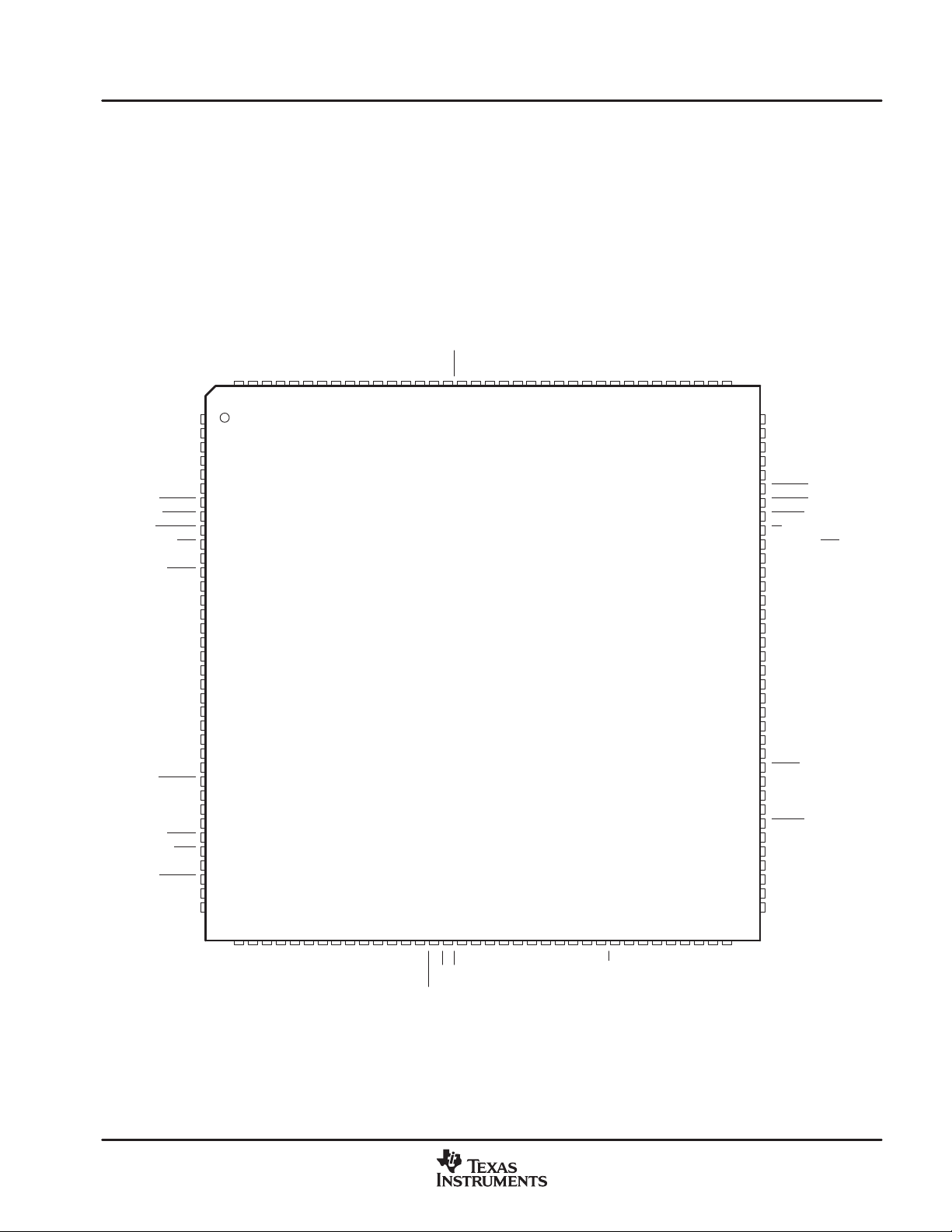
Figure 2–1 provides the pin assignments for the 144-pin low-profile quad flatpack (LQFP) package.
Figure 2–2 illustrates the ball locations for the 144-pin ball grid array (BGA) package and is used in conjunction
with Table 2–2 to locate signal names and ball grid numbers.
2.3.1 Pin Assignments for the PGE Package
The TMS320VC5421PGE 144-pin low-profile quad flatpack (LQFP) is footprint- and pin-compatible with the
5420. Table 2–1 lists the pin number and associated signal name for both the multiplexed mode and the
nonmultiplexed mode.
Introduction
PPD7
PPA8
PPA0
DV
DD
PPA9
PPD1
A_INT1
A_NMI
IOSTRB
A_GPIO2/BIO
A_GPIO1
A_RS
A_GPIO0
V
V
CV
DD
A_BFSR1
A_BDR1
A_BCLKR1
A_BFSX1
CV
DD
V
A_BDX1
A_BCLKX1
A_XF
A_CLKOUT
HOLDA
TCK
TMS
TDI
TRST
EMU1/OFF
DV
DD
A_INT0
EMU0
TDO
DD
SS
PPD4
PPD0
PPD5
PPD6
A_BFSX2
141
140
A_BDX2
139
138
V
144
143
142
1
2
3
4
5
6
7
8
9
10
11
12
13
14
SS
15
SS
16
17
18
19
20
21
22
SS
23
24
25
26
27
28
29
30
31
32
33
34
35
36
373839404142434445464748495051525354555657585960616263646566676869
A_BFSR2
A_BDR2
A_BCLKR2
137
136
135
SS
V
134
A_BCLKX2
CV
133
132
DD
READY
131DV130
HOLD
CLKIN
129
128
SSA
V
127
AV
126
DD
V
SS
125
B_BCLKX2
124
B_BDX2
B_BFSX2
B_BCLKR2
123
122
121
CV
120
DD
SS
V
119
B_BDR2
PPD2
B_BFSR2
118
117
116
PPD3
PPA1
115
114
PPA5
113
DD
DV
112
PPA6
PPA4
111
110
707172
PPA7
109
108
107
106
105
104
103
102
101
100
PPA14
PPA15
V
PPA16
PPA17
B_INT0
B_INT1
B_NMI
IS
99
B_GPIO2/BIO
98
B_GPIO1
97
B_GPIO0
96
B_BFSR1
95
B_BDR1
94
CV
93
V
92
B_BCLKR1
91
B_BFSX1
90
V
89
B_BDX1
88
B_BCLKX1
87
CV
86
V
85
TEST
84
XIO
83
B_RS
82
B_XF
81
B_CLKOUT
80
HMODE
79
HPIRS
PPA13
78
77
PPA12
V
76
DV
75
PPA11
74
PPA10
73
SS
DD
SS
SS
DD
SS
SS
DD
PS
MSTRB
A_BDX0
A_BCLKX0
DS
DD
DV
B_BDX0
B_BCLKX0
SS
V
B_BFSX0
SS
DD
V
CV
B_BDR0
B_BCLKR0
R/W
PPA2
B_BFSR0
PPA3
PPD8
SELA/B
PPD9
PPD10
SS
V
PPD11
SS
V
PPD15
V
PPD14SSPPD13
PPD12
A_BDR0
A_BFSR0
A_BCLKR0
SS
DD
V
CV
A_BFSX0
NOTES: A. DVDD is the power supply for the I/O pins while CVDD is the power supply for the core CPU. VSS is the ground for both the I/O pins
and the core CPU.
B. Pin configuration shown for nonmultiplexed mode only. See the pin assignments table for the TMS320VC5421PGE for multiplexed
functions of specific pins and for specific pin numbers.
Figure 2–1. 144-Pin Low-Profile Flatpack Pin Assignments (PGE – Top View)
December 1999 – Revised November 2001 SPRS098C
3
Page 13

Introduction
Table 2–1. Pin Assignments for the 144-Pin Low-Profile Quad Flatpack
SIGNAL NAME
(NONMULTIPLEXED)
SIGNAL NAME
(MULTIPLEXED)
PIN
NO.
SIGNAL NAME
(NONMULTIPLEXED)
SIGNAL NAME
(MULTIPLEXED)
PIN
NO.
PPD7 HD7 1 PPA8 HA8 2
PPA0 A_HINT/HA0 3 DV
DD
PPA9 HA9 5 PPD1 HD1 6
A_INT1 7 A_NMI 8
IOSTRB A_GPIO3/A_TOUT 9 A_GPIO2/BIO 10
A_GPIO1 11 A_RS 12
A_GPIO0 A_ROMEN 13 V
V
SS
15 CV
SS
DD
14
16
A_BFSR1 17 A_BDR1 18
A_BCLKR1 19 A_BFSX1 20
CV
DD
21 V
SS
22
A_BDX1 23 A_BCLKX1 24
A_XF 25 A_CLKOUT 26
HOLDA 27 TCK 28
TMS 29 TDI 30
TRST 31 EMU1/OFF 32
DV
DD
33 A_INT0 34
EMU0 35 TDO 36
V
SS
PPD14 HD14 39 V
37 PPD15 HD15 38
SS
40
PPD13 HD13 41 PPD12 HD12 42
A_BFSR0 43 A_BDR0 44
A_BCLKR0 45 A_BFSX0 46
V
SS
47 CV
DD
48
A_BDX0 49 A_BCLKX0 50
MSTRB HCS 51 DS HDS2 52
PS HDS1 53 B_BCLKX0 54
B_BDX0 55 DV
V
SS
57 B_BFSX0 58
DD
56
B_BCLKR0 59 B_BDR0 60
CV
DD
61 V
SS
62
B_BFSR0 63 R/W HR/W 64
PPA2 HCNTL1/HA2 65 PPA3 HCNTL0/HA3 66
SELA/B PPA18 67 PPD8 HD8 68
PPD9 HD9 69 PPD10 HD10 70
PPD11 HD11 71 V
SS
72
PPA10 HA10 73 PPA11 HA11 74
DV
DD
75 V
SS
76
PPA12 HA12 77 PPA13 HA13 78
HPIRS 79 HMODE 80
B_CLKOUT 81 B_XF 82
B_RS 83 XIO 84
TEST 85 V
SS
86
4
4
December 1999 – Revised November 2001SPRS098C
Page 14

Table 2–1. Pin Assignments for the 144-Pin Low-Profile Quad Flatpack (Continued)
Introduction
SIGNAL NAME
(NONMULTIPLEXED)
CV
DD
SIGNAL NAME
(MULTIPLEXED)
PIN
NO.
87 B_BCLKX1 88
B_BDX1 89 V
SIGNAL NAME
(NONMULTIPLEXED)
SS
SIGNAL NAME
(MULTIPLEXED)
PIN
NO.
90
B_BFSX1 91 B_BCLKR1 92
V
SS
93 CV
DD
94
B_BDR1 95 B_BFSR1 96
B_GPIO0 B_ROMEN 97 B_GPIO1 98
B_GPIO2/BIO 99 IS B_GPIO3/B_TOUT 100
B_NMI 101 B_INT1 102
B_INT0 103 PPA17 HA17 104
PPA16 HA16 105 V
SS
106
PPA15 HA15 107 PPA14 HA14 108
PPA7 HA7 109 PPA6 HA6 110
PPA4 HAS/HA4 111 DV
DD
112
PPA5 HA5 113 PPA1 B_HINT/HA1 114
PPD3 HD3 115 PPD2 HD2 116
B_BFSR2 117 B_BDR2 118
V
SS
119 CV
DD
120
B_BCLKR2 121 B_BFSX2 122
B_BDX2 123 B_BCLKX2 124
V
SS
V
SSA
CLKIN 129 DV
125 AV
DD
126
127 HOLD 128
DD
130
READY HRDY 131 A_BCLKX2 132
CV
DD
133 V
SS
134
A_BCLKR2 135 A_BDR2 136
A_BFSR2 137 A_BDX2 138
A_BFSX2 139 PPD6 HD6 140
PPD4 HD4 141 PPD5 HD5 142
PPD0 HD0 143 V
SS
144
December 1999 – Revised November 2001 SPRS098C
5
Page 15
Introduction
2.3.2 Terminal Assignments for the GGU Package
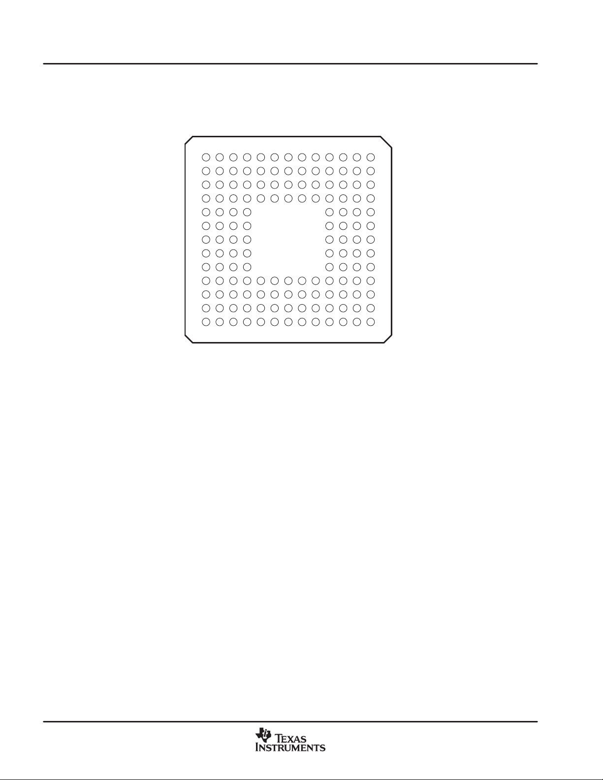
Table 2–2 lists each ball number and its associated signal name for the TMS320VC5421GGU 144-ball BGA
package, which is footprint- and pin-compatible with the 5420.
12
3456781012 1113 9
A
B
C
D
E
F
G
H
J
K
L
M
N
†
To locate the A1 reference maker, see package top view in Figure 6–1.
Figure 2–2. 144-Ball MicroStar BGA Pin Assignments (GGU – Bottom View)
6
December 1999 – Revised November 2001SPRS098C
Page 16
Introduction
Table 2–2. Terminal Assignments for the 144-Pin MicroStar BGA
SIGNAL NAME SIGNAL NAME BALL SIGNAL NAME SIGNAL NAME BALL
(NONMULTIPLEXED) (MULTIPLEXED) NO. (NONMULTIPLEXED) (MULTIPLEXED) NO.
PPD7 HD7 A1 PPA8 HA8 B1
DV
DD
A_RS E1 CV
A_BDR1 G1 CV
A_XF J1 TMS K1
EMU1/OFF L1 EMU0 M1
V
SS
V
SS
A_INT1 D2 A_GPIO1 E2
V
SS
V
SS
TDI K2 DV
TDO M2 PPD15 HD15 N2
PPD6 HD6 A3 PPD4 HD4 B3
PPD5 HD5 C3 PPD1 HD1 D3
A_GPIO2/BIO E3 V
A_BCLKR1 G3 A_BDX1 H3
HOLDA J3 TRST K3
A_INT0 L3 PPD14 HD14 M3
V
SS
A_BDX2 B4 A_BFSX2 C4
PPA9 HA9 D4 IOSTRB A_GPIO3/A_TOUT E4
A_GPIO0 A_ROMEN F4 A_BFSX1 G4
A_BCLKX1 H4 TCK J4
PPD13 HD13 K4 PPD12 HD12 L4
A_BFSR0 M4 A_BDR0 N4
CV
DD
A_BCLKR2 C5 A_BDR2 D5
A_BCLKR0 K5 A_BFSX0 L5
V
SS
CLKIN A6 DV
READY HRDY C6 A_BCLKX2 D6
A_BDX0 K6 A_BCLKX0 L6
MSTRB HCS M6 DS HDS2 N6
AV
DD
V
SSA
DV
DD
PS HDS1 M7 B_BCLKX0 N7
C1 A_NMI D1
DD
DD
F1
H1
N1 PPD0 HD0 A2
B2 PPA0 A_HINT/HA0 C2
F2 A_BFSR1 G2
H2 A_CLKOUT J2
DD
SS
L2
F3
N3 A_BFSR2 A4
A5 V
M5 CV
A7 V
SS
DD
DD
SS
B5
N5
B6
B7
C7 HOLD D7
K7 B_BDX0 L7
December 1999 – Revised November 2001 SPRS098C
7
Page 17

Introduction
Table 2–2. Terminal Assignments for the 144-Pin MicroStar BGA (Continued)
SIGNAL NAME BALLSIGNAL NAMESIGNAL NAMEBALLSIGNAL NAME
(NONMULTIPLEXED) NO.(MULTIPLEXED)(NONMULTIPLEXED)NO.(MULTIPLEXED)
B_BCLKX2 A8 B_BDX2 B8
B_BFSX2 C8 B_BCLKR2 D8
B_BDR0 K8 B_BCLKR0 L8
B_BFSX0 M8 V
CV
DD
A9 V
B_BDR2 C9 B_BFSR2 D9
R/W HR/W K9 B_BFSR0 L9
V
SS
M9 CV
PPD2 HD2 A10 PPD3 HD3 B10
PPA1 B_HINT/HA1 C10 PPA5 HA5 D10
IS B_GPIO3/B_TOUT E10 B_BFSR1 F10
B_BCLKR1 G10 TEST H10
B_CLKOUT J10 PPA12 HA12 K10
SELA/B PPA18 L10 PPA3 HCNTL0/HA3 M10
PPA2 HCNTL1/HA2 N10 DV
PPA4 HAS/HA4 B11 V
B_INT0 D11 B_GPIO2/BIO E11
B_BDR1 F11 B_BFSX1 G11
V
SS
H11 B_XF J11
PPA13 HA13 K11 PPD10 HD10 L11
PPD9 HD9 M11 PPD8 HD8 N11
PPA6 HA6 A12 PPA14 HA14 B12
PPA16 HA16 C12 B_INT1 D12
B_GPIO1 E12 CV
B_BDX1 G12 CV
B_RS J12 HPIRS K12
DV
DD
L12 V
PPD11 HD11 N12 PPA7 HA7 A13
PPA15 HA15 B13 PPA17 HA17 C13
B_NMI D13 B_GPIO0 B_ROMEN E13
V
SS
F13 V
B_BCLKX1 H13 XIO J13
HMODE K13 V
PPA11 HA11 M13 PPA10 HA10 N13
SS
SS
DD
DD
SS
DD
DD
SS
SS
SS
N8
B9
N9
A11
C11
F12
H12
M12
G13
L13
8
December 1999 – Revised November 2001SPRS098C
Page 18
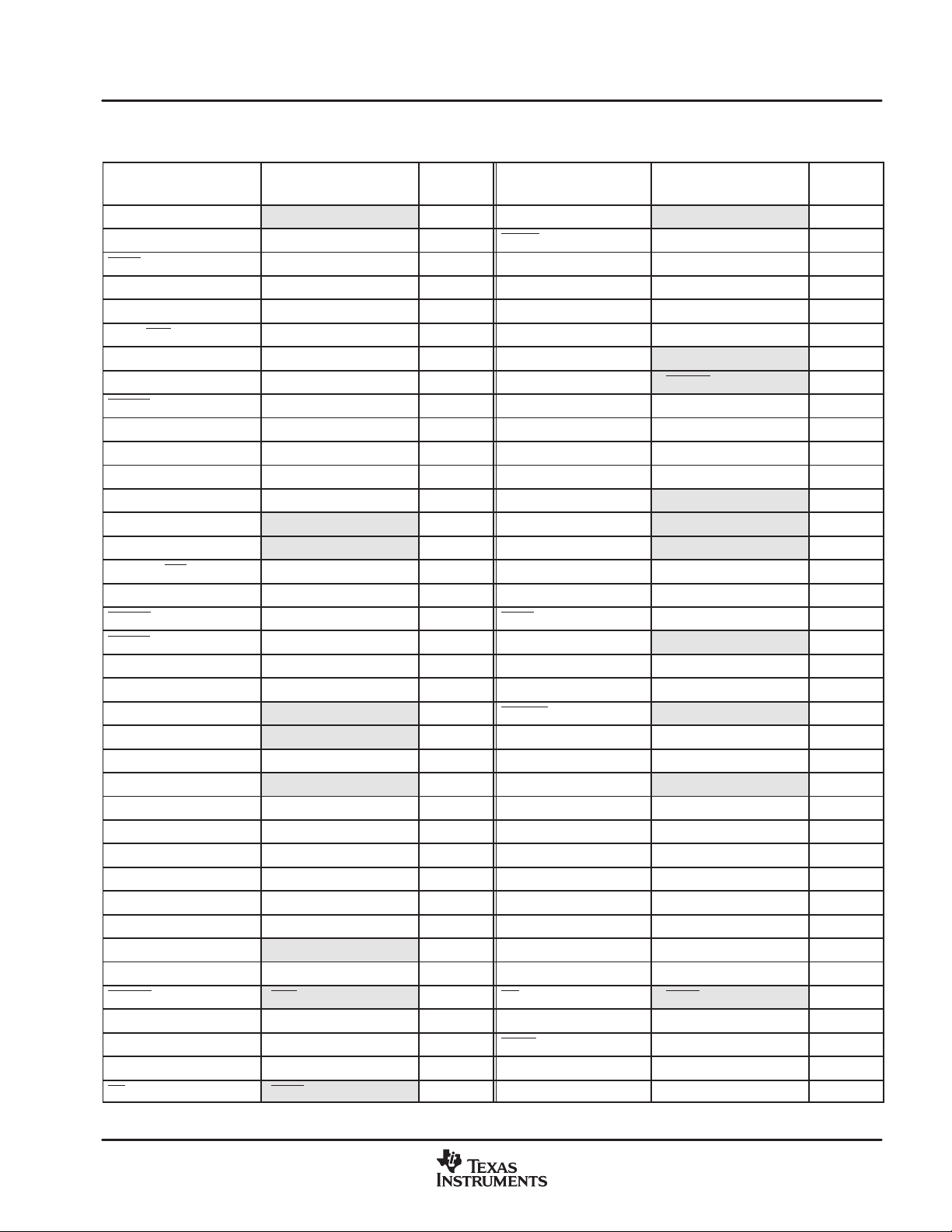
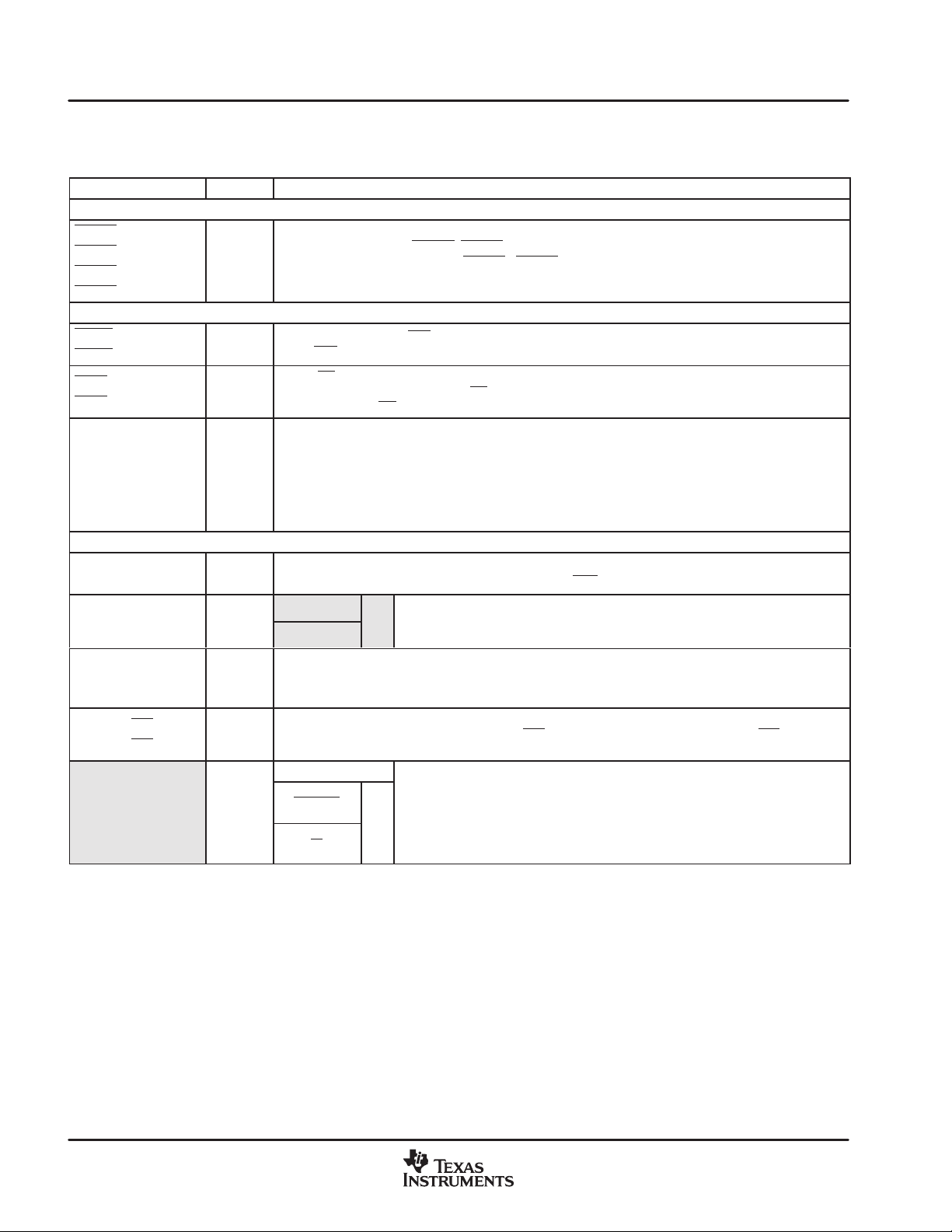
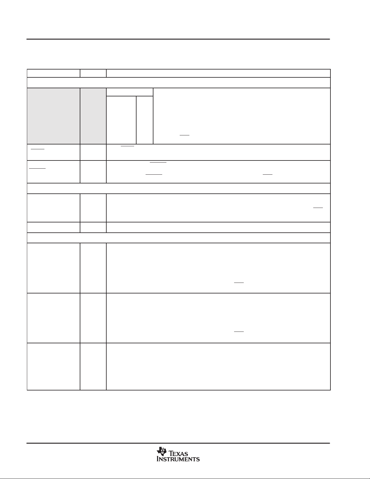
2.4 Signal Descriptions
Table 2–3 lists each signal, function, and operating mode(s) grouped by function. See pin assignments section
for exact pin locations based on package type.
Introduction
Table 2–3. Signal Descriptions
PIN NAME TYPE
†
DESCRIPTION
DATA SIGNALS
PPA18 (MSB)
PPA17
PPA16
PPA15
PPA14
PPA13
PPA12
PPA11
Parallel port address bus. The DSP can access the external memory locations by way of the external
memory interface using PPA[18:0] in external memory interface (EMIF) mode when the XIO pin is logic
high. PPA18 is a secondary output function of the SELA/B pin.
The PPA[17:0] pins are also multiplexed with the HPI interface. In HPI mode (XIO pin is low), the external
address pins PPA[17:0] are used by a host processor for access to the memory map by way of the on-chip
HPI. Refer to the Host-Port Interface (HPI) Signals section of this table for details on the secondary
functions of these pins.
These pins are placed into the high-impedance state when OFF
is low.
PPA10
PPA9
I/O/Z
PPA8
PPA7
PPA6
PPA5
‡§
PPA4
PPA3
PPA2
PPA1
PPA0 (LSB)
PPD15 (MSB)
PPD14
Parallel port data bus. The DSP uses this bidirectional data bus to access external memory when the
device is in external memory interface (EMIF) mode (the XIO pin is logic high).
PPD13
PPD12
PPD11
This data bus is also multiplexed with the 16-bit HPI data bus. When in HPI mode, the bus is used to transfer
data between the host processor and internal DSP memory via the HPI. Refer to the HPI section of this
table for details on the secondary functions of these pins.
PPD10
PPD9
PPD8
PPD7
PPD6
I/O/Z
The data bus includes bus holders to reduce power dissipation caused by floating, unused pins. The bus
holders also eliminate the need for external pullup resistors on unused pins. When the data bus is not being
¶
driven by the 5421, the bus holders keep data pins at the last driven logic level. The data bus keepers are
disabled at reset and can be enabled/disabled via the BH bit of the BSCR register.
PPD5
PPD4
These pins are placed into high-impedance state when OFF
is low.
PPD3
PPD2
PPD1
PPD0 (LSB)
†
I = Input, O = Output, S = Supply, Z = High Impedance
‡
This pin has an internal pullup resistor.
§
These pins are Schmitt triggered inputs.
¶
This pin has an internal bus holder controlled by way of the BSCR register in 54x cLEAD core of DSP subsystem A .
#
This pin is used by Texas Instruments for device testing and should be left unconnected.
||
This pin has an internal pulldown resistor.
December 1999 – Revised November 2001 SPRS098C
9
Page 19
Introduction
Table 2–3. Signal Descriptions (Continued)
PIN NAME DESCRIPTIONTYPE
†
DATA SIGNALS (CONTINUED)
§
A_INT0
B_INT0
A_INT1
B_INT1
§
§
§
External user interrupts. A_INT0–B_INT0 are prioritized and are maskable by the interrupt mask register
(IMR) and the interrupt mode bit. A_INT1
I
–B_INT1 can be polled and reset by way of the interrupt flag
register (IFR).
INITIALIZATION, INTERRUPT, AND RESET OPERATIONS
§
A_NMI
B_NMI
A_RS
B_RS
§
§
§
Nonmaskable interrupt. NMI is an external interrupt that cannot be masked by way of the INTM or the IMR.
I
When NMI
is activated, the processor traps to the appropriate vector location.
Reset. RS causes the digital signal processor (DSP) to terminate execution and causes a reinitialization
of the CPU and peripherals. When RS
I
program memory. RS
affects various registers and status bits.
is brought to a high level, execution begins at location 0FF80h of
The XIO pin is used to configure the parallel port as a host-port interface (HPI mode when XIO pin is low),
or as an asynchronous memory interface (EMIF mode when XIO pin is high).
XIO I
NOTE: Because the XIO signal is asynchronous, caution must be taken when changing the state of the
XIO pin to ensure the current cycle is properly ended.
At device reset, the XIO pin level determines the initialization value of the MP/MC bit (a bit in the processor
mode status (PMST) register). Refer to the memory section for details.
GENERAL-PURPOSE I/O PINS
A_XF
B_XF
A_GPIO0
A_GPIO0
B_GPIO0
A_GPIO1
B_GPIO1
A_GPIO2/BIO
B_GPIO2/BIO
O/Z
I/O/Z
I/O/Z
I/O/Z
External flag output (latched software-programmable output-only signal). Bit-addressable. A_XF and
B_XF are placed into the high-impedance state when OFF
A_ROMEN
B_ROMEN
General-purpose I/O pins. The secondary function of these pins. In XIO mode, the
ROM enable (ROMEN) pins are used to enable the applicable on-chip ROM after
I
reset.
is low.
General-purpose I/O pins (software-programmable I/O signal). Values can be latched (output) by writing into the GPIO register. The states of GPIO pins (inputs) can be read by reading the GPIO register.
The GPIO direction is also programmable by way of the DIRn field in the GPIO register.
General-purpose I/O. These pins can be configured like GPIO0–GPIO1; however, as an input, the pins
operate as the traditional branch control bit (BIO
). If application code does not perform BIO-conditional
instructions, these pins operate as general inputs.
PRIMARY
A_GPIO3 (A_TOUT)
B_GPIO3 (B_TOUT)
I/O/Z
IOSTRB
IS
†
I = Input, O = Output, S = Supply, Z = High Impedance
‡
This pin has an internal pullup resistor.
§
These pins are Schmitt triggered inputs.
¶
This pin has an internal bus holder controlled by way of the BSCR register in 54x cLEAD core of DSP subsystem A .
#
This pin is used by Texas Instruments for device testing and should be left unconnected.
||
This pin has an internal pulldown resistor.
When the device is in HPI mode and HMODE = 0 (multiplexed), these pins act
according to the general-purpose I/O control register. TOUT bit must be set to “1”
to drive the timer output on the pin. IF TOUT = 0, then these pins are
O
general-purpose I/Os. In EMIF mode (XIO = 1), these signals are active during I/O
space accesses.
10
December 1999 – Revised November 2001SPRS098C
Page 20
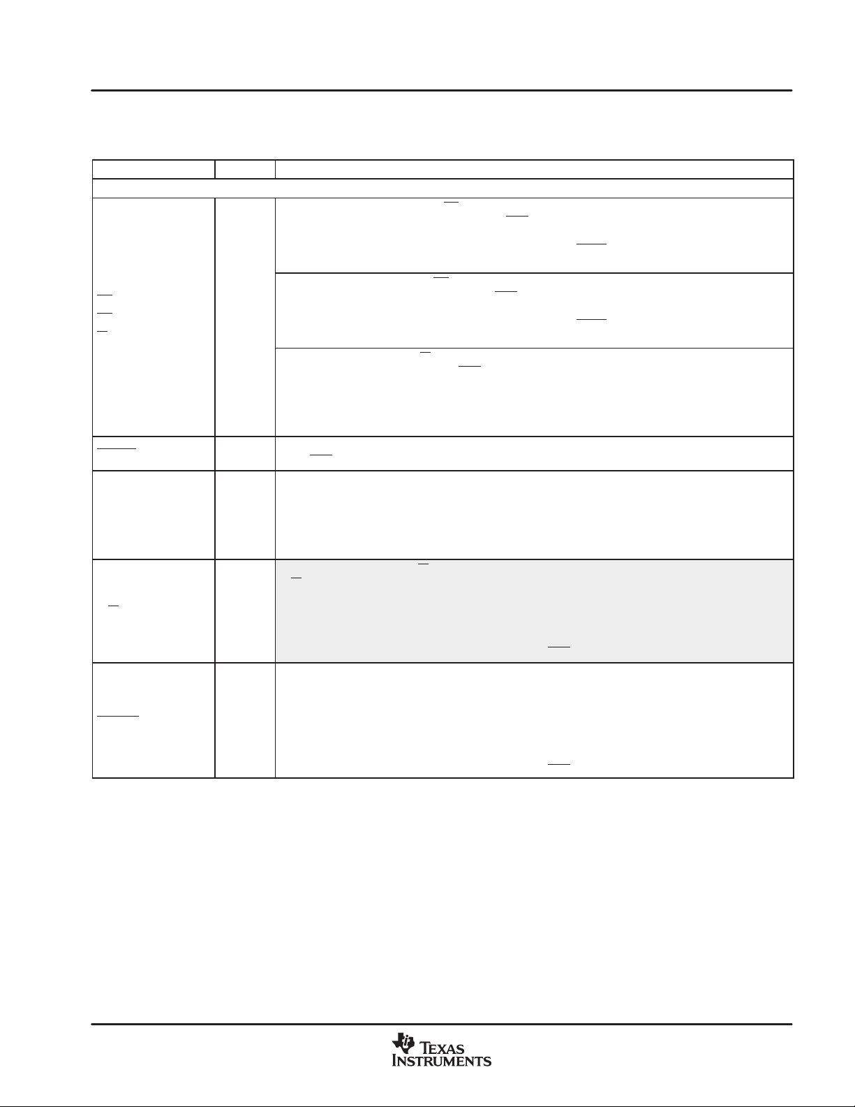
Table 2–3. Signal Descriptions (Continued)
Introduction
PIN NAME DESCRIPTIONTYPE
‡§
PS
‡§
DS
IS
‡§
MSTRB
READY I
O/Z
O/Z
†
MEMORY CONTROL SIGNALS
Program space select signal. The PS signal is asserted during external program space accesses. This pin
is placed into the high-impedance state when OFF
is low.
This pin is also multiplexed with the HPI, and functions as the HDS1 data strobe input signal in HPI mode.
Refer to the HPI section of this table for details on the secondary function of this pin.
Data space select signal. The DS signal is asserted during external data space accesses. This pin is
placed into the high-impedance state when OFF
is low.
This pin is also multiplexed with the HPI, and functions as the HDS2 data strobe input signal in HPI mode.
Refer to the HPI section of this table for details on the secondary function of this pin.
I/O space select signal. The IS signal is asserted during external I/O space accesses. This pin is placed
into the high-impedance state when OFF
is low.
This pin is also multiplexed with the general-purpose I/O feature, and functions as the B_GPIO3 (B_TOUT)
input/output signal in HPI mode. Refer to the General-Purpose I/O section of this table for details on the
secondary function of this pin.
Program and data memory strobe (active in EMIF mode). This pin is placed into the high-impedance state
when OFF
is low.
Data-ready input signal. READY indicates that the external device is prepared for a bus transaction to be
completed. If the device is not ready (READY = 0), the processor waits one cycle and checks READY
again. The processor performs the READY detection if at least two software wait states are programmed.
This pin is also multiplexed with the HPI, and functions as the host-port data ready (output) in HPI mode.
Refer to the HPI section of this table for details on the secondary function of this pin.
Read/write output signal. R/W indicates transfer direction during communication to an external device.
R/W
is normally in the read mode (high), unless it is asserted low when the DSP performs a write operation.
R/W O/Z
This pin is also multiplexed with the HPI, and functions as the host-port read/write input in HPI mode. Refer
to the HPI section of this table for details on the secondary function of this pin.
This pin is placed into the high-impedance state when OFF
is low.
I/O space memory strobe. External I/O space is accessible by the CPU and not the direct memory access
(DMA) controller. The DMA has its own dedicated I/O space that is not accessible by the CPU.
IOSTRB O/Z
This pin is also multiplexed with the general-purpose I/O feature, and functions as the A_GPIO3 (A_TOUT)
signal in HPI mode. Refer to the General Purpose I/O section of this table for details on the secondary
function of this pin.
This pin is placed into the high-impedance state when OFF
†
I = Input, O = Output, S = Supply, Z = High Impedance
‡
This pin has an internal pullup resistor.
§
These pins are Schmitt triggered inputs.
¶
This pin has an internal bus holder controlled by way of the BSCR register in 54x cLEAD core of DSP subsystem A .
#
This pin is used by Texas Instruments for device testing and should be left unconnected.
||
This pin has an internal pulldown resistor.
is low.
December 1999 – Revised November 2001 SPRS098C
11
Page 21
Introduction
Table 2–3. Signal Descriptions (Continued)
PIN NAME DESCRIPTIONTYPE
PPA18 O/Z
‡
HOLD
HOLDA O/Z
A_CLKOUT
B_CLKOUT
§
CLKIN
A_BCLKR0
B_BCLKR0
A_BCLKR1
B_BCLKR1
A_BCLKR2
B_BCLKR2
A_BCLKX0
B_BCLKX0
A_BCLKX1
B_BCLKX1
A_BCLKX2
B_BCLKX2
‡§
‡§
‡§
‡§
‡§
‡§
‡§
‡§
‡§
‡§
‡§
‡§
O/Z
I/O/Z
I/O/Z
†
MEMORY CONTROL SIGNALS (CONTINUED)
PRIMARY
For HPI access (XIO=0), SELA/B is an input.
See T able 3–3 for a truth table of SELA/B, HMODE, and XIO pins and functionality.
SELA/B I
For external memory accesses (XIO=1), SELA/B is multiplexed as output PPA18.
See the PPA signal descriptions. These pins are placed into the high-impedance
state when OFF
Hold. HOLD is asserted to request control of the address, data, and control lines. When acknowledged,
I
these lines go into the high-impedance state.
is low.
Hold acknowledge. HOLDA indicates to the external circuitry that the processor is in a hold state and that
the address, data, and control lines are in the high-impedance state, allowing them to be available to the
external circuitry. HOLDA
also goes into the high-impedance state when OFF is low.
CLOCKING SIGNALS
Master clock output signal. CLKOUT cycles at the machine-cycle rate of the CPU. The internal machine
cycle is bounded by the falling edges of this signal. The CLKOUT pin can be turned off by writing a “1” to
the CLKOFF bit of the PMST register. CLKOUT goes into the high-impedance state when EMU1/OFF is
low.
I Input clock to the device. CLKIN connects to an oscillator circuit/device (PLL).
MULTICHANNEL BUFFERED SERIAL PORT 0, 1, AND 2 SIGNALS
Receive clocks. BCLKR serves as the serial shift clock for the buffered serial-port receiver . Input from an
external clock source for clocking data into the McBSP. When not being used as a clock, these pins can
be used as general-purpose I/O by setting RIOEN = 1.
BCLKR can be configured as an output by the way of the CLKRM bit in the PCR register.
These pins are placed into the high-impedance state when OFF
is low.
Transmit clocks. Clock signal used to clock data from the transmit register. This pin can also be configured
as an input by setting the CLKXM = 0 in the PCR register. BCLKX can be sampled as an input by way of
the IN1 bit in the SPC register. When not being used as a clock, these pins can be used as general-purpose
I/O by setting XIOEN = 1.
These pins are placed into the high-impedance state when OFF
is low.
A_BDR0
B_BDR0
A_BDR1
B_BDR1
Buffered serial data receive (input) pin. When not being used as data-receive pins, these pins can be used
I
as general-purpose I/O by setting RIOEN = 1.
A_BDR2
B_BDR2
†
I = Input, O = Output, S = Supply, Z = High Impedance
‡
This pin has an internal pullup resistor.
§
These pins are Schmitt triggered inputs.
¶
This pin has an internal bus holder controlled by way of the BSCR register in 54x cLEAD core of DSP subsystem A .
#
This pin is used by Texas Instruments for device testing and should be left unconnected.
||
This pin has an internal pulldown resistor.
12
December 1999 – Revised November 2001SPRS098C
Page 22
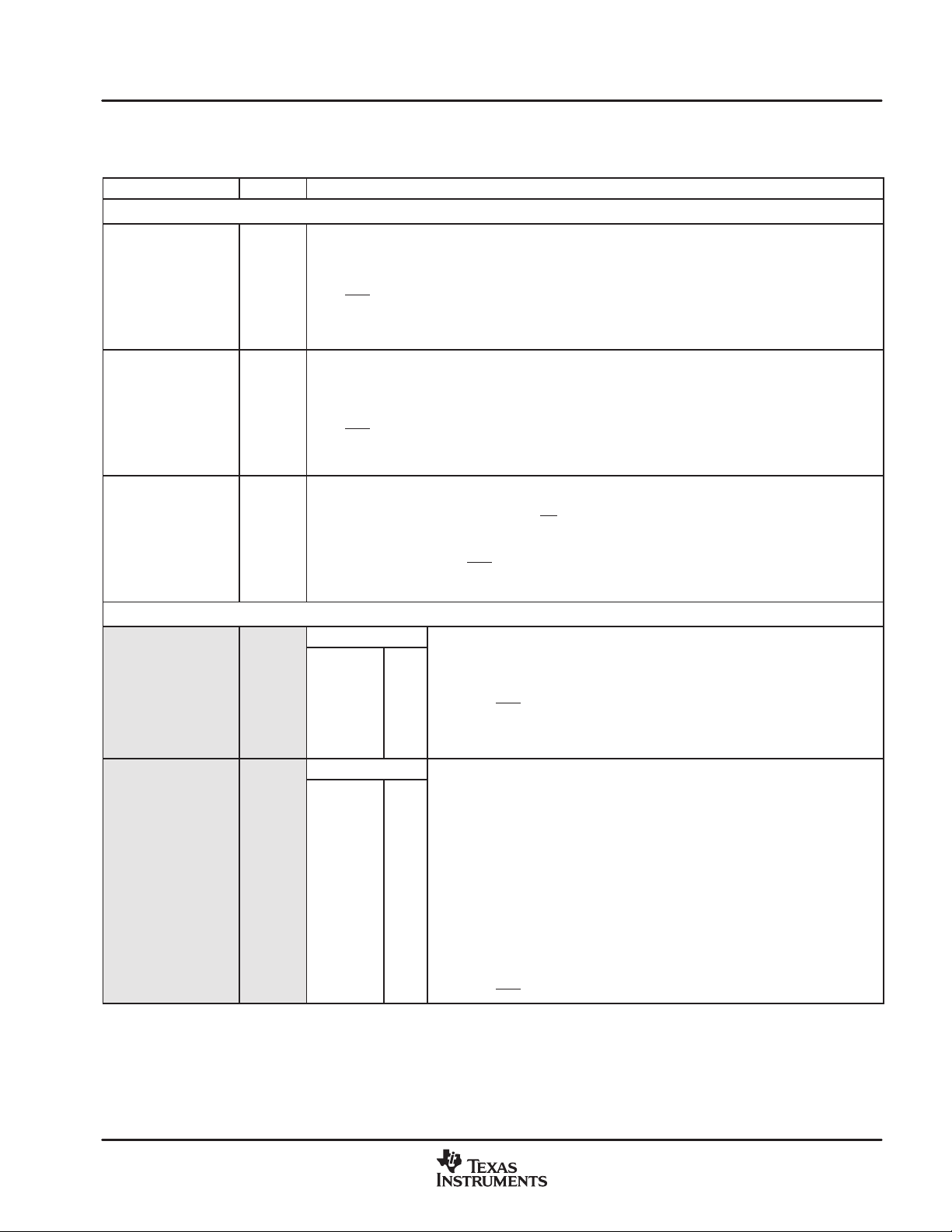
Table 2–3. Signal Descriptions (Continued)
Introduction
PIN NAME DESCRIPTIONTYPE
MULTICHANNEL BUFFERED SERIAL PORT 0, 1, AND 2 SIGNALS (CONTINUED)
A_BDX0
B_BDX0
A_BDX1
B_BDX1
A_BDX2
B_BDX2
A_BFSR0
B_BFSR0
A_BFSR1
B_BFSR1
I/O/Z
A_BFSR2
B_BFSR2
A_BFSX0
B_BFSX0
A_BFSX1
B_BFSX1
I/O/Z
A_BFSX2
B_BFSX2
HA[17:0] I
O/Z
†
Buffered serial-port transmit (output) pin. When not being used as data-transmit pins, these pins can be
used as general-purpose I/O by setting XIOEN = 1. These pins are placed into the high-impedance state
when OFF
is low.
Frame synchronization pin for buffered serial-port input data. The BFSR pulse initiates the receive-data
process over the BDR pin. When not being used as data-receive synchronization pins, these pins can be
used as general-purpose I/O by setting RIOEN = 1. These pins are placed into the high-impedance state
when OFF
is low.
Buffered serial-port frame synchronization pin for transmitting data. The BFSX pulse initiates the
transmit-data process over the BDX pin. If RS
is asserted when BFSX is configured as output, then BFSX
is turned into input mode by the reset operation. When not being used as data-transmit synchronization
pins, these pins can be used as general-purpose I/O by setting XIOEN = 1. These pins are placed into the
high-impedance state when OFF
is low.
HOST-PORT INTERFACE (HPI) SIGNALS
PRIMARY
These pins ar e m ultiplexed with the external interface pins and are used by the HPI
when the subsystem is in HPI mode (XIO = 0, MP/MC = 0).
PPA[17:0] O/Z
See the PPA signal descriptions. These pins are placed into the high-impedance
state when OFF
is low.
NOTE: HA4 has a pullup and a Schmitt trigger buffer.
PRIMARY
Parallel bidirectional data bus. These pins are multiplexed with the external
interface pins and are used as an HPI interface when XIO = 0.
These pins include bus holders to reduce power dissipation caused by floating,
unused inputs. The bus holders also eliminate the need for external pullup resistors
HD[15:0] I/O/Z
PPD[15:0] I/O/Z
on unused inputs. In multiplexed address/data mode (HMODE = 0), when the data
bus is not being driven by the 5421, the bus holders keep the multiplexed address
inputs on these pins at the last logic level driven by the host. The data bus holders
are disabled at reset and can be enabled/disabled via the BH bit of the BSCR
register.
See the PPD signal descriptions. These pins are placed into the high-impedance
state when OFF
†
I = Input, O = Output, S = Supply, Z = High Impedance
‡
This pin has an internal pullup resistor.
§
These pins are Schmitt triggered inputs.
¶
This pin has an internal bus holder controlled by way of the BSCR register in 54x cLEAD core of DSP subsystem A .
#
This pin is used by Texas Instruments for device testing and should be left unconnected.
||
This pin has an internal pulldown resistor.
is low.
December 1999 – Revised November 2001 SPRS098C
13
Page 23
Introduction
Table 2–3. Signal Descriptions (Continued)
PIN NAME DESCRIPTIONTYPE
†
HOST-PORT INTERFACE (HPI) SIGNALS (CONTINUED)
HPI control inputs. Use PPA3 and PP A2 for the HCNTL0 and HCNTL1 values during
the HPI HPIC, HPIA, and HPID reads/writes. Only used in multiplexed address/data
HCNTL0
HCNTL1
I
PPA3
PPA2
mode (HMODE = 0).
O/Z
These pins are shared with the external memory interface and are only used by the
HPI when the interface is in HPI mode (XIO pin is low). These pins are placed into
the high-impedance state when OFF
is low.
Address strobe input. Hosts with multiplexed address and data pins require HAS
to latch the address in the HPIA register. This signal is only used in HPI multiplexed
HAS
‡§
I PPA4
‡§
address/data mode (HMODE pin is low).
O/Z
This pin is shared with the external memory interface and is only used by the HPI
when the interface is in HPI mode (XIO pin is low). This pin is placed into the
high-impedance state when OFF
is low.
HPI chip-select signal. This signal must be active during HPI transfers, and can
remain active between concurrent transfers.
HCS
‡§
I MSTRB
‡§
O/Z
This pin is shared with the external memory interface and is only used by the HPI
when the interface is in HPI mode (XIO pin is low). This pin is placed into the
high-impedance state when OFF
is low.
HPI data strobes. HDS1 and HDS2 are driven by the host read and write strobes
HDS1
HDS2
‡§
‡§
I
PS
DS
‡§
‡§
to control HPI transfers.
These pins are shared with the external memory interface and are only used by the
O/Z
HPI when the interface is in HPI mode (XIO pin is low).
These pins are placed into the high-impedance state when OFF
HPI read/write signal. This signal is used by the host to control the direction of an
HPI transfer.
HR/W I R/W O/Z
This pin is shared with the external memory interface and is only used by the HPI
when the interface is in HPI mode (XIO pin is low).
This pin is placed into the high-impedance state when OFF
HPI data-ready output. The ready output informs the host when the HPI is ready for
the next transfer.
HRDY O/Z READY I
This pin is shared with the external memory interface and is only used by the HPI
when the interface is in HPI mode (XIO pin is low). HRDY is placed into the
high-impedance state when OFF
is low.
PRIMARY
A_HINT
B_HINT
O/Z
PPA0
PPA1
Host interrupt pin. HPI can interrupt the host by asserting this low. The host can clear
this interrupt by writing a “1” to the HINT
O/Z
HPI multiplexed address/data mode (HMODE pin is low). These pins are placed into
bit of the HPIC register. Only supported in
the high-impedance state when OFF is low.
§
HPIRS
†
I = Input, O = Output, S = Supply, Z = High Impedance
‡
This pin has an internal pullup resistor.
§
These pins are Schmitt triggered inputs.
¶
This pin has an internal bus holder controlled by way of the BSCR register in 54x cLEAD core of DSP subsystem A .
#
This pin is used by Texas Instruments for device testing and should be left unconnected.
||
This pin has an internal pulldown resistor.
I Host-port interface (HPI) reset pin. This signal resets the host port interface and both subsystems.
is low.
is low.
14
December 1999 – Revised November 2001SPRS098C
Page 24
Table 2–3. Signal Descriptions (Continued)
Introduction
PIN NAME DESCRIPTIONTYPE
†
HOST-PORT INTERFACE (HPI) SIGNALS (CONTINUED)
Host mode select. When this pin is low, it selects the HPI multiplexed address/data mode. The multiplexed
address/data mode allows hosts with multiplexed address/data lines access to the HPI registers HPIC,
HPIA, and HPID. Host-to-DSP and DSP-to-host interrupts are supported in this mode.
HMODE I
When HMODE is high, it selects the HPI nonmultiplexed mode. HPI nonmultiplexed mode allows hosts
with separate address/data buses to access the HPI address range by way of the 18-bit address bus and
the HPI data (HPID) register via the 16-bit data bus. Host-to-DSP and DSP-to-host interrupts are not
supported in this mode.
SUPPLY PINS
AV
CV
DV
V
V
DD
DD
DD
SS
SSA
S Dedicated power supply that powers the PLL. AVDD = 1.8 V. AVDD can be connected to CVDD.
S Dedicated “clean” power supply that powers the core CPUs. CVDD = 1.8 V
S Dedicated “dirty” power supply that powers the I/O pins. DVDD = 3.3 V
S Digital ground. Dedicated ground plane for the device.
Analog ground. Dedicated ground for the PLL. V
S
are not separated.
can be connected to VSS if digital and analog grounds
SSA
TEST PIN
#
TEST
No connection
EMULATION/TEST PINS
Standard test clock. This is normally a free-running clock signal with a 50% duty cycle. Changes on the
TCK
‡§
test access port (T AP) of input signals TMS and TDI are clocked into the TAP controller, instruction register,
I
or selected test-data register on the rising edge of TCK. Changes at the TAP output signal (TDO) occur
on the falling edge of TCK.
TDI
‡
Test data input. Pin with an internal pullup device. TDI is clocked into the selected register (instruction or
I
data) on a rising edge of TCK.
Test data output. The contents of the selected register is shifted out of TDO on the falling edge of TCK.
TDO O/Z
‡
TMS
||
TRST
TDO is in high-impedance state except when the scanning of data is in progress. These pins are
placed into high-impedance state when OFF
Test mode select. Pin with internal pullup device. This serial control input is clocked into the TAP controller
I
on the rising edge of TCK.
is low.
Test reset. When high, TRST gives the scan system control of the operations of the device. If TRST is
driven low, the device operates in its functional mode and the IEEE 1149.1 signals are ignored. Pin with
I
internal pulldown device.
†
I = Input, O = Output, S = Supply, Z = High Impedance
‡
This pin has an internal pullup resistor.
§
These pins are Schmitt triggered inputs.
¶
This pin has an internal bus holder controlled by way of the BSCR register in 54x cLEAD core of DSP subsystem A .
#
This pin is used by Texas Instruments for device testing and should be left unconnected.
||
This pin has an internal pulldown resistor.
December 1999 – Revised November 2001 SPRS098C
15
Page 25
Introduction
Table 2–3. Signal Descriptions (Continued)
PIN NAME DESCRIPTIONTYPE
†
EMULATION/TEST PINS (CONTINUED)
Emulator interrupt 0 pin. When TRST is driven low , EMU0 must be high for the activation of the EMU1/OFF
EMU0 I/O/Z
condition. When TRST is driven high, EMU0 is used as an interrupt to or from the emulator system and
is defined as I/O.
Emulator interrupt 1 pin. When TRST is driven high, EMU1/OFF is used as an interrupt to or from the
emulator system and is defined as I/O. When TRST
. EMU/OFF = 0 puts all output drivers into the high-impedance state.
OFF
EMU1/OFF I/O/Z
Note that OFF
applications). Therefore, for the OFF
= 0, EMU0 = 1, EMU1 = 0
TRST
†
I = Input, O = Output, S = Supply, Z = High Impedance
‡
This pin has an internal pullup resistor.
§
These pins are Schmitt triggered inputs.
¶
This pin has an internal bus holder controlled by way of the BSCR register in 54x cLEAD core of DSP subsystem A .
#
This pin is used by Texas Instruments for device testing and should be left unconnected.
||
This pin has an internal pulldown resistor.
is used exclusively for testing and emulation purposes (and not for multiprocessing
condition, the following conditions apply:
transitions from high to low, then EMU1 operates as
16
December 1999 – Revised November 2001SPRS098C
Page 26
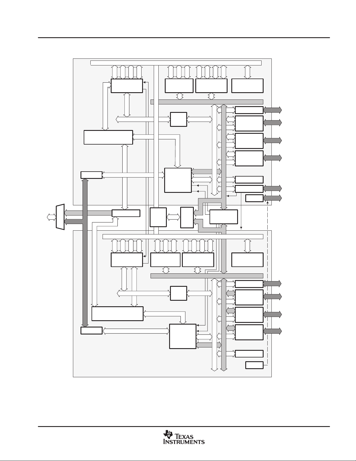
3 Functional Overview
Functional Overview
P, C, D, E Buses and Control Signals
DSP Subsystem A
XIO
16HPI
16 HPI
Arbitrator
Cbus
Dbus
Pbus
54X cLEAD
(Core A)
Arbitrator
Interprocessor
Ebus
TI BUS
IRQs
Cbus
Dbus
Ebus
32K RAM
Single Access
Data
RHEA
logic
RHEA Bus
Cycle
Arrangmnt
RHEAbus
Bridge
P bus
xDMA
128K
Dual
Access
PRAM
P
P, C, D, E Buses and Control Signals
Cbus
Dbus
Pbus
32K RAM
Dual Access
Program/Data
MBus
RHEA bus
MBus
Core-to-Core
FIFO Interface
MBus
Ebus
MBusMBus
Clocks
Pbus
2K Program
ROM
GPIO
McBSP1
McBSP2
McBSP3
TIMER
APLL
JTAG
16 HPI
DSP Subsystem B
Pbus
54X cLEAD
Arbitrator
(Core B)
Ebus
Cbus
Dbus
TI Bus
Host Access Bus
Cbus
Dbus
32K RAM
Single Access
Data
Ebus
RHEA
Bridge
xDMA
Logic
Pbus
Cbus
Dbus
32K RAM
Dual Access
Program/Data
MBus
RHEA Bus
MBus
Ebus
RHEA bus
MBus
Pbus
2K
Program ROM
GPIO
McBSP1
McBSP2
McBSP3
TIMER
JTAG
Figure 3–1. TMS320VC5421 Functional Block Diagram
December 1999 – Revised November 2001 SPRS098C
17
Page 27
Functional Overview
3.1 Memory
Each 5421 DSP subsystem maintains the peripheral register memory map and interrupt location/priorities of
the standard 5420. Figure 3–2 shows the size of the required memory blocks and their link map within the
program and data space of the cLEAD core. The total on-chip memory for the 5421 devices is 256K-word
data/program.
DataHex Program Page 0Hex
00 0000
00 005F
00 0060
00 7FFF
00 8000
00 FFFF
†
ROM enabled after reset.
‡
When CPU PMST register bit MP/MC=0 and an address is generated outside the on-chip memory bound or the address reach, i.e.,
Memory-
Mapped
Registers
On-Chip
DARAM A/B
(32K Words)
Prog/Data
On-Chip
SARAM A/B
(32K Words)
Data Only
(DROM=1)
External
(DROM=0)
00 0000
00 005F
00 0060
§
00 7FFF
00 8000
00 DFFF
00 E000
00 F7FF
00 F800
00 FFFF
Reserved
On-Chip
DARAM A/B
(32K Words)
Prog/Data
(OVLY=1)
External
(OVLY=0)
On-Chip
two-way
shared
DARAM 0
(24K Words)
Prog Only
Shared 0
Reserved
ROM
(ROMEN=1)
01 0000
01 005F
01 0060
§
01 7FFF
01 8000
¶
†
01 FFFF
XPC > 3h, access is always external, if XIO = 1. Pages 8–127 are mapped over pages 4–7. When XIO = 1 and MP/MC
1, 2, and 3 are external. Pages 4–127 are mapped over pages 0–3.
§
On-chip DARAM A and SARAM A are for subsystem A. Likewise, on-chip DARAM B and SARAM B are for subsystem B.
¶
On-chip DRAM 0 and DRAM 1 are owned by subsystem A and shared with subsystem B.
#
On-chip DRAM 2 and DRAM 3 are owned by subsystem B and shared with subsystem A.
Program Page 1Hex
Reserved
On-Chip
Prog/Data
(OVLY=1)
External
(OVLY=0)
On-Chip
two-way
shared
Prog Only
Shared 1
§
¶
02 FFFF
DARAM A/B
(32K Words)
DARAM 1
(32K Words)
(extended) (extended)
02 0000
02 005F
02 0060
02 7FFF
02 8000
Program Page 2Hex
Reserved
On-Chip
DARAM A/B
(32K Words)
Prog/Data
(OVLY=1)
External
(OVLY=0)
On-Chip
two-way
shared
DARAM 2
(32K Words)
Prog Only
Shared 2
Program Page 3Hex
03 0000
Reserved
03 005F
03 0060
§
03 7FFF
03 8000
#
03 FFFF
On-Chip
DARAM A/B
(32K Words)
Prog/Data
(OVLY=1)
External
(OVLY=0)
On-Chip
two-way
shared
DARAM 3
(32K Words)
Prog Only
Shared 3
(extended)
0n 0000
0n 005F
0n 0060
§
0n 7FFF
0n 8000
#
0n FFFF
Program Page nHex
Reserved
External
External
(n = 4 – 127)
= 1, program pages 0,
NOTES: A. Clearing the ROMEN bit (GPIO[7]) enables an 8K-word block (0E000h – 0FFFFh) of DARAM .
B. All external accesses require the XIO pin to be high.
C. CPU I/O space is a single page of 64K words. Access is always external.
D. All internal memory is divided into 8K blocks.
‡
‡
Figure 3–2. Memory Map Relative to CPU Subsystems A and B
3.1.1 On-Chip Dual-Access RAM (DARAM)
The 5421 subsystems A and B each have 32K 16-bit words of on-chip DARAM (4 blocks of 8K words). Each
of these DARAM blocks can be accessed twice per machine cycle. This memory is intended primarily to store
data values; however, it can be used to store program as well. At reset, the DARAM is mapped into data
memory space. The DARAM can be mapped into program/data memory space by setting the OVLY bit in the
processor-mode status (PMST) register of the 54x CPU in each DSP subsystem.
18
December 1999 – Revised November 2001SPRS098C
Page 28
3.1.2 On-Chip Single-Access RAM (SARAM)
The 5421 subsystems A and B each have 32K 16-bit words of on-chip SARAM (4 blocks of 8K words). Each
of these SARAM blocks can be accessed once per machine cycle. This memory is intended to store data
values only. At reset, the SARAM is disabled. The SARAM can be enabled in data memory space by setting
the DROM bit in the PMST register.
3.1.3 On-Chip Two-Way Shared RAM (DARAM)
The 5421 has 128K 16-bit words of on-chip DARAM (16 blocks of 8K words) that is shared between the two
DSP subsystems. This memory is intended to store program only. Each subsystem is able to make one
instruction fetch from any location in two-way shared memory each cycle. Neither subsystem CPU can write
to the two-way shared memory as only the DMA can write to two-way shared memory.
3.1.4 On-Chip Boot ROM
The 5421 subsystems A and B each have 2K 16-bit words of on-chip ROM. This ROM is used for bootloading
functions only. Enabling the ROM maps out one 8K-word block of the shared program memory . The ROM can
be disabled by clearing bit 7 (ROMEN) of the general-purpose I/O (GPIO) register. Table 3–1 shows the
XIO/ROMEN modes. The ROM is enabled or disabled at reset for each subsystem depending on the state
of the GPIO0 pin for that subsystem.
Table 3–1. XIO/ROMEN Modes
XIO ROMEN/GPIO0 MODE
0 x Fetch internal from RAM
1 0 Fetch external
1 1 ROM enabled
Functional Overview
3.1.5 Extended Program Memory
The program memory space on the 5421 device addresses up to 512K 16-bit words. The 5421 device uses
a paged extended memory scheme in program space to allow access of up to 512K of program memory . This
extended program memory (each subsystem) is organized into eight pages (0–7), pages 0–3 are internal,
pages 4–7 are external, each 64K in length. (Pages 8–127 as defined by the program counter extension
register (XPC) are aliases for pages 4–7.) Access to the extended program memory is similar to the 5420. To
implement the extended program memory scheme, the 5421 device includes the following feature:
• Two 54x instructions are extended to use the additional two bits in the 5421 device.
– READA – Read program memory addressed by accumulator A and store in data memory
– WRITA – Write data to program memory addressed by accumulator A
(Writes not allowed for CPUs to shared program memory)
December 1999 – Revised November 2001 SPRS098C
19
Page 29
Functional Overview
3.1.6 Program Memory
The program memory is accessible on multiple pages, depending on the XPC value. Within these pages,
memory is accessible, depending on the address range.
• Access in the lower 32K of each page is dependent on the state of OVLY.
– OVLY = 0 – Program memory is accessed externally for all values of XPC.
– OVLY = 1 – Program memory is accessed from local data/program DARAM for all values of XPC.
• Access in the upper 32K of each page is dependent on the state of MP/MC
– MP/MC
= 0 – Program memory is accessed internally from two-way shared DARAM for XPC = 0–3.
Program memory is accessed externally for XPC = 4–127.
– MP/MC
= 1 – Program memory is accessed externally for all values of XPC.
3.1.7 Data Memory
The data memory space is a single page of 64K. Access is dependent on the address range. Access in the
lower 32K of data memory is always from local DARAM.
Access in the upper 32K of data memory is dependent on the state of DROM.
• DROM = 0 – Data memory is accessed externally
• DROM = 1 – Data memory is accessed internally from local SARAM
3.1.8 I/O Memory
The I/O space is a single page of 64K. Access is always external.
and the value of XPC.
When XIO = 0 and an access to external memory is attempted, any write is ignored and any read is an unknown
value.
3.2 Multicore Reset Signals
The 5421 device includes three reset signals: A_RS, B_RS, and HPIRS. The A_RS and B_RS pins function
as the CPU reset signal for subsystem A and subsystem B, respectively. These signals reset the state of the
CPU registers and upon release, initiate the reset function. Additionally, the A_RS
PLL and initializes the CLKMD register to bypass mode.
The HPI reset signal (HPIRS
) places the HPI peripheral into a reset state. It is necessary to wait three clock
cycles after the rising edge of HPIRS
by turning off the PLL and initializing the CLKMD register to bypass mode.
3.3 Bootloader
The on-chip bootloader is used to automatically transfer user code from an external source to anywhere in
program memory after reset. The XIO pin is sampled during a hardware reset and the results indicate the
operating mode as shown in Table 3–2.
Table 3–2. Bootloader Operating Modes
XIO AFTER RESET
HPI mode, bootload is controlled by host. The external host holds the 5421 in reset while it loads the on-chip
memory of one or both subsystems as determined by the SELA/B pin.
The host can release the 5421 from reset by either of the following methods:
1. If the A_RS
0
1 XIO mode. ROM is mapped in, if ROMEN pin = 1 during reset.
be controlled by the A_RS
high to release the cores from reset.
2. If the A_RS
until a HPI data write to address 0x2F occurs. This means the host can download code to subsystem A and
then release core A from reset by writing any data to core A address 0x2F via the HPI. The host can then repeat
the sequence for core B. This mode allows the host to control the 5421 reset without additional hardware.
signal resets the on-chip
before performing an HPI access. The HPIRS signal also resets the PLL
/B_RS pins are held low while HPIRS transitions from low to high, the subsystem cores reset will
/B_RS pins. When the host has finished downloading code, it drives A_RS/B_RS
/B_RS pins are held high while HPIRS transitions from low to high, the subsystems stay in reset
20
December 1999 – Revised November 2001SPRS098C
Page 30
The 5421 bootloader provides the following options for the source of code to download:
• Parallel from 8-bit or 16-bit-wide EPROM
• Serial boot from McBSPs, 8-bit mode
GPIO register bit 7 (ROMEN) is used to enable/disable the ROM after reset. The ROMEN bit reflects the status
of the ROMEN/GPIO0 pin for each core. ROMEN = 1 indicates that the ROM and the 8K-word program
memory block (00 E000h–00 FFFFh) are not available for a CPU write. When ROMEN = 0, this 8K-word
program memory is available and the ROM is disabled.
A combination of interrupt flags and the bit values of an external memory location determine the selection of
the various boot options.
3.4 External Interface (XIO)
The external interface (XIO) supports the 5421 master boot modes and other external accesses. Its features
include:
• Multiplexed with the HPI pins
• Selection of XIO or HPI mode is determined by a dedicated pin (XIO)
• Provides 512K words of external program space, 64K words of external data space, and 64K words of
external I/O space.
• Different boot modes are selectable by the XIO, HMODE, and A_RS
• After reset, the control register bit ROMEN is always preset to 1.
Functional Overview
/B_RS pins.
While XIO = 0 during reset, host HPI mode is on, the host sees all RAM, and ROM is disabled. A host write
to 002Fh releases the CPUs from reset; the 002Fh write by the host clears the ROMEN bit in the GPIO register.
While XIO = 1 and ROMEN = 1 during reset, the CPU starts from ROM (0FF80h) to do boot selection. After
branching to non-ROM area, the code changes the ROMEN bit to enable the RAM area occupied by ROM.
While XIO = 1 and ROMEN = 0 during reset, the CPU starts from external (0FF80h) to do boot selection.
Table 3–3 provides a complete description of HMODE, SELA/B, and XIO pin functionality.
HMODE SELA/B HPI MODES (XIO = 0) XIO MODES (XIO = 1)
0 0 HPI muxed address/data subsystem A slave to host SELA/B pin is multiplexed as PPA18 output.
0 1
1 0
1 1
HPI muxed address/data subsystem B slave to host
HPI non-muxed address/data subsystem A slave to host
HPI non-muxed address/data subsystem B slave to host
3.5 On-Chip Peripherals
All the 54x devices have the same CPU structure; however, they have different on-chip peripherals connected
to their CPUs. The on-chip peripheral options provided are:
• Software-programmable wait-state generator
• Programmable bank-switching
• Parallel I/O ports
• Multichannel buffered serial ports (McBSPs)
• A hardware timer
• A software-programmable clock generator using a phase-locked loop (PLL)
Table 3–3. XIO/HPI Modes
SELA/B pin is multiplexed as PPA18 output.
SELA/B pin is multiplexed as PPA18 output.
SELA/B pin is multiplexed as PPA18 output.
December 1999 – Revised November 2001 SPRS098C
21
Page 31

Functional Overview
3.5.1 Software-Programmable Wait-State Generators
The software-programmable wait-state generator can be used to extend external bus cycles up to fourteen
machine cycles to interface with slower off-chip memory and I/O devices. The software wait-state register
(SWWSR) controls the operation of the wait-state generator. The SWWSR of a particular DSP subsystem
(A or B) is used for the external memory interface, depending on the state of the xDMA/XIO arbitration logic
(see Direct Memory Access (DMA) Controller section 3.8 and Table 3–4. The 14 least significant bits (LSBs)
of the SWWSR specify the number of wait states (0–7) to be inserted for external memory accesses to five
separate address ranges. This allows a different number of wait states for each of the five address ranges.
Additionally, the software wait-state multiplier (SWSM) bit of the software wait-state control register (SWCR)
defines a multiplication factor of 1 or 2 for the number of wait states. At reset, the wait-state generator is
initialized to provide seven wait states on all external memory accesses. The SWWSR bit fields are shown
in Figure 3–3 and described in Table 3–4.
15 14 13 12 11 10 9 8 7 6 5 4 3 2 1 0
XPA
R/W=0 R/W=111 R/W=111 R/W=111 R/W=111 R/W=111
LEGEND: R = Read, W = Write
I/O Data Data Program Program
Figure 3–3. Software Wait-State Register (SWWSR) [Memory-Mapped Register (MMR) Address 0028h]
Table 3–4. Software Wait-State Register (SWWSR) Bit Fields
BIT
NO. NAME
15 XPA 0
14–12 I/O 1
11–9 Data 1
8–6 Data 1
5–3 Program 1
2–0 Program 1
RESET
RESET
VALUE
FUNCTION
Extended program address control bit. XPA is used in conjunction with the program space fields
(bits 0 through 5) to select the address range for program space wait states.
I/O space. The field value (0–7) corresponds to the base number of wait states for I/O space accesses
within addresses 0000–FFFFh. The SWSM bit of the SWCR defines a multiplication factor of 1 or 2 for
the base number of wait states.
Upper data space. The field value (0–7) corresponds to the base number of wait states for external data
space accesses within addresses 8000–FFFFh. The SWSM bit of the SWCR defines a multiplication
factor of 1 or 2 for the base number of wait states.
Lower data space. The field value (0–7) corresponds to the base number of wait states for external data
space accesses within addresses 0000–7FFFh. The SWSM bit of the SWCR defines a multiplication
factor of 1 or 2 for the base number of wait states.
Upper program space. The field value (0–7) corresponds to the base number of wait states for external
program space accesses within the following addresses:
XPA = 0: x8000–xFFFFh
XPA = 1: The upper program space bit field has no effect on wait states.
The SWSM bit of the SWCR defines a multiplication factor of 1 or 2 for the base number of wait states.
Program space. The field value (0–7) corresponds to the base number of wait states for external program
space accesses within the following addresses:
XPA = 0: x0000–x7FFFh
XPA = 1: 00000–3FFFFh
The SWSM bit of the SWCR defines a multiplication factor of 1 or 2 for the base number of wait states.
22
December 1999 – Revised November 2001SPRS098C
Page 32

Functional Overview
The software wait-state multiplier bit of the software wait-state control register (SWCR) is used to extend the
base number of wait states selected by the SWWSR. The SWCR bit fields are shown in Figure 3–4 and
described in Table 3–5.
15 14 13 12 11 10 9 8 7 6 5 4 3 2 1 0
Reserved SWSM
R/W=0 R/W=0
LEGEND: R = Read, W = Write
Figure 3–4. Software Wait-State Control Register (SWCR) [MMR Address 002Bh]
Table 3–5. Software Wait-State Control Register (SWCR) Bit Fields
PIN
NO. NAME
15–1 Reserved 0
0 SWSM 0
RESET
RESET
VALUE
FUNCTION
These bits are reserved and are unaffected by writes.
Software wait-state multiplier. Used to multiply the number of wait states defined in the SWWSR by a factor
of 1 or 2.
SWSM = 0: wait-state base values are unchanged (multiplied by 1).
SWSM = 1: wait-state base values are multiplied by 2 for a maximum of 14 wait states.
3.5.2 Programmable Bank-Switching
Programmable bank-switching can be used to insert one cycle automatically when crossing memory-bank
boundaries inside program memory or data memory space. One cycle can also be inserted when crossing
from program-memory space to data-memory space (54x) or one program memory page to another program
memory page. This extra cycle allows memory devices to release the bus before other devices start driving
the bus, thereby avoiding bus contention. The size of the memory bank for the bank-switching is defined by
the bank-switching control register (BSCR), as shown in Figure 3–5. The BSCR of a particular DSP subsystem
(A or B) is used for the external memory interface based on the xDMA/XIO arbitration logic. The BSCR bit
fields are described in Table 3–6.
15 14 13 12 11 10 9 8 7 6 5 4 3 2 1 0
BNKCMP PS-DS Reserved IPIRQ Reserved BH Reserved EXIO
R/W R/W R/W R/W R/W R/W
LEGEND: R = Read, W = Write
Figure 3–5. BSCR Register Bit Layout for Each DSP Subsystem
December 1999 – Revised November 2001 SPRS098C
23
Page 33

Functional Overview
Table 3–6. BSCR Register Bit Functions for Each DSP Subsystem
BIT
NO.
15–12 BNKCMP 1111
11 PS-DS 1
10–9 Reserved 0 These bits are reserved and are unaffected by writes.
8 IPIRQ 0
7–3 Reserved 0 These bits are reserved and are unaffected by writes.
2 BH 0
1 Reserved 0 This bit is reserved and is unaffected by writes.
0 EXIO 0
BIT
NAME
RESET
VALUE
FUNCTION
Bank compare. BNKCMP determines the external memory-bank size. BNKCMP is used to mask the four
most significant bits (MSBs) of an address. For example, if BNKCMP = 1111b, the four MSBs (bits 12–15)
are compared, resulting in a bank size of 4K words. Bank sizes of 4K words to 64K words are allowed.
Program read – data read access. PS-DS inserts an extra cycle between consecutive accesses of
program read and data read or data read and program read.
PS-DS = 0
No extra cycles are inserted by this feature.
PS-DS = 1
One extra cycle is inserted between consecutive data and program reads.
The IPIRQ bit is used to send an interprocessor interrupt to the other subsystem. IPIRQ=1 sends the
interrupt. IPIRQ must be cleared before subsequent interrupts can be made. Refer to the interrupts section
for more details.
Bus holder. BH controls the bus holder feature: BH is cleared to 0 at reset.
BH = 0
The bus holder is disabled.
BH = 1
The bus holder is enabled. When not driven, PPD[15:0] pins are held at the previous logic
level.
External bus interface off. The EXIO bit controls the external bus-off function.
EXIO = 0
The external bus interface functions as usual.
EXIO = 1
The address bus, data bus, and control signals become inactive after completing the
3.5.3 Parallel I/O Ports
The 5421 has a total of 64K words of I/O port address space. These ports can be addressed by PORTR and
PORTW. The IS
with external devices through the I/O ports while requiring minimal off-chip address-decoding logic. The
SELA/B pin selects which subsystem is accessing the external I/O space.
signal indicates the read/write access through an I/O port. The devices can interface easily
current bus cycle. Note that the DROM, MP/MC
HM bit of ST1 cannot be modified when the interface is disabled.
, and OVLY bits in the PMST and the
24
December 1999 – Revised November 2001SPRS098C
Page 34

3.6 16-Bit Bidirectional Host-Port Interface (HPI16)
The HPI16 is an enhanced 16-bit version of the TMS320C54x DSP 8-bit host-port interface (HPI). The HPI16
is designed to allow a 16-bit host to access the DSP on-chip memory, with the host acting as the master of
the interface.
3.6.1 HPI16 Memory Map
Figure 3–6 illustrates the available memory accessible by the HPI. Neither the CPU nor DMA I/O spaces can
be accessed using the host-port interface.
Functional Overview
Hex
00 0000
00 001F
00 0020
00 005F
00 0060
00 7FFF
00 8000
Page 0
Reserved
McBSP
DXR/DRR
MMRegs Only
On-Chip
DARAM A
(32K Words)
Prog/Data
Subsystem A
On-Chip
SARAM A
(32K Words)
Data Only
Hex
01 0000
01 7FFF
01 8000
Page 1
On-Chip
Two-Way
Shared
DARAM 0
(32K Words)
Program Only
Shared 0
On-Chip
Two-Way
Shared
DARAM 1
(32K Words)
Program Only
Hex
02 0000
02 001F
02 0020
02 005F
02 0060
02 7FFF
02 8000
Page 2
Reserved
McBSP
DXR/DRR
MMRegs Only
On-Chip
DARAM B
(32K Words)
Prog/Data
Subsystem B
On-Chip
SARAM B
(32K Words)
Data Only
Hex
03 0000
03 7FFF
03 8000
Page 3
On-Chip
Two-Way
Shared
DARAM 2
(32K Words)
Program Only
Shared 2
On-Chip
Two-Way
Shared
DARAM 3
(32K Words)
Program Only
00 FFFF
NOTES: A. All local memory is available to the HPI
Subsystem A
B. The encoder maps CPU A Data Page 0 into the HPI Page 0. CPU B Data Page 0 is mapped into the HPI Page 2. Pages 1 and 3
are the on-chip shared program memory.
C. In pages 00 and 02, in the range of 0020–005F, only the following memory mapped registers are accessible: 20,21,30,31,40,41 (read
only), 22,23,32,33,42,43 (write only).
01 FFFF
Shared 1
02 FFFF
Subsystem B
03 FFFF
Shared 3
Figure 3–6. Memory Map Relative to Host-Port Interface HPI16
December 1999 – Revised November 2001 SPRS098C
25
Page 35

Functional Overview
3.6.2 HPI Features
Some of the features of the HPI16 include:
• 16-bit bidirectional data bus
• Multiple data strobes and control signals to allow glueless interfacing to a variety of hosts
• Multiplexed and nonmultiplexed address/data modes
• 18-bit address bus used in nonmultiplexed mode to allow access to all internal memory (including internal
extended address pages)
• 18-bit address register used in multiplexed mode. Includes address autoincrement feature for faster
accesses to sequential addresses
• Interface to on-chip DMA module to allow access to entire internal memory space
• HRDY signal to hold off host accesses due to DMA latency
• Control register available in multiplexed mode only. Accessible by either host or DSP to provide host/DSP
interrupts, extended addressing, and data prefetch capability
• Maximum data rate of 33 megabytes per second (MBps) at 100-MHz DSP clock rate (no other DMA
channels active)
The HPI16 acts as a slave to a 16-bit host processor and allows access to the on-chip memory of the DSP.
There are two modes of operation as determined by the HMODE signal: multiplexed mode and nonmultiplexed
mode.
3.6.3 HPI Multiplexed Mode
In multiplexed mode, HPI16 operation is very similar to that of the standard 8-bit HPI, which is available with
other C54x DSP products. A host with a multiplexed address/data bus can access the HPI16 data register
(HPID), address register (HPIA), or control register (HPIC) via the HD bidirectional data bus. The host initiates
the access with the strobe signals (HDS1
HR/W
, and HAS signals. The DSP can interrupt the host via the HINT signal, and can stall host accesses via
the HRDY signal.
, HDS2, HCS) and controls the type of access with the HCNTL,
3.6.4 Host/DSP Interrupts
In multiplexed mode, the HPI16 offers the capability for the host and DSP to interrupt each other through the
HPIC register.
For host-to-DSP interrupts, the host must write a “1” to the DSPINT bit of the HPIC register. This generates
an interrupt to the DSP. This interrupt can also be used to wake the DSP from any of the IDLE 1,2, or 3 states.
Note that the DSPINT bit is always read as “0” by both the host and DSP. The DSP cannot write to this bit (see
Figure 3–7).
For DSP-to-host interrupts, the DSP must write a “1” to the HINT
via the HINT
HPIC register. Note that writing a “0” to the HINT
pin. The host acknowledges and clears this interrupt by also writing a “1” to the HINT bit of the
3.6.5 Emulation Considerations
The HPI16 can continue operation even when the DSP CPU is halted due to debugger breakpoints or other
emulation events.
3.6.6 HPI Nonmultiplexed Mode
In nonmultiplexed mode, a host with separate address/data buses can access the HPI16 data register (HPID)
via the HD 16-bit bidirectional data bus, and the address register (HPIA) via the 18-bit HA address bus. The
host initiates the access with the strobe signals (HDS1
with the HR/W
is not available in nonmultiplexed mode since there are no HCNTL signals available. All host accesses initiate
a DMA read or write access. Figure 3–7 shows a block diagram of the HPI16 in nonmultiplexed mode.
signal. The HPI16 can stall host accesses via the HRDY signal. Note that the HPIC register
bit of the HPIC register to interrupt the host
bit by either host or DSP has no effect.
, HDS2, HCS) and controls the direction of the access
C54x is a trademark of Texas Instruments.
26
December 1999 – Revised November 2001SPRS098C
Page 36

Functional Overview
HOST
Data[15:0]
Address[n:0]
R/W
Data strobes
Ready
HD[15:0]
HA[n:0]
HRDY
HR/W
HDS1, HDS2, HCS
Figure 3–7. Interfacing to the HPI-16 in Non-Multiplexed Mode
3.6.7 Other HPI16 System Considerations
3.6.7.1 Operation During IDLE
The HPI16 can continue to operate during IDLE1 or IDLE2 by using special clock management logic that turns
on relevant clocks to perform a synchronous memory access, and then turns the clocks back off to save power.
The DSP CPU does not wake up from the IDLE mode during this process.
HPI-16
HPID[15:0]
DMA
54x
CPU
Internal
memory
3.6.7.2 Downloading Code During Reset
The HPI16 can download code while the DSP is in reset. However, the system provides a pin (HPIRS) that
provides a way to take the HPI16 module out of reset while leaving the DSP in reset. The maximum HPI16
data rate is 33 MBps assuming no other DMA activity (100-MIPS DSP subsystem).
3.6.7.3 Performance Issues
On the 5421, the use of SELA/B is optional for access to all on-chip memory. However, with both the 5420 and
5421 implementation using two separate subsystems (subchips), the SELA/B pin is used to select the specific
HPI16 used to access memory.
SELA/B PIN SUBSYSTEM
0A
1B
Accesses to memory contained inside the same subsystem as the selected HPI16 will be faster. For accesses
to an HPI16 in a subsystem different than the memory being addressed, reads take an additional six cycles
and writes an extra five cycles. Therefore, for performance reasons, it is best to additionally decode SELA/B.
December 1999 – Revised November 2001 SPRS098C
27
Page 37

Functional Overview
3.7 Multichannel Buffered Serial Port (McBSP)
The 5421 device provides high-speed, full-duplex serial ports that allow direct interface to other C54x/LC54x
devices, codecs, and other devices in a system. There are six multichannel buffered serial ports (McBSPs)
on board (three per subsystem).
The McBSP provides:
• Full-duplex communication
• Double-buffer data registers, which allow a continuous data stream
• Independent framing and clocking for receive and transmit
In addition, the McBSP has the following capabilities:
• Direct interface to:
– T1/E1 framers
– MVIP switching-compatible and ST-BUS compliant devices
– IOM-2 compliant device
– AC97-compliant device
– Serial peripheral interface (SPI)
• Multichannel transmit and receive of up to 128 channels
• A wide selection of data sizes, including: 8, 12, 16, 20, 24, or 32 bits
•µ-law and A-law companding
• Programmable polarity for both frame synchronization and data clocks
• Programmable internal clock and frame generation
The 5421 McBSPs have been enhanced to provide more flexibility in the choice of the sample rate generator
input clock source. On previous TMS320C5000 DSP platform devices, the McBSP sample rate input clock
can be driven from one of two possible choices: the internal CPU clock , or the external CLKS pin. However,
most C5000 DSP devices have only the internal CPU clock as a possible source because the CLKS pin is
not implemented on most device packages.
To accommodate applications that require an external reference clock for the sample rate generator, the 5421
McBSPs allow either the receive clock pin (BCLKR) or the transmit clock pin (BCLKX) to be configured as the
input clock to the sample rate generator. This enhancement is enabled through two register bits: pin control
register (PCR) bit 7 – enhanced sample clock mode (SCLKME), and sample rate generator register 2
(SRGR2) bit 13 – McBSP sample rate generator clock mode (CLKSM). SCLKME is an addition to the PCR
contained in the McBSPs on previous C5000 devices. The new bit layout of the PCR is shown in Figure 3–8.
For a description of the remaining bits, see TMS320C54x DSP Reference Set, Volume 5: Enhanced
Peripherals (literature number SPRU302).
TMS320C5000 and C5000 are trademarks of Texas Instruments.
28
December 1999 – Revised November 2001SPRS098C
Page 38

Functional Overview
15 14 13 12 11 10 9 8
Reserved XIOEN RIOEN FSXM FSRM CLKXM CLKRM
R,+0 RW,+0 RW,+0 RW,+0 RW,+0 RW,+0 RW,+0
76543210
SCLKME
RW,+0 R,+0 R,+0 R,+0 RW,+0 RW,+0 RW,+0 RW,+0
Note: R = Read, W = Write, +0 = Value at reset
CLKS_STAT DX_STAT DR_STAT FSXP FSRP CLKXP CLKRP
Figure 3–8. Pin Control Register (PCR)
The selection of the sample rate generator (SRG) clock input source is made by the combination of the CLKSM
and SCLKME bit values as shown in Table 3–7.
Table 3–7. Sample Rate Generator Clock Source Selection
SCLKME CLKSM SRG Clock Source
0 0 CLKS (not available as a pin on 5421)
0 1
1 0
1 1
CPU clock
BCLKR pin
BCLKX pin
When either of the bidirectional pins, BCLKR or BCLKX, is configured as the clock input, its output buffer is
automatically disabled. For example, with SCLKME = 1 and CLKSM = 0, the BCLKR pin is configured as the
SRG input. In this case, both the transmitter and receiver circuits can be synchronized to the SRG output by
setting the PCR bits (9:8) for CLKXM = 1 and CLKRM = 1. However, the SRG output is only driven onto the
BCLKX pin because the BCLKR output is automatically disabled.
The McBSP supports independent selection of multiple channels for the transmitter and receiver. When
multiple channels are selected, each frame represents a time-division multiplexed (TDM) data stream. In using
time-division multiplexed data streams, the CPU may only need to process a few of them. Thus, to save
memory and bus bandwidth, multichannel selection allows independent enabling of particular channels for
transmission and reception. Up to a maximum of 128 channels in a bit stream can be enabled or disabled.
The 5421 McBSPs have two working modes that are selected by setting the RMCME and XMCME bits in the
multichannel control registers (MCR1x and MCR2x, respectively). See Figure 3–9 and Figure 3–10. For a
description of the remaining bits, see TMS320C54x DSP Reference Set, Volume 5: Enhanced Peripherals
(literature number SPRU302).
• In the first mode, when RMCME = 0 and XMCME = 0, there are two partitions (A and B), with each
containing 16 channels as shown in Figure 3–9 and Figure 3–10. This is compatible with the McBSPs
used in the 5420, where only 32-channel selection is enabled (default).
15 14 13 12 11 10 9 8 7 6 5 4 3 2 1 0
Reserved XMCME XPBBLK XPABLK XCBLK XMCM
R,+0 RW,+0 RW,+0 RW,+0 R,+0 RW,+0
Note: R = Read, W = Write, +0 = Value at reset; x = McBSP 0,1, or 2
Figure 3–9. Multichannel Control Register 2x (MCR2x)
December 1999 – Revised November 2001 SPRS098C
29
Page 39

Functional Overview
15 14 13 12 11 10 9 8 7 6 5 4 3 2 1 0
Reserved RMCME RPBBLK RPABLK RCBLK RMCM
R,+0 RW,+0 RW,+0 RW,+0 R,+0 RW,+0
Note: R = Read, W = Write, +0 = Value at reset; x = McBSP 0,1, or 2
Figure 3–10. Multichannel Control Register 1x (MCR1x)
• In the second mode, with RMCME = 1 and XMCME = 1, the McBSPs have 128 channel selection
capability. Twelve new registers (RCERCx–RCERHx and XCERCx–XCERHx) are used to enable the
128 channel selection. The subaddresses of the new registers are shown in Table 3–21. These new
registers, functionally equivalent to the RCERA0–RCERB1 and XCERA0–XCERB1 registers in the 5420,
are used to enable/disable the transmit and receive of additional channel partitions (C,D,E,F,G, and H)
in the 128 channel stream. For example, XCERH1 is the transmit enable for channel partition H (channels
112 to 127) of MCBSP1 for each DSP subsystem. See Figure 3–11, Table 3–8, Figure 3–12, and
Table 3–9 for bit layout and function of the receive and transmit registers .
15 14 13 12 11 10 9 8
RCERyz15 RCERyz14 RCERyz13 RCERyz12 RCERyz11 RCERyz10 RCERyz9 RCERyz8
RW,+0 RW,+0 RW,+0 RW,+0 RW,+0 RW,+0 RW,+0 RW,+0
76543210
RCERyz7
RW,+0 RW,+0 RW,+0 RW,+0 RW,+0 RW,+0 RW,+0 RW,+0
Note: R = Read, W = Write, +0 = Value at reset; y = Partition A,B,C,D,E,F,G, or H; z = McBSP 0,1, or 2
RCERyz6 RCERyz5 RCERy4 RCERyz3 RCERyz2 RCERyz1 RCERyz0
Figure 3–11. Receive Channel Enable Registers Bit Layout for Partitions A to H
Table 3–8. Receive Channel Enable Registers for Partitions A to H
Bit Name Function
15–0 RCERyz(15:0) Receive Channel Enable Register
RCERyz n =0 Disables reception of nth channel in partition y.
RCERyz n =1 Enables reception of nth channel in partition y.
Note: y = Partition A,B,C,D,E,F,G, or H; z = McBSP 0,1, or 2; n = bit 15–0
15 14 13 12 11 10 9 8
XCERyz15
RW,+0 RW,+0 RW,+0 RW,+0 RW,+0 RW,+0 RW,+0 RW,+0
76543210
XCERyz7
RW,+0 RW,+0 RW,+0 RW,+0 RW,+0 RW,+0 RW,+0 RW,+0
Note: R = Read, W = Write, +0 = Value at reset; y = Partition A,B,C,D,E,F,G, or H; z = McBSP 0,1, or 2
XCERyz14 XCERyz13 XCERyz12 XCERyz11 XCERyz10 XCERyz9 XCERyz8
XCERyz6 XCERyz5 XCERy4 XCERyz3 XCERyz2 XCERyz1 XCERyz0
Figure 3–12. Transmit Channel Enable Registers Bit Layout for Partitions A to H
30
December 1999 – Revised November 2001SPRS098C
Page 40

Table 3–9. Transmit Channel Enable Registers for Partitions A to H
Bit Name Function
15–0 XCERyz(15:0) Transmit Channel Enable Register
XCERyz n =0 Disables transmit of nth channel in partition y.
XCERyz n =1 Enables transmit of nth channel in partition y.
Note: y = Partition A,B,C,D,E,F,G, or H; z = McBSP 0,1, or 2; n = bit 15–0
The clock stop mode (CLKSTP) in the McBSP provides compatibility with the serial port interface (SPI)
protocol. Clock stop mode works with only single-phase frames and one word per frame. The word sizes
supported by the McBSP are programmable for 8-, 12-, 16-, 20-, 24-, or 32-bit operation. When the McBSP
is configured to operate in SPI mode, both the transmitter and the receiver operate together as a master or
as a slave.
The McBSP is fully static and operates at arbitrarily low clock frequencies. The maximum McBSP multichannel
operating frequency on the 5421 is 9 MBps. Nonmultichannel operation is limited to 38 MBps.
3.7.1 Emulation Considerations
The McBSP can continue operation even when the DSP CPU is halted due to debugger breakpoints or other
emulation events.
Functional Overview
December 1999 – Revised November 2001 SPRS098C
31
Page 41

Functional Overview
3.8 Direct Memory Access (DMA) Controller
The 5421 includes two 6-channel direct memory access (DMA) controllers for performing data transfers
independent of the CPU, one for each subsystem. The DMA controller controls accesses to off-chip
program/data/IO and internal data/program memory. The primary function of the 5421 DMA controller is to
provide code overlays and manage data transfers between on-chip memory, the peripherals, and off-chip
memory.
In the background of CPU operation, the 5421 DMA allows movement of data between internal and external
program/data memory, and internal peripherals, such as the McBSPs and the HPI. Each subsystem has its
own independent DMA with six programmable channels, which allows for six different contexts for DMA
operation. The HPI has a dedicated auxiliary DMA channel. Figure 3–13 illustrates the memory map
accessible by the DMA.
Hex
00 0000
00 001F
00 0020
00 005F
00 0060
00 7FFF
00 8000
†
Data
Reserved
McBSP
DXR/DRR
MMRegs Only
On-Chip
DARAM A/B
(32K Words)
Prog/Data
On-Chip
SARAM A/B
(32K Words)
Data Only
Hex
00 0000
00 001F
00 0020
00 005F
00 0060
00 7FFF
00 8000
Program Page 0
Reserved
McBSP
DXR/DRR
MMRegs Only
On-Chip
DARAM A
(32K Words)
Prog/Data
Subsystem A
On-Chip
SARAM A
(32K Words)
Data Only
‡
Hex
01 0000
01 7FFF
01 8000
Program Page 1
On-Chip
Two-Way
Shared
DARAM 0
(32K Words)
Program
Only
Shared 0
On-Chip
Two-Way
Shared
DARAM 1
(32K Words)
Program
Only
‡
Hex
02 0000
02 001F
02 0020
02 005F
02 0060
02 7FFF
02 8000
Program Page 2
Reserved
McBSP
DXR/DRR
MMRegs Only
On-Chip
DARAM B
(32K Words)
Prog/Data
Subsystem B
On-Chip
SARAM B
(32K Words)
Data Only
‡
Hex
03 0000
03 7FFF
03 8000
Program Page 3
On-Chip
Two-Way
Shared
DARAM 2
(32K Words)
Program
Only
Shared 2
On-Chip
Two-Way
Shared
DARAM 3
(32K Words)
Program
Only
‡
00 FFFF
†
DMD/DMS = 01
‡
DMD/DMS = 00
NOTES: A. All local memory is available to the DMA.
B. All I/O memory accesses by the DMA (DMD/DMS = 10) are mapped to the core-to-core FIFO.
C. In pages 00 and 02, in the range of 0020–005F, only the following memory mapped registers are accessible: 20,21,30,31,40,41
(read only), 22,23,32,33,42,43 (write only).
00 FFFF
Figure 3–13. On-Chip Memory Map Relative to DMA (DLAXS/SLAXS = 0)
32
01 FFFF
02 FFFF
Subsystem BShared 1
December 1999 – Revised November 2001SPRS098C
03 FFFF
Shared 3Subsystem A
Page 42

Functional Overview
00 0000
00 7FFF
00 8000
00 FFFF
00 0000
Page 0
Lower
32K
External
Page 0
Upper
32K
External
Page 0
Lower
32K
External
01 0000
01 7FFF
01 8000
01 FFFF
01 0000
Page 1
Lower
32K
External
Page 1
Upper
32K
External
Page 1
Lower
32K
External
xDMA External Program Memory Map
02 0000
Page 2
Lower
32K
External
02 7FFF
02 8000
Page 2
Upper
32K
External
02 FFFF
xDMA External Data Memory Map
02 0000
Page 2
Lower
32K
External
03 0000
03 7FFF
03 8000
03 FFFF
03 0000
†
Page 3
External
Page 3
External
†
Page 3
External
Lower
32K
Upper
32K
Lower
32K
. . .
. . .
. . .
. . .
. .
07 0000
Page7
Lower
32K
External
07 7FFF
07 8000
Page 7
Upper
32K
External
07 FFFF
07 0000
Page 7
Lower
32K
External
00 7FFF
00 8000
Page 0
Upper
32K
External
00 FFFF
†
Pages 8 – 127 are overlaid over pages 0 – 7.
01 7FFF
01 8000
Page 1
External
01 FFFF
Figure 3–14. DMA External Program Memory Map
Upper
32K
02 7FFF
02 8000
02 FFFF
Page 2
Upper
32K
External
03 7FFF
03 8000
03 FFFF
Page 3
Upper
32K
External
. . .
. . .
. . .
07 7FFF
07 8000
Page 7
Upper
32K
External
07 FFFF
December 1999 – Revised November 2001 SPRS098C
33
Page 43

Functional Overview
3.8.1 DMA Controller Features
The 5421 DMA has the following features:
• The DMA operates independently of the CPU.
• The DMA has six channels. The DMA can keep track of the contexts of six independent block transfers.
• Two DMA channels are available for external accesses: one for reads and one for writes.
• The DMA has higher priority than the CPU for internal accesses.
• Each channel has independently programmable priorities.
• Each channel’s source and destination address registers include configurable indexing modes. The
address can be held constant, postincremented, postdecremented, or adjusted by a programmable
value.
• For internal accesses, each read or write transfer can be initialized by selected events.
• Supports 32-bit transfers for internal accesses only.
• Single-word (16-bit) transfers are supported for external accesses.
• The DMA does not support transfers from peripherals to external memory.
• The DMA does not support transfers from external memory to the peripherals.
• The DMA does not support external to external transfers.
A 16-bit DMA transfer requires four CPU clock cycles to complete — two cycles for reads and two cycles for
writes. This gives a maximum DMA throughput of 50 MBps. Since the DMA controller shares the DMA bus
with the HPI module, the DMA access rate is reduced when the HPI is active.
3.8.2 DMA Accesses to External Memory
The 5421 DMAs supports external accesses to extended program, extended data, and extended I/O memory.
These overlay pages are only visible to the DMA controller. A maximum of two channels (one for reads, one
for writes) per DMA can be used for external memory accesses. The DMA external accesses require 9 cycles
(minimum) for external writes and 13 cycles (minimum) for external reads.
The control of the bus is arbitrated between the two CPUs and the two DMAs. While one DMA or CPU is in
control of the external bus, the other three components will be held off (via wait-states) until the current transfer
is complete. The DMA takes precedence over XIO requests. The HOLD
external CPU transfers, as well as external DMA transfers. When an external processor asserts the HOLD
pin to gain control of the memory interface, the HOLDA signal is not asserted until all pending DMA transfers
are completed. To prevent a DMA from blocking out the CPUs or HOLD
external bus, uninterrupted burst transfers are not supported by the DMAs. Subsequently, CPU and DMA
arbitration testing is performed for each external bus cycle, regardless of the bus activity. With the completion
of each block, the highest priority will be swapped.
For arbitration at the DSP subsystem level, the DMA requests (DMA_REQ_A or DMA_REQ_B) from either
DMA will be sent to both CPUs as shown in Figure 3–15. Regardless of which CPU controls the external pin
interface (XIO), both CPUs must send a grant (GRANT_A, GRANT_B) for control of the bus to be released
to the DMAs.
Arbitration between CPUs is done using a request/grant scheme. Prior to accessing XIO of one of the CPUs,
software is responsible for asserting a request for access to the device pins and polling grant status until the
pins are granted to the requestor . If both CPUs request the bus simultaneously, subsystem A is granted priority.
For details on memory-mapped register bits pertaining to CPU XIO arbitration, see the general-purpose I/O
control register bits [6:4] (CORE SEL, XIO GRANT, XIO REQ) in Table 3–14.
/HOLDA feature of the 5421 affects
/HOLDA feature from accessing the
34
At reset, the default is that subsystem A has access to the device pins. Accesses without a grant will be
allowed, but do not show up on the device pins.
December 1999 – Revised November 2001SPRS098C
Page 44

Functional Overview
54x cLEAD CPU
(DSP Subsystem B)
XIO XIO
XDMA
(DSP
Subsystem A)
XCPU
XDMA
Core
ReqGrant
SEL=0
DMA_REQ_A
DMA_GRANT_A
DMA_REQUEST
GRANT_A
GPIO Control
Register
(DSP Subsystem A)
EMIF
Controller
DMA_ARB
GRANT
XHOLDXHOLDA
XIO
DMA_REQUEST
GRANT_B
GPIO Control
(DSP Subsystem B)
CPU_ARB
SEL
Register
54x cLEAD CPU
(DSP Subsystem B)
XIO
Grant
DMA_REQ_B
DMA_GRANT_B
XIO
Core
Req
SEL=1
VCC
XDMA
(DSP
Subsystem B)
XDMA
XCPU
Figure 3–15. Arbitration Between XIO and xDMA for External Access
The HM bit in the ST1 indicates whether the processor continues internal execution when acknowledging an
active HOLD
signal.
• HM = 0, the processor continues execution from internal program memory but places its external interface
in the high-impedance state.
• When HM = 1, the processor halts internal execution.
To ensure that proper arbitration occurs, the HM bit should be set to 0 in the memory-mapped ST1 registers
for both CPUs.
To allow the DMA access to extended data pages, the SLAXS and DLAXS bits are added to the DMMCRn
registers. For a description of the remaining bits, see TMS320C54x DSP Reference Set, Volume 5: Enhanced
Peripherals (literature number SPRU302).
1514131211109876 5 43210
AUTO
INIT
DINM IMOD
CT
MOD
SLAXS SIND DMS DLAXS DIND DMD
Figure 3–16. DMA Transfer Mode Control Register (DMMCRn)
December 1999 – Revised November 2001 SPRS098C
35
Page 45

Functional Overview
These new bit fields were created to allow the user to define the space-select for the DMA (internal/external).
Also, a new extended destination data page (XDSTDP[6:0], subaddress 029h) and extended source data
page (XSRCDP[6:0], subaddress 028h) have been created.
DLAXS(DMMCRn[5])
Destination
0 = No external access (default internal)
1 = External access
SLAXS(DMMCRn[11]) 0 = No external access (default internal)
Source
1 = External access
For the CPU external access, software can configure the memory cells to reside inside or outside the program
address map. When the cells are mapped into program space, the device automatically accesses them when
their addresses are within bounds. When the program address generation (PAGEN) logic generates an
address outside its bounds, the device automatically generates an external access. All DMA I/O space
accesses are mapped to the core-to-core FIFO.
3.8.3 DMA Controller Synchronization Events
The transfers associated with each DMA channel can be synchronized to one of several events. The DSYN
bit field of the DMA channel x sync select and frame count (DMSFCx) register selects the synchronization
event for a channel. The list of possible events and the DSYN values are shown in Table 3–10.
Table 3–10. DMA Synchronization Events
DSYN VALUE DMA SYNCHRONIZATION EVENT
0000b No synchronization used
0001b McBSP0 Receive Event
0010b McBSP0 Transmit Event
0011b McBSP2 Receive Event
0100b McBSP2 Transmit Event
0101b McBSP1 Receive Event
0110b McBSP1 Transmit Event
0111b FIFO Receive Buffer Not Empty Event
1000b FIFO Transmit Buffer Not Full Event
1001b – 1111b Reserved
3.8.4 DMA Channel Interrupt Selection
The DMA controller can generate a CPU interrupt for each of the six channels. However, channels 0, 1, 2,
and 3 are multiplexed with other interrupt sources. DMA channels 0 and 1 share an interrupt line with the
receive and transmit portions of McBSP2 (IMR/IFR bits 6 and 7), and DMA channels 2 and 3 share an interrupt
line with the receive and transmit portions of McBSP1 (IMR/IFR bits 10 and 11). When the 5421 is reset, the
interrupts from these four DMA channels are deselected. The INTSEL bit field in the DMA channel priority and
enable control (DMPREC) register can be used to select these interrupts, as shown in Table 3–11.
Table 3–11. DMA Channel Interrupt Selection
INTSEL Value IMR/IFR[6] IMR/IFR[7] IMR/IFR[10] IMR/IFR[11]
00b (reset) BRINT2 BXINT2 BRINT1 BXINT1
01b BRINT2 BXINT2 DMAC2 DMAC3
10b DMAC0 DMAC1 DMAC2 DMAC3
11b Reserved
36
December 1999 – Revised November 2001SPRS098C
Page 46

Functional Overview
3.8.5 DMA in Autoinitialization Mode
The DMA can automatically reinitialize itself after completion of a block transfer. Some of the DMA registers
can be preloaded for the next block transfer through the DMA global reload registers (DMGSA, DMGDA,
DMGCR, and DMGFR). Autoinitialization allows:
• Continuous operation: Normally, the CPU would have to reinitialize the DMA immediately after the
completion of the current block transfers, but with the global reload registers, it can reinitialize these values
for the next block transfer any time after the current block transfer begins.
• Repetitive operation: The CPU does not preload the global reload register with new values for each block
transfer but only loads them on the first block transfer.
The 5421 DMA has been enhanced to expand the DMA global reload register sets. Each DMA channel now
has its own DMA global reload register set. For example, the DMA global reload register set for channel 0 has
DMGSA0, DMGDA0, DMGCR0, and DMGFR0 while DMA channel 1 has DMGSA1, DMGDA1, DMGCR1,
and DMGFR1, etc.
To utilize the additional DMA global reload registers, the AUTOIX bit is added to the DMPREC register as
shown in Figure 3–17.
1514131211109876543210
FREE
AUTOIX DPRC[5:0] IOSEL DE[5:0]
Figure 3–17. DMPREC Register
Table 3–12. DMA Global Reload Register Selection
AUTOIX DMA GLOBAL RELOAD REGISTER USAGE IN AUTO INIT MODE
0 (default) All DMA channels use DMGSA0, DMGDA0, DMGCR0 and DMGFR0
1 Each DMA channel uses its own set of global reload registers
3.8.6 Subsystem Communications
The 5421 device provides two options for efficient core-to-core communications:
• Core-to-core FIFO communications
• DMA global memory transfer
3.8.6.1 FIFO Data Communications
The subsystems’ FIFO communications interface is shown in the 5421 functional block diagram (Figure 3–1).
Two unidirectional 8-word-deep FIFOs are available in the device for e fficient interprocessor communication:
one configured for core A-to-core B data transfers, and the other configured for core B-to-core A data transfers.
Each subsystem, by way of DMA control, can write to its respective output data FIFO and read from its
respective input data FIFO. The FIFOs are accessed using the DMAs I/O space, which is completely
independent of the CPU I/O space. The DMA transfers to or from the FIFOs can be synchronized to “receive
FIFO not empty” and “transmit FIFO not full” events, providing protection from overflow and underflow.
Subsystems can interrupt each other to flag when the FIFOs are either full or empty. The interprocessor
interrupt request bit (IPIRQ) (bit 8 in the BSCR register (BSCR.8)) is set to 1 to generate a PINT in the other
subsystem’s IFR.14. See the Interrupts section (Section 3.13) for more information.
3.8.6.2 DMA Global Memory Transfers
The 5421 enables each subsystem to transfer data directly between the memories that are CPU local via DMA
global memory transfers. The DMA global memory map is shown in Figure 3–13.
December 1999 – Revised November 2001 SPRS098C
37
Page 47

Functional Overview
3.8.7 Chip Subsystem ID Register
The chip subsystem ID Register (CSIDR) is a read-only memory-mapped register located at 3Eh within each
DSP subsystem. This register contains three elements for electrically readable device identification. The
ChipID bits identify the type of 54x device (21h for 5421). The ChipRev bits contain the revision number of
the device. Lastly, the SubSysID contains a unique subsystem identifier.
1514131211109876 5 43210
Chip ID
Chip Rev SubSysID
Figure 3–18. Chip Subsystem ID Register
Table 3–13. Chip Subsystem ID Register Bit Functions
BIT
NO.
15–8 Chip ID 54x device type. Contains 21h for 5421.
7–4 Chip Rev Revision number of device (i.e., 0h for revision 0).
3–0 SubSysID Identifier for DSP subsystem: A = 0h, B = 1h.
BIT FIELD
NAME
FUNCTION
3.9 General-Purpose I/O
In addition to the A_XF and B_XF pins, the 5421 has eight general-purpose I/O pins. These pins are:
A_GPIO0, A_GPIO1, A_GPIO2, A_GPIO3
B_GPIO0, B_GPIO1, B_GPIO2, B_GPIO3
Four general-purpose I/O pins are available to each core. Each GPIO pin can be individually selected as either
an input or an output. Additionally, the timer output is selectable on GPIO pin 3. At core reset, all GPIO pins
are configured as inputs. GPIO data and control bits are accessible through a memory-mapped register at
3Ch with the format shown in Figure 3–19.
15 14 13 12 11 10 9 8 7 6 5 4 3 2 1 0
GPIO
TOUT
R/W+0 R/W+0 R/W+0 R/W+0 R/W+0 R/W
†
1 denotes XIO = 1, 0 denotes XIO = 0
Note: R = Read, W = Write, +0 = Value at reset
Reserved
GPIO
DIR3
DIR2
GPIO
DIR1
GPIO
DIR0
ROM
EN
CORE
SEL
†
R R+0 R/W+0 R/W+0 R/W+0 R/W+0 R/W+0
XIO
GRANT
XIO
REQ
GPIO
DAT3
GPIO
DAT2
GPIO
DAT1
Figure 3–19. General-Purpose I/O Control Register
GPIO
DAT0
38
December 1999 – Revised November 2001SPRS098C
Page 48

Table 3–14. General-Purpose I/O Control Register Bit Functions
BIT
NO.
15 TOUT
14-12 Reserved X Register bit is reserved. Read 0, write has no effect.
11–8
7 ROMEN
6
5
4
3–0
†
n = 3, 2, 1, or 0
‡
1 denotes XIO = 1, 0 denotes XIO = 0
BIT
NAME
GPIO
GPIO
DIRn
CORE
CORE
SEL
XIO
XIO
GRANT
XIO
XIO
REQ
GPIO
GPIO
DATn
BIT
VALUE
0 Timer output disable. Uses GPIO3 as general-purpose I/O.
1 Timer output enable. Overrides DIR3. Timer output is driven on GPIO3 and readable in DAT3.
0 GPIOn pin is used as an input.
†
‡
†
1 GPIOn pin is used as an output.
0 ROM is mapped out (value at reset if XIO = 0)
1 ROM is mapped in (value at reset if XIO = 1)
0 cLEAD core A is selected for XIO REQ bit. DSP subsystem A is tied low internally for this bit.
1 cLEAD core B is selected for XIO REQ bit. DSP subsystem B is tied high internally for this bit.
0 EMIF is not available to the cLEAD core determined by the CORE SEL bit.
1 EMIF is granted to the cLEAD core determined by the CORE SEL bit.
0 EMIF is not requested for the cLEAD core indicated by the CORE SEL bit.
1 Request EMIF for the cLEAD core indicated by the CORE SEL bit.
0 GPIOn is driven with a 0 (DIRn = 1). GPIOn is read as 0 (DIRn = 0).
1 GPIOn is driven with a 1 (DIRn = 1). GPIOn is read as 1 (DIRn = 0).
Functional Overview
FUNCTION
Register bit 7 is used as ROMEN to enable and disable ROM space. In XIO mode, ROM enable (ROMEN)
reflects the state of the A_GPIO0 and B_GPIO0 pins (GPIODAT0 input) to enable the applicable on-chip ROM
after reset. Register bits (6:4) are used for XIO arbitration of external memory interface (EMIF) control between
DSP subsystems. The timer out (TOUT) bit is used to multiplex the output of the timer and GPIO3. All GPIO
pins are programmable as an input or output by the direction bit (DIRn). Data is either driven or read from the
data bit field (DATn). DIR3 has no affect when TOUT = 1.
GPIO2 is a special case where the logic level determines the operation of BIO
CPU. GPIO2 is always mapped as a general-purpose I/O, but the BIO
configured as an input.
3.9.1 Hardware Timer
The 54x devices feature a 16-bit timing circuit with a 4-bit prescaler. The timer counter decrements by one at
every CLKOUT cycle. Each time the counter decrements to zero, a timer interrupt is generated. The timer can
be stopped, restarted, reset, or disabled by specific status bits. The timer output pulse is driven on GPIO3
when the TOUT bit is set to one in the general-purpose I/O control register. The device must be in HPI mode
(XIO = 0) to drive TOUT on the GPIO3 pin.
3.9.2 Software-Programmable Phase-Locked Loop (PLL)
The clock generator provides clocks to the 5421 device, and consists of a phase-locked loop (PLL) circuit. The
clock generator requires a reference clock input, which must be provided by using an external clock source.
The reference clock input is then divided by two (DIV mode) to generate clocks for the 5421 device. Alternately,
the PLL circuit can be used (PLL mode) to generate the device clock by multiplying the reference clock
frequency by a scale factor, allowing use of a clock source with a lower frequency than that of the CPU. Bypass
(multiply by 1) is the default mode at reset. The PLL is an adaptive circuit that, once synchronized, locks onto
and tracks an input clock signal. When the PLL is initially started, it enters a transitional mode during which
the PLL acquires lock with the input signal. Once the PLL is locked, it continues to track and maintain
synchronization with the input signal. Then, other internal clock circuitry allows the synthesis of new clock
frequencies for use as master clock for the 5421 device. Only subsystem A controls the PLL. Subsystem B
cannot access the PLL registers.
-conditional instructions on the
function exists when this pin is
December 1999 – Revised November 2001 SPRS098C
39
Page 49

Functional Overview
The software-programmable PLL features a high level of flexibility, and includes a clock scaler that provides
various clock multiplier ratios, capability to directly enable and disable the PLL, and a PLL lock timer that can
be used to delay switching to PLL clocking mode of the device until lock is achieved. Devices that have a
built-in software-programmable PLL can be configured in one of two clock modes:
• PLL mode. The input clock (CLKIN) is multiplied by 1 of 31 possible ratios. These ratios are achieved using
the PLL circuitry.
• DIV (divider) mode. The input clock is divided by 2 or 4. Note that when DIV mode is used, the PLL can
be completely disabled in order to minimize power dissipation.
The software-programmable PLL is controlled using the 16-bit memory-mapped (address 0058h) clock mode
register (CLKMD). The CLKMD register is used to define the clock configuration of the PLL clock module.
Figure 3–20 shows the bit layout of the clock mode register and Table 3–15 describes the bit functions.
15 12 11 10 3 2 1 0
PLLMUL
†
When in DIV mode (PLLSTATUS is low), PLLMUL, PLLDIV, PLLCOUNT, and PLLON/OFF are don’t cares, and their contents are indeterminate.
LEGEND: R = Read, W = Write
†
R/W R/W R/W R/W R/W R/W
PLLDIV
†
PLLCOUNT
†
PLLON/OFF†PLLNDIV STATUS
Figure 3–20. Clock Mode Register (CLKMD)
Table 3–15. Clock Mode Register (CLKMD) Bit Functions
BIT
NO.
15–12
11
11
10–3
2
1 PLLNDIV
0 STATUS
0 STATUS
†
When in DIV mode (PLLSTATUS is low), PLLMUL, PLLDIV, PLLCOUNT, and PLLON/OFF are don’t cares, and their contents are indeterminate.
BIT
NAME
PLLMUL
PLLDIV
PLLDIV
PLLCOUNT
PLLON/OFF
†
†
FUNCTION
PLL multiplier. PLLMUL defines the frequency multiplier in conjunction with PLLDIV and PLLNDIV. See
Table 3–16.
PLL divider. PLLDIV defines the frequency multiplier in conjunction with PLLMUL and PLLNDIV. See Table 3–16.
PLLDIV = 0 Means that an integer multiply factor is used
PLLDIV = 1 Means that a noninteger multiply factor is used
PLL counter value. PLLCOUNT specifies the number of input clock cycles (in increments of 16 cycles) for the
PLL lock timer to count before the PLL begins clocking the processor after the PLL is started. The PLL counter
is a down-counter, which is driven by the input clock divided by 16; therefore, for every 16 input clocks, the PLL
†
counter decrements by one.
The PLL counter can be used to ensure that the processor is not clocked until the PLL is locked, so that only valid
clock signals are sent to the device.
PLL on/off. PLLON/OFF enables or disables the PLL part of the clock generator in conjunction with the PLLNDIV
†
bit (see Table 3–17). Note that PLLON/OFF and PLLNDIV can both force the PLL to run; when PLLON/OFF is
high, the PLL runs independently of the state of PLLNDIV.
PLLNDIV configures PLL mode when high or DIV mode when low. PLLNDIV defines the frequency multiplier in
conjunction with PLLDIV and PLLMUL. See Table 3–16.
Indicates the PLL mode.
STATUS = 0 Indicates DIV mode
STATUS = 1 Indicates PLL mode
40
December 1999 – Revised November 2001SPRS098C
Page 50

Table 3–16. Multiplier Related to PLLNDIV, PLLDIV, and PLLMUL
PLLNDIV PLLDIV PLLMUL MULTIPLIER
0 x 0–14 0.5
0 x 15 0.25
1 0 0–14 PLLMUL + 1
1 0 15 bypass (multiply by 1)
1 1 0 or even (PLLMUL + 1)/2
1 1 odd PLLMUL/4
†
CLKOUT = CLKIN * Multiplier
‡
Indicates the default clock mode after reset
Table 3–17. VCO Truth Table
PLLON/OFF PLLNDIV VCO STATE
0 0 off
1 0 on
0 1 on
1 1 on
3.9.3 PLL Clock Programmable Timer
Functional Overview
†
‡
During the lockup period, the PLL should not be used to clock the 5421. The PLLCOUNT programmable lock
timer provides a convenient method of automatically delaying clocking of the device by the PLL until lock is
achieved.
The PLL lock timer is a counter, loaded from the PLLCOUNT field in the CLKMD register, that decrements from
its preset value to 0. The timer can be preset to any value from 0 to 255, and its input clock is CLKIN divided
by 16. The resulting lockup delay can therefore be set from 0 to 255 × 16 CLKIN cycles.
The lock timer is activated when the operating mode of the clock generator is switched from DIV to PLL. During
the lockup period, the clock generator continues to operate in DIV mode; after the PLL lock timer decrements
to zero, the PLL begins clocking the 5421.
Accordingly, the value loaded into PLLCOUNT is chosen based on the following formula:
Lockup Time
16 T
CLKIN
where T
PLLCOUNT +
is the input reference clock period and lockup time is the required VCO lockup time, as shown
CLKIN
in Table 3–18.
Table 3–18. VCO Lockup Time
CLKOUT FREQUENCY (MHz) LOCKUP TIME (µs)
5 23
10 17
20 16
40 19
60 24
80 29
100 35
December 1999 – Revised November 2001 SPRS098C
41
Page 51

Functional Overview
3.10 Memory-Mapped Registers
The 5421 has 27 memory-mapped CPU registers, which are mapped in data memory space address 0h to
1Fh. Each 5421 device also has a set of memory-mapped registers associated with peripherals. Table 3–19
gives a list of CPU memory-mapped registers (MMRs) available. Table 3–20 shows additional peripheral
MMRs associated with the 5421.
Table 3–19. Processor Memory-Mapped Registers for Each DSP Subsystem
NAME
IMR 0 0 Interrupt Mask Register
IFR 1 1 Interrupt Flag Register
— 2–5 2–5 Reserved for testing
ST0 6 6 Status Register 0
ST1 7 7 Status Register 1
AL 8 8 Accumulator A Low Word (15–0)
AH 9 9 Accumulator A High Word (31–16)
AG 10 A Accumulator A Guard Bits (39–32)
BL 11 B Accumulator B Low Word (15–0)
BH 12 C Accumulator B High Word (31–16)
BG 13 D Accumulator B Guard Bits (39–32)
TREG 14 E Temporary Register
TRN 15 F Transition Register
AR0 16 10 Auxiliary Register 0
AR1 17 11 Auxiliary Register 1
AR2 18 12 Auxiliary Register 2
AR3 19 13 Auxiliary Register 3
AR4 20 14 Auxiliary Register 4
AR5 21 15 Auxiliary Register 5
AR6 22 16 Auxiliary Register 6
AR7 23 17 Auxiliary Register 7
SP 24 18 Stack Pointer
BK 25 19 Circular Buffer Size Register
BRC 26 1A Block-Repeat Counter
RSA 27 1B Block-Repeat Start Address
REA 28 1C Block-Repeat End Address
PMST 29 1D Processor Mode Status Register
XPC 30 1E Extended Program Counter
— 31 1F Reserved
ADDRESS
DEC HEX
DESCRIPTION
42
December 1999 – Revised November 2001SPRS098C
Page 52

Functional Overview
Table 3–20. Peripheral Memory-Mapped Registers for Each DSP Subsystem
NAME
ADDRESS
DEC HEX
DESCRIPTION
DRR20 32 20 McBSP 0 Data Receive Register 2
DRR10 33 21 McBSP 0 Data Receive Register 1
DXR20 34 22 McBSP 0 Data Transmit Register 2
DXR10 35 23 McBSP 0 Data Transmit Register 1
TIM 36 24 Timer Register
PRD 37 25 Timer Period Register
TCR 38 26 Timer Control Register
— 39 27 Reserved
SWWSR 40 28 Software Wait-State Register
BSCR 41 29 Bank-Switching Control Register
— 42 2A Reserved
SWCR 43 2B Software Wait-State Control Register
HPIC 44 2C HPI Control Register (HMODE=0 only)
— 45–47 2D–2F Reserved
DRR22 48 30 McBSP 2 Data Receive Register 2
DRR12 49 31 McBSP 2 Data Receive Register 1
DXR22 50 32 McBSP 2 Data Transmit Register 2
DXR12 51 33 McBSP 2 Data Transmit Register 1
SPSA2 52 34 McBSP 2 Subbank Address Register
SPSD2 53 35 McBSP 2 Subbank Data Register
†
†
— 54–55 36–37 Reserved
SPSA0 56 38 McBSP 0 Subbank Address Register
SPSD0 57 39 McBSP 0 Subbank Data Register
†
†
— 58–59 3A–3B Reserved
GPIO 60 3C General-Purpose I/O Register
— 61 3D Reserved
CSIDR 62 3E Chip Subsystem ID register
— 63 3F Reserved
DRR21 64 40 McBSP 1 Data Receive Register 2
DRR11 65 41 McBSP 1 Data Receive Register 1
DXR21 66 42 McBSP 1 Data Transmit Register 2
DXR11 67 43 McBSP 1 Data Transmit Register 1
— 68–71 44–47 Reserved
SPSA1 72 48 McBSP 1 Subbank Address Register
SPSD1 73 49 McBSP 1 Subbank Data Register
†
†
— 74–83 4A–53 Reserved
DMPREC 84 54 DMA Priority and Enable Control Register
DMSA 85 55 DMA Subbank Address Register
‡
DMSDI 86 56 DMA Subbank Data Register with Autoincrement
DMSDN 87 57 DMA Subbank Data Register
‡
CLKMD 88 58 Clock Mode Register (CLKMD)
— 89–95 59–5F Reserved
†
See Table 3–21 for a detailed description of the McBSP control registers and their subaddresses.
‡
See Table 3–22 for a detailed description of the DMA subbank addressed registers.
‡
December 1999 – Revised November 2001 SPRS098C
43
Page 53

Functional Overview
ÁÁÁÁ
ÁÁÁÁ
ÁÁÁÁ
ÁÁÁÁ
ÁÁÁÁ
ÁÁÁÁ
ÁÁÁÁ
ÁÁÁÁ
ÁÁÁÁ
ÁÁÁÁ
ÁÁÁÁ
ÁÁÁÁ
ÁÁÁÁ
ÁÁÁÁ
ÁÁÁÁ
ÁÁÁÁ
ÁÁÁÁ
ÁÁÁÁ
ÁÁÁÁ
ÁÁÁÁ
ÁÁÁÁ
ÁÁÁÁ
ÁÁÁÁ
ÁÁÁÁ
ÁÁÁÁ
3.11 McBSP Control Registers and Subaddresses
The control registers for the multichannel buffered serial port (McBSP) are accessed using the subbank
addressing scheme. This allows a set or subbank of registers to be accessed through a single memory
location. The McBSP subbank address register (SPSA) is used as a pointer to select a particular register within
the subbank. The McBSP data register (SPSDx) is used to access (read or write) the selected register.
Table 3–21 shows the McBSP control registers and their corresponding subaddresses.
Table 3–21. McBSP Control Registers and Subaddresses
McBSP0 McBSP1 McBSP2
NAME ADDRESS NAME ADDRESS NAME ADDRESS
SPCR10
SPCR20
RCR10
RCR20
XCR10
XCR20
SRGR10
SRGR20
MCR10
MCR20
RCERA0
RCERB0
XCERA0
XCERB0
PCR0
RCERC0
RCERD0
XCERC0
XCERD0
RCERE0
RCERF0
XCERE0
XCERF0
RCERG0
RCERH0
XCERG0
XCERH0
39h
39h
39h
39h
39h
39h
39h
39h
39h
39h
39h
39h
39h
39h
39h
39h
39h
39h
39h
39h
39h
39h
39h
39h
39h
39h
39h
SPCR11
SPCR21
RCR11
RCR21
XCR11
XCR21
SRGR11
SRGR21
MCR11
MCR21
RCERA1
RCERB1
XCERA1
XCERB1
PCR1
RCERC1
RCERD1
XCERC1
XCERD1
RCERE1
RCERF1
XCERE1
XCERF1
RCERG1
RCERH1
XCERG1
XCERH1
49h
49h
49h
49h
49h
49h
49h
49h
49h
49h
49h
49h
49h
49h
49h
49h
49h
49h
49h
49h
49h
49h
49h
49h
49h
49h
49h
SPCR12
SPCR22
RCR12
RCR22
XCR12
XCR22
SRGR12
SRGR22
MCR12
MCR22
RCERA2
RCERB2
XCERA2
XCERB2
PCR2
RCERC2
RCERD2
XCERC2
XCERD2
RCERE2
RCERF2
XCERE2
XCERF2
RCERG2
RCERH2
XCERG2
XCERH2
35h
35h
35h
35h
35h
35h
35h
35h
35h
35h
35h
35h
35h
35h
35h
35h
35h
35h
35h
35h
35h
35h
35h
35h
35h
35h
35h
SUB-
ADDRESS
00h
01h
02h
03h
04h
05h
06h
07h
08h
09h
0Ah
0Bh
0Ch
0Dh
0Eh
010h
011h
012h
013h
014h
015h
016h
017h
018h
019h
01Ah
01Bh
DESCRIPTION
Serial port control register 1
Serial port control register 2
Receive control register 1
Receive control register 2
Transmit control register 1
Transmit control register 2
Sample rate generator register 1
Sample rate generator register 2
Multichannel register 1
Multichannel register 2
Receive channel enable register partition A
Receive channel enable register partition B
Transmit channel enable register partition A
Transmit channel enable register partition B
Pin control register
Receive channel enable register partition C
Receive channel enable register partition D
Transmit channel enable register partition C
Transmit channel enable register partition D
Receive channel enable register partition E
Receive channel enable register partition F
Transmit channel enable register partition E
Transmit channel enable register partition F
Receive channel enable register partition G
Receive channel enable register partition H
Transmit channel enable register partition G
Transmit channel enable register partition H
44
December 1999 – Revised November 2001SPRS098C
Page 54

3.12 DMA Subbank Addressed Registers
The direct memory access (DMA) controller has several control registers associated with it. The main control
register (DMPREC) is a standard memory-mapped register. However, the other registers are accessed using
the subbank addressing scheme. This allows a set or subbank of registers to be accessed through a single
memory location. The DMA subbank address (DMSA) register is used as a pointer to select a particular
register within the subbank, while the DMA subbank data (DMSD) register or the DMA subbank data register
with autoincrement (DMSDI) is used to access (read or write) the selected register.
When the DMSDI register is used to access the subbank, the subbank address is automatically
postincremented so that a subsequent access affects the next register within the subbank. This autoincrement
feature is intended for efficient, successive accesses to several control registers. If the autoincrement feature
is not required, the DMSDN register should be used to access the subbank. Table 3–22 shows the DMA
controller subbank addressed registers and their corresponding subaddresses.
Table 3–22. DMA Subbank Addressed Registers
NAME ADDRESS
DMSRC0 56h/57h
DMDST0 56h/57h
DMCTR0 56h/57h
DMSFC0
DMMCR0
DMSRC1
DMDST1
DMCTR1
DMSFC1
DMMCR1
DMSRC2
DMDST2
DMCTR2
DMSFC2
DMMCR2
DMSRC3
DMDST3
DMCTR3
DMSFC3
DMMCR3
DMSRC4
DMDST4
DMCTR4
DMSFC4
DMMCR4
DMSRC5
DMDST5
DMCTR5
DMSFC5
DMMCR5
DMSRCP
56h/57h
56h/57h
56h/57h
56h/57h
56h/57h
56h/57h
56h/57h
56h/57h
56h/57h
56h/57h
56h/57h
56h/57h
56h/57h
56h/57h
56h/57h
56h/57h
56h/57h
56h/57h
56h/57h
56h/57h
56h/57h
56h/57h
56h/57h
56h/57h
56h/57h
56h/57h
56h/57h
56h/57h
SUB-
ADDRESS
00h DMA channel 0 source address register
01h DMA channel 0 destination address register
02h DMA channel 0 element count register
03h
04h
05h
06h
07h
08h
09h
0Ah
0Bh
0Ch
0Dh
0Eh
0Fh
10h
11h
12h
13h
14h
15h
16h
17h
18h
19h
1Ah
1Bh
1Ch
1Dh
1Eh
DMA channel 0 sync event and frame count register
DMA channel 0 transfer mode control register
DMA channel 1 source address register
DMA channel 1 destination address register
DMA channel 1 element count register
DMA channel 1 sync event and frame count register
DMA channel 1 transfer mode control register
DMA channel 2 source address register
DMA channel 2 destination address register
DMA channel 2 element count register
DMA channel 2 sync event and frame count register
DMA channel 2 transfer mode control register
DMA channel 3 source address register
DMA channel 3 destination address register
DMA channel 3 element count register
DMA channel 3 sync event and frame count register
DMA channel 3 transfer mode control register
DMA channel 4 source address register
DMA channel 4 destination address register
DMA channel 4 element count register
DMA channel 4 sync event and frame count register
DMA channel 4 transfer mode control register
DMA channel 5 source address register
DMA channel 5 destination address register
DMA channel 5 element count register
DMA channel 5 sync event and frame count register
DMA channel 5 transfer mode control register
DMA source program page address (common channel)
Functional Overview
DESCRIPTION
December 1999 – Revised November 2001 SPRS098C
45
Page 55

Functional Overview
Table 3–22. DMA Subbank Addressed Registers (Continued)
NAME DESCRIPTION
DMDSTP
DMIDX0
DMIDX1
DMFRI0
DMFRI1
DMGSA0
DMGDA0
DMGCR0
DMGFR0
XSRCDP
XDSTDP
DMGSA1
DMGDA1
DMGCR1
DMGFR1
DMGSA2
DMGDA2
DMGCR2
DMGFR2
DMGSA3
DMGDA3
DMGCR3
DMGFR3
DMGSA4
DMGDA4
DMGCR4
DMGFR4
DMGSA5
DMGDA5
DMGCR5
DMGFR5
ADDRESS
56h/57h
56h/57h
56h/57h
56h/57h
56h/57h
56h/57h
56h/57h
56h/57h
56h/57h
56h/57h
56h/57h
56h/57h
56h/57h
56h/57h
56h/57h
56h/57h
56h/57h
56h/57h
56h/57h
56h/57h
56h/57h
56h/57h
56h/57h
56h/57h
56h/57h
56h/57h
56h/57h
56h/57h
56h/57h
56h/57h
56h/57h
SUB-
ADDRESS
1Fh
20h
21h
22h
23h
24h
25h
26h
27h
28h
29h
2Ah
2Bh
2Ch
2Dh
2Eh
2Fh
30h
31h
32h
33h
34h
35h
36h
37h
38h
39h
3Ah
3Bh
3Ch
3Dh
DMA destination program page address (common channel)
DMA element index address register 0
DMA element index address register 1
DMA frame index register 0
DMA frame index register 1
DMA channel 0 global source address reload register
DMA channel 0 global destination address reload register
DMA channel 0 global count reload register
DMA channel 0 global frame count reload register
DMA extended source data page
DMA extended destination data page
DMA channel 1 global source address reload register
DMA channel 1 global destination address reload register
DMA channel 1 global count reload register
DMA channel 1 global frame count reload register
DMA channel 2 global source address reload register
DMA channel 2 global destination address reload register
DMA channel 2 global count reload register
DMA channel 2 global frame count reload register
DMA channel 3 global source address reload register
DMA channel 3 global destination address reload register
DMA channel 3 global count reload register
DMA channel 3 global frame count reload register
DMA channel 4 global source address reload register
DMA channel 4 global destination address reload register
DMA channel 4 global count reload register
DMA channel 4 global frame count reload register
DMA channel 5 global source address reload register
DMA channel 5 global destination address reload register
DMA channel 5 global count reload register
DMA channel 5 global frame count reload register
46
December 1999 – Revised November 2001SPRS098C
Page 56

Functional Overview
3.13 Interrupts
Vector-relative locations and priorities for all internal and external interrupts are shown in Table 3–23.
Table 3–23. 5421 Interrupt Locations and Priorities for Each DSP Subsystem
NAME
RS, SINTR 0 00 1 Reset (Hardware and Software Reset)
NMI, SINT16 4 04 2 Nonmaskable Interrupt
SINT17 8 08 — Software Interrupt #17
SINT18 12 0C — Software Interrupt #18
SINT19 16 10 — Software Interrupt #19
SINT20 20 14 — Software Interrupt #20
SINT21 24 18 — Software Interrupt #21
SINT22 28 1C — Software Interrupt #22
SINT23 32 20 — Software Interrupt #23
SINT24 36 24 — Software Interrupt #24
SINT25 40 28 — Software Interrupt #25
SINT26 44 2C — Software Interrupt #26
SINT27 48 30 — Software Interrupt #27
SINT28 52 34 — Software Interrupt #28
SINT29 56 38 — Software Interrupt #29
SINT30 60 3C — Software Interrupt #30
INT0, SINT0 64 40 3 External User Interrupt #0
INT1, SINT1 68 44 4 External User Interrupt #1
INT2, SINT2 72 48 5 Reserved
TINT, SINT3 76 4C 6 External Timer Interrupt
BRINT0, SINT4 80 50 7 BSP #0 Receive Interrupt
BXINT0, SINT5 84 54 8 BSP #0 Transmit Interrupt
BRINT2, DMAC0 88 58 9 BSP #2 Receive Interrupt or DMA Channel 0
BXINT2, DMAC1 92 5C 10 BSP #2 Receive Interrupt or DMA Channel 1
INT3, SINT8 96 60 11 Reserved
HPINT, SINT9 100 64 12 HPI Interrupt (from DSPINT in HPIC)
BRINT1, DMAC2 104 68 13 BSP #1 Receive Interrupt or DMA Channel 2
BXINT1, DMAC3 108 6C 14 BSP #1 transmit Interrupt or DMA channel 3
DMAC4, SINT12 112 70 15 DMA Channel 4
DMAC5, SINT13 116 74 16 DMA Channel 5
IPINT, SINT14 120 78 17 Interprocessor Interrupt
— 124–127 7C–7F — Reserved
DECIMAL HEX
LOCATION
PRIORITY
FUNCTION
The interprocessor interrupt (IPINT) bit of the interrupt mask register (IMR) and the interrupt flag register (IFR)
allows the subsystem to perform interrupt service routines based on the other subsystem activity. Incoming
IPINT interrupts are latched in IFR.14. Generating an interprocessor interrupt is performed by writing a “1” to
the IPIRQ field of the bank-switching control register (BSCR). Subsequent interrupts must first clear the
interrupt by writing “0” to the IPIRQ field. Figure 3–21 shows the bit layout of the IMR and the IFR. Table 3–24
describes the bit functions.
For example, if subsystem A is required to notify subsystem B of a completed task, subsystem A must write
a “1” to the IPIRQ field to generate a IPINT interrupt on subsystem B. On subsystem B, the IPINT interrupt
is latched in IFR.14. Figure 5 shows the bit layout of the BSCR and Table 6 describes the bit functions.
December 1999 – Revised November 2001 SPRS098C
47
Page 57

Functional Overview
15 14 13 12 11 10 9 8
Reserved IPINT DMAC5 DMAC4
R/W R/W R/W R/W R/W
76543210
XINT2 or
DMAC1
R/W R/W R/W R/W R/W R/W R/W
LEGEND: R = Read, W = Write
RINT2 or
DMAC0
XINT0 RINT0 TINT Reserved INT1 INT0
XINT1 or
DMAC3
RINT1 or
DMAC2
HPINT Reserved
Figure 3–21. Bit Layout of the IMR and IFR Registers for Subsystems A and B
Table 3–24. Bit Functions for IMR and IFR Registers for Each DSP Subsystem
BIT
NO.
15 Reserved X Register bit is reserved.
14 IPINT
13 DMAC5
12 DMAC4
11
10
9 HPINT
8 Reserved X Register bit is reserved.
7
6
5 XINT0
4 RINT0
BIT
NAME
XINT1
DMAC3
RINT1
DMAC2
XINT2
DMAC1
RINT2
DMAC0
BIT
VALUE
0 IFR/IMR: Interprocessor IRQ has no interrupt pending/is disabled (masked).
1 IFR/IMR: Interprocessor IRQ has an interrupt pending/is enabled.
0 IFR/IMR: DMA Channel 5 has no interrupt pending/is disabled (masked).
1 IFR/IMR: DMA Channel 5 has an interrupt pending/is enabled.
0 IFR/IMR: DMA Channel 4 has no interrupt pending/is disabled (masked).
1 IFR/IMR: DMA Channel 4 has an interrupt pending/is enabled.
0 IFR/IMR: McBSP_1 has no transmit interrupt pending/is disabled (masked).
1 IFR/IMR: McBSP_1 has a transmit interrupt pending/is enabled.
0 IFR/IMR: DMA Channel 3 has no interrupt pending/is disabled (masked).
1 IFR/IMR: DMA Channel 3 has an interrupt pending/is enabled.
0 IFR/IMR: McBSP_1 has no receive interrupt pending/is disabled (masked).
1 IFR/IMR: McBSP_1 has a receive interrupt pending/is enabled.
0 IFR/IMR: DMA Channel 2 has no interrupt pending/is disabled (masked).
1 IFR/IMR: DMA Channel 2 has an interrupt pending/is enabled.
0 IFR/IMR: Host-port interface has no DSPINT interrupt pending/is disabled (masked).
1 IFR/IMR: Host-port interface has an DSPINT interrupt pending/is enabled.
0 IFR/IMR: McBSP_2 has no transmit interrupt pending/is disabled (masked).
1 IFR/IMR: McBSP_2 has a transmit interrupt pending/is enabled.
0 IFR/IMR: DMA Channel 1 has no interrupt pending/is disabled (masked).
1 IFR/IMR: DMA Channel 1 has an interrupt pending/is enabled.
0 IFR/IMR: McBSP_2 has no receive interrupt pending/is disabled (masked).
1 IFR/IMR: McBSP_2 has a receive interrupt pending/is enabled.
0 IFR/IMR: DMA Channel 0 has no interrupt pending/is disabled (masked).
1 IFR/IMR: DMA Channel 0 has an interrupt pending/is enabled.
0 IFR/IMR: McBSP_0 has no receive interrupt pending/is disabled (masked).
1 IFR/IMR: McBSP_0 has a receive interrupt pending/is enabled.
0 IFR/IMR: McBSP_0 has no receive interrupt pending/is disabled (masked).
1 IFR/IMR: McBSP_0 has a receive interrupt pending/is enabled.
FUNCTION
48
December 1999 – Revised November 2001SPRS098C
Page 58

Table 3–24. Bit Functions for IMR and IFR Registers for Each DSP Subsystem (Continued)
BIT
NO.
3 TINT
2 Reserved X Register bit is reserved.
1 INT1
0 INT0
BIT
NAME
BIT
VALUE
0 IFR/IMR: Timer has no interrupt pending/is disabled (masked).
1 IFR/IMR: Timer has an interrupt pending/is enabled.
0 IFR/IMR: Ext user interrupt pin 1 has no interrupt pending/is disabled (masked).
1 IFR/IMR: Ext user interrupt pin 1 has an interrupt pending/is enabled.
0 IFR/IMR: Ext user interrupt pin 0 has no interrupt pending/is disabled (masked).
1 IFR/IMR: Ext user interrupt pin 0 has an interrupt pending/is enabled.
3.14 IDLE3 Power-Down Mode
The IDLE1 and IDLE2 power-down modes operate as described in the TMS320C54x DSP Reference Set,
Volume 1: CPU and Peripherals (literature number SPRU131). The IDLE3 mode is special in that the clocking
circuitry is shut of f to conserve power. The 5421 cannot enter an IDLE3 mode unless both subsystems execute
an IDLE3 instruction. The power-reduced benefits of IDLE3 cannot be realized until both subsystems enter
the IDLE3 state and the internal clocks are automatically shut off. The order in which subsystems enter IDLE3
does not matter.
3.15 Emulating the 5421 Device
Functional Overview
FUNCTION
The 5421 is a single device, but actually consists of two independent subboundary systems that contain
register/status information used by the emulator tools. The emulator tools must be informed of the multicore
device by modifying the board.cfg file. The board.cfg file is an ASCII file that can be modified with most editors.
This provides the emulator with a description of the JTAG chain. The board.cfg file must identify two
processors when using the 5421. The file contents would look something like this:
“CPU_B” TI320C5xx
“CPU_A” TI320C5xx
Use Code Composer Studio to convert this file into a binary file (board.dat), readable by the emulation tools.
Place the board.dat file in the directory that contains the emulator software.
The subsystems are serially connected together internally. Emulation information is serially transmitted into
the device using the TDI pin. The device responds with serial scan information transmitted out the TDO pin.
December 1999 – Revised November 2001 SPRS098C
49
Page 59

Documentation Support
4 Documentation Support
Extensive documentation supports all TMS320 DSP family generations of devices from product
announcement through applications development. The following types of documentation are available to
support the design and use of the TMS320C5000 family of DSPs:
• TMS320C54x DSP Functional Overview (literature number SPRU307)
• Device-specific data sheets
• Complete User Guides
• Development-support tools
• Hardware and software application reports
The five-volume TMS320C54x DSP Reference Set (literature number SPRU210) consists of:
• Volume 1: CPU and Peripherals (literature number SPRU131)
• Volume 2: Mnemonic Instruction Set (literature number SPRU172)
• Volume 3: Algebraic Instruction Set (literature number SPRU179)
• Volume 4: Applications Guide (literature number SPRU173)
• Volume 5: Enhanced Peripherals (literature number SPRU302)
The reference set describes in detail the TMS320C54x DSP family of products currently available and the
hardware and software applications, including algorithms, for fixed-point TMS320 DSP family of devices.
A series of DSP textbooks is published by Prentice-Hall and John Wiley & Sons to support digital signal
processing research and education. The TMS320 DSP family newsletter, Details on Signal Processing, is
published quarterly and distributed to update TMS320 customers on product information.
Information regarding TI DSP products is also available on the Worldwide Web at http://www.ti.com uniform
resource locator (URL).
TMS320 is a trademark of Texas Instruments.
50
December 1999 – Revised November 2001SPRS098C
Page 60

5 Electrical Specifications
This section provides the absolute maximum ratings and the recommended operating conditions for the
TMS320VC5421 DSP.
5.1 Absolute Maximum Ratings
The list of absolute maximum ratings are specified over operating case temperature. Stresses beyond those
listed under “absolute maximum ratings” may cause permanent damage to the device. These are stress
ratings only, and functional operation of the device at these or any other conditions beyond those indicated
under “recommended operating conditions” is not implied. Exposure to absolute-maximum-rated conditions
for extended periods may affect device reliability. All voltage values are with respect to V
Supply voltage I/O range, DV
Supply voltage core range, CV
Supply voltage analog PLL range, AV
Input voltage range, V
Output voltage range, V
– 0.5 V to DV
I
– 0.5 V to DVDD + 0.5 V. . . . . . . . . . . . . . . . . . . . . . . . . . . . . . . . . . . . . . . . . . . . . . . . .
o
Operating case temperature range, T
Storage temperature range T
5.2 Recommended Operating Conditions
The device recommended operating conditions are supplied in Table 5–1 and the electrical characteristics
over recommended operating case temperature range (unless otherwise noted) are listed in Table 5–2.
Figure 5–1 provides the test load circuit values for a 3.3-V device.
– 0.5 V to 4.0 V. . . . . . . . . . . . . . . . . . . . . . . . . . . . . . . . . . . . . . . . . . . . . . . . . .
DD
– 0.5 V to 2.4 V. . . . . . . . . . . . . . . . . . . . . . . . . . . . . . . . . . . . . . . . . . . . . . . . .
DD
– 65C to 150C. . . . . . . . . . . . . . . . . . . . . . . . . . . . . . . . . . . . . . . . . . . . . . . . .
stg
– 0.5 V to 2.4 V. . . . . . . . . . . . . . . . . . . . . . . . . . . . . . . . . . . . . . . . . . .
DD
0°C to 85°C. . . . . . . . . . . . . . . . . . . . . . . . . . . . . . . . . . . . . . . . . . . . . .
C
Electrical Specifications
.
SS
+ 0.5 V. . . . . . . . . . . . . . . . . . . . . . . . . . . . . . . . . . . . . . . . . . . . . . . . . . .
DD
DV
CV
AV
V
V
V
V
I
OH
I
OL
T
SS
IH
IH
IL
IL
C
DD
DD
DD
Table 5–1. Recommended Operating Conditions
MIN NOM MAX UNIT
Device supply voltage, I/O 3 3.3 3.6 V
Device supply voltage, core 1.75 1.80 1.98 V
Device supply voltage, PLL 1.75 1.80 1.98 V
Supply voltage, GND 0 V
Schmitt triggered inputs
DV
High-level input voltage, I/O
High-level input voltage, I/O
Low-level input voltage, I/O
Low-level input voltage, I/O
High-level output current –300 µA
Low-level output current 1.5 mA
Operating case temperature 0 85 °C
= 3.3 ± 0.3 V
DD
All other inputs
Schmitt triggered inputs
= 3.3 ± 0.3 V
DV
DD
All other inputs
0.7DV
DD
2 DV
0 0.3DV
0 0.8
DV
DD
DD
DD
VV
V
V
V
December 1999 – Revised November 2001 SPRS098C
51
Page 61

Electrical Specifications
I SS DD
5.3 Electrical Characteristics
Table 5–2 describes the electrical characteristics over recommended operating case temperature range
(unless otherwise noted).
Table 5–2. Electrical Characteristics
PARAMETER TEST CONDITIONS
V
V
I
High-level output voltage
OH
Low-level output voltage
OL
Input current in high impedance DV
IZ
§
§
DV
= 3.3 ± 0.3 V, I
DD
IOL = MAX 0.4 V
= MAX, V
DD
= VSS to DV
I
TRST With internal pulldown –10 35
Input current
I
Input current
(V
= VSS to DVDD)
I
I
See pin descriptions
PPD[15:0]
With internal pullups –35 10
Bus holders enabled, DVDD = MAX
All other input-only pins –10 10
CV
= 1.8 V, f
I
I
I
I
C
C
†
‡
§
¶
#
||
Supply current, both core CPUs
DDC
Supply current, pins
DDP
Supply current, PLL 5 mA
DDA
Supply current, standby
DDC
Input capacitance 10 pF
i
Output capacitance 10 pF
o
IDLE2 PLL × n mode, 20 MHz input 2 mA
IDLE3
For test conditions shown as MIN, MAX, or NOM, use the appropriate value specified in the recommended operating conditions table.
All values are typical unless otherwise specified.
All input and output voltage levels except RS, INT0, INT1, NMI, CLKIN, BCLKX, BCLKR, HAS, HCS, HDS1, HDS2, and HPIRS are
LVTTL-compatible.
Clock mode: PLL × 1 with external source
This value is based on 50% usage of MAC and 50% usage of NOP instructions. Actual operating current varies with the program being executed.
This value was obtained using the following conditions: external memory writes at a rate of 20 million writes per second, CLKOFF = 0, full-duplex
DD
T
= 25°C
C
DVDD = 3.3 V, f
T
= 25°C
C
PLL x n mode, 20 MHz input 600 µA
x
clock
||
= 100 MHz¶,
= 100 MHz#,
operation of all six McBSPs at a rate of 10 million bits per second each, and 15-pF loads on all outputs. For more details on how this calculation
is performed, refer to the Calculation of TMS320LC54x Power Dissipation Application Report (literature number SPRA164).
V
IL(MIN)
≤ V
I
≤ V
IL(MAX)
or V
IH(MIN)
≤ V
I
≤ V
IH(MAX)
†
= MAX 2.4 V
OH
DD
MIN TYP‡MAX UNIT
–10 10 µA
–200 200
#
90
54 mA
µA
mA
Where: I
52
I
V
C
Tester Pin
Electronics
= 1.5 mA (all outputs)
OL
= 300 µA (all outputs)
OH
= 1.5 V
Load
= 40 pF typical load circuit capacitance
T
I
OL
50 Ω
V
Load
I
OH
Figure 5–1. 3.3-V Test Load Circuit
Output
Under
C
Test
T
December 1999 – Revised November 2001SPRS098C
Page 62

5.4 Package Thermal Resistance Characteristics
Table 5–3 provides the thermal resistance characteristics for the recommended package types used on the
TMS320VC5421 DSP.
Table 5–3. Thermal Resistance Characteristics
PARAMETER
R
Θ
JA
R
Θ
JC
GGU
PACKAGE
38 56 °C/W
5 5 °C/W
PGE
PACKAGE
UNIT
5.5 Timing Parameter Symbology
Timing parameter symbols used in the timing requirements and switching characteristics tables are created
in accordance with JEDEC Standard 100. To shorten the symbols, some of the pin names and other related
terminology have been abbreviated as follows:
Lowercase subscripts and their meanings: Letters and symbols and their meanings:
a access time H High
c cycle time (period) L Low
d delay time V Valid
dis disable time Z High impedance
en enable time
f fall time
h hold time
r rise time
su setup time
t transition time
v valid time
w pulse duration (width)
X Unknown, changing, or don’t care level
Electrical Specifications
December 1999 – Revised November 2001 SPRS098C
53
Page 63

Electrical Specifications
5.6 Clock Options
The frequency of the reference clock provided at the CLKIN pin can be divided by a factor of two or four to
generate the internal machine cycle. The selection of the clock mode is described in the
software-programmable phase-locked loop (PLL) section.
5.6.1 Divide-By-Two, Divide-By-Four, and Bypass Clock Option (PLL Disabled)
The frequency of the reference clock provided at the CLKIN pin can be divided by a factor of two or four to
generate the internal machine cycle. The selection of the clock mode is described in the
software-programmable phase-locked loop (PLL) section.
The following timing requirements and switching characteristics tables assume testing over recommended
operating conditions and H = 0.5t
Table 5–4. Divide-By-2 and Divide-by-4 Clock Options Timing Requirements
(see Figure 5–2).
c(CO)
MIN MAX UNIT
t
c(CI)
t
f(CI)
t
r(CI)
t
w(CIL)
t
w(CIH)
†
This device utilizes a fully static design and therefore can operate with t
Cycle time, CLKIN 20
Fall time, CLKIN 8 ns
Rise time, CLKIN 8 ns
Pulse duration, CLKIN low 5 ns
Pulse duration, CLKIN high 5 ns
approaching 0 Hz.
Table 5–5. Divide-By-2 and Divide-by-4 Clock Options Switching Characteristics
PARAMETER MIN TYP MAX UNIT
t
c(CO)
t
c(CO)
t
d(CIH-CO)
t
f(CO)
t
r(CO)
t
w(COL)
t
w(COH)
†
This device utilizes a fully static design and therefore can operate with t
approaching 0 Hz.
Cycle time, CLKOUT 40 2t
Cycle time, CLKOUT – bypass mode 40 2t
Delay time, CLKIN high to CLKOUT high/low 3 6 10 ns
Fall time, CLKOUT 2 ns
Rise time, CLKOUT 2 ns
Pulse duration, CLKOUT low H–2 H–1 H+2 ns
Pulse duration, CLKOUT high H–2 H–1 H+2 ns
t
w(CIH)
t
c(CI)
CLKIN
†
approaching ∞. The device is characterized at frequencies
c(CI)
t
†
†
f(CI)
c(CI)
c(CI)
approaching ∞. The device is characterized at frequencies
c(CI)
t
t
w(CIL)
r(CI)
ns
ns
ns
54
CLKOUT
t
f(CO)
t
t
d(CIH-CO)
t
c(CO)
Figure 5–2. External Divide-by-Two Clock Timing
r(CO)
December 1999 – Revised November 2001SPRS098C
t
w(COH)
t
w(COL)
Page 64

Electrical Specifications
5.6.2 Multiply-By-N Clock Option (PLL Enabled)
The frequency of the reference clock provided at the CLKIN pin can be multiplied by a factor of N to generate
the internal machine cycle. The selection of the clock mode and the value of N is described in the
software-programmable phase-locked loop (PLL) section.
The following timing requirements and switching characteristics tables assume testing over recommended
operating conditions and H = 0.5t
Table 5–6. Multiply-By-N Clock Option Timing Requirements
t
c(CI)
c(CI)
t
f(CI)
t
r(CI)
t
w(CIL)
t
w(CIH)
†
N = Multiplication factor
‡
The multiplication factor and minimum CLKIN cycle time should be chosen such that the resulting CLKOUT cycle time is within the specified range
(tc(CO))
Cycle time, CLKIN
Cycle time, CLKIN
Fall time, CLKIN 8 ns
Rise time, CLKIN 8 ns
Pulse duration, CLKIN low 5 ns
Pulse duration, CLKIN high 5 ns
Table 5–7. Multiply-By-N Clock Option Switching Characteristics
(see Figure 5–3).
c(CO)
Integer PLL multiplier N (N = 1–15)
PLL multiplier N = x.5
PLL multiplier N = x.25, x.75
†
†
MIN MAX UNIT
†
20
20
20
‡
‡
‡
200
100
50
nst
ns
t
c(CO)
t
d(CI-CO)
t
f(CO)
t
r(CO)
t
w(COL)
t
w(COH)
t
p
†
N = Multiplication factor
Cycle time, CLKOUT 10 t
Delay time, CLKIN high/low to CLKOUT high/low 4 10 16 ns
Fall time, CLKOUT 2 ns
Rise time, CLKOUT 2 ns
Pulse duration, CLKOUT low H–2 H–1 H+2 ns
Pulse duration, CLKOUT high H–2 H–1 H+2 ns
Transitory phase, PLL lock up time 30 ms
CLKIN
CLKOUT
PARAMETER MIN TYP MAX UNIT
†
/N
c(CI)
f(CO)
w(COL)
t
f(CI)
t
r(CO)
t
t
c(CI)
t
d(CI-CO)
t
c(CO)
w(CIH)
t
t
tp
w(CIL)
w(COH)
t
r(CI)
t
t
Unstable
Figure 5–3. External Multiply-by-One Clock Timing
ns
December 1999 – Revised November 2001 SPRS098C
55
Page 65

Electrical Specifications
5.7 External Memory Interface Timing
5.7.1 Memory Read
External memory reads can be performed in consecutive or nonconsecutive mode under control of the
CONSEC
testing over recommended operating conditions with MSTRB
t
a(A)M
t
a(MSTRBL)
t
su(D)R
t
h(D)R
t
h(A-D)R
t
h(D)MSTRBH
†
Address, PS, and DS timings are all included in timings referenced as address.
t
d(CLKL-A)
t
d(CLKH-A)
t
d(CLKL-MSL)
t
d(CLKL-MSH)
t
h(CLKL-A)R
t
h(CLKH-A)R
†
Address, PS, and DS timings are all included in timings referenced as address.
‡
In the case of a memory read preceded by a memory read
§
In the case of a memory read preceded by a memory write
bit in the BSCR. The following timing requirements and switching characteristics tables assume
Table 5–8. Memory Read Timing Requirements
Access time, read data access from address valid
Access time, read data access from MSTRB low 2H–11 ns
Setup time, read data before CLKOUT low 9 ns
Hold time, read data after CLKOUT low 0 ns
Hold time, read data after address invalid 0 ns
Hold time, read data after MSTRB high 0 ns
†
Table 5–9. Memory Read Switching Characteristics
PARAMETER MIN MAX
Delay time, CLKOUT low to address valid
Delay time, CLKOUT high (transition) to address valid
Delay time, CLKOUT low to MSTRB low –1 4 ns
Delay time, CLKOUT low to MSTRB high – 1 4 ns
Hold time, address valid after CLKOUT low
Hold time, address valid after CLKOUT high
†‡
†§
†‡
†§
= 0 and H = 0.5t
(see Figure 5–4).
c(CO)
MIN MAX
UNIT
2H–12 ns
UNIT
–1 5 ns
–1 6 ns
–1 5
–1 6
§
ns
§
ns
56
December 1999 – Revised November 2001SPRS098C
Page 66

CLKOUT
PPA[18:0]
PPD[15:0]
MSTRB
t
d(CLKL-MSL)
t
a(MSTRBL)
t
d(CLKL-A)
t
t
a(A)M
su(D)R
t
h(CLKL-A)R
t
d(CLKL-MSH)
t
h(A-D)R
t
h(D)R
t
h(D)MSTRBH
Electrical Specifications
R/W
PS, DS
Figure 5–4. Memory Read (MSTRB = 0)
December 1999 – Revised November 2001 SPRS098C
57
Page 67

Electrical Specifications
5.7.2 Memory Write
The following switching characteristics table assumes testing over recommended operating conditions with
MSTRB
t
d(CLKH-A)
t
d(CLKL-A)
t
d(CLKL-MSL)
t
d(CLKL-D)W
t
d(CLKL-MSH)
t
d(CLKH-RWL)
t
d(CLKH-RWH)
t
d(RWL-MSTRBL)
t
h(A)W
t
h(D)MSH
t
w(SL)MS
t
su(A)W
t
su(D)MSH
†
Address, PS, and DS timings are all included in timings referenced as address.
‡
In the case of a memory write preceded by a memory write
§
In the case of a memory write preceded by an I/O cycle
= 0 and H = 0.5t
(see Figure 5–5).
c(CO)
Table 5–10. Memory Write Switching Characteristics
PARAMETER MIN MAX UNIT
Delay time, CLKOUT high to address valid
Delay time, CLKOUT low to address valid
Delay time, CLKOUT low to MSTRB low –1 4 ns
Delay time, CLKOUT low to data valid 0 7 ns
Delay time, CLKOUT low to MSTRB high – 1 4 ns
Delay time, CLKOUT high to R/W low 0 4 ns
Delay time, CLKOUT high to R/W high 0 4 ns
Delay time, R/W low to MSTRB low H – 2 H + 2 ns
Hold time, address valid after CLKOUT high
Hold time, write data valid after MSTRB high H – 3 H +3
Pulse duration, MSTRB low
§
Setup time, address valid before MSTRB low
Setup time, write data valid before MSTRB high 2H–5 2H+5
†‡
†§
†‡
†
– 1 6 ns
–1 5 ns
–1 6 ns
§
ns
2H–4 ns
2H–4 ns
§
ns
CLKOUT
PPA[18:0]
PPD[15:0]
MSTRB
R/W
PS, DS
t
d(CLKL-A)
t
su(A)W
t
d(CLKH-RWL)
t
d(CLKL-D)W
t
d(CLKL-MSL)
t
d(RWL-MSTRBL)
t
su(D)MSH
t
w(SL)MS
t
h(A)W
t
d(CLKL-MSH)
t
d(CLKH-A)
t
h(D)MSH
t
d(CLKH-RWH)
58
Figure 5–5. Memory Write (MSTRB = 0)
December 1999 – Revised November 2001SPRS098C
Page 68

Electrical Specifications
5.8 Ready Timing For Externally Generated Wait States
The following timing requirements table assumes testing over recommended operating conditions and
H = 0.5t
t
su(RDY)
t
h(RDY)
t
v(RDY)MSTRB
t
h(RDY)MSTRB
†
The hardware wait states can be used only in conjunction with the software wait states to extend the bus cycles. To generate wait states by READY,
at least two software wait states must be programmed. READY is not sampled until the completion of the internal software wait states.
‡
These timings are included for reference only. The critical timings for READY are those referenced to CLKOUT
CLKOUT
PPA[18:0]
(see Figure 5–6 and Figure 5–7).
c(CO)
Table 5–11. Ready Timing Requirements for Externally Generated Wait States
†
MIN MAX UNIT
Setup time, READY before CLKOUT low 8 ns
Hold time, READY after CLKOUT low 0 ns
Valid time, READY after MSTRB low
Hold time, READY after MSTRB low
‡
‡
t
su(RDY)
t
h(RDY)
2H–8 ns
2H ns
READY
MSTRB
t
v(RDY)MSTRB
t
h(RDY)MSTRB
Wait State
Generated
Wait States
by READY
Generated Internally
Figure 5–6. Memory Read With Externally Generated Wait States
December 1999 – Revised November 2001 SPRS098C
59
Page 69

Electrical Specifications
CLKOUT
PPA[18:0]
PPD[15:0]
READY
MSTRB
t
v(RDY)MSTRB
t
h(RDY)
t
su(RDY)
t
h(RDY)MSTRB
Wait States
Generated Internally
Figure 5–7. Memory Write With Externally Generated Wait States
Wait State Generated
by READY
60
December 1999 – Revised November 2001SPRS098C
Page 70

5.9 Parallel I/O Interface Timing
5.9.1 Parallel I/O Port Read
The following timing requirements and switching characteristics tables assume testing over recommended
operating conditions with IOSTRB
Table 5–12. Parallel I/O Port Read Timing Requirements
t
a(A)IO
t
a(ISTRBL)IO
t
su(D)IOR
t
h(D)IOR
t
h(ISTRBH-D)R
†
Address and IS timings are included in timings referenced as address.
Access time, read data access from address valid
Access time, read data access from IOSTRB low 2H–11 ns
Setup time, read data before CLKOUT high 9 ns
Hold time, read data after CLKOUT high 0 ns
Hold time, read data after IOSTRB high 0 ns
Table 5–13. Parallel I/O Port Read Switching Characteristics
t
d(CLKL-A)
t
d(CLKH-ISTRBL)
t
d(CLKH-ISTRBH)
t
h(A)IOR
†
Address and IS timings are included in timings referenced as address.
Delay time, CLKOUT low to address valid
Delay time, CLKOUT high to IOSTRB low 0 5 ns
Delay time, CLKOUT high to IOSTRB high 0 5 ns
Hold time, address after CLKOUT low
= 0 and H = 0.5t
PARAMETER MIN MAX UNIT
†
†
Electrical Specifications
(see Figure 5–8).
c(CO)
MIN MAX UNIT
†
3H–12 ns
–1 5 ns
–1 5 ns
CLKOUT
PPA[18:0]
PPD[15:0]
IOSTRB
R/W
t
d(CLKL–A)
t
a(ISTRBL)IO
t
a(A)IO
t
d(CLKH–ISTRBL)
t
su(D)IOR
t
h(D)IOR
t
h(ISTRBH–D)R
t
d(CLKH–ISTRBH)
t
h(A)IOR
IS
Figure 5–8. Parallel I/O Port Read (IOSTRB=0)
December 1999 – Revised November 2001 SPRS098C
61
Page 71

Electrical Specifications
5.9.2 Parallel I/O Port Write
The following switching characteristics table assumes testing over recommended operating conditions with
IOSTRB
t
d(CLKL-A)
t
d(CLKH-ISTRBL)
t
d(CLKH-D)IOW
t
d(CLKH-ISTRBH)
t
d(CLKL-RWL)
t
d(CLKL-RWH)
t
h(A)IOW
t
h(D)IOW
t
su(D)IOSTRBH
t
su(A)IOSTRBL
†
Address and IS timings are included in timings referenced as address.
CLKOUT
= 0 and H = 0.5t
(see Figure 5–9).
c(CO)
Table 5–14. Parallel I/O Port Write Switching Characteristics
PARAMETER MIN MAX UNIT
Delay time, CLKOUT low to address valid
Delay time, CLKOUT high to IOSTRB low 0 5 ns
Delay time, CLKOUT high to write data valid H–5 H+5 ns
Delay time, CLKOUT high to IOSTRB high 0 5 ns
Delay time, CLKOUT low to R/W low 0 4 ns
Delay time, CLKOUT low to R/W high 0 4 ns
Hold time, address valid after CLKOUT low
Hold time, write data after IOSTRB high H–3 H+7 ns
Setup time, write data before IOSTRB high H–5 H+1 ns
Setup time, address valid before IOSTRB low
†
†
†
–1 5 ns
–1 5 ns
H–5 H+3 ns
PPA[18:0]
PPD[15:0]
IOSTRB
R/W
t
t
d(CLKH-D)IOW
t
d(CLKH-ISTRBL)
t
d(CLKL-A)
t
d(CLKL-RWL)
su(A)IOSTRBL
t
d(CLKH-ISTRBH)
t
t
su(D)IOSTRBH
h(D)IOW
t
h(A)IOW
t
d(CLKL-RWH)
IS
Figure 5–9. Parallel I/O Port Write (IOSTRB=0)
62
December 1999 – Revised November 2001SPRS098C
Page 72

Electrical Specifications
5.10 Externally Generated Wait States
5.10.1 I/O Port Read and Write With Externally Generated Wait States
The following timing requirements table assumes testing over recommended operating conditions and
H = 0.5t
t
su(RDY)
t
h(RDY)
t
v(RDY)IOSTRB
t
h(RDY)IOSTRB
†
The hardware wait states can be used only in conjunction with the software wait states to extend the bus cycles. To generate wait states using
READY, at least two software wait states must be programmed.
‡
These timings are included for reference only. The critical timings for READY are those referenced to CLKOUT.
CLKOUT
PPA[18:0]
(see Figure 5–10 and Figure 5–11).
c(CO)
Table 5–15. Externally Generated Wait States Timing Requirements
Setup time, READY before CLKOUT low 8 ns
Hold time, READY after CLKOUT low 0 ns
Valid time, READY after IOSTRB low
Hold time, READY after IOSTRB low
‡
‡
†
MIN MAX UNIT
3H–9 ns
3H ns
READY
IOSTRB
t
h(RDY)
t
su(RDY)
t
v(RDY)IOSTRB
t
h(RDY)IOSTRB
Wait
States
Generated
Internally
Figure 5–10. I/O Port Read With Externally Generated Wait States
Wait State Generated
by READY
December 1999 – Revised November 2001 SPRS098C
63
Page 73

Electrical Specifications
CLKOUT
PPA[18:0]
PPD[15:0]
READY
t
v(RDY)IOSTRB
IOSTRB
t
h(RDY)IOSTRB
t
h(RDY)
t
Wait States
Generated
Internally
su(RDY)
Wait State Generated
by READY
Figure 5–11. I/O Port Write With Externally Generated Wait States
64
December 1999 – Revised November 2001SPRS098C
Page 74

Electrical Specifications
5.11 Reset, BIO, Interrupt, and MP/MC Timings
The following timing requirements table assumes testing over recommended operating conditions and
H = 0.5t
t
h(RS)
t
h(BIO)
t
h(INT)
t
w(RSL)
t
w(BIO)A
t
w(INTH)A
t
w(INTL)A
t
w(INTL)WKP
t
w(XIO)
t
en(XIO)
t
su(RS)
t
su(BIO)
t
su(INT)
†
The external interrupts (INT0–INT1, NMI) are synchronized to the core CPU by way of a two flip-flop synchronizer which samples these inputs
with consecutive falling edges of CLKOUT. The input to the interrupt pins is required to represent a 1-0-0 sequence at the timing that is
corresponding to a three-CLKOUT sampling sequence.
‡
If the PLL mode is selected, then at power-on sequence, or at wakeup from IDLE3, RS must be held low for at least 50 µs to ensure synchronization
and lock-in of the PLL.
§
RS can cause a change in clock frequency, changing the value of H (see the software-programmable phase-locked loop (PLL) section).
Hold time, RS after CLKOUT low 0 ns
Hold time, BIO after CLKOUT low 0 ns
Hold time, INTn, NMI, after CLKOUT low
Pulse duration, RS low
Pulse duration, BIO low, asynchronous
Pulse duration, INTn, NMI high (asynchronous)
Pulse duration, INTn, NMI low (asynchronous)
Pulse duration, INTn, NMI low for IDLE2/IDLE3 wakeup
Pulse duration, XIO switched 4H ns
Enable time, after XIO switched 4H+10 ns
Setup time, RS before CLKIN low
Setup time, BIO before CLKOUT low 9 12 ns
Setup time, INTn, NMI, RS before CLKOUT low 9 13 ns
(see Figure 5–12, Figure 5–13, and Figure 5–14).
c(CO)
Table 5–16. Reset, BIO
‡§
, Interrupt, and MP/MC Timing Requirements
†
†
†
†
†
§
MIN MAX UNIT
0 ns
4H+5 ns
5H ns
4H ns
4H ns
8 ns
5 ns
A_RS,
INTn
CLKIN
B_RS,
, NMI
CLKOUT
BIO
t
su(RS)
t
su(INT)
t
su(BIO)
t
w(BIO)A
Figure 5–12. Reset and BIO Timings
t
w(RSL)
t
h(BIO)
t
h(RS)
December 1999 – Revised November 2001 SPRS098C
65
Page 75

Electrical Specifications
CLKOUT
INTn, NMI
A[17:0]
D[15:0]
, DS, PS
IS
MSTRB
IOSTRB
R/W
XIO
t
en(XIO)
t
su(INT)
t
w(INTH)A
t
su(INT)
t
w(INTL)A
Figure 5–13. Interrupt Timing
t
w(XIO)
Figure 5–14. XIO Timing
t
h(INT)
66
December 1999 – Revised November 2001SPRS098C
Page 76

5.12 HOLD and HOLDA Timings
The following timing requirements and switching characteristics tables assume testing over recommended
operating conditions and H = 0.5t
(see Figure 5–15).
c(CO)
Electrical Specifications
t
w(HOLD)
t
su(HOLD)
t
dis(CLKL-A)
t
dis(CLKL-RW)
t
dis(CLKL-S)
t
dis(CLKL-D)
t
en(CLKL-A)
t
en(CLKL-D)
t
en(CLKL-RW)
t
en(CLKL-S)
t
d(HOLDAL)
t
d(HOLDAH)
t
w(HOLDA)
Table 5–17. HOLD
and HOLDA Timing Requirements
MIN MAX UNIT
Pulse duration, HOLD low 4H+10 ns
Setup time, HOLD low/high before CLKOUT low 8 ns
Table 5–18. HOLD and HOLDA Switching Characteristics
PARAMETER MIN MAX UNIT
Disable time, address, PS, DS, IS high impedance from CLKOUT high 5 ns
Disable time, R/W high impedance from CLKOUT high 5 ns
Disable time, MSTRB, IOSTRB high impedance from CLKOUT high 5 ns
Disable time, Data from CLKOUT high 5 ns
Enable time, address, PS, DS, IS from CLKOUT high 2H+5 ns
Enable time, Data from CLKOUT high 2H+5 ns
Enable time, R/W enabled from CLKOUT high 2H+5 ns
Enable time, MSTRB, IOSTRB enabled from CLKOUT high 1 2H+5 ns
Delay time, HOLDA low after CLKOUT high
Delay time, HOLDA high after CLKOUT high
Pulse duration, HOLDA low duration 2H–3 ns
0 11H+5 ns
0 5 ns
December 1999 – Revised November 2001 SPRS098C
67
Page 77

Electrical Specifications
CLKOUT
HOLD
t
su(HOLD)
t
w(HOLD)
t
su(HOLD)
t
d(HOLDAH)
t
w(HOLDA)
t
en(CLKL-A)
HOLDA
t
d(HOLDAL)
t
dis(CLKL-A)
A[17:0]
PS
, DS, IS
t
dis(CLKL-D)
t
en(CLKL–D)
D[15:0]
t
dis(CLKL-RW)
t
en(CLKL-RW)
R/W
t
t
dis(CLKL-S)
en(CLKL-S)
MSTRB
t
dis(CLKL-S)
t
en(CLKL-S)
IOSTRB
NOTE A: A[17:16] apply to DMA accesses to extended DATA and PROGRAM memory. The CPU has access to only extended
PROGRAM memory.
Figure 5–15. HOLD and HOLDA Timings (HM = 1)
68
December 1999 – Revised November 2001SPRS098C
Page 78

5.13 External Flag (XF) and TOUT Timings
The following switching characteristics table assumes testing over recommended operating conditions and
Electrical Specifications
t
d(XF)
t
d(TOUTH)
t
d(TOUTL)
t
w(TOUT)
H = 0.5t
(see Figure 5–16 and Figure 5–17).
c(CO)
Table 5–19. External Flag (XF) and TOUT Switching Characteristics
PARAMETER MIN MAX UNIT
Delay time, CLKOUT low to XF high –1 4
Delay time, CLKOUT low to XF low 0 4
Delay time, CLKOUT high to TOUT high –1 5 ns
Delay time, CLKOUT high to TOUT low –1 5 ns
Pulse duration, TOUT 2H–5 2H+2 ns
CLKOUT
t
d(XF)
XF
Figure 5–16. External Flag (XF) Timing
ns
CLKOUT
TOUT
t
d(TOUTH)
t
d(TOUTL)
t
w(TOUT)
Figure 5–17. Timer (TOUT) Timing
December 1999 – Revised November 2001 SPRS098C
69
Page 79

Electrical Specifications
5.14 General-Purpose I/O Timing
The following timing requirements and switching characteristics tables assume testing over recommended
operating conditions (see Figure 5–18).
Table 5–20. General-Purpose I/O Timing Requirements
t
su(GPIO-COH)
t
h(GPIO-COH)
t
d(COH-GPIO)
Setup time, GPIOx input valid before CLKOUT high, GPIOx configured as
general-purpose input.
Hold time, GPIOx input valid after CLKOUT high, GPIOx configured as general-purpose
input.
Table 5–21. General-Purpose I/O Switching Characteristics
PARAMETER MIN MAX UNIT
Delay time, CLKOUT high to GPIOx output change. GPIOx configured as
general-purpose output.
CLKOUT
MIN MAX UNIT
7 ns
0 ns
–1 5 ns
GPIOx Input Mode
GPIOx Output Mode
t
d(COH-GPIO)
Figure 5–18. GPIO Timings
t
su(GPIO-COH)
t
h(GPIO-COH)
70
December 1999 – Revised November 2001SPRS098C
Page 80

5.15 Multichannel Buffered Serial Port (McBSP) Timing
5.15.1 McBSP Transmit and Receive Timings
The following timing requirements and switching characteristics tables assume testing over recommended
operating conditions and H = 0.5t
(see Figure 5–19 and Figure 5–20).
c(CO)
Electrical Specifications
Table 5–22. McBSP T
t
c(BCKRX)
t
w(BCKRX)
t
h(BCKRL-BFRH)
t
h(BCKRL-BDRV)
t
h(BCKXL-BFXH)
t
su(BFRH-BCKRL)
t
su(BDRV-BCKRL)
t
su(BFXH-BCKXL)
t
r(BCKRX)
t
f(BCKRX)
†
Polarity bits CLKRP = CLKXP = FSRP = FSXP = 0. If the polarity of any of the signals is inverted, then the timing references of that signal are
also inverted.
Cycle time, BCLKR/X BCLKR/X ext 4H ns
Pulse duration, BCLKR/X low or BCLKR/X high BCLKR/X ext 6 ns
Hold time, external BFSR high after BCLKR low
Hold time, BDR valid after BCLKR low
Hold time, external BFSX high after BCLKX low
Setup time, external BFSR high before BCLKR low
Setup time, BDR valid before BCLKR low
Setup time, external BFSX high before BCLKX low
Rise time, BCLKR/X BCLKR/X ext 8 ns
Fall time, BCLKR/X BCLKR/X ext 8 ns
ransmit and Receive Timing Requirements
BCLKR int 0
BCLKR ext
BCLKR int 0
BCLKR ext
BCLKX int 0
BCLKX ext
BCLKR int 10
BCLKR ext
BCLKR int 10
BCLKR ext
BCLKX int 10
BCLKX ext
†
MIN MAX UNIT
4
5
4
4
3
6
ns
ns
ns
ns
ns
ns
December 1999 – Revised November 2001 SPRS098C
71
Page 81

Electrical Specifications
Table 5–23. McBSP Transmit and Receive Switching Characteristics
PARAMETER
t
c(BCKRX)
t
w(BCKRXH)
t
w(BCKRXL)
t
d(BCKRH-BFRV)
t
d(BCKXH-BFXV)
t
dis(BCKXH-BDXHZ)
t
d(BCKXH-BDXV)
t
en(BCKXH-BDX)
t
d(BFXH-BDXV)
t
en(BFXH-BDX)
†
Polarity bits CLKRP = CLKXP = FSRP = FSXP = 0. If the polarity of any of the signals is inverted, then the timing references of that signal are
also inverted.
‡
T=BCLKRX period = (1 + CLKGDV) * 2H
Cycle time, BCLKR/X BCLKR/X int 4H ns
Pulse duration, BCLKR/X high BCLKR/X int D–4‡D+1
Pulse duration, BCLKR/X low BCLKR/X int C–4‡C+1
Delay time, BCLKR high to internal BFSR valid BCLKR int –3 3 ns
Delay time, BCLKX high to internal BFSX valid
Disable time, BCLKX high to BDX high impedance following last data bit
Delay time, BCLKX high to BDX valid. This applies to all bits except the first
Delay time, BCLKX high to BDX valid. This applies to all bits except the first
bit transmitted.
Delay time, BCLKX high to BDX valid.
§
DXENA = 0
Only applies to first bit transmitted when in Data Delay 1
or 2 (XDATDLY=01b or 10b) modes
Enable time, BCLKX high to BDX driven.
§
DXENA = 1
DXENA = 0
Only applies to first bit transmitted when in Data Delay 1
or 2 (XDATDLY=01b or 10b) modes
Delay time, BFSX high to BDX valid.
§
DXENA = 1
DXENA = 0
Only applies to first bit transmitted when in Data Delay 0
(XDATDLY=00b) mode.
Enable time, BFSX high to BDX driven.
§
DXENA = 1
DXENA = 0
Only applies to first bit transmitted when in Data Delay 0
(XDATDLY=00b) mode
DXENA = 1
BCLKX int –3 8
BCLKX ext
BCLKX int –8 3
BCLKX ext
BCLKX int –1 11
BCLKX ext 4 20
BCLKX int 11
BCLKX ext 20
BCLKX int 4H+6
BCLKX ext 4H+15
BCLKX int 5
BCLKX ext 16
BCLKX int 4H
BCLKX ext 4H+12
BFSX int 9
BFSX ext 15
BFSX int 4H
BFSX ext 4H+15
BFSX int 2
BFSX ext 14
BFSX int 4H–1
BFSX ext 2H+5
†
MIN MAX UNIT
‡
ns
‡
ns
2 15
1 12
ns
ns
ns
ns
ns
ns
C=BCLKRX low pulse width = T/2 when CLKGDV is odd or zero and = (CLKGDV/2) * 2H when CLKGDV is even
D=BCLKRX high pulse width = T/2 when CLKGDV is odd or zero and = (CLKGDV/2 + 1) * 2H when CLKGDV is even
§
See the TMS320C54x DSP Reference Set, Volume 5: Enhanced Peripherals (literature number SPRU302) for a description of the DX enable
(DXENA) and data delay features of the McBSP.
72
December 1999 – Revised November 2001SPRS098C
Page 82

BCLKR
BFSR (int)
BFSR (ext)
BDR
(RDATDLY=00b)
BDR
(RDATDLY=01b)
BDR
(RDATDLY=10b)
t
d(BCKRH–BFRV)
t
su(BFRH–BCKRL)
t
su(BDRV–BCKRL)
t
c(BCKRX)
t
w(BCKRXH)
t
w(BCKRXL)
t
d(BCKRH–BFRV)
t
h(BCKRL–BFRH)
t
h(BCKRL–BDRV)
t
su(BDRV–BCKRL)
t
su(BDRV–BCKRL)
Figure 5–19. McBSP Receive Timings
t
r(BCKRX)
t
h(BCKRL–BDRV)
Electrical Specifications
t
r(BCKRX)
(n–4)(n–3)(n–2)Bit (n–1)
(n–3)(n–2)Bit (n–1)
t
h(BCKRL–BDRV)
(n–2)Bit (n–1)
BCLKX
BFSX (int)
BFSX (ext)
(XDATDLY=00b)
(XDATDLY=01b)
(XDATDLY=10b)
BDX
BDX
BDX
t
d(BCKXH–BFXV)
t
su(BFXH–BCKXL)
t
en(BDFXH–BDX)
Bit 0
Bit 0
t
dis(BCKXH–BDXHZ)
t
c(BCKRX)
t
w(BCKRXH)
t
w(BCKRXL)
t
d(BCKXH–BFXV)
t
h(BCKXL–BFXH)
t
d(BFXH–BDXV)
t
en(BCKXH–BDX)
t
en(BCKXH–BDX)
Figure 5–20. McBSP Transmit Timings
t
r(BCKRX)
t
d(BCKXH–BDXV)
t
d(BCKXH–BDXV)
t
d(BCKXH–BDXV)
t
(n–4)Bit (n–1) (n–3)(n–2)
(n–3)(n–2)Bit (n–1)
(n–2)Bit (n–1)Bit 0
f(BCKRX)
December 1999 – Revised November 2001 SPRS098C
73
Page 83

Electrical Specifications
5.15.2 McBSP Transmit and Receive Timing Using CLKR/X as a Clock Source Input to
the Sample Rate Generator (SRGR)
The 5421 McBSP has been enhanced to allow the use of an external clock source as an input to the sample
rate generator (SRGR). This capability is enabled by reconfiguring either the transmit shift clock (BCLKX), or
the receive shift clock (BCLKR) to function as the input clock to the SRGR. When the McBSP is used in this
mode, the output of the SRGR is then used as a common shift clock for both the receive and transmit sections
of the serial port. This clock is output on the other of these two pins. Therefore, if BCLKX is reconfigured as
the SRGR input, then BCLKR is used as the shift clock for both the transmit and receive sections of the McBSP.
If BCLKR is reconfigured as the SRGR input, then BCLKX is used as the shift clock for both the transmit and
receive sections of the McBSP. The relevant timings for this mode of operation are depicted in Figure 5–21.
The other timings for serial port operations are the same as when using an internal clock source as described
in the standard McBSP transmit and receive timings presented in section 5.15.1.
The following timing requirements and switching characteristics tables assume testing over recommended
operating conditions and H = 0.5t
(see Figure 5–21).
c(CO)
t
c(BCKS)
t
w(BCKSH)
t
w(BCKSL)
t
r(BCKS)
t
f(BCKS)
t
d(BCKSH-BCLKRXH)
Table 5–24. McBSP Sample Rate Generator
Cycle time, SRGR clock input 2H ns
Pulse duration, SRGR clock input high H–4 H+1 ns
Pulse duration, SRGR clock input low H–4 H+1 ns
Rise time, SRGR clock input 8 ns
Fall time, SRGR clock input 8 ns
Timing Requirements
MIN MAX UNIT
Table 5–25. McBSP Sample Rate Generator Switching Characteristics
PARAMETER MIN MAX UNIT
Delay time, from SRGR clock input to SRGR output 3 13 ns
74
December 1999 – Revised November 2001SPRS098C
Page 84

SRGR Input
(BCLKX/BCLKR)
SRGR Output
(BCLKR/BCLKX)
BFSR
t
c(BCKS)
t
w(BCKSH)
t
d(BCKSH–BCKRXH)
t
w(BCKSL)
Receive Signals Referenced to Sample Rate Generator Output
t
r(BCKS)
Electrical Specifications
t
f(BCKS)
BDR
BFSX
BDX
Transmit Signals Referenced to Sample Rate Generator Output
Figure 5–21. McBSP Sample Rate Generator Timings
(n–4)(n–3)(n–2)Bit (n–1)
(n–3)(n–2)Bit 0
(n–4)Bit (n–1)
December 1999 – Revised November 2001 SPRS098C
75
Page 85

Electrical Specifications
5.15.3 McBSP General-Purpose I/O Timing
The following timing requirements and switching characteristics tables assume testing over recommended
operating conditions (see Figure 5–22).
Table 5–26. McBSP General-Purpose I/O Timing Requirements
t
su(BGPIO-COH)
t
h(COH-BGPIO)
†
BGPIOx refers to BCLKRx, BFSRx, BDRx, BCLKXx, or BFSXx when configured as a general-purpose input.
Setup time, BGPIOx input mode before CLKOUT high
Hold time, BGPIOx input mode after CLKOUT high
Table 5–27. McBSP General-Purpose I/O Switching Characteristics
PARAMETER MIN MAX UNIT
t
d(COH-BGPIO)
‡
BGPIOx refers to BCLKRx, BFSRx, BCLKXx, BFSXx, or BDXx when configured as a general-purpose output.
Delay time, CLKOUT high to BGPIOx output mode
†
†
‡
MIN MAX UNIT
9 ns
0 ns
–5 5 ns
t
su(BGPIO-COH)
t
d(COH-BGPIO)
CLKOUT
t
h(COH-BGPIO)
BGPIOx Input
BGPIOx Output
†
BGPIOx refers to BCLKRx, BFSRx, BDRx, BCLKXx, or BFSXx when configured as a general-purpose input.
‡
BGPIOx refers to BCLKRx, BFSRx, BCLKXx, BFSXx, or BDXx when configured as a general-purpose output.
Mode
Mode
†
‡
Figure 5–22. McBSP General-Purpose I/O Timings
76
December 1999 – Revised November 2001SPRS098C
Page 86

5.15.4 McBSP as SPI Master or Slave Timing
The following timing requirements and switching characteristics tables assume testing over recommended
operating conditions and H = 0.5t
(see Figure 5–23, Figure 5–24, Figure 5–25, and Figure 5–26).
c(CO)
Electrical Specifications
Table 5–28. McBSP as SPI Master or Slave Timing Requirements (CLKSTP = 10b, CLKXP = 0)
MASTER SLAVE
MIN MAX MIN MAX
t
su(BDRV-BCKXL)
t
h(BCKXL-BDRV)
t
su(BFXL-BCKXH)
t
c(BCKX)
†
For all SPI slave modes, CLKG is programmed as 1/2 of the CPU clock by setting CLKSM = CLKGDV = 1.
Setup time, BDR valid before BCLKX low 12 2 – 12H ns
Hold time, BDR valid after BCLKX low 4 6 + 12H ns
Setup time, BFSX low before BCLKX high 10 ns
Cycle time, BCLKX 12H 32H ns
Table 5–29. McBSP as SPI Master or Slave Switching Characteristics (CLKSTP = 10b, CLKXP = 0)
PARAMETER
t
h(BCKXL-BFXL)
t
d(BFXL-BCKXH)
t
d(BCKXH-BDXV)
t
dis(BCKXL-BDXHZ)
t
dis(BFXH-BDXHZ)
t
d(BFXL-BDXV)
†
For all SPI slave modes, CLKG is programmed as 1/2 of the CPU clock by setting CLKSM = CLKGDV = 1.
‡
T = BCLKX period = (1 + CLKGDV) * 2H
C = BCLKX low pulse width = T/2 when CLKGDV is odd or zero and = (CLKGDV/2) * 2H when CLKGDV is even
§
FSRP = FSXP = 1. As a SPI master, BFSX is inverted to provide active-low slave-enable output. As a slave, the active-low signal input on BFSX
Hold time, BFSX low after BCLKX low
Delay time, BFSX low to BCLKX high
Delay time, BCLKX high to BDX valid –3 12 6H + 4 10H + 19 ns
Disable time, BDX high impedance following last data bit from BCLKX
low
Disable time, BDX high impedance following last data bit from BFSX
high
Delay time, BFSX low to BDX valid 4H + 4 8H + 17 ns
§
¶
MASTER
MIN MAX MIN MAX
T – 5 T + 6 ns
C – 5 C + 5 ns
C – 6 C +10 ns
‡
SLAVE
4H+ 4 8H + 17 ns
†
UNIT
†
UNIT
and BFSR is inverted before being used internally.
CLKXM = FSXM = 1, CLKRM = FSRM = 0 for master McBSP
CLKXM = CLKRM = FSXM = FSRM = 0 for slave McBSP
¶
BFSX should be low before the rising edge of clock to enable slave devices and then begin a SPI transfer at the rising edge of the master clock
(BCLKX).
t
c(BCKX)
BCLKX
BFSX
BDX
BDR
LSB
t
h(BCKXL-BFXL)
t
dis(BFXH-BDXHZ)
t
dis(BCKXL-BDXHZ)
Bit 0 Bit(n-1) (n-2) (n-3) (n-4)
Bit 0 Bit(n-1) (n-2) (n-3) (n-4)
t
su(BFXL-BCKXH)
t
su(BDRV-BCKXL)
MSB
t
d(BFXL-BCKXH)
t
d(BFXL-BDXV)
t
d(BCKXH-BDXV)
t
h(BCKXL-BDRV)
Figure 5–23. McBSP Timing as SPI Master or Slave: CLKSTP = 10b, CLKXP = 0
December 1999 – Revised November 2001 SPRS098C
77
Page 87

Electrical Specifications
Table 5–30. McBSP as SPI Master or Slave Timing Requirements (CLKSTP = 11b, CLKXP = 0)
MASTER SLAVE
MIN MAX MIN MAX
t
su(BDRV-BCKXH)
t
h(BCKXH-BDRV)
t
su(BFXL-BCKXH)
t
c(BCKX)
†
For all SPI slave modes, CLKG is programmed as 1/2 of the CPU clock by setting CLKSM = CLKGDV = 1.
Setup time, BDR valid before BCLKX high 12 2 – 12H ns
Hold time, BDR valid after BCLKX high 4 6 +12H ns
Setup time, BFSX low before BCLKX high 10 ns
Cycle time, BCLKX 12H 32H ns
Table 5–31. McBSP as SPI Master or Slave Switching Characteristics (CLKSTP = 11b, CLKXP = 0)
PARAMETER
t
h(BCKXL-BFXL)
t
d(BFXL-BCKXH)
t
d(BCKXL-BDXV)
t
dis(BCKXL-BDXHZ)
t
d(BFXL-BDXV)
†
For all SPI slave modes, CLKG is programmed as 1/2 of the CPU clock by setting CLKSM = CLKGDV = 1.
‡
T = BCLKX period = (1 + CLKGDV) * 2H
Hold time, BFSX low after BCLKX low
Delay time, BFSX low to BCLKX high
Delay time, BCLKX low to BDX valid –3 12 6H + 4 10H + 19 ns
Disable time, BDX high impedance following last data bit from BCLKX
low
Delay time, BFSX low to BDX valid D – 2 D +10 4H + 4 8H + 17 ns
§
¶
MASTER
MIN MAX MIN MAX
C – 5 C + 6 ns
T – 5 T + 5 ns
‡
SLAVE
–6 10 6H + 4 10H + 17 ns
†
UNIT
†
UNIT
C = BCLKX low pulse width = T/2 when CLKGDV is odd or zero and = (CLKGDV/2) * 2H when CLKGDV is even
D = BCLKX high pulse width = T/2 when CLKGDV is odd or zero and = (CLKGDV/2 + 1) * 2H when CLKGDV is even
§
FSRP = FSXP = 1. As a SPI master, BFSX is inverted to provide active-low slave-enable output. As a slave, the active-low signal input on BFSX
and BFSR is inverted before being used internally.
CLKXM = FSXM = 1, CLKRM = FSRM = 0 for master McBSP
CLKXM = CLKRM = FSXM = FSRM = 0 for slave McBSP
¶
BFSX should be low before the rising edge of clock to enable slave devices and then begin a SPI transfer at the rising edge of the master clock
(BCLKX).
BCLKX
BFSX
BDX
BDR
t
LSB
t
h(BCKXL-BFXL)
t
dis(BCKXL-BDXHZ)
Bit 0 Bit(n-1) (n-2) (n-3) (n-4)
Bit 0 Bit(n-1) (n-2) (n-3) (n-4)
su(BFXL-BCKXH)
t
d(BFXL-BDXV)
t
su(BDRV-BCKXH)
MSB
t
d(BFXL-BCKXH)
t
d(BCKXL-BDXV)
t
h(BCKXH-BDRV)
t
c(BCKX)
Figure 5–24. McBSP Timing as SPI Master or Slave: CLKSTP = 11b, CLKXP = 0
78
December 1999 – Revised November 2001SPRS098C
Page 88

Electrical Specifications
Table 5–32. McBSP as SPI Master or Slave Timing Requirements (CLKSTP = 10b, CLKXP = 1)
MASTER SLAVE
MIN MAX MIN MAX
t
su(BDRV-BCKXH)
t
h(BCKXH-BDRV)
t
su(BFXL-BCKXL)
t
c(BCKX)
†
For all SPI slave modes, CLKG is programmed as 1/2 of the CPU clock by setting CLKSM = CLKGDV = 1.
Setup time, BDR valid before BCLKX high 12 2 – 12H ns
Hold time, BDR valid after BCLKX high 4 6 + 12H ns
Setup time, BFSX low before BCLKX low 10 ns
Cycle time, BCLKX 12H 32H ns
Table 5–33. McBSP as SPI Master or Slave Switching Characteristics (CLKSTP = 10b, CLKXP = 1)
PARAMETER
t
h(BCKXH-BFXL)
t
d(BFXL-BCKXL)
t
d(BCKXL-BDXV)
t
dis(BCKXH-BDXHZ)
t
dis(BFXH-BDXHZ)
t
d(BFXL-BDXV)
†
For all SPI slave modes, CLKG is programmed as 1/2 of the CPU clock by setting CLKSM = CLKGDV = 1.
‡
T = BCLKX period = (1 + CLKGDV) * 2H
D = BCLKX high pulse width = T/2 when CLKGDV is odd or zero and = (CLKGDV/2 + 1) * 2H when CLKGDV is even
§
FSRP = FSXP = 1. As a SPI master, BFSX is inverted to provide active-low slave-enable output. As a slave, the active-low signal input on BFSX
Hold time, BFSX low after BCLKX high
Delay time, BFSX low to BCLKX low
Delay time, BCLKX low to BDX valid –3 12 6H + 4 10H + 19 ns
Disable time, BDX high impedance following last data bit from BCLKX
high
Disable time, BDX high impedance following last data bit from BFSX
high
Delay time, BFSX low to BDX valid 4H +4 8H + 17 ns
§
¶
MASTER
MIN MAX MIN MAX
T – 5 T + 6 ns
D – 5 D + 5 ns
D – 6 D +10 ns
‡
SLAVE
4H + 4 8H + 17 ns
†
UNIT
†
UNIT
and BFSR is inverted before being used internally.
CLKXM = FSXM = 1, CLKRM = FSRM = 0 for master McBSP
CLKXM = CLKRM = FSXM = FSRM = 0 for slave McBSP
¶
BFSX should be low before the rising edge of clock to enable slave devices and then begin a SPI transfer at the rising edge of the master clock
(BCLKX).
t
c(BCKX)
BCLKX
BFSX
BDX
BDR
LSB
t
h(BCKXH-BFXL)
t
dis(BFXH-BDXHZ)
t
dis(BCKXH-BDXHZ)
Bit 0 Bit(n-1) (n-2) (n-3) (n-4)
Bit 0 Bit(n-1) (n-2) (n-3) (n-4)
t
su(BFXL-BCKXL)
t
su(BDRV-BCKXH)
MSB
t
d(BFXL-BCKXL)
t
d(BFXL-BDXV)
t
d(BCKXL-BDXV)
t
h(BCKXH-BDRV)
Figure 5–25. McBSP Timing as SPI Master or Slave: CLKSTP = 10b, CLKXP = 1
December 1999 – Revised November 2001 SPRS098C
79
Page 89

Electrical Specifications
Table 5–34. McBSP as SPI Master or Slave Timing Requirements (CLKSTP = 11b, CLKXP = 1)
MASTER SLAVE
MIN MAX MIN MAX
t
su(BDRV-BCKXL)
t
h(BCKXL-BDRV)
t
su(BFXL-BCKXL)
t
c(BCKX)
†
For all SPI slave modes, CLKG is programmed as 1/2 of the CPU clock by setting CLKSM = CLKGDV = 1.
Setup time, BDR valid before BCLKX low 12 2 – 12H ns
Hold time, BDR valid after BCLKX low 4 6 + 12H ns
Setup time, BFSX low before BCLKX low 10 ns
Cycle time, BCLKX 12H 32H ns
Table 5–35. McBSP as SPI Master or Slave Switching Characteristics (CLKSTP = 11b, CLKXP = 1)
PARAMETER
t
h(BCKXH-BFXL)
t
d(BFXL-BCKXL)
t
d(BCKXH-BDXV)
t
dis(BCKXH-BDXHZ)
t
d(BFXL-BDXV)
†
For all SPI slave modes, CLKG is programmed as 1/2 of the CPU clock by setting CLKSM = CLKGDV = 1.
‡
T = BCLKX period = (1 + CLKGDV) * 2H
Hold time, BFSX low after BCLKX high
Delay time, BFSX low to BCLKX low
Delay time, BCLKX high to BDX valid –3 12 6H + 4 10H + 19 ns
Disable time, BDX high impedance following last data bit from BCLKX
high
Delay time, BFSX low to BDX valid C – 2 C +10 4H + 4 8H + 17 ns
§
¶
MASTER
MIN MAX MIN MAX
D – 5 D + 6 ns
T – 5 T + 5 ns
‡
SLAVE
–6 10 6H + 4 10H + 17 ns
†
UNIT
†
UNIT
C = BCLKX low pulse width = T/2 when CLKGDV is odd or zero and = (CLKGDV/2) * 2H when CLKGDV is even
D = BCLKX high pulse width = T/2 when CLKGDV is odd or zero and = (CLKGDV/2 + 1) * 2H when CLKGDV is even
§
FSRP = FSXP = 1. As a SPI master, BFSX is inverted to provide active-low slave-enable output. As a slave, the active-low signal input on BFSX
and BFSR is inverted before being used internally.
CLKXM = FSXM = 1, CLKRM = FSRM = 0 for master McBSP
CLKXM = CLKRM = FSXM = FSRM = 0 for slave McBSP
¶
BFSX should be low before the rising edge of clock to enable slave devices and then begin a SPI transfer at the rising edge of the master clock
(BCLKX).
BCLKX
BFSX
BDX
BDR
LSB
t
h(BCKXH-BFXL)
t
dis(BCKXH-BDXHZ)
Bit 0 Bit(n-1) (n-2) (n-3) (n-4)
Bit 0 Bit(n-1) (n-2) (n-3) (n-4)
t
su(BFXL-BCKXL)
t
d(BFXL-BDXV)
t
su(BDRV-BCKXL)
MSB
t
d(BFXL-BCKXL)
t
d(BCKXH-BDXV)
t
h(BCKXL-BDRV)
Figure 5–26. McBSP Timing as SPI Master or Slave: CLKSTP = 11b, CLKXP = 1
t
c(BCKX)
80
December 1999 – Revised November 2001SPRS098C
Page 90

Electrical Specifications
5.16 Host-Port Interface Timing
The following timing requirements and switching characteristics tables assume testing over recommended
operating conditions and H = 0.5t
refers to the logical OR of HCS, HDS1, and HDS2, and HD refers to any of the HPI data bus pins (HD0, HD1,
HD2, etc.).
Table 5–36. HPI16 Mode Timing Requirements
t
su(HBV-DSL)
t
h(DSL-HBV)
t
su(HBV-HSL)
t
h(HSL-HBV)
t
su(HAV-DSH)
t
su(HAV-DSL)
t
h(DSH-HAV)
t
su(HSL-DSL)
t
h(HSL-DSL)
t
w(DSL)
t
w(DSH)
t
c(DSH-DSH)
t
su(HDV-DSH)W
t
h(DSH-HDV)W
t
su(SELV-DSL)
t
h(DSH-SELV)
†
HAD stands for HCNTL0, HCNTL1, and HR/W.
‡
DS refers to either HCS or HDS, whichever is controlling the transfer. Refer to the TMS320C54x DSP Reference Set, Volume 5: Enhanced
§
Peripherals (literature number SPRU302) for information regarding logical operation of the HPI16. These timings are shown assuming that HDS
is the signal controlling the transfer.
§
These timings are for HPI accesses which do not cross from one subsystem to the other. For accesses which do cross from one subsystem to
the other, additional cycles are required. A detailed description of these considerations is provided in the application note Memory Transfers with
TMS320VC5420 and TMS320VC5421 DSPs (literature number SPRA620).
Setup time, HAD valid before DS falling edge
Hold time, HAD valid after DS falling edge
Setup time, HAD valid before HAS falling edge
Hold time, HAD valid after HAS falling edge
Setup time, address valid before DS rising edge (nonmultiplexed write)
Setup time, address valid before DS falling edge (nonmultiplexed read)
Hold time, address valid after DS rising edge (nonmultiplexed mode)
Setup time, HAS low before DS falling edge
Hold time, HAS low after DS falling edge
Pulse duration, DS low
Pulse duration, DS high
Cycle time, DS rising edge to
Cycle time, DS rising edge to
next DS
rising edge
Cycle time, DS rising edge to
next DS rising edge
‡
‡
‡
‡
‡
(In autoincrement mode,
WRITE timings are the same as
READ timings.)
Cycle time, DS rising edge to next DS rising edge for writes to DSPINT and HINT
Cycle time, DS rising edge to next DS rising edge for HPIC reads, HPIC XADD bit
writes, and address register reads and writes
Setup time, HD valid before DS rising edge
Hold time, HD valid after DS rising edge, write
Setup time, SELA/B valid before DS falling edge
Hold time, SELA/B valid after DS rising edge
(see Figure 5–27 through Figure 5–34). In the following tables, DS
c(CO)
MIN MAX UNIT
†‡
†‡
†
†
‡
‡
‡
‡
‡
5 ns
5 ns
5 ns
5 ns
5 ns
–(4H + 5) ns
1 ns
5 ns
2 ns
30 ns
10 ns
Nonmultiplexed or multiplexed mode (no
Reads 10H + 30
increment) memory accesses (or writes to
the FETCH bit) with no DMA activity.
Nonmultiplexed or multiplexed mode (no
Writes 10H + 10
Reads 16H + 30
increment) memory accesses (or writes to
the FETCH bit) with 16-bit DMA activity.
Nonmultiplexed or multiplexed mode (no
Writes 16H + 10
Reads 24H + 30
increment) memory accesses (or writes to
the FETCH bit) with 32-bit DMA activity.
Multiplexed (autoincrement) memory accesses (or
writes to the FETCH bit) with no DMA activity.
Multiplexed (autoincrement) memory accesses (or
writes to the FETCH bit) with 16-bit DMA activity.
Multiplexed (autoincrement) memory accesses (or
writes to the FETCH bit) with 32-bit DMA activity.
‡
‡
‡
‡
‡
Writes 24H + 10
10H + 10 ns
16H + 10 ns
24H + 10 ns
‡
8H ns
40 ns
10 ns
1 ns
5 ns
0 ns
ns
ns
ns
December 1999 – Revised November 2001 SPRS098C
81
Page 91

Electrical Specifications
t
d(DSL-HDD)
t
d(DSL-HDV1)
t
d(HSL-HDV1)
t
d(DSL-HDV2)
t
t
d(DSH-HYH)
Delay time, DS low to HD driven
Delay time, DS
low to HD valid
low to HD valid
#
for first word of
an HPI read
Delay time,
HAS low to HD
#
valid for first
word of an HPI
read
Multiplexed reads with autoincrement. Prefetch completed. 3 20 ns
Delay time, DS
Delay time, DS
high to HRDY
§
high
#
#
(writes and
autoincrement
reads)
Table 5–37. HPI16 Mode Switching Characteristics
PARAMETER MIN MAX UNIT
†
Case 1a: Memory accesses initiated immediately following a write
when DMAC is active in 16-bit mode and t
w(DSH)
was < 18H
Case 1b: Memory accesses initiated by an autoincrement when
DMAC is active in 16-bit mode and t
w(DSH)
was < 18H
Case 1c: Memory accesses not initiated by an autoincrement (or not
immediately following a write) when DMAC is active in 16-bit mode
Case 1d: Memory accesses initiated by an autoincrement when
†
DMAC is active in 16-bit mode and t
w(DSH)
was ≥ 18H
Case 1e: Memory accesses initiated immediately following a write
when DMAC is active in 32-bit mode and t
w(DSH)
was < 26H
Case 1f: Memory access initiated by an autoincrement when DMAC
is active in 32-bit mode and t
w(DSH)
was < 26H
Case 1g: Memory access not initiated by an autoincrement (or not
immediately following a write) when DMAC is active in 32-bit mode
Case 1h: Memory access initiated by an autoincrement when DMAC
is active in 32-bit mode and t
w(DSH)
was ≥ 26H
Case 2a: Memory accesses initiated immediately following a write
when DMAC is inactive and t
w(DSH)
was < 10H
Case 2b: Memory accesses initiated by an autoincrement when
DMAC is inactive and t
w(DSH)
was < 10H
Case 2c: Memory accesses not initiated by an autoincrement (or not
immediately following a write) when DMAC is inactive
Case 2d: Memory accesses initiated by an autoincrement when
DMAC is inactive and t
w(DSH)
was ≥ 10H
Case 3: HPIC/HPIA reads 20
Memory accesses (or writes to the FETCH bit) when no DMA is
active
Memory accesses (or writes to the FETCH bit) with one or more
16-bit DMA channels active
Memory accesses (or writes to the FETCH bit) with one or more
32-bit DMA channels active
Writes to DSPINT and HINT
‡
3 20 ns
32H+20 – t
16H+20 – t
16H+20
20
48H+20 – t
24H+20 – t
24H+20
20
20H+20 – t
10H+20 – t
10H+20
20
10H+5
16H+5
24H+5
4H + 5
w(DSH)
w(DSH)
w(DSH)
w(DSH)
w(DSH)
w(DSH)
ns
ns
ns
ns
ns
ns
ns
ns
ns
t
v(HYH-HDV)
t
h(DSH-HDV)R
t
d(COH-HYH)
t
d(DSL-HYL)
t
d(DSH-HYL)
†
HAD stands for HCNTL0, HCNTL1, and HR/W.
‡
HDS refers to either HDS1 or HDS2.
§
DS refers to either HCS or HDS, whichever is controlling the transfer. Refer to the TMS320C54x DSP Reference Set, Volume 5: Enhanced
Valid time, HD valid after HRDY high
Hold time, HD valid after DS rising edge, read
‡
0 10 ns
Delay time, CLKOUT rising edge to HRDY high 5 ns
Delay time, DS low to HRDY low
Delay time, DS high to HRDY low
¶
¶
7 ns
12 ns
12 ns
Peripherals (literature number SPRU302) for information regarding logical operation of the HPI16. These timings are shown assuming that
HDS
is the signal controlling the transfer.
¶
HRDY does not go low for other register accesses.
#
These timings are for HPI accesses which do not cross from one subsystem to the other. For accesses which do cross from one subsystem
to the other, additional cycles are required. A detailed description of these considerations is provided in the application note Memory Transfers
with TMS320VC5420 and TMS320VC5421 DSPs (literature number SPRA620).
82
December 1999 – Revised November 2001SPRS098C
Page 92

Electrical Specifications
Table 5–37. HPI16 Mode Switching Characteristics (Continued)
PARAMETER UNITMAXMIN
t
d(HSL-HYL)
t
d(COH–HTX)
†
HAD stands for HCNTL0, HCNTL1, and HR/W.
‡
HDS refers to either HDS1 or HDS2.
§
DS refers to either HCS or HDS, whichever is controlling the transfer. Refer to the TMS320C54x DSP Reference Set, Volume 5: Enhanced
Peripherals (literature number SPRU302) for information regarding logical operation of the HPI16. These timings are shown assuming that
HDS
is the signal controlling the transfer.
¶
HRDY does not go low for other register accesses.
#
These timings are for HPI accesses which do not cross from one subsystem to the other. For accesses which do cross from one subsystem
to the other, additional cycles are required. A detailed description of these considerations is provided in the application note Memory Transfers
with TMS320VC5420 and TMS320VC5421 DSPs (literature number SPRA620).
Delay time, HAS low to HRDY low, read 12 ns
Delay time, CLKOUT rising edge to HINT change 5 ns
HCS
t
su(HSL–DSL)
t
h(HSL–DSL)
HAS
t
su(HBV–HSL)
HDS
t
h(HSL–HBV)
HR/W
HCNTL[1:0]
t
d(HSL–HDV1)
HD[15:0]
t
d(DSL–HDD)
HRDY
t
d(HSL–HYL)
t
v(HYH–HDV)
†
HRDY goes low at these times only after autoincrement reads.
Figure 5–27. Multiplexed Read Timings Using HAS
t
w(DSH)
t
h(DSH–HDV)R
t
d(DSH–HYL)
t
c(DSH–DSH)
0101
†
t
d(DSH–HYH)
t
w(DSL)
t
d(DSL–HDV2)
PF DataData 1
†
December 1999 – Revised November 2001 SPRS098C
83
Page 93

Electrical Specifications
HCS
t
su(HBV–DSL)
HDS
HR/W
t
h(DSL–HBV)
t
w(DSH)
t
c(DSH–DSH)
t
w(DSL)
HCNTL[1:0]
t
d(DSL–HDV1)
HD[15:0]
t
d(DSL–HDD)
HRDY
t
d(DSL–HYL)
t
v(HYH–HDV)
†
HRDY goes low at these times only after autoincrement reads.
Figure 5–28. Multiplexed Read Timings With HAS Held High
Data 1
t
h(DSH–HDV)R
t
d(DSH–HYL)
†
t
d(DSH–HYH)
0101
t
d(DSL–HDV2)
PF Data
†
84
December 1999 – Revised November 2001SPRS098C
Page 94

HCS
HAS
HR/W
t
su(HBV–HSL)
t
h(HSL–HBV)
t
su(HSL–DSL)
t
h(HSL–DSL)
Electrical Specifications
HCNTL[1:0]
HDS
HRDY
0101
t
c(DSH–DSH)
t
w(DSH)
t
su(HDV–DSH)W
Data 2Data 1HD[15:0]
t
h(DSH–HDV)W
t
d(DSH–HYL)
t
d(DSH–HYH)
Figure 5–29. Multiplexed Write Timings Using HAS
t
w(DSL)
December 1999 – Revised November 2001 SPRS098C
85
Page 95

Electrical Specifications
HCS
HDS
t
w(DSH)
t
c(DSH–DSH)
HR/W
HCNTL[1:0]
HD[15:0]
HRDY
HCS
t
su(HBV–DSL)
t
h(DSL–HBV)
t
w(DSL)
0101
t
su(HDV–DSH)W
t
h(DSH–HDV)W
t
d(DSH–HYL)
t
d(DSH–HYH)
Figure 5–30. Multiplexed Write Timings With HAS Held High
t
w(DSH)
t
c(DSH–DSH)
Data 2Data 1
HDS
HR/W
HA[17:0]
HD[15:0]
HRDY
t
d(DSL–HDV1)
t
d(DSL–HDD)
t
su(HBV–DSL)
t
h(DSL–HBV)
t
su(HAV–DSL)
Valid Address
t
h(DSH–HDV)R
t
su(HBV–DSL)
t
h(DSH–HAV)
t
w(DSL)
t
h(DSL–HBV)
t
d(DSL–HDV1)
Valid Address
Data
t
t
v(HYH–HDV)
t
d(DSL–HYL)
d(DSL–HDD)
t
d(DSL–HYL)
Figure 5–31. Nonmultiplexed Read Timings
Data
t
v(HYH–HDV)
t
h(DSH–HDV)R
86
December 1999 – Revised November 2001SPRS098C
Page 96

HCS
HDS
HR/W
t
su(HBV–DSL)
t
h(DSL–HBV)
t
su(HAV–DSH)
t
w(DSH)
t
h(DSH–HAV)
t
c(DSH–DSH)
t
su(HBV–DSL)
t
h(DSL–HBV)
t
w(DSL)
Electrical Specifications
HA[15:0]
HD[15:0]
HRDY
HRDY
CLKOUT
HINT
Valid AddressValid Address
t
su(HDV–DSH)W
t
h(DSH–HDV)W
t
d(DSH–HYH)
t
d(DSH–HYL)
t
su(HDV–DSH)W
Figure 5–32. Nonmultiplexed Write Timings
t
d(COH–HYH)
t
d(COH–HTX)
Figure 5–33. HRDY and HINT Relative to CLKOUT
t
h(DSH–HDV)W
Data ValidData Valid
HCS
t
su(SELV–DSL)
t
h(DSH–SELV)
SELA/B
HDS
Figure 5–34. SELA/B Timing
December 1999 – Revised November 2001 SPRS098C
87
Page 97

Mechanical Data
6 Mechanical Data
6.1 Ball Grid Array Mechanical Data
GGU (S-PBGA-N144) PLASTIC BALL GRID ARRAY
12,10
SQ
11,90
3456781012 1113 9
12
A
B
C
D
E
F
G
H
0,80
J
K
L
M
N
0,95
0,85
0,12
0,08
NOTES: A. All linear dimensions are in millimeters.
B. This drawing is subject to change without notice.
0,55
0,45
0,08
M
Figure 6–1. MicroStar BGA Package
1,40 MAX
0,45
0,35
0,80
0,10
4073221/A 11/96
MicroStar BGA is a trademark of Texas Instruments.
88
December 1999 – Revised November 2001SPRS098C
Page 98

Mechanical Data
6.2 Low Profile Quad Flatpack Mechanical Data
PGE (S-PQFP-G144) Low-Profile Quad Flatpack
109
144
1,45
1,35
108
73
72
0,27
0,17
0,50
37
1
17,50 TYP
20,20
SQ
19,80
22,20
SQ
21,80
36
0,05 MIN
0,08
0,25
0,75
0,45
M
0,13 NOM
Gage Plane
0°–ā7°
Seating Plane
1,60 MAX
NOTES: A. All linear dimensions are in millimeters.
B. This drawing is subject to change without notice.
C. Falls within JEDEC MO-136
0,08
4040147/C 10/96
Figure 6–2. Low-Profile Quad Flatpack
December 1999 – Revised November 2001 SPRS098C
89
 Loading...