

Page 1

现货库存、技术资料、百科信息、热点资讯,精彩尽在鼎好!
ADVANCE
INFORMATION
TMS320LF2407, TMS320LF2406, TMS320LF2402
TMS320LC2406, TMS320LC2404, TMS320LC2402
DSP CONTROLLERS
SPRS094C – APRIL 1999 – REVISED OCTOBER 1999
D High-Performance Static CMOS Technology
– 33-ns Instruction Cycle Time (30 MHz)
– 30 MIPS Performance
– Low-Power 3.3-V Design
D Based on T320C2xx DSP CPU Core
– Code-Compatible With ’F243/’F241/’C242
– Instruction Set and Module Compatible
With ’F240/’C240
– Source-Code-Compatible With
TMS320C1x/2x
D Flash (LF) and ROM (LC) Device Options
– ’LF240x†: ’LF2407, ’LF2406, ’LF2402
– ’LC240x†: ’LC2406, ’LC2404, ’LC2402
D On-Chip Memory
– Up to 32K Words x 16 Bits of Flash
EEPROM (4 Sectors) or ROM
– Up to 2.5K Words x 16 Bits of
Data/Program RAM
– 544 Words of Dual-Access (DARAM)
– 2K Words of Single-Access (SARAM)
D Boot ROM (’LF240x Devices)
– SCI/SPI Flash Bootloader
D Two Event-Manager (EV) Modules (A and B)
EVA and EVB Each Include:
– Two 16-Bit General-Purpose Timers
– Eight 16-Bit Pulse-Width Modulation
(PWM) Channels Which Enable:
– Three-Phase Inverter Control
– Centered or Edge Alignment of PWM
Channels
– Emergency PWM Channel Shutdown
With External PDPINT
– Programmable Deadband Prevents
Shoot-Through Faults
– Three Capture Units For Time-Stamping
of External Events
– On-Chip Position Encoder Interface
Circuitry
– Synchronized Analog-to-Digital
Conversion
– Suitable for AC Induction, BLDC,
Switched Reluctance, and Stepper Motor
Control
– Applicable for Multiple Motor and/or
Converter Control
Please be aware that an important notice concerning availability, standard warranty, and use in critical applications of
Texas Instruments semiconductor products and disclaimers thereto appears at the end of this data sheet.
Pin
D External Memory Interface (’LF2407)
– 192K Words x 16 Bits of Total Memory,
64K Program, 64K Data, 64K I/O
D Watchdog (WD) Timer Module
D 10-Bit Analog-to-Digital Converter (ADC)
– 8 or 16 Multiplexed Input Channels
– 500 ns Minimum Conversion Time
– Selectable Twin 8-Input Sequencers
Triggered by Two Event Managers
D Controller Area Network (CAN) 2.0B Module
D Serial Communications Interface (SCI)
D 16-Bit Serial Peripheral Interface (SPI)
Module (Except ’x2402)
D Phase-Locked-Loop (PLL)-Based Clock
Generation
D Up to 40 Individually Programmable,
Multiplexed General-Purpose Input/Output
(GPIO) Pins
D Five External Interrupts (Power Drive
Protection, Reset, and Two Maskable
Interrupts)
D Power Management:
– Three Power-Down Modes
– Ability to Power-Down Each Peripheral
Independently
D Real-Time JTAG-Compliant Scan-Based
Emulation, IEEE Standard 1149.1
‡
(JTAG)
D Development Tools Include:
– Texas Instruments (TI) ANSI
C Compiler, Assembler/Linker, and
Code Composer Debugger
– Evaluation Modules
– Scan-Based Self-Emulation (XDS510)
– Numerous Third-Party Digital Motor
Control Support
D Package Options
– 144-Pin Thin Quad Flatpack (TQFP) PGE
(’LF2407)
– 100-Pin TQFP PZ (’LC2404, ’LC2406,
’LF2406)
– 64-Pin PQFP PG (’LC2402 and ’LF2402)
D Extended Temperature Options (A and S)
– A: – 40°C to 85°C
– S: – 40°C to 125°C
TI, Code Composer, and XDS510 are trademarks of Texas Instruments Incorporated.
†
Throughout this data sheet, ’240x is used as a generic name for the ’LF240x/’LC240x family of devices.
‡
IEEE Standard 1149.1–1990, IEEE Standard Test-Access Port
ADVANCE INFORMATION concerns new products in the sampling or
preproduction phase of development. Characteristic data and other
specifications are subject to change without notice.
POST OFFICE BOX 1443 • HOUSTON, TEXAS 77251–1443
Copyright 1999, Texas Instruments Incorporated
1
Page 2

TMS320LF2407, TMS320LF2406, TMS320LF2402
ADVANCE
INFORMATION
TMS320LC2406, TMS320LC2404, TMS320LC2402
DSP CONTROLLERS
SPRS094C – APRIL 1999 – REVISED OCTOBER 1999
Table of Contents
description
Description 2. . . . . . . . . . . . . . . . . . . . . . . . . . . . . . . . . . . . .
TMS320x240x Device Summary 3. . . . . . . . . . . . . . . . . . .
Functional Block Diagram of the ’2407 DSP Controller 4
Pin Functions 8. . . . . . . . . . . . . . . . . . . . . . . . . . . . . . . . . . .
Memory Maps 15. . . . . . . . . . . . . . . . . . . . . . . . . . . . . . . . .
Peripheral Memory Map of the ’LF240x/’LC240x 21. . . .
Device Reset and Interrupts 22. . . . . . . . . . . . . . . . . . . . .
TMS320x240x Instruction Set 26. . . . . . . . . . . . . . . . . . . .
Functional Block Diagram
Peripherals 36. . . . . . . . . . . . . . . . . . . . . . . . . . . . . . . . . . . .
Event Manager Modules (EV A, EVB) 36. . . . . . . . . . . .
Enhanced Analog-to-Digital Converter
(ADC) Module 40. . . . . . . . . . . . . . . . . . . . . . . . . . . .
The TMS320LF240x and TMS320LC240x devices, new members of the ’24x family of digital signal processor
(DSP) controllers, are part of the C2000 platform of fixed-point DSPs. The ’240x devices offer the enhanced
TMS320 architectural design of the ’C2xx core CPU for low-cost, low-power, high-performance processing
capabilities. Several advanced peripherals, optimized for digital motor and motion control applications, have
been integrated to provide a true single chip DSP controller. While code-compatible with the existing ’24x DSP
controller devices, the ’240x offers increased processing performance (30 MIPS) and a higher level of peripheral
integration. See the TMS320x240x device summary section for device-specific features.
The ’240x family offers an array of memory sizes and different peripherals tailored to meet the specific
price/performance points required by various applications. Flash-based devices of up to 32K words offer a
reprogrammable solution useful for:
– Applications requiring field programmability upgrades
– Development and initial prototyping of applications that migrate to ROM-based devices
Flash devices and corresponding ROM devices are fully pin-to-pin compatible. Note that flash-based devices
contain a 256-word boot ROM to facilitate in-circuit programming.
All ’240x devices offer at least one event manager module which has been optimized for digital motor control
and power conversion applications. Capabilities of this module include centered- and/or edge-aligned PWM
generation, programmable deadband to prevent shoot-through faults, and synchronized analog-to-digital
conversion. Devices with dual event managers enable multiple motor and/or converter control with a single
’240x DSP controller.
of the ’240x DSP CPU 27. . .
Controller Area Network (CAN) Module 41. . . . . . . . . .
Serial Communications Interface (SCI) Module 44. . . .
Serial Peripheral Interface (SPI) Module 46. . . . . . . . . .
PLL-Based Clock Module 48. . . . . . . . . . . . . . . . . . . . . .
Digital I/O and Shared Pin Functions 51. . . . . . . . . . . . .
External Memory Interface (’LF2407) 54. . . . . . . . . . . .
Watchdog (WD) Timer Module 55. . . . . . . . . . . . . . . . . .
Development Support 58. . . . . . . . . . . . . . . . . . . . . . . . . . .
Documentation Support 61. . . . . . . . . . . . . . . . . . . . . . . . .
Absolute Maximum Ratings 62. . . . . . . . . . . . . . . . . . . . . .
Recommended Operating Conditions 62. . . . . . . . . . . . .
Peripheral Register Description 90. . . . . . . . . . . . . . . . . . .
Mechanical Data 103. . . . . . . . . . . . . . . . . . . . . . . . . . . . . .
2
The high performance, 10-bit analog-to-digital converter (ADC) has a minimum conversion time of 500 ns and
offers up to 16 channels of analog input. The auto sequencing capability of the ADC allows a maximum of
16 conversions to take place in a single conversion session without any CPU overhead.
A serial communications interface (SCI) is integrated on all devices to provide asynchronous communication
to other devices in the system. For systems requiring additional communication interfaces; the ’2407, ’2406,
and ’2404 offer a 16-bit synchronous serial peripheral interface (SPI). The ’2407 and ’2406 offer a controller area
network (CAN) communications module that meets 2.0B specifications. To maximize device flexibility,
functional pins are also configurable as general purpose inputs/outputs (GPIO).
To streamline development time, JTAG-compliant scan-based emulation has been integrated into all devices.
This provides non-intrusive real-time capabilities required to debug digital control systems. A complete suite
of code generation tools from C compilers to the industry-standard Code Composer debugger supports this
family. Numerous third party developers not only offer device-level development tools, but also system-level
design and development support.
POST OFFICE BOX 1443 • HOUSTON, TEXAS 77251–1443
Page 3
ADVANCE
INFORMATION
TMS320LF2407, TMS320LF2406, TMS320LF2402
TMS320LC2406, TMS320LC2404, TMS320LC2402
DSP CONTROLLERS
SPRS094C – APRIL 1999 – REVISED OCTOBER 1999
TMS320x240x device summary
Note that throughout this data sheet, ’240x is used as a generic name for the ’LF240x/’LC240x family of devices.
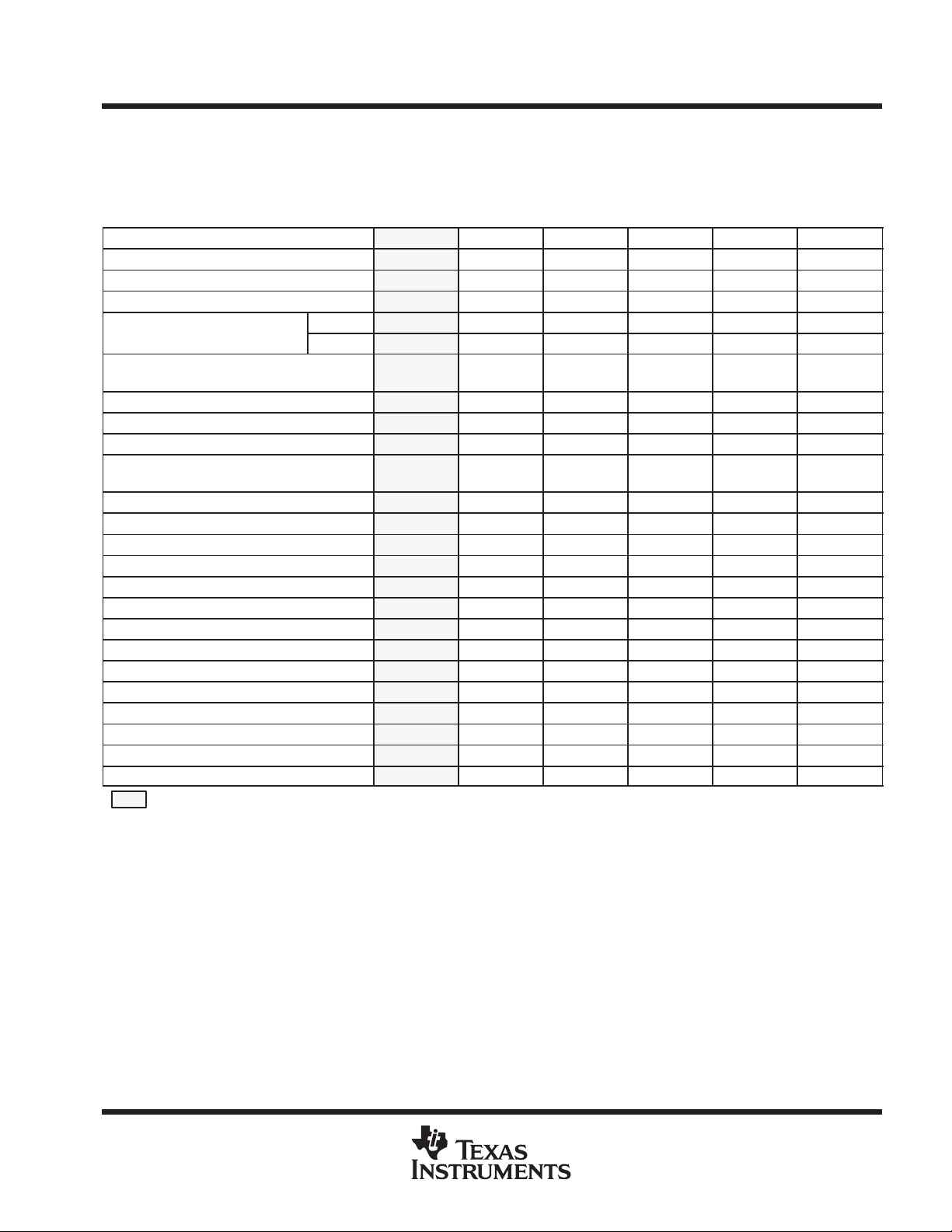
Table 1. Hardware Features of ’240x Devices
FEATURE ’LF2407
’C2xx DSP Core Yes Yes Yes Yes Yes Yes
Instruction Cycle 33 ns 33 ns 33 ns 33 ns 33 ns 33 ns
MIPS (30 MHz) 30 MIPS 30 MIPS 30 MIPS 30 MIPS 30 MIPS 30 MIPS
RAM (16-bit word)
On-chip Flash (16-bit word)
(4 sectors: 4K, 12K, 12K, 4K)
On-chip ROM (16-bit word) — — — 32K 16K 4K
Boot ROM (16-bit word) 256 256 256 — — —
External Memory Interface Yes — — — — —
Event Managers A and B
(EVA and EVB)
S General-Purpose (GP) Timers 4 4 2 4 4 2
S Compare (CMP)/PWM 10/16 10/16 5/8 10/16 10/16 5/8
S Capture (CAP)/QEP 6/4 6/4 3/2 6/4 6/4 3/2
Watchdog Timer Yes Yes Yes Yes Yes Yes
10-Bit ADC Yes Yes Yes Yes Yes Yes
S Channels 16 16 8 16 16 8
S Conversion Time (minimum) 500 ns 500 ns 500 ns 500 ns 500 ns 500 ns
SPI Yes Yes — Yes Yes —
SCI Yes Yes Yes Yes Yes Yes
CAN Yes Yes — Yes — —
Digital I/O Pins (Shared) 41 41 21 41 41 21
External Interrupts 5 5 3 5 5 3
Supply Voltage 3.3 V 3.3 V 3.3 V 3.3 V 3.3 V 3.3 V
Packaging 144 TQFP 100 TQFP 64 PQFP 100 TQFP 100 TQFP 64 PQFP
†
’LF2407, the full-featured device of the ’LF240x family of DSP controllers, is useful for emulation and code development.
DARAM 544 544 544 544 544 544
SARAM 2K 2K — 2K 1K —
EVA, EVB EVA, EVB EVA EVA, EVB EVA, EVB EVA
†
’LF2406 ’LF2402 ’LC2406 ’LC2404 ’LC2402
32K 32K 8K — — —
POST OFFICE BOX 1443 • HOUSTON, TEXAS 77251–1443
3
Page 4
TMS320LF2407, TMS320LF2406, TMS320LF2402
ADVANCE
INFORMATION
TMS320LC2406, TMS320LC2404, TMS320LC2402
DSP CONTROLLERS
SPRS094C – APRIL 1999 – REVISED OCTOBER 1999
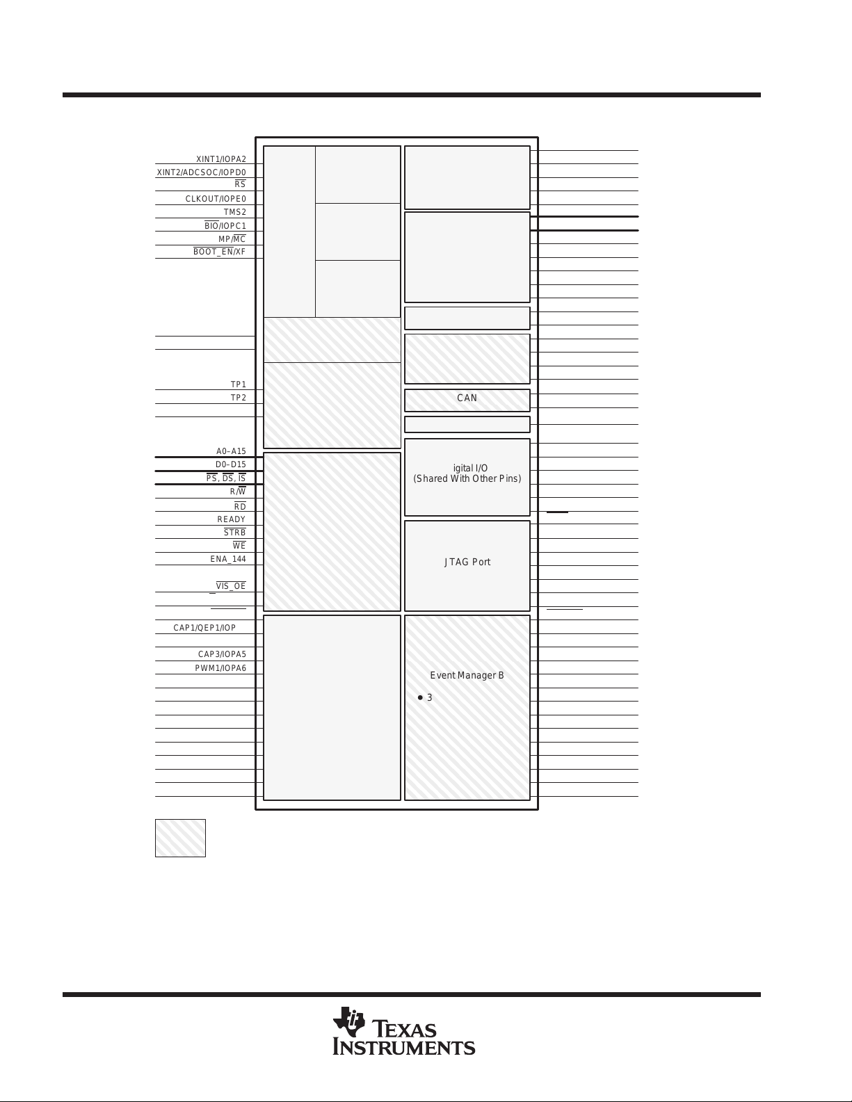
functional block diagram of the ’2407 DSP controller
XINT1/IOPA2
XINT2/ADCSOC/IOPD0
CLKOUT/IOPE0
CAP1/QEP1/IOPA3
CAP2/QEP2/IOPA4
T1PWM/T1CMP/IOPB4
T2PWM/T2CMP/IOPB5
TCLKINA/IOPB7
RS
TMS2
BIO/IOPC1
MP/MC
BOOT_EN/XF
VDD (3.3 V)
V
TP1
TP2
V
(5V)
CCP
A0–A15
D0–D15
PS, DS, IS
R/W
RD
READY
STRB
WE
ENA_144
VIS_OE
W/R / IOPC0
PDPINTA
CAP3/IOPA5
PWM1/IOPA6
PWM2/IOPA7
PWM3/IOPB0
PWM4/IOPB1
PWM5/IOPB2
PWM6/IOPB3
TDIRA/IOPB6
Indicates optional modules
The memory size and peripheral selection of these modules change for different ’240x devices. See
Table 1 for device-specific details.
’C2xx
DSP
Core
SS
SARAM (2K Words)
(32K Words:
4K/12K/12K/4K)
External Memory Interface
Event Manager A
D 3 × Capture Input
D 6 × Compare/PWM
Output
D 2 × GP Timers/PWM
DARAM (B0)
256 Words
DARAM (B1)
256 Words
DARAM (B2)
32 Words
Flash/ROM
PLL Clock
10-Bit ADC
(With Twin
Autosequencer)
SCI
SPI
CAN
WD
Digital I/O
(Shared With Other Pins)
JTAG Port
Event Manager B
D 3 × Capture Input
D 6 × Compare/PWM
Output
D 2 × GP Timers/PWM
PLLF
PLLV
CCA
PLLF2
XTAL1/CLKIN
XTAL2
ADCIN00–ADCIN07
ADCIN08–ADCIN15
V
CCA
V
SSA
V
REFHI
V
REFLO
XINT2/ADCSOC/IOPD0
SCITXD/IOPA0
SCIRXD/IOPA1
SPISIMO/IOPC2
SPISOMI/IOPC3
SPICLK/IOPC4
SPISTE/IOPC5
CANTX/IOPC6
CANRX/IOPC7
V
(5V)
CCP
Port A(0–7) IOPA[0:7]
Port B(0–7) IOPB[0:7]
Port C(0–7) IOPC[0:7]
Port D(0) IOPD[0]
Port E(0–7) IOPE[0:7]
Port F(0–6) IOPF[0:6]
TRST
TDO
TDI
TMS
TCK
EMU0
EMU1
PDPINTB
CAP4/QEP3/IOPE7
CAP5/QEP4/IOPF0
CAP6/IOPF1
PWM7/IOPE1
PWM8/IOPE2
PWM9/IOPE3
PWM10/IOPE4
PWM11/IOPE5
PWM12/IOPE6
T3PWM/T3CMP/IOPF2
T4PWM/T4CMP/IOPF3
TDIRB/IOPF4
TCLKINB/IOPF5
4
POST OFFICE BOX 1443 • HOUSTON, TEXAS 77251–1443
Page 5
TMS320LF2407, TMS320LF2406, TMS320LF2402
ADVANCE
INFORMATION
TMS320LC2406, TMS320LC2404, TMS320LC2402
DSP CONTROLLERS
SPRS094C – APRIL 1999 – REVISED OCTOBER 1999
TDIRB/
T4PWM/T4CMP/
T3PWM/T3CMP/
TDIRA/
T1PWM/T1CMP/
T2PWM/T2CMP/
W/R
XINT2/ADCSOC/
XINT1/
SCITXD/
SCIRXD/
SPISIMO/
SPISOMI/
SPISTE/
SPICLK/
TRST
IOPF4
V
SSO
V
DDO
IOPF3
PDPINTA
IOPF2
PLLF2
PLLF
PLLV
PLLV
CCA
CCA
IOPB6
D10
IOPB4
D11
IOPB5
/IOPC0
D12
IOPD0
D13
IOPA2
D14
IOPA0
IOPA1
D15
V
V
IOPC2
A15
IOPC3
IOPC5
A14
IOPC4
TMS2
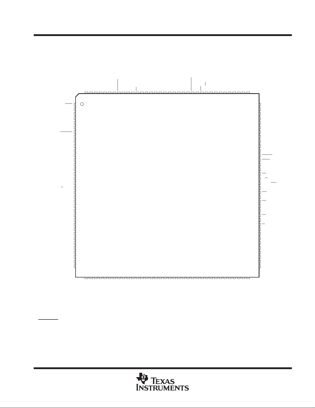
PGE PACKAGE
†
(TOP VIEW)
‡
IOPF5
SS
SSO
DDO
V
PDPINTB
D5
138
A12
D4
137
136
A11
IOPB2
PWM5/
TCK
135
IOPE5
PWM11/
D3
134RS133
A10
IOPB1
PWM4/
TDI
TDO
TMS
D6
V
144
143
142
141
140
139
1
2
3
4
5
D7
6
7
8
9
D8
10
11
12
13
D9
14
15
16
17
18
19
20
21
22
23
24
25
26
27
28
SS
29
DD
30
31
32
33
34
35
36
373839404142434445464748495051525354555657585960616263646566676869
A13
SSO
DDO
V
V
IOPE6
IOPB3
IOPB7
PWM6/
PWM12/
TCLKINA/
DD
D1
D2
V
IOPF6
132
131
130
129
TMS320LF2407
A9
SS
DD
V
V
IOPB0
PWM3/
V
128
A8
D0
TCLKINB/
127
126
IOPE4
IOPA7
PWM2/
PWM10/
SSO
V
125
IOPA6
PWM1/
XTAL1/CLKIN
XTAL2
124
123
A7
CCP
V
BOOT_EN/XF
ENA_144
122
121
TP1
IOPE3
PWM9/
IOPC1
READY
BIO/
119
120
A6
IOPE2
PWM8/
SSA
MP/MC
V
118
117
A5
TP2
CCA
V
116
IOPE1
PWM7/
REFHI
V
115
SSO
V
REFLO
V
114
DDO
V
ADCIN00
ADCIN08
113
112
A4
IOPF1
CAP6/
ADCIN01
ADCIN09
111
110
707172
A3
IOPC7
CANRX/
ADCIN10
109
108
107
106
105
104
103
102
101
100
99
98
97
96
95
94
93
92
91
90
89
88
87
86
85
84
83
82
81
80
79
78
77
76
75
74
73
IOPC6
CANTX/
ADCIN11
ADCIN02
ADCIN12
ADCIN03
ADCIN13
ADCIN04
ADCIN05
ADCIN14
ADCIN06
ADCIN07
ADCIN15
VIS_OE
STRB
V
DDO
V
SSO
RD
R/W
EMU1/OFF
EMU0
WE
CAP4/QEP3/
DS
V
DD
V
SS
PS
CAP1/QEP1/
IS
CAP5/QEP4/
A0
CAP2/QEP2/
A1
V
DDO
V
SSO
CAP3/
IOPA5
A2
/IOPE0
CLKOUT
IOPE7
IOPA3
IOPF0
IOPA4
†
Bold, italicized pin names
‡
BOOT_EN
is available only on flash devices.
indicate pin function after reset.
POST OFFICE BOX 1443 • HOUSTON, TEXAS 77251–1443
5
Page 6
TMS320LF2407, TMS320LF2406, TMS320LF2402
ADVANCE
INFORMATION
TMS320LC2406, TMS320LC2404, TMS320LC2402
DSP CONTROLLERS
SPRS094C – APRIL 1999 – REVISED OCTOBER 1999
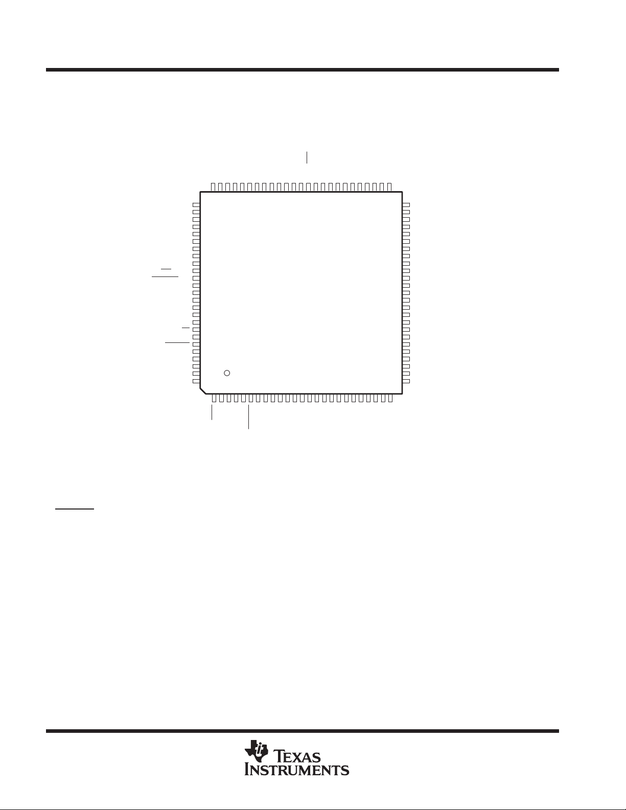
PZ PACKAGE
(TOP VIEW)
DDO
ADCIN06
ADCIN07
ADCIN15
SSO
V
V
ADCIN10
ADCIN01
ADCIN09
ADCIN00
ADCIN08
BIO
BOOT_EN
XTAL1/CLKIN
TCLKINB/
PDPINTB
V
REFLO
V
REFHI
V
V
/IOPC1
/XF
XTAL2
IOPF5
V
IOPF6
TCK
V
V
TDO
TMS
CCA
SSA
V
RS
TDI
SSO
DDO
ADCIN11
ADCIN02
ADCIN12
ADCIN03
ADCIN13
ADCIN04
ADCIN05
ADCIN14
76
77
78
79
80
81
82
83
84
85
§
86
87
88
89
90
SS
DD
91
92
93
94
95
96
97
98
99
TMS320LC2404
TMS320LC2406
TMS320LF2406
†
IOPE7
OFF
DD
SS
EMU1/
EMU0
CAP4/QEP3/VCAP1/QEP1/
V
IOPA4
IOPF0
IOPA3
CAP5/QEP4/
CAP2/QEP2/VCAP3/
DDO
V
SSO
/IOPE0
IOPA5
CLKOUT
51525354555657585960616263646566676869707172737475
50
49
48
47
46
45
44
43
42
41
40
39
38
37
36
35
34
33
32
31
30
29
28
27
26100
25242322212019181716151413121110987654321
CANTX/
CANRX/
CAP6/
IOPF1
V
DDO
V
SSO
PWM7/
TP2
PWM8/
TP1
PWM9/
V
CCP
PWM1/
PWM10/
PWM2/
PWM3/
V
DD
V
SS
PWM4/
PWM11/
PWM5/
V
DDO
V
SSO
PWM6/
PWM12/
TCLKINA/
IOPC6
IOPC7
IOPE1
IOPE2
IOPE3
IOPA6
IOPE4
IOPA7
IOPB0
IOPB1
IOPE5
IOPB2
IOPB3
IOPE6
IOPB7
‡
‡
†
Bold, italicized pin names
‡
CANTX and CANRX are not available on ’LC2404 devices.
§
BOOT_EN
indicate pin function after reset.
is available only on flash devices.
TRST
SSOVSSO
V
IOPF4
IOPF4
TDIRB/
TDIRB/
DDO
IOPF2
IOPF3
V
PDPINTA
T3PWM/T3CMP/
T4PWM/T4CMP/
PLLF
PLLF2
CCA
IOPB4
IOPB6
PLLV
TDIRA/
T1PWM/T1CMP/
IOPA0
IOPA2
IOPB5
IOPC0
IOPD0
XINT1/
SCITXD/
T2PWM/T2CMP/
XINT2/ADCSOC/
SS
DD
V
V
IOPA1
SCIRXD/
IOPC3
IOPC2
IOPC5
SPISTE/
SPISIMO/
SPISOMI/
TMS2
IOPC4
SPICLK/
6
POST OFFICE BOX 1443 • HOUSTON, TEXAS 77251–1443
Page 7
TMS320LF2407, TMS320LF2406, TMS320LF2402
ADVANCE
INFORMATION
TMS320LC2406, TMS320LC2404, TMS320LC2402
DSP CONTROLLERS
SPRS094C – APRIL 1999 – REVISED OCTOBER 1999
V
DDO
PWM5
PWM4
V
SS
V
DD
PWM3
PWM2
PWM1
V
CCP
TP1
TP2
IOPC7
IOPC6
52
53
54
55
56
57
58
59
60
61
62
63
64
SSO
V
IOPB7
IOPB3
TCLKINA/
PWM6/
TMS2
IOPC4
PG PACKAGE
(TOP VIEW)
IOPA1
IOPA0
SCIRXD/
SCITXD/
IOPC2
IOPC3
TMS320LC2402
TMS320LF2402
†
IOPD0
IOPB4
IOPB5
CCA
T1PWM/T1CMP/
T2PWM/T2CMP/
XINT2/ADCSOC/
PLLV
PLLF
PDPINTA
PLLF2
DDO
V
SSO
V
3351 343550 49 48 47 46 45 44 43 42 41 40 3938 37 36
191 2 3 4 5 6 7 8 9101112131415161718
TRST
32
31
30
29
28
27
26
25
24
23
22
21
20
TMS
TDO
TDI
TCK
RS
V
DD
V
SS
XTAL2
XTAL1/CLKIN
BOOT_EN
V
SSA
V
CCA
V
REFHI
/XF
‡
†
Bold, italicized pin names
‡
BOOT_EN
is available only on flash devices.
SS
VDDV
IOPA3
IOPA4
IOPA5
/IOPE0
CAP3/
CLKOUT
CAP1/QEP1/
CAP2/QEP2/
indicate pin function after reset.
OFF
EMU0
EMU1/
SSO
V
DDO
V
ADCIN07
ADCIN04
ADCIN05
ADCIN06
ADCIN01
ADCIN02
ADCIN03
REFLO
V
ADCIN00
POST OFFICE BOX 1443 • HOUSTON, TEXAS 77251–1443
7
Page 8
TMS320LF2407, TMS320LF2406, TMS320LF2402
ADVANCE
INFORMATION
TMS320LC2406, TMS320LC2404, TMS320LC2402
DSP CONTROLLERS
SPRS094C – APRIL 1999 – REVISED OCTOBER 1999
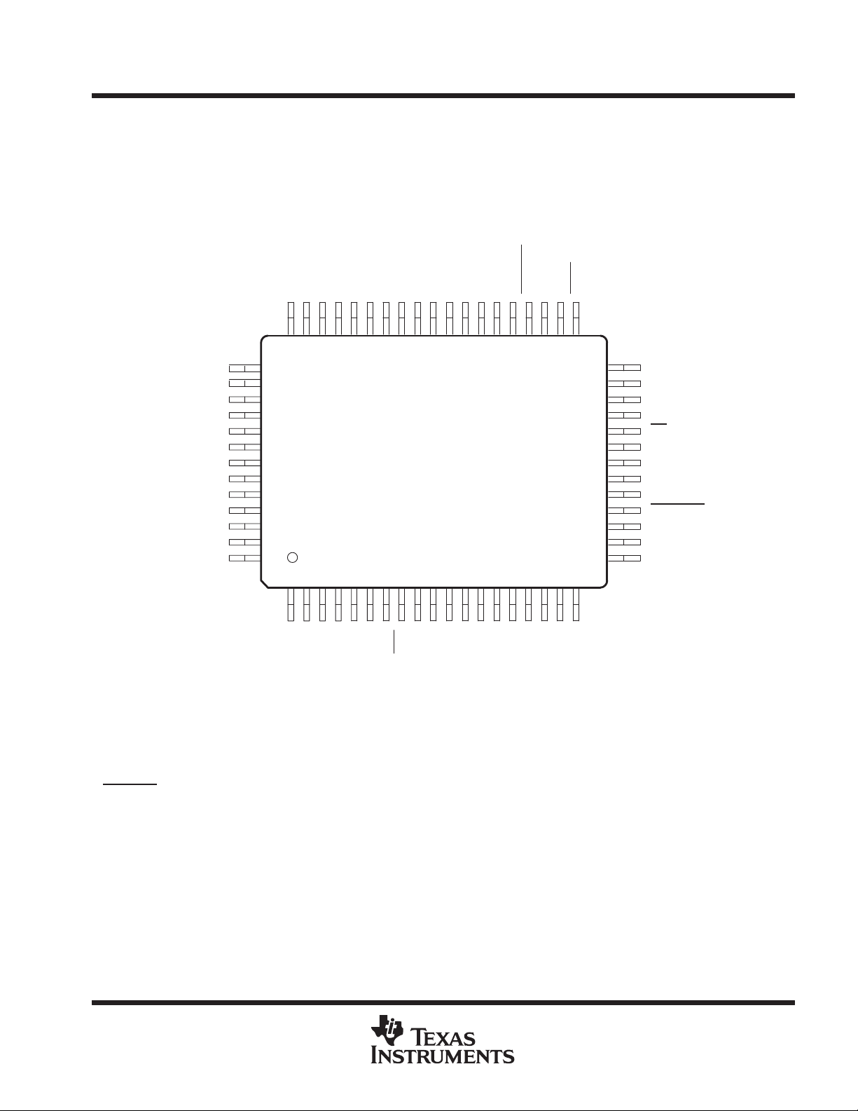
pin functions
The TMS320LF2407 device is the superset of all the ’240x devices. All signals are available on the ’2407 device.
Table 2 lists the key signals available in the ’240x family of devices.
CAP1/QEP1/
CAP2/QEP2/
CAP3/
PWM1/
PWM2/
PWM3/
PWM4/
PWM5/
PWM6/
T1PWM/T1CMP/
T2PWM/T2CMP/
TDIRA/
TCLKINA/
CAP4/QEP3/
CAP5/QEP4/
CAP6/
PWM7/
PWM8/
PWM9/
PWM10/
PWM11/
PWM12/
T3PWM/T3CMP/
T4PWM/T4CMP/
TDIRB/
TCLKINB/
†
Bold, italicized pin names
‡
GPIO – General-purpose input/output pin. All GPIOs come up as input after reset.
§
Pin changes with respect to SPRS094B data sheet.
LEGEND: ↑ – Internal pullup ↓ – Internal pulldown
Table 2. ’LF240x and ’LC240x Pin List and Package Options
PIN NAME ’LF2407 ’2406 ’LC2404 ’2402 DESCRIPTION
EVENT MANAGER A (EVA)
Capture input #1/quadrature encoder pulse input #1 (EVA) or
GPIO (↑)
Capture input #2/quadrature encoder pulse input #2 (EVA) or
GPIO (↑)
§
Compare/PWM output pin #1 (EVA) or GPIO (↑)
§
Compare/PWM output pin #2 (EVA) or GPIO (↑)
§
Compare/PWM output pin #3 (EVA) or GPIO (↑)
§
Compare/PWM output pin #4 (EVA) or GPIO (↑)
§
Compare/PWM output pin #5 (EVA) or GPIO (↑)
Counting direction for general-purpose (GP) timer (EVA) or
GPIO. If TDIRA=1, upward counting is selected. If TDIRA=0,
downward counting is selected. (↑)
External clock input for GP timer (EVA) or GPIO. Note that timer
can also use the internal device clock. (↑)
Capture input #4/quadrature encoder pulse input #3 (EVB) or
GPIO (↑)
Capture input #5/quadrature encoder pulse input #4 (EVB) or
GPIO (↑)
Counting direction for general-purpose (GP) timer (EVB) or
GPIO. If TDIRB=1, upward counting is selected. If TDIRB=0,
downward counting is selected. (↑)
External clock input for GP timer (EVB) or GPIO. Note that timer
can also use the internal device clock. (↑)
IOPA5
IOPA6
IOPA7
IOPB0
IOPB1
IOPB2
IOPB3
IOPB6
IOPB7
IOPF1
IOPE1
IOPE2
IOPE3
IOPE4
IOPE5
IOPE6
IOPF4
IOPF5
IOPA3
IOPA4
IOPB4
IOPB5
IOPE7
IOPF0
IOPF2
IOPF3
83 57 57 4
79 55 55 3
75 52 52 2 Capture input #3 (EVA) or GPIO (↑)
56 39 39 59
54 37 37 58
52 36 36 57
47 33 33 54
44 31 31 53
40 28 28 50 Compare/PWM output pin #6 (EVA) or GPIO (↑)
16 12 12 40 Timer 1 compare output (EVA) or GPIO (↑)
18 13 13 41 Timer 2 compare output (EVA) or GPIO (↑)
14 11 11
37 26 26 49
EVENT MANAGER B (EVB)
88 60 60
81 56 56
69 48 48 Capture input #6 (EVB) or GPIO (↑)
65 45 45 Compare/PWM output pin #7 (EVB) or GPIO (↑)
62 43 43 Compare/PWM output pin #8 (EVB) or GPIO (↑)
59 41 41 Compare/PWM output pin #9 (EVB) or GPIO (↑)
55 38 38 Compare/PWM output pin #10 (EVB) or GPIO (↑)
46 32 32 Compare/PWM output pin #11 (EVB) or GPIO (↑)
38 27 27 Compare/PWM output pin #12 (EVB) or GPIO (↑)
8 7 7 Timer 3 compare output (EVB) or GPIO (↑)
6 5 5 Timer 4 compare output (EVB) or GPIO (↑)
2 2 2
126 89 89
indicate pin function after reset.
†‡
8
POST OFFICE BOX 1443 • HOUSTON, TEXAS 77251–1443
Page 9
ADVANCE
INFORMATION
TMS320LF2407, TMS320LF2406, TMS320LF2402
TMS320LC2406, TMS320LC2404, TMS320LC2402
DSP CONTROLLERS
SPRS094C – APRIL 1999 – REVISED OCTOBER 1999
pin functions (continued)
Table 2. ’LF240x and ’LC240x Pin List and Package Options†‡ (Continued)
PIN NAME ’LF2407 ’2406 ’LC2404 ’2402 DESCRIPTION
ANALOG-TO-DIGITAL CONVERTER (ADC)
ADCIN00 112 79 79 18 Analog input #0 to the ADC
ADCIN01 110 77 77 17 Analog input #1 to the ADC
ADCIN02 107 74 74 16 Analog input #2 to the ADC
ADCIN03 105 72 72 15 Analog input #3 to the ADC
ADCIN04 103 70 70 14 Analog input #4 to the ADC
ADCIN05 102 69 69 13 Analog input #5 to the ADC
ADCIN06 100 67 67 12 Analog input #6 to the ADC
ADCIN07 99 66 66 11 Analog input #7 to the ADC
ADCIN08 113 80 80 Analog input #8 to the ADC
ADCIN09 111 78 78 Analog input #9 to the ADC
ADCIN10 109 76 76 Analog input #10 to the ADC
ADCIN11 108 75 75 Analog input #11 to the ADC
ADCIN12 106 73 73 Analog input #12 to the ADC
ADCIN13 104 71 71 Analog input #13 to the ADC
ADCIN14 101 68 68 Analog input #14 to the ADC
ADCIN15 98 65 65 Analog input #15 to the ADC
V
REFHI
V
REFLO
V
CCA
V
SSA
CONTROLLER AREA NETWORK (CAN), SERIAL COMMUNICATIONS INTERFACE (SCI), SERIAL PERIPHERAL INTERFACE (SPI)
CANRX/
CANTX/
SCITXD/
SCIRXD/
SPICLK/
SPISIMO/
SPISOMI/
SPISTE/
†
‡
IOPC7
IOPC6
IOPA0
IOPA1
IOPC4
IOPC2
IOPC3
IOPC5
Bold, italicized pin names
GPIO – General-purpose input/output pin. All GPIOs come up as input after reset.
LEGEND: ↑ – Internal pullup ↓ – Internal pulldown
CANRX 70 49 – –
IOPC7 70 49 49 63
CANTX 72 50 – –
IOPC6 72 50 50 64
SPICLK 35 24 24 –
IOPC4 35 24 24 47
SPISIMO 30 21 21 –
IOPC2 30 21 21 45
SPISOMI 32 22 22 –
IOPC3 32 22 22 46
SPISTE 33 23 23 –
IOPC5 33 23 23 –
indicate pin function after reset.
115 82 82 20 ADC analog high-voltage reference input
114 81 81 19 ADC analog low-voltage reference input
116 83 83 21
117 84 84 22 Analog ground reference for ADC
25 17 17 43
26 18 18 44
Analog supply voltage for ADC (3.3 V). V
be isolated from digital supply voltage.
CAN receive data or GPIO (↑)
CAN transmit data or GPIO (↑)
SCI asynchronous serial port transmit data or
GPIO (↑)
SCI asynchronous serial port receive data or or
GPIO (↑)
SPI clock or GPIO (↑)
SPI slave in, master out or GPIO (↑)
SPI slave out, master in or GPIO (↑)
SPI slave transmit enable (optional) or GPIO (↑)
CCA
must
POST OFFICE BOX 1443 • HOUSTON, TEXAS 77251–1443
9
Page 10
TMS320LF2407, TMS320LF2406, TMS320LF2402
ADVANCE
INFORMATION
TMS320LC2406, TMS320LC2404, TMS320LC2402
DSP CONTROLLERS
SPRS094C – APRIL 1999 – REVISED OCTOBER 1999
pin functions (continued)
RS 133 93 93 28
PDPINTA 7 6 6 36
XINT1/
XINT2/ADCSOC/
CLKOUT
PDPINTB 137 95 95
XTAL1/CLKIN 123 87 87 24
XTAL2 124 88 88 25
PLLF 11 9 9 38 Filter input 1
PLLV
PLLF2 10 8 8 37 Filter input 2
BOOT_EN / XF
†
Bold, italicized pin names
‡
GPIO – General-purpose input/output pin. All GPIOs come up as input after reset.
LEGEND: ↑ – Internal pullup ↓ – Internal pulldown
Table 2. ’LF240x and ’LC240x Pin List and Package Options†‡ (Continued)
PIN NAME ’LF2407 ’2406 ’LC2404 ’2402 DESCRIPTION
EXTERNAL INTERRUPTS, CLOCK
Device reset. RS causes the ’240x to terminate
execution and sets PC = 0. When RS
high level, execution begins at location zero of
program memory. RS
registers and status bits. When the watchdog timer
overflows, it initiates a system reset pulse that is
reflected on the RS
Power drive protection interrupt input. This interrupt,
when activated, puts the PWM output pins (EVA) in the
high-impedance state should motor drive/power
converter abnormalities, such as overvoltage or
overcurrent, etc., arise. PDPINTA
falling-edge-sensitive interrupt. (↑)
External user interrupt 1 or GPIO. Both XINT1 and
IOPA2
IOPD0
/IOPE0 73 51 51 1
CCA
BOOT_EN 121 86 – 23
XF 121 86 86 23
indicate pin function after reset.
23 16 16
21 15 15 42
OSCILLATOR, PLL, FLASH, BOOT, AND MISCELLANEOUS
12 10 10 39 PLL supply (3.3 V)
XINT2 are edge-sensitive. The edge polarity is
programmable. (↑)
External user interrupt 2 and ADC start of conversion
or GPIO. External “start-of-conversion” input for
ADC/GPIO. Both XINT1 and XINT2 are
edge-sensitive. The edge polarity is
programmable. (↑)
Clock output or GPIO. This pin outputs either the CPU
clock (CLKOUT) or the watchdog clock (WDCLK). The
selection is made by the CLKSRC bit (bit 14) of the
System Control and Status Register (SCSR). This pin
can be used as a GPIO if not used as a clock output
pin. (↑)
Power drive protection interrupt input. This interrupt,
when activated, puts the PWM output pins (EVB) in
the high-impedance state should motor drive/power
converter abnormalities, such as overvoltage or
overcurrent, etc., arise. PDPINT
falling-edge-sensitive interrupt. (↑)
PLL oscillator input pin. Crystal input to PLL/clock
source input to PLL. XTAL1/CLKIN is tied to one side
of a reference crystal.
Crystal output. PLL oscillator output pin. XTAL2 is tied
to one side of a reference crystal. This pin goes in the
high-impedance state when EMU1/OFF
Boot ROM enable, GPO, XF. This pin will be sampled
as input (BOOT_EN
bit) during reset and then driven as an output signal for
XF. ROM devices do not have boot ROM, hence, no
BOOT_EN modes. (↑)
is brought to a
affects (or sets to zero) various
pin. (↑)
is a
is a
is active low.
) to update SCSR2.3 (BOOT_EN
10
POST OFFICE BOX 1443 • HOUSTON, TEXAS 77251–1443
Page 11
ADVANCE
INFORMATION
TMS320LF2407, TMS320LF2406, TMS320LF2402
TMS320LC2406, TMS320LC2404, TMS320LC2402
DSP CONTROLLERS
SPRS094C – APRIL 1999 – REVISED OCTOBER 1999
pin functions (continued)
Table 2. ’LF240x and ’LC240x Pin List and Package Options†‡ (Continued)
PIN NAME ’LF2407 ’2406 ’LC2404 ’2402 DESCRIPTION
OSCILLATOR, PLL, FLASH, BOOT, AND MISCELLANEOUS (CONTINUED)
Flash programming voltage pin. This is the 5-V supply used for
flash programming. Flash cannot be programmed if this pin is
V
(5V) 58 40 40 60
CCP
TP1 (Flash) 60 42 42 61
TP2 (Flash) 63 44 44 62
IOPF6 131 92 92 General-purpose I/O (↑)
BIO
/IOPC1 119 85 85
EMULATION AND TEST
EMU0 90 61 61 7
EMU1/OFF 91 62 62 8
TCK 135 94 94 29 JTAG test clock with internal pullup (↑)
TDI 139 96 96 30
TDO 142 99 99 31
TMS 144 100 100 32
TMS2 36 25 25 48
TRST 1 1 1 33
†
Bold, italicized pin names
‡
GPIO – General-purpose input/output pin. All GPIOs come up as input after reset.
§
Pin changes with respect to SPRS094B data sheet.
LEGEND: ↑ – Internal pullup ↓ – Internal pulldown
indicate pin function after reset.
§
held at 0 V . Connect to 5-V supply for programming or tie it to
GND during functional mode.
§
Flash array test pin.
§
Flash array test pin
Branch control input. BIO is polled by the BCND pma,BIO
instruction. If BIO
used, it should be pulled high. This pin is configured as a branch
control input by all device resets. It can be used as a GPIO, if
not used as a branch control input. (↑)
Emulator I/O #0 with internal pullup. When TRST is driven high,
this pin is used as an interrupt to or from the emulator system
and is defined as input/output through the JTAG scan. (↑)
Emulator pin 1. Emulator pin 1 disables all outputs. When TRST
is driven high, EMU1/OFF is used as an interrupt to or from the
emulator system and is defined as an input/output through the
JTAG scan. When TRST
OFF
. EMU1/OFF, when active low, puts all output drivers in the
high-impedance state. Note that OFF
testing and emulation purposes (not for multiprocessing
applications). Therefore, for the OFF
apply:
= 0
TRST
EMU0 = 1
EMU1/OFF
JTAG test data input (TDI) with internal pullup. TDI is clocked
into the selected register (instruction or data) on a rising edge of
TCK. (↑)
JTAG scan out, test data output (TDO). The contents of the
selected register (instruction or data) is shifted out of TDO on
the falling edge of TCK. (↓)
JTAG test-mode select (TMS) with internal pullup. This serial
control input is clocked into the TAP controller on the rising edge
of TCK. (↑)
JTAG test-mode select 2 (TMS) with internal pullup. This serial
control input is clocked into the TAP controller on the rising edge
of TCK. Used for test and emulation only. (↑)
JTAG test reset with internal pulldown. TRST, when driven high,
gives the scan system control of the operations of the device. If
this signal is not connected or driven low, the device operates in
its functional mode, and the test reset signals are ignored. (↓)
= 0
Do not connect.
. Do not connect.
is low, a branch is executed. If BIO is not
is driven low, this pin is configured as
is used exclusively for
condition, the following
POST OFFICE BOX 1443 • HOUSTON, TEXAS 77251–1443
11
Page 12
TMS320LF2407, TMS320LF2406, TMS320LF2402
ADVANCE
INFORMATION
TMS320LC2406, TMS320LC2404, TMS320LC2402
DSP CONTROLLERS
SPRS094C – APRIL 1999 – REVISED OCTOBER 1999
pin functions (continued)
DS 87
IS 82
PS 84
R/W 92
W/R
RD 93
WE 89
STRB 96
READY 120
†
Bold, italicized pin names
‡
GPIO – General-purpose input/output pin. All GPIOs come up as input after reset.
LEGEND: ↑ – Internal pullup ↓ – Internal pulldown
Table 2. ’LF240x and ’LC240x Pin List and Package Options†‡ (Continued)
PIN NAME ’LF2407 ’2406 ’LC2404 ’2402 DESCRIPTION
ADDRESS, DATA, AND MEMORY CONTROL SIGNALS
Data space strobe. IS, DS, and PS are always high
unless low-level asserted for access to the relevant
external memory space or I/O. They are placed in the
high-impedance state during reset, power down, and
when EMU1/OFF
I/O space strobe. IS, DS, and PS are always high
unless low-level asserted for access to the relevant
external memory space or I/O. They are placed in the
high-impedance state during reset, power down, and
when EMU1/OFF
Program space strobe. IS, DS, and PS are always
high unless low-level asserted for access to the
relevant external memory space or I/O. They are
placed in the high-impedance state during reset,
power down, and when EMU1/OFF
Read/write qualifier signal. R/W indicates transfer
direction during communication to an external device.
It is normally in read mode (high), unless low level is
asserted for performing a write operation. It is placed
in the high-impedance state when EMU1/OFF
active low and during power down.
Write/Read qualifier or GPIO. This is an inverted R/W
signal useful for zero-wait-state memory interface. It
is normally low, unless a memory write operation is
performed. See T able 13, Port C section, for reset
note regarding ’LF2406 and ’LF2402. (↑)
Read enable strobe. Read-select indicates an active,
external read cycle. RD
program, data, and I/O reads. RD
high-impedance state when EMU1/OFF
Write enable strobe. The falling edge of WE indicates
that the device is driving the external data bus
(D15–D0). WE
data, and I/O writes. WE
state when EMU1/OFF
External memory access strobe. STRB is always high
unless asserted low to indicate an external bus cycle.
is active for all off-chip accesses. It is placed in
STRB
the high-impedance state during power down, and
when EMU1/OFF
READY is pulled low to add wait states for external
accesses. READY indicates that an external device is
prepared for a bus transaction to be completed. If the
device is not ready, it pulls the READY pin low. The
processor waits one cycle and checks READY again.
Note that the processor performs READY-detection if
at least one software wait state is programmed. To
meet the external READY timings, the wait-state
generator control register (WSGR) should be
programmed for at least one wait state. (↑)
is active on all external program,
/ IOPC0
W/R
IOPC0 19 14 14
indicate pin function after reset.
19
is active low.
is active low.
is active low.
is
is active on all external
goes into the
is active low.
goes in the high-impedance
is active low.
is active low.
12
POST OFFICE BOX 1443 • HOUSTON, TEXAS 77251–1443
Page 13
ADVANCE
INFORMATION
TMS320LF2407, TMS320LF2406, TMS320LF2402
TMS320LC2406, TMS320LC2404, TMS320LC2402
SPRS094C – APRIL 1999 – REVISED OCTOBER 1999
pin functions (continued)
Table 2. ’LF240x and ’LC240x Pin List and Package Options†‡ (Continued)
PIN NAME ’LF2407 ’2406 ’LC2404 ’2402 DESCRIPTION
ADDRESS, DATA, AND MEMORY CONTROL SIGNALS (CONTINUED)
Microprocessor/Microcomputer mode select. If this pin is low
during reset, the device is put in microcomputer mode and
program execution begins at 0000h of internal program memory
MP/MC 118
ENA_144 122
VIS_OE 97
A0 80 Bit 0 of the 16-bit address bus
A1 78 Bit 1 of the 16-bit address bus
A2 74 Bit 2 of the 16-bit address bus
A3 71 Bit 3 of the 16-bit address bus
A4 68 Bit 4 of the 16-bit address bus
A5 64 Bit 5 of the 16-bit address bus
A6 61 Bit 6 of the 16-bit address bus
A7 57 Bit 7 of the 16-bit address bus
A8 53 Bit 8 of the 16-bit address bus
A9 51 Bit 9 of the 16-bit address bus
A10 48 Bit 10 of the 16-bit address bus
A11 45 Bit 11 of the 16-bit address bus
A12 43 Bit 12 of the 16-bit address bus
A13 39 Bit 13 of the 16-bit address bus
A14 34 Bit 14 of the 16-bit address bus
A15 31 Bit 15 of the 16-bit address bus
D0 127 Bit 0 of 16-bit data bus (↑)
D1 130 Bit 1 of 16-bit data bus (↑)
D2 132 Bit 2 of 16-bit data bus (↑)
D3 134 Bit 3 of 16-bit data bus (↑)
D4 136 Bit 4 of 16-bit data bus (↑)
D5 138 Bit 5 of 16-bit data bus (↑)
D6 143 Bit 6 of 16-bit data bus (↑)
D7 5 Bit 7 of 16-bit data bus (↑)
D8 9 Bit 8 of 16-bit data bus (↑)
†
Bold, italicized pin names
‡
GPIO – General-purpose input/output pin. All GPIOs come up as input after reset.
LEGEND: ↑ – Internal pullup ↓ – Internal pulldown
indicate pin function after reset.
(flash EEPROM). A high value during reset puts the device in
microprocessor mode and program execution begins at 0000h of
external program memory. This line sets the MP/MC
the SCSR2 register). (↓)
Active high to enable external interface signals. If pulled low, the
’2407 behaves like the ’2406/’2404—i.e., it has no external
memory and generates an illegal address if any of the three
external spaces are accessed (IS
has an internal pulldown. (↓)
Visibility output enable (active when data bus is output). This pin
is active (low) whenever the external databus is driving as an
output during visibility mode. Can be used by external decode
logic to prevent data bus contention while running in visibility
mode.
DSP CONTROLLERS
bit (bit 2 in
and DS asserted). This pin
POST OFFICE BOX 1443 • HOUSTON, TEXAS 77251–1443
13
Page 14
TMS320LF2407, TMS320LF2406, TMS320LF2402
V
SSO
I/O buffer ground. Digital logic and buffer ground reference.
ADVANCE
INFORMATION
TMS320LC2406, TMS320LC2404, TMS320LC2402
DSP CONTROLLERS
SPRS094C – APRIL 1999 – REVISED OCTOBER 1999
pin functions (continued)
D9 13 Bit 9 of 16-bit data bus (↑)
D10 15 Bit 10 of 16-bit data bus (↑)
D11 17 Bit 11 of 16-bit data bus (↑)
D12 20 Bit 12 of 16-bit data bus (↑)
D13 22 Bit 13 of 16-bit data bus (↑)
D14 24 Bit 14 of 16-bit data bus (↑)
D15 27 Bit 15 of 16-bit data bus (↑)
V
DD
V
DDO
V
SS
V
SSO
†
Bold, italicized pin names
‡
GPIO – General-purpose input/output pin. All GPIOs come up as input after reset.
§
Pin changes with respect to SPRS094B data sheet.
LEGEND: ↑ – Internal pullup ↓ – Internal pulldown
Table 2. ’LF240x and ’LC240x Pin List and Package Options†‡ (Continued)
PIN NAME ’LF2407 ’2406 ’LC2404 ’2402 DESCRIPTION
ADDRESS, DATA, AND MEMORY CONTROL SIGNALS (CONTINUED)
POWER SUPPLY
29 20 20 6
50 35 35 27
86 59 59 56
129 91 91
4 4 4 10
42 30 30 35
67 47 47 52
77 54 54
95 64 64
141 98 98
28 19 19 5
49 34 34 26
85 58 58 55
128 90 90
3 3 3 9
41 29 29 34
66 46 46 51
76 53 53
94 63 63
125 97 97
140
indicate pin function after reset.
Core supply +3.3 V . Digital logic supply voltage.
§
§
I/O buffer supply +3.3 V. Digital logic and buffer supply voltage.
Core ground. Digital logic ground reference.
§
§
I/O buffer ground. Digital logic and buffer ground reference.
14
POST OFFICE BOX 1443 • HOUSTON, TEXAS 77251–1443
Page 15
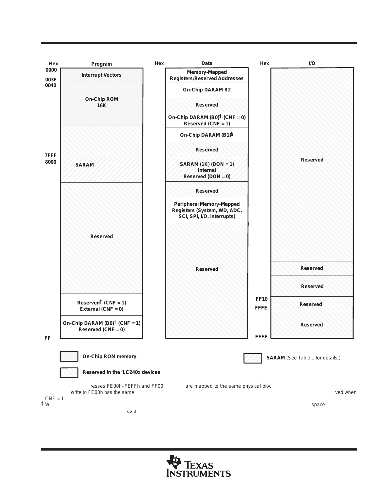
memory maps – ’LF2407
ADVANCE
INFORMATION
TMS320LF2407, TMS320LF2406, TMS320LF2402
TMS320LC2406, TMS320LC2404, TMS320LC2402
DSP CONTROLLERS
SPRS094C – APRIL 1999 – REVISED OCTOBER 1999
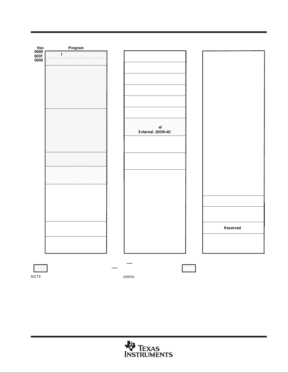
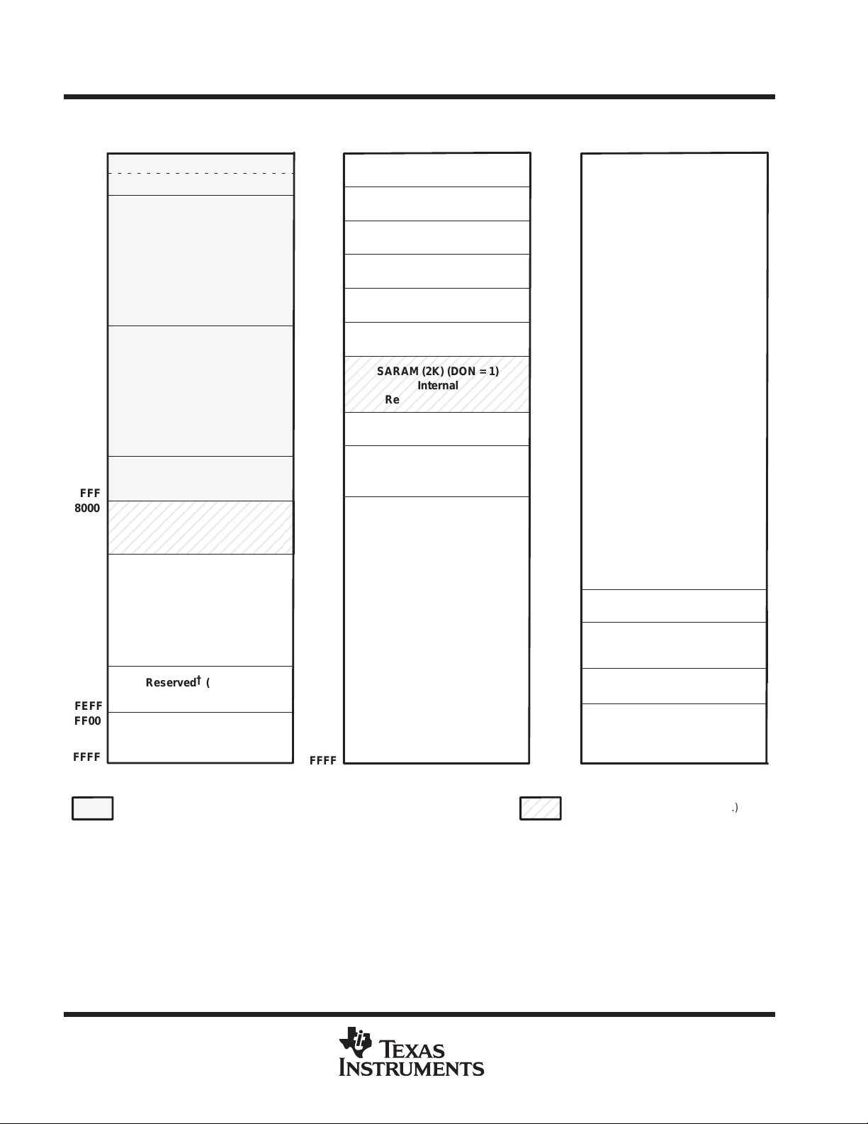
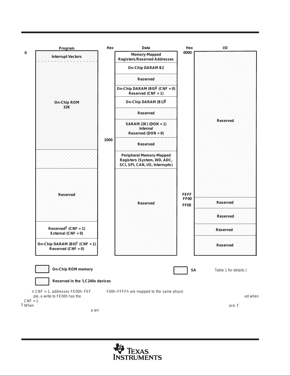
Hex Program
0000
003F
0040
0FFF
1000
3FFF
4000
6FFF
7000
7FFF
8000
87FF
8800
FDFF
FE00
FEFF
FF00
On-Chip DARAM (B0)† (CNF = 1)
FFFF
Interrupt Vectors
FLASH SECTOR 0 (4K)
FLASH SECTOR 1 (12K)
FLASH SECTOR 2 (12K)
FLASH SECTOR 3 (4K)
SARAM (2K) (PON = 1)
Internal
External (PON=0)
External
Reserved† (CNF = 1)
External (CNF = 0)
External (CNF = 0)
Hex Data
0000
005F
0060
007F
0080
01FF
0200
On-Chip DARAM (B0)‡ (CNF = 0)
02FF
0300
03FF
0400
07FF
0800
0FFF
1000
6FFF
7000
7FFF
8000
FFFF
Memory-Mapped
Registers/Reserved Addresses
On-Chip DARAM B2
Reserved
Reserved (CNF = 1)
On-Chip DARAM (B1)
Reserved
SARAM (2K) (DON = 1)
Internal
External (DON=0)
Reserved
Peripheral Memory-Mapped
Registers (System, WD, ADC,
SCI, SPI, CAN, I/O, Interrupts)
External
Hex I/O
0000
§
External
FEFF
FF00
FF0E
FF0F
FF10
FFFE
FFFF
Reserved
Flash Control Mode Register
(Only for Flash Devices)
Reserved
Wait-State Generator Control
Register (On-Chip)
On-Chip Flash Memory (Sectored) – if MP/MC = 0
External Program Memory – if MP/MC
NOTE A: Boot ROM: If the boot ROM is enabled, then address 0000–00FF in the program space will be occupied by boot ROM.
†
When CNF = 1, addresses FE00h–FEFFh and FF00h–FFFFh are mapped to the same physical block (B0) in program-memory space. For
example, a write to FE00h has the same effect as a write to FF00h. For simplicity, addresses FE00h–FEFFh are referred to as reserved when
CNF = 1.
‡
When CNF = 0, addresses 0100h–01FFh and 0200h–02FFh are mapped to the same physical block (B0) in data-memory space. For example,
a write to 0100h has the same effect as a write to 0200h. For simplicity , addresses 0100h–01FFh are referred to as reserved.
§
Addresses 0300h–03FFh and 0400h–04FFh are mapped to the same physical block (B1) in data-memory space. For example, a write to 0400h
has the same effect as a write to 0300h. For simplicity , addresses 0400h–04FFh are referred to as reserved.
= 1
SARAM (See Table 1 for details.)
Figure 1. TMS320LF2407 Memory Map
POST OFFICE BOX 1443 • HOUSTON, TEXAS 77251–1443
15
Page 16
TMS320LF2407, TMS320LF2406, TMS320LF2402
ADVANCE
INFORMATION
TMS320LC2406, TMS320LC2404, TMS320LC2402
DSP CONTROLLERS
SPRS094C – APRIL 1999 – REVISED OCTOBER 1999
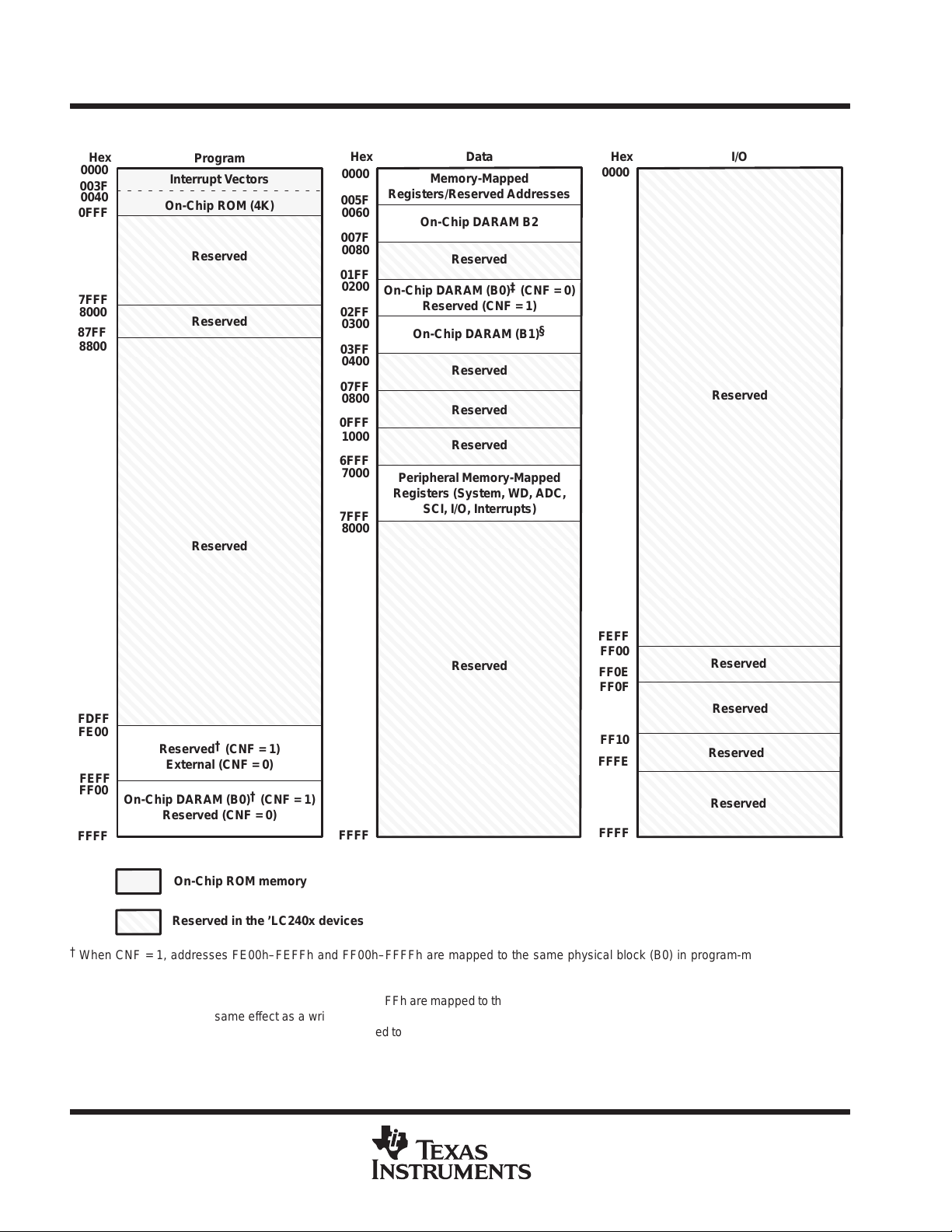
memory maps (continued) – ’LF2406
Hex Program
0000
003F
0040
0FFF
1000
3FFF
4000
6FFF
7000
7FFF
8000
87FF
8800
FDFF
FE00
FEFF
FF00
FFFF
Interrupt Vectors
FLASH SECTOR 0 (4K)
FLASH SECTOR 1 (12K)
FLASH SECTOR 2 (12K)
FLASH SECTOR 3 (4K)
SARAM (2K) (PON = 1)
Internal
External (PON=0)
Reserved
Reserved† (CNF = 1)
External (CNF = 0)
On-Chip DARAM (B0)† (CNF = 1)
External (CNF = 0)
Hex Data
0000
005F
0060
007F
0080
01FF
0200
02FF
0300
03FF
0400
07FF
0800
0FFF
1000
6FFF
7000
7FFF
8000
FFFF
Memory-Mapped
Registers/Reserved Addresses
On-Chip DARAM B2
Reserved
On-Chip DARAM (B0)‡ (CNF = 0)
Reserved (CNF = 1)
On-Chip DARAM (B1)
Reserved
SARAM (2K) (DON = 1)
Internal
Reserved (DON = 0)
Reserved
Peripheral Memory-Mapped
Registers (System, WD, ADC,
SCI, SPI, CAN, I/O, Interrupts)
Reserved
Hex I/O
0000
§
Reserved
FEFF
FF00
FF0E
FF0F
FF10
FFFE
FFFF
Flash Control Mode Register
Reserved
(Only for Flash devices)
Reserved
Reserved
NOTE A: Boot ROM: If the boot ROM is enabled, then address 0000–00FF in the program space will be occupied by boot ROM.
†
When CNF = 1, addresses FE00h–FEFFh and FF00h–FFFFh are mapped to the same physical block (B0) in program-memory space. For
example, a write to FE00h has the same effect as a write to FF00h. For simplicity, addresses FE00h–FEFFh are referred to as reserved when
CNF = 1.
‡
When CNF = 0, addresses 0100h–01FFh and 0200h–02FFh are mapped to the same physical block (B0) in data-memory space. For example,
a write to 0100h has the same effect as a write to 0200h. For simplicity , addresses 0100h–01FFh are referred to as reserved.
§
Addresses 0300h–03FFh and 0400h–04FFh are mapped to the same physical block (B1) in data-memory space. For example, a write to 0400h
has the same effect as a write to 0300h. For simplicity , addresses 0400h–04FFh are referred to as reserved.
16
On-Chip Flash Memory (Sectored)
Figure 2. TMS320LF2406 Memory Map
POST OFFICE BOX 1443 • HOUSTON, TEXAS 77251–1443
SARAM (See Table 1 for details.)
Page 17
memory maps (continued) – ’LF2402
ADVANCE
INFORMATION
TMS320LF2407, TMS320LF2406, TMS320LF2402
TMS320LC2406, TMS320LC2404, TMS320LC2402
DSP CONTROLLERS
SPRS094C – APRIL 1999 – REVISED OCTOBER 1999
Hex Program
Hex Program
0000
003F
0040
0FFF
1000
1FFF
2000
7FFF
8000
87FF
8800
Interrupt Vectors
FLASH SECTOR 0 (4K)
FLASH SECTOR 1 (4K)
Reserved
Reserved
Hex Data
0000
005F
0060
007F
0080
01FF
0200
On-Chip DARAM (B0)‡ (CNF = 0)
02FF
0300
03FF
0400
07FF
0800
0FFF
1000
6FFF
7000
7FFF
8000
Memory-Mapped
Registers/Reserved Addresses
On-Chip DARAM B2
Reserved
Reserved (CNF = 1)
On-Chip DARAM (B1)
Reserved
Reserved
Reserved
Peripheral Memory-Mapped
Registers (System, WD, ADC,
SCI, I/O, Interrupts)
Hex I/O
0000
§
Reserved
Reserved
FEFF
Reserved
FDFF
FDFF
FE00
FE00
Reserved† (CNF = 1)
Reserved† (CNF = 1)
External (CNF = 0)
FEFF
FEFF
FF00
FF00
FFFF
FFFF
NOTE A: Boot ROM: If the boot ROM is enabled, then address 0000–00FF in the program space will be occupied by boot ROM.
†
When CNF = 1, addresses FE00h–FEFFh and FF00h–FFFFh are mapped to the same physical block (B0) in program-memory space. For
example, a write to FE00h has the same effect as a write to FF00h. For simplicity, addresses FE00h–FEFFh are referred to as reserved when
CNF = 1.
‡
When CNF = 0, addresses 0100h–01FFh and 0200h–02FFh are mapped to the same physical block (B0) in data-memory space. For example,
a write to 0100h has the same effect as a write to 0200h. For simplicity , addresses 0100h–01FFh are referred to as reserved.
§
Addresses 0300h–03FFh and 0400h–04FFh are mapped to the same physical block (B1) in data-memory space. For example, a write to 0400h
has the same effect as a write to 0300h. For simplicity , addresses 0400h–04FFh are referred to as reserved.
External (CNF = 0)
On-Chip DARAM (B0)† (CNF = 1)
External (CNF = 0)
FFFF
On-Chip Flash Memory (Sectored)
FF00
FF0E
FF0F
FF10
FFFE
FFFF
Flash Control Mode Register
Reserved
(Only for Flash devices)
Reserved
Reserved
Figure 3. TMS320LF2402 Memory Map
POST OFFICE BOX 1443 • HOUSTON, TEXAS 77251–1443
17
Page 18
TMS320LF2407, TMS320LF2406, TMS320LF2402
ADVANCE
INFORMATION
TMS320LC2406, TMS320LC2404, TMS320LC2402
DSP CONTROLLERS
SPRS094C – APRIL 1999 – REVISED OCTOBER 1999
memory maps (continued) – ’LC2406
Hex
0000
003F
0040
7FFF
8000
87FF
8800
Program
Interrupt Vectors
On-Chip ROM
32K
SARAM (2K) (PON = 1)
Internal
Reserved (PON = 0)
Hex Data
0000
005F
0060
007F
0080
01FF
0200
02FF
0300
03FF
0400
07FF
0800
0FFF
1000
6FFF
7000
7FFF
8000
Memory-Mapped
Registers/Reserved Addresses
On-Chip DARAM B2
Reserved
On-Chip DARAM (B0)‡ (CNF = 0)
Reserved (CNF = 1)
On-Chip DARAM (B1)
Reserved
SARAM (2K) (DON = 1)
Internal
Reserved (DON = 0)
Reserved
Peripheral Memory-Mapped
Registers (System, WD, ADC,
SCI, SPI, CAN, I/O, Interrupts)
Hex I/O
0000
§
Reserved
FDFF
FE00
FEFF
FF00
FFFF
†
When CNF = 1, addresses FE00h–FEFFh and FF00h–FFFFh are mapped to the same physical block (B0) in program-memory space. For
example, a write to FE00h has the same effect as a write to FF00h. For simplicity, addresses FE00h–FEFFh are referred to as reserved when
CNF = 1.
‡
When CNF = 0, addresses 0100h–01FFh and 0200h–02FFh are mapped to the same physical block (B0) in data-memory space. For example,
a write to 0100h has the same effect as a write to 0200h. For simplicity , addresses 0100h–01FFh are referred to as reserved.
§
Addresses 0300h–03FFh and 0400h–04FFh are mapped to the same physical block (B1) in data-memory space. For example, a write to 0400h
has the same effect as a write to 0300h. For simplicity , addresses 0400h–04FFh are referred to as reserved.
Reserved
Reserved† (CNF = 1)
External (CNF = 0)
On-Chip DARAM (B0)† (CNF = 1)
Reserved (CNF = 0)
On-Chip ROM memory
Reserved in the ’LC240x devices
Reserved
FFFF
Figure 4. TMS320LC2406 Memory Map
FEFF
FF00
FF0E
FF0F
FF10
FFFE
FFFF
SARAM (See Table 1 for details.)
Reserved
Reserved
Reserved
Reserved
18
POST OFFICE BOX 1443 • HOUSTON, TEXAS 77251–1443
Page 19
memory maps (continued) – ’LC2404
ADVANCE
INFORMATION
TMS320LF2407, TMS320LF2406, TMS320LF2402
TMS320LC2406, TMS320LC2404, TMS320LC2402
DSP CONTROLLERS
SPRS094C – APRIL 1999 – REVISED OCTOBER 1999
Hex
0000
003F
0040
3FFF
4000
7FFF
8000
83FF
8400
Program
Interrupt Vectors
On-Chip ROM
16K
Reserved
SARAM (1K) (PON = 1)
Internal
Reserved (PON = 0)
Reserved
Hex Data
0000
005F
0060
007F
0080
01FF
0200
On-Chip DARAM (B0)‡ (CNF = 0)
02FF
0300
03FF
0400
07FF
0800
0BFF
0C00
6FFF
7000
7FFF
8000
Memory-Mapped
Registers/Reserved Addresses
On-Chip DARAM B2
Reserved
Reserved (CNF = 1)
On-Chip DARAM (B1)
Reserved
SARAM (1K) (DON = 1)
Internal
Reserved (DON = 0)
Reserved
Peripheral Memory-Mapped
Registers (System, WD, ADC,
SCI, SPI, I/O, Interrupts)
Hex I/O
0000
§
Reserved
FEFF
Reserved
FDFF
FE00
Reserved† (CNF = 1)
FEFF
FF00
FFFF
†
When CNF = 1, addresses FE00h–FEFFh and FF00h–FFFFh are mapped to the same physical block (B0) in program-memory space. For
example, a write to FE00h has the same effect as a write to FF00h. For simplicity, addresses FE00h–FEFFh are referred to as reserved when
CNF = 1.
‡
When CNF = 0, addresses 0100h–01FFh and 0200h–02FFh are mapped to the same physical block (B0) in data-memory space. For example,
a write to 0100h has the same effect as a write to 0200h. For simplicity , addresses 0100h–01FFh are referred to as reserved.
§
Addresses 0300h–03FFh and 0400h–04FFh are mapped to the same physical block (B1) in data-memory space. For example, a write to 0400h
has the same effect as a write to 0300h. For simplicity , addresses 0400h–04FFh are referred to as reserved.
External (CNF = 0)
On-Chip DARAM (B0)† (CNF = 1)
Reserved (CNF = 0)
FFFF
On-Chip ROM memory
Reserved in the ’LC240x devices
FF00
FF0E
FF0F
FF10
FFFE
FFFF
SARAM (See Table 1 for details.)
Reserved
Reserved
Reserved
Reserved
Figure 5. TMS320LC2404 Memory Map
POST OFFICE BOX 1443 • HOUSTON, TEXAS 77251–1443
19
Page 20
TMS320LF2407, TMS320LF2406, TMS320LF2402
ADVANCE
INFORMATION
TMS320LC2406, TMS320LC2404, TMS320LC2402
DSP CONTROLLERS
SPRS094C – APRIL 1999 – REVISED OCTOBER 1999
memory maps (continued) – ’LC2402
Hex
0000
003F
0040
0FFF
7FFF
8000
87FF
8800
Program
Interrupt Vectors
On-Chip ROM (4K)
Reserved
Reserved
Reserved
Hex Data
0000
005F
0060
007F
0080
01FF
0200
02FF
0300
03FF
0400
07FF
0800
0FFF
1000
6FFF
7000
7FFF
8000
Memory-Mapped
Registers/Reserved Addresses
On-Chip DARAM B2
Reserved
On-Chip DARAM (B0)‡ (CNF = 0)
Reserved (CNF = 1)
On-Chip DARAM (B1)
Reserved
Reserved
Reserved
Peripheral Memory-Mapped
Registers (System, WD, ADC,
SCI, I/O, Interrupts)
Hex I/O
0000
§
Reserved
FDFF
FE00
FEFF
FF00
FFFF
†
When CNF = 1, addresses FE00h–FEFFh and FF00h–FFFFh are mapped to the same physical block (B0) in program-memory space. For
example, a write to FE00h has the same effect as a write to FF00h. For simplicity, addresses FE00h–FEFFh are referred to as reserved when
CNF = 1.
‡
When CNF = 0, addresses 0100h–01FFh and 0200h–02FFh are mapped to the same physical block (B0) in data-memory space. For example,
a write to 0100h has the same effect as a write to 0200h. For simplicity , addresses 0100h–01FFh are referred to as reserved.
§
Addresses 0300h–03FFh and 0400h–04FFh are mapped to the same physical block (B1) in data-memory space. For example, a write to 0400h
has the same effect as a write to 0300h. For simplicity , addresses 0400h–04FFh are referred to as reserved.
Reserved† (CNF = 1)
External (CNF = 0)
On-Chip DARAM (B0)† (CNF = 1)
Reserved (CNF = 0)
On-Chip ROM memory
Reserved in the ’LC240x devices
Reserved
FFFF
Figure 6. TMS320LC2402 Memory Map
FEFF
FF00
FF0E
FF0F
FF10
FFFE
FFFF
Reserved
Reserved
Reserved
Reserved
20
POST OFFICE BOX 1443 • HOUSTON, TEXAS 77251–1443
Page 21
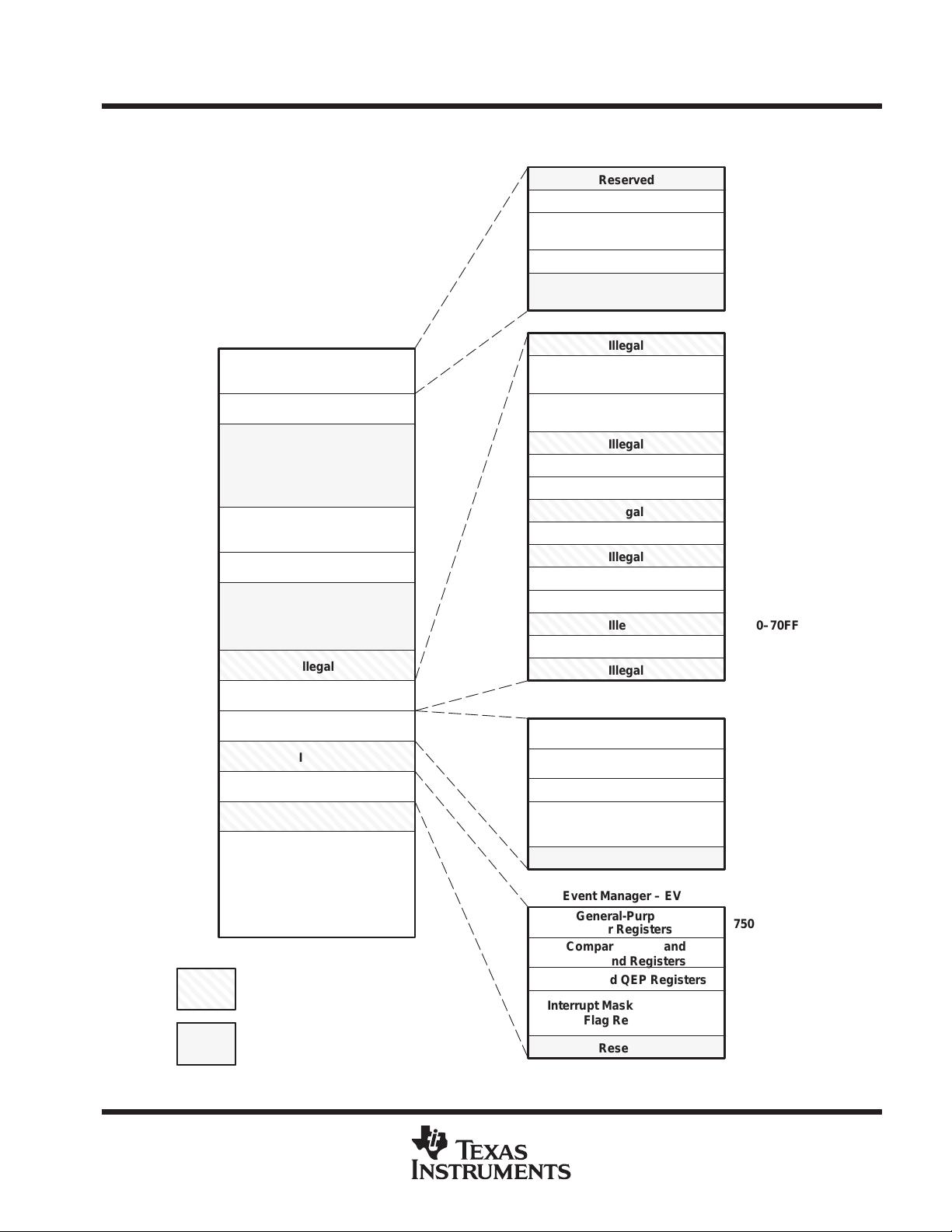
TMS320LC2406, TMS320LC2404, TMS320LC2402
ADVANCE
INFORMATION
peripheral memory map of the ’LF240x/’LC240x
TMS320LF2407, TMS320LF2406, TMS320LF2402
DSP CONTROLLERS
SPRS094C – APRIL 1999 – REVISED OCTOBER 1999
Hex
Reserved
Interrupt-Mask Register
Global-Memory Allocation
Register (Reserved)
Interrupt Flag Register
Emulation Registers
and Reserved
0000
0003
0004
0005
0006
0007
005F
Hex
0000
005F
0060
007F
0080
01FF
0200
02FF
0300
03FF
0400
07FF
0800
6FFF
7000
73FF
7400
743F
7440
74FF
7500
753F
7540
7FFF
8000
FFFF
Illegal
Reserved
Memory-Mapped Registers
and Reserved
On-Chip DARAM B2
Reserved
On-Chip DARAM B0
On-Chip DARAM B1
Reserved
Illegal
Peripheral Frame 1 (PF1)
Peripheral Frame 2 (PF2)
Illegal
Peripheral Frame 3 (PF3)
Illegal
External
“Illegal” indicates that access to
these addresses causes a
nonmaskable interrupt (NMI).
“Reserved” indicates addresses that
are reserved for test and future expansion.
Illegal
System Configuration and
Control Registers
Watchdog Timer Registers
Illegal
SPI
SCI
Illegal
External-Interrupt Registers
Illegal
Digital I/O Control Registers
ADC Control Registers
Illegal
CAN Control Registers
Illegal
Event Manager – EVA
General-Purpose
Timer Registers
Compare, PWM, and
Deadband Registers
Capture and QEP Registers
Interrupt Mask, Vector and
Flag Registers
Reserved
Event Manager – EVB
General-Purpose
Timer Registers
Compare, PWM, and
Deadband Registers
Capture and QEP Registers
Interrupt Mask, Vector, and
Flag Registers
Reserved
7000–700F
7010–701F
7020–702F
7030–703F
7040–704F
7050–705F
7060–706F
7070–707F
7080–708F
7090–709F
70A0–70BF
70C0–70FF
7100–722F
7230–73FF
7400–7408
7411–7419
7420–7429
742C–7431
7432–743F
7500–7508
7511–7519
7520–7529
752C–7531
7532–753F
POST OFFICE BOX 1443 • HOUSTON, TEXAS 77251–1443
21
Page 22

TMS320LF2407, TMS320LF2406, TMS320LF2402
ADVANCE
INFORMATION
TMS320LC2406, TMS320LC2404, TMS320LC2402
DSP CONTROLLERS
SPRS094C – APRIL 1999 – REVISED OCTOBER 1999
device reset and interrupts
The TMS320x240x software-programmable interrupt structure supports flexible on-chip and external interrupt
configurations to meet real-time interrupt-driven application requirements. The ’LF240x recognizes three types
of interrupt sources.
D Reset (hardware- or software-initiated) is unarbitrated by the CPU and takes immediate priority over any
other executing functions. All maskable interrupts are disabled until the reset service routine enables them.
The ’LF240x devices have two sources of reset: an external reset pin and a watchdog timer timeout (reset).
D Hardware-generated interrupts are requested by external pins or by on-chip peripherals. There are two
types:
–
External interrupts
XINT2, PDPINT A, and PDPINTB. These four can be masked both by dedicated enable bits and by t he
CPU’s interrupt mask register (IMR), which can mask each maskable interrupt line at the DSP core.
–
Peripheral interrupts
event manager B, SPI, SCI, WD, CAN, and ADC. They can be masked both by enable bits for each
event in each peripheral and by the CPU’s IMR, which can mask each maskable interrupt line at the DSP
core.
are generated by one of four external pins corresponding to the interrupts XINT1,
are initiated internally by these on-chip peripheral modules: event manager A,
D Software-generated interrupts for the ’LF240x devices include:
–
The INTR instruction.
operand indicates the interrupt vector location to which the CPU branches. This instruction globally
disables maskable interrupts (sets the INTM bit to 1).
–
The NMI instruction.
globally disables maskable interrupts. ’240x devices do not have the NMI hardware signal, only
software activation is provided.
–
The TRAP instruction.
TRAP instruction does
branches to the interrupt service routine, that routine can be interrupted by the maskable hardware
interrupts.
–
An emulator trap.
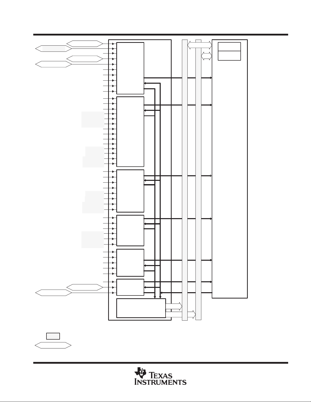
Six core interrupts (INT1–INT6) are expanded using a peripheral interrupt expansion (PIE) module identical to
the ’F24x devices. The PIE manages all the peripheral interrupts from the ’240x peripherals and are grouped to
share the six-core level interrupts. Figure 7 shows the PIE block diagram for hardware-generated interrupts.
The PIE diagram (Figure 7) and the interrupt table (Table 3) explain the grouping and interrupt vector maps.
’LF240x devices have interrupts identical to the ’F24x devices and should be completely code-compatible.
’240x devices also have peripheral interrupts identical to the ’F24x – plus additional interrupts for new
peripherals such as event manager B. Though the new interrupts share the ’24x interrupt grouping, they all have
a unique vector to differentiate among the interrupts. See Table 3 for details.
This instruction allows initialization of any ’LF240x interrupt with software. Its
This instruction forces a branch to interrupt vector location 24h. This instruction
This instruction forces the CPU to branch to interrupt vector location 22h. The
not
disable maskable interrupts (INTM is not set to 1); therefore, when the CPU
This interrupt can be generated with either an INTR instruction or a TRAP instruction.
22
POST OFFICE BOX 1443 • HOUSTON, TEXAS 77251–1443
Page 23
TMS320LF2407, TMS320LF2406, TMS320LF2402
ADVANCE
INFORMATION
TMS320LC2406, TMS320LC2404, TMS320LC2402
DSP CONTROLLERS
SPRS094C – APRIL 1999 – REVISED OCTOBER 1999
PDPINTB
XINT2
XINT2
PDPINTA
ADCINT
XINT1
SPIINT
RXINT
TXINT
CANMBINT
CANERINT
CMP1INT
CMP2INT
CMP3INT
CMP4INT
CMP5INT
CMP6INT
T1PINT
T1CINT
T1UFINT
T1OFINT
T3PINT
T3CINT
T3UFINT
T3OFINT
T2PINT
T2CINT
T2UFINT
T2OFINT
T4PINT
T4CINT
T4UFINT
T4OFINT
CAP1INT
CAP2INT
CAP3INT
CAP4INT
CAP5INT
CAP6INT
SPIINT
RXINT
TXINT
CANMBINT
CANERINT
ADCINT
XINT1
Level 1
IRQ GEN
Level 2
IRQ GEN
Level 3
IRQ GEN
Level 4
IRQ GEN
Level 5
IRQ GEN
Level 6
IRQ GEN
PIVR & Logic
PIRQR#
PIACK#
PIE
IMR
IFR
INT1
INT2
CPU
INT3
INT4
INT5
INT6
IACK
Addr
Data
Bus
Bus
Indicates change with respect to the TMS320F243/F241/C242 data sheets.
Interrupts from external interrupt pins. The remaining interrupts are internal to the peripherals.
Figure 7. Peripheral Interrupt Expansion (PIE) Module Block Diagram for Hardware-Generated Interrupts
POST OFFICE BOX 1443 • HOUSTON, TEXAS 77251–1443
23
Page 24
TMS320LF2407, TMS320LF2406, TMS320LF2402
Power device rotection
0002h
0004h
ADVANCE
INFORMATION
TMS320LC2406, TMS320LC2404, TMS320LC2402
DSP CONTROLLERS
SPRS094C – APRIL 1999 – REVISED OCTOBER 1999
interrupt request structure
Table 3. ’LF240x/’LC240x Interrupt Source Priority and Vectors
INTERRUPT
Reset 1
Reserved 2
NMI 3
PDPINTA 4 0.0 0020h Y EVA
PDPINTB 5 2.0 0019h Y EVB
ADCINT 6
XINT1 7 0.2 0001h Y
XINT2 8
SPIINT 9
RXINT 10
TXINT 11 0.6 0007h Y SCI
CANMBINT 12 0.7 0040 Y CAN
CANERINT 13 0.8 0041 Y CAN
CMP1INT 14 0.9 0021h Y EVA Compare 1 interrupt
CMP2INT 15 0.10 0022h Y EVA Compare 2 interrupt
CMP3INT 16 0.11 0023h Y EVA Compare 3 interrupt
T1PINT 17
T1CINT 18
T1UFINT 19
T1OFINT 20 0.15 002Ah Y EVA Timer 1 overflow interrupt
CMP4INT 21 2.1 0024h Y EVB Compare 4 interrupt
CMP5INT 22 2.2 0025h Y EVB Compare 4 interrupt
CMP6INT 23 2.3 0026h Y EVB Compare 4 interrupt
T3PINT 24 2.4 002Fh Y EVB Timer 3 period interrupt
T3CINT 25 2.5 0030h Y EVB Timer 3 compare interrupt
T3UFINT 26 2.6 0031h Y EVB Timer 3 underflow interrupt
T3OFINT 27 2.7 0032h Y EVB Timer 3 overflow interrupt
†
Refer to the
TMS320F243/’F241/’C242 DSP Controllers System and Peripherals User’s Guide
NAME
CPU
OVERALL
PRIORITY
TMS320C240 DSP Controllers CPU, System, and Instruction Set Reference Guide
INTERRUPT
AND
VECTOR
ADDRESS
RSN
0000h
–
0026h
NMI
0024h
INT1
INT2
BIT
POSITION IN
PIRQRx AND
PIACKRx
0.1 0004h Y ADC
0.3 0011h Y
0.4 0005h Y SPI SPI interrupt pins in high priority
0.5 0006h Y SCI
0.12 0027h Y EVA Timer 1 period interrupt
0.13 0028h Y EVA Timer 1 compare interrupt
0.14 0029h Y EVA Timer 1 underflow interrupt
PERIPHERAL
INTERRUPT
VECTOR
(PIV)
N/A N
N/A N CPU Emulator trap
N/A N
MASKABLE?
(literature number SPRU276) for more information.
SOURCE
PERIPHERAL
MODULE
RS pin,
Watchdog
Nonmaskable
Interrupt
External
Interrupt Logic
External
Interrupt Logic
DESCRIPTION
Reset from pin, watchdog
timeout
Nonmaskable interrupt,
software interrupt only
Power device protection
interrupt pins
ADC interrupt in
high-priority mode
External interrupt pins in high
priority
External interrupt pins in high
priority
SCI receiver interrupt in
high-priority mode
SCI transmitter interrupt in
high-priority mode
CAN mailbox in high-priority
mode
CAN error interrupt in
high-priority mode
(literature number SPRU160) and the
24
New peripheral interrupts and vectors with respect to the ’F243/’F241 devices.
POST OFFICE BOX 1443 • HOUSTON, TEXAS 77251–1443
Page 25
interrupt request structure (continued)
INT3
INT4
000Ah
000Ch
†
ADVANCE
INFORMATION
Table 3.’LF240x/’LC240x Interrupt Source Priority and Vectors (Continued)
TMS320LF2407, TMS320LF2406, TMS320LF2402
TMS320LC2406, TMS320LC2404, TMS320LC2402
DSP CONTROLLERS
SPRS094C – APRIL 1999 – REVISED OCTOBER 1999
CPU
INTERRUPT
NAME
T2PINT 28 1.0 002Bh Y EVA Timer 2 period interrupt
T2CINT 29 1.1 002Ch Y EVA Timer 2 compare interrupt
T2UFINT 30 1.2 002Dh Y EVA Timer 2 underflow interrupt
T2OFINT 31
T4PINT 32
T4CINT 33 2.9 003Ah Y EVB Timer 4 compare interrupt
T4UFINT 34 2.10 003Bh Y EVB Timer 4 underflow interrupt
T4OFINT 35 2.11 003Ch Y EVB Timer 4 overflow interrupt
CAP1INT 36 1.4 0033h Y EVA Capture 1 interrupt
CAP2INT 37 1.5 0034h Y EVA Capture 2 interrupt
CAP3INT 38
CAP4INT 39
CAP5INT 40 2.13 0037h Y EVB Capture 5 interrupt
CAP6INT 41 2.14 0038h Y EVB Capture 6 interrupt
SPIINT 42 1.7 0005h Y SPI SPI interrupt (low priority)
RXINT 43 1.8 0006h Y SCI
TXINT 44
CANMBINT 45
CANERINT 46 1.11 0041h Y CAN
ADCINT 47 1.12 0004h Y ADC
XINT1 48
XINT2 49
Reserved 000Eh N/A Y CPU Analysis interrupt
TRAP N/A 0022h N/A N/A CPU TRAP instruction
Phantom
Interrupt
Vector
INT8–INT16 N/A 0010h–0020h N/A N/A CPU
INT20–INT31 N/A 00028h–0603Fh N/A N/A CPU
†
Refer to the
TMS320F243/’F241/’C242 DSP Controllers System and Peripherals User’s Guide
OVERALL
PRIORITY
N/A N/A 0000h N/A CPU Phantom interrupt vector
TMS320C240 DSP Controllers CPU, System, and Instruction Set Reference Guide
INTERRUPT
AND
VECTOR
ADDRESS
INT3
0006h
INT4
0008h
INT5
INT6
000Ch
BIT
POSITION IN
PIRQRx AND
PIACKRx
1.3 002Eh Y EVA Timer 2 overflow interrupt
2.8 0039h Y EVB Timer 4 period interrupt
1.6 0035h Y EVA Capture 3 interrupt
2.12 0036h Y EVB Capture 4 interrupt
1.9 0007h Y SCI
1.10 0040h Y CAN
1.13 0001h Y
1.14 0011h Y
PERIPHERAL
INTERRUPT
VECTOR
(PIV)
MASK-
ABLE?
(literature number SPRU276) for more information.
SOURCE
PERIPHERAL
MODULE
External
Interrupt Logic
External
Interrupt Logic
(literature number SPRU160) and the
DESCRIPTION
SCI receiver interrupt
(low-priority mode)
SCI transmitter interrupt
(low-priority mode)
CAN mailbox interrupt
(low-priority mode)
CAN error interrupt
(low-priority mode)
ADC interrupt
(low priority)
External interrupt pins
(low-priority mode)
External interrupt pins
(low-priority mode)
Software interrupt vectors
New peripheral interrupts and vectors with respect to the ’F243/’F241 devices.
POST OFFICE BOX 1443 • HOUSTON, TEXAS 77251–1443
25
Page 26

TMS320LF2407, TMS320LF2406, TMS320LF2402
ADVANCE
INFORMATION
TMS320LC2406, TMS320LC2404, TMS320LC2402
DSP CONTROLLERS
SPRS094C – APRIL 1999 – REVISED OCTOBER 1999
DSP CPU Core
The TMS320x240x devices use an advanced Harvard-type architecture that maximizes processing power by
maintaining two separate memory bus structures — program and data — for full-speed execution. This multiple
bus structure allows data and instructions to be read simultaneously. Instructions support data transfers
between program memory and data memory . This architecture permits coefficients that are stored in program
memory to be read in RAM, thereby eliminating the need for a separate coefficient ROM. This, coupled with a
four-deep pipeline, allows the ’LF240x/’LC240x devices to execute most instructions in a single cycle. See the
architectural block diagram of the ’24x DSP Core for more information.
TMS320x240x instruction set
The ’x240x microprocessor implements a comprehensive instruction set that supports both numeric-intensive
signal-processing operations and general-purpose applications, such as multiprocessing and high-speed
control. Source code for the ’C1x and ’C2x DSPs is upwardly compatible with the ’x243/’x241 and ’240x devices.
For maximum throughput, the next instruction is prefetched while the current one is being executed. Because
the same data lines are used to communicate to external data, program, or I/O space, the number of cycles an
instruction requires to execute varies, depending upon whether the next data operand fetch is from internal or
external memory . Highest throughput is achieved by maintaining data memory on chip and using either internal
or fast external program memory.
addressing modes
scan-based emulation
The TMS320x240x instruction set provides four basic memory-addressing modes: direct, indirect, immediate,
and register.
In direct addressing, the instruction word contains the lower seven bits of the data memory address. This field
is concatenated with the nine bits of the data memory page pointer (DP) to form the 16-bit data memory address.
Therefore, in the direct-addressing mode, data memory is paged effectively with a total of 512 pages, with each
page containing 128 words.
Indirect addressing accesses data memory through the auxiliary registers. In this addressing mode, the address
of the instruction operand is contained in the currently selected auxiliary register. Eight auxiliary registers
(AR0–AR7) provide flexible and powerful indirect addressing. T o select a specific auxiliary register , the auxiliary
register pointer (ARP) is loaded with a value from 0 to 7 for AR0 through AR7, respectively.
TMS320x2xx devices incorporate scan-based emulation logic for code-development and hardwaredevelopment support. Scan-based emulation allows the emulator to control the processor in the system without
the use of intrusive cables to the full pinout of the device. The scan-based emulator communicates with the ’x2xx
by way of the IEEE 1149.1-compatible (JTAG) interface. The ’x240x DSPs, like the TMS320F243/241,
TMS320F206, TMS320C203, and TMS320LC203, do not include boundary scan. The scan chain of these
devices is useful for emulation function only.
26
POST OFFICE BOX 1443 • HOUSTON, TEXAS 77251–1443
Page 27
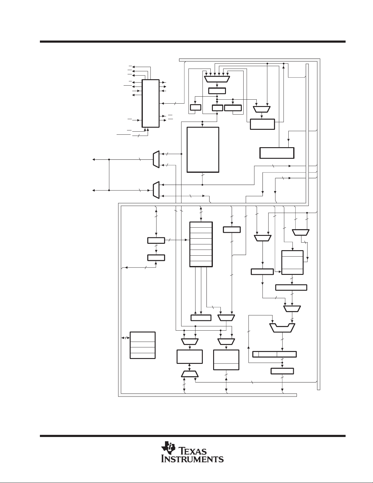
TMS320LF2407, TMS320LF2406, TMS320LF2402
ADVANCE
INFORMATION
TMS320LC2406, TMS320LC2404, TMS320LC2402
DSP CONTROLLERS
SPRS094C – APRIL 1999 – REVISED OCTOBER 1999
functional block diagram of the ’240x DSP CPU
IS
DS
PS
Control
MUXMUX
ARP(3)
ARB(3)
XTAL1
CLKOUT
XTAL2
RD
WE
16
16
3
3
3
A15–A0
D15–D0
R/W
STRB
READY
MP/MC
XINT[1–2]
16
XF
RS
Data Bus
Memory Map
GREG (16)
2
16
16
3
Register
IMR (16)
IFR (16)
16
1616
MUX
Data/Prog
DARAM
B0 (256 × 16)
MUX
PC
FLASH EEPROM/
ROM
16
16
AR0(16)
AR1(16)
AR2(16)
AR3(16)
AR4(16)
AR5(16)
AR6(16)
AR7(16)
ARAU(16)
16
MUX
NPAR
PAR MST ACK
16
16
DP(9)
MUX
MUX
Data
DARAM
B2 (32 × 16)
B1 (256 × 16)
16
Program Bus
9
9
16
MUX
Stack 8 × 16
16
7
LSB
from
IR
MUX
ISCALE (0–16)
32
16
Program Control
(PCTRL)
16
16
16
16
PSCALE (–6,ā0,ā1,ā4)
CALU(32)
ACCL(16)ACCH(16)C
OSCALE (0–7)
Data Bus
TREG0(16)
Multiplier
PREG(32)
32
MUX
32
32
16
3232
32
MUX
Data Bus
1616
16
Program Bus
Program Bus
NOTES: A. See T able 4 for symbol descriptions.
B. For clarity, the data and program buses are shown as single buses although they include address and data bits.
C. Refer to the TMS320F243, TMS320F241 DSP Controllers data sheet (literature number SPRS064), the TMS320C240,
TMS320F240 DSP Controllers data sheet (literature number SPRS042), and the
Instruction Set Reference Guide
(literature number SPRU160) for CPU instruction set information.
POST OFFICE BOX 1443 • HOUSTON, TEXAS 77251–1443
TMS320C240 DSP Controllers CPU, System, and
27
Page 28
TMS320LF2407, TMS320LF2406, TMS320LF2402
ADVANCE
INFORMATION
TMS320LC2406, TMS320LC2404, TMS320LC2402
DSP CONTROLLERS
SPRS094C – APRIL 1999 – REVISED OCTOBER 1999
’240x legend for the internal hardware
SYMBOL NAME DESCRIPTION
ACC Accumulator
ARAU
AUX
REGS
C Carry
CALU
DARAM Dual-Access RAM
DP
GREG
IMR
IFR
INT# Interrupt Traps A total of 32 interrupts by way of hardware and/or software are available.
ISCALE
MPY Multiplier
MSTACK Micro Stack
MUX Multiplexer Multiplexes buses to a common input
NPAR
OSCALE
PAR
PC Program Counter
PCTRL
Auxiliary Register
Arithmetic Unit
Auxiliary Registers
0–7
Central Arithmetic
Logic Unit
Data Memory
Page Pointer
Global Memory
Allocation
Register
Interrupt Mask
Register
Interrupt Flag
Register
Input Data-Scaling
Shifter
Next Program
Address Register
Output
Data-Scaling
Shifter
Program Address
Register
Program
Controller
Table 4. Legend for the ’240x DSP CPU Internal Hardware
32-bit register that stores the results and provides input for subsequent CALU operations. Also includes shift
and rotate capabilities
An unsigned, 16-bit arithmetic unit used to calculate indirect addresses using the auxiliary registers as inputs
and outputs
These 16-bit registers are used as pointers to anywhere within the data space address range. They are
operated upon by the ARAU and are selected by the auxiliary register pointer (ARP). AR0 can also be used
as an index value for AR updates of more than one and as a compare value to AR.
Register carry output from CALU. C is fed back into the CALU for extended arithmetic operation. The C bit
resides in status register 1 (ST1), and can be tested in conditional instructions. C is also used in accumulator
shifts and rotates.
32-bit-wide main arithmetic logic unit for the TMS320C2xx core. The CALU executes 32-bit operations in a
single machine cycle. CALU operates on data coming from ISCALE or PSCALE with data from ACC, and
provides status results to PCTRL.
If the on-chip RAM configuration control bit (CNF) is set to 0, the reconfigurable data dual-access RAM
(DARAM) block B0 is mapped to data space; otherwise, B0 is mapped to program space. Blocks B1 and B2
are mapped to data memory space only, at addresses 0300–03FF and 0060–007F, respectively. Blocks 0
and 1 contain 256 words, while block 2 contains 32 words.
The 9-bit DP register is concatenated with the seven least significant bits (LSBs) of an instruction word to
form a direct memory address of 16 bits. DP can be modified by the LST and LDP instructions.
GREG specifies the size of the global data memory space. Since the global memory space is not used in
the ’240x devices, this register is reserved.
IMR individually masks or enables the seven interrupts.
The 7-bit IFR indicates that the TMS320C2xx has latched an interrupt from one of the seven maskable
interrupts.
16- to 32-bit barrel left-shifter. ISCALE shifts incoming 16-bit data 0 to16 positions left, relative to the 32-bit
output within the fetch cycle; therefore, no cycle overhead is required for input scaling operations.
16 × 16-bit multiplier to a 32-bit product. MPY executes multiplication in a single cycle. MPY operates either
signed or unsigned 2s-complement arithmetic multiply.
MSTACK provides temporary storage for the address of the next instruction to be fetched when program
address-generation logic is used to generate sequential addresses in data space.
NPAR holds the program address to be driven out on the PAB in the next cycle.
16- to 32-bit barrel left-shifter. OSCALE shifts the 32-bit accumulator output 0 to 7 bits left for quantization
management and outputs either the 16-bit high- or low-half of the shifted 32-bit data to the data-write data
bus (DWEB).
PAR holds the address currently being driven on P AB for as many cycles as it takes to complete all memory
operations scheduled for the current bus cycle.
PC increments the value from NPAR to provide sequential addresses for instruction-fetching and sequential
data-transfer operations.
PCTRL decodes instruction, manages the pipeline, stores status, and decodes conditional operations.
28
POST OFFICE BOX 1443 • HOUSTON, TEXAS 77251–1443
Page 29
TMS320LF2407, TMS320LF2406, TMS320LF2402
ADVANCE
INFORMATION
TMS320LC2406, TMS320LC2404, TMS320LC2402
DSP CONTROLLERS
SPRS094C – APRIL 1999 – REVISED OCTOBER 1999
’240x legend for the internal hardware (continued)
Table 4. Legend for the ’240x DSP CPU Internal Hardware (Continued)
SYMBOL NAME DESCRIPTION
PREG Product Register 32-bit register holds results of 16 × 16 multiply
0-, 1-, or 4-bit left shift, or 6-bit right shift of multiplier product. The left-shift options are used to manage the
PSCALE
STACK Stack
TREG
Product-Scaling
Shifter
Temporary
Register
status and control registers
Two status registers, ST0 and ST1, contain the status of various conditions and modes. These registers can
be stored into data memory and loaded from data memory , thus allowing the status of the machine to be saved
and restored for subroutines.
The load status register (LST) instruction is used to write to ST0 and ST1. The store status register (SST)
instruction is used to read from ST0 and ST1 — except for the INTM bit, which is not affected by the LST
instruction. The individual bits of these registers can be set or cleared when using the SETC and CLRC
instructions. Figure 8 shows the organization of status registers ST0 and ST1, indicating all status bits contained
in each. Several bits in the status registers are reserved and are read as logic 1s. Table 5 lists status register
field definitions.
additional sign bits resulting from the 2s-complement multiply. The right-shift option is used to scale down
the number to manage overflow of product accumulation in the CALU. PSCALE resides in the path from the
32-bit product shifter and from either the CALU or the data-write data bus (DWEB), and requires no cycle
overhead.
STACK is a block of memory used for storing return addresses for subroutines and interrupt-service
routines, or for storing data. The ’C2xx stack is 16-bit wide and eight-level deep.
16-bit register holds one of the operands for the multiply operations. TREG holds the dynamic shift count
for the LACT, ADDT, and SUBT instructions. TREG holds the dynamic bit position for the BITT instruction.
15 13 12 11 10 9 8 0
ST0
15 13 12 11 10 9 8 7 6 5 4 3 2 1 0
ST1
ARP OV OVM 1 INTM DP
ARB CNF TC SXM C 1 1 1 1 XF 1 1 PM
Figure 8. Organization of Status Registers ST0 and ST1
Table 5. Status Register Field Definitions
FIELD FUNCTION
ARB
ARP
C
CNF
Auxiliary register pointer buffer . When the ARP is loaded into ST0, the old ARP value is copied to the ARB except during an LST
instruction. When the ARB is loaded by way of an LST #1 instruction, the same value is also copied to the ARP.
Auxiliary register (AR) pointer. ARP selects the AR to be used in indirect addressing. When the ARP is loaded, the old ARP value
is copied to the ARB register. ARP can be modified by memory-reference instructions when using indirect addressing, and by the
LARP, MAR, and LST instructions. The ARP is also loaded with the same value as ARB when an LST #1 instruction is executed.
Carry bit. C is set to 1 if the result of an addition generates a carry, or reset to 0 if the result of a subtraction generates a borrow.
Otherwise, C is reset after an addition or set after a subtraction, except if the instruction is ADD or SUB with a 16-bit shift. In these
cases, ADD can only set and SUB can only reset the carry bit, but cannot affect it otherwise. The single-bit shift and rotate
instructions also affect C, as well as the SETC, CLRC, and LST #1 instructions. Branch instructions have been provided to branch
on the status of C. C is set to 1 on a reset.
On-chip RAM configuration control bit. If CNF is set to 0, the reconfigurable data dual-access RAM blocks are mapped to data
space; otherwise, they are mapped to program space. The CNF can be modified by the SETC CNF, CLRC CNF, and LST #1
instructions. RS
sets the CNF to 0.
POST OFFICE BOX 1443 • HOUSTON, TEXAS 77251–1443
29
Page 30
TMS320LF2407, TMS320LF2406, TMS320LF2402
ADVANCE
INFORMATION
TMS320LC2406, TMS320LC2404, TMS320LC2402
DSP CONTROLLERS
SPRS094C – APRIL 1999 – REVISED OCTOBER 1999
status and control registers (continued)
Table 5. Status Register Field Definitions (Continued)
FIELD FUNCTION
DP
INTM
OV
OVM
PM
SXM
TC
XF
Data memory page pointer. The 9-bit DP register is concatenated with the seven LSBs of an instruction word to form a direct
memory address of 16 bits. DP can be modified by the LST and LDP instructions.
Interrupt mode bit. When INTM is set to 0, all unmasked interrupts are enabled. When set to 1, all maskable interrupts are disabled.
INTM is set and reset by the SETC INTM and CLRC INTM instructions. RS
and NMI interrupts. Note that INTM is unaffected by the LST instruction. This bit is set to 1 by reset. It is also set to 1 when
RS
a maskable interrupt trap is taken.
Overflow flag bit. As a latched overflow signal, OV is set to 1 when overflow occurs in the arithmetic logic unit (ALU). Once an
overflow occurs, the OV remains set until a reset, BCND/D on OV/NOV, or LST instruction clears OV .
Overflow mode bit. When OVM is set to 0, overflowed results overflow normally in the accumulator. When set to 1, the accumulator
is set to either its most positive or negative value upon encountering an overflow. The SETC and CLRC instructions set and reset
this bit, respectively. LST can also be used to modify the OVM.
Product shift mode. If these two bits are 00, the multiplier’s 32-bit product is loaded into the ALU with no shift. If PM = 01, the PREG
output is left-shifted one place and loaded into the ALU, with the LSB zero-filled. If PM = 10, the PREG output is left-shifted by four
bits and loaded into the ALU, with the LSBs zero-filled. PM = 11 produces a right shift of six bits, sign-extended. Note that the PREG
contents remain unchanged. The shift takes place when transferring the contents of the PREG to the ALU. PM is loaded by the
SPM and LST #1 instructions. PM is cleared by RS
Sign-extension mode bit. SXM = 1 produces sign extension on data as it is passed into the accumulator through the scaling shifter.
SXM = 0 suppresses sign extension. SXM does not affect the definitions of certain instructions; for example, the ADDS instruction
suppresses sign extension regardless of SXM. SXM is set by the SETC SXM instruction and reset by the CLRC SXM instruction
and can be loaded by the LST #1 instruction. SXM is set to 1 by reset.
T est/control flag bit. TC is affected by the BIT, BITT , CMPR, LST #1, and NORM instructions. TC is set to a 1 if a bit tested by BIT
or BITT is a 1, if a compare condition tested by CMPR exists between AR (ARP) and AR0, if the exclusive-OR function of the two
most significant bits (MSBs) of the accumulator is true when tested by a NORM instruction. The conditional branch, call, and return
instructions can execute based on the condition of TC.
XF pin status bit. XF indicates the state of the XF pin, a general-purpose output pin. XF is set by the SETC XF instruction and reset
by the CLRC XF instruction. XF is set to 1 by reset.
also sets INTM. INTM has no effect on the unmaskable
.
central processing unit
input scaling shifter
The TMS320x240x central processing unit (CPU) contains a 16-bit scaling shifter, a 16 x 16-bit parallel
multiplier, a 32-bit central arithmetic logic unit (CALU), a 32-bit accumulator, and additional shifters at the
outputs of both the accumulator and the multiplier. This section describes the CPU components and their
functions. The functional block diagram shows the components of the CPU.
The TMS320x240x provides a scaling shifter with a 16-bit input connected to the data bus and a 32-bit output
connected to the CALU. This shifter operates as part of the path of data coming from program or data space
to the CALU and requires no cycle overhead. It is used to align the 16-bit data coming from memory to the 32-bit
CALU. This is necessary for scaling arithmetic as well as aligning masks for logical operations.
The scaling shifter produces a left shift of 0 to 16 on the input data. The LSBs of the output are filled with zeros;
the MSBs can either be filled with zeros or sign-extended, depending upon the value of the SXM bit
(sign-extension mode) of status register ST1. The shift count is specified by a constant embedded in the
instruction word or by a value in TREG. The shift count in the instruction allows for specific scaling or alignment
operations specific to that point in the code. The TREG base shift allows the scaling factor to be adaptable to
the system’s performance.
30
POST OFFICE BOX 1443 • HOUSTON, TEXAS 77251–1443
Page 31

TMS320LF2407, TMS320LF2406, TMS320LF2402
ADVANCE
INFORMATION
TMS320LC2406, TMS320LC2404, TMS320LC2402
DSP CONTROLLERS
SPRS094C – APRIL 1999 – REVISED OCTOBER 1999
multiplier
The TMS320x240x devices use a 16 x 16-bit hardware multiplier that is capable of computing a signed or an
unsigned 32-bit product in a single machine cycle. All multiply instructions, except the MPYU (multiply unsigned)
instruction, perform a signed multiply operation. That is, two numbers being multiplied are treated as
2s-complement numbers, and the result is a 32-bit 2s-complement number. There are two registers associated
with the multiplier, as follow:
D 16-bit temporary register (TREG) that holds one of the operands for the multiplier
D 32-bit product register (PREG) that holds the product
Four product-shift modes (PM) are available at the PREG output (PSCALE). These shift modes are useful for
performing multiply/accumulate operations, performing fractional arithmetic, or justifying fractional products.
The PM field of status register ST1 specifies the PM shift mode, as shown in Table 6.
Table 6. PSCALE Product-Shift Modes
PM SHIFT DESCRIPTION
00 No shift Product feed to CALU or data bus with no shift
01 Left 1 Removes the extra sign bit generated in a 2s-complement multiply to produce a Q31 product
10 Left 4
11 Right 6 Scales the product to allow up to 128 product accumulation without the possibility of accumulator overflow
Removes the extra 4 sign bits generated in a 16x13 2s-complement multiply to a produce a Q31 product when
using the multiply-by-a-13-bit constant
The product can be shifted one bit to compensate for the extra sign bit gained in multiplying two 16-bit
2s-complement numbers (MPY instruction). A four-bit shift is used in conjunction with the MPY instruction with
a short immediate value (13 bits or less) to eliminate the four extra sign bits gained in multiplying a 16-bit number
by a 13-bit number. Finally, the output of PREG can be right-shifted 6 bits to enable the execution of up to
128 consecutive multiply/accumulates without the possibility of overflow.
The L T (load TREG) instruction normally loads TREG to provide one operand (from the data bus), and the MPY
(multiply) instruction provides the second operand (also from the data bus). A multiplication also can be
performed with a 13-bit immediate operand when using the MPY instruction. Then, a product is obtained every
two cycles. When the code is executing multiple multiplies and product sums, the CPU supports the pipelining
of the TREG load operations with CALU operations using the previous product. The pipeline operations that
run in parallel with loading the TREG include: load ACC with PREG (L TP); add PREG to ACC (L TA); add PREG
to ACC and shift TREG input data (DMOV) to next address in data memory (L TD); and subtract PREG from ACC
(L TS).
Two multiply/accumulate instructions (MAC and MACD) fully utilize the computational bandwidth of the
multiplier, allowing both operands to be processed simultaneously. The data for these operations can be
transferred to the multiplier each cycle by way of the program and data buses. This facilitates single-cycle
multiply/accumulates when used with the repeat (RPT) instruction. In these instructions, the coefficient
addresses are generated by program address generation (PAGEN) logic, while the data addresses are
generated by data address generation (DAGEN) logic. This allows the repeated instruction to access the values
from the coefficient table sequentially and step through the data in any of the indirect addressing modes.
The MACD instruction, when repeated, supports filter constructs (weighted running averages) so that as the
sum-of-products is executed, the sample data is shifted in memory to make room for the next sample and to
throw away the oldest sample.
POST OFFICE BOX 1443 • HOUSTON, TEXAS 77251–1443
31
Page 32

TMS320LF2407, TMS320LF2406, TMS320LF2402
ADVANCE
INFORMATION
TMS320LC2406, TMS320LC2404, TMS320LC2402
DSP CONTROLLERS
SPRS094C – APRIL 1999 – REVISED OCTOBER 1999
multiplier (continued)
The MPYU instruction performs an unsigned multiplication, which greatly facilitates extended-precision
arithmetic operations. The unsigned contents of TREG are multiplied by the unsigned contents of the addressed
data memory location, with the result placed in PREG. This process allows the operands of greater than 16 bits
to be broken down into 16-bit words and processed separately to generate products of greater than 32 bits. The
SQRA (square/add) and SQRS (square/subtract) instructions pass the same value to both inputs of the
multiplier for squaring a data memory value.
After the multiplication of two 16-bit numbers, the 32-bit product is loaded into the 32-bit product register
(PREG). The product from PREG can be transferred to the CALU or to data memory by way of the SPH (store
product high) and SPL (store product low) instructions. Note: the transfer of PREG to either the CALU or data
bus passes through the PSCALE shifter, and therefore is af fected by the product shift mode defined by PM. This
is important when saving PREG in an interrupt-service-routine context save as the PSCALE shift effects cannot
be modeled in the restore operation. PREG can be cleared by executing the MPY #0 instruction. The product
register can be restored by loading the saved low half into TREG and executing a MPY #1 instruction. The high
half, then, is loaded using the LPH instruction.
central arithmetic logic unit
The TMS320x240x central arithmetic logic unit (CALU) implements a wide range of arithmetic and logical
functions, the majority of which execute in a single clock cycle. This ALU is referred to as central to differentiate
it from a second ALU used for indirect-address generation called the auxiliary register arithmetic unit (ARAU).
Once an operation is performed in the CALU, the result is transferred to the accumulator (ACC) where additional
operations, such as shifting, can occur. Data that is input to the CALU can be scaled by ISCALE when coming
from one of the data buses (DRDB or PRDB) or scaled by PSCALE when coming from the multiplier.
The CALU is a general-purpose ALU that operates on 16-bit words taken from data memory or derived from
immediate instructions. In addition to the usual arithmetic instructions, the CALU can perform Boolean
operations, facilitating the bit-manipulation ability required for a high-speed controller. One input to the CALU
is always provided from the accumulator, and the other input can be provided from the product register (PREG)
of the multiplier or the output of the scaling shifter (that has been read from data memory or from the ACC). After
the CALU has performed the arithmetic or logical operation, the result is stored in the accumulator.
The TMS320x240x devices support floating-point operations for applications requiring a large dynamic range.
The NORM (normalization) instruction is used to normalize fixed-point numbers contained in the accumulator
by performing left shifts. The four bits of the TREG define a variable shift through the scaling shifter for the
LACT/ADDT/SUBT (load/add to /subtract from accumulator with shift specified by TREG) instructions. These
instructions are useful in floating-point arithmetic where a number needs to be denormalized — that is,
floating-point to fixed-point conversion. They are also useful in the execution of an automatic gain control (AGC)
going into a filter. The BITT (bit test) instruction provides testing of a single bit of a word in data memory based
on the value contained in the four LSBs of TREG.
The CALU overflow saturation mode can be enabled/disabled by setting/resetting the OVM bit of ST0. When
the CALU is in the overflow saturation mode and an overflow occurs, the overflow flag is set and the accumulator
is loaded with either the most positive or the most negative value representable in the accumulator, depending
on the direction of the overflow. The value of the accumulator at saturation is 07FFFFFFFh (positive) or
080000000h (negative). If the OVM (overflow mode) status register bit is reset and an overflow occurs, the
overflowed results are loaded into the accumulator with modification. (Note that logical operations cannot result
in overflow.)
The CALU can execute a variety of branch instructions that depend on the status of the CALU and the
accumulator. These instructions can be executed conditionally based on any meaningful combination of these
status bits. For overflow management, these conditions include OV (branch on overflow) and EQ (branch on
accumulator equal to zero). In addition, the BACC (branch to address in accumulator) instruction provides the
ability to branch to an address specified by the accumulator (computed goto). Bit test instructions (BIT and
BITT), which do not affect the accumulator, allow the testing of a specified bit of a word in data memory.
32
POST OFFICE BOX 1443 • HOUSTON, TEXAS 77251–1443
Page 33

TMS320LF2407, TMS320LF2406, TMS320LF2402
ADVANCE
INFORMATION
TMS320LC2406, TMS320LC2404, TMS320LC2402
DSP CONTROLLERS
SPRS094C – APRIL 1999 – REVISED OCTOBER 1999
central arithmetic logic unit (continued)
The CALU also has an associated carry bit that is set or reset depending on various operations within the device.
The carry bit allows more efficient computation of extended-precision products and additions or subtractions.
It is also useful in overflow management. The carry bit is affected by most arithmetic instructions as well as the
single-bit shift and rotate instructions. It is not affected by loading the accumulator , logical operations, or other
such non-arithmetic or control instructions.
The ADDC (add to accumulator with carry) and SUBB (subtract from accumulator with borrow) instructions use
the previous value of carry in their addition/subtraction operation.
The one exception to the operation of the carry bit is in the use of ADD with a shift count of 16 (add to high
accumulator) and SUB with a shift count of 16 (subtract from high accumulator) instructions. This case of the
ADD instruction can set the carry bit only if a carry is generated, and this case of the SUB instruction can reset
the carry bit only if a borrow is generated; otherwise, neither instruction affects it.
Two conditional operands, C and NC, are provided for branching, calling, returning, and conditionally executing,
based upon the status of the carry bit. The SETC, CLRC, and LST #1 instructions also can be used to load the
carry bit. The carry bit is set to one on a hardware reset.
accumulator
The 32-bit accumulator is the registered output of the CALU. It can be split into two 16-bit segments for storage
in data memory. Shifters at the output of the accumulator provide a left shift of 0 to 7 places. This shift is
performed while the data is being transferred to the data bus for storage. The contents of the accumulator
remain unchanged. When the postscaling shifter is used on the high word of the accumulator (bits 16–31), the
MSBs are lost and the LSBs are filled with bits shifted in from the low word (bits 0–15). When the postscaling
shifter is used on the low word, the LSBs are zero-filled.
The SFL and SFR (in-place one-bit shift to the left / right) instructions and the ROL and ROR (rotate to the
left/right) instructions implement shifting or rotating of the contents of the accumulator through the carry bit. The
SXM bit affects the definition of the SFR (shift accumulator right) instruction. When SXM = 1, SFR performs an
arithmetic right shift, maintaining the sign of the accumulator data. When SXM = 0, SFR performs a logical shift,
shifting out the LSBs and shifting in a zero for the MSB. The SFL (shift accumulator left) instruction is not affected
by the SXM bit and behaves the same in both cases, shifting out the MSB and shifting in a zero. Repeat (RPT)
instructions can be used with the shift and rotate instructions for multiple-bit shifts.
auxiliary registers and auxiliary-register arithmetic unit (ARAU)
The ’240x provides a register file containing eight auxiliary registers (AR0– AR7). The auxiliary registers are
used for indirect addressing of the data memory or for temporary data storage. Indirect auxiliary-register
addressing allows placement of the data memory address of an instruction operand into one of the auxiliary
registers. These registers are referenced with a 3-bit auxiliary register pointer (ARP) that is loaded with a value
from 0 through 7, designating AR0 through AR7, respectively . The auxiliary registers and the ARP can be loaded
from data memory , the ACC, the product register, or by an immediate operand defined in the instruction. The
contents of these registers also can be stored in data memory or used as inputs to the CALU.
The auxiliary register file (AR0–AR7) is connected to the ARAU. The ARAU can autoindex the current auxiliary
register while the data memory location is being addressed. Indexing either by ±1 or by the contents of the AR0
register can be performed. As a result, accessing tables of information does not require the CALU for address
manipulation; therefore, the CALU is free for other operations in parallel.
POST OFFICE BOX 1443 • HOUSTON, TEXAS 77251–1443
33
Page 34

TMS320LF2407, TMS320LF2406, TMS320LF2402
ADVANCE
INFORMATION
TMS320LC2406, TMS320LC2404, TMS320LC2402
DSP CONTROLLERS
SPRS094C – APRIL 1999 – REVISED OCTOBER 1999
internal memory
The TMS320x240x devices are configured with the following memory modules:
D Dual-access random-access memory (DARAM)
D Single-access random-access memory (SARAM)
D Flash
D ROM
D Boot ROM
dual-access RAM (DARAM)
There are 544 words × 16 bits of DARAM on the ’240x devices. The ’240x DARAM allows writes to and reads
from the RAM in the same cycle. The DARAM is configured in three blocks: block 0 (B0), block 1 (B1), and
block 2 (B2). Block 1 contains 256 words and Block 2 contains 32 words, and both blocks are located only in
data memory space. Block 0 contains 256 words, and can be configured to reside in either data or program
memory space. The SETC CNF (configure B0 as data memory) and CLRC CNF (configure B0 as program
memory) instructions allow dynamic configuration of the memory maps through software.
When using on-chip RAM or high-speed external memory , the ’240x runs at full speed with no wait states. The
ability of the DARAM to allow two accesses to be performed in one cycle, coupled with the parallel nature of
the ’240x architecture, enables the device to perform three concurrent memory accesses in any given machine
cycle. Externally, the READY line or on-chip software wait-state generator can be used to interface the ’240x
to slower, less expensive external memory . Downloading programs from slow of f-chip memory to on-chip RAM
can speed processing while cutting system costs.
single-access RAM (SARAM)
flash EEPROM
There are 2K words × 16 bits of SARAM on some of the ’240x devices.
reads from the RAM in the same cycle. The PON and DON bits select SARAM (2K) mapping in program space,
data space, or both. See T able 18 for details on the SCSR2 register and the PON and DON bits. At reset, these
bits are 1 1, and the on-chip SARAM is mapped in both the program and data spaces. The SARAM addresses
(8000h in program memory and 0800h in data memory) are accessible in external memory space, if the on-chip
SARAM is not enabled.
Flash EEPROM provides an attractive alternative to masked program ROM. Like ROM, flash is nonvolatile.
However, it has the advantage of “in-target” reprogrammability. The ’LF240x incorporates one 32K 16-bit
flash EEPROM module in program space. This type of memory expands the capabilities of the ’LF240x in the
areas of prototyping, early field-testing, and single-chip applications. The flash module has multiple sectors that
can be individually protected while erasing or programming. The sector size is non-uniform and partitioned as
4K/12K/12K/4K sectors.
Unlike most discrete flash memory , the ’LF240x flash does not require a dedicated state machine, because the
algorithms for programming and erasing the flash are executed by the DSP core. This enables several
advantages, including: reduced chip size and sophisticated, adaptive algorithms. For production programming,
the IEEE Standard 1149.1
algorithms and flash code. This flash requires 5 V for programming (at V
at zero wait state while the device is powered at 3.3 V.
‡
(JTAG) scan port provides easy access to the on-chip RAM for downloading the
†
The ’240x SARAM allows writes to and
pin only) the array . The flash runs
CCP
†
See Table 1 for device-specific features.
‡
IEEE Standard 1149.1–1990, IEEE Standard Test Access Port.
34
POST OFFICE BOX 1443 • HOUSTON, TEXAS 77251–1443
Page 35

TMS320LF2407, TMS320LF2406, TMS320LF2402
ADV ANCE
INFORMATION
TMS320LC2406, TMS320LC2404, TMS320LC2402
DSP CONTROLLERS
SPRS094C – APRIL 1999 – REVISED OCTOBER 1999
ROM
The ’LC240x devices contain mask-programmable ROM located in program memory space. Customers can
arrange to have this ROM programmed with contents unique to any particular application. See Table 1 for the
ROM memory capacity of each ’LC240x device.
boot ROM
Boot ROM is a 256-word ROM memory mapped in program space 0000–00FF . This ROM will be enabled if the
BOOTEN
pin is low at reset. Boot ROM can also be enabled by writing 1 to the SCSR2.3 bit and disabled by writing 0
to this bit.
The boot ROM has a generic bootloader to transfer code through SCI or SPI ports. The incoming code should
disable the BOOT_ROM bit by writing 0 to bit 3 of the SCSR2 register, or else, the whole flash array will not be
enabled.
pin is low during reset. The BOOT_EN bit (bit 3 of the SCSR2 register) will be set to 1 if the BOOTEN
POST OFFICE BOX 1443 • HOUSTON, TEXAS 77251–1443
35
Page 36

TMS320LF2407, TMS320LF2406, TMS320LF2402
ADVANCE
INFORMATION
TMS320LC2406, TMS320LC2404, TMS320LC2402
DSP CONTROLLERS
SPRS094C – APRIL 1999 – REVISED OCTOBER 1999
PERIPHERALS
The integrated peripherals of the TMS320x240x are described in the following subsections:
D Two event-manager modules (EVA, EVB)
D Enhanced analog-to-digital converter (ADC) module
D Controller area network (CAN) module
D Serial communications interface (SCI) module
D Serial peripheral interface (SPI) module
D PLL-based clock module
D Digital I/O and shared pin functions
D External memory interfaces (’LF2407 only)
D Watchdog (WD) timer module
event manager modules (EVA, EVB)
The event-manager modules include general-purpose (GP) timers, full-compare/PWM units, capture units, and
quadrature-encoder pulse (QEP) circuits. EVA ’s and EVB’s timers, compare units, and capture units function
identically. However, timer/unit names differ for EVA and EVB. Table 7 shows the module and signal names
used. T able 7 shows the features and functionality available for the event-manager modules and highlights EV A
nomenclature.
EVENT MANAGER MODULES EVA MODULE SIGNAL EVB MODULE SIGNAL
GP Timers
Compare Units
Capture Units
QEP
External Inputs
Event managers A and B have identical peripheral register sets with EVA starting at 7400h and EVB starting
at 7500h. The paragraphs in this section describe the function of GP timers, compare units, capture units, and
QEPs using EVA nomenclature. These paragraphs are applicable to EVB with regard to function—however,
module/signal names would differ.
Table 7. Module and Signal Names for EVA and EVB
Timer 1
Timer 2
Compare 1
Compare 2
Compare 3
Capture 1
Capture 2
Capture 3
QEP1
QEP2
Direction
External Clock
T1PWM/T1CMP
T2PWM/T2CMP
PWM1/2
PWM3/4
PWM5/6
CAP1
CAP2
CAP3
QEP1
QEP2
TDIRA
TCLKINA
Timer 3
Timer 4
Compare 4
Compare 5
Compare 6
Capture 4
Capture 5
Capture 6
QEP3
QEP4
Direction
External Clock
T3PWM/T3CMP
T4PWM/T4CMP
PWM7/8
PWM9/10
PWM11/12
CAP4
CAP5
CAP6
QEP3
QEP4
TDIRB
TCLKINB
36
POST OFFICE BOX 1443 • HOUSTON, TEXAS 77251–1443
Page 37

TMS320LF2407, TMS320LF2406, TMS320LF2402
ADVANCE
INFORMATION
TMS320LC2406, TMS320LC2404, TMS320LC2402
event-manager modules (EVA, EVB) (continued)
’240x DSP Core
Data Bus ADDR Bus Reset
INT2,3,4
Clock
SPRS094C – APRIL 1999 – REVISED OCTOBER 1999
DSP CONTROLLERS
16
16
16
16
16
16
16
16
16
EV Control Registers
and Control Logic
GP Timer 1
Compare
GP Timer 1
Full-Compare
Units
GP Timer 2
Compare
GP Timer 2
3
Output
Logic
Prescaler
T1CON[8,9,10]T1CON[4,5]
SVPWM
33 3
State
Machine
Output
Logic
Deadband
Units
Output
Logic
Prescaler
ADC Start of
Conversion
T1CMP/
T1PWM
†
TDIR
TCLKIN
CLKOUT
(Internal)
PWM1
PWM6
T2CMP/
T2PWM
TCLKIN
CLKOUT
(Internal)
16
16
MUX
16
16
†
’2402 devices do not support external direction control. TDIR is not available.
Capture Units
T2CON[4,5]
Figure 9. Event-Manager Block Diagram
TDIR
QEP
Circuit
2
T2CON[8,9,10]
ClockDIR
2
CAPCON[14,13]
2
CAP1/QEP1
CAP2/QEP2
CAP3
POST OFFICE BOX 1443 • HOUSTON, TEXAS 77251–1443
37
Page 38

TMS320LF2407, TMS320LF2406, TMS320LF2402
ADVANCE
INFORMATION
TMS320LC2406, TMS320LC2404, TMS320LC2402
DSP CONTROLLERS
SPRS094C – APRIL 1999 – REVISED OCTOBER 1999
general-purpose (GP) timers
There are two GP timers: The GP timer x (x = 1 or 2 for EVA; x = 3 or 4 for EVB) includes:
D A 16-bit timer, up-/down-counter, TxCNT, for reads or writes
D A 16-bit timer-compare register, TxCMPR (double-buffered with shadow register), for reads or writes
D A 16-bit timer-period register, TxPR (double-buffered with shadow register), for reads or writes
D A 16-bit timer-control register,TxCON, for reads or writes
D Selectable internal or external input clocks
D A programmable prescaler for internal or external clock inputs
full-compare units
programmable deadband generator
D Control and interrupt logic, for four maskable interrupts:
interrupts
underflow, overflow, timer compare
, and
period
D A selectable direction input pin (TDIR) (to count up or down when directional up- / down-count mode is
selected)
The GP timers can be operated independently or synchronized with each other. The compare register
associated with each GP timer can be used for compare function and PWM-waveform generation. There are
three continuous modes of operations for each GP timer in up- or up /down-counting operations. Internal or
external input clocks with programmable prescaler are used for each GP timer. GP timers also provide the time
base for the other event-manager submodules: GP timer 1 for all the compares and PWM circuits, GP timer 2/1
for the capture units and the quadrature-pulse counting operations. Double-buffering of the period and compare
registers allows programmable change of the timer (PWM) period and the compare/PWM pulse width as
needed.
There are three full-compare units on each event manager. These compare units use GP timer1 as the time
base and generate six outputs for compare and PWM-waveform generation using programmable deadband
circuit. The state of each of the six outputs is configured independently . The compare registers of the compare
units are double-buffered, allowing programmable change of the compare/PWM pulse widths as needed.
The deadband generator circuit includes three 8-bit counters and an 8-bit compare register. Desired deadband
values (from 0 to 24 µs) can be programmed into the compare register for the outputs of the three compare units.
The deadband generation can be enabled/disabled for each compare unit output individually. The
deadband-generator circuit produces two outputs (with or without deadband zone) for each compare unit output
signal. The output states of the deadband generator are configurable and changeable as needed by way of the
double-buffered ACTR register.
PWM waveform generation
38
Up to eight PWM waveforms (outputs) can be generated simultaneously by each event manager: three
independent pairs (six outputs) by the three full-compare units with
independent PWMs by the GP-timer compares.
POST OFFICE BOX 1443 • HOUSTON, TEXAS 77251–1443
programmable deadbands
, and two
Page 39

TMS320LF2407, TMS320LF2406, TMS320LF2402
ADVANCE
INFORMATION
TMS320LC2406, TMS320LC2404, TMS320LC2402
DSP CONTROLLERS
SPRS094C – APRIL 1999 – REVISED OCTOBER 1999
PWM characteristics
Characteristics of the PWMs are as follows:
D 16-bit registers
D Programmable deadband for the PWM output pairs, from 0 to 24 µs
D Minimum deadband width of 50 ns
D Change of the PWM carrier frequency for PWM frequency wobbling as needed
D Change of the PWM pulse widths within and after each PWM period as needed
D External-maskable power and drive-protection interrupts
D Pulse-pattern-generator circuit, for programmable generation of asymmetric, symmetric, and four-space
vector PWM waveforms
D Minimized CPU overhead using auto-reload of the compare and period registers
capture unit
The capture unit provides a logging function for different events or transitions. The values of the GP timer 2
counter are captured and stored in the two-level-deep FIFO stacks when selected transitions are detected on
capture input pins, CAPx (x = 1, 2, or 3 for EV A; and x = 4, 5, or 6 for EVB). The capture unit consists of three
capture circuits.
D Capture units include the following features:
– One 16-bit capture control register, CAPCON (R/W)
– One 16-bit capture FIFO status register, CAPFIFO (eight MSBs are read-only, eight LSBs are
write-only)
– Selection of GP timer 2 as the time base
– Three 16-bit 2-level-deep FIFO stacks, one for each capture unit
– Three Schmitt-triggered capture input pins (CAP1, CAP2, and CAP3)—one input pin per capture unit.
[All inputs are synchronized with the device (CPU) clock. In order for a transition to be captured, the
input must hold at its current level to meet two rising edges of the device clock. The input pins CAP1 and
CAP2 can also be used as QEP inputs to the QEP circuit.]
– User-specified transition (rising edge, falling edge, or both edges) detection
– Three maskable interrupt flags, one for each capture unit
quadrature-encoder pulse (QEP) circuit
Two capture inputs (CAP1 and CAP2 for EVA; CAP4 and CAP5 for EVB) can be used to interface the on-chip
QEP circuit with a quadrature encoder pulse. Full synchronization of these inputs is performed on-chip.
Direction or leading-quadrature pulse sequence is detected, and GP timer 2 is incremented or decremented
by the rising and falling edges of the two input signals (four times the frequency of either input pulse).
POST OFFICE BOX 1443 • HOUSTON, TEXAS 77251–1443
39
Page 40

TMS320LF2407, TMS320LF2406, TMS320LF2402
ADVANCE
INFORMATION
TMS320LC2406, TMS320LC2404, TMS320LC2402
DSP CONTROLLERS
SPRS094C – APRIL 1999 – REVISED OCTOBER 1999
enhanced analog-to-digital converter (ADC) module
A simplified functional block diagram of the ADC module is shown in Figure 10. The ADC module consists of
a 10-bit ADC with a built-in sample-and-hold (S/H) circuit. Functions of the ADC module include:
D 10-bit ADC core with built-in S/H
D Fast conversion time (S/H + Conversion) of 500 ns
D 16-channel, muxed inputs
D Autosequencing capability provides up to 16 “autoconversions” in a single session. Each conversion can
be programmed to select any 1 of 16 input channels
D Sequencer can be operated as two independent 8-state sequencers or as one large 16-state sequencer
(i.e., two cascaded 8-state sequencers)
D Sixteen result registers (individually addressable) to store conversion values
D Multiple triggers as sources for the start-of-conversion (SOC) sequence
– S/W – software immediate start
– EVA – Event manager A (multiple event sources within EV A)
– EVB – Event manager B (multiple event sources within EVB)
– Ext – External pin (ADCSOC)
D Flexible interrupt control allows interrupt request on every end of sequence (EOS) or every other EOS
D Sequencer can operate in “start/stop” mode, allowing multiple “time-sequenced triggers” to synchronize
conversions
D EVA and EVB triggers can operate independently in dual-sequencer mode
D Sample-and-hold (S/H) acquisition time window has separate prescale control
D Built-in calibration mode
D Built-in self-test mode
The ADC module in the ’240x has been enhanced to provide flexible interface to event managers A and B. The
ADC interface is built around a fast, 10-bit ADC module with total conversion time of 500 ns (S/H + conversion).
The ADC module has 16 channels, configurable as two independent 8-channel modules to service event
managers A and B. The two independent 8-channel modules can be cascaded to form a 16-channel module.
Figure 10 shows the block diagram of the ’240x ADC module.
The two 8-channel modules have the capability to autosequence a series of conversions, each module has the
choice of selecting any one of the respective eight channels available through an analog mux. In the cascaded
mode, the autosequencer functions as a single 16-channel sequencer. On each sequencer, once the
conversion is complete, the selected channel value is stored in its respective RESUL T register. Autosequencing
allows the system to convert the same channel multiple times, allowing the user to perform oversampling
algorithms. This gives increased resolution over traditional single-sampled conversion results.
40
POST OFFICE BOX 1443 • HOUSTON, TEXAS 77251–1443
Page 41

TMS320LF2407, TMS320LF2406, TMS320LF2402
ADVANCE
INFORMATION
TMS320LC2406, TMS320LC2404, TMS320LC2402
enhanced analog-to-digital converter (ADC) module (continued)
SPRS094C – APRIL 1999 – REVISED OCTOBER 1999
DSP CONTROLLERS
Analog MUX
ADCIN 0
ADCIN 7
ADCIN 8
ADCIN 15
S/W
EVA
ADCSOC Pin
Figure 10. Block Diagram of the ’240x ADC Module
controller area network (CAN) module
10-Bit
ADC
Module
(500 ns)
ADC Control Registers
Sequencer 1
Result Registers
Result Reg 0
Result Reg 1
Result Reg 7
Result Reg 8
Result Reg 15
Sequencer 2
70A8h
70AFh
70B0h
70B7h
SOCSOC
S/W
EVB
The CAN module is a full-CAN controller designed as a 16-bit peripheral module and supports the following
features:
D CAN specification 2.0B (active)
– Standard data and remote frames
– Extended data and remote frames
D Six mailboxes for objects of 0- to 8-byte data length
– Two receive mailboxes, two transmit mailboxes
– Two configurable transmit/receive mailboxes
D Local acceptance mask registers for mailboxes 0 and 1 and mailboxes 2 and 3
– Configurable standard or extended message identifier
D Programmable global mask registers for objects 1 and 2 and one for object 3 and 4
– Configurable standard or extended message identifier
D Programmable bit rate
D Programmable interrupt scheme
D Readable error counters
D Self-test mode
In this mode, the CAN module operates in a loop-back fashion, receiving its own transmitted message.
POST OFFICE BOX 1443 • HOUSTON, TEXAS 77251–1443
41
Page 42

TMS320LF2407, TMS320LF2406, TMS320LF2402
ADVANCE
INFORMATION
TMS320LC2406, TMS320LC2404, TMS320LC2402
DSP CONTROLLERS
SPRS094C – APRIL 1999 – REVISED OCTOBER 1999
controller area network (CAN) module (continued)
The CAN module is a 16-bit peripheral. The accesses are split into the control/status-registers accesses and
the mailbox-RAM accesses.
CAN peripheral registers: The CPU can access the CAN peripheral registers only using 16-bit write accesses.
The CAN peripheral always presents full 16-bit data to the CPU bus during read cycles.
CAN controller architecture
Figure 1 1 shows the basic architecture of the CAN controller through this block diagram of the CAN Peripherals.
CAN Module
Transmit Buffer
CAN
Core
Temporary Receive Buffer
Data
Matchid
Acceptance Filter
TxD
CAN
RxD
Transceiver
ID
CPU
Control/Status Registers
Interrupt Logic
CPU Interface/
Memory Management Unit
mailbox 0
R
mailbox 1
R
T/R
T/R
T
T
mailbox 2
mailbox 3
mailbox 4
mailbox 5
RAM 48x16
Control Bus
Control Logic
Figure 11. CAN Module Block Diagram
The mailboxes are situated in one 48-word x 16-bit RAM. It can be written to or read by the CPU or the CAN.
The CAN write or read access, as well as the CPU read access, needs one clock cycle. The CPU write access
needs two clock cycles. In these two clock cycles, the CAN performs a read-modify-write cycle and, therefore,
inserts one wait state for the CPU.
CAN interrupt logic
42
Address bit 0 of the address bus used when accessing the RAM decides if the lower (0) or the higher (1)
16-bit word of the 32-bit word is taken. The RAM location is determined by the upper bits 5 to 1 of the address
bus.
Table 9 shows the mailbox locations in RAM. One half-word has 16 bits.
There are two interrupt requests from the CAN module to the peripheral interrupt expansion (PIE) controller:
the mailbox interrupt and the error interrupt. Both interrupts can assert either a high-priority request or a
low-priority request to the CPU. Since CAN mailboxes can generate multiple interrupts, the software should
read the CAN_IFR register for every interrupt and prioritize the interrupt service, or else, these multiple
interrupts will not be recognized by the CPU and PIE hardware logic. Each interrupt routine should service all
the interrupt bits that are set and clear them after service.
POST OFFICE BOX 1443 • HOUSTON, TEXAS 77251–1443
Page 43

TMS320LF2407, TMS320LF2406, TMS320LF2402
ADVANCE
INFORMATION
TMS320LC2406, TMS320LC2404, TMS320LC2402
CAN memory map
Table 8 and Table 9 show the register and mailbox locations in the CAN module.
Table 8. Register Addresses
†
SPRS094C – APRIL 1999 – REVISED OCTOBER 1999
DSP CONTROLLERS
ADDRESS
OFFSET
00h MDER Mailbox Direction/Enable Register (bits 7 to 0)
01h TCR Transmission Control Register (bits 15 to 0)
02h RCR Receive Control Register (bits 15 to 0)
03h MCR Master Control Register (bits 13 to 6, 1, 0)
04h BCR2 Bit Configuration Register 2 (bits 7 to 0)
05h BCR1 Bit Configuration Register 1 (bits 10 to 0)
06h ESR Error Status Register (bits 8 to 0)
07h GSR Global Status Register (bits 5 to 0)
08h CEC Transmit and Receive Error Counters (bits 15 to 0)
09h CAN_IFR Interrupt Flag Register (bits 13 to 8, 6 to 0)
0Ah CAN_IMR Interrupt Mask Register (bits 15, 13 to 0)
0Bh LAM0_H Local Acceptance Mask Mailbox 0 and 1 (bits 31, 28 to 16)
0Ch LAM0_L Local Acceptance Mask Mailbox 0 and 1 (bits 15 to 0)
0Dh LAM1_H Local Acceptance Mask Mailbox 2 and 3 (bits 31, 28 to 16)
0Eh LAM1_L Local Acceptance Mask Mailbox 2 and 3 (bits 15 to 0)
0Fh Reserved Accesses assert the CAADDRx signal from the CAN peripheral (which asserts an Illegal Address error)
†
All unimplemented register bits are read as zero, writes have no effect. Register bits are initialized to zero, unless otherwise stated in the definition.
ADDRESS
OFFSET [5:0]
00h MSGID0 Message ID for mailbox 0 Message ID for mailbox 0
02h MSGCTRL0 Unused RTR and DLC (bits 4 to 0)
04h Datalow0
06h Datahigh0
08h MSGID1 Message ID for mailbox 1 Message ID for mailbox 1
0Ah MSGCTRL1 Unused RTR and DLC (bits 4 to 0)
0Ch Datalow1
0Eh Datahigh1 Databyte 4, Databyte 5 (DBO = 1) Databyte 6, Databyte 7 (DBO = 1)
... ... ... ...
28h MSGID5 Message ID for mailbox 5 Message ID for mailbox 5
2Ah MSGCTRL5 Unused RTR and DLC (bits 4 to 0)
2Ch Datalow5
2Eh Datahigh5
‡
The DBO (data byte order) bit is located in the MCR register and is used to define the order in which the data bytes are stored in the mailbox
when received and the order in which the data bytes are transmitted. Byte 0 is the first byte in the message and Byte 7 is the last one shown
in the CAN message.
NAME DESCRIPTION
‡
LOWER HALF-WORD ADDRESS BIT 0 = 0
NAME
Table 9. Mailbox Addresses
DESCRIPTION
UPPER HALF-WORD ADDRESS BIT 0 = 1
Databyte 0, Databyte 1 (DBO = 1) Databyte 2, Databyte 3 (DBO = 1)
Databyte 3, Databyte 2 (DBO = 0) Databyte 1, Databyte 0 (DBO = 0)
Databyte 4, Databyte 5 (DBO = 1) Databyte 6, Databyte 7 (DBO = 1)
Databyte 7, Databyte 6 (DBO = 0) Databyte 5, Databyte 4 (DBO = 0)
Databyte 0, Databyte 1 (DBO = 1) Databyte 2, Databyte 3 (DBO = 1)
Databyte 3, Databyte 2 (DBO = 0) Databyte 1, Databyte 0 (DBO = 0)
Databyte 0, Databyte 1 (DBO = 1) Databyte 2, Databyte 3 (DBO = 1)
Databyte 3, Databyte 2 (DBO = 0) Databyte 3, Databyte 2 (DBO = 0)
Databyte 4, Databyte 5 (DBO = 1) Databyte 6, Databyte 7 (DBO = 1)
Databyte 7, Databyte 6 (DBO = 0) Databyte 5, Databyte 4 (DBO = 0)
DESCRIPTION
POST OFFICE BOX 1443 • HOUSTON, TEXAS 77251–1443
43
Page 44

TMS320LF2407, TMS320LF2406, TMS320LF2402
ADVANCE
INFORMATION
TMS320LC2406, TMS320LC2404, TMS320LC2402
DSP CONTROLLERS
SPRS094C – APRIL 1999 – REVISED OCTOBER 1999
serial communications interface (SCI) module
The ’240x devices include a serial communications interface (SCI) module. The SCI module supports digital
communications between the CPU and other asynchronous peripherals that use the standard
non-return-to-zero (NRZ) format. The SCI receiver and transmitter are double-buffered, and each has its own
separate enable and interrupt bits. Both can be operated independently or simultaneously in the full-duplex
mode. To ensure data integrity, the SCI checks received data for break detection, parity, overrun, and framing
errors. The bit rate is programmable to over 65 000 different speeds through a 16-bit baud-select register.
Features of the SCI module include:
D Two external pins:
– SCITXD: SCI transmit-output pin
– SCIRXD: SCI receive-input pin
NOTE: Both pins can be used as GPIO if not used for SCI.
D Baud rate programmable to 64K different rates
– Up to 1875 Kbps at 30-MHz CPUCLK
D Data-word format
– One start bit
– Data-word length programmable from one to eight bits
– Optional even/odd/no parity bit
– One or two stop bits
D Four error-detection flags: parity, overrun, framing, and break detection
D Two wake-up multiprocessor modes: idle-line and address bit
D Half- or full-duplex operation
D Double-buffered receive and transmit functions
D Transmitter and receiver operations can be accomplished through interrupt-driven or polled algorithms with
status flags.
– Transmitter: TXRDY flag (transmitter-buffer register is ready to receive another character) and
TX EMPTY flag (transmitter-shift register is empty)
– Receiver: RXRDY flag (receiver-buffer register is ready to receive another character), BRKDT flag
(break condition occurred), and RX ERROR flag (monitoring four interrupt conditions)
D Separate enable bits for transmitter and receiver interrupts (except BRKDT)
D NRZ (non-return-to-zero) format
D Ten SCI module control registers located in the control register frame beginning at address 7050h
NOTE: All registers in this module are 8-bit registers that are connected to the 16-bit peripheral bus. When a register is accessed, the
register data is in the lower byte (7–0), and the upper byte (15–8) is read as zeros. Writing to the upper byte has no effect.
Figure 12 shows the SCI module block diagram.
44
POST OFFICE BOX 1443 • HOUSTON, TEXAS 77251–1443
Page 45

TMS320LF2407, TMS320LF2406, TMS320LF2402
ADVANCE
INFORMATION
TMS320LC2406, TMS320LC2404, TMS320LC2402
serial communications interface (SCI) module (continued)
SPRS094C – APRIL 1999 – REVISED OCTOBER 1999
DSP CONTROLLERS
Frame Format and Mode
Parity
Even/Odd Enable
SCICCR.6 SCICCR.5
SCIHBAUD. 15–8
Baud Rate
Internal
Clock
SCILBAUD. 7–0
Baud Rate
MSbyte
Register
LSbyte
Register
TXWAKE
SCICTL1.3
1
WUT
SCITXBUF.7–0
Transmitter-Data
Buffer Register
8
TXSHF
Register
SCI TX Interrupt
TXRDY
SCICTL2.7
TX EMPTY
SCICTL2.6
TXENA
SCICTL1.1
SCI Priority Level
Level 5 Int.
Level 1 Int.
Level 5 Int.
Level 1 Int.
TX INT ENA
SCICTL2.0
SCITXD
1
0
SCI TX
Priority
SCIPRI.6
1
0
SCI RX
Priority
SCIPRI.5
TXINT
External
Connections
SCITXD
RX ERR INT ENA
SCICTL1.6
SCIRXST.7
RX Error
SCIRXD
RX/BK INT ENA
SCICTL2.1
RXWAKE
SCIRXST.1
RX Error
SCIRXST.4–2
RXSHF
Register
RXENA
SCICTL1.0
Receiver-Data
Register
SCIRXBUF.7–0
PEFE OE
8
Buffer
SCI RX Interrupt
RXRDY
SCIRXST.6
BRKDT
SCIRXST.5
Figure 12. Serial Communications Interface (SCI) Module Block Diagram
SCIRXD
RXINT
POST OFFICE BOX 1443 • HOUSTON, TEXAS 77251–1443
45
Page 46

TMS320LF2407, TMS320LF2406, TMS320LF2402
ADVANCE
INFORMATION
TMS320LC2406, TMS320LC2404, TMS320LC2402
DSP CONTROLLERS
SPRS094C – APRIL 1999 – REVISED OCTOBER 1999
serial peripheral interface (SPI) module
Some ’240x devices include the four-pin serial peripheral interface (SPI) module. The SPI is a high-speed,
synchronous serial I/O port that allows a serial bit stream of programmed length (one to sixteen bits) to be shifted
into and out of the device at a programmable bit-transfer rate. Normally, the SPI is used for communications
between the DSP controller and external peripherals or another processor. T ypical applications include external
I/O or peripheral expansion through devices such as shift registers, display drivers, and ADCs. Multidevice
communications are supported by the master/slave operation of the SPI.
The SPI module features include:
D Four external pins:
– SPISOMI: SPI slave-output/master-input pin
– SPISIMO: SPI slave-input/master-output pin
– SPISTE: SPI slave transmit-enable pin
– SPICLK: SPI serial-clock pin
NOTE: All four pins can be used as GPIO, if the SPI module is not used.
D Two operational modes: master and slave
D Baud rate: 125 different programmable rates/7.5 Mbps at 30-MHz CPUCLK
D Data word length: one to sixteen data bits
D Four clocking schemes (controlled by clock polarity and clock phase bits) include:
– Falling edge without phase delay: SPICLK active high. SPI transmits data on the falling edge of the
SPICLK signal and receives data on the rising edge of the SPICLK signal.
– Falling edge with phase delay: SPICLK active high. SPI transmits data one half-cycle ahead of the
falling edge of the SPICLK signal and receives data on the falling edge of the SPICLK signal.
– Rising edge without phase delay: SPICLK inactive low. SPI transmits data on the rising edge of the
SPICLK signal and receives data on the falling edge of the SPICLK signal.
– Rising edge with phase delay: SPICLK inactive low. SPI transmits data one half-cycle ahead of the
falling edge of the SPICLK signal and receives data on the rising edge of the SPICLK signal.
D Simultaneous receive and transmit operation (transmit function can be disabled in software)
D Transmitter and receiver operations are accomplished through either interrupt-driven or polled algorithms.
D Nine SPI module control registers: Located in control register frame beginning at address 7040h.
NOTE: All registers in this module are 16-bit registers that are connected to the 16-bit peripheral bus. When a register is accessed, the
register data is in the lower byte (7–0), and the upper byte (15–8) is read as zeros. Writing to the upper byte has no effect.
46
POST OFFICE BOX 1443 • HOUSTON, TEXAS 77251–1443
Page 47

TMS320LF2407, TMS320LF2406, TMS320LF2402
ADVANCE
INFORMATION
TMS320LC2406, TMS320LC2404, TMS320LC2402
serial peripheral interface (SPI) module (continued)
Figure 13 is a block diagram of the SPI in slave mode.
SPRS094C – APRIL 1999 – REVISED OCTOBER 1999
DSP CONTROLLERS
SPIRXBUF.15–0
SPIRXBUF
Buffer Register
SPITXBUF.15–0
16
SPI Char
Internal
Clock
NOTE A: The diagram is shown in the slave mode.
†
The SPISTE pin is shown as being disabled, meaning that data cannot be transmitted in this mode. Note that SW1, SW2, and SW3 are closed
in this configuration.
SPITXBUF
Buffer Register
16
SPIDAT
Data Register
SPIDAT.15–0
Talk
SPICTL.1
State Control
SPICCR.3–0
3
SPI Bit Rate
SPIBRR.6–0
456
Receiver
Overrun Flag
SPISTS.7
SPI INT FLAG
SPISTS.6
M
S
M
S
S
012
M
1230
Overrun
INT ENA
SPICTL.4
SPI INT
ENA
SPICTL.0
SW1
SW2
S
M
SPI Priority
To CPU
SW3
Polarity
SPICCR.6 SPICTL.3
SPIPRI.6
M
S
M
S
Master/Slave
SPICTL.2
Clock
Clock
Phase
0
Level 1
INT
1
Level 5
INT
External
Connections
SPISIMO
SPISOMI
SPISTE
SPICLK
†
Figure 13. Four-Pin Serial Peripheral Interface Module Block Diagram
POST OFFICE BOX 1443 • HOUSTON, TEXAS 77251–1443
47
Page 48

TMS320LF2407, TMS320LF2406, TMS320LF2402
ADVANCE
INFORMATION
TMS320LC2406, TMS320LC2404, TMS320LC2402
DSP CONTROLLERS
SPRS094C – APRIL 1999 – REVISED OCTOBER 1999
PLL-based clock module
The ’240x has an on-chip, PLL-based clock module. This module provides all the necessary clocking signals
for the device, as well as control for low-power mode entry . The PLL has a 3-bit ratio control to select different
CPU clock rates. See Figure 14 for the PLL Clock Module Block Diagram, T able 11 for the loop filter component
values, and Table 10 for clock rates.
The PLL-based clock module provides two modes of operation:
D Crystal-operation
This mode allows the use of an external crystal/resonator to provide the time base to the device.
D External clock source operation
This mode allows the internal oscillator to be bypassed. The device clocks are generated from an external
clock source input on the XTAL1/CLKIN pin. In this case, an external oscillator clock is connected to the
XTAL1/CLKIN pin.
XTAL1/CLKIN
C
RESONATOR/
CRYSTAL
b1
XTAL2
C
b2
PLLF
F
in
PLL
CLKOUT
R
C
2
1
C
1
XTAL
OSC
PLLF2
3-bit
PLL Select
(SCSR1.[11:9])
Figure 14. PLL Clock Module Block Diagram
Table 10. PLL Clock Selection Through BIts (11–9) in SCSR1 Register
CLK PS2 CLK PS1 CLK PS0 CLKOUT
0 0 0 4 × F
0 0 1 2 × F
0 1 0 1.33 × F
0 1 1 1 × F
1 0 0 0.8 × F
1 0 1 0.66 × F
1 1 0 0.57 × F
1 1 1 0.5 × F
Default multiplication factor after reset is (1,1,1), i.e., 0.5 × Fin.
in
in
in
in
in
in
in
in
48
POST OFFICE BOX 1443 • HOUSTON, TEXAS 77251–1443
Page 49

TMS320LF2407, TMS320LF2406, TMS320LF2402
ADVANCE
INFORMATION
TMS320LC2406, TMS320LC2404, TMS320LC2402
DSP CONTROLLERS
SPRS094C – APRIL 1999 – REVISED OCTOBER 1999
external reference crystal clock option
The internal oscillator is enabled by connecting a crystal across XTAL1/CLKIN and XTAL2 pins as shown in
Figure 15a. The crystal should be in fundamental operation and parallel resonant, with an effective series
resistance of 30 Ω–150 Ω and a power dissipation of 1 mW ; it should be specified at a load capacitance of 20 pF .
external reference oscillator clock option
The internal oscillator is disabled by connecting a TTL-level clock signal to XT AL1/CLKIN and leaving the XTAL2
input pin unconnected as shown in Figure 15b.
XTAL2XTAL1/CLKIN XTAL1/CLKIN XTAL2
C
(see Note A)
NOTE A: TI recommends that customers have the resonator/crystal vendor characterize the operation of their device with the DSP chip. The
b1
Crystal
(a) (b)
resonator/crystal vendor has the equipment and expertise to tune the tank circuit. The vendor can also advise the customer regarding
the proper tank component values that will ensure start-up and stability over the entire operating range.
C
b2
(see Note A)
External Clock Signal
(Toggling 0–3.3 V)
NC
Figure 15. Recommended Crystal/Clock Connection
loop filter
The PLL module uses an external loop filter circuit for jitter minimization. The components for the loop filter
circuit are R1, C1, and C2. The capacitors (C1 and C2) must be non-polarized. This loop filter circuit is connected
between the PLLF and PLLF2 pins (see Figure 14). For examples of component values of R1, C1, and C2 at
a specified oscillator frequency (XTAL1), see Table 11.
Table 11. Loop Filter Component Values With Damping Factor = 2.0
XTAL1/CLKIN FREQUENCY
(MHz)
4 4.7 3.9 0.082
5 5.6 2.7 0.056
6 6.8 1.8 0.039
7 8.2 1.5 0.033
8 9.1 1 0.022
9 10 0.82 0.015
10 11 0.68 0.015
11 12 0.56 0.012
12 13 0.47 0.01
13 15 0.39 0.0082
14 15 0.33 0.0068
15 16 0.33 0.0068
16 18 0.27 0.0056
17 18 0.22 0.0047
18 20 0.22 0.0047
19 22 0.18 0.0039
20 24 0.15 0.0033
R1 (Ω) C1 (µF) C2 (µF)
POST OFFICE BOX 1443 • HOUSTON, TEXAS 77251–1443
49
Page 50

TMS320LF2407, TMS320LF2406, TMS320LF2402
ADVANCE
INFORMATION
TMS320LC2406, TMS320LC2404, TMS320LC2402
DSP CONTROLLERS
SPRS094C – APRIL 1999 – REVISED OCTOBER 1999
low-power modes
The ’240x has an IDLE instruction. When executed, the IDLE instruction stops the clocks to all circuits in the
CPU, but the clock output from the CPU continues to run. With this instruction, the CPU clocks can be shut down
to save power while the peripherals (clocked with CLKOUT) continue to run. The CPU exits the IDLE state if
it is reset, or, if it receives an interrupt request.
clock domains
All ’240x-based devices have two clock domains:
1. CPU clock domain – consists of the clock for most of the CPU logic
2. System clock domain – consists of the peripheral clock (which is derived from CLKOUT of the CPU) and
the clock for the interrupt logic in the CPU.
When the CPU goes into IDLE mode, the CPU clock domain is stopped while the system clock domain continues
to run. This mode is also known as IDLE1 mode. The ’240x CPU also contains support for a second IDLE mode,
IDLE2. By asserting IDLE2 to the ’240x CPU, both the CPU clock domain and the system clock domain are
stopped, allowing further power savings. A third low-power mode, HAL T mode, the deepest, is possible if the
oscillator and WDCLK are also shut down when in IDLE2 mode.
Two control bits, LPM1 and LPM0, specify which of the three possible low-power modes is entered when the
IDLE instruction is executed (see Table 12). These bits are located in the System Control and Status
Register 1 (SCSR1), and they are described in the
Peripherals User’s Guide
(literature number SPRU276).
TMS320F243/’F241/’C242 DSP Controllers System and
[PLL/OSC power down]
other power-down options
Table 12. Low-Power Modes Summary
LPMx BITS
LOW-POWER MODE
CPU running normally XX On On On On On On —
IDLE1 – (LPM0) 00 Off On On On On On
IDLE2 – (LPM1) 01 Off Off On On On On
HALT – (LPM2)
SCSR1
[13:12]
1X Off Off Off Off Off Off
CPU
CLOCK
DOMAIN
SYSTEM
CLOCK
DOMAIN
WDCLK
STATUS
PLL
STATUS
OSC
STATUS
FLASH
POWER
EXIT
CONDITION
Peripheral
Interrupt,
External Interrupt,
Reset,
PDPINTA/B
Wakeup
Interrupts,
External Interrupt,
Reset,
PDPINTA/B
Reset,
PDPINTA/B
’240x devices have clock enable bits to the following on-chip peripherals: ADC, SCI, SPI, CAN, EVB, and EV A.
Clock to these peripherals are disabled after reset; thus, start-up power can be low for the device.
Depending on the application, these peripherals can be turned on/off to achieve low power.
Refer to the SCSR2 register for details on the peripheral clock enable bits.
50
POST OFFICE BOX 1443 • HOUSTON, TEXAS 77251–1443
Page 51

TMS320LF2407, TMS320LF2406, TMS320LF2402
ADVANCE
INFORMATION
TMS320LC2406, TMS320LC2404, TMS320LC2402
DSP CONTROLLERS
SPRS094C – APRIL 1999 – REVISED OCTOBER 1999
digital I/O and shared pin functions
The ’240x has up to 41 general-purpose, bidirectional, digital I/O (GPIO) pins—most of which are shared
between primary functions and I/O. Most I/O pins of the ’240x are shared with other functions. The digital I/O
ports module provides a flexible method for controlling both dedicated I/O and shared pin functions. All I/O and
shared pin functions are controlled using eight 16-bit registers. These registers are divided into two types:
D Output Control Registers — used to control the multiplexer selection that chooses between the primary
function of a pin or the general-purpose I/O function.
D Data and Control Registers — used to control the data and data direction of bidirectional I/O pins.
description of shared I/O pins
The control structure for shared I/O pins is shown in Figure 16, where each pin has three bits that define its
operation:
D Mux control bit — this bit selects between the primary function (1) and I/O function (0) of the pin.
D I/O direction bit — if the I/O function is selected for the pin (mux control bit is set to 0), this bit determines
whether the pin is an input (0) or an output (1).
D I/O data bit — if the I/O function is selected for the pin (mux control bit is set to 0) and the direction selected
is an input, data is read from this bit; if the direction selected is an output, data is written to this bit.
The mux control bit, I/O direction bit, and I/O data bit are in the I/O control registers.
IOP Data Bit
(Read/Write)
In Out
IOP DIR Bit
0 = Input
1 = Output
Primary
Function
or I/O Pin
Primary
Function
01
Pin
MUX Control Bit
0 = I/O Function
1 = Primary Function
Figure 16. Shared Pin Configuration
A summary of shared pin configurations and associated bits is shown in Table 13.
POST OFFICE BOX 1443 • HOUSTON, TEXAS 77251–1443
51
Page 52

TMS320LF2407, TMS320LF2406, TMS320LF2402
MUX
ADVANCE
INFORMATION
TMS320LC2406, TMS320LC2404, TMS320LC2402
DSP CONTROLLERS
SPRS094C – APRIL 1999 – REVISED OCTOBER 1999
description of shared I/O pins (continued)
†
Bold, italicized pin names indicate pin functions at reset.
‡
Valid only if the I/O function is selected on the pin
§
If the GPIO pin is configured as an output, these bits can be written to. If the pin is configured as an input, these bits are read from.
¶
If the DIR bit is 0, the GPIO pin functions as an input. For a value of 1, the pin is configured as an output.
#
At reset, ’LF2406 and ’LF2402 come up in W/R
Table 13. Shared Pin Configurations
PIN FUNCTION SELECTED
(MCRx.n = 1)
Primary
Function
SCITXD IOPA0 MCRA.0 0 PADATDIR 0 8
SCIRXD IOPA1 MCRA.1 0 PADATDIR 1 9
XINT1 IOPA2 MCRA.2 0 PADATDIR 2 10
CAP1/QEP1 IOPA3 MCRA.3 0 PADATDIR 3 11
CAP2/QEP2 IOPA4 MCRA.4 0 PADATDIR 4 12
CAP3 IOPA5 MCRA.5 0 PADATDIR 5 13
PWM1 IOPA6 MCRA.6 0 PADATDIR 6 14
PWM2 IOPA7 MCRA.7 0 PADATDIR 7 15
PWM3 IOPB0 MCRA.8 0 PBDATDIR 0 8
PWM4 IOPB1 MCRA.9 0 PBDATDIR 1 9
PWM5 IOPB2 MCRA.10 0 PBDATDIR 2 10
PWM6 IOPB3 MCRA.11 0 PBDATDIR 3 11
T1PWM/T1CMP IOPB4 MCRA.12 0 PBDATDIR 4 12
T2PWM/T2CMP IOPB5 MCRA.13 0 PBDATDIR 5 13
TDIRA IOPB6 MCRA.14 0 PBDATDIR 6 14
TCLKINA IOPB7 MCRA.15 0 PBDATDIR 7 15
#
W/R
BIO
SPISIMO IOPC2 MCRB.2 0 PCDATDIR 2 10
SPISOMI IOPC3 MCRB.3 0 PCDATDIR 3 11
SPICLK IOPC4 MCRB.4 0 PCDATDIR 4 12
SPISTE IOPC5 MCRB.5 0 PCDATDIR 5 13
CANTX IOPC6 MCRB.6 0 PCDATDIR 6 14
CANRX IOPC7 MCRB.7 0 PCDATDIR 7 15
XINT2/ADCSOC IOPD0 MCRB.8 0 PDDATDIR 0 8
EMU0
EMU1
TCK
TDI
TDO
TMS
TMS2
(MCRx.n = 0)
I/O
IOPC0 MCRB.0 1 PCDATDIR 0 8
IOPC1 MCRB.1 1 PCDATDIR 1 9
Reserved MCRB.9 1 PDDATDIR 1 9
Reserved MCRB.10 1 PDDATDIR 2 10
Reserved MCRB.11 1 PDDATDIR 3 11
Reserved MCRB.12 1 PDDATDIR 4 12
Reserved MCRB.13 1 PDDATDIR 5 13
Reserved MCRB.14 1 PDDATDIR 6 14
Reserved MCRB.15 1 PDDATDIR 7 15
mode. Application software should select this pin to be IOPC0.
MUX
CONTROL
REGISTER
(name.bit #)
MUX
CONTROL
VALUE AT
RESET
(MCRx.n)
†
I/O PORT DATA AND DIRECTION
REGISTER
PORT A
PORT B
PORT C
PORT D
DATA
BIT NO.
§
DIR BIT
NO.
‡
¶
52
POST OFFICE BOX 1443 • HOUSTON, TEXAS 77251–1443
Page 53

description of shared I/O pins (continued)
MUX
ADVANCE
INFORMATION
Table 13. Shared Pin Configurations† (Continued)
TMS320LF2407, TMS320LF2406, TMS320LF2402
TMS320LC2406, TMS320LC2404, TMS320LC2402
DSP CONTROLLERS
SPRS094C – APRIL 1999 – REVISED OCTOBER 1999
DIR BIT
¶
NO.
‡
PIN FUNCTION SELECTED
(MCRx.n = 1)
Primary
Function
CLKOUT IOPE0 MCRC.0 1 PEDATDIR 0 8
PWM7 IOPE1 MCRC.1 0 PEDATDIR 1 9
PWM8 IOPE2 MCRC.2 0 PEDATDIR 2 10
PWM9 IOPE3 MCRC.3 0 PEDATDIR 3 11
PWM10 IOPE4 MCRC.4 0 PEDATDIR 4 12
PWM11 IOPE5 MCRC.5 0 PEDATDIR 5 13
PWM12 IOPE6 MCRC.6 0 PEDATDIR 6 14
CAP4/QEP3 IOPE7 MCRC.7 0 PEDATDIR 7 15
CAP5/QEP4 IOPF0 MCRC.8 0 PFDATDIR 0 8
CAP6 IOPF1 MCRC.9 0 PFDATDIR 1 9
T3PWM/T3CMP IOPF2 MCRC.10 0 PFDATDIR 2 10
T4PWM/T4CMP IOPF3 MCRC.11 0 PFDATDIR 3 11
TDIRB IOPF4 MCRC.12 0 PFDATDIR 4 12
TCLKINB IOPF5 MCRC.13 0 PFDATDIR 5 13
IOPF6 IOPF6 MCRC.14 0 PFDATDIR 6 14
†
Bold, italicized pin names indicate pin functions at reset.
‡
Valid only if the I/O function is selected on the pin
§
If the GPIO pin is configured as an output, these bits can be written to. If the pin is configured as an input, these bits are read from.
¶
If the DIR bit is 0, the GPIO pin functions as an input. For a value of 1, the pin is configured as an output.
(MCRx.n = 0)
I/O
MUX
CONTROL
REGISTER
(name.bit #)
MUX
CONTROL
VALUE AT
RESET
(MCRx.n)
I/O PORT DATA AND DIRECTION
REGISTER
PORT E
PORT F
DATA
BIT NO.
§
digital I/O control registers
Table 14 lists the registers available in the digital I/O module. As with other ’240x peripherals, these registers
are memory-mapped to the data space.
Table 14. Addresses of Digital I/O Control Registers
ADDRESS REGISTER NAME
7090h MCRA I/O mux control register A
7092h MCRB I/O mux control register B
7094h MCRC I/O mux control register C
7095h PEDATDIR I/O port E data and direction register
7096h PFDATDIR I/O port F data and direction register
7098h PADATDIR I/O port A data and direction register
709Ah PBDATDIR I/O port B data and direction register
709Ch PCDA TDIR I/O port C data and direction register
709Eh PDDATDIR I/O port D data and direction register
POST OFFICE BOX 1443 • HOUSTON, TEXAS 77251–1443
53
Page 54

TMS320LF2407, TMS320LF2406, TMS320LF2402
ADVANCE
INFORMATION
TMS320LC2406, TMS320LC2404, TMS320LC2402
DSP CONTROLLERS
SPRS094C – APRIL 1999 – REVISED OCTOBER 1999
external memory interface (’LF2407)
The TMS320LF2407 can address up to 64K × 16 words of memory (or registers) in each of the program, data,
and I/O spaces. On-chip memory, when enabled, occupies some of this off-chip range.
The CPU of the TMS320LF2407 schedules a program fetch, data read, and data write on the same machine
cycle. This is because from on-chip memory, the CPU can execute all three of these operations in the same
cycle. However, the external interface multiplexes the internal buses to one address bus and one data bus. The
external interface sequences these operations to complete first the data write, then the data read, and finally
the program read.
The ’LF2407 supports a wide range of system interfacing requirements. Program, data, and I/O address spaces
provide interface to memory and I/O, thereby maximizing system throughput. The full 16-bit address and data
buses, along with the PS
data, and I/O space. Since on-chip peripheral registers occupy positions of data-memory space (7000–7FFF),
the externally addressable data-memory space is 32K 16-bit words (8000–FFFF). Note that the global memory
space of the ’C2xx core is not used for ’240x DSP devices. Therefore, the global memory allocation register
(GREG) is reserved for all these devices.
Input/output (I/O) design is simplified by having I/O space treated the same way as memory. I/O devices are
accessed in the I/O address space using the processor’s external address and data buses in the same manner
as memory-mapped devices.
, DS, and IS space-select signals, allow addressing of 64K 16-bit words in program,
wait-state generation (’LF2407 only)
The ’LF2407 external parallel interface provides various control signals to facilitate interfacing to the device. The
R/W
output signal is provided to indicate whether the current cycle is a read or a write. The STRB output signal
provides a timing reference for all external cycles. For convenience, the device also provides the RD and the
WE output signals, which indicate a read cycle and a write cycle, respectively , along with timing information for
those cycles. The availability of these signals minimizes external gating necessary for interfacing external
devices to the ’LF2407.
The ’2407 provides RD and W/R signals to help the zero-wait-state external memory interface. At higher
CLKOUT speeds, RD may not meet the slow memory device’s timing. In such instances, the W/R signal could
be used as an alternative signal with some tradeoffs. See the timings for details.
The TMS320LF2407 supports zero-wait-state reads on the external interface. However, to avoid bus conflicts,
writes take two cycles. This allows the TMS320LF2407 to buffer the transition of the data bus from input to output
(or from output to input) by a half cycle. In most systems, the TMS320LF2407 ratio of reads to writes is
significantly large to minimize the overhead of the extra cycle on writes.
Wait-state generation is incorporated in the ’LF2407 without any external hardware for interfacing the ’LF2407
with slower off-chip memory and I/O devices. Adding wait states lengthens the time the CPU waits for external
memory or an external I/O port to respond when the CPU reads from or writes to that external memory or I/O
port. Specifically, the CPU waits one extra cycle (one CLKOUT cycle) for every wait state. The wait states
operate on CLKOUT cycle boundaries.
To avoid bus conflicts, writes from the ’LF2407 always take at least two CLKOUT cycles. The ’LF2407 offers
two options for generating wait states:
D READY Signal. With the READY signal, you can externally generate any number of wait states. The READY
pin has no effect on accesses to
internal
memory.
D On-Chip Wait-State Generator. With this generator, you can generate zero to seven wait states.
54
POST OFFICE BOX 1443 • HOUSTON, TEXAS 77251–1443
Page 55

ADVANCE
INFORMATION
TMS320LF2407, TMS320LF2406, TMS320LF2402
TMS320LC2406, TMS320LC2404, TMS320LC2402
DSP CONTROLLERS
SPRS094C – APRIL 1999 – REVISED OCTOBER 1999
generating wait states with the READY signal
When the READY signal is low, the ’LF2407 waits one CLKOUT cycle and then checks READY again. The
’LF2407 does not continue executing until the READY signal is driven high; therefore, if the READY signal is
not used, it should be pulled high.
The READY pin can be used to generate any number of wait states. However, when the ’LF2407 operates at
full speed, it may not respond fast enough to provide a READY -based wait state for the first cycle. For extended
wait states using external READY logic, the on-chip wait-state generator should be programmed to generate
at least one wait state.
generating wait states with the ’LF2407 on-chip software wait-state generator
The software wait-state generator can be programmed to generate zero to seven wait states for a given off-chip
memory space (program, data, or I/O), regardless of the state of the READY signal. These zero to seven wait
states are controlled by the wait-state generator register (WSGR) (I/O FFFFh). For more detailed information
on the WSGR and associated bit functions, refer to the
Peripherals User’s Guide
(literature number SPRU276).
watchdog (WD) timer module
The ’x240x devices include a watchdog (WD) timer module. The WD function of this module monitors software
and hardware operation by generating a system reset if it is not periodically serviced by software by having the
correct key written. The WD timer operates independently of the CPU. It does not need any CPU initialization
to function. When a system reset occurs, the WD timer defaults to the fastest WD timer rate available (WDCLK
signal = CLKOUT/512). As soon as reset is released internally , the CPU starts executing code, and the WD timer
begins incrementing. This means that, to avoid a premature reset, WD setup should occur early in the power-up
sequence. See Figure 17 for a block diagram of the WD module. The WD module features include the following:
D WD Timer
– Seven different WD overflow rates
– A WD-reset key (WDKEY) register that clears the WD counter when a correct value is written, and
generates a system reset if an incorrect value is written to the register
– WD check bits that initiate a system reset if an incorrect value is written to the WD control register
(WDCR)
D Automatic activation of the WD timer, once system reset is released
– Three WD control registers located in control register frame beginning at address 7020h.
NOTE: All registers in this module are 8-bit registers. When a register is accessed, the register data is in the lower byte, the upper byte
is read as zeros. Writing to the upper byte has no effect.
Figure 17 shows the WD block diagram. Table 15 shows the different WD overflow (timeout) selections.
The watchdog can be disabled in software by writing ’1’ to bit 6 of the WDCR register (WDCR.6) while bit 5 of
the SCSR2 register (SCSR2.5) is 1. If SCSR2.5 is 0, the watchdog will not be disabled. SCSR2.5 is equivalent
to the WDDIS pin of the TMS320F243/241 devices.
TMS320F243/’F241/’C242 DSP Controllers System and
POST OFFICE BOX 1443 • HOUSTON, TEXAS 77251–1443
55
Page 56

TMS320LF2407, TMS320LF2406, TMS320LF2402
ADVANCE
INFORMATION
TMS320LC2406, TMS320LC2404, TMS320LC2402
DSP CONTROLLERS
SPRS094C – APRIL 1999 – REVISED OCTOBER 1999
watchdog (WD) timer module (continued)
WDCLK
System
Reset
WDPS
WDCR.2–0
210
WDCR.6
WDDIS
6-Bit
Free-
Running
Counter
CLR
000
111
001
110
010
011
100
101
/64
/32
/16
/8
/4
/2
÷ 512 PLL
WDCNTR.7–0
8-Bit Watchdog
Counter
CLR
CLKOUT CLKIN
One-Cycle
Delay
3-bit
Prescaler
PS/257
WDFLAG
WDCR.7
Oscillator or
Reset Flag
On-Chip
External
Clock
†
Writing to bits WDCR.5–3 with anything but the correct pattern (101) generates a system reset.
WDKEY.7 –0
Watchdog
Reset Key
Register
55 + AA
Detector
System Reset
Bad Key
Good Key
WDCHK2–0
WDCR.5–3
101
(Constant
Value)
†
3
3
Figure 17. Block Diagram of the WD Module
System
Reset
Request
Bad WDCR Key
56
POST OFFICE BOX 1443 • HOUSTON, TEXAS 77251–1443
Page 57

watchdog (WD) timer module (continued)
WDCLK DIVIDER
ADVANCE
INFORMATION
Table 15. WD Overflow (Timeout) Selections
TMS320LF2407, TMS320LF2406, TMS320LF2402
TMS320LC2406, TMS320LC2404, TMS320LC2402
DSP CONTROLLERS
SPRS094C – APRIL 1999 – REVISED OCTOBER 1999
WDPS2 WDPS1 WDPS0
0 0 X
0 1 0 2 WDCLK/2
0 1 1 4 WDCLK/4
1 0 0 8 WDCLK/8
1 0 1 16 WDCLK/16
1 1 0 32 WDCLK/32
1 1 1 64 WDCLK/64
†
WDCLK = CLKOUT/512
‡
X = Don’t care
WD PRESCALE SELECT BITS
WATCHDOG
WDCLK DIVIDER
‡
1 WDCLK/1
CLOCK RATE
FREQUENCY (Hz)
†
POST OFFICE BOX 1443 • HOUSTON, TEXAS 77251–1443
57
Page 58

TMS320LF2407, TMS320LF2406, TMS320LF2402
ADVANCE
INFORMATION
TMS320LC2406, TMS320LC2404, TMS320LC2402
DSP CONTROLLERS
SPRS094C – APRIL 1999 – REVISED OCTOBER 1999
development support
T exas Instruments (TI) offers an extensive line of development tools for the ’x240x generation of DSPs, including
tools to evaluate the performance of the processors, generate code, develop algorithm implementations, and
fully integrate and debug software and hardware modules.
The following products support development of ’x240x-based applications:
Software Development Tools:
Assembler/linker
Simulator
Optimizing ANSI C compiler
Application algorithms
C/Assembly debugger and code profiler
Hardware Development Tools:
Emulator XDS510 (supports ’x24x multiprocessor system debug)
The
TMS320 DSP Development Support Reference Guide
about development support products for all TMS320 family member devices, including documentation. Refer
to this document for further information about TMS320 documentation or any other TMS320 support products
from Texas Instruments. There is also an additional document, the
Guide
(literature number SPRU052), which contains information about TMS320-related products from other
companies in the industry . To receive copies of TMS320 literature, contact the Literature Response Center at
800/477-8924.
(literature number SPRU01 1) contains information
TMS320 Third-Party Support Reference
Compiler/Assembler/Linker SPARC TMDS3242555-08
Compiler/Assembler/Linker PC-DOS TMDS3242855-02
Assembler/Linker PC-DOS, OS/2 TMDS3242850-02
’C2xx Simulator PC-DOS, WIN TMDX324x851-02
’C2xx Simulator SPARC TMDX324x551-09
Digital Filter Design Package PC-DOS DFDP
’C2xx Debugger/Emulation Software PC-DOS, OS/2, WIN TMDX324012xx
’C2xx Debugger/Emulation Software SPARC TMDX324062xx
XDS510XL Emulator PC-DOS, OS/2 TMDS00510
XDS510WS Emulator SPARC TMDS00510WS
See Table 16 and Table 17 for complete listings of development support tools for the ’x240x. For information
on pricing and availability, contact the nearest TI field sales office or authorized distributor.
Table 16. Development Support Tools
DEVELOPMENT TOOL PLATFORM PART NUMBER
Software
Hardware
SPARC is a trademark of SPARC International, Inc.
PC-DOS and OS/2 are trademarks of International Business Machines Corp.
WIN is a trademark of Microsoft Corp.
XDS510XL and XDS510WS are trademarks of Texas Instruments Incorporated.
58
POST OFFICE BOX 1443 • HOUSTON, TEXAS 77251–1443
Page 59

TMS320LF2407, TMS320LF2406, TMS320LF2402
ADVANCE
INFORMATION
TMS320LC2406, TMS320LC2404, TMS320LC2402
DSP CONTROLLERS
SPRS094C – APRIL 1999 – REVISED OCTOBER 1999
development support (continued)
Table 17. TMS320x24x-Specific Development Tools
DEVELOPMENT TOOL PLATFORM PART NUMBER
Hardware
TMS320F240 EVM PC TMDX326P124x
TMS320F243 EVM PC TMDS3P604030
The ’F240 and ’F243 Evaluation Modules (EVM) provide designers of motor and motion control applications
with a complete and cost-effective way to take their designs from concept to production. These tools offer both
a hardware and software development environment and include:
D Flash-based ’24x evaluation board
D Code Generation Tools
D Assembler/Linker
D C Compiler (’F243 EVM)
D Source code debugger
D ’C24x Debugger (’F240 EVM)
D Code Composer IDE (’F243 EVM)
D XDS510PP JT AG-based emulator
D Sample applications code
D Universal 5VDC power supply
D Documentation and cables
device and development support tool nomenclature
To designate the stages in the product development cycle, Texas Instruments assigns prefixes to the part
numbers of all TMS320 devices and support tools. Each TMS320 member has one of three prefixes: TMX, TMP ,
or TMS. Texas Instruments recommends two of three possible prefix designators for its support tools: TMDX
and TMDS. These prefixes represent evolutionary stages of product development from engineering prototypes
(TMX/TMDX) through fully qualified production devices/tools (TMS/TMDS). This development flow is defined
below.
Support tool development evolutionary flow:
TMDX Development support product that has not completed TI’s internal qualification testing
TMDS Fully qualified development support product
TMX and TMP devices and TMDX development support tools are shipped against the following disclaimer:
“Developmental product is intended for internal evaluation purposes.”
TMS devices and TMDS development support tools have been fully characterized, and the quality and reliability
of the device have been fully demonstrated. TI’s standard warranty applies.
POST OFFICE BOX 1443 • HOUSTON, TEXAS 77251–1443
59
Page 60

TMS320LF2407, TMS320LF2406, TMS320LF2402
ADVANCE
INFORMATION
TMS320LC2406, TMS320LC2404, TMS320LC2402
DSP CONTROLLERS
SPRS094C – APRIL 1999 – REVISED OCTOBER 1999
device and development support tool nomenclature (continued)
TI device nomenclature also includes a suffix with the device family name. This suffix indicates the package type
(for example, PG, PGE, and PZ) and temperature range (for example, A). Figure 18 provides a legend for
reading the complete device name for any TMS320x2xx family member. Refer to the timing section for specific
options that are available on ’240x devices.
Predictions show that prototype devices (TMX or TMP) have a greater failure rate than the standard production
devices. T exas Instruments recommends that these devices not be used in any production system because their
expected end-use failure rate still is undefined. Only qualified production devices are to be used.
TMS 320 LF 2407 PGE (A)
PREFIX
TMX = experimental device
TMP = prototype device
TMS = qualified device
DEVICE FAMILY
320 = TMS320 Family
TECHNOLOGY
C = CMOS
E = CMOS EPROM
F = Flash EEPROM
LC = Low-voltage CMOS (3.3 V)
LF = Flash EEPROM (3.3 V)
VC= Low-voltage CMOS (3 V)
†
PQFP = Plastic Quad Flatpack
TQFP = Thin Quad Flatpack
TEMPERATURE RANGE (DEFAULT: 0°C TO 70°C)
L=0°C to 70°C
A=–40°C to 85°C
S=–40°C to 125°C
Q=–40°C to 125°C, Q 100 Fault Grading
PACKAGE TYPE
PG = 64-pin PQFP
PGE= 144-pin plastic TQFP
PZ = 100-pin plastic TQFP
DEVICE
’20x DSP
’24x DSP
’240x DSP
203
206
209
240
241
242
243
2407
2406
2404
2402
†
60
Figure 18. TMS320 Device Nomenclature
POST OFFICE BOX 1443 • HOUSTON, TEXAS 77251–1443
Page 61

TMS320LF2407, TMS320LF2406, TMS320LF2402
ADVANCE
INFORMATION
TMS320LC2406, TMS320LC2404, TMS320LC2402
DSP CONTROLLERS
SPRS094C – APRIL 1999 – REVISED OCTOBER 1999
documentation support
Extensive documentation supports all of the TMS320 family generations of devices from product announcement
through applications development. The types of documentation available include: data sheets, such as this
document, with design specifications; complete user’s guides for all devices and development support tools;
and hardware and software applications. Useful reference documentation includes:
D Data sheets
TMS320C242 DSP Controller
–
–
TMS320F243, TMS320F241 DSP Controllers
(literature number SPRS063)
(literature number SPRS064)
D User Guides
TMS320C240 DSP Controllers CPU, System, and Instruction Set Reference Guide
–
(literature number SPRU160)
TMS320C240 DSP Controllers Peripheral Library and Specific Devices
–
(literature number SPRU161)
’F243/’F241/’C242 DSP Controllers System and Peripherals User’s Guide
–
(literature number SPRU276)
D Application Reports
–
3.3V DSP for Digital Motor Control
A series of DSP textbooks is published by Prentice-Hall and John Wiley & Sons to support digital signal
processing research and education. The TMS320 newsletter,
quarterly and distributed to update TMS320 customers on product information.
Updated information on the TMS320 DSP controllers can be found on the worldwide web at: http://www.ti.com.
To send comments regarding the ’240x data sheet (SPRS094), use the
address, which is a repository for feedback. For questions and support, contact the Product Information Center
listed at the http://www.ti.com/sc/docs/pic/home.htm site.
(literature number SPRA550)
Details on Signal Processing
, is published
comments@books.sc.ti.com
email
POST OFFICE BOX 1443 • HOUSTON, TEXAS 77251–1443
61
Page 62

TMS320LF2407, TMS320LF2406, TMS320LF2402
IOHHigh level out ut source current, V
OH
2.4 V
IOLLow level out ut sink current, V
OL
V
OL
MAX
O erating free air tem erature
ADVANCE
INFORMATION
TMS320LC2406, TMS320LC2404, TMS320LC2402
DSP CONTROLLERS
SPRS094C – APRIL 1999 – REVISED OCTOBER 1999
absolute maximum ratings over operating free-air temperature range (unless otherwise noted)
†
Clamp current stresses beyond those listed under “absolute maximum ratings” may cause permanent damage to the device. These are stress
ratings only, and functional operation of the device at these or any other conditions beyond those indicated under “recommended operating
conditions” is not implied. Exposure to absolute-maximum-rated conditions for extended periods may affect device reliability.
NOTE 1: All voltage values are with respect to VSS.
recommended operating conditions
V
DD
V
SS
PLLV
V
CCA
V
CCP
f
CLKOUT
V
IH
V
IL
I
OH
I
OL
T
A
T
stg
T
FP
T
j
Nf Flash endurance for the array (Write/erase cycles) At room temperature 10K cycles
‡
Refer to the mechanical data package page for thermal resistance values, ΘJA (junction-to-ambient) and ΘJC (junction-to-case).
§
Primary signals and their GPIOs:
Group 1: PWM1–PWM6, CAP1–CAP6, TCLKINA, RS
Group 2: PS
Group 3: TDIRA, TDIRB, SCIRXD, SCITXD, XINT1, XINT2, CLKOUT
Supply voltage range, VDD, PLLV
V
range 0.3 V to 5.5 V. . . . . . . . . . . . . . . . . . . . . . . . . . . . . . . . . . . . . . . . . . . . . . . . . . . . . . . . . . . . . . . . . . . . . . .
CCP
CCA
, V
DDO
, and V
(see Note 1) – 0.3 V to 4.6 V. . . . . . . . . . . . . . . . . .
CCA
Input voltage range, VI – 0.3 V to 4.6 V. . . . . . . . . . . . . . . . . . . . . . . . . . . . . . . . . . . . . . . . . . . . . . . . . . . . . . . . . . . .
Output voltage range, VO ’LF240x – 0.3 V to 4.6 V. . . . . . . . . . . . . . . . . . . . . . . . . . . . . . . . . . . . . . . . . . . . . . . . .
Output voltage range,VO ’LC240x – 0.3 V to 4.6 V. . . . . . . . . . . . . . . . . . . . . . . . . . . . . . . . . . . . . . . . . . . . . . . . . .
Input clamp current, I
(VI < 0 or VI > VCC) ± 20 mA. . . . . . . . . . . . . . . . . . . . . . . . . . . . . . . . . . . . . . . . . . . . . . . .
IK
Output clamp current, IOK (VO < 0 or VO > VCC) ± 20 mA. . . . . . . . . . . . . . . . . . . . . . . . . . . . . . . . . . . . . . . . . . . .
Operating free-air temperature range, TA: A version – 40°C to 85°C. . . . . . . . . . . . . . . . . . . . . . . . . . . . . . . . . .
(TMS320LF2407PGE)
(TMS320LF2406PZ, TMS320LC2404PZ, TMS320LC2406PZ)
(TMS320LF2402PG, TMS320LC2402PG)
S version – 40°C to 125°C. . . . . . . . . . . . . . . . . . . . . . . . . . . . . . . .
(TMS320LF2407PGE)
(TMS320LF2406PZ, TMS320LC2404PZ, TMS320LC2406PZ)
(TMS320LF2402PG, TMS320LC2402PG)
Storage temperature range, T
– 65°C to 150°C. . . . . . . . . . . . . . . . . . . . . . . . . . . . . . . . . . . . . . . . . . . . . . . . . .
stg
‡
MIN NOM MAX UNIT
Supply voltage (±10% of 3.3 V) 3.3-V operation 3.0 3.3 3.6 V
Supply ground 0 0 0 V
PLL supply voltage 3.3-V operation 3.0 3.3 3.6 V
CCA
ADC supply voltage 3.3-V operation 3.0 3.3 3.6 V
Flash programming supply voltage (±5%) 4.75 5.0 5.25 V
Device clock frequency – 40°C to 125°C 30 MHz
High-level input voltage All inputs 2.0 V
Low-level input voltage All inputs 0.8 V
Output pins Group 1
High-level output source current, VOH = 2.4 V
Low-level output sink current, VOL = VOL MAX
Operating free-air temperature
(excluding flash programming)
Storage temperature – 65 150 °C
Flash programming temperature – 40 25 85 °C
Junction temperature – 40 25 150 °C
/DS/IS, RD, W/R, STRB, R/W, VIS_OE, A0–A15, D0–D15, T1PWM–T4PWM, PWM7–PWM12, CANTX, CANRX, SPICLK,
SPISOMI, SPISIMO, SPISTE, EMU0, EMU1, TDO, TMS2
, IOPF6, IOPC1, TCK, TDI, TMS, XF
Output pins Group 2
Output pins Group 3
Output pins Group 1
Output pins Group 2
Output pins Group 3
A version – 40 25 85
S version
§
§
§
§
§
§
– 40 25 125
– 2.0 mA
– 4.0 mA
– 8.0 mA
2.0 mA
4.0 mA
8.0 mA
†
°C
62
POST OFFICE BOX 1443 • HOUSTON, TEXAS 77251–1443
Page 63

TMS320LF2407, TMS320LF2406, TMS320LF2402
Su ly current, o erating mode
mA
)
LPM0
†
3.3 V o eration, t
c(CO)
MHz
†
mA
(CO)
LPM1
†
3.3 V o eration, t
c(CO)
MHz
†
mA
†
PLL/OSC
LPM2
†
t
†
µA
ADVANCE
INFORMATION
TMS320LC2406, TMS320LC2404, TMS320LC2402
DSP CONTROLLERS
SPRS094C – APRIL 1999 – REVISED OCTOBER 1999
electrical characteristics over recommended operating free-air temperature range (unless
otherwise noted)
PARAMETER TEST CONDITIONS MIN TYP MAX UNIT
V
High-level output voltage
OH
V
Low-level output voltage IOL = 2 mA, 4 mA, 8 mA 0.4 V
OL
I
Input current (low level) VI = 0 V ±20 µA
IL
I
Input current (high level) VI = V
IH
Output current, high-impedance
I
OZ
state (off-state)
Supply current, operating mode
Supply current, Idle 1 low-power
mode
I
DD
Supply current, Idle 2 low-power
mode
Supply current,
C
Input capacitance 2 pF
i
C
Output capacitance 3 pF
o
†
Test condition: These current measurements are estimates when the CPU is running a dummy code in B0 RAM.
p
power-down mode
p
-
LPM0†3.3-V operation, t
LPM1†3.3-V operation, t
LPM2
VDD = 3.0V, IOH = 2 mA, 4 mA, 8 mA 2.4
All outputs at 50 µA
DD
VO = VDD or 0 V ±5 µA
3.3-V operation,CPUCLK = 30 MHz,
all peripherals running
p
p
= 30 MHz
30
c(CO
= 30 MHz
30
c
3.3-V operation, at room
†
emperature
p
’LF2407 180
’LF2406 150
’LF2402 115
’LF2407 80
†
’LF2406 70
’LF2402 55
’LF2407 45
†
’LF2406 45
’LF2402 45
’LF2407 80
’LF2406 80
’LF2402 80
2.7
±20 µA
V
mA
mA
mA
µA
POST OFFICE BOX 1443 • HOUSTON, TEXAS 77251–1443
63
Page 64

TMS320LF2407, TMS320LF2406, TMS320LF2402
ADVANCE
INFORMATION
TMS320LC2406, TMS320LC2404, TMS320LC2402
DSP CONTROLLERS
SPRS094C – APRIL 1999 – REVISED OCTOBER 1999
PARAMETER MEASUREMENT INFORMATION
I
OL
Tester Pin
Electronics
signal transition levels
V
LOAD
Where: I
OL
I
OH
V
LOAD
C
T
50 Ω
C
T
I
OH
= 2 mA (all outputs)
= 300 µA (all outputs)
= 1.5 V
= 50-pF typical load-circuit capacitance
Output
Under
Test
Figure 19. Test Load Circuit
The data in this section is shown for the 3.3-V version. Note that some of the signals use different reference
voltages, see the recommended operating conditions table. Output levels are driven to a minimum logic-high
level of 2.4 V and to a maximum logic-low level of 0.8 V.
Figure 20 shows output levels.
2.4 V (VOH)
80%
20%
0.4 V (VOL)
Figure 20. Output Levels
Output transition times are specified as follows:
D For a
high-to-low transition
, the level at which the output is said to be no longer high is below 80% of the
total voltage range and lower and the level at which the output is said to be low is 20% of the total voltage
range and lower.
D For a
low-to-high transition
, the level at which the output is said to be no longer low is 20% of the total voltage
range and higher and the level at which the output is said to be high is 80% of the total voltage range and
higher.
Figure 21 shows the input levels.
2.0 V (VIH)
90%
64
10%
0.8 V (VIL)
Figure 21. Input Levels
Input transition times are specified as follows:
D For a
high-to-low transition
on an input signal, the level at which the input is said to be no longer high is 90%
of the total voltage range and lower and the level at which the input is said to be low is 10% of the total voltage
range and lower.
D For a
low-to-high transition
on an input signal, the level at which the input is said to be no longer low is 10%
of the total voltage range and higher and the level at which the input is said to be high is 90% of the total
voltage range and higher.
POST OFFICE BOX 1443 • HOUSTON, TEXAS 77251–1443
Page 65

TMS320LF2407, TMS320LF2406, TMS320LF2402
ADVANCE
INFORMATION
TMS320LC2406, TMS320LC2404, TMS320LC2402
DSP CONTROLLERS
SPRS094C – APRIL 1999 – REVISED OCTOBER 1999
PARAMETER MEASUREMENT INFORMATION
timing parameter symbology
Timing parameter symbols used are created in accordance with JEDEC Standard 100-A. To shorten the
symbols, some of the pin names and other related terminology have been abbreviated as follows:
A A[15:0] MS Memory strobe pins IS, DS, or PS
Cl XTAL1/CLKIN R READY
CO CLKOUT RD Read cycle or RD
D D[15:0] RS RESET pin RS
INT NMI, XINT1, XINT2 W Write cycle or WE
Lowercase subscripts and their meanings: Letters and symbols and their meanings:
a access time H High
c cycle time (period) L Low
d delay time V Valid
f fall time X Unknown, changing, or don’t care level
h hold time Z High impedance
r rise time
su setup time
t transition time
v valid time
w pulse duration (width)
general notes on timing parameters
All output signals from the ’F243/’F241 devices (including CLKOUT) are derived from an internal clock such that
all output transitions for a given half-cycle occur with a minimum of skewing relative to each other.
The signal combinations shown in the following timing diagrams may not necessarily represent actual cycles.
For actual cycle examples, refer to the appropriate cycle description section of this data sheet.
POST OFFICE BOX 1443 • HOUSTON, TEXAS 77251–1443
65
Page 66

TMS320LF2407, TMS320LF2406, TMS320LF2402
f
x
In ut clock frequency
†
MHz
ADVANCE
INFORMATION
TMS320LC2406, TMS320LC2404, TMS320LC2402
DSP CONTROLLERS
SPRS094C – APRIL 1999 – REVISED OCTOBER 1999
external reference crystal/clock with PLL circuit enabled
timings with the PLL circuit enabled
PARAMETER MIN TYP MAX UNIT
Resonator 4 13
f
x
†
Input frequency should be adjusted (CLK PS bits in SCSR1 register) such that CLKOUT = 30 MHz maximum.
Input clock frequency
†
Crystal
CLKIN 4 20
4 20
MHz
switching characteristics over recommended operating conditions [H = 0.5 t
†
timing requirements (see Figure 22)
PARAMETER PLL MODE MIN TYP MAX UNIT
c(Cl)
†
t
c(CI)
t
f(Cl)
33 ns
t
w(CIL)
t
c(CO)
t
f(CO)
t
r(CO)
t
w(COL)
t
w(COH)
t
p
Input frequency should be adjusted (CLK PS bits in SCSR1 register) such that CLKOUT = 30 MHz maximum.
t
c(Cl)
t
f(Cl)
t
r(Cl)
t
w(CIL)
t
w(CIH)
XTAL1/CLKIN
Cycle time, CLKOUT
Fall time, CLKOUT 4 ns
Rise time, CLKOUT 4 ns
Pulse duration, CLKOUT low H–3 H H+3 ns
Pulse duration, CLKOUT high H–3 H H+3 ns
Transition time, PLL synchronized after RS pin high
Cycle time, XTAL1/CLKIN
Fall time, XTAL1/CLKIN 5 ns
Rise time, XTAL1/CLKIN 5 ns
Pulse duration, XT AL1/CLKIN low as a percentage of t
Pulse duration, XTAL1/CLKIN high as a percentage of t
t
w(CIH)
×4 mode
c(Cl)
] (see Figure 22)
c(CO)
4096t
MIN MAX UNIT
133 ns
40 60 %
40 60 %
t
r(Cl)
c(Cl)
ns
CLKOUT
66
t
t
c(CO)
w(COH)
t
w(COL)
t
r(CO)
t
f(CO)
Figure 22. CLKIN-to-CLKOUT Timing with PLL and External Clock in ×4 Mode
POST OFFICE BOX 1443 • HOUSTON, TEXAS 77251–1443
Page 67

RS timings
ADVANCE
INFORMATION
TMS320LF2407, TMS320LF2406, TMS320LF2402
TMS320LC2406, TMS320LC2404, TMS320LC2402
DSP CONTROLLERS
SPRS094C – APRIL 1999 – REVISED OCTOBER 1999
switching characteristics over recommended operating conditions for a reset [H = 0.5t
(see Figure 23)
PARAMETER MIN MAX UNIT
t
w(RSL1)
t
d(EX)
t
p
†
The parameter t
XTAL1/
CLKIN
RS
CLKOUT
A0–A15
Pulse duration, RS low
Delay time, reset vector executed after PLL lock time
PLL lock time (input cycles)
w(RSL1)
refers to the time RS is an output.
timing requirements for a reset [H = 0.5t
t
w(RSL)
t
w(RSL2)
t
d(EX)
‡
The parameter t
XTAL1/
CLKIN
RS
Pulse duration, RS low
Pulse duration, RS low
Delay time, reset vector executed after PLL lock time
refers to the time RS is an input
w(RSL)
†
V
op
†
t
w(RSL1)
‡
t
w(RSL)
t
p
Figure 23. Watchdog Reset Pulse
] (see Figure 24)
c(CO)
t
p
t
d(EX)
t
d(EX)
128t
c(CI)
36H ns
MIN MAX UNIT
1 ms
8t
c(CI)
36H ns
]
c(CO)
ns
4096 cycles
ns
CLKOUT
A0–A15
Case A. Power-on reset
XTAL1/
CLKIN
t
t
RS
CLKOUT
A0–A15
†
Vop is the VCC voltage below which the device is non-operational, typically around 1.1 V .
w(RSL2)
Case B. External reset after power-on
p
Figure 24. Reset Timing
t
d(EX)
POST OFFICE BOX 1443 • HOUSTON, TEXAS 77251–1443
67
Page 68

TMS320LF2407, TMS320LF2406, TMS320LF2402
ADVANCE
INFORMATION
TMS320LC2406, TMS320LC2404, TMS320LC2402
DSP CONTROLLERS
SPRS094C – APRIL 1999 – REVISED OCTOBER 1999
XF, BIO, and MP/MC timings
switching characteristics over recommended operating conditions (see Figure 25)
PARAMETER MIN MAX UNIT
t
d(XF)
timing requirements (see Figure 25)
t
su(BIO)CO
t
h(BIO)CO
CLKOUT
Delay time, CLKOUT high to XF high/low
Setup time, BIO or MP/MC low before CLKOUT low
Hold time, BIO or MP/MC low after CLKOUT low
t
d(XF)
MIN MAX UNIT
–3 7 ns
0 ns
19 ns
XF
BIO
MP/MC
t
su(BIO)CO
,
t
h(BIO)CO
Figure 25. XF and BIO Timing
68
POST OFFICE BOX 1443 • HOUSTON, TEXAS 77251–1443
Page 69

TMS320LF2407, TMS320LF2406, TMS320LF2402
ADVANCE
INFORMATION
TMS320LC2406, TMS320LC2404, TMS320LC2402
DSP CONTROLLERS
SPRS094C – APRIL 1999 – REVISED OCTOBER 1999
TIMING EVENT MANAGER INTERFACE
PWM timings
PWM refers to PWM outputs on PWM1, PWM2, PWM3, PWM4, PWM5, PWM6, T1PWM, and T2PWM.
switching characteristics over recommended operating conditions for PWM timing
[H = 0.5t
t
w(PWM)
t
d(PWM)CO
†
PWM outputs may be 100%, 0%, or increments of t
†
] (see Figure 26)
c(CO)
PARAMETER MIN MAX UNIT
Pulse duration, PWM output high/low
Delay time, CLKOUT low to PWM output switching
c(CO)
2H+5 ns
with respect to the PWM period.
15 ns
timing requirements‡ [H = 0.5t
t
w(TMRDIR)
t
w(TMRCLK)
t
wh(TMRCLK)
t
c(TMRCLK)
‡
Parameter TMRDIR is equal to the pin TDIR, and parameter TMRCLK is equal to the pin TCLKIN.
CLKOUT
PWMx
Pulse duration, TMRDIR low/high
Pulse duration, TMRCLK low as a percentage of TMRCLK cycle time
Pulse duration, TMRCLK high as a percentage of TMRCLK cycle time
Cycle time, TMRCLK
t
d(PWM)CO
] (see Figure 27)
c(CO)
t
w(PWM)
Figure 26. PWM Output Timing
CLKOUT
MIN MAX UNIT
4H+5 ns
40 60 %
40 60 %
4 t
c(CO)
ns
TMRDIR
t
w(TMRDIR)
Figure 27. Capture/TMRDIR Timing
POST OFFICE BOX 1443 • HOUSTON, TEXAS 77251–1443
69
Page 70

TMS320LF2407, TMS320LF2406, TMS320LF2402
ADVANCE
INFORMATION
TMS320LC2406, TMS320LC2404, TMS320LC2402
DSP CONTROLLERS
SPRS094C – APRIL 1999 – REVISED OCTOBER 1999
capture and QEP timings
CAP refers to CAP1/QEP0/IOPA3, CAP2/QEP1/IOPA4, and CAP3/IOPA5.
timing requirements [H = 0.5t
t
w(CAP)
CLKOUT
Pulse duration, CAP input low/high
CAPx
] (see Figure 28)
c(CO)
t
w(CAP)
Figure 28. Capture Input and QEP Timing
MIN MAX UNIT
4H +15 ns
70
POST OFFICE BOX 1443 • HOUSTON, TEXAS 77251–1443
Page 71

TMS320LF2407, TMS320LF2406, TMS320LF2402
ADVANCE
INFORMATION
TMS320LC2406, TMS320LC2404, TMS320LC2402
DSP CONTROLLERS
SPRS094C – APRIL 1999 – REVISED OCTOBER 1999
interrupt timings
INT refers to NMI, XINT1, and XINT2/IO. PDP refers to PDPINT.
switching characteristics over recommended operating conditions (see Figure 29)
PARAMETER MIN MAX UNIT
t
hz(PWM)PDP
t
d(INT)
Delay time, PDPINT low to PWM to high-impedance state
Delay time, INT low/high to interrupt-vector fetch
10t
c(CO)
12 ns
ns
timing requirements [H = 0.5t
t
w(INT)
t
w(PDP)
CLKOUT
XINT1/XINT2/NMI
ADDRESS
Pulse duration, INT input low/high
Pulse duration, PDPINT input low
PDPINT
PWM
] (see Figure 29)
c(CO)
t
w(PDP)
t
hz(PWM)PDP
t
w(INT)
MIN MAX UNIT
2H+15 ns
4H+5 ns
t
d(INT)
Interrupt Vector
Figure 29. Power Drive Protection Interrupt Timing
POST OFFICE BOX 1443 • HOUSTON, TEXAS 77251–1443
71
Page 72

TMS320LF2407, TMS320LF2406, TMS320LF2402
(
ADVANCE
INFORMATION
TMS320LC2406, TMS320LC2404, TMS320LC2402
DSP CONTROLLERS
SPRS094C – APRIL 1999 – REVISED OCTOBER 1999
general-purpose input/output timings
switching characteristics over recommended operating conditions (see Figure 30)
PARAMETER MIN MAX UNIT
t
d
GPO)CO
t
r(GPO)
t
f(GPO)
Delay time, CLKOUT low to GPIO low/high
Rise time, GPIO switching low to high All GPIOs 8 ns
Fall time, GPIO switching high to low All GPIOs 6 ns
All GPIOs
9ns
timing requirements [H = 0.5t
t
w(GPI)
CLKOUT
Pulse duration, GPI high/low
GPIO
CLKOUT
] (see Figure 31)
c(CO)
t
d(GPO)CO
t
f(GPO)
t
Figure 30. General-Purpose Output Timing
MIN MAX UNIT
2H+15 ns
r(GPO)
72
GPIO
t
w(GPI)
Figure 31. General-Purpose Input Timing
POST OFFICE BOX 1443 • HOUSTON, TEXAS 77251–1443
Page 73

TMS320LF2407, TMS320LF2406, TMS320LF2402
NO
UNIT
2
§
ns
§
3
§
ns
§
4
§
ns
§
5
§
ns
§
8
§
ns
§
9
§
ns
§
TMS320LC2406, TMS320LC2404, TMS320LC2402
SPRS094C – APRIL 1999 – REVISED OCTOBER 1999
DSP CONTROLLERS
ns
UNIT
c(CO)
127t
c(CO)
5t
SPI WHEN (SPIBRR + 1)
IS ODD AND SPIBRR > 3
c(CO)
128t
(see Figure 32)
†‡
MIN MAX MIN MAX
c(CO)
ns
c(CO)
– 0.5t
c(SPC)M
–10 0.5t
c(CO)
–0.5t
c(SPC)M
0.5t
c(SPC)M
–10 0.5t
c(CO)
–0.5t
c(SPC)M
–10 0.5t
c(CO)
–0.5t
c(SPC)M
0.5t
c(SPC)M
–10 0.5t
ns
c(CO)
+ 0.5t
c(SPC)M
–10 0.5t
c(CO)
+0.5t
c(SPC)M
0.5t
c(SPC)M
–10 0.5t
c(CO)
+ 0.5t
c(SPC)M
–10 0.5t
c(CO)
+0.5t
c(SPC)M
0.5t
c(SPC)M
–10 0.5t
– 10 10 – 10 10
ns
– 10 10 – 10 10
ns
–10
c(CO)
+0.5t
c(SPC)M
–10 0.5t
–10
c(CO)
+0.5t
c(SPC)M
0 0
–10 0.5t
ns
ns
–10
–10
c(CO)
c(CO)
–0.5t
–0.5t
c(SPC)M
c(SPC)M
0 0
–10 0.5t
–10 0.5t
OR SPIBRR = 0 OR 2
SPI WHEN (SPIBRR + 1) IS EVEN
c(SPC)M
0.5t
c(SPC)M
0.5t
c(SPC)M
0.5t
c(SPC)M
0.5t
SPI MASTER MODE TIMING PARAMETERS
Cycle time, SPICLK 4t
Pulse duration, SPICLK high
(clock polarity = 0)
Pulse duration, SPICLK low
(clock polarity = 1)
Pulse duration, SPICLK low
(clock polarity = 0)
Pulse duration, SPICLK high
(clock polarity = 1)
Delay time, SPICLK high to
SPISIMO valid (clock polarity = 0)
Delay time, SPICLK low to
SPISIMO valid (clock polarity = 1)
c(SPC)M
w(SPCH)M
w(SPCL)M
w(SPCL)M
w(SPCH)M
d(SPCH-SIMO)M
t
t
t
SPI master mode timing information is listed in the following tables.
.
1 t
NO.
SPI master mode external timing parameters (clock phase = 0)
2
t
3
d(SPCL-SIMO)M
t
t
4
c(SPC)M
c(SPC)M
0.5t
0.5t
Valid time, SPISIMO data valid after
SPICLK low (clock polarity =0)
Valid time, SPISIMO data valid after
SPICLK high (clock polarity =1)
Setup time, SPISOMI before
SPICLK low (clock polarity = 0)
Setup time, SPISOMI before
v(SPCL-SIMO)M
v(SPCH-SIMO)M
t
5
su(SOMI-SPCL)M
t
t
8
c(SPC)M
0.25t
SPICLK high (clock polarity = 1)
Valid time, SPISOMI data valid after
SPICLK low (clock polarity = 0)
su(SOMI-SPCH)M
v(SPCL-SOMI)M
t
t
c(SPC)M
0.25t
ADVANCE INFORMATION
c(CO)
Valid time, SPISOMI data valid after
SPICLK high (clock polarity = 1)
v(SPCH-SOMI)M
t
9
= system clock cycle time = 1/CLKOUT = t
c
The active edge of the SPICLK signal referenced is controlled by the CLOCK POLARITY bit (SPICCR.6).
The MASTER/SLA VE bit (SPICTL.2) is set and the CLOCK PHASE bit (SPICTL.3) is cleared.
t
§
†
‡
POST OFFICE BOX 1443 HOUSTON, TEXAS 77251–1443
• 73
Page 74

TMS320LF2407, TMS320LF2406, TMS320LF2402
ADVANCE
INFORMATION
TMS320LC2406, TMS320LC2404, TMS320LC2402
DSP CONTROLLERS
SPRS094C – APRIL 1999 – REVISED OCTOBER 1999
PARAMETER MEASUREMENT INFORMATION
1
SPICLK
(clock polarity = 0)
2
3
(clock polarity = 1)
†
The SPISTE signal must be active before the SPI communication stream starts; the SPISTE signal must remain active
until the SPI communication stream is complete.
SPICLK
SPISIMO
SPISOMI
SPISTE
4
5
Master Out Data Is Valid
8
9
Master In Data
Must Be Valid
†
Figure 32. SPI Master Mode External Timing (Clock Phase = 0)
74
POST OFFICE BOX 1443 • HOUSTON, TEXAS 77251–1443
Page 75

TMS320LF2407, TMS320LF2406, TMS320LF2402
NO
UNIT
2
§
ns
§
3
§
ns
§
6
§
ns
§
7
§
ns
§
10
§
ns
§
11
§
ns
§
TMS320LC2406, TMS320LC2404, TMS320LC2402
SPRS094C – APRIL 1999 – REVISED OCTOBER 1999
DSP CONTROLLERS
ns
UNIT
c(CO)
127t
c(CO)
5t
SPI WHEN (SPIBRR + 1)
IS ODD AND SPIBRR > 3
c(CO)
(see Figure 33)
128t
†‡
ns
c(CO)
–0.5t
c(SPC)M
–10 0.5t
c(CO)
–0.5t
c(SPC)M
0.5t
c(SPC)M
c(CO)
–0.5t
c(SPC)M
–10 0.5t
c(CO)
–0.5t
c(SPC)M
0.5t
c(SPC)M
ns
c(CO)
+ 0.5t
c(SPC)M
–10 0.5t
c(CO)
+0.5t
c(SPC)M
0.5t
c(SPC)M
c(CO)
+ 0.5t
c(SPC)M
–10 0.5t
c(CO)
+0.5t
c(SPC)M
0.5t
c(SPC)M
ns
–10
c(SPC)M
–10
c(SPC)M
ns
–10
c(SPC)M
–10
c(SPC)M
ns
ns
–10
c(SPC)M
–10
c(SPC)M
–10 0.5t
–10 0.5t
–10 0.5t
–10 0.5t
c(CO)
MIN MAX MIN MAX
OR SPIBRR = 0 OR 2
SPI WHEN (SPIBRR + 1) IS EVEN
.
NO.
SPI master mode external timing parameters (clock phase = 1)
c(SPC)M
c(SPC)M
c(SPC)M
0.5t
0.5t
0.5t
Cycle time, SPICLK 4t
Pulse duration, SPICLK high
(clock polarity = 0)
Pulse duration, SPICLK low
(clock polarity = 1)
Pulse duration, SPICLK low
(clock polarity = 0)
c(SPC)M
w(SPCH)M
w(SPCL)M
t
w(SPCL)M
t
t
1 t
2
Pulse duration, SPICLK high
3
–10 0.5t
c(SPC)M
c(SPC)M
0.5t
0.5t
(clock polarity = 1)
Setup time, SPISIMO data
valid before SPICLK high
w(SPCH)M
t
su(SIMO-SPCH)M
t
–10 0.5t
c(SPC)M
0.5t
(clock polarity = 0)
Setup time, SPISIMO data
valid before SPICLK low
su(SIMO-SPCL)M
t
6
–10 0.5t
c(SPC)M
0.5t
(clock polarity = 1)
Valid time, SPISIMO data
valid after SPICLK high
(clock polarity =0)
v(SPCH-SIMO)M
t
–10 0.5t
0 0
c(SPC)M
0.5t
Valid time, SPISIMO data
valid after SPICLK low
(clock polarity =1)
Setup time, SPISOMI before
SPICLK high
v(SPCL-SIMO)M
t
7
su(SOMI-SPCH)M
t
–10 0.5t
0 0
c(SPC)M
0.25t
(clock polarity = 0)
Setup time, SPISOMI before
SPICLK low
(clock polarity = 1)
Valid time, SPISOMI data
valid after SPICLK high
(clock polarity = 0)
su(SOMI-SPCL)M
t
10
v(SPCH-SOMI)M
t
11
–10 0.5t
c(SPC)M
0.25t
c(CO)
Valid time, SPISOMI data
valid after SPICLK low
(clock polarity = 1)
v(SPCL-SOMI)M
t
= system clock cycle time = 1/CLKOUT = t
c
The active edge of the SPICLK signal referenced is controlled by the CLOCK POLARITY bit (SPICCR.6).
The MASTER/SLA VE bit (SPICTL.2) is set and the CLOCK PHASE bit (SPICTL.3) is set.
t
§
†
‡
ADVANCE INFORMATION
POST OFFICE BOX 1443 HOUSTON, TEXAS 77251–1443
• 75
Page 76

TMS320LF2407, TMS320LF2406, TMS320LF2402
ADVANCE
INFORMATION
TMS320LC2406, TMS320LC2404, TMS320LC2402
DSP CONTROLLERS
SPRS094C – APRIL 1999 – REVISED OCT OBER 1999
PARAMETER MEASUREMENT INFORMATION
SPICLK
(clock polarity = 0)
SPICLK
(clock polarity = 1)
6
1
2
3
7
SPISIMO
SPISOMI
†
SPISTE
†
The SPISTE signal must be active before the SPI communication stream starts; the SPISTE signal must remain active until
the SPI communication stream is complete.
Master Out Data Is Valid
10
11
Master In Data
Must Be Valid
Data V alid
Figure 33. SPI Master Mode External Timing (Clock Phase = 1)
76
POST OFFICE BOX 1443 • HOUSTON, TEXAS 77251–1443
Page 77

TMS320LF2407, TMS320LF2406, TMS320LF2402
§
§
15
§
ns
§
§
§
ADV ANCE
INFORMATION
TMS320LC2406, TMS320LC2404, TMS320LC2402
DSP CONTROLLERS
SPRS094C – APRIL 1999 – REVISED OCT OBER 1999
SPI SLAVE MODE TIMING PARAMETERS
Slave mode timing information is listed in the following tables.
SPI slave mode external timing parameters (clock phase = 0)†‡ (see Figure 34)
NO. MIN MAX UNIT
12 t
c(SPC)S
t
w(SPCH)S
13
t
w(SPCL)S
t
w(SPCL)S
14
t
w(SPCH)S
t
d(SPCH-SOMI)S
§
15
t
d(SPCL-SOMI)S
t
v(SPCL-SOMI)S
16
t
v(SPCH-SOMI)S
t
su(SIMO-SPCL)S
19
t
su(SIMO-SPCH)S
t
v(SPCL-SIMO)S
20
t
v(SPCH-SIMO)S
†
The MASTER/SLAVE bit (SPICTL.2) is cleared and the CLOCK PHASE bit (SPICTL.3) is cleared.
‡
tc = system clock cycle time = 1/CLKOUT = t
§
The active edge of the SPICLK signal referenced is controlled by the CLOCK POLARITY bit (SPICCR.6).
Cycle time, SPICLK 4t
Pulse duration, SPICLK high (clock polarity = 0) 0.5t
Pulse duration, SPICLK low (clock polarity = 1) 0.5t
Pulse duration, SPICLK low (clock polarity = 0) 0.5t
Pulse duration, SPICLK high (clock polarity = 1) 0.5t
Delay time, SPICLK high to SPISOMI valid
(clock polarity = 0)
Delay time, SPICLK low to SPISOMI valid (clock polarity = 1) 0.375t
Valid time, SPISOMI data valid after SPICLK low
(clock polarity =0)
Valid time, SPISOMI data valid after SPICLK high
(clock polarity =1)
Setup time, SPISIMO before SPICLK low (clock polarity = 0) 0
Setup time, SPISIMO before SPICLK high (clock polarity = 1) 0
Valid time, SPISIMO data valid after SPICLK low
(clock polarity = 0)
Valid time, SPISIMO data valid after SPICLK high
(clock polarity = 1)
c(CO)
0.375t
c(CO)
c(SPC)S
c(SPC)S
c(SPC)S
c(SPC)S
c(SPC)S
c(SPC)S
0.75t
0.75t
0.5t
0.5t
‡
–10 0.5t
–10 0.5t
–10 0.5t
–10 0.5t
–10
–10
c(SPC)S
c(SPC)S
c(SPC)S
c(SPC)S
c(SPC)S
c(SPC)S
c(SPC)S
c(SPC)S
ns
ns
ns
ns
ns
ns
ns
POST OFFICE BOX 1443 • HOUSTON, TEXAS 77251–1443
77
Page 78

TMS320LF2407, TMS320LF2406, TMS320LF2402
ADVANCE
INFORMATION
TMS320LC2406, TMS320LC2404, TMS320LC2402
DSP CONTROLLERS
SPRS094C – APRIL 1999 – REVISED OCT OBER 1999
PARAMETER MEASUREMENT INFORMATION
12
SPICLK
(clock polarity = 0)
13
SPICLK
(clock polarity = 1)
15
14
16
SPISOMI
SPISIMO
†
SPISTE
†
The SPISTE signal must be active before the SPI communication stream starts; the SPISTE signal must remain active until
the SPI communication stream is complete.
SPISOMI Data Is Valid
19
20
SPISIMO Data
Must Be Valid
Figure 34. SPI Slave Mode External Timing (Clock Phase = 0)
78
POST OFFICE BOX 1443 • HOUSTON, TEXAS 77251–1443
Page 79

TMS320LF2407, TMS320LF2406, TMS320LF2402
§
§
§
§
§
§
ADV ANCE
INFORMATION
TMS320LC2406, TMS320LC2404, TMS320LC2402
DSP CONTROLLERS
SPRS094C – APRIL 1999 – REVISED OCT OBER 1999
SPI slave mode external timing parameters (clock phase = 1)†‡ (see Figure 35)
NO. MIN MAX UNIT
12 t
c(SPC)S
t
w(SPCH)S
13
t
w(SPCL)S
t
w(SPCL)S
14
t
w(SPCH)S
t
su(SOMI-SPCH)S
17
t
su(SOMI-SPCL)S
t
v(SPCH-SOMI)S
18
t
v(SPCL-SOMI)S
t
su(SIMO-SPCH)S
21
t
su(SIMO-SPCL)S
t
v(SPCH-SIMO)S
22
t
v(SPCL-SIMO)S
†
The MASTER/SLAVE bit (SPICTL.2) is cleared and the CLOCK PHASE bit (SPICTL.3) is set.
‡
tc = system clock cycle time = 1/CLKOUT = t
§
The active edge of the SPICLK signal referenced is controlled by the CLOCK POLARITY bit (SPICCR.6).
Cycle time, SPICLK 8t
Pulse duration, SPICLK high (clock polarity = 0) 0.5t
Pulse duration, SPICLK low (clock polarity = 1) 0.5t
Pulse duration, SPICLK low (clock polarity = 0) 0.5t
Pulse duration, SPICLK high (clock polarity = 1) 0.5t
Setup time, SPISOMI before SPICLK high (clock polarity = 0) 0.125t
Setup time, SPISOMI before SPICLK low (clock polarity = 1) 0.125t
Valid time, SPISOMI data valid after SPICLK high
(clock polarity =0)
Valid time, SPISOMI data valid after SPICLK low
(clock polarity =1)
Setup time, SPISIMO before SPICLK high (clock polarity = 0) 0
Setup time, SPISIMO before SPICLK low (clock polarity = 1) 0
Valid time, SPISIMO data valid after SPICLK high
(clock polarity = 0)
Valid time, SPISIMO data valid after SPICLK low
(clock polarity = 1)
c(CO)
c(CO)
c(SPC)S
c(SPC)S
c(SPC)S
c(SPC)S
c(SPC)S
c(SPC)S
0.75t
c(SPC)S
0.75t
c(SPC)S
0.5t
c(SPC)S
0.5t
c(SPC)S
–10 0.5t
–10 0.5t
–10 0.5t
–10 0.5t
c(SPC)S
c(SPC)S
c(SPC)S
c(SPC)S
ns
ns
ns
ns
ns
ns
ns
POST OFFICE BOX 1443 • HOUSTON, TEXAS 77251–1443
79
Page 80

TMS320LF2407, TMS320LF2406, TMS320LF2402
ADVANCE
INFORMATION
TMS320LC2406, TMS320LC2404, TMS320LC2402
DSP CONTROLLERS
SPRS094C – APRIL 1999 – REVISED OCT OBER 1999
PARAMETER MEASUREMENT INFORMATION
SPICLK
(clock polarity = 0)
SPICLK
(clock polarity = 1)
17
12
13
14
18
SPISOMI
SPISIMO
†
SPISTE
†
The SPISTE signal must be active before the SPI communication stream starts; the SPISTE signal must remain active until
the SPI communication stream is complete.
SPISOMI Data Is Valid
21
22
SPISIMO Data
Must Be Valid
Data V alid
Figure 35. SPI Slave Mode External Timing (Clock Phase = 1)
80
POST OFFICE BOX 1443 • HOUSTON, TEXAS 77251–1443
Page 81

TMS320LF2407, TMS320LF2406, TMS320LF2402
ADV ANCE
INFORMATION
TMS320LC2406, TMS320LC2404, TMS320LC2402
DSP CONTROLLERS
SPRS094C – APRIL 1999 – REVISED OCT OBER 1999
external memory interface
read
timings
switching characteristics over recommended operating conditions for an external memory
interface read (see Figure 36)
PARAMETER MIN MAX UNIT
t
d(COL–CNTL)
t
d(COL–CNTH)
t
d(COL–A)RD
t
d(COH–RDL)
t
d(COL–RDH)
t
d(COL–SL)
t
d(COL–SH)
t
h(A)COL
t
su(A)RD
t
h(A)RD
Delay time, CLKOUT low to control valid
Delay time, CLKOUT low to control inactive
Delay time, CLKOUT low to address valid
Delay time, CLKOUT high to RD strobe active
Delay time, CLKOUT low to RD strobe inactive high
Delay time, CLKOUT low to STRB strobe active low
Delay time, CLKOUT low to STRB strobe inactive high
Hold time, address valid after CLKOUT low
Setup time, address valid before RD strobe active low
Hold time, address valid after RD strobe inactive high
timing requirements [H = 0.5t
t
a(A)
t
su(D)RD
t
h(D)RD
t
h(AIV-D)
Access time, read data from address valid
Setup time, read data before RD strobe inactive high
Hold time, read data after RD strobe inactive high
Hold time, read data after address invalid
] (see Figure 36)
c(CO)
–4 0 ns
–4 ns
22 ns
–1 ns
MIN MAX UNIT
12 ns
0 ns
–3 ns
3 ns
3 ns
5 ns
4 ns
3 ns
3 ns
2H–13 ns
POST OFFICE BOX 1443 • HOUSTON, TEXAS 77251–1443
81
Page 82

TMS320LF2407, TMS320LF2406, TMS320LF2402
ADVANCE
INFORMATION
TMS320LC2406, TMS320LC2404, TMS320LC2402
DSP CONTROLLERS
SPRS094C – APRIL 1999 – REVISED OCT OBER 1999
external memory interface
CLKOUT
t
d(COL–CNTL)
PS, DS, IS, BR
t
d(COL–A)RD
A[0:15]
read
timings (continued)
t
d(COL–A)RD
t
h(A)COL
t
d(COH–RDL)
t
d(COL–RDH)
t
d(COL–CNTH)
t
a(A)
t
d(COH–RDL)
t
h(A)COL
RD
D[0:15]
STRB
t
h(AIV–D)
t
su(D)RD
t
h(D)RD
t
a(A)
t
d(COL–SL)
t
su(A)RD
Figure 36. Memory Interface Read/Read Timings
t
d(COL–RDH)
t
h(A)RD
t
su(D)RD
t
h(D)RD
t
d(COL–SH)
82
POST OFFICE BOX 1443 • HOUSTON, TEXAS 77251–1443
Page 83

TMS320LF2407, TMS320LF2406, TMS320LF2402
ADVANCE
INFORMATION
TMS320LC2406, TMS320LC2404, TMS320LC2402
DSP CONTROLLERS
SPRS094C – APRIL 1999 – REVISED OCT OBER 1999
external memory interface
write
timings
switching characteristics over recommended operating conditions for an external memory
interface write [H = 0.5t
t
d(COH–CNTL)
t
d(COH–CNTH)
t
d(COH–A)W
t
d(COH–RWL)
t
d(COH–RWH)
t
d(COL–WL)
t
d(COL–WH)
t
en(D)COL
t
d(COL–SL)
t
d(COL–SH)
t
h(A)COHW
t
su(A)W
t
su(D)W
t
h(D)W
t
dis(W-D)
Delay time, CLKOUT high to control valid
Delay time, CLKOUT high to control inactive
Delay time, CLKOUT high to address valid
Delay time, CLKOUT high to R/W low
Delay time, CLKOUT high to R/W high
Delay time, CLKOUT low to WE strobe active low
Delay time, CLKOUT low to WE strobe inactive high
Enable time, data bus driven from CLKOUT low
Delay time, CLKOUT low to STRB active low
Delay time, CLKOUT low to STRB inactive high
Hold time, address valid after CLKOUT high
Setup time, address valid before WE strobe active low
Setup time, write data before WE strobe inactive high
Hold time, write data after WE strobe inactive high
Disable time, data bus high impedance from WE high
] (see Figure 37)
c(CO)
PARAMETER MIN MAX UNIT
9 ns
9 ns
11 ns
6 ns
6 ns
–4 0 ns
–4 0 ns
7 ns
3 ns
3 ns
H–1 ns
H–9 ns
2H–1 ns
3 ns
4 ns
POST OFFICE BOX 1443 • HOUSTON, TEXAS 77251–1443
83
Page 84

TMS320LF2407, TMS320LF2406, TMS320LF2402
ADVANCE
INFORMATION
TMS320LC2406, TMS320LC2404, TMS320LC2402
DSP CONTROLLERS
SPRS094C – APRIL 1999 – REVISED OCT OBER 1999
external memory interface
CLKOUT
PS, DS, IS, BR
A[0:15]
R/W
WE
write
timings (continued)
t
d(COH–CNTL)
t
d(COH–A)W
t
d(COH–RWL)
t
su(A)W
t
d(COL–WL)
t
en(D)COL
t
su(D)W
t
d(COL–WH)
t
h(D)W
t
h(A)COHW
t
d(COL–WL)
t
en(D)COL
t
su(D)W
t
d(COH–CNTL)
t
d(COL–WH)
t
d(COH–CNTH)
t
d(COH–RWH)
t
dis(W-D)
t
h(D)W
NOTE A: ENA_144 when active low along with BVIS bits (10,9 set to 01 or 1 1) in register WSGR - IO@FFFFh, CLKOUT and VIS_OE will be visible
D[0:15]
t
t
d(COL–SL)
STRB
ENA_144
CLKOUT
VIS_OE
at pins xx (’LF240x) and xx (’LF240x), respectively. CLKOUT and VIS_OE indicate internal memory write cycles (program/data). During
VIS_OE cycles, the external bus will be driven. CLKOUT is to be used along with VIS_OE for trace capabilities.
t
d(COL–SH)
2H 2H
d(COL–SL)
t
d(COL–SH)
Figure 37. Address Visibility Mode
84
POST OFFICE BOX 1443 • HOUSTON, TEXAS 77251–1443
Page 85

TMS320LF2407, TMS320LF2406, TMS320LF2402
ADVANCE
INFORMATION
TMS320LC2406, TMS320LC2404, TMS320LC2402
DSP CONTROLLERS
SPRS094C – APRIL 1999 – REVISED OCT OBER 1999
external memory interface
ready-on-read
timings
switching characteristics over recommended operating conditions for an external memory
interface ready-on-read (see Figure 38)
PARAMETER MIN MAX UNIT
t
d(COL–A)RD
Delay time, CLKOUT low to address valid
5 ns
timing requirements for an external memory interface ready-on-read (see Figure 38)
MIN MAX UNIT
t
h(RDY)COH
t
su(D)RD
t
v(RDY)ARD
t
su(RDY)COH
CLKOUT
PS, DS, IS, BR
Hold time, READY after CLKOUT high
Setup time, read data before RD strobe inactive high
Valid time, READY after address valid on read
Setup time, READY before CLKOUT high
t
d(COL–A)RD
Wait Cycle
–5 ns
12 ns
4 ns
17 ns
A[0:15]
RD
D[0:15]
STRB
READY
t
v(RDY)ARD
t
su(D)RD
t
h(RDY)COH
t
su(RDY)COH
Figure 38. Ready-on-Read Timings
POST OFFICE BOX 1443 • HOUSTON, TEXAS 77251–1443
85
Page 86

TMS320LF2407, TMS320LF2406, TMS320LF2402
ADVANCE
INFORMATION
TMS320LC2406, TMS320LC2404, TMS320LC2402
DSP CONTROLLERS
SPRS094C – APRIL 1999 – REVISED OCT OBER 1999
external memory interface
ready-on-write
timings
switching characteristics over recommended operating conditions for an external memory
interface ready-on-write (see Figure 39)
PARAMETER MIN MAX UNIT
t
d(COH–A)W
Delay time, CLKOUT high to address valid
timing requirements for an external memory interface ready-on-write [H = 0.5t
c(CO)
11 ns
]
(see Figure 39)
MIN MAX UNIT
t
h(RDY)COH
t
su(D)W
t
v(RDY)AW
t
su(RDY)COH
CLKOUT
PS, DS, IS, BR
A[0:15]
Hold time, READY after CLKOUT high
Setup time, write data before WE strobe inactive high
Valid time, READY after address valid on write
Setup time, READY before CLKOUT high
Wait Cycle
t
d(COH–A)W
–5 ns
2H–1 2H ns
4 ns
17 ns
WE
D[0:15]
STRB
READY
t
v(RDY)AW
t
su(D)W
t
su(RDY)COH
t
h(RDY)COH
Figure 39. Ready-on-Write Timings
86
POST OFFICE BOX 1443 • HOUSTON, TEXAS 77251–1443
Page 87

10-bit analog-to-digital converter (ADC)
ADV ANCE
INFORMATION
TMS320LF2407, TMS320LF2406, TMS320LF2402
TMS320LC2406, TMS320LC2404, TMS320LC2402
DSP CONTROLLERS
SPRS094C – APRIL 1999 – REVISED OCT OBER 1999
The 10-bit ADC has a separate power bus for its analog circuitry . These pins are referred to as V
CCA
and V
The power bus isolation is to enhance ADC performance by preventing digital switching noise of the logic
circuitry that can be present on VSS and VCC from coupling into the ADC analog stage. All ADC specifications
are given with respect to V
unless otherwise noted.
SSA
Resolution 10-bit (1024 values). . . . . . . . . . . . . . . . . . . . . . . . . . . . . . . . . . . . . . . . . . . . . . . . . . . . . . . . . . . . . . . . . .
Monotonic Assured. . . . . . . . . . . . . . . . . . . . . . . . . . . . . . . . . . . . . . . . . . . . . . . . . . . . . . . . . . . . . . . . . . . . . . . . . . . . .
Output conversion mode 000h to 3FFh (000h for VI ≤ V
; 3FFh for VI ≥ V
SSA
Conversion time (including sample time) 500 ns. . . . . . . . . . . . . . . . . . . . . . . . . . . . . . . . . . . . . . . . . . . . . . . . . . .
recommended operating conditions
MIN NOM MAX UNIT
V
CCA
V
SSA
V
REFHI
V
REFLO
V
AI
†
V
REFHI
Analog supply voltage 3.0 3.3 3.6 V
Analog ground 0 V
Analog supply reference source
Analog ground reference source
Analog input voltage, ADCIN00–ADCIN07 V
and V
must be stable, within ±1/2 LSB of the required resolution, during the entire conversion time.
REFLO
†
†
V
REFLO
V
SSA
SSA
V
V
CCA
REFHI
V
CCA
ADC operating frequency
MIN MAX UNIT
ADC operating frequency 30 MHz
SSA
CCA
V
V
V
.
). . . . . . . . . . . . . . . . . . . . . . .
POST OFFICE BOX 1443 • HOUSTON, TEXAS 77251–1443
87
Page 88

TMS320LF2407, TMS320LF2406, TMS320LF2402
I
Anal
Ty ical ca acitive load on
ADV ANCE
INFORMATION
TMS320LC2406, TMS320LC2404, TMS320LC2402
DSP CONTROLLERS
SPRS094C – APRIL 1999 – REVISED OCT OBER 1999
operating characteristics over recommended operating condition ranges
PARAMETER DESCRIPTION MIN MAX UNIT
V
= 3.3 V
pp
CCA
C
ai
E
DNL
E
INL
t
d(PU)
Z
AI
†
Absolute resolution = 4.89 mV . At V
size decreases. Therefore, the absolute accuracy and differential/integral linearity errors in terms of LSBs increase.
og supply current
Analog input capacitance
Differential nonlinearity error
Integral nonlinearity error
Delay time, power-up to ADC valid Time to stabilize analog stage after power-up 10 ms
Analog input source impedance
= 3.3 V and V
REFHI
CCA
V
= V
CCA
Typical capacitive load on
analog input pin
Difference between the actual step width and the ideal
value
Maximum deviation from the best straight line through
the ADC transfer characteristics, excluding the
quantization error
Analog input source impedance for conversions to
remain within specifications at min t
= 0 V, this is one LSB. As V
REFLO
REFHI
= 3.3 V
Converting 10
Non-converting 2
PLL or OSC power
down
Non-sampling 10
Sampling 30
w(SH)
decreases, V
REFHI
REFLO
†
mA
1 mA
pF
"2 LSB
"2 LSB
10 Ω
increases, or both, the LSB
88
POST OFFICE BOX 1443 • HOUSTON, TEXAS 77251–1443
Page 89

TMS320LF2407, TMS320LF2406, TMS320LF2402
ADVANCE
INFORMATION
TMS320LC2406, TMS320LC2404, TMS320LC2402
internal ADC module timings (see Figure 40)
t
c(AD)
t
w(SHC)
t
w(SH)
t
w(C)
t
d(SOC-SH)
t
d(EOC-FIFO)
t
d(ADCINT)
†
The total sample/hold and conversion time is determined by the summation of t
‡
Can be varied by ACQ Prescalar bits in the ADCCTRL1 register
Bit Converted
ADC Clock
Analog Input
Cycle time, ADC prescaled clock 33.3 ns
Pulse duration, total sample/hold and conversion time
Pulse duration, sample and hold time 2t
Pulse duration, total conversion time 10t
Delay time, start of conversion to beginning of sample and hold 3t
Delay time, end of conversion to data loaded into result register 2t
Delay time, ADC flag to ADC interrupt 2t
t
c(AD)
9
†
678
451
d(SOC-SH)
2
SPRS094C – APRIL 1999 – REVISED OCT OBER 1999
DSP CONTROLLERS
MIN MAX UNIT
500 ns
‡
32t
c(AD)
.
, t
03
w(SH
), t
w(C)
c(AD)
, and t
c(AD)
c(CO)
c(CO)
c(CO)
d(EOC-FIFO)
ns
ns
ns
ns
ns
EOC/Convert
Internal Start/
Sample Hold
Start of Convert
XFR to FIFO
t
w(C)
t
w(SH)
t
d(SOC–SH)
t
d(EOC–FIFO)
t
w(SHC)
t
d(ADCINT)
Figure 40. Analog-to-Digital Internal Module Timing
POST OFFICE BOX 1443 • HOUSTON, TEXAS 77251–1443
89
Page 90

TMS320LF2407, TMS320LF2406, TMS320LF2402
ADVANCE
INFORMATION
TMS320LC2406, TMS320LC2404, TMS320LC2402
DSP CONTROLLERS
SPRS094C – APRIL 1999 – REVISED OCTOBER 1999
peripheral register description
Table 18 is a collection of all the programmable registers of the ’LF240x/’LC240x and is provided as a quick
reference.
Table 18. ’LF240x/’LC240x DSP Peripheral Register Description
00004h
00005h Reserved GREG
00006h
07010h
07011h
07012h Reserved PIRQR2
07013h Reserved
07014h
07015h
07016h Reserved PIACKR2
07017h Reserved
07018h
07019h
0701Ah
0701Bh
0701Ch
0701Dh Reserved
0701Eh
0701Fh Reserved
ADDR
to
BIT 15 BIT 14 BIT 13 BIT 12 BIT 11 BIT 10 BIT 9 BIT 8
BIT 7
DP(7) DP(6) DP(5) DP(4) DP(3) DP(2) DP(1) DP(0)
1 1 1 XF 1 1 PM
— — — — — — — —
—
— — — — — — — —
—
IRQ0.15 IRQ0.14 IRQ0.13 IRQ0.12 IRQ0.11 IRQ0.10 IRQ0.9 IRQ0.8
IRQ0.7
IRQ1.15 IRQ1.14 IRQ1.13 IRQ1.12 IRQ1.11 IRQ1.10 IRQ1.9 IRQ1.8
IRQ1.7
IAK0.15 IAK0.14 IAK0.13 IAK0.12 IAK0.1 1 IAK0.10 IAK0.9 IAK0.8
IAK0.7
IAK1.15 IAK1.14 IAK1.13 IAK1.12 IAK1.1 1 IAK1.10 IAK1.9 IAK1.8
IAK1.7
OSC FAIL
FLAG
ADC CLKEN SCI CLKEN SPI CLKEN CAN CLKEN EVB CLKEN EVA CLKEN
— — — — — — — —
— —
DIN15 DIN14 DIN13 DIN12 DIN11 DIN10 DIN9 DIN8
DIN7
V15 V14 V13 V12 V11 V10 V9 V8
V7
BIT 6 BIT 5 BIT 4 BIT 3 BIT 2 BIT 1 BIT 0
DATA MEMORY SPACE
CPU STATUS REGISTERS
ARP OV OVM 1 INTM DP(8)
ARB CNF TC SXM C 1
GLOBAL MEMORY AND CPU INTERRUPT REGISTERS
— INT6 MASK INT5 MASK INT4 MASK INT3 MASK INT2 MASK INT1 MASK
— INT6 FLAG INT5 FLAG INT4 FLAG INT3 FLAG INT2 FLAG INT1 FLAG
SYSTEM REGISTERS
IRQ0.6 IRQ0.5 IRQ0.4 IRQ0.3 IRQ0.2 IRQ0.1 IRQ0.0
IRQ1.6 IRQ1.5 IRQ1.4 IRQ1.3 IRQ1.2 IRQ1.1 IRQ1.0
IAK0.6 IAK0.5 IAK0.4 IAK0.3 IAK0.2 IAK0.1 IAK0.0
IAK1.6 IAK1.5 IAK1.4 IAK1.3 IAK1.2 IAK1.1 IAK1.0
CLKSRC LPM1 LPM0 CLK PS2 CLK PS1 CLK PS0
NMI EN
(test only)
WD
OVERRIDE
DIN6 DIN5 DIN4 DIN3 DIN2 DIN1 DIN0
V6 V5 V4 V3 V2 V1 V0
XMIF HI Z BOOT_EN MP/MC DON PON
Reserved
OSC FAIL
RESET
ILLADR
REG
ST0
ST1
IMR
IFR
PIRQR0
PIRQR1
PIACKR0
PIACKR1
SCSR1
SCSR2
DINR
PIVR
90
’
’
Indicates change with respect to the ’F243/’F241, ’C242 device register maps.
POST OFFICE BOX 1443 • HOUSTON, TEXAS 77251–1443
’
Page 91

peripheral register description (continued)
0704Ah
to
Reserved
ADVANCE
INFORMATION
Table 18. ’LF240x/’LC240x DSP Peripheral Register Description (Continued)
TMS320LF2407, TMS320LF2406, TMS320LF2402
TMS320LC2406, TMS320LC2404, TMS320LC2402
DSP CONTROLLERS
SPRS094C – APRIL 1999 – REVISED OCTOBER 1999
ADDR
07020h
to
07022h
07023h D7 D6 D5 D4 D3 D2 D1 D0 WDCNTR
07024h Reserved
07025h D7 D6 D5 D4 D3 D2 D1 D0 WDKEY
07026h
to
07028h
07029h WD FLAG WDDIS WDCHK2 WDCHK1 WDCHK0 WDPS2 WDPS1 WDPS0 WDCR
0702Ah
to
07031h
07032h
to
07038h
07039h
to
0703Fh
07040h
07041h — — —
07042h
07043h Reserved
07044h —
07045h Reserved
07046h
07047h
07048h
07049h
0704Ah
to
0704Eh
0704Fh —
BIT 15 BIT 14 BIT 13 BIT 12 BIT 11 BIT 10 BIT 9 BIT 8
BIT 7
SPI SW
RESET
RECEIVER
OVERRUN
FLAG
ERXB15 ERXB14 ERXB13 ERXB12 ERXB11 ERXB10 ERXB9 ERXB8
ERXB7
RXB15 RXB14 RXB13 RXB12 RXB11 RXB10 RXB9 RXB8
RXB7
TXB15 TXB14 TXB13 TXB12 TXB1 1 TXB10 TXB9 TXB8
TXB7
SDAT15 SDAT14 SDAT13 SDAT12 SDAT1 1 SDAT10 SDAT9 SDAT8
SDAT7
BIT 6 BIT 5 BIT 4 BIT 3 BIT 2 BIT 1 BIT 0
WD CONTROL REGISTERS
Reserved
Reserved
Reserved
Reserved
Reserved
SERIAL PERIPHERAL INTERFACE (SPI) CONFIGURA TION CONTROL REGISTERS
CLOCK
POLARITY
SPI INT
FLAG
SPI BIT
RATE 6
ERXB6 ERXB5 ERXB4 ERXB3 ERXB2 ERXB1 ERXB0
RXB6 RXB5 RXB4 RXB3 RXB2 RXB1 RXB0
TXB6 TXB5 TXB4 TXB3 TXB2 TXB1 TXB0
SDAT6 SDAT5 SDAT4 SDAT3 SDAT2 SDAT1 SDAT0
SPI
PRIORITY
— —
TX BUF
FULL FLAG
SPI BIT
RATE 5
SPI
SUSP SOFT
OVERRUN
INT ENA
— — — — — SPISTS
SPI BIT
RATE 4
Reserved
SPI
SUSP FREE
SPI
CHAR3
CLOCK
PHASE
SPI BIT
RATE 3
— — — — SPIPRI
SPI
CHAR2
MASTER/
SLAVE
SPI BIT
RATE 2
SPI
CHAR1
TALK
SPI BIT
RATE 1
CHAR0
SPI INT
SPI BIT
RATE 0
SPI
ENA
REG
SPICCR
SPICTL
SPIBRR
SPIRXEMU
SPIRXBUF
SPITXBUF
SPIDAT
’
’
Indicates change with respect to the ’F243/’F241, ’C242 device register maps.
POST OFFICE BOX 1443 • HOUSTON, TEXAS 77251–1443
’
91
Page 92

TMS320LF2407, TMS320LF2406, TMS320LF2402
ADVANCE
INFORMATION
TMS320LC2406, TMS320LC2404, TMS320LC2402
DSP CONTROLLERS
SPRS094C – APRIL 1999 – REVISED OCTOBER 1999
peripheral register description (continued)
Table 18. ’LF240x/’LC240x DSP Peripheral Register Description (Continued)
ADDR
07050h
07051h —
07052h
07053h BAUD7 BAUD6 BAUD5 BAUD4 BAUD3 BAUD2 BAUD1
07054h TXRDY TX EMPTY — — — —
07055h RX ERROR RXRDY BRKDT FE OE PE RXWAKE — SCIRXST
07056h ERXDT7 ERXDT6 ERXDT5 ERXDT4 ERXDT3 ERXDT2 ERXDT1 ERXDT0 SCIRXEMU
07057h RXDT7 RXDT6 RXDT5 RXDT4 RXDT3 RXDT2 RXDT1 RXDT0 SCIRXBUF
07058h Reserved
07059h TXDT7 TXDT6 TXDT5 TXDT4 TXDT3 TXDT2 TXDT1 TXDT0 SCITXBUF
0705Ah
0705Eh
0705Fh —
07060h
0706Fh
07070h
07071h
07072h
0708Fh
07090h
07091h Reserved
07092h
07093h Reserved
07094h
07095h
BIT 15 BIT 14 BIT 13 BIT 12 BIT 11 BIT 10 BIT 9 BIT 8
BIT 7
STOP
BITS
BAUD15
(MSB)
to
to
XINT1
FLAG
—
XINT2
FLAG
—
to
MCRA.15 MCRA.14 MCRA.13 MCRA.12 MCRA.11 MCRA.10 MCRA.9 MCRA.8
MCRA.7
MCRB.15 MCRB.14 MCRB.13 MCRB.12 MCRB.11 MCRB.10 MCRB.9 MCRB.8
MCRB.7
MCRC.15 MCRC.14 MCRC.13 MCRC.12 MCRC.11 MCRC.10 MCRC.9 MCRC.8
MCRC.7
E7DIR E6DIR E5DIR E4DIR E3DIR E2DIR E1DIR E0DIR
IOPE7 IOPE6 IOPE5 IOPE4 IOPE3 IOPE2 IOPE1 IOPE0
BIT 6 BIT 5 BIT 4 BIT 3 BIT 2 BIT 1 BIT 0
SERIAL COMMUNICA TIONS INTERFACE (SCI) CONFIGURATION CONTROL REGISTERS
EVEN/ODD
PARITY
RX ERR
INT ENA
BAUD14 BAUD13 BAUD12 BAUD11 BAUD10 BAUD9 BAUD8 SCIHBAUD
SCITX
PRIORITY
— — — — — — —
— — — —
— — — — — — —
— — — —
MCRA.6 MCRA.5 MCRA.4 MCRA.3 MCRA.2 MCRA.1 MCRA.0
MCRB.6 MCRB.5 MCRB.4 MCRB.3 MCRB.2 MCRB.1 MCRB.0
MCRC.6 MCRC.5 MCRC.4 MCRC.3 MCRC.2 MCRC.1 MCRC.0
PARITY
ENABLE
SW RESET — TXWAKE SLEEP TXENA RXENA SCICTL1
SCIRX
PRIORITY
LOOP BACK
ENA
SCI
SOFT
EXTERNAL INTERRUPT CONTROL REGISTERS
DIGITAL I/O CONTROL REGISTERS
ADDR/IDLE
Reserved
Reserved
Reserved
MODE
SCI
FREE
SCI
CHAR2
— — — SCIPRI
XINT1
POLARITY
XINT2
POLARITY
SCI
CHAR1
RX/BK
INT ENA
XINT1
PRIORITY
XINT2
PRIORITY
SCI
CHAR0
BAUD0
(LSB)
TX
INT ENA
XINT1
ENA
XINT2
ENA
REG
SCICCR
SCILBAUD
SCICTL2
XINT1CR
XINT2CR
MCRA
MCRB
MCRC
PEDATDIR
92
’
’
Indicates change with respect to the ’F243/’F241, ’C242 device register maps.
POST OFFICE BOX 1443 • HOUSTON, TEXAS 77251–1443
’
Page 93

peripheral register description (continued)
ADVANCE
INFORMATION
Table 18. ’LF240x/’LC240x DSP Peripheral Register Description (Continued)
TMS320LF2407, TMS320LF2406, TMS320LF2402
TMS320LC2406, TMS320LC2404, TMS320LC2402
DSP CONTROLLERS
SPRS094C – APRIL 1999 – REVISED OCTOBER 1999
ADDR
07096h
07098h
07099h Reserved
0709Ah
0709Bh Reserved
0709Ch
0709Dh Reserved
0709Eh
0709Fh Reserved
070A0h
070A1h
070A2h
070A3h
070A4h
070A5h
070A6h
070A7h
070A8h
070A9h
070AAh
BIT 15 BIT 14 BIT 13 BIT 12 BIT 11 BIT 10 BIT 9 BIT 8
BIT 7
F7DIR F6DIR F5DIR F4DIR F3DIR F2DIR F1DIR F0DIR
IOPF7 IOPF6 IOPF5 IOPF4 IOPF3 IOPF2 IOPF1 IOPF0
A7DIR A6DIR A5DIR A4DIR A3DIR A2DIR A1DIR A0DIR
IOPA7
B7DIR B6DIR B5DIR B4DIR B3DIR B2DIR B1DIR B0DIR
IOPB7
C7DIR C6DIR C5DIR C4DIR C3DIR C2DIR C1DIR C0DIR
IOPC7
D7DIR D6DIR D5DIR D4DIR D3DIR D2DIR D1DIR D0DIR
IOPD7
—
CONV PRE-
SCALE (CPS)
EVB SOC
EN SEQ1
EXT SOC
EN SEQ1
— — — — — — — —
—
CONV 3 CONV 3 CONV 3 CONV 3 CONV 2 CONV 2 CONV 2 CONV 2
CONV 1 CONV 1 CONV 1 CONV 1 CONV 0 CONV 0 CONV 0 CONV 0
CONV 7 CONV 7 CONV 7 CONV 7 CONV 6 CONV 6 CONV 6 CONV 6
CONV 5 CONV 5 CONV 5 CONV 5 CONV 4 CONV 4 CONV 4 CONV 4
CONV 11 CONV 11 CONV 11 CONV 11 CONV 10 CONV 10 CONV 10 CONV 10
CONV 9 CONV 9 CONV 9 CONV 9 CONV 8 CONV 8 CONV 8 CONV 8
CONV 15 CONV 15 CONV 15 CONV 15 CONV 14 CONV 14 CONV 14 CONV 14
CONV 13 CONV 13 CONV 13 CONV 13 CONV 12 CONV 12 CONV 12 CONV 12
— — — — SEQ CNTR3 SEQ CNTR2 SEQ CNTR1 SEQ CNTR0
SEQ2-STATE
3
D9 D8 D7 D6 D5 D4 D3 D2
D1 D0 0 0 0 0 0 0
D9 D8 D7 D6 D5 D4 D3 D2
D1 D0 0 0 0 0 0 0
D9 D8 D7 D6 D5 D4 D3 D2
D1 D0 0 0 0 0 0 0
BIT 6 BIT 5 BIT 4 BIT 3 BIT 2 BIT 1 BIT 0
DIGITAL I/O CONTROL REGISTERS (CONTINUED)
IOPA6 IOP A5 IOP A4 IOP A3 IOPA2 IOPA1 IOPA0
IOPB6 IOPB5 IOPB4 IOPB3 IOPB2 IOPB1 IOPB0
IOPC6 IOPC5 IOPC4 IOPC3 IOPC2 IOPC1 IOPC0
IOPD6 IOPD5 IOPD4 IOPD3 IOPD2 IOPD1 IOPD0
ANALOG-TO-DIGIT AL CONVERTER (ADC) REGISTERS
ADC
S/W RESET
CONTIN-
UOUS RUN
Reset SEQ1
Start CALIB
Reset SEQ2 SOC SEQ2 SEQ2 BUSY
MAXCONV22MAXCONV21MAXCONV20MAXCONV13MAXCONV12MAXCONV11MAXCONV1
SEQ2
STATE
2
SOFT FREE
INT
PRIORITY
SOC SEQ1 SEQ1 BUSY
SEQ2
STATE
1
SEQ1/2
CASCADE
SEQ2
STATE
0
PRESCALE3
SEQ1 Mode1
SEQ2 Mode1
SEQ1-STATE3SEQ1-STATE
ACQ
CALIB EN BRIDGE EN HI / LO FSTEST EN
INT ENA
INT ENA
ACQ
PRESCALE2
INT ENA
SEQ1 Mode0
INT ENA
SEQ2 Mode0
2
ACQ
PRESCALE1
INT FLAG
SEQ1
INT FLAG
SEQ2
SEQ1
STATE
1
ACQ
PRESCALE0
EVA SOC
EN SEQ1
EVB SOC
EN SEQ2
0
SEQ1-STATE
0
REG
PFDATDIR
PADATDIR
PBDATDIR
PCDATDIR
PDDATDIR
ADCCTRL1
ADCCTRL2
MAXCONV
CHSELSEQ1
CHSELSEQ2
CHSELSEQ3
CHSELSEQ4
AUTO_SEQ_SR
RESULT0
RESULT1
RESULT2
’
’
Indicates change with respect to the ’F243/’F241, ’C242 device register maps.
POST OFFICE BOX 1443 • HOUSTON, TEXAS 77251–1443
’
93
Page 94

TMS320LF2407, TMS320LF2406, TMS320LF2402
ADVANCE
INFORMATION
TMS320LC2406, TMS320LC2404, TMS320LC2402
DSP CONTROLLERS
SPRS094C – APRIL 1999 – REVISED OCTOBER 1999
peripheral register description (continued)
Table 18. ’LF240x/’LC240x DSP Peripheral Register Description (Continued)
ADDR
070ABh
070ACh
070ADh
070AEh
070AFh
070B0h
070B1h
070B2h
070B3h
070B4h
070B5h
070B6h
070B7h
070B8h CALIBRATION
BIT 15 BIT 14 BIT 13 BIT 12 BIT 11 BIT 10 BIT 9 BIT 8
BIT 7
D9 D8 D7 D6 D5 D4 D3 D2
D1 D0 0 0 0 0 0 0
D9 D8 D7 D6 D5 D4 D3 D2
D1 D0 0 0 0 0 0 0
D9 D8 D7 D6 D5 D4 D3 D2
D1 D0 0 0 0 0 0 0
D9 D8 D7 D6 D5 D4 D3 D2
D1 D0 0 0 0 0 00 0
D9 D8 D7 D6 D5 D4 D3 D2
D1 D0 0 0 0 0 0 0
D9 D8 D7 D6 D5 D4 D3 D2
D1 D0 0 0 0 0 0 0
D9 D8 D7 D6 D5 D4 D3 D2
D1 D0 0 0 0 0 0 0
D9 D8 D7 D6 D5 D4 D3 D2
D1 D0 0 0 0 0 0 0
D9 D8 D7 D6 D5 D4 D3 D2
D1 D0 0 0 0 0 0 0
D9 D8 D7 D6 D5 D4 D3 D2
D1 D0 0 0 0 0 0 0
D9 D8 D7 D6 D5 D4 D3 D2
D1 D0 0 0 0 0 0 0
D9 D8 D7 D6 D5 D4 D3 D2
D1 D0 0 0 0 0 0 0
D9 D8 D7 D6 D5 D4 D3 D2
D1 D0 0 0 0 0 0 0
BIT 6 BIT 5 BIT 4 BIT 3 BIT 2 BIT 1 BIT 0
ANALOG-TO-DIGIT AL CONVERTER (ADC) REGISTERS (CONTINUED)
REG
RESULT3
RESULT4
RESULT5
RESULT6
RESULT7
RESULT8
RESULT9
RESULT10
RESULT11
RESULT12
RESULT13
RESULT14
RESULT15
070B9h
070FFh
07100h
07101h
07102h
07103h
07104h
94
to
CONTROLLER AREA NETWORK (CAN) CONFIGURATION CONTROL REGISTERS
— — — — — — — —
MD3
TA5 TA4 TA3 TA2 AA5 AA4 AA3 AA2
TRS5
RFP3 RFP2 RFP1 RFP0 RML3 RML2 RML1 RML0
RMP3
— — SUSP CCR PDR DBO WUBA CDR
ABO
— — — — — — — —
BRP7
MD2 ME5 ME4 ME3 ME2 ME1 ME0
TRS4 TRS3 TRS2 TRR5 TRR4 TRR3 TRR2
RMP2 RMP1 RMP0 OPC3 OPC2 OPC1 OPC0
STM — — — — MBNR1 MBNR0
BRP6 BRP5 BRP4 BRP3 BRP2 BRP1 BRP0
Indicates change with respect to the ’F243/’F241, ’C242 device register maps.
POST OFFICE BOX 1443 • HOUSTON, TEXAS 77251–1443
Reserved
MDER
TCR
RCR
MCR
BCR2
’
’
’
Page 95

peripheral register description (continued)
ADVANCE
INFORMATION
Table 18. ’LF240x/’LC240x DSP Peripheral Register Description (Continued)
TMS320LF2407, TMS320LF2406, TMS320LF2402
TMS320LC2406, TMS320LC2404, TMS320LC2402
DSP CONTROLLERS
SPRS094C – APRIL 1999 – REVISED OCTOBER 1999
ADDR
07105h
07106h
07107h
07108h
07109h
0710Ah
0710Bh
0710Ch
0710Dh
0710Eh
0710Fh
to
071FFh
07200h
07201h
07202h
07203h Reserved
07204h
07205h
07206h
07207h
BIT 15 BIT 14 BIT 13 BIT 12 BIT 11 BIT 10 BIT 9 BIT 8
BIT 7
— — — — — SBG SJW1 SJW0
SAM
— — — — — — — FER
BEF
— — — — — — — —
—
TEC7 TEC6 TEC5 TEC4 TEC3 TEC2 TEC1 TEC0
REC7
— — MIF5 MIF4 MIF3 MIF2 MIF1 MIF0
—
MIL — MIM5 MIM4 MIM3 MIM2 MIM1 MIM0
EIL
LAMI — — LAM0–28 LAM0–27 LAM0–26 LAM0–25 LAM0–24
LAM0–23
LAM0–15 LAM0–14 LAM0–13 LAM0–12 LAM0–11 LAM0–10 LAM0–9 LAM0–8
LAM0–7
LAMI — — LAM1–28 LAM1–27 LAM1–26 LAM1–25 LAM1–24
LAM1–23
LAM1–15 LAM1–14 LAM1–13 LAM1–12 LAM1–11 LAM1–10 LAM1–9 LAM1–8
LAM1–7
IDL–15 IDL–14 IDL–13 IDL–12 IDL–11 IDL–10 IDL–9 IDL–8
IDL–7
IDE AME AAM IDH–28 IDH–27 IDH–26 IDH–25 IDH–24
IDH–23
— — — — — — — —
—
D15 D14 D13 D12 D11 D10 D9 D8
D7
D15 D14 D13 D12 D11 D10 D9 D8
D7
D15 D14 D13 D12 D11 D10 D9 D8
D7
D15 D14 D13 D12 D11 D10 D9 D8
D7
BIT 6 BIT 5 BIT 4 BIT 3 BIT 2 BIT 1 BIT 0
CONTROLLER AREA NETWORK (CAN) CONFIGURATION CONTROL REGISTERS (CONTINUED)
TSEG1–3 TSEG1–2 TSEG1–1 TSEG1–0 TSEG2–2 TSEG2–1 TSEG2–0
SA1 CRCE SER ACKE BO EP EW
— SMA CCE PDA — RM TM
REC6 REC5 REC4 REC3 REC2 REC1 REC0
RMLIF AAIF WDIF WUIF BOIF EPIF WLIF
RMLIM AAIM WDIM WUIM BOIM EPIM WLIM
LAM0–22 LAM0–21 LAM0–20 LAM0–19 LAM0–18 LAM0–17 LAM0–16
LAM0–6 LAM0–5 LAM0–4 LAM0–3 LAM0–2 LAM0–1 LAM0–0
LAM1–22 LAM1–21 LAM1–20 LAM1–19 LAM1–18 LAM1–17 LAM1–16
LAM1–6 LAM1–5 LAM1–4 LAM1–3 LAM1–2 LAM1–1 LAM1–0
Reserved
Message Object #0
IDL–6 IDL–5 IDL–4 IDL–3 IDL–2 IDL–1 IDL–0
IDH–22 IDH–21 IDH–20 IDH–19 IDH–18 IDH–17 IDH–16
— — RTR DLC3 DLC2 DLC1 DLC0
D6 D5 D4 D3 D2 D1 D0
D6 D5 D4 D3 D2 D1 D0
D6 D5 D4 D3 D2 D1 D0
D6 D5 D4 D3 D2 D1 D0
REG
BCR1
ESR
GSR
CEC
CAN_IFR
CAN_IMR
LAM0_H
LAM0_L
LAM1_H
LAM1_L
MSGID0L
MSGID0H
MSGCTRL0
MBX0A
MBX0B
MBX0C
MBX0D
’
’
Indicates change with respect to the ’F243/’F241, ’C242 device register maps.
POST OFFICE BOX 1443 • HOUSTON, TEXAS 77251–1443
’
95
Page 96

TMS320LF2407, TMS320LF2406, TMS320LF2402
ADVANCE
INFORMATION
TMS320LC2406, TMS320LC2404, TMS320LC2402
DSP CONTROLLERS
SPRS094C – APRIL 1999 – REVISED OCTOBER 1999
peripheral register description (continued)
Table 18. ’LF240x/’LC240x DSP Peripheral Register Description (Continued)
ADDR
07208h
07209h
0720Ah
0720Bh Reserved
0720Ch
0720Dh
0720Eh
0720Fh
07210h
07211h
07212h
07213h Reserved
07214h
07215h
07216h
07217h
07218h
07219h
0721Ah
0721Bh Reserved
0721Ch
BIT 15 BIT 14 BIT 13 BIT 12 BIT 11 BIT 10 BIT 9 BIT 8
BIT 7
IDL–15 IDL–14 IDL–13 IDL–12 IDL–11 IDL–10 IDL–9 IDL–8
IDL–7
IDE AME AAM IDH–28 IDH–27 IDH–26 IDH–25 IDH–24
IDH–23
— — — — — — — —
—
D15 D14 D13 D12 D11 D10 D9 D8
D7
D15 D14 D13 D12 D11 D10 D9 D8
D7
D15 D14 D13 D12 D11 D10 D9 D8
D7
D15 D14 D13 D12 D11 D10 D9 D8
D7
IDL–15 IDL–14 IDL–13 IDL–12 IDL–11 IDL–10 IDL–9 IDL–8
IDL–7
IDE AME AAM IDH–28 IDH–27 IDH–26 IDH–25 IDH–24
IDH–23
— — — — — — — —
—
D15 D14 D13 D12 D11 D10 D9 D8
D7
D15 D14 D13 D12 D11 D10 D9 D8
D7
D15 D14 D13 D12 D11 D10 D9 D8
D7
D15 D14 D13 D12 D11 D10 D9 D8
D7
IDL–15 IDL–14 IDL–13 IDL–12 IDL–11 IDL–10 IDL–9 IDL–8
IDL–7
IDE AME AAM IDH–28 IDH–27 IDH–26 IDH–25 IDH–24
IDH–23
— — — — — — — —
—
D15 D14 D13 D12 D11 D10 D9 D8
D7
BIT 6 BIT 5 BIT 4 BIT 3 BIT 2 BIT 1 BIT 0
CONTROLLER AREA NETWORK (CAN) CONFIGURATION CONTROL REGISTERS (CONTINUED)
Message Object #1
IDL–6 IDL–5 IDL–4 IDL–3 IDL–2 IDL–1 IDL–0
IDH–22 IDH–21 IDH–20 IDH–19 IDH–18 IDH–17 IDH–16
— — RTR DLC3 DLC2 DLC1 DLC0
D6 D5 D4 D3 D2 D1 D0
D6 D5 D4 D3 D2 D1 D0
D6 D5 D4 D3 D2 D1 D0
D6 D5 D4 D3 D2 D1 D0
Message Object #2
IDL–6 IDL–5 IDL–4 IDL–3 IDL–2 IDL–1 IDL–0
IDH–22 IDH–21 IDH–20 IDH–19 IDH–18 IDH–17 IDH–16
— — RTR DLC3 DLC2 DLC1 DLC0
D6 D5 D4 D3 D2 D1 D0
D6 D5 D4 D3 D2 D1 D0
D6 D5 D4 D3 D2 D1 D0
D6 D5 D4 D3 D2 D1 D0
Message Object #3
IDL–6 IDL–5 IDL–4 IDL–3 IDL–2 IDL–1 IDL–0
IDH–22 IDH–21 IDH–20 IDH–19 IDH–18 IDH–17 IDH–16
— — RTR DLC3 DLC2 DLC1 DLC0
D6 D5 D4 D3 D2 D1 D0
REG
MSGID1L
MSGID1H
MSGCTRL1
MBX1A
MBX1B
MBX1C
MBX1D
MSGID2L
MSGID2H
MSGCTRL2
MBX2A
MBX2B
MBX2C
MBX2D
MSGID3L
MSGID3H
MSGCTRL3
MBX3A
96
’
’
Indicates change with respect to the ’F243/’F241, ’C242 device register maps.
POST OFFICE BOX 1443 • HOUSTON, TEXAS 77251–1443
’
Page 97

peripheral register description (continued)
ADVANCE
INFORMATION
Table 18. ’LF240x/’LC240x DSP Peripheral Register Description (Continued)
TMS320LF2407, TMS320LF2406, TMS320LF2402
TMS320LC2406, TMS320LC2404, TMS320LC2402
DSP CONTROLLERS
SPRS094C – APRIL 1999 – REVISED OCTOBER 1999
ADDR
0721Dh
0721Eh
0721Fh
07220h
07221h
07222h
07223h Reserved
07224h
07225h
07226h
07227h
07228h
07229h
0722Ah
0722Bh Reserved
0722Ch
0722Dh
0722Eh
0722Fh
07230h
to
073FFh
BIT 15 BIT 14 BIT 13 BIT 12 BIT 11 BIT 10 BIT 9 BIT 8
BIT 7
D15 D14 D13 D12 D11 D10 D9 D8
D7
D15 D14 D13 D12 D11 D10 D9 D8
D7
D15 D14 D13 D12 D11 D10 D9 D8
D7
IDL–15 IDL–14 IDL–13 IDL–12 IDL–1 1 IDL–10 IDL–9 IDL–8
IDL–7
IDE AME AAM IDH–28 IDH–27 IDH–26 IDH–25 IDH–24
IDH–23
— — — — — — — —
—
D15 D14 D13 D12 D11 D10 D9 D8
D7
D15 D14 D13 D12 D11 D10 D9 D8
D7
D15 D14 D13 D12 D11 D10 D9 D8
D7
D15 D14 D13 D12 D11 D10 D9 D8
D7
IDL–15 IDL–14 IDL–13 IDL–12 IDL–1 1 IDL–10 IDL–9 IDL–8
IDL–7
IDE AME AAM IDH–28 IDH–27 IDH–26 IDH–25 IDH–24
IDH–23
— — — — — — — —
—
D15 D14 D13 D12 D11 D10 D9 D8
D7
D15 D14 D13 D12 D11 D10 D9 D8
D7
D15 D14 D13 D12 D11 D10 D9 D8
D7
D15 D14 D13 D12 D11 D10 D9 D8
D7
BIT 6 BIT 5 BIT 4 BIT 3 BIT 2 BIT 1 BIT 0
CONTROLLER AREA NETWORK (CAN) CONFIGURATION CONTROL REGISTERS (CONTINUED)
D6 D5 D4 D3 D2 D1 D0
D6 D5 D4 D3 D2 D1 D0
D6 D5 D4 D3 D2 D1 D0
Message Object #4
IDL–6 IDL–5 IDL–4 IDL–3 IDL–2 IDL–1 IDL–0
IDH–22 IDH–21 IDH–20 IDH–19 IDH–18 IDH–17 IDH–16
— — RTR DLC3 DLC2 DLC1 DLC0
D6 D5 D4 D3 D2 D1 D0
D6 D5 D4 D3 D2 D1 D0
D6 D5 D4 D3 D2 D1 D0
D6 D5 D4 D3 D2 D1 D0
Message Object #5
IDL–6 IDL–5 IDL–4 IDL–3 IDL–2 IDL–1 IDL–0
IDH–22 IDH–21 IDH–20 IDH–19 IDH–18 IDH–17 IDH–16
— — RTR DLC3 DLC2 DLC1 DLC0
D6 D5 D4 D3 D2 D1 D0
D6 D5 D4 D3 D2 D1 D0
D6 D5 D4 D3 D2 D1 D0
D6 D5 D4 D3 D2 D1 D0
Reserved
REG
MBX3B
MBX3C
MBX3D
MSGID4L
MSGID4H
MSGCTRL4
MBX4A
MBX4B
MBX4C
MBX4D
MSGID5L
MSGID5H
MSGCTRL5
MBX5A
MBX5B
MBX5C
MBX5D
’
’
Indicates change with respect to the ’F243/’F241, ’C242 device register maps.
POST OFFICE BOX 1443 • HOUSTON, TEXAS 77251–1443
’
97
Page 98

TMS320LF2407, TMS320LF2406, TMS320LF2402
ADVANCE
INFORMATION
TMS320LC2406, TMS320LC2404, TMS320LC2402
DSP CONTROLLERS
SPRS094C – APRIL 1999 – REVISED OCTOBER 1999
peripheral register description (continued)
Table 18. ’LF240x/’LC240x DSP Peripheral Register Description (Continued)
ADDR
07400h
07401h
07402h
07403h
07404h
07405h
07406h
07407h
07408h
07409h
07410h
07411h
07412h Reserved
07413h
07414h Reserved
07415h
07416h Reserved
07417h
07418h
07419h
0741Ah
0741Fh
to
to
BIT 15 BIT 14 BIT 13 BIT 12 BIT 11 BIT 10 BIT 9 BIT 8
BIT 7
— T2STAT T1STAT — T2TOADC T1TOADC(1)
T1TOADC(0)
D15 D14 D13 D12 D11 D10 D9 D8
D7
D15 D14 D13 D12 D11 D10 D9 D8
D7
D15 D14 D13 D12 D11 D10 D9 D8
D7
FREE SOFT — TMODE1 TMODE0 TPS2 TPS1 TPS0
TSWT1
D15 D14 D13 D12 D11 D10 D9 D8
D7
D15 D14 D13 D12 D11 D10 D9 D8
D7
D15 D14 D13 D12 D11 D10 D9 D8
D7
FREE SOFT — TMODE1 TMODE0 TPS2 TPS1 TPS0
TSWT1
CENABLE CLD1 CLD0 SVENABLE ACTRLD1 ACTRLD0 FCOMPOE —
—
SVRDIR D2 D1 D0 CMP6ACT1 CMP6ACT0 CMP5ACT1 CMP5ACT0
CMP4ACT1
— — — — DBT3 DBT2 DBT1 DBT0
EDBT3
D15 D14 D13 D12 D11 D10 D9 D8
D7
D15 D14 D13 D12 D11 D10 D9 D8
D7
D15 D14 D13 D12 D11 D10 D9 D8
D7
BIT 6 BIT 5 BIT 4 BIT 3 BIT 2 BIT 1 BIT 0
GENERAL-PURPOSE (GP) TIMER CONFIGURA TION CONTROL REGISTERS – EVA
TCOMPOE — T2PIN T1PIN
D6 D5 D4 D3 D2 D1 D0
D6 D5 D4 D3 D2 D1 D0
D6 D5 D4 D3 D2 D1 D0
TENABLE TCLKS1 TCLKS0 TCLD1 TCLD0 TECMPR SELT1PR
D6 D5 D4 D3 D2 D1 D0
D6 D5 D4 D3 D2 D1 D0
D6 D5 D4 D3 D2 D1 D0
TENABLE TCLKS1 TCLKS0 TCLD1 TCLD0 TECMPR SELT1PR
Reserved
FULL AND SIMPLE COMPARE UNIT REGISTERS – EVA
— — — — — — —
CMP4ACT0 CMP3ACT1 CMP3ACT0 CMP2ACT1 CMP2ACT0 CMP1ACT1 CMP1ACT0
EDBT2 EDBT1 DBTPS2 DBTPS1 DBTPS0 — —
D6 D5 D4 D3 D2 D1 D0
D6 D5 D4 D3 D2 D1 D0
D6 D5 D4 D3 D2 D1 D0
Reserved
REG
GPTCONA
T1CNT
T1CMPR
T1PR
T1CON
T2CNT
T2CMPR
T2PR
T2CON
COMCONA
ACTRA
DBTCONA
CMPR1
CMPR2
CMPR3
98
’
’
Indicates change with respect to the ’F243/’F241, ’C242 device register maps.
POST OFFICE BOX 1443 • HOUSTON, TEXAS 77251–1443
’
Page 99

peripheral register description (continued)
ADVANCE
INFORMATION
Table 18. ’LF240x/’LC240x DSP Peripheral Register Description (Continued)
TMS320LF2407, TMS320LF2406, TMS320LF2402
TMS320LC2406, TMS320LC2404, TMS320LC2402
DSP CONTROLLERS
SPRS094C – APRIL 1999 – REVISED OCTOBER 1999
ADDR
07420h
07421h Reserved
07422h
07423h
07424h
07425h
07426h Reserved
07427h
07428h
07429h
0742Ah
to
0742Bh
0742Ch
0742Dh
0742Eh
0742Fh
07430h
07431h
07432h
to
074FFh
BIT 15 BIT 14 BIT 13 BIT 12 BIT 11 BIT 10 BIT 9 BIT 8
BIT 7
CAPRES CAPQEPN CAP3EN — CAP3TSEL CAP12TSEL CAP3TOADC
CAP1EDGE
—
D15 D14 D13 D12 D11 D10 D9 D8
D7
D15 D14 D13 D12 D11 D10 D9 D8
D7
D15 D14 D13 D12 D11 D10 D9 D8
D7
D15 D14 D13 D12 D11 D10 D9 D8
D7
D15 D14 D13 D12 D11 D10 D9 D8
D7
D15 D14 D13 D12 D11 D10 D9 D8
D7
— — — — —
T1PINT
ENA
— — — — — — — —
—
— — — — — — — —
—
— — — — —
T1PINT
FLAG
— — — — — — — —
—
— — — — — — — —
—
BIT 6 BIT 5 BIT 4 BIT 3 BIT 2 BIT 1 BIT 0
CAPTURE UNIT REGISTERS – EVA
CAP2EDGE CAP3EDGE —
— CAP3FIFO CAP2FIFO CAP1FIFO
— — — — — — —
D6 D5 D4 D3 D2 D1 D0
D6 D5 D4 D3 D2 D1 D0
D6 D5 D4 D3 D2 D1 D0
D6 D5 D4 D3 D2 D1 D0
D6 D5 D4 D3 D2 D1 D0
D6 D5 D4 D3 D2 D1 D0
Reserved
EVENT MANAGER (EVA) INTERRUPT CONTROL REGISTERS
— — —
— — —
— — — —
— — —
— — —
— — — —
Reserved
CMP3INT
ENA
T2OFINT
ENA
CMP3INT
FLAG
T2OFINT
FLAG
T1OFINT
ENA
CMP2INT
ENA
T2UFINT
ENA
CAP3INT
ENA
T1OFINT
FLAG
CMP2INT
FLAG
T2UFINT
FLAG
CAP3INT
FLAG
T1UFINT
ENA
CMP1INT
ENA
T2CINT
ENA
CAP2INT
ENA
T1UFINT
FLAG
CMP1INT
FLAG
T2CINT
FLAG
CAP2INT
FLAG
T1CINT
ENA
PDPINT
ENA
T2PINT
ENA
CAP1INT
ENA
T1CINT
FLAG
PDPINT
FLAG
T2PINT
FLAG
CAP1INT
FLAG
REG
CAPCONA
CAPFIFOA
CAP1FIFO
CAP2FIFO
CAP3FIFO
CAP1FBOT
CAP2FBOT
CAP3FBOT
EVAIMRA
EVAIMRB
EVAIMRC
EVAIFRA
EVAIFRB
EVAIFRC
’
’
Indicates change with respect to the ’F243/’F241, ’C242 device register maps.
POST OFFICE BOX 1443 • HOUSTON, TEXAS 77251–1443
’
99
Page 100

TMS320LF2407, TMS320LF2406, TMS320LF2402
ADVANCE
INFORMATION
TMS320LC2406, TMS320LC2404, TMS320LC2402
DSP CONTROLLERS
SPRS094C – APRIL 1999 – REVISED OCTOBER 1999
peripheral register description (continued)
Table 18. ’LF240x/’LC240x DSP Peripheral Register Description (Continued)
ADDR
07500h
07501h
07502h
07503h
07504h
07505h
07506h
07507h
07508h
07509h
07510h
07511h
07512h Reserved
07513h
07514h Reserved
07515h
07516h Reserved
07517h
07518h
07519h
0751Ah
0751Fh
BIT 15 BIT 14 BIT 13 BIT 12 BIT 11 BIT 10 BIT 9 BIT 8
BIT 7
— T4STAT T3STAT — T4TOADC T3TOADC(1)
T3TOADC(0) TCOMPOEB — T4PIN T3PIN
D15 D14 D13 D12 D11 D10 D9 D8
D7 D6 D5 D4 D3 D2 D1 D0
D15 D14 D13 D12 D11 D10 D9 D8
D7 D6 D5 D4 D3 D2 D1 D0
D15 D14 D13 D12 D11 D10 D9 D8
D7 D6 D5 D4 D3 D2 D1 D0
FREE SOFT — TMODE1 TMODE0 TPS2 TPS1 TPS0
TSWT3 TENABLE TCLKS3 TCLKS0 TCLD1 TCLD0 TECMPR SELT1PR
D15 D14 D13 D12 D11 D10 D9 D8
D7 D6 D5 D4 D3 D2 D1 D0
D15 D14 D13 D12 D11 D10 D9 D8
D7 D6 D5 D4 D3 D2 D1 D0
D15 D14 D13 D12 D11 D10 D9 D8
D7 D6 D5 D4 D3 D2 D1 D0
FREE SOFT — TMODE1 TMODE0 TPS2 TPS1 TPS0
TSWT1 TENABLE TCLKS1 TCLKS0 TCLD1 TCLD0 TECMPR SELT3PR
to
CENABLE CLD1 CLD0 SVENABLE ACTRLD1 ACTRLD0 FCOMPOEB —
— — — — — — — —
SVRDIR D2 D1 D0 CMP12ACT1 CMP12ACT0 CMP11ACT1 CMP11ACT0
CMP10ACT1 CMP10ACT0 CMP9ACT1 CMP9ACT0 CMP8ACT1 CMP8ACT0 CMP7ACT1 CMP7ACT0
— — — — DBT3 DBT2 DBT1 DBT0
EDBT3 EDBT2 EDBT1 DBTPS2 DBTPS1 DBTPS0 — —
D15 D14 D13 D12 D11 D10 D9 D8
D7 D6 D5 D4 D3 D2 D1 D0
D15 D14 D13 D12 D11 D10 D9 D8
D7 D6 D5 D4 D3 D2 D1 D0
D15 D14 D13 D12 D11 D10 D9 D8
D7 D6 D5 D4 D3 D2 D1 D0
to
BIT 6 BIT 5 BIT 4 BIT 3 BIT 2 BIT 1 BIT 0
GENERAL-PURPOSE (GP) TIMER CONFIGURA TION CONTROL REGISTERS – EVB
Reserved
FULL AND SIMPLE COMPARE UNIT REGISTERS– EVB
Reserved
REG
GPTCONB
T3CNT
T3CMPR
T3PR
T3CON
T4CNT
T4CMPR
T4PR
T4CON
COMCONB
ACTRB
DBTCONB
CMPR4
CMPR5
CMPR6
100
’
’
Indicates change with respect to the ’F243/’F241, ’C242 device register maps.
POST OFFICE BOX 1443 • HOUSTON, TEXAS 77251–1443
’
 Loading...