

Datasheet TMS320F28031, TMS320F28032, TMS320F28034, TMS320F28033, TMS320F28035 Datasheet (Texas instruments)
...Page 1

TMS320F28030, TMS320F28031, TMS320F28032
TMS320F28033, TMS320F28034, TMS320F28035
www.ti.com
SPRS584D–APRIL 2009–REVISED JUNE 2010
Piccolo Microcontrollers
Check for Samples: TMS320F28030, TMS320F28031, TMS320F28032, TMS320F28033, TMS320F28034, TMS320F28035
1 TMS320F2803x ( Piccolo™) MCUs
1.1 Features
123
• Highlights
– High-Efficiency 32-Bit CPU ( TMS320C28x™)
– 60-MHz Device
– Single 3.3-V Supply
– Integrated Power-on and Brown-out Resets
– Two Internal Zero-pin Oscillators
– Up to 45 Multiplexed GPIO Pins
– Three 32-Bit CPU Timers
– On-Chip Flash, SARAM, OTP Memory
– Code-Security Module
– Serial Port Peripherals
(SCI/SPI/I2C/LIN/eCAN)
– Enhanced Control Peripherals
• Enhanced Pulse Width Modulator (ePWM)
• High-Resolution PWM (HRPWM)
• Enhanced Capture (eCAP)
• Enhanced Quadrature Encoder Pulse
(eQEP)
• Analog-to-Digital Converter (ADC)
• On-Chip Temperature Sensor
• Comparator
– 64-Pin and 80-Pin Packages
• High-Efficiency 32-Bit CPU ( TMS320C28x™)
– 60 MHz (16.67-ns Cycle Time)
– 16 x 16 and 32 x 32 MAC Operations
– 16 x 16 Dual MAC
– Harvard Bus Architecture
– Atomic Operations
– Fast Interrupt Response and Processing
– Unified Memory Programming Model
– Code-Efficient (in C/C++ and Assembly)
• Programmable Control Law Accelerator (CLA)
– 32-Bit Floating-Point Math Accelerator
– Executes Code Independently of the Main
CPU
• Low Device and System Cost:
– Single 3.3-V Supply
– No Power Sequencing Requirement
– Integrated Power-on Reset and Brown-out
Reset
– Low Power
– No Analog Support Pins
• Clocking:
– Two Internal Zero-pin Oscillators
– On-Chip Crystal Oscillator/External Clock
Input
– Dynamic PLL Ratio Changes Supported
– Watchdog Timer Module
– Missing Clock Detection Circuitry
• Up to 45 Individually Programmable,
Multiplexed GPIO Pins With Input Filtering
• Peripheral Interrupt Expansion (PIE) Block That
Supports All Peripheral Interrupts
• Three 32-Bit CPU Timers
• Independent 16-Bit Timer in Each ePWM
Module
• On-Chip Memory
– Flash, SARAM, OTP, Boot ROM Available
• 128-Bit Security Key/Lock
– Protects Secure Memory Blocks
– Prevents Firmware Reverse Engineering
• Serial Port Peripherals
– One SCI (UART) Module
– Two SPI Modules
– One Inter-Integrated-Circuit (I2C) Bus
– One Local Interconnect Network (LIN) Bus
– One Enhanced Controller Area Network
(eCAN) Bus
• Advanced Emulation Features
– Analysis and Breakpoint Functions
– Real-Time Debug via Hardware
• 2803x Packages
– 64-Pin PAG Thin Quad Flatpack (TQFP)
– 80-Pin PN Low-Profile Quad Flatpack (LQFP)
• Community Resources
– TI E2E Community
– TI Embedded Processors Wiki
1
Please be aware that an important notice concerning availability, standard warranty, and use in critical applications of Texas
Instruments semiconductor products and disclaimers thereto appears at the end of this data sheet.
2Piccolo, TMS320C28x, C28x, TMS320C2000, Code Composer Studio, XDS510 are trademarks of Texas Instruments.
3All other trademarks are the property of their respective owners.
PRODUCTION DATA information is current as of publication date.
Products conform to specifications per the terms of the Texas
Instruments standard warranty. Production processing does not
necessarily include testingof all parameters.
Copyright © 2009–2010, Texas Instruments Incorporated
Page 2

TMS320F28030, TMS320F28031, TMS320F28032
TMS320F28033, TMS320F28034, TMS320F28035
SPRS584D–APRIL 2009–REVISED JUNE 2010
1.2 Description
The F2803x Piccolo™ family of microcontrollers provides the power of the C28x™ core and Control Law
Accelerator (CLA) coupled with highly integrated control peripherals in low pin-count devices. This family
is code-compatible with previous C28x-based code, as well as providing a high level of analog integration.
An internal voltage regulator allows for single rail operation. Enhancements have been made to the
HRPWM module to allow for dual-edge control (frequency modulation). Analog comparators with internal
10-bit references have been added and can be routed directly to control the PWM outputs. The ADC
converts from 0 to 3.3-V fixed full scale range and supports ratio-metric V
REFHI/VREFLO
references. The
ADC interface has been optimized for low overhead/latency.
1.3 Getting Started
This section gives a brief overview of the steps to take when first developing for a C28x device. For more
detail on each of these steps, see the following:
• Getting Started With TMS320C28x Digital Signal Controllers (literature number SPRAAM0).
• C2000 Getting Started Website (http://www.ti.com/c2000getstarted)
• TMS320F28x MCU Development and Experimenter's Kits (http://www.ti.com/f28xkits)
www.ti.com
2 TMS320F2803x ( Piccolo™) MCUs Copyright © 2009–2010, Texas Instruments Incorporated
Submit Documentation Feedback
Product Folder Link(s): TMS320F28030 TMS320F28031 TMS320F28032 TMS320F28033 TMS320F28034
TMS320F28035
Page 3

TMS320F28030, TMS320F28031, TMS320F28032
TMS320F28033, TMS320F28034, TMS320F28035
www.ti.com
1 TMS320F2803x ( Piccolo™) MCUs .................. 1
1.1 Features .............................................. 1
1.2 Description ........................................... 2
1.3 Getting Started ....................................... 2
2 Introduction .............................................. 4
2.1 Pin Assignments ..................................... 5
2.2 Signal Descriptions .................................. 7
3 Functional Overview .................................. 14
3.1 Block Diagram ...................................... 14
3.2 Memory Maps ...................................... 15
3.3 Brief Descriptions ................................... 22
3.4 Register Map ....................................... 30
3.5 Device Emulation Registers ........................ 31
3.6 Interrupts ............................................ 32
3.7 VREG/BOR/POR ................................... 36
3.8 System Control ..................................... 38
3.9 Low-power Modes Block ........................... 46
4 Peripherals .............................................. 47
4.1 Control Law Accelerator (CLA) Overview .......... 47
4.2 Analog Block ........................................ 50
4.3 Serial Peripheral Interface (SPI) Module ........... 56
4.4 Serial Communications Interface (SCI) Module .... 59
4.5 Local Interconnect Network (LIN) .................. 62
4.6 Enhanced Controller Area Network (eCAN) Module
...................................................... 65
4.7 Inter-Integrated Circuit (I2C) ........................ 69
4.8 Enhanced PWM Modules (ePWM1/2/3/4/5/6/7) .... 71
SPRS584D–APRIL 2009–REVISED JUNE 2010
4.9 High-Resolution PWM (HRPWM) .................. 78
4.10 Enhanced Capture Module (eCAP1) ............... 79
4.11 Enhanced Quadrature Encoder Pulse (eQEP) ..... 81
4.12 JTAG Port .......................................... 83
4.13 GPIO MUX .......................................... 84
5 Device Support ......................................... 89
5.1 Device and Development Support Tool
Nomenclature ....................................... 89
5.2 Related Documentation ............................. 91
6 Electrical Specifications ............................. 93
6.1 Absolute Maximum Ratings ........................ 93
6.2 Recommended Operating Conditions .............. 93
6.3 Electrical Characteristics ........................... 94
6.4 Current Consumption ............................... 95
6.5 Thermal Design Considerations .................... 99
6.6 Emulator Connection Without Signal Buffering for
the MCU ............................................ 99
6.7 Timing Parameter Symbology ..................... 100
6.8 Clock Requirements and Characteristics ......... 102
6.9 Power Sequencing ................................ 103
6.10 General-Purpose Input/Output (GPIO) ............ 105
6.11 Enhanced Control Peripherals .................... 112
6.12 Detailed Descriptions .............................. 129
6.13 Flash Timing ....................................... 130
7 C-to-D Revision History ............................. 132
8 B-to-C Revision History ............................. 134
9 Thermal/Mechanical Data .......................... 137
Copyright © 2009–2010, Texas Instruments Incorporated Contents 3
Submit Documentation Feedback
Product Folder Link(s): TMS320F28030 TMS320F28031 TMS320F28032 TMS320F28033 TMS320F28034
TMS320F28035
Page 4
TMS320F28030, TMS320F28031, TMS320F28032
TMS320F28033, TMS320F28034, TMS320F28035
SPRS584D–APRIL 2009–REVISED JUNE 2010
www.ti.com
2 Introduction
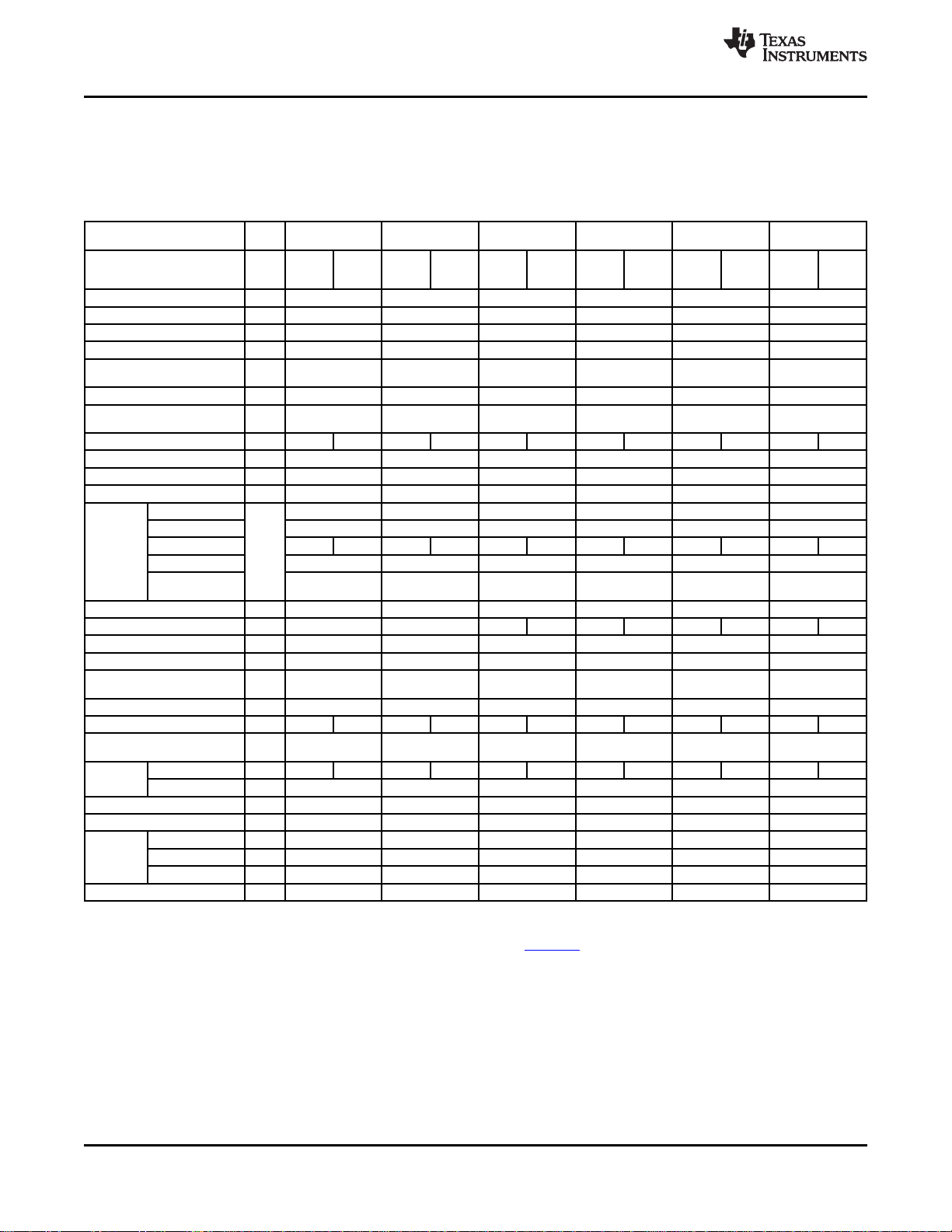
Table 2-1 lists the features of the TMS320F2803x devices.
Table 2-1. Hardware Features
FEATURE TYPE
Package Type PAG PN PAG PN PAG PN PAG PN PAG PN PAG PN
Instruction cycle – 16.67 ns 16.67 ns 16.67 ns 16.67 ns 16.67 ns 16.67 ns
Control Law Accelerator 0 No No No Yes No Yes
On-chip flash (16-bitword) – 16K 32K 32K 32K 64K 64K
On-chip SARAM (16-bitword) – 6K 8K 10K 10K 10K 10K
Code security foron-chip
flash/SARAM/OTP blocks
Boot ROM (8Kx 16) – Yes Yes Yes Yes Yes Yes
One-time programmable (OTP)ROM
(16-bit word)
ePWM outputs 1 12 14 12 14 12 14 12 14 12 14 12 14
eCAP inputs 0 1 1 1 1 1 1
eQEP modules 0 1 1 1 1 1 1
Watchdog timer – Yes Yes Yes Yes Yes Yes
MSPS 2.0 2.0 4.6 4.6 4.6 4.6
Conversion Time 500.00 ns 500.00 ns 216.67 ns 216.67ns 216.67 ns 216.67 ns
12-Bit ADC 3
32-Bit CPU timers – 3 3 3 3 3 3
HiRES ePWM Channels 1 – – 6 7 6 7 6 7 6 7
Comparators with IntegratedDACs 0 3 3 3 3 3 3
Inter-integrated circuit (I2C) 0 1 1 1 1 1 1
Enhanced Controller AreaNetwork
(eCAN)
Local Interconnect Network(LIN) 0 1 1 1 1 1 1
Serial Peripheral Interface(SPI) 1 1 2 1 2 1 2 1 2 1 2 1 2
Serial Communications Interface
(SCI)
I/O pins
(shared)
External interrupts – 3 3 3 3 3 3
Supply voltage (nominal) – 3.3 V 3.3 V 3.3 V 3.3 V 3.3 V 3.3 V
Temperature
options
Product status
Channels 14 16 14 16 14 16 14 16 14 16 14 16
Temperature Sensor Yes Yes Yes Yes Yes Yes
Dual
Sample-and-Hold
GPIO – 33 45 33 45 33 45 33 45 33 45 33 45
AIO – 6 6 6 6 6 6
T: –40°C to 105°C – Yes Yes Yes Yes Yes Yes
S: –40°C to 125°C – Yes Yes Yes Yes Yes Yes
Q: –40°C to 125°C
(3)
(1)
– Yes Yes Yes Yes Yes Yes
– 1K 1K 1K 1K 1K 1K
0 1 1 1 1 1 1
0 1 1 1 1 1 1
(2)
– Yes Yes Yes Yes Yes Yes
– TMS TMS TMS TMS TMS TMS
(1) A type change represents a major functional feature difference in a peripheral module. Within a peripheral type, there may be minor
differences between devices that do not affect the basic functionality of the module. These device-specific differences are listed in the
TMS320x28xx, 28xxx DSP Peripheral Reference Guide (literature number SPRU566) and in the peripheral reference guides.
(2) "Q" refers to Q100 qualification for automotive applications.
(3) See Section 5.1 , Device and Development Support Tool Nomenclature, for descriptions of device stages. The "TMS" product status
denotes a fully qualified production device.
28030 28031 28032 28033 28034 28035
(60 MHz) (60 MHz) (60 MHz) (60 MHz) (60 MHz) (60 MHz)
64-Pin 80-Pin 64-Pin 80-Pin 64-Pin 80-Pin 64-Pin 80-Pin 64-Pin 80-Pin 64-Pin 80-Pin
TQFP LQFP TQFP LQFP TQFP LQFP TQFP LQFP TQFP LQFP TQFP LQFP
Yes Yes Yes Yes Yes Yes
4 Introduction Copyright © 2009–2010, Texas Instruments Incorporated
Submit Documentation Feedback
Product Folder Link(s): TMS320F28030 TMS320F28031 TMS320F28032 TMS320F28033 TMS320F28034
TMS320F28035
Page 5
33
16
48
1
49
64
17
32
2
3
4
5
6
7
8
9
10
11
12
13
14
15
18
19
20
21
22
23
24
25
26
27
28
29
30
31
GPIO18/SPICLKA/LINTXA/XCLKOUT
GPIO36/TMS
GPIO35/TDI
GPIO37/TDO
GPIO38/TCK/XCLKIN
GPIO19/XCLKIN/ /LINRXA/ECAP1SPISTEA
V
DD
VSSX1
X2
GPIO6/EPWM4A/EPWMSYNCI/EPWMSYNCO
GPIO7/EPWM4B/SCIRXDA
GPIO12/ /SCITXDATZ1
GPIO16/SPISIMOA/TZ2
GPIO8/EPWM5A/ADCSOCAO
GPIO17/SPISOMIA/TZ3
GPIO24/ECAP1
GPIO11/EPWM6B/LINRXA
GPIO21/EQEP1B/COMP2OUT
GPIO20/EQEP1A/COMP1OUT
GPIO34/COMP2OUT/COMP3OUT
V
REGENZ
V
DD
V
SS
V
DDIO
GPIO0/EPWM1A
GPIO1/EPWM1B/COMP1OUT
GPIO2/EPWM2A
GPIO3/EPWM2B/SPISOMIA/COMP2OUT
GPIO10/EPWM6A/ADCSOCBO
GPIO4/EPWM3A
GPIO5/EPWM3B/SPSIMOA/ECAP1
34
35
36
37
38
39
40
41
42
43
44
45
46
47
V
DDA
GPIO22/EQEP1S/LINTXA
ADCINA0/VREFHI
ADCINA1
ADCINA2/COMP1A/AIO2
ADCINA3
ADCINA4/COMP2A/AIO4
ADCINA6/COMP3A/AIO6
ADCINA7
TRST
XRS
V
SS
V
DD
GPIO23/EQEP1I/LINRXA
GPIO33/SCLA/EPWMSYNCO/ADCSOCBO
GPIO32/SDAA/EPWMSYNCI/ADCSOCAO
50
51
52
53
54
55
56
57
58
59
60
61
62
63
GPIO28/SCIRXDA/SDAA/TZ2
V /V
SSA REFLO
GPIO9/EPWM5B/LINTXA
TEST2
V
DDIO
V
SS
GPIO29/SCITXDA/SCLA/TZ3
GPIO30/CANRXA
GPIO31/CANTXA
ADCINB7
ADCINB6/COMP3B/AIO14
ADCINB4/COMP2B/AIO12
ADCINB3
ADCINB2/COMP1B/AIO10
ADCINB1
ADCINB0
TMS320F28030, TMS320F28031, TMS320F28032
TMS320F28033, TMS320F28034, TMS320F28035
www.ti.com
SPRS584D–APRIL 2009–REVISED JUNE 2010
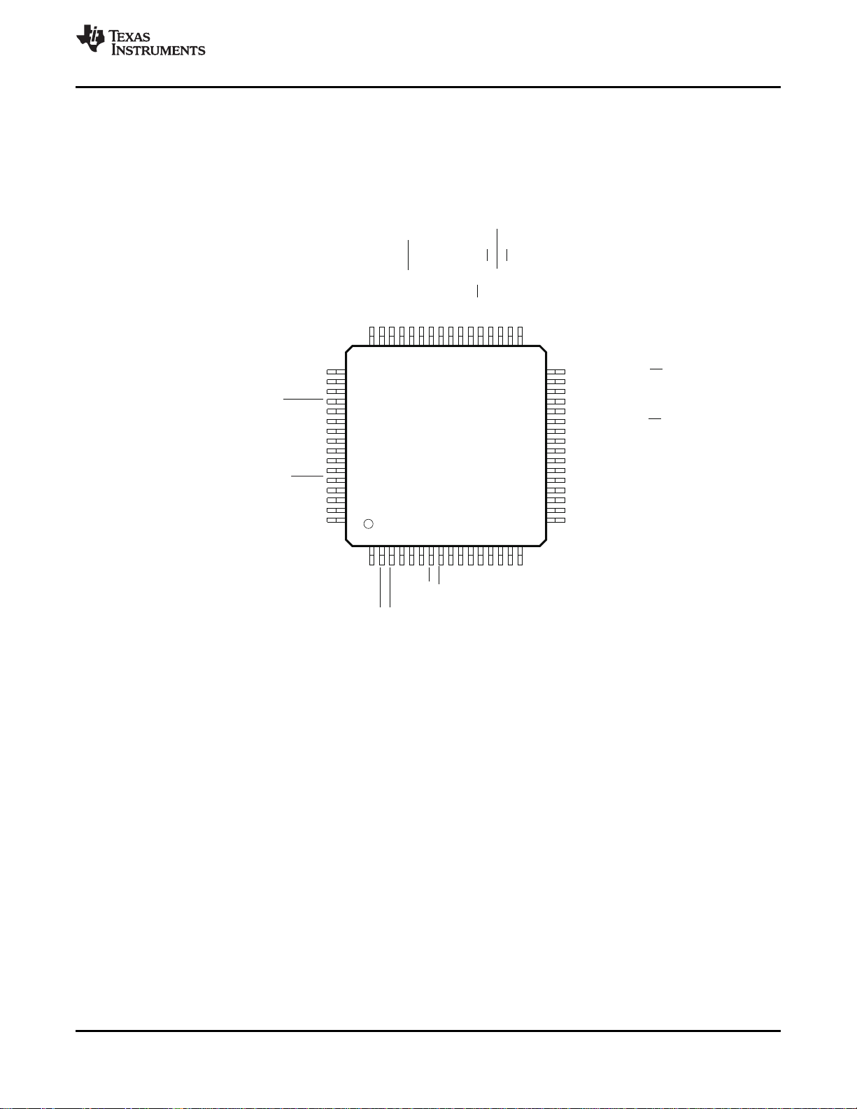
2.1 Pin Assignments
Figure 2-1 shows the 64-pin PAG Thin Quad Flatpack (TQFP) pin assignments. Figure 2-2 shows the
80-pin PN Low-Profile Quad Flatpack (LQFP) pin assignments.
A. Pin 15: VREFHI and ADCINA0 share the same pin on the 64-pin PAG device and their use is mutually exclusive to
B. Pin 17: VREFLO is always connected to V
Copyright © 2009–2010, Texas Instruments Incorporated Introduction 5
one another.
Figure 2-1. 2803x 64-Pin PAG TQFP (Top View)
SSA
Submit Documentation Feedback
on the 64-pin PAG device.
Product Folder Link(s): TMS320F28030 TMS320F28031 TMS320F28032 TMS320F28033 TMS320F28034
TMS320F28035
Page 6
20
1
2
3
4
5
6
7
8
9
10
11
12
13
14
15
16
17
18
19
41
60
59
58
57
56
55
54
53
52
51
50
49
48
47
46
45
44
43
42
21
40
39
38
37
36
35
34
33
32
31
30
29
28
27
26
25
24
23
22
80
61
62
63
64
65
66
67
68
69
70
71
72
73
74
75
76
77
78
79
V
SSA
GPIO28/SCIRXDA/SDAA/TZ2
GPIO9/EPWM5B/LINTXA
TEST2
GPIO26/SPICLKB
V
DDIO
V
SS
GPIO29/SCITXDA/SCLA/TZ3
GPIO30/CANRXA
GPIO31/CANTXA
GPIO27/SPISTEB
ADCINB7
ADCINB6/COMP3B/AIO14
ADCINB5
ADCINB4/COMP2B/AIO12
ADCINB3
ADCINB2/COMP1B/AIO10
ADCINB1
ADCINB0
V
REFLO
GPIO24/ECAP1/SPISIMOB
GPIO11/EPWM6B/LINRXA
GPIO5/EPWM3B/SPISIMOA/ECAP1
GPIO4/EPWM3A
GPIO40/EPWM7A
GPIO10/EPWM6A/ADCSOCBO
GPIO3/EPWM2B/SPISOMIA/COMP2OUT
GPIO2/EPWM2A
GPIO1/EPWM1B/COMP1OUT
GPIO0/EPWM1A
V
DDIO
V
SS
V
DD
V
REGENZ
GPIO34/COMP2OUT/COMP3OUT
GPIO15/ /LINRXA/TZ1 SPISTEB
GPIO13/ /SPISOMIBTZ2
GPIO14/ /LINTXA/SPICLKBTZ3
GPIO20/EQEP1A/COMP1OUT
GPIO21/EQEP1B/COMP2OUT
V
DDA
GPIO22/EQEP1S/LINTXA
GPIO32/SDAA/EPWMSYNCI/ADCSOCAO
GPIO33/SCLA/EPWMSYNCO/ADCSOCBO
GPIO23/EQEP1I/LINRXA
GPIO42/COMP1OUT
GPIO43/COMP2OUT
V
DD
V
SS
XRS
TRST
ADCINA7
ADCINA6/COMP3A/AIO6
ADCINA5
ADCINA4/COMP2A/AIO4
ADCINA3
ADCINA2/COMP1A/AIO2
ADCINA1
ADCINA0
V
REFHI
GPIO18/SPICLKA/LINTXA/XCLKOUT
GPIO36/TMS
GPIO35/TDI
GPIO37/TDO
GPIO38/TCK/XCLKIN
GPIO39
GPIO19/XCLKIN/ /LINRXA/ECAP1SPISTEA
VDDVSSX1
X2
GPIO6/EPWM4A/EPWMSYNCI/EPWMSYNCO
GPIO7/EPWM4B/SCIRXDA
GPIO41/EPWM7B
GPIO12/ /SCITXDA/SPISIMOBTZ1
GPIO16/SPISIMOA/TZ2
GPIO44
GPIO25/SPISOMIB
GPIO8/EPWM5A/ADCSOCAO
GPIO17/SPISOMIA/TZ3
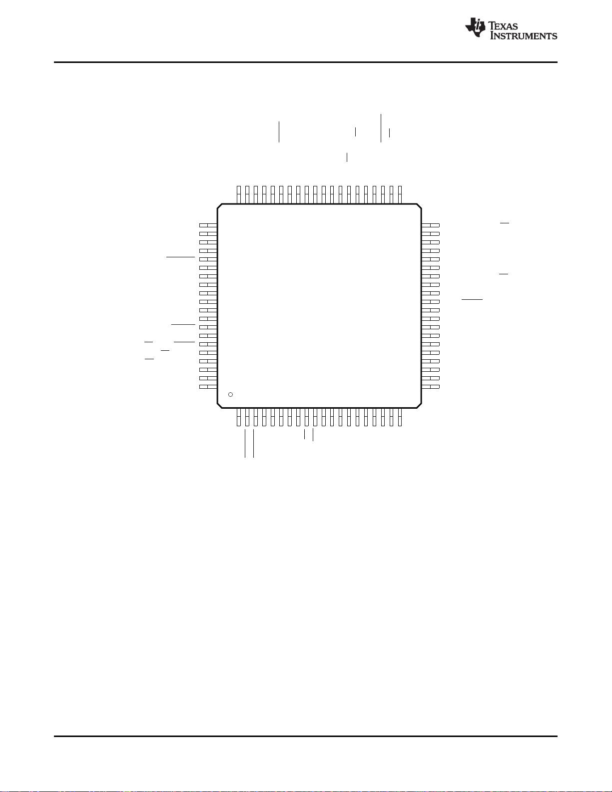
TMS320F28030, TMS320F28031, TMS320F28032
TMS320F28033, TMS320F28034, TMS320F28035
SPRS584D–APRIL 2009–REVISED JUNE 2010
www.ti.com
Figure 2-2. 2803x 80-Pin PN LQFP (Top View)
6 Introduction Copyright © 2009–2010, Texas Instruments Incorporated
Submit Documentation Feedback
Product Folder Link(s): TMS320F28030 TMS320F28031 TMS320F28032 TMS320F28033 TMS320F28034
TMS320F28035
Page 7
TMS320F28030, TMS320F28031, TMS320F28032
TMS320F28033, TMS320F28034, TMS320F28035
www.ti.com
SPRS584D–APRIL 2009–REVISED JUNE 2010
2.2 Signal Descriptions
Table 2-2 describes the signals. With the exception of the JTAG pins, the GPIO function is the default at
reset, unless otherwise mentioned. The peripheral signals that are listed under them are alternate
functions. Some peripheral functions may not be available in all devices. See Table 2-1 for details. Inputs
are not 5-V tolerant. All GPIO pins are I/O/Z and have an internal pullup, which can be selectively
enabled/disabled on a per-pin basis. This feature only applies to the GPIO pins. The pullups on the PWM
pins are not enabled at reset. The pullups on other GPIO pins are enabled upon reset. The AIO pins do
not have an internal pullup.
Table 2-2. Terminal Functions
TERMINAL
NAME
TRST 10 8 I normal device operation. An external pull-down resistor is required on this pin. The
TCK See GPIO38 I See GPIO38. JTAG test clock with internal pullup (↑)
TMS See GPIO36 I
TDI See GPIO35 I
TDO See GPIO37 O/Z register (instruction or data) are shifted out of TDO on the falling edge of TCK. (8 mA
TEST2 38 30 I/O Test Pin. Reserved for TI. Must be left unconnected.
XCLKOUT See GPIO18 O/Z
XCLKIN I path must be disabled by bit 13 in the CLKCTL register.
X1 52 41 I
X2 51 40 O
PN PAG
PIN # PIN #
See GPIO19 and
GPIO38
I/O/Z DESCRIPTION
JTAG
JTAG test reset with internal pulldown. TRST, when driven high, gives the scan
system control of the operations of the device. If this signal is not connected or driven
low, the device operates in its functional mode, and the test reset signals are ignored.
NOTE: TRST is an active high test pin and must be maintained low at all times during
value of this resistor should be based on drive strength of the debugger pods
applicable to the design. A 2.2-kΩ resistor generally offers adequate protection. Since
this is application-specific, it is recommended that each target board be validated for
proper operation of the debugger and the application. (↓)
See GPIO36. JTAG test-mode select (TMS) with internal pullup. This serial control
input is clocked into the TAP controller on the rising edge of TCK. (↑)
See GPIO35. JTAG test data input (TDI) with internal pullup. TDI is clocked into the
selected register (instruction or data) on a rising edge of TCK. (↑)
See GPIO37. JTAG scan out, test data output (TDO). The contents of the selected
drive)
FLASH
CLOCK
See GPIO18. Output clock derived from SYSCLKOUT. XCLKOUT is either the same
frequency, one-half the frequency, or one-fourth the frequency of SYSCLKOUT. This
is controlled by bits 1:0 (XCLKOUTDIV) in the XCLK register. At reset, XCLKOUT =
SYSCLKOUT/4. The XCLKOUT signal can be turned off by setting XCLKOUTDIV
to 3. The mux control for GPIO18 must also be set to XCLKOUT for this signal to
propogate to the pin.
See GPIO19 and GPIO38. External oscillator input. Pin source for the clock is
controlled by the XCLKINSEL bit in the XCLK register, GPIO38 is the default
selection. This pin feeds a clock from an external 3.3-V oscillator. In this case, the X1
pin, if available, must be tied to GND and the on-chip crystal oscillator must be
disabled via bit 14 in the CLKCTL register. If a crystal/resonator is used, the XCLKIN
NOTE: Designs that use the GPIO38/TCK/XCLKIN pin to supply an external clock for
normal device operation may need to incorporate some hooks to disable this path
during debug using the JTAG connector. This is to prevent contention with the TCK
signal, which is active during JTAG debug sessions. The zero-pin internal oscillators
may be used during this time to clock the device.
On-chip crystal-oscillator input. To use this oscillator, a quartz crystal or a ceramic
resonator must be connected across X1 and X2. In this case, the XCLKIN path must
be disabled by bit 13 in the CLKCTL register. If this pin is not used, it must be tied to
GND. (I)
On-chip crystal-oscillator output. A quartz crystal or a ceramic resonator must be
connected across X1 and X2. If X2 is not used, it must be left unconnected. (O)
(1)
(1) I = Input, O = Output, Z = High Impedance, OD = Open Drain, ↑ = Pullup, ↓ = Pulldown
Copyright © 2009–2010, Texas Instruments Incorporated Introduction 7
Submit Documentation Feedback
Product Folder Link(s): TMS320F28030 TMS320F28031 TMS320F28032 TMS320F28033 TMS320F28034
TMS320F28035
Page 8
TMS320F28030, TMS320F28031, TMS320F28032
TMS320F28033, TMS320F28034, TMS320F28035
SPRS584D–APRIL 2009–REVISED JUNE 2010
Table 2-2. Terminal Functions
TERMINAL
NAME
XRS 9 7 I/O
ADCINA7 11 9 I ADC Group A, Channel 7 input
ADCINA6 ADC Group A, Channel 6 input
COMP3A 12 10 Comparator Input 3A
AIO6 Digital AIO 6
ADCINA5 13 –
ADCINA4 I ADC Group A, Channel 4 input
COMP2A 14 11 I Comparator Input 2A
AIO4 I/O Digital AIO 4
ADCINA3 15 12 I ADC Group A, Channel 3 input
ADCINA2 I ADC Group A, Channel 2 input
COMP1A 16 13 I Comparator Input 1A
AIO2 I/O Digital AIO 2
ADCINA1 17 14 I ADC Group A, Channel 1 input
ADCINA0 18 15 I NOTE: VREFHI and ADCINA0 share the same pin on the 64-pin PAG device and their
VREFHI 19 15
ADCINB7 30 24 I ADC Group B, Channel 7 input
ADCINB6 ADC Group B, Channel 6 input
COMP3B 29 23 Comparator Input 3B
AIO14 Digital AIO 14
ADCINB5 28 –
ADCINB4 I ADC Group B, Channel 4 input
COMP2B 27 22 I Comparator Input 2B
AIO12 I/O Digital AIO12
ADCINB3 26 21 I ADC Group B, Channel 3 input
ADCINB2 I ADC Group B, Channel 2 input
COMP1B 25 20 I Comparator Input 1B
AIO10 I/O Digital AIO 10
ADCINB1 24 19 I ADC Group B, Channel 1 input
ADCINB0 23 18
VREFLO 22 17 NOTE: VREFLO is always connected to V
PN PAG
PIN # PIN #
I/O/Z DESCRIPTION
RESET
Device Reset (in) and Watchdog Reset (out). Piccolo devices have a built-in
power-on-reset (POR) and brown-out-reset (BOR) circuitry. As such, no external
circuitry is needed to generate a reset pulse. During a power-on or brown-out
condition, this pin is driven low by the device. See the electrical section for thresholds
of the POR/BOR block. This pin is also driven low by the MCU when a watchdog reset
occurs. During watchdog reset, the XRS pin is driven low for the watchdog reset
duration of 512 OSCCLK cycles. If need be, an external circuitry may also drive this
pin to assert a device reset. In this case, it is recommended that this pin be driven by
an open-drain device. An R-C circuit must be connected to this pin for noise immunity
reasons. Regardless of the source, a device reset causes the device to terminate
execution. The program counter points to the address contained at the location
0x3FFFC0. When reset is deactivated, execution begins at the location designated by
the program counter. The output buffer of this pin is an open-drain with an internal
pullup. (I/OD)
ADC, COMPARATOR, ANALOG I/O
I
I/O
ADC Group A, Channel 0 input.
use is mutually exclusive to one another.
ADC External Reference – only used when in ADC external reference mode. See
ADC Section..
NOTE: VREFHI and ADCINA0 share the same pin on the 64-pin PAG device and their
use is mutually exclusive to one another.
I
I/O
(1)
(continued)
on the 64-pin PAG device.
SSA
www.ti.com
8 Introduction Copyright © 2009–2010, Texas Instruments Incorporated
Submit Documentation Feedback
Product Folder Link(s): TMS320F28030 TMS320F28031 TMS320F28032 TMS320F28033 TMS320F28034
TMS320F28035
Page 9
TMS320F28030, TMS320F28031, TMS320F28032
TMS320F28033, TMS320F28034, TMS320F28035
www.ti.com
Table 2-2. Terminal Functions
(1)
(continued)
SPRS584D–APRIL 2009–REVISED JUNE 2010
TERMINAL
NAME
PN PAG
PIN # PIN #
I/O/Z DESCRIPTION
CPU AND I/O POWER
V
V
V
V
V
V
V
V
V
V
V
DDA
SSA
DD
DD
DD
DDIO
DDIO
SS
SS
SS
SS
20 16 Analog Power Pin. Tie with a 2.2-mF capacitor (typical) close to the pin.
21 17
Analog Ground Pin.
NOTE: VREFLO is always connected to V
on the 64-pin PAG device.
SSA
7 5 CPU and Logic Digital Power Pins – no supply source needed when using internal
54 43
72 59
36 29
70 57
VREG. Tie with 1.2 µF (minimum) ceramic capacitor (10% tolerance) to ground when
using internal VREG. Higher value capacitors may be used, but could impact
supply-rail ramp-up time.
Digital I/O and Flash Power Pin – Single Supply source when VREG is enabled
8 6
35 28
53 42
Digital Ground Pins
71 58
VOLTAGE REGULATOR CONTROL SIGNAL
VREGENZ 73 60 I Internal VREG Enable/Disable – pull low to enable VREG, pull high to disable VREG
GPIO AND PERIPHERAL SIGNALS
(1)
GPIO0 69 56 I/O/Z General purpose input/output 0
EPWM1A O Enhanced PWM1 Output A and HRPWM channel
– – –
– – –
GPIO1 68 55 I/O/Z General purpose input/output 1
EPWM1B O Enhanced PWM1 Output B
– –
COMP1OUT O Direct output of Comparator 1
GPIO2 67 54 I/O/Z General purpose input/output 2
EPWM2A O Enhanced PWM2 Output A and HRPWM channel
– –
– –
GPIO3 66 53 I/O/Z General purpose input/output 3
EPWM2B O Enhanced PWM2 Output B
SPISOMIA I/O SPI-A slave out, master in
COMP2OUT O Direct output of Comparator 2
GPIO4 63 51 I/O/Z General purpose input/output 4
EPWM3A O Enhanced PWM3 output A and HRPWM channel
– –
– –
GPIO5 62 50 I/O/Z General purpose input/output 5
EPWM3B O Enhanced PWM3 output B
SPISIMOA I/O SPI-A slave in, master out
ECAP1 I/O Enhanced Capture input/output 1
(1) The GPIO function (shown in bold italics) is the default at reset. The peripheral signals that are listed under them are alternate functions.
For JTAG pins that have the GPIO functionality multiplexed, the input path to the GPIO block is always valid. The output path from the
GPIO block and the path to the JTAG block from a pin is enabled/disabled based on the condition of the TRST signal. See the
TMS320x2803x Piccolo System Control and Interrupts Reference Guide (literature number SPRUGL8) for details.
Copyright © 2009–2010, Texas Instruments Incorporated Introduction 9
Submit Documentation Feedback
Product Folder Link(s): TMS320F28030 TMS320F28031 TMS320F28032 TMS320F28033 TMS320F28034
TMS320F28035
Page 10

TMS320F28030, TMS320F28031, TMS320F28032
TMS320F28033, TMS320F28034, TMS320F28035
SPRS584D–APRIL 2009–REVISED JUNE 2010
Table 2-2. Terminal Functions
TERMINAL
NAME
GPIO6 50 39 I/O/Z General purpose input/output 6
EPWM4A O Enhanced PWM4 output A and HRPWM channel
EPWMSYNCI I External ePWM sync pulse input
EPWMSYNCO O External ePWM sync pulse output
GPIO7 49 38 I/O/Z General purpose input/output 7
EPWM4B O Enhanced PWM4 output B
SCIRXDA I SCI-A receive data
– –
GPIO8 43 35 I/O/Z General purpose input/output 8
EPWM5A O Enhanced PWM5 output A and HRPWM channel
– –
ADCSOCAO O ADC start-of-conversion A
GPIO9 39 31 I/O/Z General purpose input/output 9
EPMW5B O Enhanced PWM5 output B
LINTXA LIN transmit A
– –
GPIO10 65 52 I/O/Z General purpose input/output 10
EPWM6A O Enhanced PWM6 output A and HRPWM channel
– –
ADCSOCBO O ADC start-of-conversion B
GPIO11 61 49 I/O/Z General purpose input/output 11
EPWM6B Enhanced PWM6 output B
LINRXA LIN receive A
– –
GPIO12 47 37 I/O/Z General purpose input/output 12
TZ1 I Trip Zone input 1
SCITXDA O SCI-A transmit data
SPISIMOB I/O SPI-B slave in, master out.
GPIO13 76 – I/O/Z General purpose input/output 13
TZ2 I Trip Zone input 2
SPISOMIB I/O SPI-B slave out, master in
– –
GPIO14 77 – I/O/Z General purpose input/output 14
TZ3 I Trip zone input 3
LINTXA O LIN transmit
SPICLKB I/O SPI-B clock input/output
GPIO15 75 – I/O/Z General purpose input/output 15
TZ1 I Trip zone input 1
LINRXA I LIN receive
SPISTEB I/O SPI-B slave transmit enable input/output
PN PAG
PIN # PIN #
I/O/Z DESCRIPTION
NOTE: The SPI-B peripheral is only available in the PN package.
(1)
(continued)
www.ti.com
10 Introduction Copyright © 2009–2010, Texas Instruments Incorporated
Submit Documentation Feedback
Product Folder Link(s): TMS320F28030 TMS320F28031 TMS320F28032 TMS320F28033 TMS320F28034
TMS320F28035
Page 11

TMS320F28030, TMS320F28031, TMS320F28032
TMS320F28033, TMS320F28034, TMS320F28035
www.ti.com
Table 2-2. Terminal Functions
TERMINAL
NAME
GPIO16 46 36 I/O/Z General purpose input/output 16
SPISIMOA I/O SPI-A slave in, master out
– –
TZ2 I Trip Zone input 2
GPIO17 42 34 I/O/Z General purpose input/output 17
SPISOMIA I/O SPI-A slave out, master in
– –
TZ3 I Trip zone input 3
GPIO18 41 33 I/O/Z General purpose input/output 18
SPICLKA I/O SPI-A clock input/output
LINTXA O LIN transmit
XCLKOUT O/Z Output clock derived from SYSCLKOUT. XCLKOUT is either the same frequency,
GPIO19 55 44 I/O/Z General purpose input/output 19
XCLKIN External Oscillator Input. The path from this pin to the clock block is not gated by the
SPISTEA I/O SPI-A slave transmit enable input/output
LINRXA I LIN receive
ECAP1 I/O Enhanced Capture input/output 1
GPIO20 78 62 I/O/Z General purpose input/output 20
EQEP1A I Enhanced QEP1 input A
– –
COMP1OUT O Direct output of Comparator 1
GPIO21 79 63 I/O/Z General purpose input/output 21
EQEP1B I Enhanced QEP1 input B
– –
COMP2OUT O Direct output of Comparator 2
GPIO22 1 1 I/O/Z General purpose input/output 22
EQEP1S I/O Enhanced QEP1 strobe
LINTXA O LIN transmit
– –
GPIO23 4 4 I/O/Z General purpose input/output 23
EQEP1I I/O Enhanced QEP1 index
LINRXA I LIN receive
– –
GPIO24 80 64 I/O/Z General purpose input/output 24
ECAP1 I/O Enhanced Capture input/output 1
SPISIMOB I/O SPI-B slave in, master out.
– –
PN PAG
PIN # PIN #
I/O/Z DESCRIPTION
one-half the frequency, or one-fourth the frequency of SYSCLKOUT. This is controlled
by bits 1:0 (XCLKOUTDIV) in the XCLK register. At reset, XCLKOUT =
SYSCLKOUT/4. The XCLKOUT signal can be turned off by setting XCLKOUTDIV
to 3. The mux control for GPIO18 must also be set to XCLKOUT for this signal to
propogate to the pin.
mux function of this pin. Care must be taken not to enable this path for clocking if it is
being used for the other periperhal functions
NOTE: The SPI-B peripheral is only available in the PN package.
(1)
(continued)
SPRS584D–APRIL 2009–REVISED JUNE 2010
Copyright © 2009–2010, Texas Instruments Incorporated Introduction 11
Submit Documentation Feedback
Product Folder Link(s): TMS320F28030 TMS320F28031 TMS320F28032 TMS320F28033 TMS320F28034
TMS320F28035
Page 12

TMS320F28030, TMS320F28031, TMS320F28032
TMS320F28033, TMS320F28034, TMS320F28035
SPRS584D–APRIL 2009–REVISED JUNE 2010
Table 2-2. Terminal Functions
TERMINAL
NAME
GPIO25 44 – I/O/Z General purpose input/output 25
– –
SPISOMIB I/O SPI-B slave out , master in
– –
GPIO26 37 – I/O/Z General purpose input/output 26
– –
SPICLKB I/O SPI-B clock input/output
– –
GPIO27 31 – I/O/Z General purpose input/output 27
– –
SPISTEB I/O SPI-B slave transmit enable input/output
– –
GPIO28 40 32 I/O/Z General purpose input/output 28
SCIRXDA I SCI receive data
SDAA I/OD I2C data open-drain bidirectional port
TZ2 I Trip zone input 2
GPIO29 34 27 I/O/Z General purpose input/output 2
SCITXDA O SCI transmit data
SCLA I/OD I2C clock open-drain bidirectional port
TZ3 I Trip zone input 3
GPIO30 33 26 I/O/Z General purpose input/output 30
CANRXA I CAN receive
– –
– –
GPIO31 32 25 I/O/Z General purpose input/output 31
CANTXA O CAN transmit
– –
– –
GPIO32 2 2 I/O/Z General purpose input/output 32
SDAA I/OD I2C data open-drain bidirectional port
EPWMSYNCI I Enhanced PWM external sync pulse input
ADCSOCAO O ADC start-of-conversion A
GPIO33 3 3 I/O/Z General-Purpose Input/Output 33
SCLA I/OD I2C clock open-drain bidirectional port
EPWMSYNCO O Enhanced PWM external synch pulse output
ADCSOCBO O ADC start-of-conversion B
GPIO34 74 61 I/O/Z General-Purpose Input/Output 34
COMP2OUT O Direct output of Comparator 2
COMP3OUT O Direct output of Comparator 3
– –
GPIO35 59 47 I/O/Z General-Purpose Input/Output 35
TDI I JTAG test data input (TDI) with internal pullup. TDI is clocked into the selected register
GPIO36 60 48 I/O/Z General-Purpose Input/Output 36
TMS I JTAG test-mode select (TMS) with internal pullup. This serial control input is clocked
PN PAG
PIN # PIN #
I/O/Z DESCRIPTION
(instruction or data) on a rising edge of TCK
into the TAP controller on the rising edge of TCK.
(1)
(continued)
www.ti.com
12 Introduction Copyright © 2009–2010, Texas Instruments Incorporated
Submit Documentation Feedback
Product Folder Link(s): TMS320F28030 TMS320F28031 TMS320F28032 TMS320F28033 TMS320F28034
TMS320F28035
Page 13

TMS320F28030, TMS320F28031, TMS320F28032
TMS320F28033, TMS320F28034, TMS320F28035
www.ti.com
Table 2-2. Terminal Functions
TERMINAL
NAME
GPIO37 58 46 I/O/Z General-Purpose Input/Output 37
TDO O/Z JTAG scan out, test data output (TDO). The contents of the selected register
GPIO38 57 45 I/O/Z General-Purpose Input/Output 38
TCK I JTAG test clock with internal pullup
XCLKIN I External Oscillator Input. The path from this pin to the clock block is not gated by the
– –
GPIO39 56 – I/O/Z General-Purpose Input/Output 39
– –
– –
– –
GPIO40 64 – I/O/Z General-Purpose Input/Output 40
EPWM7A O Enhanced PWM7 output A and HRPWM channel
– –
– –
GPIO41 48 – I/O/Z General-Purpose Input/Output 41
EPWM7B O Enhanced PWM7 output B
– –
– –
GPIO42 5 – I/O/Z General-Purpose Input/Output 42
COMP1OUT O Direct output of Comparator 1
– –
– –
GPIO43 6 – I/O/Z General-Purpose Input/Output 43
COMP2OUT O Direct output of Comparator 2
– –
– –
GPIO44 45 – I/O/Z General-Purpose Input/Output 44
– –
– –
– –
PN PAG
PIN # PIN #
I/O/Z DESCRIPTION
(instruction or data) are shifted out of TDO on the falling edge of TCK (8 mA drive)
mux function of this pin. Care must be taken to not enable this path for clocking if it is
being used for the other functions.
(1)
(continued)
SPRS584D–APRIL 2009–REVISED JUNE 2010
Copyright © 2009–2010, Texas Instruments Incorporated Functional Overview 13
Submit Documentation Feedback
Product Folder Link(s): TMS320F28030 TMS320F28031 TMS320F28032 TMS320F28033 TMS320F28034
TMS320F28035
Page 14
3ExternalInterrupts
M0
SARAM1Kx16
(0-wait)
16-bitPeripheralBus
SPISTEx
M1
SARAM1Kx16
(0-wait)
eCAN
(32-mail
box)
SCI
(4L FIFO)
ePWM
SPI
(4L FIFO)
I2C
(4L FIFO)
LIN
HRPWM
eCAP
32-BitPeripheralBus
GPIOMUX
C28x
32-bitCPU
A7:0
B7:0
PIE
CPUTimer0
CPUTimer1
CPUTimer2
TCK
TDI
TMS
TDO
TRST
OSC1,
OSC2,
Ext,
PLL,
LPM,
WD
XCLKIN
X2
XRS
32-bitPeripheralBus
(CLA accessible)
ECA Px
EP W MxA
EP W MxB
ES Y NCI
ES YN CO
CA NT Xx
CA NR Xx
SDA x
SC Lx
SP IS IMO x
SP IS OMI x
SP IC LKx
COMP1OUT
SCI RXDx
GPIO
Mux
LPMWakeup
CLA
ADC
PSWD
FLASH
32K/64Kx16
Secure
OTP/Flash
Wrapper
Boot-ROM
8Kx16
(0-wait)
SARAM
8Kx16
(0-wait)
Secure
L INA RX
LI NAT X
COMP
32- bit pe riph era l b us
( CL A a cces sibl e)
COMP1A
COMP1B
COMP2A
COMP2B
COMP3A
COMP3B
COMP2OUT
COMP3OUT
eQEP
EQ EPx A
EQ EPx B
EQ E PxI
EQ EP xS
SC ITXD x
X1
GPIO
MUX
AIO
MUX
VREG
OTP 1Kx16
Secure
(CLA Onlyon6K)
From
COMP1OUT,
COMP2OUT,
COMP3OUT
POR/
BOR
MemoryBus
CLA Bus
MemoryBus
MemoryBus
TZx
Code
Security
Module
TMS320F28030, TMS320F28031, TMS320F28032
TMS320F28033, TMS320F28034, TMS320F28035
SPRS584D–APRIL 2009–REVISED JUNE 2010
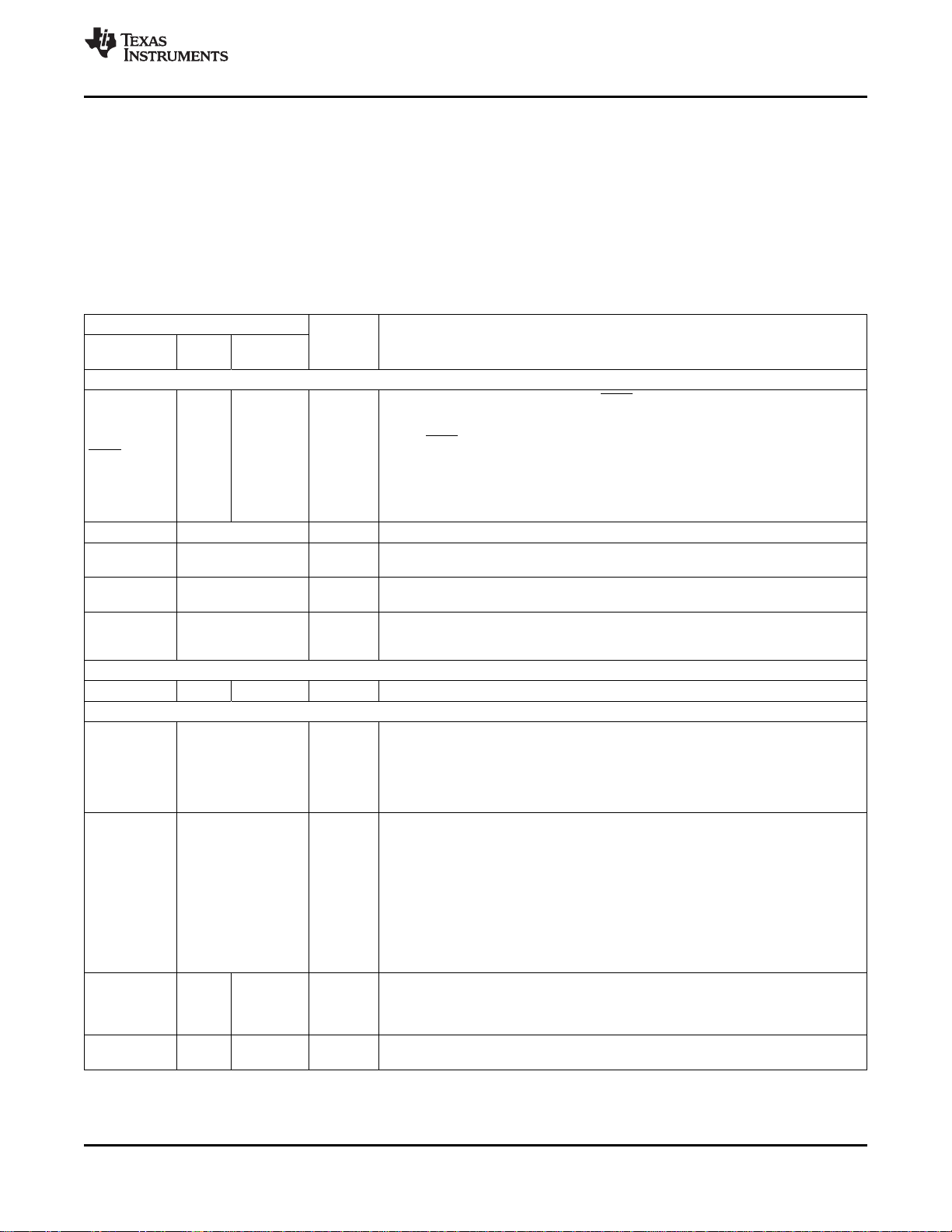
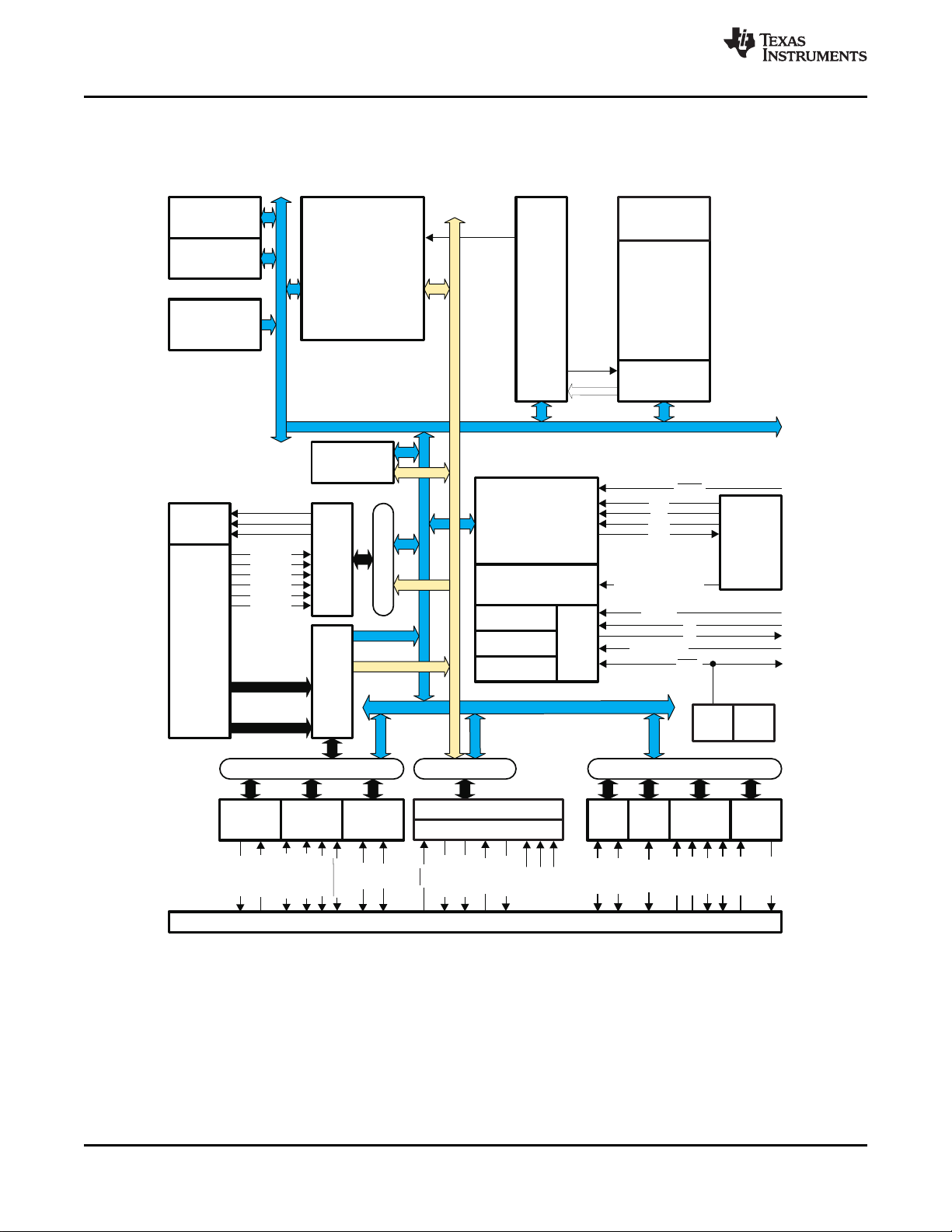
3 Functional Overview
3.1 Block Diagram
www.ti.com
A. Not all peripheral pins are available at the same time due to multiplexing.
Figure 3-1. Functional Block Diagram
14 Functional Overview Copyright © 2009–2010, Texas Instruments Incorporated
Product Folder Link(s): TMS320F28030 TMS320F28031 TMS320F28032 TMS320F28033 TMS320F28034
Submit Documentation Feedback
TMS320F28035
Page 15

TMS320F28030, TMS320F28031, TMS320F28032
TMS320F28033, TMS320F28034, TMS320F28035
www.ti.com
SPRS584D–APRIL 2009–REVISED JUNE 2010
3.2 Memory Maps
In Figure 3-2 through Figure 3-5, the following apply:
• Memory blocks are not to scale.
• Peripheral Frame 0, Peripheral Frame 1 and Peripheral Frame 2 memory maps are restricted to data
memory only. A user program cannot access these memory maps in program space.
• Protected means the order of Write-followed-by-Read operations is preserved rather than the pipeline
order.
• Certain memory ranges are EALLOW protected against spurious writes after configuration.
• Locations 0x3D7C80 – 0x3D7CC0 contain the internal oscillator and ADC calibration routines. These
locations are not programmable by the user.
Copyright © 2009–2010, Texas Instruments Incorporated Functional Overview 15
Submit Documentation Feedback
Product Folder Link(s): TMS320F28030 TMS320F28031 TMS320F28032 TMS320F28033 TMS320F28034
TMS320F28035
Page 16
M0 Vector RAM (Enabled if VMAP = 0)
M0 SARAM (1K x 16, 0-Wait)
0x00 0000
0x00 0040
M1 SARAM (1K x 16, 0-Wait)
0x00 0400
Data Space Prog Space
Reserved
Peripheral Frame 1
(4K x 16, Protected)
Peripheral Frame 2
(4K x 16, Protected)
0x00 7000
0x00 8000
L0 SARAM (2K x 16)
(0-Wait, Secure Zone + ECSL, Dual Mapped)
0x00 8800
L1 DPSARAM (1K x 16)
(0-Wait, Secure Zone + ECSL, CLA Data RAM 0)
0x00 8C00
L2 DPSARAM (1K x 16)
(0-Wait, Secure Zone + ECSL, CLA Data RAM 1)
0x00 9000
L3 DPSARAM (4K x 16)
(0-Wait, Secure Zone + ECSL, CLA Prog RAM)
0x3D 7800
User OTP (1K x 16, Secure Zone + ECSL)
0x3D 7C80
Calibration Data
0x00 6000
0x00 2000
Reserved
0x00 A000
Reserved
0x3D 7C00
Reserved
Reserved
FLASH
(64K x 16, 8 Sectors, Secure Zone + ECSL)
L0 SARAM (2K x 16)
(0-Wait, Secure Zone + ECSL, Dual Mapped)
128-Bit Password
Boot ROM (8K x 16, 0-Wait)
Vector (32 Vectors, Enabled if VMAP = 1)
0x3E 8000
0x3F 7FF8
0x3F 8000
0x3F 8800
0x3F E000
0x3F FFC0
Reserved
0x3D 8000
Reserved
Peripheral Frame 0
0x00 0800
Peripheral Frame 0
0x00 1580
0x00 0D00
PIE Vector - RAM
(256 x 16)
(Enabled if
VMAP = 1,
ENPIE = 1)
0x3D 7CC0
Get_mode function
0x3D 7CE0
Reserved
0x3D 7FFF
PARTID
0x00 1400
0x00 0E00
0x00 1500
0x00 1480
CPU-to-CLA Message RAM
CLA-to-CPU Message RAM
CLA Registers
Peripheral Frame 0
Calibration Data
Reserved
0x3D 7E80
0x3D 7EB0
TMS320F28030, TMS320F28031, TMS320F28032
TMS320F28033, TMS320F28034, TMS320F28035
SPRS584D–APRIL 2009–REVISED JUNE 2010
A. CLA-specific registers and RAM apply to the 28035 device only.
B. Memory locations 0x3D7E80-0x3D7EAF are reserved in TMX silicon.
16 Functional Overview Copyright © 2009–2010, Texas Instruments Incorporated
Product Folder Link(s): TMS320F28030 TMS320F28031 TMS320F28032 TMS320F28033 TMS320F28034
Figure 3-2. 28034/28035 Memory Map
Submit Documentation Feedback
TMS320F28035
www.ti.com
Page 17
M0 Vector RAM (Enabled if VMAP = 0)
M0 SARAM (1K x 16, 0-Wait)
0x00 0000
0x00 0040
M1 SARAM (1K x 16, 0-Wait)
0x00 0400
Data Space Prog Space
Reserved
Peripheral Frame 1
(4K x 16, Protected)
Peripheral Frame 2
(4K x 16, Protected)
0x00 7000
0x00 8000
L0 SARAM (2K x 16)
(0-Wait, Secure Zone + ECSL, Dual Mapped)
0x00 8800
L1 DPSARAM (1K x 16)
(0-Wait, Secure Zone + ECSL, CLA Data RAM 0)
0x00 8C00
L2 DPSARAM (1K x 16)
(0-Wait, Secure Zone + ECSL, CLA Data RAM 1)
0x00 9000
L3 DPSARAM (4K x 16)
(0-Wait, Secure Zone + ECSL, CLA Prog RAM)
0x3D 7800
User OTP (1K x 16, Secure Zone + ECSL)
0x00 6000
0x00 2000
Reserved
0x00 A000
Reserved
0x3D 7C00
Reserved
Reserved
FLASH
(32K x 16, 8 Sectors, Secure Zone + ECSL)
L0 SARAM (2K x 16)
(0-Wait, Secure Zone + ECSL, Dual Mapped)
128-Bit Password
Boot ROM (8K x 16, 0-Wait)
Vector (32 Vectors, Enabled if VMAP = 1)
0x3D 8000
0x3F 0000
0x3F 7FF8
0x3F 8000
0x3F 8800
0x3F E000
0x3F FFC0
Reserved
Reserved
Peripheral Frame 0
0x00 0800
Peripheral Frame 0
0x00 1580
0x00 0D00
PIE Vector - RAM
(256 x 16)
(Enabled if
VMAP = 1,
ENPIE = 1)
0x3D 7C80
Calibration Data
0x3D 7CC0
Get_mode function
0x3D 7CE0
Reserved
0x3D 7FFF
PARTID
Peripheral Frame 0
0x00 0E00
CLA Registers
0x00 1400
CLA-to-CPU Message RAM
0x00 1480
CPU-to-CLA Message RAM
0x00 1500
0x3D 7E80
Calibration Data
0x3D 7EB0
Reserved
TMS320F28030, TMS320F28031, TMS320F28032
TMS320F28033, TMS320F28034, TMS320F28035
www.ti.com
A. CLA-specific registers and RAM apply to the 28033 device only.
SPRS584D–APRIL 2009–REVISED JUNE 2010
B. Memory locations 0x3D7E80-0x3D7EAF are reserved in TMX silicon.
Copyright © 2009–2010, Texas Instruments Incorporated Functional Overview 17
Product Folder Link(s): TMS320F28030 TMS320F28031 TMS320F28032 TMS320F28033 TMS320F28034
Figure 3-3. 28032/28033 Memory Map
Submit Documentation Feedback
TMS320F28035
Page 18
M0 Vector RAM (Enabled if VMAP = 0)
M0 SARAM (1K x 16, 0-Wait)
0x00 0000
0x00 0040
M1 SARAM (1K x 16, 0-Wait)
0x00 0400
Data Space Prog Space
Reserved
Peripheral Frame 1
(4K x 16, Protected)
Peripheral Frame 2
(4K x 16, Protected)
0x00 7000
0x00 8000
0x00 8800
L1 DPSARAM (1K x 16)
(0-Wait, Secure Zone + ECSL, CLA Data RAM 0)
0x00 8C00
L2 DPSARAM (1K x 16)
(0-Wait, Secure Zone + ECSL, CLA Data RAM 1)
0x00 9000
L3 DPSARAM (2K x 16)
(0-Wait, Secure Zone + ECSL, CLA Prog RAM)
0x3D 7800
User OTP (1K x 16, Secure Zone + ECSL)
0x00 6000
0x00 2000
Reserved
0x00 9800
Reserved
0x3D 7C00
Reserved
Reserved
FLASH
(32K x 16, 8 Sectors, Secure Zone + ECSL)
L0 SARAM (2K x 16)
(0-Wait, Secure Zone + ECSL, Dual Mapped)
128-Bit Password
Boot ROM (8K x 16, 0-Wait)
Vector (32 Vectors, Enabled if VMAP = 1)
0x3D 8000
0x3F 0000
0x3F 7FF8
0x3F 8000
0x3F 8800
0x3F E000
0x3F FFC0
Reserved
Reserved
Peripheral Frame 0
0x00 0800
Peripheral Frame 0
0x00 0E00
0x00 0D00
PIE Vector - RAM
(256 x 16)
(Enabled if
VMAP = 1,
ENPIE = 1)
0x3D 7C80
Calibration Data
0x3D 7CC0
Get_mode function
0x3D 7CE0
Reserved
0x3D 7FFF
PARTID
L0 SARAM (2K x 16)
(0-Wait, Secure Zone + ECSL, Dual-Mapped)
0x3D 7E80
Calibration Data
0x3D 7EB0
Reserved
TMS320F28030, TMS320F28031, TMS320F28032
TMS320F28033, TMS320F28034, TMS320F28035
SPRS584D–APRIL 2009–REVISED JUNE 2010
www.ti.com
A. Memory locations 0x3D7E80-0x3D7EAF are reserved in TMX silicon.
18 Functional Overview Copyright © 2009–2010, Texas Instruments Incorporated
Product Folder Link(s): TMS320F28030 TMS320F28031 TMS320F28032 TMS320F28033 TMS320F28034
Figure 3-4. 28031 Memory Map
Submit Documentation Feedback
TMS320F28035
Page 19
M0 Vector RAM (Enabled if VMAP = 0)
M0 SARAM (1K x 16, 0-Wait)
0x00 0000
0x00 0040
M1 SARAM (1K x 16, 0-Wait)
0x00 0400
Data Space Prog Space
Reserved
Peripheral Frame 1
(4K x 16, Protected)
Peripheral Frame 2
(4K x 16, Protected)
0x00 7000
0x00 8000
0x00 8800
0x00 8C00
0x00 9000
0x3D 7800
User OTP (1K x 16, Secure Zone + ECSL)
0x00 6000
0x00 2000
Reserved
0x00 A000
Reserved
0x3D 7C00
Reserved
Reserved
Reserved
FLASH
(16K x 16, 4 Sectors, Secure Zone + ECSL)
L0 SARAM (2K x 16)
(0-Wait, Secure Zone + ECSL, Dual Mapped)
128-Bit Password
Boot ROM (8K x 16, 0-Wait)
Vector (32 Vectors, Enabled if VMAP = 1)
0x3D 8000
0x3F 4000
0x3F 7FF8
0x3F 8000
0x3F 8800
0x3F E000
0x3F FFC0
Reserved
Reserved
Peripheral Frame 0
0x00 0800
Peripheral Frame 0
0x00 0E00
0x00 0D00
PIE Vector - RAM
(256 x 16)
(Enabled if
VMAP = 1,
ENPIE = 1)
0x3D 7C80
Calibration Data
0x3D 7CC0
Get_mode function
0x3D 7CE0
Reserved
0x3D 7FFF
PARTID
0x3D 7E80
Calibration Data
0x3D 7EB0
Reserved
L1 DPSARAM (1K x 16)
(0-Wait, Secure Zone + ECSL, CLA Data RAM 0)
L2 DPSARAM (1K x 16)
(0-Wait, Secure Zone + ECSL, CLA Data RAM 1)
L0 SARAM (2K x 16)
(0-Wait, Secure Zone + ECSL, Dual-Mapped)
TMS320F28030, TMS320F28031, TMS320F28032
TMS320F28033, TMS320F28034, TMS320F28035
www.ti.com
SPRS584D–APRIL 2009–REVISED JUNE 2010
A. Memory locations 0x3D7E80-0x3D7EAF are reserved in TMX silicon.
Copyright © 2009–2010, Texas Instruments Incorporated Functional Overview 19
Product Folder Link(s): TMS320F28030 TMS320F28031 TMS320F28032 TMS320F28033 TMS320F28034
Figure 3-5. 28030 Memory Map
Submit Documentation Feedback
TMS320F28035
Page 20

TMS320F28030, TMS320F28031, TMS320F28032
TMS320F28033, TMS320F28034, TMS320F28035
SPRS584D–APRIL 2009–REVISED JUNE 2010
Table 3-1. Addresses of Flash Sectors in F28034/28035
ADDRESS RANGE PROGRAM AND DATA SPACE
0x3E 8000 – 0x3E 9FFF Sector H (8K x 16)
0x3E A000 – 0x3E BFFF Sector G (8K x 16)
0x3E C000 – 0x3E DFFF Sector F (8K x 16)
0x3E E000 – 0x3E FFFF Sector E (8K x 16)
0x3F 0000 – 0x3F 1FFF Sector D (8K x 16)
0x3F 2000 – 0x3F 3FFF Sector C (8K x 16)
0x3F 4000 – 0x3F 5FFF Sector B (8K x 16)
0x3F 6000 – 0x3F 7F7F Sector A (8K x 16)
0x3F 7F80 – 0x3F 7FF5
0x3F 7FF6 – 0x3F 7FF7
0x3F 7FF8 – 0x3F 7FFF
Table 3-2. Addresses of Flash Sectors in F28031/28032/28033
ADDRESS RANGE PROGRAM AND DATA SPACE
0x3F 0000 – 0x3F 0FFF Sector H (4K x 16)
0x3F 1000 – 0x3F 1FFF Sector G (4K x 16)
0x3F 2000 – 0x3F 2FFF Sector F (4K x 16)
0x3F 3000 – 0x3F 3FFF Sector E (4K x 16)
0x3F 4000 – 0x3F 4FFF Sector D (4K x 16)
0x3F 5000 – 0x3F 5FFF Sector C (4K x 16)
0x3F 6000 – 0x3F 6FFF Sector B (4K x 16)
0x3F 7000 – 0x3F 7F7F Sector A (4K x 16)
0x3F 7F80 – 0x3F 7FF5
0x3F 7FF6 – 0x3F 7FF7
0x3F 7FF8 – 0x3F 7FFF
www.ti.com
Program to 0x0000 when using the
Code Security Module
Boot-to-Flash Entry Point
(program branch instruction here)
Security Password (128-Bit)
(Do not program to all zeros)
Program to 0x0000 when using the
Code Security Module
Boot-to-Flash Entry Point
(program branch instruction here)
Security Password (128-Bit)
(Do not program to all zeros)
Table 3-3. Addresses of Flash Sectors in F28030
ADDRESS RANGE PROGRAM AND DATA SPACE
0x3F 4000 – 0x3F 4FFF Sector D (4K x 16)
0x3F 5000 – 0x3F 5FFF Sector C (4K x 16)
0x3F 6000 – 0x3F 6FFF Sector B (4K x 16)
0x3F 7000 – 0x3F 7F7F Sector A (4K x 16)
0x3F 7F80 – 0x3F 7FF5
0x3F 7FF6 – 0x3F 7FF7
0x3F 7FF8 – 0x3F 7FFF
20 Functional Overview Copyright © 2009–2010, Texas Instruments Incorporated
Submit Documentation Feedback
Product Folder Link(s): TMS320F28030 TMS320F28031 TMS320F28032 TMS320F28033 TMS320F28034
TMS320F28035
Program to 0x0000 when using the
Code Security Module
Boot-to-Flash Entry Point
(program branch instruction here)
Security Password (128-Bit)
(Do not program to all zeros)
Page 21
TMS320F28030, TMS320F28031, TMS320F28032
TMS320F28033, TMS320F28034, TMS320F28035
www.ti.com
SPRS584D–APRIL 2009–REVISED JUNE 2010
NOTE
• When the code-security passwords are programmed, all addresses between 0x3F 7F80
and 0x3F 7FF5 cannot be used as program code or data. These locations must be
programmed to 0x0000.
• If the code security feature is not used, addresses 0x3F 7F80 through 0x3F 7FEF may
be used for code or data. Addresses 0x3F 7FF0 – 0x3F 7FF5 are reserved for data and
should not contain program code.
Table 3-4 shows how to handle these memory locations.
Table 3-4. Impact of Using the Code Security Module
ADDRESS
0x3F 7F80 – 0x3F 7FEF Application code and data
0x3F 7FF0 – 0x3F 7FF5 Reserved for data only
CODE SECURITY ENABLED CODE SECURITY DISABLED
Fill with 0x0000
FLASH
Peripheral Frame 1 and Peripheral Frame 2 are grouped together to enable these blocks to be write/read
peripheral block protected. The protected mode makes sure that all accesses to these blocks happen as
written. Because of the pipeline, a write immediately followed by a read to different memory locations, will
appear in reverse order on the memory bus of the CPU. This can cause problems in certain peripheral
applications where the user expected the write to occur first (as written). The CPU supports a block
protection mode where a region of memory can be protected so that operations occur as written (the
penalty is extra cycles are added to align the operations). This mode is programmable and by default, it
protects the selected zones.
The wait-states for the various spaces in the memory map area are listed in Table 3-5.
Table 3-5. Wait-States
AREA WAIT-STATES (CPU) COMMENTS
M0 and M1 SARAMs 0-wait Fixed
Peripheral Frame 0 0-wait
Peripheral Frame 1 0-wait (writes) Cycles can be extended by peripheral generated ready.
2-wait (reads) Back-to-back write operations to Peripheral Frame 1 registers will incur
Peripheral Frame 2 0-wait (writes) Fixed. Cycles cannot be extended by the peripheral.
2-wait (reads)
L0 SARAM 0-wait data and program Assumes no CPU conflicts
L1 SARAM 0-wait data and program Assumes no CPU conflicts
L2 SARAM 0-wait data and program Assumes no CPU conflicts
L3 SARAM 0-wait data and program Assumes no CPU conflicts
OTP Programmable Programmed via the Flash registers.
1-wait minimum 1-wait is minimum number of wait states allowed.
FLASH Programmable Programmed via the Flash registers.
0-wait Paged min
1-wait Random min
Random ≥ Paged
FLASH Password 16-wait fixed Wait states of password locations are fixed.
Boot-ROM 0-wait
a 1-cycle stall (1-cycle delay).
Copyright © 2009–2010, Texas Instruments Incorporated Functional Overview 21
Submit Documentation Feedback
Product Folder Link(s): TMS320F28030 TMS320F28031 TMS320F28032 TMS320F28033 TMS320F28034
TMS320F28035
Page 22

TMS320F28030, TMS320F28031, TMS320F28032
TMS320F28033, TMS320F28034, TMS320F28035
SPRS584D–APRIL 2009–REVISED JUNE 2010
3.3 Brief Descriptions
3.3.1 CPU
The 2803x (C28x) family is a member of the TMS320C2000™ microcontroller (MCU) platform. The
C28x-based controllers have the same 32-bit fixed-point architecture as existing C28x MCUs. It is a very
efficient C/C++ engine, enabling users to develop not only their system control software in a high-level
language, but also enabling development of math algorithms using C/C++. The device is as efficient at
MCU math tasks as it is at system control tasks that typically are handled by microcontroller devices. This
efficiency removes the need for a second processor in many systems. The 32 x 32-bit MAC 64-bit
processing capabilities enable the controller to handle higher numerical resolution problems efficiently.
Add to this the fast interrupt response with automatic context save of critical registers, resulting in a device
that is capable of servicing many asynchronous events with minimal latency. The device has an
8-level-deep protected pipeline with pipelined memory accesses. This pipelining enables it to execute at
high speeds without resorting to expensive high-speed memories. Special branch-look-ahead hardware
minimizes the latency for conditional discontinuities. Special store conditional operations further improve
performance.
3.3.2 Control Law Accelerator (CLA)
The C28x control law accelerator is a single-precision (32-bit) floating-point unit that extends the
capabilities of the C28x CPU by adding parallel processing. The CLA is an independent processor with its
own bus structure, fetch mechanism, and pipeline. Eight individual CLA tasks, or routines, can be
specified. Each task is started by software or a peripheral such as the ADC, an ePWM, or CPU Timer 0.
The CLA executes one task at a time to completion. When a task completes the main CPU is notified by
an interrupt to the PIE and the CLA automatically begins the next highest-priority pending task. The CLA
can directly access the ADC Result registers and the ePWM+HRPWM registers. Dedicated message
RAMs provide a method to pass additional data between the main CPU and the CLA.
www.ti.com
3.3.3 Memory Bus (Harvard Bus Architecture)
As with many MCU-type devices, multiple busses are used to move data between the memories and
peripherals and the CPU. The memory bus architecture contains a program read bus, data read bus, and
data write bus. The program read bus consists of 22 address lines and 32 data lines. The data read and
write busses consist of 32 address lines and 32 data lines each. The 32-bit-wide data busses enable
single cycle 32-bit operations. The multiple bus architecture, commonly termed Harvard Bus, enables the
C28x to fetch an instruction, read a data value and write a data value in a single cycle. All peripherals and
memories attached to the memory bus prioritize memory accesses. Generally, the priority of memory bus
accesses can be summarized as follows:
Highest: Data Writes (Simultaneous data and program writes cannot occur on the
memory bus.)
Program Writes (Simultaneous data and program writes cannot occur on the
memory bus.)
Data Reads
Program Reads (Simultaneous program reads and fetches cannot occur on the
memory bus.)
Lowest: Fetches (Simultaneous program reads and fetches cannot occur on the
memory bus.)
22 Functional Overview Copyright © 2009–2010, Texas Instruments Incorporated
Submit Documentation Feedback
Product Folder Link(s): TMS320F28030 TMS320F28031 TMS320F28032 TMS320F28033 TMS320F28034
TMS320F28035
Page 23

TMS320F28030, TMS320F28031, TMS320F28032
TMS320F28033, TMS320F28034, TMS320F28035
www.ti.com
SPRS584D–APRIL 2009–REVISED JUNE 2010
3.3.4 Peripheral Bus
To enable migration of peripherals between various Texas Instruments (TI) MCU family of devices, the
devices adopt a peripheral bus standard for peripheral interconnect. The peripheral bus bridge multiplexes
the various busses that make up the processor Memory Bus into a single bus consisting of 16 address
lines and 16 or 32 data lines and associated control signals. Three versions of the peripheral bus are
supported. One version supports only 16-bit accesses (called peripheral frame 2). Another version
supports both 16- and 32-bit accesses (called peripheral frame 1).
3.3.5 Real-Time JTAG and Analysis
The devices implement the standard IEEE 1149.1 JTAG
Additionally, the devices support real-time mode of operation allowing modification of the contents of
memory, peripheral, and register locations while the processor is running and executing code and
servicing interrupts. The user can also single step through non-time-critical code while enabling
time-critical interrupts to be serviced without interference. The device implements the real-time mode in
hardware within the CPU. This is a feature unique to the 28x family of devices, requiring no software
monitor. Additionally, special analysis hardware is provided that allows setting of hardware breakpoint or
data/address watch-points and generating various user-selectable break events when a match occurs.
These devices do not support boundary scan; however, IDCODE and BYPASS features are available if
the following considerations are taken into account. The IDCODE does not come by default. The user
needs to go through a sequence of SHIFT IR and SHIFT DR state of JTAG to get the IDCODE. For
BYPASS instruction, the first shifted DR value would be 1.
(1)
interface for in-circuit based debug.
3.3.6 Flash
The F28035/34 devices contain 64K x 16 of embedded flash memory, segregated into eight 8K x 16
sectors. The F28033/32/31 devices contain 32K x 16 of embedded flash memory, segregated into eight
4K x 16 sectors. The F28030 device contains 16K x 16 of embedded flash memory, segregated into four
4K x 16 sectors. All devices also contain a single 1K x 16 of OTP memory at address range 0x3D 7800 –
0x3D 7BFF. The user can individually erase, program, and validate a flash sector while leaving other
sectors untouched. However, it is not possible to use one sector of the flash or the OTP to execute flash
algorithms that erase/program other sectors. Special memory pipelining is provided to enable the flash
module to achieve higher performance. The flash/OTP is mapped to both program and data space;
therefore, it can be used to execute code or store data information. Addresses 0x3F 7FF0 – 0x3F 7FF5
are reserved for data variables and should not contain program code.
NOTE
The Flash and OTP wait-states can be configured by the application. This allows applications
running at slower frequencies to configure the flash to use fewer wait-states.
Flash effective performance can be improved by enabling the flash pipeline mode in the
Flash options register. With this mode enabled, effective performance of linear code
execution will be much faster than the raw performance indicated by the wait-state
configuration alone. The exact performance gain when using the Flash pipeline mode is
application-dependent.
For more information on the Flash options, Flash wait-state, and OTP wait-state registers,
see the TMS320x2803x Piccolo System Control and Interrupts Reference Guide (literature
number SPRUGL8).
(1) IEEE Standard 1149.1-1990 Standard Test Access Port and Boundary Scan Architecture
Copyright © 2009–2010, Texas Instruments Incorporated Functional Overview 23
Submit Documentation Feedback
Product Folder Link(s): TMS320F28030 TMS320F28031 TMS320F28032 TMS320F28033 TMS320F28034
TMS320F28035
Page 24
TMS320F28030, TMS320F28031, TMS320F28032
TMS320F28033, TMS320F28034, TMS320F28035
SPRS584D–APRIL 2009–REVISED JUNE 2010
3.3.7 M0, M1 SARAMs
All devices contain these two blocks of single access memory, each 1K x 16 in size. The stack pointer
points to the beginning of block M1 on reset. The M0 and M1 blocks, like all other memory blocks on C28x
devices, are mapped to both program and data space. Hence, the user can use M0 and M1 to execute
code or for data variables. The partitioning is performed within the linker. The C28x device presents a
unified memory map to the programmer. This makes for easier programming in high-level languages.
3.3.8 L0 SARAM, and L1, L2, and L3 DPSARAMs
The device contains up to 8K x 16 of single-access RAM. To ascertain the exact size for a given device,
see the device-specific memory map figures in Section 3.2. This block is mapped to both program and
data space. Block L0 is 2K in size and is dual mapped to both program and data space. Blocks L1 and L2
are both 1K in size and are shared with the CLA which can ultilize these blocks for its data space. Block
L3 is 4K (2K on the 28031 device) in size and is shared with the CLA which can ultilize this block for its
program space. DPSARAM refers to the dual-port configuration of these blocks.
3.3.9 Boot ROM
The Boot ROM is factory-programmed with boot-loading software. Boot-mode signals are provided to tell
the bootloader software what boot mode to use on power up. The user can select to boot normally or to
download new software from an external connection or to select boot software that is programmed in the
internal Flash/ROM. The Boot ROM also contains standard tables, such as SIN/COS waveforms, for use
in math-related algorithms.
www.ti.com
Table 3-6. Boot Mode Selection
MODE GPIO37/TDO TRST MODE
3 1 1 0 GetMode
2 1 0 0 Wait (see Section 3.3.10 for description)
1 0 1 0 SCI
0 0 0 0 Parallel IO
EMU x x 1 Emulation Boot
GPIO34/COMP2OUT/
COMP3OUT
3.3.9.1 Emulation Boot
When the emulator is connected, the GPIO37/TDO pin cannot be used for boot mode selection. In this
case, the boot ROM detects that an emulator is connected and uses the contents of two reserved SARAM
locations in the PIE vector table to determine the boot mode. If the content of either location is invalid,
then the Wait boot option is used. All boot mode options can be accessed in emulation boot.
3.3.9.2 GetMode
The default behavior of the GetMode option is to boot to flash. This behavior can be changed to another
boot option by programming two locations in the OTP. If the content of either OTP location is invalid, then
boot to flash is used. One of the following loaders can be specified: SCI, SPI, I2C, CAN, or OTP.
24 Functional Overview Copyright © 2009–2010, Texas Instruments Incorporated
Submit Documentation Feedback
Product Folder Link(s): TMS320F28030 TMS320F28031 TMS320F28032 TMS320F28033 TMS320F28034
TMS320F28035
Page 25

TMS320F28030, TMS320F28031, TMS320F28032
TMS320F28033, TMS320F28034, TMS320F28035
www.ti.com
SPRS584D–APRIL 2009–REVISED JUNE 2010
3.3.9.3 Peripheral Pins Used by the Bootloader
Table 3-7 shows which GPIO pins are used by each peripheral bootloader. Refer to the GPIO mux table
to see if these conflict with any of the peripherals you would like to use in your application.
Table 3-7. Peripheral Bootload Pins
BOOTLOADER PERIPHERAL LOADER PINS
SCI SCIRXDA (GPIO28)
Parallel Boot Data (GPIO31,30,5:0)
SPI SPISIMOA (GPIO16)
I2C SDAA (GPIO32)
CAN CANRXA (GPIO30)
SCITXDA (GPIO29)
28x Control (AIO6)
Host Control (AIO12)
SPISOMIA (GPIO17)
SPICLKA (GPIO18)
SPISTEA (GPIO19)
SCLA (GPIO33)
CANTXA (GPIO31)
3.3.10 Security
The devices support high levels of security to protect the user firmware from being reverse engineered.
The security features a 128-bit password (hardcoded for 16 wait-states), which the user programs into the
flash. One code security module (CSM) is used to protect the flash/OTP and the L0/L1 SARAM blocks.
The security feature prevents unauthorized users from examining the memory contents via the JTAG port,
executing code from external memory or trying to boot-load some undesirable software that would export
the secure memory contents. To enable access to the secure blocks, the user must write the correct
128-bit KEY value that matches the value stored in the password locations within the Flash.
In addition to the CSM, the emulation code security logic (ECSL) has been implemented to prevent
unauthorized users from stepping through secure code. Any code or data access to flash, user OTP, or L0
memory while the emulator is connected will trip the ECSL and break the emulation connection. To allow
emulation of secure code, while maintaining the CSM protection against secure memory reads, the user
must write the correct value into the lower 64 bits of the KEY register, which matches the value stored in
the lower 64 bits of the password locations within the flash. Note that dummy reads of all 128 bits of the
password in the flash must still be performed. If the lower 64 bits of the password locations are all ones
(unprogrammed), then the KEY value does not need to match.
When initially debugging a device with the password locations in flash programmed (i.e., secured), the
CPU will start running and may execute an instruction that performs an access to a protected ECSL area.
If this happens, the ECSL will trip and cause the emulator connection to be cut.
Copyright © 2009–2010, Texas Instruments Incorporated Functional Overview 25
Submit Documentation Feedback
Product Folder Link(s): TMS320F28030 TMS320F28031 TMS320F28032 TMS320F28033 TMS320F28034
TMS320F28035
Page 26

TMS320F28030, TMS320F28031, TMS320F28032
TMS320F28033, TMS320F28034, TMS320F28035
SPRS584D–APRIL 2009–REVISED JUNE 2010
The solution is to use the Wait boot option. This will sit in a loop around a software breakpoint to allow an
emulator to be connected without tripping security. Piccolo devices do not support a hardware
wait-in-reset mode.
NOTE
• When the code-security passwords are programmed, all addresses between 0x3F7F80
and 0x3F7FF5 cannot be used as program code or data. These locations must be
programmed to 0x0000.
• If the code security feature is not used, addresses 0x3F7F80 through 0x3F7FEF may be
used for code or data. Addresses 0x3F7FF0 – 0x3F7FF5 are reserved for data and
should not contain program code.
The 128-bit password (at 0x3F 7FF8 – 0x3F 7FFF) must not be programmed to zeros. Doing
so would permanently lock the device.
Disclaimer
Code Security Module Disclaimer
THE CODE SECURITY MODULE (CSM) INCLUDED ON THIS DEVICE WAS DESIGNED
TO PASSWORD PROTECT THE DATA STORED IN THE ASSOCIATED MEMORY
(EITHER ROM OR FLASH) AND IS WARRANTED BY TEXAS INSTRUMENTS (TI), IN
ACCORDANCE WITH ITS STANDARD TERMS AND CONDITIONS, TO CONFORM TO
TI'S PUBLISHED SPECIFICATIONS FOR THE WARRANTY PERIOD APPLICABLE FOR
THIS DEVICE.
TI DOES NOT, HOWEVER, WARRANT OR REPRESENT THAT THE CSM CANNOT BE
COMPROMISED OR BREACHED OR THAT THE DATA STORED IN THE ASSOCIATED
MEMORY CANNOT BE ACCESSED THROUGH OTHER MEANS. MOREOVER, EXCEPT
AS SET FORTH ABOVE, TI MAKES NO WARRANTIES OR REPRESENTATIONS
CONCERNING THE CSM OR OPERATION OF THIS DEVICE, INCLUDING ANY IMPLIED
WARRANTIES OF MERCHANTABILITY OR FITNESS FOR A PARTICULAR PURPOSE.
IN NO EVENT SHALL TI BE LIABLE FOR ANY CONSEQUENTIAL, SPECIAL, INDIRECT,
INCIDENTAL, OR PUNITIVE DAMAGES, HOWEVER CAUSED, ARISING IN ANY WAY
OUT OF YOUR USE OF THE CSM OR THIS DEVICE, WHETHER OR NOT TI HAS BEEN
ADVISED OF THE POSSIBILITY OF SUCH DAMAGES. EXCLUDED DAMAGES INCLUDE,
BUT ARE NOT LIMITED TO LOSS OF DATA, LOSS OF GOODWILL, LOSS OF USE OR
INTERRUPTION OF BUSINESS OR OTHER ECONOMIC LOSS.
www.ti.com
3.3.11 Peripheral Interrupt Expansion (PIE) Block
The PIE block serves to multiplex numerous interrupt sources into a smaller set of interrupt inputs. The
PIE block can support up to 96 peripheral interrupts. On the F2803x, 54 of the possible 96 interrupts are
used by peripherals. The 96 interrupts are grouped into blocks of 8 and each group is fed into 1 of
12 CPU interrupt lines (INT1 to INT12). Each of the 96 interrupts is supported by its own vector stored in a
dedicated RAM block that can be overwritten by the user. The vector is automatically fetched by the CPU
on servicing the interrupt. It takes 8 CPU clock cycles to fetch the vector and save critical CPU registers.
Hence the CPU can quickly respond to interrupt events. Prioritization of interrupts is controlled in
hardware and software. Each individual interrupt can be enabled/disabled within the PIE block.
26 Functional Overview Copyright © 2009–2010, Texas Instruments Incorporated
Submit Documentation Feedback
Product Folder Link(s): TMS320F28030 TMS320F28031 TMS320F28032 TMS320F28033 TMS320F28034
TMS320F28035
Page 27

TMS320F28030, TMS320F28031, TMS320F28032
TMS320F28033, TMS320F28034, TMS320F28035
www.ti.com
SPRS584D–APRIL 2009–REVISED JUNE 2010
3.3.12 External Interrupts (XINT1–XINT3)
The devices support three masked external interrupts (XINT1–XINT3). Each of the interrupts can be
selected for negative, positive, or both negative and positive edge triggering and can also be
enabled/disabled. These interrupts also contain a 16-bit free running up counter, which is reset to zero
when a valid interrupt edge is detected. This counter can be used to accurately time stamp the interrupt.
There are no dedicated pins for the external interrupts. XINT1, XINT2, and XINT3 interrupts can accept
inputs from GPIO0–GPIO31 pins.
3.3.13 Internal Zero Pin Oscillators, Oscillator, and PLL
The device can be clocked by either of the two internal zero-pin oscillators, an external oscillator, or by a
crystal attached to the on-chip oscillator circuit. A PLL is provided supporting up to 12 input-clock-scaling
ratios. The PLL ratios can be changed on-the-fly in software, enabling the user to scale back on operating
frequency if lower power operation is desired. Refer to the Electrical Specification section for timing
details. The PLL block can be set in bypass mode.
3.3.14 Watchdog
Each device contains two watchdogs: CPU-Watchdog that monitors the core and NMI-Watchdog that is a
missing clock-detect circuit. The user software must regularly reset the CPU-watchdog counter within a
certain time frame; otherwise, the CPU-watchdog generates a reset to the processor. The CPU-watchdog
can be disabled if necessary. The NMI-Watchdog engages only in case of a clock failure and can either
generate an interrupt or a device reset.
3.3.15 Peripheral Clocking
The clocks to each individual peripheral can be enabled/disabled to reduce power consumption when a
peripheral is not in use. Additionally, the system clock to the serial ports (except I2C) can be scaled
relative to the CPU clock.
3.3.16 Low-power Modes
The devices are full static CMOS devices. Three low-power modes are provided:
IDLE: Place CPU in low-power mode. Peripheral clocks may be turned off selectively and
only those peripherals that need to function during IDLE are left operating. An
enabled interrupt from an active peripheral or the watchdog timer will wake the
processor from IDLE mode.
STANDBY: Turns off clock to CPU and peripherals. This mode leaves the oscillator and PLL
functional. An external interrupt event will wake the processor and the peripherals.
Execution begins on the next valid cycle after detection of the interrupt event
HALT: This mode basically shuts down the device and places it in the lowest possible power
consumption mode. If the internal zero-pin oscillators are used as the clock source,
the HALT mode turns them off, by default. To keep these oscillators from shutting
down, the INTOSCnHALTI bits in CLKCTL register may be used. The zero-pin
oscillators may thus be used to clock the CPU-watchdog in this mode. If the on-chip
crystal oscillator is used as the clock source, it is shut down in this mode. A reset or
an external signal (through a GPIO pin) or the CPU-watchdog can wake the device
from this mode.
The CPU clock (OSCCLK) and WDCLK should be from the same clock source before attempting to put
the device into HALT or STANDBY.
Copyright © 2009–2010, Texas Instruments Incorporated Functional Overview 27
Submit Documentation Feedback
Product Folder Link(s): TMS320F28030 TMS320F28031 TMS320F28032 TMS320F28033 TMS320F28034
TMS320F28035
Page 28

TMS320F28030, TMS320F28031, TMS320F28032
TMS320F28033, TMS320F28034, TMS320F28035
SPRS584D–APRIL 2009–REVISED JUNE 2010
3.3.17 Peripheral Frames 0, 1, 2 (PFn)
The device segregates peripherals into three sections. The mapping of peripherals is as follows:
PF0: PIE: PIE Interrupt Enable and Control Registers Plus PIE Vector Table
Flash: Flash Waitstate Registers
Timers: CPU-Timers 0, 1, 2 Registers
CSM: Code Security Module KEY Registers
ADC: ADC Result Registers
CLA Control Law Accelrator Registers and Message RAMs
PF1: GPIO: GPIO MUX Configuration and Control Registers
eCAN: Enhanced Control Area Network Configuration and Control Registers
LIN: Local Interconnect Network Configuration and Control Registers
ePWM: Enhanced Pulse Width Modulator Module and Registers
eCAP: Enhanced Capture Module and Registers
eQEP: Enhanced Quadrature Encoder Pulse Module and Registers
Comparators: Comparator Modules
PF2: SYS: System Control Registers
SCI: Serial Communications Interface (SCI) Control and RX/TX Registers
SPI: Serial Port Interface (SPI) Control and RX/TX Registers
ADC: ADC Status, Control, and Configuration Registers
I2C: Inter-Integrated Circuit Module and Registers
XINT: External Interrupt Registers
www.ti.com
3.3.18 General-Purpose Input/Output (GPIO) Multiplexer
Most of the peripheral signals are multiplexed with general-purpose input/output (GPIO) signals. This
enables the user to use a pin as GPIO if the peripheral signal or function is not used. On reset, GPIO pins
are configured as inputs. The user can individually program each pin for GPIO mode or peripheral signal
mode. For specific inputs, the user can also select the number of input qualification cycles. This is to filter
unwanted noise glitches. The GPIO signals can also be used to bring the device out of specific low-power
modes.
3.3.19 32-Bit CPU-Timers (0, 1, 2)
CPU-Timers 0, 1, and 2 are identical 32-bit timers with presettable periods and with 16-bit clock
prescaling. The timers have a 32-bit count-down register, which generates an interrupt when the counter
reaches zero. The counter is decremented at the CPU clock speed divided by the prescale value setting.
When the counter reaches zero, it is automatically reloaded with a 32-bit period value.
CPU-Timer 0 is for general use and is connected to the PIE block. CPU-Timer 1 is also for general use
and can be connected to INT13 of the CPU. CPU-Timer 2 is reserved for DSP/BIOS. It is connected to
INT14 of the CPU. If DSP/BIOS is not being used, CPU-Timer 2 is available for general use.
CPU-Timer 2 can be clocked by any one of the following:
• SYSCLKOUT (default)
• Internal zero-pin oscillator 1 (INTOSC1)
• Internal zero-pin oscillator 2 (INTSOC2)
• External clock source
28 Functional Overview Copyright © 2009–2010, Texas Instruments Incorporated
Submit Documentation Feedback
Product Folder Link(s): TMS320F28030 TMS320F28031 TMS320F28032 TMS320F28033 TMS320F28034
TMS320F28035
Page 29

TMS320F28030, TMS320F28031, TMS320F28032
TMS320F28033, TMS320F28034, TMS320F28035
www.ti.com
SPRS584D–APRIL 2009–REVISED JUNE 2010
3.3.20 Control Peripherals
The devices support the following peripherals that are used for embedded control and communication:
ePWM: The enhanced PWM peripheral supports independent/complementary PWM
generation, adjustable dead-band generation for leading/trailing edges,
latched/cycle-by-cycle trip mechanism. Some of the PWM pins support the
HRPWM high resolution duty and period features. The type 1 module found on
2803x devices also supports increased dead-band resolution, enhanced SOC and
interrupt generation, and advanced triggering including trip functions based on
comparator outputs.
eCAP: The enhanced capture peripheral uses a 32-bit time base and registers up to four
programmable events in continuous/one-shot capture modes.
This peripheral can also be configured to generate an auxiliary PWM signal.
eQEP: The enhanced QEP peripheral uses a 32-bit position counter, supports low-speed
measurement using capture unit and high-speed measurement using a 32-bit unit
timer. This peripheral has a watchdog timer to detect motor stall and input error
detection logic to identify simultaneous edge transition in QEP signals.
ADC: The ADC block is a 12-bit converter. It has up to 13 single-ended channels pinned
out, depending on the device. It contains two sample-and-hold units for
simultaneous sampling.
Comparator: Each comparator block consists of one analog comparator along with an internal
10-bit reference for supplying one input of the comparator.
3.3.21 Serial Port Peripherals
The devices support the following serial communication peripherals:
SPI: The SPI is a high-speed, synchronous serial I/O port that allows a serial bit stream
of programmed length (one to sixteen bits) to be shifted into and out of the device
at a programmable bit-transfer rate. Normally, the SPI is used for communications
between the MCU and external peripherals or another processor. Typical
applications include external I/O or peripheral expansion through devices such as
shift registers, display drivers, and ADCs. Multi-device communications are
supported by the master/slave operation of the SPI. The SPI contains a 4-level
receive and transmit FIFO for reducing interrupt servicing overhead.
SCI: The serial communications interface is a two-wire asynchronous serial port,
commonly known as UART. The SCI contains a 4-level receive and transmit FIFO
for reducing interrupt servicing overhead.
I2C: The inter-integrated circuit (I2C) module provides an interface between a MCU
and other devices compliant with Philips Semiconductors Inter-IC bus (I2C-bus)
specification version 2.1 and connected by way of an I2C-bus. External
components attached to this 2-wire serial bus can transmit/receive up to 8-bit data
to/from the MCU through the I2C module. The I2C contains a 4-level receive and
transmit FIFO for reducing interrupt servicing overhead.
eCAN: This is the enhanced version of the CAN peripheral. It supports 32 mailboxes, time
stamping of messages, and is CAN 2.0B-compliant.
LIN: LIN 1.3 or 2.0 compatible peripheral. Can also be configured as additional SCI
port
Copyright © 2009–2010, Texas Instruments Incorporated Functional Overview 29
Submit Documentation Feedback
Product Folder Link(s): TMS320F28030 TMS320F28031 TMS320F28032 TMS320F28033 TMS320F28034
TMS320F28035
Page 30
TMS320F28030, TMS320F28031, TMS320F28032
TMS320F28033, TMS320F28034, TMS320F28035
SPRS584D–APRIL 2009–REVISED JUNE 2010
www.ti.com
3.4 Register Map
The devices contain four peripheral register spaces. The spaces are categorized as follows:
Peripheral Frame 0: These are peripherals that are mapped directly to the CPU memory bus.
See Table 3-8.
Peripheral Frame 1: These are peripherals that are mapped to the 32-bit peripheral bus. See
Table 3-9.
Peripheral Frame 2: These are peripherals that are mapped to the 16-bit peripheral bus. See
Table 3-10.
Table 3-8. Peripheral Frame 0 Registers
NAME ADDRESS RANGE SIZE (×16) EALLOW PROTECTED
Device Emulation Registers 0x00 0880 – 0x00 0984 261 Yes
System Power Control Registers 0x00 0985 – 0x00 0987 3 Yes
FLASH Registers
Code Security Module Registers 0x00 0AE0 – 0x00 0AEF 16 Yes
ADC registers 0x00 0B00 – 0x00 0B0F 16 No
(0 wait read only)
CPU–TIMER0/1/2 Registers 0x00 0C00 – 0x00 0C3F 64 No
PIE Registers 0x00 0CE0 – 0x00 0CFF 32 No
PIE Vector Table 0x00 0D00 – 0x00 0DFF 256 No
CLA Registers 0x00 1400 – 0x00 147F 128 Yes
CLA to CPU Message RAM (CPU writes ignored) 0x00 1480 – 0x00 14FF 128 NA
CPU to CLA Message RAM (CLA writes ignored) 0x00 1500 – 0x00 157F 128 NA
(1) Registers in Frame 0 support 16-bit and 32-bit accesses.
(2) If registers are EALLOW protected, then writes cannot be performed until the EALLOW instruction is executed. The EDIS instruction
disables writes to prevent stray code or pointers from corrupting register contents.
(3) The Flash Registers are also protected by the Code Security Module (CSM).
(3)
0x00 0A80 – 0x00 0ADF 96 Yes
(1)
(2)
Table 3-9. Peripheral Frame 1 Registers
NAME ADDRESS RANGE SIZE (×16) EALLOW PROTECTED
eCAN-A registers 0x00 6000 – 0x00 61FF 512
Comparator 1 registers 0x00 6400 – 0x00 641F 32
Comparator 2 registers 0x00 6420 – 0x00 643F 32
ePWM1 + HRPWM1 registers 0x00 6800 – 0x00 683F 64
ePWM2 + HRPWM2 registers 0x00 6840 – 0x00 687F 64
ePWM3 + HRPWM3 registers 0x00 6880 – 0x00 68BF 64
ePWM4 + HRPWM4 registers 0x00 68C0 – 0x00 68FF 64
ePWM5 + HRPWM5 registers 0x00 6900 – 0x00 693F 64
ePWM6 + HRPWM6 registers 0x00 6940 – 0x00 697F 64
ePWM7 + HRPWM7 registers 0x00 6980 – 0x00 69BF 64
eCAP1 registers 0x00 6A00 – 0x00 6A1F 32 No
eQEP1 registers 0x00 6B00 – 0x00 6B3F 64
LIN-A registers 0x00 6C00 – 0x00 6C7F 128
GPIO registers 0x00 6F80 – 0x00 6FFF 128
(1) Some registers are EALLOW protected. See the module reference guide for more information.
(1)
(1)
(1)
(1)
(1)
(1)
(1)
(1)
(1)
(1)
(1)
(1)
(1)
30 Functional Overview Copyright © 2009–2010, Texas Instruments Incorporated
Submit Documentation Feedback
Product Folder Link(s): TMS320F28030 TMS320F28031 TMS320F28032 TMS320F28033 TMS320F28034
TMS320F28035
Page 31

TMS320F28030, TMS320F28031, TMS320F28032
TMS320F28033, TMS320F28034, TMS320F28035
www.ti.com
SPRS584D–APRIL 2009–REVISED JUNE 2010
Table 3-10. Peripheral Frame 2 Registers
NAME ADDRESS RANGE SIZE (×16) EALLOW PROTECTED
System Control Registers 0x00 7010 – 0x00 702F 32 Yes
SPI-A Registers 0x00 7040 – 0x00 704F 16 No
SCI-A Registers 0x00 7050 – 0x00 705F 16 No
NMI Watchdog Interrupt Registers 0x00 7060 – 0x00 706F 16 Yes
External Interrupt Registers 0x00 7070 – 0x00 707F 16 Yes
ADC Registers 0x00 7100 – 0x00 717F 128
I2C-A Registers 0x00 7900 – 0x00 793F 64
SPI-B Registers 0x00 7740 – 0x00 774F 16 No
(1) Some registers are EALLOW protected. See the module reference guide for more information.
(1)
(1)
3.5 Device Emulation Registers
These registers are used to control the protection mode of the C28x CPU and to monitor some critical
device signals. The registers are defined in Table 3-11 .
Table 3-11. Device Emulation Registers
NAME SIZE (x16) DESCRIPTION
DEVICECNF 2 Device Configuration Register Yes
PARTID
CLASSID 0x0882 1 Class ID Register TMS320F28035 0x00BF
REVID 0x0883 1 Revision ID
(1) For TMS320F2803x devices, the PARTID register location differs from the TMS320F2802x devices' location of 0x3D7FFF.
(1)
ADDRESS EALLOW
RANGE PROTECTED
0x0880
0x0881
0x3D 7E80 1 Part ID Register TMS320F28035PN 0x00BF
TMS320F28035PAG 0x00BE
TMS320F28034PN 0x00BB
TMS320F28034PAG 0x00BA
TMS320F28033PN 0x00B7
TMS320F28033PAG 0x00B6
TMS320F28032PN 0x00B3
TMS320F28032PAG 0x00B2
TMS320F28031PN 0x00AF
TMS320F28031PAG 0x00AE
TMS320F28030PN 0x00AB
TMS320F28030PAG 0x00AA
TMS320F28034 0x00BB
TMS320F28033 0x00B7
TMS320F28032 0x00B3
TMS320F28031 0x00AF
TMS320F28030 0x00AB
Register
0x0000 - Silicon Rev. 0 - TMS No
No
No
Copyright © 2009–2010, Texas Instruments Incorporated Functional Overview 31
Submit Documentation Feedback
Product Folder Link(s): TMS320F28030 TMS320F28031 TMS320F28032 TMS320F28033 TMS320F28034
TMS320F28035
Page 32

CPUTIMER2
CPUTIMER0
Watchdog
Peripherals
(SPI,SCI,ePWM,I2C,HRPWM,
eCAP, ADC,eQEP,CLA,LIN,eCAN)
TINT0
XINT1
InterruptControl
XINT1
XINT1CR(15:0)
InterruptControl
XINT2
XINT2CR(15:0)
GPIO
MUX
WDINT
INT1
to
INT12
NMI
XINT2CTR(15:0)
XINT3CTR(15:0)
CPUTIMER1
TINT2
LowPowerModes
LPMINT
WAKEINT
Sync
SYSCLKOUT
MUX
XINT2
XINT3
ADC
XINT2SOC
GPIOXINT1SEL(4:0)
GPIOXINT2SEL(4:0)
GPIOXINT3SEL(4:0)
InterruptControl
XINT3
XINT3CR(15:0)
XINT3CTR(15:0)
NMIinterruptwithwatchdogfunction
(SeetheNMIWatchdogsection.)
NMIRS
SystemControl
(SeetheSystem
Controlsection.)
INT14
INT13
GPIO0.int
GPIO31.int
CLOCKFAIL
CPUTMR2CLK
C28
Core
MUX
MUX
TINT1
PIE
Upto96Interrupts
TMS320F28030, TMS320F28031, TMS320F28032
TMS320F28033, TMS320F28034, TMS320F28035
SPRS584D–APRIL 2009–REVISED JUNE 2010
3.6 Interrupts
Figure 3-6 shows how the various interrupt sources are multiplexed.
www.ti.com
32 Functional Overview Copyright © 2009–2010, Texas Instruments Incorporated
Product Folder Link(s): TMS320F28030 TMS320F28031 TMS320F28032 TMS320F28033 TMS320F28034
Figure 3-6. External and PIE Interrupt Sources
Submit Documentation Feedback
TMS320F28035
Page 33

INT12
MUX
INT11
INT2
INT1
CPU
(Enable)(Flag)
INTx
INTx.8
PIEIERx[8:1] PIEIFRx[8:1]
MUX
INTx.7
INTx.6
INTx.5
INTx.4
INTx.3
INTx.2
INTx.1
From
Peripherals
or
External
Interrupts
(Enable) (Flag)
IER[12:1]IFR[12:1]
Global
Enable
INTM
1
0
PIEACKx
(Enable/Flag)
TMS320F28030, TMS320F28031, TMS320F28032
TMS320F28033, TMS320F28034, TMS320F28035
www.ti.com
SPRS584D–APRIL 2009–REVISED JUNE 2010
Eight PIE block interrupts are grouped into one CPU interrupt. In total, 12 CPU interrupt groups, with
8 interrupts per group equals 96 possible interrupts. Table 3-12 shows the interrupts used by 2803x
devices.
The TRAP #VectorNumber instruction transfers program control to the interrupt service routine
corresponding to the vector specified. TRAP #0 attempts to transfer program control to the address
pointed to by the reset vector. The PIE vector table does not, however, include a reset vector. Therefore,
TRAP #0 should not be used when the PIE is enabled. Doing so will result in undefined behavior.
When the PIE is enabled, TRAP #1 through TRAP #12 will transfer program control to the interrupt service
routine corresponding to the first vector within the PIE group. For example: TRAP #1 fetches the vector
from INT1.1, TRAP #2 fetches the vector from INT2.1, and so forth.
Figure 3-7. Multiplexing of Interrupts Using the PIE Block
Copyright © 2009–2010, Texas Instruments Incorporated Functional Overview 33
Submit Documentation Feedback
Product Folder Link(s): TMS320F28030 TMS320F28031 TMS320F28032 TMS320F28033 TMS320F28034
TMS320F28035
Page 34

TMS320F28030, TMS320F28031, TMS320F28032
TMS320F28033, TMS320F28034, TMS320F28035
SPRS584D–APRIL 2009–REVISED JUNE 2010
Table 3-12. PIE MUXed Peripheral Interrupt Vector Table
INTx.8 INTx.7 INTx.6 INTx.5 INTx.4 INTx.3 INTx.2 INTx.1
INT1.y WAKEINT TINT0 ADCINT9 XINT2 XINT1 Reserved ADCINT2 ADCINT1
(LPM/WD) (TIMER 0) (ADC) Ext. int.2 Ext. int. 1 – (ADC) (ADC)
0xD4E 0xD4C 0xD4A 0xD48 0xD46 0xD44 0xD42 0xD40
INT2.y Reserved EPWM7_TZINT EPWM6_TZINT EPWM5_TZINT EPWM4_TZINT EPWM3_TZINT EPWM2_TZINT EPWM1_TZINT
– (ePWM7) (ePWM6) (ePWM5) (ePWM4) (ePWM3) (ePWM2) (ePWM1)
0xD5E 0xD5C 0xD5A 0xD58 0xD56 0xD54 0xD52 0xD50
INT3.y Reserved EPWM7_INT EPWM6_INT EPWM5_INT EPWM4_INT EPWM3_INT EPWM2_INT EPWM1_INT
– (ePWM7) (ePWM6) (ePWM5) (ePWM4) (ePWM3) (ePWM2) (ePWM1)
0xD6E 0xD6C 0xD6A 0xD68 0xD66 0xD64 0xD62 0xD60
INT4.y Reserved Reserved Reserved Reserved Reserved Reserved Reserved ECAP1_INT
– – – – – – – (eCAP1)
0xD7E 0xD7C 0xD7A 0xD78 0xD76 0xD74 0xD72 0xD70
INT5.y Reserved Reserved Reserved Reserved Reserved Reserved Reserved EQEP1_INT
– – – – – – – (eQEP1)
0xD8E 0xD8C 0xD8A 0xD88 0xD86 0xD84 0xD82 0xD80
INT6.y Reserved Reserved Reserved Reserved SPITXINTB SPIRXINTB SPITXINTA SPIRXINTA
– – – – (SPI-B) (SPI-B) (SPI-A) (SPI-A)
0xD9E 0xD9C 0xD9A 0xD98 0xD96 0xD94 0xD92 0xD90
INT7.y Reserved Reserved Reserved Reserved Reserved Reserved Reserved Reserved
– – – – – – – –
0xDAE 0xDAC 0xDAA 0xDA8 0xDA6 0xDA4 0xDA2 0xDA0
INT8.y Reserved Reserved Reserved Reserved Reserved Reserved I2CINT2A I2CINT1A
– – – – – – (I2C-A) (I2C-A)
0xDBE 0xDBC 0xDBA 0xDB8 0xDB6 0xDB4 0xDB2 0xDB0
INT9.y Reserved Reserved ECAN1_INTA ECAN0_INTA LIN1_INTA LIN0_INTA SCITXINTA SCIRXINTA
– – (CAN-A) (CAN-A) (LIN-A) (LIN-A) (SCI-A) (SCI-A)
0xDCE 0xDCC 0xDCA 0xDC8 0xDC6 0xDC4 0xDC2 0xDC0
INT10.y ADCINT8 ADCINT7 ADCINT6 ADCINT5 ADCINT4 ADCINT3 ADCINT2 ADCINT1
(ADC) (ADC) (ADC) (ADC) (ADC) (ADC) (ADC) (ADC)
0xDDE 0xDDC 0xDDA 0xDD8 0xDD6 0xDD4 0xDD2 0xDD0
INT11.y CLA1_INT8 CLA1_INT7 CLA1_INT6 CLA1_INT5 CLA1_INT4 CLA1_INT3 CLA1_INT2 CLA1_INT1
(CLA) (CLA) (CLA) (CLA) (CLA) (CLA) (CLA) (CLA)
0xDEE 0xDEC 0xDEA 0xDE8 0xDE6 0xDE4 0xDE2 0xDE0
INT12.y LUF LVF Reserved Reserved Reserved Reserved Reserved XINT3
(CLA) (CLA) – – – – – Ext. Int.3
0xDFE 0xDFC 0xDFA 0xDF8 0xDF6 0xDF4 0xDF2 0xDF0
(1)
www.ti.com
(1) Out of 96 possible interrupts, some interrupts are not used. These interrupts are reserved for future devices. These interrupts can be
used as software interrupts if they are enabled at the PIEIFRx level, provided none of the interrupts within the group is being used by a
peripheral. Otherwise, interrupts coming in from peripherals may be lost by accidentally clearing their flag while modifying the PIEIFR.
To summarize, there are two safe cases when the reserved interrupts could be used as software interrupts:
• No peripheral within the group is asserting interrupts.
• No peripheral interrupts are assigned to the group (e.g., PIE group 7).
34 Functional Overview Copyright © 2009–2010, Texas Instruments Incorporated
Submit Documentation Feedback
Product Folder Link(s): TMS320F28030 TMS320F28031 TMS320F28032 TMS320F28033 TMS320F28034
TMS320F28035
Page 35

TMS320F28030, TMS320F28031, TMS320F28032
TMS320F28033, TMS320F28034, TMS320F28035
www.ti.com
SPRS584D–APRIL 2009–REVISED JUNE 2010
Table 3-13. PIE Configuration and Control Registers
NAME ADDRESS SIZE (x16) DESCRIPTION
PIECTRL 0x0CE0 1 PIE, Control Register
PIEACK 0x0CE1 1 PIE, Acknowledge Register
PIEIER1 0x0CE2 1 PIE, INT1 Group Enable Register
PIEIFR1 0x0CE3 1 PIE, INT1 Group Flag Register
PIEIER2 0x0CE4 1 PIE, INT2 Group Enable Register
PIEIFR2 0x0CE5 1 PIE, INT2 Group Flag Register
PIEIER3 0x0CE6 1 PIE, INT3 Group Enable Register
PIEIFR3 0x0CE7 1 PIE, INT3 Group Flag Register
PIEIER4 0x0CE8 1 PIE, INT4 Group Enable Register
PIEIFR4 0x0CE9 1 PIE, INT4 Group Flag Register
PIEIER5 0x0CEA 1 PIE, INT5 Group Enable Register
PIEIFR5 0x0CEB 1 PIE, INT5 Group Flag Register
PIEIER6 0x0CEC 1 PIE, INT6 Group Enable Register
PIEIFR6 0x0CED 1 PIE, INT6 Group Flag Register
PIEIER7 0x0CEE 1 PIE, INT7 Group Enable Register
PIEIFR7 0x0CEF 1 PIE, INT7 Group Flag Register
PIEIER8 0x0CF0 1 PIE, INT8 Group Enable Register
PIEIFR8 0x0CF1 1 PIE, INT8 Group Flag Register
PIEIER9 0x0CF2 1 PIE, INT9 Group Enable Register
PIEIFR9 0x0CF3 1 PIE, INT9 Group Flag Register
PIEIER10 0x0CF4 1 PIE, INT10 Group Enable Register
PIEIFR10 0x0CF5 1 PIE, INT10 Group Flag Register
PIEIER11 0x0CF6 1 PIE, INT11 Group Enable Register
PIEIFR11 0x0CF7 1 PIE, INT11 Group Flag Register
PIEIER12 0x0CF8 1 PIE, INT12 Group Enable Register
PIEIFR12 0x0CF9 1 PIE, INT12 Group Flag Register
Reserved 0x0CFA – 6 Reserved
0x0CFF
(1) The PIE configuration and control registers are not protected by EALLOW mode. The PIE vector table
is protected.
(1)
3.6.1 External Interrupts
Table 3-14. External Interrupt Registers
NAME ADDRESS SIZE (x16) DESCRIPTION
XINT1CR 0x00 7070 1 XINT1 configuration register
XINT2CR 0x00 7071 1 XINT2 configuration register
XINT3CR 0x00 7072 1 XINT3 configuration register
XINT1CTR 0x00 7078 1 XINT1 counter register
XINT2CTR 0x00 7079 1 XINT2 counter register
XINT3CTR 0x00 707A 1 XINT3 counter register
Copyright © 2009–2010, Texas Instruments Incorporated Functional Overview 35
Submit Documentation Feedback
Product Folder Link(s): TMS320F28030 TMS320F28031 TMS320F28032 TMS320F28033 TMS320F28034
TMS320F28035
Page 36

TMS320F28030, TMS320F28031, TMS320F28032
TMS320F28033, TMS320F28034, TMS320F28035
SPRS584D–APRIL 2009–REVISED JUNE 2010
Each external interrupt can be enabled/disabled or qualified using positive, negative, or both positive and
negative edge. For more information, see the TMS320x2803x Piccolo System Control and Interrupts
Reference Guide (literature number SPRUGL8).
3.7 VREG/BOR/POR
Although the core and I/O circuitry operate on two different voltages, these devices have an on-chip
voltage regulator (VREG) to generate the VDDvoltage from the V
supply. This eliminates the cost and
DDIO
space of a second external regulator on an application board. Additionally, internal power-on reset (POR)
and brown-out reset (BOR) circuits monitor both the VDDand V
rails during power-up and run mode.
DDIO
3.7.1 On-chip Voltage Regulator (VREG)
A linear regulator generates the core voltage (VDD) from the V
are required on each VDDpin to stabilize the generated voltage, power need not be supplied to these pins
to operate the device. Conversely, the VREG can be disabled, should power or redundancy be the
primary concern of the application.
3.7.1.1 Using the On-chip VREG
To utilize the on-chip VREG, the VREGENZ pin should be tied low and the appropriate recommended
operating voltage should be supplied to the V
DDIO
and V
DDA
the core logic will be generated by the VREG. Each VDDpin requires on the order of 1.2 mF (minimum)
capacitance for proper regulation of the VREG. These capacitors should be located as close as possible
to the VDDpins.
supply. Therefore, although capacitors
DDIO
pins. In this case, the VDDvoltage needed by
www.ti.com
3.7.1.2 Disabling the On-chip VREG
To conserve power, it is also possible to disable the on-chip VREG and supply the core logic voltage to
the VDDpins with a more efficient external regulator. To enable this option, the VREGENZ pin must be tied
high.
3.7.2 On-chip Power-On Reset (POR) and Brown-Out Reset (BOR) Circuit
Two on-chip supervisory circuits, the power-on reset (POR) and the brown-out reset (BOR) remove the
burden of monitoring the VDDand V
to create a clean reset throughout the device during the entire power-up procedure. The trip point is a
looser, lower trip point than the BOR, which watches for dips in the VDDor V
operation. The POR function is present on both VDDand V
power-up, the BOR function is present on V
enabled (VREGENZ pin is tied low). Both functions tie the XRS pin low when one of the voltages is below
their respective trip point. Additionally, when the internal voltage regulator is enabled, an over-voltage
protection circuit will tie XRS low if the VDDrail rises above its trip point. See Section 6 for the various trip
points as well as the delay time for the device to release the XRS pin after the under/over-voltage
condition is removed. Figure 3-8 shows the VREG, POR, and BOR. To disable both the VDDand V
BOR functions, a bit is provided in the BORCFG register. Refer to the TMS320x2803x Piccolo System
Control and Interrupts Reference Guide (literature number SPRUGL8) for details.
supply rails from the application board. The purpose of the POR is
DDIO
rail during device
DDIO
rails at all times. After initial device
DDIO
at all times, and on VDDwhen the internal VREG is
DDIO
DDIO
36 Functional Overview Copyright © 2009–2010, Texas Instruments Incorporated
Submit Documentation Feedback
Product Folder Link(s): TMS320F28030 TMS320F28031 TMS320F28032 TMS320F28033 TMS320F28034
TMS320F28035
Page 37

I/OPin
In
Out
DIR(0=Input,1=Output)
(ForceHi-ZWhenHigh)
SYSRS
C28
Core
Sync
RS
XRS
PLL
+
Clocking
Logic
MCLKRS
VREGHALT
Deglitch
Filter
On-Chip
Voltage
Regulator
(VREG)
VREGENZ
POR/BOR
Generating
Module
XRS
Pin
SYSCLKOUT
WDRST
(A)
JTAG
TCK
Detect
Logic
PBRS
(B)
Internal
WeakPU
TMS320F28030, TMS320F28031, TMS320F28032
TMS320F28033, TMS320F28034, TMS320F28035
www.ti.com
SPRS584D–APRIL 2009–REVISED JUNE 2010
A. WDRST is the reset signal from the CPU-watchdog.
B. PBRS is the reset signal from the POR/BOR module.
Figure 3-8. VREG + POR + BOR + Reset Signal Connectivity
Copyright © 2009–2010, Texas Instruments Incorporated Functional Overview 37
Product Folder Link(s): TMS320F28030 TMS320F28031 TMS320F28032 TMS320F28033 TMS320F28034
Submit Documentation Feedback
TMS320F28035
Page 38

TMS320F28030, TMS320F28031, TMS320F28032
TMS320F28033, TMS320F28034, TMS320F28035
SPRS584D–APRIL 2009–REVISED JUNE 2010
3.8 System Control
This section describes the oscillator and clocking mechanisms, the watchdog function and the low power
modes.
Table 3-15. PLL, Clocking, Watchdog, and Low-Power Mode Registers
NAME ADDRESS SIZE (x16) DESCRIPTION
BORCFG 0x00 0985 1 BOR Configuration Register
XCLK 0x00 7010 1 XCLKOUT Control
PLLSTS 0x00 7011 1 PLL Status Register
CLKCTL 0x00 7012 1 Clock Control Register
PLLLOCKPRD 0x00 7013 1 PLL Lock Period
INTOSC1TRIM 0x00 7014 1 Internal Oscillator 1 Trim Register
INTOSC2TRIM 0x00 7016 1 Internal Oscillator 2 Trim Register
LOSPCP 0x00 701B 1 Low-Speed Peripheral Clock Prescaler Register
PCLKCR0 0x00 701C 1 Peripheral Clock Control Register 0
PCLKCR1 0x00 701D 1 Peripheral Clock Control Register 1
LPMCR0 0x00 701E 1 Low Power Mode Control Register 0
PCLKCR3 0x00 7020 1 Peripheral Clock Control Register 3
PLLCR 0x00 7021 1 PLL Control Register
SCSR 0x00 7022 1 System Control and Status Register
WDCNTR 0x00 7023 1 Watchdog Counter Register
WDKEY 0x00 7025 1 Watchdog Reset Key Register
WDCR 0x00 7029 1 Watchdog Control Register
(1) All registers in this table are EALLOW protected.
(1)
www.ti.com
38 Functional Overview Copyright © 2009–2010, Texas Instruments Incorporated
Submit Documentation Feedback
Product Folder Link(s): TMS320F28030 TMS320F28031 TMS320F28032 TMS320F28033 TMS320F28034
TMS320F28035
Page 39

PCLKCR0/1/3
(SystemCtrlRegs)
LOSPCP
(SystemCtrlRegs)
Peripheral
Registers
SPI-A,SPI-B,SCI-A
I/O
PF2
ClockEnables LSPCLK
SYSCLKOUT
ClockEnables
Peripheral
Registers
eCAN-A,LIN-A
I/O
PF1
ClockEnables
ClockEnables
Peripheral
Registers
eCAP1,eQEP1
I/O
PF1
ClockEnables
ClockEnables
Peripheral
Registers
ePWM1/.../7I/O
PF1
ClockEnables
ClockEnables
Peripheral
Registers
I2C-A
I/O
PF2
ClockEnables
ClockEnables
ADC
Registers
12-Bit ADC16Ch
PF2
ClockEnables
PF0
ClockEnables
COMP
Registers
COMP1/2/3
PF1
ClockEnables
6
GPIO
Mux
Analog
GPIO
Mux
C28xCore
CLKIN
/2
TMS320F28030, TMS320F28031, TMS320F28032
TMS320F28033, TMS320F28034, TMS320F28035
www.ti.com
SPRS584D–APRIL 2009–REVISED JUNE 2010
Figure 3-9 shows the various clock domains that are discussed. Figure 3-10 shows the various clock
sources (both internal and external) that can provide a clock for device operation.
A. CLKIN is the clock into the CPU. It is passed out of the CPU as SYSCLKOUT (that is, CLKIN is the same frequency
as SYSCLKOUT).
Figure 3-9. Clock and Reset Domains
Copyright © 2009–2010, Texas Instruments Incorporated Functional Overview 39
Product Folder Link(s): TMS320F28030 TMS320F28031 TMS320F28032 TMS320F28033 TMS320F28034
Submit Documentation Feedback
TMS320F28035
Page 40

INTOSC1TRIM Reg
(A)
Internal
OSC 1
(10 MHz)
OSCE
CLKCTL[INTOSC1OFF]
WAKEOSC
CLKCTL[INTOSC1HALT]
INTOSC2TRIM Reg
(A)
Internal
OSC 2
(10 MHz)
OSCE
CLKCTL[INTOSC2OFF]
CLKCTL[INTOSC2HALT]
1 = Turn OSC Off
1 = Ignore HALT
1 = Turn OSC Off
1 = Ignore HALT
XCLK[XCLKINSEL]
0 = GPIO38
1 = GPIO19
GPIO19
or
GPIO38
CLKCTL[XCLKINOFF]
0
0
1
(Crystal)
OSC
XCLKIN
X1
X2
CLKCTL[XTALOSCOFF]
0 = OSC on (default on reset)
1 = Turn OSC off
0
1
0
1
OSC1CLK
OSCCLKSRC1
WDCLK
OSC2CLK
0
1
CLKCTL[WDCLKSRCSEL]
(OSC1CLK on reset)XRS
CLKCTL[OSCCLKSRCSEL]
CLKCTL[TRM2CLKPRESCALE]
CLKCTL[TMR2CLKSRCSEL]
OSCCLKSRC2
11
Prescale
/1, /2, /4,
/8, /16
00
01, 10, 11
CPUTMR2CLK
SYNC
Edge
Detect
10
01
CLKCTL[OSCCLKSRC2SEL]
SYSCLKOUT
WAKEOSC
(Oscillators enabled when this signal is high)
EXTCLK
XTAL
XCLKIN
(OSC1CLK on reset)XRS
OSCCLK
PLL
Missing-Clock-Detect Circuit
(B)
CPU-Watchdog
TMS320F28030, TMS320F28031, TMS320F28032
TMS320F28033, TMS320F28034, TMS320F28035
SPRS584D–APRIL 2009–REVISED JUNE 2010
www.ti.com
A. Register loaded from TI OTP-based calibration function.
B. See Section 3.8.4 for details on missing clock detection.
Figure 3-10. Clock Tree
40 Functional Overview Copyright © 2009–2010, Texas Instruments Incorporated
Product Folder Link(s): TMS320F28030 TMS320F28031 TMS320F28032 TMS320F28033 TMS320F28034
Submit Documentation Feedback
TMS320F28035
Page 41

X2X1
Crystal
XCLKIN/GPIO19/38
Turn off
XCLKIN path
in CLKCTL
register
R
d
C
L1
C
L2
ExternalClockSignal
(Toggling0−V
DDIO
)
XCLKIN/GPIO19/38
X2
NC
X1
TMS320F28030, TMS320F28031, TMS320F28032
TMS320F28033, TMS320F28034, TMS320F28035
www.ti.com
SPRS584D–APRIL 2009–REVISED JUNE 2010
3.8.1 Internal Zero Pin Oscillators
The F2803x devices contain two independent internal zero pin oscillators. By default both oscillators are
turned on at power up, and internal oscillator 1 is the default clock source at this time. For power savings,
unused oscillators may be powered down by the user. The center frequency of these oscillators is
determined by their respective oscillator trim registers, written to in the calibration routine as part of the
boot ROM execution. See the electrical section for more information on these oscillators.
3.8.2 Crystal Oscillator Option
The typical specifications for the external quartz crystal (fundamental mode, parallel resonant) are listed in
Table 3-16. Furthermore, ESR range = 30 to 150 Ω.
Table 3-16. Typical Specifications for External Quartz Crystal
FREQUENCY (MHz) Rd(Ω) CL1(pF) CL2(pF)
5 2200 18 18
10 470 15 15
15 0 12 15
20 0 12 12
(1) C
should be less than or equal to 5 pF.
shunt
(1)
Copyright © 2009–2010, Texas Instruments Incorporated Functional Overview 41
Figure 3-11. Using the On-chip Crystal Oscillator
NOTE
1. CL1and CL2are the total capacitance of the circuit board and components excluding the
IC and crystal. The value is usually approximately twice the value of the crystal's load
capacitance.
2. The load capacitance of the crystal is described in the crystal specifications of the
manufacturers.
3. TI recommends that customers have the resonator/crystal vendor characterize the
operation of their device with the MCU chip. The resonator/crystal vendor has the
equipment and expertise to tune the tank circuit. The vendor can also advise the
customer regarding the proper tank component values that will produce proper start up
and stability over the entire operating range.
Figure 3-12. Using a 3.3-V External Oscillator
Product Folder Link(s): TMS320F28030 TMS320F28031 TMS320F28032 TMS320F28033 TMS320F28034
Submit Documentation Feedback
TMS320F28035
Page 42

TMS320F28030, TMS320F28031, TMS320F28032
TMS320F28033, TMS320F28034, TMS320F28035
SPRS584D–APRIL 2009–REVISED JUNE 2010
www.ti.com
3.8.3 PLL-Based Clock Module
The devices have an on-chip, PLL-based clock module. This module provides all the necessary clocking
signals for the device, as well as control for low-power mode entry. The PLL has a 4-bit ratio control
PLLCR[DIV] to select different CPU clock rates. The watchdog module should be disabled before writing
to the PLLCR register. It can be re-enabled (if need be) after the PLL module has stabilized, which takes
1 ms. The input clock and PLLCR[DIV] bits should be chosen in such a way that the output frequency of
the PLL (VCOCLK) is at least 50 MHz.
Table 3-17. PLL Settings
PLLCR[DIV] VALUE
0000 (PLL bypass) OSCCLK/4 (Default)
0001 (OSCCLK * 1)/4 (OSCCLK * 1)/2 (OSCCLK * 1)/1
0010 (OSCCLK * 2)/4 (OSCCLK * 2)/2 (OSCCLK * 2)/1
0011 (OSCCLK * 3)/4 (OSCCLK * 3)/2 (OSCCLK * 3)/1
0100 (OSCCLK * 4)/4 (OSCCLK * 4)/2 (OSCCLK * 4)/1
0101 (OSCCLK * 5)/4 (OSCCLK * 5)/2 (OSCCLK * 5)/1
0110 (OSCCLK * 6)/4 (OSCCLK * 6)/2 (OSCCLK * 6)/1
0111 (OSCCLK * 7)/4 (OSCCLK * 7)/2 (OSCCLK * 7)/1
1000 (OSCCLK * 8)/4 (OSCCLK * 8)/2 (OSCCLK * 8)/1
1001 (OSCCLK * 9)/4 (OSCCLK * 9)/2 (OSCCLK * 9)/1
1010 (OSCCLK * 10)/4 (OSCCLK * 10)/2 (OSCCLK * 10)/1
1011 (OSCCLK * 11)/4 (OSCCLK * 11)/2 (OSCCLK * 11)/1
1100 (OSCCLK * 12)/4 (OSCCLK * 12)/2 (OSCCLK * 12)/1
(1) The PLL control register (PLLCR) and PLL Status Register (PLLSTS) are reset to their default state by the XRS signal or a watchdog
reset only. A reset issued by the debugger or the missing clock detect logic has no effect.
(2) This register is EALLOW protected. See the TMS320x2803x Piccolo System Control and Interrupts Reference Guide (literature number
SPRUGL8) for more information.
(3) By default, PLLSTS[DIVSEL] is configured for /4. (The boot ROM changes this to /1.) PLLSTS[DIVSEL] must be 0 before writing to the
PLLCR and should be changed only after PLLSTS[PLLLOCKS] = 1.
(1) (2)
PLLSTS[DIVSEL] = 0 or 1
(1)
(3)
SYSCLKOUT (CLKIN)
PLLSTS[DIVSEL] = 2 PLLSTS[DIVSEL] = 3
OSCCLK/2 OSCCLK
Table 3-18. CLKIN Divide Options
PLLSTS [DIVSEL] CLKIN DIVIDE
0 /4
1 /4
2 /2
3 /1
42 Functional Overview Copyright © 2009–2010, Texas Instruments Incorporated
Submit Documentation Feedback
Product Folder Link(s): TMS320F28030 TMS320F28031 TMS320F28032 TMS320F28033 TMS320F28034
TMS320F28035
Page 43

TMS320F28030, TMS320F28031, TMS320F28032
TMS320F28033, TMS320F28034, TMS320F28035
www.ti.com
SPRS584D–APRIL 2009–REVISED JUNE 2010
The PLL-based clock module provides four modes of operation:
• INTOSC1 (Internal Zero-pin Oscillator 1): This is the on-chip internal oscillator 1. This can provide
the clock for the Watchdog block, core and CPU-Timer 2
• INTOSC2 (Internal Zero-pin Oscillator 2): This is the on-chip internal oscillator 2. This can provide
the clock for the Watchdog block, core and CPU-Timer 2. Both INTOSC1 and INTOSC2 can be
independently chosen for the Watchdog block, core and CPU-Timer 2.
• Crystal/Resonator Operation: The on-chip (crystal) oscillator enables the use of an external
crystal/resonator attached to the device to provide the time base. The crystal/resonator is connected to
the X1/X2 pins. Some devices may not have the X1/X2 pins. See for details.
• External Clock Source Operation: If the on-chip (crystal) oscillator is not used, this mode allows it to
be bypassed. The device clocks are generated from an external clock source input on the XCLKIN pin.
Note that the XCLKIN is multiplexed with GPIO19 or GPIO38 pin. The XCLKIN input can be selected
as GPIO19 or GPIO38 via the XCLKINSEL bit in XCLK register. The CLKCTL[XCLKINOFF] bit
disables this clock input (forced low). If the clock source is not used or the respective pins are used as
GPIOs, the user should disable at boot time.
Before changing clock sources, ensure that the target clock is present. If a clock is not present, then that
clock source must be disabled (using the CLKCTL register) before switching clocks.
Table 3-19. Possible PLL Configuration Modes
PLL MODE REMARKS PLLSTS[DIVSEL]
Invoked by the user setting the PLLOFF bit in the PLLSTS register. The PLL block
PLL Off power operation. The PLLCR register must first be set to 0x0000 (PLL Bypass) 2 OSCCLK/2
PLL Bypass 2 OSCCLK/2
PLL Enable 2 OSCCLK * n/2
is disabled in this mode. This can be useful to reduce system noise and for low 0, 1 OSCCLK/4
before entering this mode. The CPU clock (CLKIN) is derived directly from the 3 OSCCLK/1
input clock on either X1/X2, X1 or XCLKIN.
PLL Bypass is the default PLL configuration upon power-up or after an external
reset (XRS). This mode is selected when the PLLCR register is set to 0x0000 or
while the PLL locks to a new frequency after the PLLCR register has been
modified. In this mode, the PLL itself is bypassed but the PLL is not turned off.
Achieved by writing a non-zero value n into the PLLCR register. Upon writing to the
PLLCR the device will switch to PLL Bypass mode until the PLL locks.
0, 1 OSCCLK/4
3 OSCCLK/1
0, 1 OSCCLK * n/4
3 OSCCLK * n/1
CLKIN AND
SYSCLKOUT
3.8.4 Loss of Input Clock (NMI Watchdog Function)
The 2803x devices may be clocked from either one of the internal zero-pin oscillators
(INTOSC1/INTOSC2), the on-chip crystal oscillator, or from an external clock input. Regardless of the
clock source, in PLL-enabled and PLL-bypass mode, if the input clock to the PLL vanishes, the PLL will
issue a limp-mode clock at its output. This limp-mode clock continues to clock the CPU and peripherals at
a typical frequency of 1–5 MHz.
When the limp mode is activated, a CLOCKFAIL signal is generated that is latched as an NMI interrupt.
Depending on how the NMIRESETSEL bit has been configured, a reset to the device can be fired
immediately or the NMI watchdog counter can issue a reset when it overflows. In addition to this, the
Missing Clock Status (MCLKSTS) bit is set. The NMI interrupt could be used by the application to detect
the input clock failure and initiate necessary corrective action such as switching over to an alternative
clock source (if available) or initiate a shut-down procedure for the system.
If the software does not respond to the clock-fail condition, the NMI watchdog triggers a reset after a
preprogrammed time interval. Figure 3-13 shows the interrupt mechanisms involved.
Copyright © 2009–2010, Texas Instruments Incorporated Functional Overview 43
Submit Documentation Feedback
Product Folder Link(s): TMS320F28030 TMS320F28031 TMS320F28032 TMS320F28033 TMS320F28034
TMS320F28035
Page 44

NMIFLG[NMINT]
1
0
Generate
Interrupt
Pulse
When
Input=1
NMINT
Latch
Clear
Set
Clear
NMIFLGCLR[NMINT]
XRS
0
NMICFG[CLOCKFAIL]
Latch
Clear
Set
Clear
XRS
NMIFLG[CLOCKFAIL]
NMIWatchdog
SYSCLKOUT
SYSRS
NMIRS
NMIWDPRD[15:0]
NMIWDCNT[15:0]
NMIFLGCLR[CLOCKFAIL]
SYNC?
NMIFLGFRC[CLOCKFAIL]
SYSCLKOUT
SeeSystem
ControlSection
CLOCKFAIL
TMS320F28030, TMS320F28031, TMS320F28032
TMS320F28033, TMS320F28034, TMS320F28035
SPRS584D–APRIL 2009–REVISED JUNE 2010
www.ti.com
3.8.5 CPU-Watchdog Module
Figure 3-13. NMI-watchdog
The CPU-watchdog module on the 2803x device is similar to the one used on the 281x/280x/283xx
devices. This module generates an output pulse, 512 oscillator clocks wide (OSCCLK), whenever the 8-bit
watchdog up counter has reached its maximum value. To prevent this, the user must disable the counter
or the software must periodically write a 0x55 + 0xAA sequence into the watchdog key register that resets
the watchdog counter. Figure 3-14 shows the various functional blocks within the watchdog module.
Normally, when the input clocks are present, the CPU-watchdog counter decrements to initiate a
CPU-watchdog reset or WDINT interrupt. However, when the external input clock fails, the CPU-watchdog
counter stops decrementing (i.e., the watchdog counter does not change with the limp-mode clock).
NOTE
The CPU-watchdog is different from the NMI watchdog. It is the legacy watchdog that is
present in all 28x devices.
Applications in which the correct CPU operating frequency is absolutely critical should
implement a mechanism by which the MCU will be held in reset, should the input clocks ever
fail. For example, an R-C circuit may be used to trigger the XRS pin of the MCU, should the
capacitor ever get fully charged. An I/O pin may be used to discharge the capacitor on a
periodic basis to prevent it from getting fully charged. Such a circuit would also help in
detecting failure of the flash memory.
NOTE
44 Functional Overview Copyright © 2009–2010, Texas Instruments Incorporated
Product Folder Link(s): TMS320F28030 TMS320F28031 TMS320F28032 TMS320F28033 TMS320F28034
Submit Documentation Feedback
TMS320F28035
Page 45

/512
WDCLK
WDCR(WDPS[2:0])
WDCLK
WDCNTR(7:0)
WDKEY(7:0)
GoodKey
1 0 1
WDCR(WDCHK[2:0])
Bad
WDCHK
Key
WDCR(WDDIS)
ClearCounter
SCSR(WDENINT)
Watchdog
Prescaler
Generate
OutputPulse
(512OSCCLKs)
8-Bit
Watchdog
Counter
CLR
WDRST
WDINT
Watchdog
55+AA
KeyDetector
XRS
Core-reset
WDRST
(A)
Internal
Pullup
TMS320F28030, TMS320F28031, TMS320F28032
TMS320F28033, TMS320F28034, TMS320F28035
www.ti.com
A. The WDRST signal is driven low for 512 OSCCLK cycles.
Figure 3-14. CPU-watchdog Module
SPRS584D–APRIL 2009–REVISED JUNE 2010
The WDINT signal enables the watchdog to be used as a wakeup from IDLE/STANDBY mode.
In STANDBY mode, all peripherals are turned off on the device. The only peripheral that remains
functional is the CPU-watchdog. This module will run off OSCCLK. The WDINT signal is fed to the LPM
block so that it can wake the device from STANDBY (if enabled). See Section 3.9, Low-power Modes
Block, for more details.
In IDLE mode, the WDINT signal can generate an interrupt to the CPU, via the PIE, to take the CPU out of
IDLE mode.
In HALT mode, the CPU-watchdog can be used to wake up the device through a device reset.
Copyright © 2009–2010, Texas Instruments Incorporated Functional Overview 45
Submit Documentation Feedback
Product Folder Link(s): TMS320F28030 TMS320F28031 TMS320F28032 TMS320F28033 TMS320F28034
TMS320F28035
Page 46

TMS320F28030, TMS320F28031, TMS320F28032
TMS320F28033, TMS320F28034, TMS320F28035
SPRS584D–APRIL 2009–REVISED JUNE 2010
www.ti.com
3.9 Low-power Modes Block
Table 3-20 summarizes the various modes.
Table 3-20. Low-power Modes
MODE LPMCR0(1:0) OSCCLK CLKIN SYSCLKOUT EXIT
IDLE 00 On On On
STANDBY 01 Off Off
(3)
HALT
(1) The Exit column lists which signals or under what conditions the low power mode is exited. A low signal, on any of the signals, exits the
low power condition. This signal must be kept low long enough for an interrupt to be recognized by the device. Otherwise, the low-power
mode will not be exited and the device will go back into the indicated low power mode.
(2) The JTAG port can still function even if the CPU clock (CLKIN) is turned off.
(3) The WDCLK must be active for the device to go into HALT mode.
1X PLL turned off, zero-pin oscillator Off Off
(CPU-watchdog still running) Port A signal, debugger
(on-chip crystal oscillator and
and CPU-watchdog state
dependent on user code.)
On XRS, CPU-watchdog interrupt, GPIO
Off
XRS, CPU-watchdog interrupt, any
enabled interrupt
XRS, GPIO Port A signal, debugger
CPU-watchdog
The various low-power modes operate as follows:
IDLE Mode: This mode is exited by any enabled interrupt that is recognized by the
processor. The LPM block performs no tasks during this mode as long as
the LPMCR0(LPM) bits are set to 0,0.
STANDBY Mode: Any GPIO port A signal (GPIO[31:0]) can wake the device from STANDBY
mode. The user must select which signal(s) will wake the device in the
GPIOLPMSEL register. The selected signal(s) are also qualified by the
OSCCLK before waking the device. The number of OSCCLKs is specified in
the LPMCR0 register.
HALT Mode: CPU-watchdog, XRS, and any GPIO port A signal (GPIO[31:0]) can wake
the device from HALT mode. The user selects the signal in the
GPIOLPMSEL register.
(1)
(2)
(2)
,
NOTE
The low-power modes do not affect the state of the output pins (PWM pins included). They
will be in whatever state the code left them in when the IDLE instruction was executed. See
the TMS320x2803x Piccolo System Control and Interrupts Reference Guide (literature
number SPRUGL8) for more details.
46 Functional Overview Copyright © 2009–2010, Texas Instruments Incorporated
Submit Documentation Feedback
Product Folder Link(s): TMS320F28030 TMS320F28031 TMS320F28032 TMS320F28033 TMS320F28034
TMS320F28035
Page 47

TMS320F28030, TMS320F28031, TMS320F28032
TMS320F28033, TMS320F28034, TMS320F28035
www.ti.com
SPRS584D–APRIL 2009–REVISED JUNE 2010
4 Peripherals
4.1 Control Law Accelerator (CLA) Overview
The control law accelerator extends the capabilities of the C28x CPU by adding parallel processing.
Time-critical control loops serviced by the CLA can achieve low ADC sample to output delay. Thus, the
CLA enables faster system response and higher frequency control loops. Utilizing the CLA for time-critical
tasks frees up the main CPU to perform other system and communication functions concurently. The
following is a list of major features of the CLA.
• Clocked at the same rate as the main CPU (SYSCLKOUT).
• An independent architecture allowing CLA algorithm execution independent of the main C28x CPU.
– Complete bus architecture:
• Program address bus and program data bus
• Data address bus, data read bus, and data write bus
– Independent eight-stage pipeline.
– 12-bit program counter (MPC)
– Four 32-bit result registers (MR0–MR3)
– Two 16-bit auxillary registers (MAR0, MAR1)
– Status register (MSTF)
• Instruction set includes:
– IEEE single-precision (32-bit) floating-point math operations
– Floating-point math with parallel load or store
– Floating-point multiply with parallel add or subtract
– 1/X and 1/sqrt(X) estimations
– Data type conversions.
– Conditional branch and call
– Data load/store operations
• The CLA program code can consist of up to eight tasks or interrupt service routines.
– The start address of each task is specified by the MVECT registers.
– No limit on task size as long as the tasks fit within the CLA program memory space.
– One task is serviced at a time through to completion. There is no nesting of tasks.
– Upon task completion, a task-specific interrupt is flagged within the PIE.
– When a task finishes, the next highest-priority pending task is automatically started.
• Task trigger mechanisms:
– C28x CPU via the IACK instruction
– Task1 to Task7: the corresponding ADC or ePWM module interrupt. For example:
• Task1: ADCINT1 or EPWM1_INT
• Task2: ADCINT2 or EPWM2_INT
• Task7: ADCINT7 or EPWM7_INT
– Task8: ADCINT8 or by CPU Timer 0.
• Memory and Shared Peripherals:
– Two dedicated message RAMs for communication between the CLA and the main CPU.
– The C28x CPU can map CLA program and data memory to the main CPU space or CLA space.
– The CLA has direct access to the ADC Result registers, comparator registers, and the
ePWM+HRPWM registers.
Copyright © 2009–2010, Texas Instruments Incorporated Peripherals 47
Submit Documentation Feedback
Product Folder Link(s): TMS320F28030 TMS320F28031 TMS320F28032 TMS320F28033 TMS320F28034
TMS320F28035
Page 48

CLA_INT1toCLA_INT8
MVECT1
MIFR
MIER
MIFRC
MVECT2
MIRUN
MPERINT1
to
MPERINT8
PIE
Main
28x
CPU
CLA
Program
Memory
MMEMCFG
MR0(32)
MPC(12)
MR1(32)
MR3(32)
MAR0(32)
MSTF(32)
MR2(32)
MAR1(32)
MIOVF
MICLR
MCTL
MICLROVF
MPISRCSEL1
MVECT3
MVECT4
MVECT5
MVECT6
MVECT7
MVECT8
Main C PU BU S
INT11
INT12
PeripheralInterrupts
ADCINT1to
ADCINT8
EPWM1_INT to
INT
EPWM8_INT
CPUTimer0
MaptoCLA or
CPUSpace
CLA
Data
Memory
Comparator
Registers
ePWM
and
HRPWM
Registers
ADC
Result
Registers
CLA
Shared
Message
RAMs
MainCPURead/WriteDataBus
CLA DataRead AddressBus
CLA DataWriteDataBus
CLA DataWrite AddressBus
CLA DataReadDataBus
CLA Program AddressBus
CLA ProgramDataBus
MEALLOW
MainCPUReadDataBus
MaptoCLA or
CPUSpace
CLA DataBus
MainCPUBus
CLA Execution
Registers
CLA Control
Registers
SYSCLKOUT
CLAENCLK
SYSRS
LVF
LUF
IACK
TMS320F28030, TMS320F28031, TMS320F28032
TMS320F28033, TMS320F28034, TMS320F28035
SPRS584D–APRIL 2009–REVISED JUNE 2010
www.ti.com
48 Peripherals Copyright © 2009–2010, Texas Instruments Incorporated
Product Folder Link(s): TMS320F28030 TMS320F28031 TMS320F28032 TMS320F28033 TMS320F28034
Figure 4-1. CLA Block Diagram
Submit Documentation Feedback
TMS320F28035
Page 49

TMS320F28030, TMS320F28031, TMS320F28032
TMS320F28033, TMS320F28034, TMS320F28035
www.ti.com
SPRS584D–APRIL 2009–REVISED JUNE 2010
Table 4-1. CLA Control Registers
REGISTER NAME SIZE (x16) DESCRIPTION
CLA1 EALLOW
ADDRESS PROTECTED
MVECT1 0x1400 1 Yes CLA Interrupt/Task 1 Start Address
MVECT2 0x1401 1 Yes CLA Interrupt/Task 2 Start Address
MVECT3 0x1402 1 Yes CLA Interrupt/Task 3 Start Address
MVECT4 0x1403 1 Yes CLA Interrupt/Task 4 Start Address
MVECT5 0x1404 1 Yes CLA Interrupt/Task 5 Start Address
MVECT6 0x1405 1 Yes CLA Interrupt/Task 6 Start Address
MVECT7 0x1406 1 Yes CLA Interrupt/Task 7 Start Address
MVECT8 0x1407 1 Yes CLA Interrupt/Task 8 Start Address
MCTL 0x1410 1 Yes CLA Control Register
MMEMCFG 0x1411 1 Yes CLA Memory Configure Register
MPISRCSEL1 0x1414 2 Yes Peripheral Interrupt Source Select Register 1
MIFR 0x1420 1 Yes Interrupt Flag Register
MIOVF 0x1421 1 Yes Interrupt Overflow Register
MIFRC 0x1422 1 Yes Interrupt Force Register
MICLR 0x1423 1 Yes Interrupt Clear Register
MICLROVF 0x1424 1 Yes Interrupt Overflow Clear Register
MIER 0x1425 1 Yes Interrupt Enable Register
MIRUN 0x1426 1 Yes Interrupt RUN Register
MIPCTL 0x1427 1 Yes Interrupt Priority Control Register
(2)
MPC
MAR0
MAR1
MSTF
MR0
MR1
MR2
MR3
(2)
(2)
(2)
(2)
(2)
(2)
(2)
0x1428 1 – CLA Program Counter
0x142A 1 – CLA Aux Register 0
0x142B 1 – CLA Aux Register 1
0x142E 2 – CLA STF Register
0x1430 2 – CLA R0H Register
0x1434 2 – CLA R1H Register
0x1438 2 – CLA R2H Register
0x143C 2 – CLA R3H Register
(1) All registers in this table are CSM protected
(2) The main C28x CPU has read only access to this register for debug purposes. The main CPU cannot perform CPU or debugger writes
to this register.
(1)
Table 4-2. CLA Message RAM
ADDRESS RANGE SIZE (x16) DESCRIPTION
0x1480 – 0x14FF 128 CLA to CPU Message RAM
0x1500 – 0x157F 128 CPU to CLA Message RAM
Copyright © 2009–2010, Texas Instruments Incorporated Peripherals 49
Submit Documentation Feedback
Product Folder Link(s): TMS320F28030 TMS320F28031 TMS320F28032 TMS320F28033 TMS320F28034
TMS320F28035
Page 50

64-Pin
80-Pin
VDDA
VDDA
VREFLO
TiedTo
VSSA
VSSA
VREFLO
VREFHI
A0
VREFHI
TiedTo
A0
A1
A2
A1
A2
A3
A3
A4
A4
A5
A6
A6
A7
A7
B0
B0
B1
B1
B2
B2
B3
B3
B4
B4
B5
B6
B6
B7
B7
(3.3V)VDDA
(Agnd)VSSA
VREFLO
Diff
InterfaceReference
Comp1
VREFHI
A0
B0
AIO2
AIO10
A1
B1
10-Bit
DAC
A2
B2
COMP1OUT
A3
B3
AIO4
AIO12
A4
B4
Comp2
10-Bit
DAC
COMP2OUT
Comp3
10-Bit
DAC
COMP3OUT
ADC
B5
A5
AIO6
AIO14
A6
B6
A7
B7
SimultaneousSamplingChannels
SignalPinout
TemperatureSensor
TMS320F28030, TMS320F28031, TMS320F28032
TMS320F28033, TMS320F28034, TMS320F28035
SPRS584D–APRIL 2009–REVISED JUNE 2010
4.2 Analog Block
A 12-bit ADC core is implemented that has different timings than the 12-bit ADC used on F280x/F2833x.
The ADC wrapper is modified to incorporate the new timings and also other enhancements to improve the
timing control of start of conversions. Figure 4-2 shows the interaction of the analog module with the rest
of the F2803x system.
www.ti.com
Figure 4-2. Analog Pin Configurations
50 Peripherals Copyright © 2009–2010, Texas Instruments Incorporated
Product Folder Link(s): TMS320F28030 TMS320F28031 TMS320F28032 TMS320F28033 TMS320F28034
Submit Documentation Feedback
TMS320F28035
Page 51

0,ValueDigital =
V0inputwhen £
4095,ValueDigital =
3.3
ADCLOVoltageAnalogInput
4096ValueDigital
-
´=
V3.3inputV0when <<
V3.3inputwhen ³
0,ValueDigital =
V0inputwhen £
VV
ADCLOVoltageAnalogInput
4096ValueDigital
REFLOREFHI
-
-
´=
V
inputV0when
REFHI
<<
4095,ValueDigital =
V
inputwhen
REFHI
³
TMS320F28030, TMS320F28031, TMS320F28032
TMS320F28033, TMS320F28034, TMS320F28035
www.ti.com
SPRS584D–APRIL 2009–REVISED JUNE 2010
4.2.1 ADC
4.2.1.1 Features
The core of the ADC contains a single 12-bit converter fed by two sample-and-hold circuits. The
sample-and-hold circuits can be sampled simultaneously or sequentially. These, in turn, are fed by a total
of up to 16 analog input channels. The converter can be configured to run with an internal bandgap
reference to create true-voltage based conversions or with a pair of external voltage references
(V
REFHI/VREFLO
Contrary to previous ADC types, this ADC is not sequencer-based. It is easy for the user to create a
series of conversions from a single trigger. However, the basic principle of operation is centered around
the configurations of individual conversions, called SOCs, or Start-Of-Conversions.
Functions of the ADC module include:
• 12-bit ADC core with built-in dual sample-and-hold (S/H)
• Simultaneous sampling or sequential sampling modes
• Full range analog input: 0 V to 3.3 V fixed, or V
analog voltage is derived by:
– Internal Reference
) to create ratiometric-based conversions.
REFHI/VREFLO
ratiometric. The digital value of the input
– External Reference
• Runs at full system clock, no prescaling required
• Up to 16-channel, multiplexed inputs
• 16 SOCs, configurable for trigger, sample window, and channel
• 16 result registers (individually addressable) to store conversion values
• Multiple trigger sources
– S/W – software immediate start
– ePWM 1–7
– GPIO XINT2
– CPU Timers 0/1/2
– ADCINT1/2
• 9 flexible PIE interrupts, can configure interrupt request after any conversion
Copyright © 2009–2010, Texas Instruments Incorporated Peripherals 51
Submit Documentation Feedback
Product Folder Link(s): TMS320F28030 TMS320F28031 TMS320F28032 TMS320F28033 TMS320F28034
TMS320F28035
Page 52

TMS320F28030, TMS320F28031, TMS320F28032
TMS320F28033, TMS320F28034, TMS320F28035
SPRS584D–APRIL 2009–REVISED JUNE 2010
www.ti.com
Table 4-3. ADC Configuration and Control Registers
REGISTER NAME ADDRESS DESCRIPTION
ADCCTL1 0x7100 1 Yes Control 1 Register
ADCINTFLG 0x7104 1 No Interrupt Flag Register
ADCINTFLGCLR 0x7105 1 No Interrupt Flag Clear Register
ADCINTOVF 0x7106 1 No Interrupt Overflow Register
ADCINTOVFCLR 0x7107 1 No Interrupt Overflow Clear Register
ADCINTSEL1AND2 0x7108 1 Yes Interrupt 1 and 2 Selection Register
ADCINTSEL3AND4 0x7109 1 Yes Interrupt 3 and 4 Selection Register
ADCINTSEL5AND6 0x710A 1 Yes Interrupt 5 and 6 Selection Register
ADCINTSEL7AND8 0x710B 1 Yes Interrupt 7 and 8 Selection Register
ADCINTSEL9AND10 0x710C 1 Yes Interrupt 9 Selection Register (reserved Interrupt 10 Selection)
ADCSOCPRIORITYCTL 0x7110 1 Yes SOC Priority Control Register
ADCSAMPLEMODE 0x7112 1 Yes Sampling Mode Register
ADCINTSOCSEL1 0x7114 1 Yes Interrupt SOC Selection 1 Register (for 8 channels)
ADCINTSOCSEL2 0x7115 1 Yes Interrupt SOC Selection 2 Register (for 8 channels)
ADCSOCFLG1 0x7118 1 No SOC Flag 1 Register (for 16 channels)
ADCSOCFRC1 0x711A 1 No SOC Force 1 Register (for 16 channels)
ADCSOCOVF1 0x711C 1 No SOC Overflow 1 Register (for 16 channels)
ADCSOCOVFCLR1 0x711E 1 No SOC Overflow Clear 1 Register (for 16 channels)
ADCSOC0CTL to 0x7120 – 1 Yes SOC0 Control Register to SOC15 Control Register
ADCSOC15CTL 0x712F
ADCREFTRIM 0x7140 1 Yes Reference Trim Register
ADCOFFTRIM 0x7141 1 Yes Offset Trim Register
ADCREV 0x714F 1 No Revision Register
SIZE EALLOW
(x16) PROTECTED
Table 4-4. ADC Result Registers (Mapped to PF0)
REGISTER NAME ADDRESS DESCRIPTION
ADCRESULT0 to 0xB00 – 1 No ADC Result 0 Register to ADC Result 15 Register
ADCRESULT15 0xB0F
SIZE EALLOW
(x16) PROTECTED
52 Peripherals Copyright © 2009–2010, Texas Instruments Incorporated
Submit Documentation Feedback
Product Folder Link(s): TMS320F28030 TMS320F28031 TMS320F28032 TMS320F28033 TMS320F28034
TMS320F28035
Page 53

PF0(CPU)
PF2(CPU)
SYSCLKOUT
ADCENCLK
AIO
MUX
ADC
Channels
ADC
Core
12-Bit
0-Wait
Result
Registers
ADCINT1
ADCINT9
ADCTRIG1
TINT0
PIE
CPUTIMER0
ADCTRIG2
TINT1
CPUTIMER1
ADCTRIG3
TINT2
CPUTIMER2
ADCTRIG4
XINT2SOC
XINT2
ADCTRIG5
SOCA 1
EPWM1
ADCTRIG6
SOCB1
ADCTRIG7
SOCA 2
EPWM2
ADCTRIG8
SOCB2
ADCTRIG9
SOCA 3
EPWM3
ADCTRIG10
SOCB3
ADCTRIG11
SOCA 4
EPWM4
ADCTRIG12
SOCB4
ADCTRIG13
SOCA 5
EPWM5
ADCTRIG14
SOCB5
ADCTRIG15
SOCA 6
EPWM6
ADCTRIG16
SOCB6
ADCTRIG17
SOCA 7
EPWM7
ADCTRIG18
SOCB7
TMS320F28030, TMS320F28031, TMS320F28032
TMS320F28033, TMS320F28034, TMS320F28035
www.ti.com
SPRS584D–APRIL 2009–REVISED JUNE 2010
Figure 4-3. ADC Connections
ADC Connections if the ADC is Not Used
It is recommended that the connections for the analog power pins be kept, even if the ADC is not used.
Following is a summary of how the ADC pins should be connected, if the ADC is not used in an
application:
• V
• V
• V
• ADCINAn, ADCINBn – Connect to V
When the ADC module is used in an application, unused ADC input pins should be connected to analog
ground (V
NOTE: Unused ADCIN pins that are multiplexed with AIO function should not be directly connected to
analog ground. They should be grounded through a 1-kΩ resistor. This is to prevent an errant code from
configuring these pins as AIO outputs and driving grounded pins to a logic-high state.
When the ADC is not used, be sure that the clock to the ADC module is not turned on to realize power
savings.
Copyright © 2009–2010, Texas Instruments Incorporated Peripherals 53
– Connect to V
DDA
– Connect to V
SSA
– Connect to V
REFLO
).
SSA
Product Folder Link(s): TMS320F28030 TMS320F28031 TMS320F28032 TMS320F28033 TMS320F28034
DDIO
SS
SS
SSA
Submit Documentation Feedback
TMS320F28035
Page 54

To COMPy A or B input
To ADC Channel X
1
0
AIOx Pin
AIOxIN
AIOxINE
SYNC
SYSCLK
Logic implemented in GPIO MUX block
AIODAT Reg
(Read)
AIODAT Reg
(Latch)
AIOSET,
AIOCLEAR,
AIOTOGGLE
Regs
AIOMUX 1 Reg
1
0
AIOxDIR
(1 = Input,
0 = Output)
(0 = Input, 1 = Output)
AIODIR Reg
(Latch)
0
TMS320F28030, TMS320F28031, TMS320F28032
TMS320F28033, TMS320F28034, TMS320F28035
SPRS584D–APRIL 2009–REVISED JUNE 2010
4.2.2 ADC MUX
www.ti.com
Figure 4-4. AIOx Pin Multiplexing
The ADC channel and Comparator functions are always available. The digital I/O function is available only
when the respective bit in the AIOMUX1 register is 0. In this mode, reading the AIODAT register reflects
the actual pin state.
The digital I/O function is disabled when the respective bit in the AIOMUX1 register is 1. In this mode,
reading the AIODAT register reflects the output latch of the AIODAT register and the input digital I/O buffer
is disabled to prevent analog signals from generating noise.
On reset, the digital function is disabled. If the pin is used as an analog input, users should keep the AIO
function disabled for that pin.
54 Peripherals Copyright © 2009–2010, Texas Instruments Incorporated
Product Folder Link(s): TMS320F28030 TMS320F28031 TMS320F28032 TMS320F28033 TMS320F28034
Submit Documentation Feedback
TMS320F28035
Page 55

AIO
MUX
COMP x A
COMP xB
COMP x
+
DACx
Wrapper
DAC
Core
10-Bit
+
-
COMP
COMPxOUT
GPIO
MUX
TZ1/2/3
ePWM
TMS320F28030, TMS320F28031, TMS320F28032
TMS320F28033, TMS320F28034, TMS320F28035
www.ti.com
SPRS584D–APRIL 2009–REVISED JUNE 2010
4.2.3 Comparator Block
Figure 4-5 shows the interaction of the Comparator modules with the rest of the system.
Figure 4-5. Comparator Block Diagram
Table 4-5. Comparator Control Registers
REGISTER COMP1 COMP2 COMP3 SIZE EALLOW
NAME ADDRESS ADDRESS ADDRESS (x16) PROTECTED
COMPCTL 0x6400 0x6420 0x6440 1 Yes Comparator Control Register
COMPSTS 0x6402 0x6422 0x6442 1 No Comparator Status Register
DACVAL 0x6406 0x6426 0x6446 1 Yes DAC Value Register
DESCRIPTION
Copyright © 2009–2010, Texas Instruments Incorporated Peripherals 55
Product Folder Link(s): TMS320F28030 TMS320F28031 TMS320F28032 TMS320F28033 TMS320F28034
Submit Documentation Feedback
TMS320F28035
Page 56

1)(SPIBRR
LSPCLK
rateBaud
+
=
127to3SPIBRRwhen =
4
LSPCLK
rateBaud =
21,0,SPIBRRwhen =
TMS320F28030, TMS320F28031, TMS320F28032
TMS320F28033, TMS320F28034, TMS320F28035
SPRS584D–APRIL 2009–REVISED JUNE 2010
4.3 Serial Peripheral Interface (SPI) Module
The device includes the four-pin serial peripheral interface (SPI) module. Up to two SPI modules are
available. The SPI is a high-speed, synchronous serial I/O port that allows a serial bit stream of
programmed length (one to sixteen bits) to be shifted into and out of the device at a programmable
bit-transfer rate. Normally, the SPI is used for communications between the MCU and external peripherals
or another processor. Typical applications include external I/O or peripheral expansion through devices
such as shift registers, display drivers, and ADCs. Multidevice communications are supported by the
master/slave operation of the SPI.
The SPI module features include:
• Four external pins:
– SPISOMI: SPI slave-output/master-input pin
– SPISIMO: SPI slave-input/master-output pin
– SPISTE: SPI slave transmit-enable pin
– SPICLK: SPI serial-clock pin
NOTE: All four pins can be used as GPIO if the SPI module is not used.
• Two operational modes: master and slave
Baud rate: 125 different programmable rates.
www.ti.com
• Data word length: one to sixteen data bits
• Four clocking schemes (controlled by clock polarity and clock phase bits) include:
– Falling edge without phase delay: SPICLK active-high. SPI transmits data on the falling edge of the
SPICLK signal and receives data on the rising edge of the SPICLK signal.
– Falling edge with phase delay: SPICLK active-high. SPI transmits data one half-cycle ahead of the
falling edge of the SPICLK signal and receives data on the falling edge of the SPICLK signal.
– Rising edge without phase delay: SPICLK inactive-low. SPI transmits data on the rising edge of the
SPICLK signal and receives data on the falling edge of the SPICLK signal.
– Rising edge with phase delay: SPICLK inactive-low. SPI transmits data one half-cycle ahead of the
falling edge of the SPICLK signal and receives data on the rising edge of the SPICLK signal.
• Simultaneous receive and transmit operation (transmit function can be disabled in software)
• Transmitter and receiver operations are accomplished through either interrupt-driven or polled
algorithms.
• Nine SPI module control registers: Located in control register frame beginning at address 7040h.
NOTE
All registers in this module are 16-bit registers that are connected to Peripheral Frame 2.
When a register is accessed, the register data is in the lower byte (7–0), and the upper byte
(15–8) is read as zeros. Writing to the upper byte has no effect.
Enhanced feature:
• 4-level transmit/receive FIFO
• Delayed transmit control
• Bi-directional 3 wire SPI mode support
• Audio data receive support via SPISTE inversion
56 Peripherals Copyright © 2009–2010, Texas Instruments Incorporated
Submit Documentation Feedback
Product Folder Link(s): TMS320F28030 TMS320F28031 TMS320F28032 TMS320F28033 TMS320F28034
TMS320F28035
Page 57
TMS320F28030, TMS320F28031, TMS320F28032
TMS320F28033, TMS320F28034, TMS320F28035
www.ti.com
SPRS584D–APRIL 2009–REVISED JUNE 2010
The SPI port operation is configured and controlled by the registers listed in Table 4-6.
Table 4-6. SPI-A Registers
NAME ADDRESS SIZE (x16) EALLOW PROTECTED DESCRIPTION
SPICCR 0x7040 1 No SPI-A Configuration Control Register
SPICTL 0x7041 1 No SPI-A Operation Control Register
SPISTS 0x7042 1 No SPI-A Status Register
SPIBRR 0x7044 1 No SPI-A Baud Rate Register
SPIRXEMU 0x7046 1 No SPI-A Receive Emulation Buffer Register
SPIRXBUF 0x7047 1 No SPI-A Serial Input Buffer Register
SPITXBUF 0x7048 1 No SPI-A Serial Output Buffer Register
SPIDAT 0x7049 1 No SPI-A Serial Data Register
SPIFFTX 0x704A 1 No SPI-A FIFO Transmit Register
SPIFFRX 0x704B 1 No SPI-A FIFO Receive Register
SPIFFCT 0x704C 1 No SPI-A FIFO Control Register
SPIPRI 0x704F 1 No SPI-A Priority Control Register
(1) Registers in this table are mapped to Peripheral Frame 2. This space only allows 16-bit accesses. 32-bit accesses produce undefined
results.
(1)
Table 4-7. SPI-B Registers
NAME ADDRESS SIZE (x16) EALLOW PROTECTED DESCRIPTION
SPICCR 0x7740 1 No SPI-B Configuration Control Register
SPICTL 0x7741 1 No SPI-B Operation Control Register
SPISTS 0x7742 1 No SPI-B Status Register
SPIBRR 0x7744 1 No SPI-B Baud Rate Register
SPIRXEMU 0x7746 1 No SPI-B Receive Emulation Buffer Register
SPIRXBUF 0x7747 1 No SPI-B Serial Input Buffer Register
SPITXBUF 0x7748 1 No SPI-B Serial Output Buffer Register
SPIDAT 0x7749 1 No SPI-B Serial Data Register
SPIFFTX 0x774A 1 No SPI-B FIFO Transmit Register
SPIFFRX 0x774B 1 No SPI-B FIFO Receive Register
SPIFFCT 0x774C 1 No SPI-B FIFO Control Register
SPIPRI 0x774F 1 No SPI-B Priority Control Register
(1) Registers in this table are mapped to Peripheral Frame 2. This space only allows 16-bit accesses. 32-bit accesses produce undefined
results.
(1)
Copyright © 2009–2010, Texas Instruments Incorporated Peripherals 57
Submit Documentation Feedback
Product Folder Link(s): TMS320F28030 TMS320F28031 TMS320F28032 TMS320F28033 TMS320F28034
TMS320F28035
Page 58

S
SPICTL.0
SPIINTFLAG
SPIINT
ENA
SPISTS.6
S
Clock
Polarity
Talk
LSPCLK
SPIBitRate
StateControl
Clock
Phase
Receiver
OverrunFlag
SPICTL.4
Overrun
INTENA
SPICCR.3-0
SPIBRR.6-0
SPICCR.6
SPICTL.3
SPIDAT.15-0
SPICTL.1
M
S
M
Master/Slave
SPISTS.7
SPIDAT
DataRegister
M
S
SPICTL.2
SPIChar
SPISIMO
SPISOMI
SPICLK
SW2
S
M
M
S
SW3
ToCPU
M
SW1
RXFIFO_0
RXFIFO_1
-----
RXFIFO_3
TXFIFORegisters
TXFIFO_0
TXFIFO_1
-----
TXFIFO_3
RXFIFORegisters
16
16
16
TXInterrupt
Logic
RXInterrupt
Logic
SPIINT
SPITX
SPIFFOVF
FLAG
SPIFFRX.15
TXFIFOInterrupt
RXFIFOInterrupt
SPIRXBUF
SPITXBUF
SPIFFTX.14
SPIFFENA
SPISTE
16
0
12
3
0
12
3
4
5
6
TW
TW
TW
SPIPRI.0
TRIWIRE
SPIPRI.1
STEINV
STEINV
SPIRXBUF
BufferRegister
SPITXBUF
BufferRegister
TMS320F28030, TMS320F28031, TMS320F28032
TMS320F28033, TMS320F28034, TMS320F28035
SPRS584D–APRIL 2009–REVISED JUNE 2010
Figure 4-6 is a block diagram of the SPI in slave mode.
A. SPISTE is driven low by the master for a slave device.
Figure 4-6. SPI Module Block Diagram (Slave Mode)
www.ti.com
TMS320F28035
58 Peripherals Copyright © 2009–2010, Texas Instruments Incorporated
Product Folder Link(s): TMS320F28030 TMS320F28031 TMS320F28032 TMS320F28033 TMS320F28034
Submit Documentation Feedback
Page 59

8*1)(BRR
LSPCLK
rateBaud
+
=
0BRRwhen ¹
16
LSPCLK
rateBaud =
0BRRwhen =
TMS320F28030, TMS320F28031, TMS320F28032
TMS320F28033, TMS320F28034, TMS320F28035
www.ti.com
SPRS584D–APRIL 2009–REVISED JUNE 2010
4.4 Serial Communications Interface (SCI) Module
The devices include one serial communications interface (SCI) module (SCI-A). The SCI module supports
digital communications between the CPU and other asynchronous peripherals that use the standard
non-return-to-zero (NRZ) format. The SCI receiver and transmitter are double-buffered, and each has its
own separate enable and interrupt bits. Both can be operated independently or simultaneously in the
full-duplex mode. To ensure data integrity, the SCI checks received data for break detection, parity,
overrun, and framing errors. The bit rate is programmable to over 65000 different speeds through a 16-bit
baud-select register.
Features of each SCI module include:
• Two external pins:
– SCITXD: SCI transmit-output pin
– SCIRXD: SCI receive-input pin
NOTE: Both pins can be used as GPIO if not used for SCI.
– Baud rate programmable to 64K different rates:
• Data-word format
– One start bit
– Data-word length programmable from one to eight bits
– Optional even/odd/no parity bit
– One or two stop bits
• Four error-detection flags: parity, overrun, framing, and break detection
• Two wake-up multiprocessor modes: idle-line and address bit
• Half- or full-duplex operation
• Double-buffered receive and transmit functions
• Transmitter and receiver operations can be accomplished through interrupt-driven or polled algorithms
with status flags.
– Transmitter: TXRDY flag (transmitter-buffer register is ready to receive another character) and TX
EMPTY flag (transmitter-shift register is empty)
– Receiver: RXRDY flag (receiver-buffer register is ready to receive another character), BRKDT flag
(break condition occurred), and RX ERROR flag (monitoring four interrupt conditions)
• Separate enable bits for transmitter and receiver interrupts (except BRKDT)
• NRZ (non-return-to-zero) format
NOTE
All registers in this module are 8-bit registers that are connected to Peripheral Frame 2.
When a register is accessed, the register data is in the lower byte (7–0), and the upper byte
(15–8) is read as zeros. Writing to the upper byte has no effect.
Enhanced features:
• Auto baud-detect hardware logic
• 4-level transmit/receive FIFO
Copyright © 2009–2010, Texas Instruments Incorporated Peripherals 59
Submit Documentation Feedback
Product Folder Link(s): TMS320F28030 TMS320F28031 TMS320F28032 TMS320F28033 TMS320F28034
TMS320F28035
Page 60

TMS320F28030, TMS320F28031, TMS320F28032
TMS320F28033, TMS320F28034, TMS320F28035
SPRS584D–APRIL 2009–REVISED JUNE 2010
www.ti.com
The SCI port operation is configured and controlled by the registers listed in Table 4-8.
Table 4-8. SCI-A Registers
NAME ADDRESS SIZE (x16) DESCRIPTION
SCICCRA 0x7050 1 No SCI-A Communications Control Register
SCICTL1A 0x7051 1 No SCI-A Control Register 1
SCIHBAUDA 0x7052 1 No SCI-A Baud Register, High Bits
SCILBAUDA 0x7053 1 No SCI-A Baud Register, Low Bits
SCICTL2A 0x7054 1 No SCI-A Control Register 2
SCIRXSTA 0x7055 1 No SCI-A Receive Status Register
SCIRXEMUA 0x7056 1 No SCI-A Receive Emulation Data Buffer Register
SCIRXBUFA 0x7057 1 No SCI-A Receive Data Buffer Register
SCITXBUFA 0x7059 1 No SCI-A Transmit Data Buffer Register
SCIFFTXA
SCIFFRXA
SCIFFCTA
SCIPRIA 0x705F 1 No SCI-A Priority Control Register
(1) Registers in this table are mapped to Peripheral Frame 2 space. This space only allows 16-bit accesses. 32-bit accesses produce
undefined results.
(2) These registers are new registers for the FIFO mode.
(2)
(2)
(2)
0x705A 1 No SCI-A FIFO Transmit Register
0x705B 1 No SCI-A FIFO Receive Register
0x705C 1 No SCI-A FIFO Control Register
EALLOW
PROTECTED
(1)
60 Peripherals Copyright © 2009–2010, Texas Instruments Incorporated
Submit Documentation Feedback
Product Folder Link(s): TMS320F28030 TMS320F28031 TMS320F28032 TMS320F28033 TMS320F28034
TMS320F28035
Page 61

TXFIFO_0
LSPCLK
WUT
FrameFormatandMode
Even/Odd Enable
Parity
SCIRXInterruptselectlogic
BRKDT
RXRDY
SCIRXST.6
SCICTL1.3
8
SCICTL2.1
RX/BKINTENA
SCIRXD
SCIRXST.1
TXENA
SCITXInterruptselectlogic
TXEMPTY
TXRDY
SCICTL2.0
TXINTENA
SCITXD
RXENA
SCIRXD
RXWAKE
SCICTL1.6
RXERRINTENA
TXWAKE
SCITXD
SCICCR.6SCICCR.5
SCITXBUF.7-0
SCIHBAUD.15-8
BaudRate
MSbyte
Register
SCILBAUD.7-0
Transmitter-Data
BufferRegister
8
SCICTL2.6
SCICTL2.7
BaudRate
LSbyte
Register
RXSHF
Register
TXSHF
Register
SCIRXST.5
1
TXFIFO_1
-----
TXFIFO_3
8
TXFIFOregisters
TXFIFO
TXInterrupt
Logic
TXINT
SCIFFTX.14
RXFIFO_3
SCIRXBUF.7-0
ReceiveData
Bufferregister
SCIRXBUF.7-0
-----
RXFIFO_1
RXFIFO_0
8
RXFIFOregisters
SCICTL1.0
RXInterrupt
Logic
RXINT
RXFIFO
SCIFFRX.15
RXFFOVF
RXError
SCIRXST.7
PEFE OE
RXError
SCIRXST.4-2
ToCPU
ToCPU
AutoBaudDetectlogic
SCICTL1.1
SCIFFENA
Interrupts
Interrupts
TMS320F28030, TMS320F28031, TMS320F28032
TMS320F28033, TMS320F28034, TMS320F28035
www.ti.com
Figure 4-7 shows the SCI module block diagram.
SPRS584D–APRIL 2009–REVISED JUNE 2010
Copyright © 2009–2010, Texas Instruments Incorporated Peripherals 61
Figure 4-7. Serial Communications Interface (SCI) Module Block Diagram
Product Folder Link(s): TMS320F28030 TMS320F28031 TMS320F28032 TMS320F28033 TMS320F28034
Submit Documentation Feedback
TMS320F28035
Page 62

TMS320F28030, TMS320F28031, TMS320F28032
TMS320F28033, TMS320F28034, TMS320F28035
SPRS584D–APRIL 2009–REVISED JUNE 2010
4.5 Local Interconnect Network (LIN)
The device contains one LIN controller. The LIN standard is based on the SCI (UART) serial data link
format. The LIN module can be configured to work as a SCI as well.
The LIN module has the following features:
• Compatible to LIN 1.3 or 2.0 protocols
• Two external pins: LINRX and LINTX
• Multi-buffered receive and transmit units
• Identification masks for message filtering
• Automatic master header generation
– Programmable sync break field
– Sync field
– Identifier field
• Slave automatic synchronization
– Sync break detection
– Optional baudrate update
– Synchronization validation
• 231programmable transmission rates with 7 fractional bits
• Wakeup on LINRX dominant level from transceiver
• Automatic wakeup support
– Wakeup signal generation
– Expiration times on wakeup signals
• Automatic bus idle detection
• Error detection
– Bit error
– Bus error
– No-response error
– Checksum error
– Sync field error
– Parity error
• 2 Interrupt lines with priority encoding for:
– Receive
– Transmit
– ID, error and status
www.ti.com
NOTE
The 2803x devices have passed LIN 2.0 conformance tests (master and slave). Contact TI
for details.
62 Peripherals Copyright © 2009–2010, Texas Instruments Incorporated
Submit Documentation Feedback
Product Folder Link(s): TMS320F28030 TMS320F28031 TMS320F28032 TMS320F28033 TMS320F28034
TMS320F28035
Page 63

TMS320F28030, TMS320F28031, TMS320F28032
TMS320F28033, TMS320F28034, TMS320F28035
www.ti.com
SPRS584D–APRIL 2009–REVISED JUNE 2010
The registers in Table 4-9 configure and control the operation of the LIN module.
Table 4-9. LIN-A Registers
NAME ADDRESS SIZE (x16) DESCRIPTION
SCIGCR0 0x6C00 2 Global Control Register 0
SCIGCR1 0x6C02 2 Global Control Register 1
SCIGCR2 0x6C04 2 Global Control Register 2
SCISETINT 0x6C06 2 Interrupt Enable Register
SCICLEARINT 0x6C08 2 Interrupt Disable Register
SCISETINTLVL 0x6C0A 2 Set Interrupt Level Register
SCICLEARINTLVL 0x6C0C 2 Clear Interrupt Level Register
SCIFLR 0x6C0E 2 Flag Register
SCIINTVECT0 0x6C10 2 Interrupt Vector Offset Register 0
SCIINTVECT1 0x6C12 2 Interrupt Vector Offset Register 1
SCIFORMAT 0x6C14 2 Length Control register
BRSR 0x6C16 2 Baud Rate Selection Register
SCIED 0x6C18 2 Emulation buffer register
SCIRD 0x6C1A 2 Receiver data buffer register
SCITD 0x6C1C 2 Transmit data buffer register
Reserved 0x6C1E 4 RSVD
SIPIO2 0x6C22 2 Pin control register 2
Reserved 0x6C24 10 RSVD
LINCOMP 0x6C30 2 Compare register
LINRD0 0x6C32 2 Receive data register 0
LINRD1 0x6C34 2 Receive data register 1
LINMASK 0x6C36 2 Acceptance mask register
LINID 0x6C38 2 Register containing ID- byte, ID-SlaveTask byte, and ID
LINTD0 0x6C3A 2 Transmit Data Register 0
LINTD1 0x6C3C 2 Transmit Data Register 1
MBRSR 0x6C3E 2 Baud Rate Selection Register
Reserved 0x6C40 8 RSVD
IODFTCTRL 0x6C48 2 IODFT for BLIN
(1) Some registers and some bits in other registers are EALLOW-protected. See the TMS320x2803x Piccolo Local Interconnect Network
(LIN) Module Reference Guide (literature number SPRUGE2) for more details.
(1)
received fields.
Copyright © 2009–2010, Texas Instruments Incorporated Peripherals 63
Submit Documentation Feedback
Product Folder Link(s): TMS320F28030 TMS320F28031 TMS320F28032 TMS320F28033 TMS320F28034
TMS320F28035
Page 64
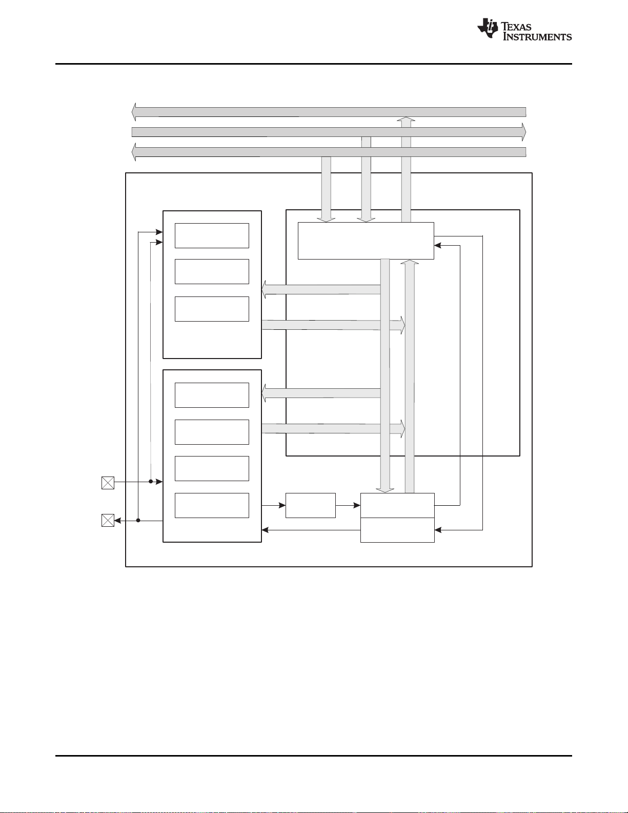
INTERFACE
CHECKSUM
CALCULATOR
TXRXERROR
DETECTOR(TED)
BIT
MONITOR
IDPARTY
CHECKER
MASK
FILTER
TIMEOUT
CONTROL
COUNTER
SYNCHRONIZER
FSM
COMPARE
ADDRESSBUS
READDATA BUS
WRITEDATA BUS
8RECEIVE
BUFFERS
8TRANSMIT
BUFFERS
LINRX/
SCIRX
LINTX/
SCITX
TMS320F28030, TMS320F28031, TMS320F28032
TMS320F28033, TMS320F28034, TMS320F28035
SPRS584D–APRIL 2009–REVISED JUNE 2010
Figure 4-8 shows the LIN module block diagram.
www.ti.com
Figure 4-8. LIN Block Diagram
64 Peripherals Copyright © 2009–2010, Texas Instruments Incorporated
Product Folder Link(s): TMS320F28030 TMS320F28031 TMS320F28032 TMS320F28033 TMS320F28034
Submit Documentation Feedback
TMS320F28035
Page 65

TMS320F28030, TMS320F28031, TMS320F28032
TMS320F28033, TMS320F28034, TMS320F28035
www.ti.com
SPRS584D–APRIL 2009–REVISED JUNE 2010
4.6 Enhanced Controller Area Network (eCAN) Module
The CAN module (eCAN-A) has the following features:
• Fully compliant with CAN protocol, version 2.0B
• Supports data rates up to 1 Mbps
• Thirty-two mailboxes, each with the following properties:
– Configurable as receive or transmit
– Configurable with standard or extended identifier
– Has a programmable receive mask
– Supports data and remote frame
– Composed of 0 to 8 bytes of data
– Uses a 32-bit time stamp on receive and transmit message
– Protects against reception of new message
– Holds the dynamically programmable priority of transmit message
– Employs a programmable interrupt scheme with two interrupt levels
– Employs a programmable alarm on transmission or reception time-out
• Low-power mode
• Programmable wake-up on bus activity
• Automatic reply to a remote request message
• Automatic retransmission of a frame in case of loss of arbitration or error
• 32-bit local network time counter synchronized by a specific message (communication in conjunction
with mailbox 16)
• Self-test mode
– Operates in a loopback mode receiving its own message. A "dummy" acknowledge is provided,
thereby eliminating the need for another node to provide the acknowledge bit.
NOTE
For a SYSCLKOUT of 60 MHz, the smallest bit rate possible is 9.375 kbps.
The F2803x CAN has passed the conformance test per ISO/DIS 16845. Contact TI for test report and
exceptions.
Copyright © 2009–2010, Texas Instruments Incorporated Peripherals 65
Submit Documentation Feedback
Product Folder Link(s): TMS320F28030 TMS320F28031 TMS320F28032 TMS320F28033 TMS320F28034
TMS320F28035
Page 66

Mailbox RAM
(512 Bytes)
32-Message Mailbox
of 4 x 32-Bit Words
Memory Management
Unit
CPU Interface,
Receive Control Unit,
Timer Management Unit
eCAN Memory
(512 Bytes)
Registers and
Message Objects Control
Message Controller
32 32
eCAN Protocol Kernel
Receive Buffer
Transmit Buffer
Control Buffer
Status Buffer
Enhanced CAN Controller
32
Controls
Address Data
eCAN1INTeCAN0INT
32
SN65HVD23x
3.3-V CAN Transceiver
CAN Bus
TMS320F28030, TMS320F28031, TMS320F28032
TMS320F28033, TMS320F28034, TMS320F28035
SPRS584D–APRIL 2009–REVISED JUNE 2010
www.ti.com
PART NUMBER VREF OTHER T
SN65HVD230 3.3 V Standby Adjustable Yes – –40°C to 85°C
SN65HVD230Q 3.3 V Standby Adjustable Yes – –40°C to 125°C
SN65HVD231 3.3 V Sleep Adjustable Yes – –40°C to 85°C
SN65HVD231Q 3.3 V Sleep Adjustable Yes – –40°C to 125°C
SN65HVD232 3.3 V None None None – –40°C to 85°C
SN65HVD232Q 3.3 V None None None – –40°C to 125°C
SN65HVD233 3.3 V Standby Adjustable None Diagnostic Loopback –40°C to 125°C
SN65HVD234 3.3 V Standby and Sleep Adjustable None – –40°C to 125°C
SN65HVD235 3.3 V Standby Adjustable None Autobaud Loopback –40°C to 125°C
ISO1050 3–5.5 V None None None Built-in Isolation –55°C to 105°C
66 Peripherals Copyright © 2009–2010, Texas Instruments Incorporated
SUPPLY LOW-POWER SLOPE
VOLTAGE MODE CONTROL
Product Folder Link(s): TMS320F28030 TMS320F28031 TMS320F28032 TMS320F28033 TMS320F28034
Figure 4-9. eCAN Block Diagram and Interface Circuit
Table 4-10. 3.3-V eCAN Transceivers
Submit Documentation Feedback
TMS320F28035
Low Prop Delay
Thermal Shutdown
Failsafe Operation
Dominant Time-Out
A
Page 67

Mailbox Enable - CANME
Mailbox Direction - CANMD
Transmission Request Set - CANTRS
Transmission Request Reset - CANTRR
Transmission Acknowledge - CANTA
Abort Acknowledge - CANAA
Received Message Pending - CANRMP
Received Message Lost - CANRML
Remote Frame Pending - CANRFP
Global Acceptance Mask - CANGAM
Master Control - CANMC
Bit-Timing Configuration - CANBTC
Error and Status - CANES
Transmit Error Counter - CANTEC
Receive Error Counter - CANREC
Global Interrupt Flag 0 - CANGIF0
Global Interrupt Mask - CANGIM
Mailbox Interrupt Mask - CANMIM
Mailbox Interrupt Level - CANMIL
Overwrite Protection Control - CANOPC
TX I/O Control - CANTIOC
RX I/O Control - CANRIOC
Time Stamp Counter - CANTSC
Global Interrupt Flag 1 - CANGIF1
Time-Out Control - CANTOC
Time-Out Status - CANTOS
Reserved
eCAN-A Control and Status Registers
Message Identifier - MSGID
61E8h-61E9h
Message Control - MSGCTRL
Message Data Low - MDL
Message Data High - MDH
Message Mailbox (16 Bytes)
Control and Status Registers
6000h
603Fh
Local Acceptance Masks (LAM)
(32 x 32-Bit RAM)
6040h
607Fh
6080h
60BFh
60C0h
60FFh
eCAN-A Memory (512 Bytes)
Message Object Time Stamps (MOTS)
(32 x 32-Bit RAM)
Message Object Time-Out (MOTO)
(32 x 32-Bit RAM)
Mailbox 06100h-6107h
Mailbox 1
6108h-610Fh
Mailbox 2
6110h-6117h
Mailbox 3
6118h-611Fh
eCAN-A Memory RAM (512 Bytes)
Mailbox 4
6120h-6127h
Mailbox 28
61E0h-61E7h
Mailbox 2961E8h-61EFh
Mailbox 3061F0h-61F7h
Mailbox 31
61F8h-61FFh
61EAh-61EBh
61ECh-61EDh
61EEh-61EFh
TMS320F28030, TMS320F28031, TMS320F28032
TMS320F28033, TMS320F28034, TMS320F28035
www.ti.com
If the eCAN module is not used in an application, the RAM available (LAM, MOTS, MOTO,
and mailbox RAM) can be used as general-purpose RAM. The CAN module clock should be
enabled for this.
Figure 4-10. eCAN-A Memory Map
NOTE
SPRS584D–APRIL 2009–REVISED JUNE 2010
Copyright © 2009–2010, Texas Instruments Incorporated Peripherals 67
Product Folder Link(s): TMS320F28030 TMS320F28031 TMS320F28032 TMS320F28033 TMS320F28034
Submit Documentation Feedback
TMS320F28035
Page 68

TMS320F28030, TMS320F28031, TMS320F28032
TMS320F28033, TMS320F28034, TMS320F28035
SPRS584D–APRIL 2009–REVISED JUNE 2010
The CAN registers listed in Table 4-11 are used by the CPU to configure and control the CAN controller
and the message objects. eCAN control registers only support 32-bit read/write operations. Mailbox RAM
can be accessed as 16 bits or 32 bits. 32-bit accesses are aligned to an even boundary.
Table 4-11. CAN Register Map
REGISTER NAME SIZE (x32) DESCRIPTION
CANME 0x6000 1 Mailbox enable
CANMD 0x6002 1 Mailbox direction
CANTRS 0x6004 1 Transmit request set
CANTRR 0x6006 1 Transmit request reset
CANTA 0x6008 1 Transmission acknowledge
CANAA 0x600A 1 Abort acknowledge
CANRMP 0x600C 1 Receive message pending
CANRML 0x600E 1 Receive message lost
CANRFP 0x6010 1 Remote frame pending
CANGAM 0x6012 1 Global acceptance mask
CANMC 0x6014 1 Master control
CANBTC 0x6016 1 Bit-timing configuration
CANES 0x6018 1 Error and status
CANTEC 0x601A 1 Transmit error counter
CANREC 0x601C 1 Receive error counter
CANGIF0 0x601E 1 Global interrupt flag 0
CANGIM 0x6020 1 Global interrupt mask
CANGIF1 0x6022 1 Global interrupt flag 1
CANMIM 0x6024 1 Mailbox interrupt mask
CANMIL 0x6026 1 Mailbox interrupt level
CANOPC 0x6028 1 Overwrite protection control
CANTIOC 0x602A 1 TX I/O control
CANRIOC 0x602C 1 RX I/O control
CANTSC 0x602E 1 Time stamp counter (Reserved in SCC mode)
CANTOC 0x6030 1 Time-out control (Reserved in SCC mode)
CANTOS 0x6032 1 Time-out status (Reserved in SCC mode)
(1) These registers are mapped to Peripheral Frame 1.
eCAN-A
ADDRESS
(1)
www.ti.com
68 Peripherals Copyright © 2009–2010, Texas Instruments Incorporated
Submit Documentation Feedback
Product Folder Link(s): TMS320F28030 TMS320F28031 TMS320F28032 TMS320F28033 TMS320F28034
TMS320F28035
Page 69

TMS320F28030, TMS320F28031, TMS320F28032
TMS320F28033, TMS320F28034, TMS320F28035
www.ti.com
SPRS584D–APRIL 2009–REVISED JUNE 2010
4.7 Inter-Integrated Circuit (I2C)
The device contains one I2C Serial Port. Figure 4-11 shows how the I2C peripheral module interfaces
within the device.
The I2C module has the following features:
• Compliance with the Philips Semiconductors I2C-bus specification (version 2.1):
– Support for 1-bit to 8-bit format transfers
– 7-bit and 10-bit addressing modes
– General call
– START byte mode
– Support for multiple master-transmitters and slave-receivers
– Support for multiple slave-transmitters and master-receivers
– Combined master transmit/receive and receive/transmit mode
– Data transfer rate of from 10 kbps up to 400 kbps (I2C Fast-mode rate)
• One 4-word receive FIFO and one 4-word transmit FIFO
• One interrupt that can be used by the CPU. This interrupt can be generated as a result of one of the
following conditions:
– Transmit-data ready
– Receive-data ready
– Register-access ready
– No-acknowledgment received
– Arbitration lost
– Stop condition detected
– Addressed as slave
• An additional interrupt that can be used by the CPU when in FIFO mode
• Module enable/disable capability
• Free data format mode
Copyright © 2009–2010, Texas Instruments Incorporated Peripherals 69
Submit Documentation Feedback
Product Folder Link(s): TMS320F28030 TMS320F28031 TMS320F28032 TMS320F28033 TMS320F28034
TMS320F28035
Page 70

I2CXSR
I2CDXR
I2CRSR
I2CDRR
Clock
Synchronizer
Prescaler
Noise Filters
Arbitrator
I2C INT
Peripheral Bus
Interrupt to
CPU/PIE
SDA
SCL
Control/Status
Registers
CPU
I2C Module
TX FIFO
RX FIFO
FIFO Interrupt to
CPU/PIE
TMS320F28030, TMS320F28031, TMS320F28032
TMS320F28033, TMS320F28034, TMS320F28035
SPRS584D–APRIL 2009–REVISED JUNE 2010
www.ti.com
A. The I2C registers are accessed at the SYSCLKOUT rate. The internal timing and signal waveforms of the I2C port are
also at the SYSCLKOUT rate.
B. The clock enable bit (I2CAENCLK) in the PCLKCRO register turns off the clock to the I2C port for low power
operation. Upon reset, I2CAENCLK is clear, which indicates the peripheral internal clocks are off.
Figure 4-11. I2C Peripheral Module Interfaces
The registers in Table 4-12 configure and control the I2C port operation.
Table 4-12. I2C-A Registers
EALLOW
PROTECTED
NAME ADDRESS DESCRIPTION
I2COAR 0x7900 No I2C own address register
I2CIER 0x7901 No I2C interrupt enable register
I2CSTR 0x7902 No I2C status register
I2CCLKL 0x7903 No I2C clock low-time divider register
I2CCLKH 0x7904 No I2C clock high-time divider register
I2CCNT 0x7905 No I2C data count register
I2CDRR 0x7906 No I2C data receive register
I2CSAR 0x7907 No I2C slave address register
I2CDXR 0x7908 No I2C data transmit register
I2CMDR 0x7909 No I2C mode register
I2CISRC 0x790A No I2C interrupt source register
I2CPSC 0x790C No I2C prescaler register
I2CFFTX 0x7920 No I2C FIFO transmit register
I2CFFRX 0x7921 No I2C FIFO receive register
I2CRSR – No I2C receive shift register (not accessible to the CPU)
I2CXSR – No I2C transmit shift register (not accessible to the CPU)
70 Peripherals Copyright © 2009–2010, Texas Instruments Incorporated
Product Folder Link(s): TMS320F28030 TMS320F28031 TMS320F28032 TMS320F28033 TMS320F28034
Submit Documentation Feedback
TMS320F28035
Page 71

TMS320F28030, TMS320F28031, TMS320F28032
TMS320F28033, TMS320F28034, TMS320F28035
www.ti.com
SPRS584D–APRIL 2009–REVISED JUNE 2010
4.8 Enhanced PWM Modules (ePWM1/2/3/4/5/6/7)
The devices contain up to seven enhanced PWM Modules (ePWM). Figure 4-12 shows a block diagram of
multiple ePWM modules. Figure 4-13 shows the signal interconnections with the ePWM. See the
TMS320x2802x, 2803x Piccolo Enhanced Pulse Width Modulator (ePWM) Module Reference Guide
(literature number SPRUGE9) for more details.
Table 4-13 and Table 4-14 show the complete ePWM register set per module.
Copyright © 2009–2010, Texas Instruments Incorporated Peripherals 71
Submit Documentation Feedback
Product Folder Link(s): TMS320F28030 TMS320F28031 TMS320F28032 TMS320F28033 TMS320F28034
TMS320F28035
Page 72

EPWM1TZINT
PIE
EPWM1INT
EPWM2TZINT
EPWM2INT
EPWMxTZINT
EPWMxINT
COMPOUT1
COMPOUT2
COMP
SOCA1
ADC
SOCB1
SOCA2
SOCB2
SOCAx
SOCBx
EPWM1SYNCI
EPWM2SYNCI
EPWM1SYNCO
EPWM2SYNCO
EPWM1
Module
EPWM2
Module
EPWMxSYNCI
EPWMx
Module
TZ6
TZ6
TZ1 TZ3to
TZ5
CLOCKFAIL
TZ4
EQEP1ERR
(A)
EMUSTOP
TZ5
CLOCKFAIL
TZ4
EQEP1ERR
(A)
EMUSTOP
EPWM1ENCLK
TBCLKSYNC
EPWM2ENCLK
TBCLKSYNC
TZ5
TZ6
EPWMxENCLK
TBCLKSYNC
CLOCKFAIL
TZ4
EQEP1ERR
(A)
EMUSTOP
EPWM1B
C28xCPU
SystemControl
eQEP1
TZ1 TZ3to
TZ1 TZ3to
EPWM1SYNCO
EPWM2B
eCAPI
EPWMxB
EQEP1ERR
H
R
P
W
M
EPWMxA
EPWM2A
EPWM1A
G
P
I
O
M
U
X
ADCSOCBO
ADCSOCAO
PeripheralBus
PulseStretch
(32SYSCLKOUTCycles, Active-LowOutput)
SOCA1
SOCA2
SPCAx
PulseStretch
(32SYSCLKOUTCycles, Active-LowOutput)
SOCB1
SOCB2
SPCBx
EPWMSYNCI
TMS320F28030, TMS320F28031, TMS320F28032
TMS320F28033, TMS320F28034, TMS320F28035
SPRS584D–APRIL 2009–REVISED JUNE 2010
www.ti.com
A. This signal exists only on devices with an eQEP1 module.
Figure 4-12. ePWM
72 Peripherals Copyright © 2009–2010, Texas Instruments Incorporated
Product Folder Link(s): TMS320F28030 TMS320F28031 TMS320F28032 TMS320F28033 TMS320F28034
Submit Documentation Feedback
TMS320F28035
Page 73

TMS320F28030, TMS320F28031, TMS320F28032
TMS320F28033, TMS320F28034, TMS320F28035
www.ti.com
SPRS584D–APRIL 2009–REVISED JUNE 2010
Table 4-13. ePWM1–ePWM4 Control and Status Registers
NAME ePWM1 ePWM2 ePWM3 ePWM4 DESCRIPTION
TBCTL 0x6800 0x6840 0x6880 0x68C0 1 / 0 Time Base Control Register
TBSTS 0x6801 0x6841 0x6881 0x68C1 1 / 0 Time Base Status Register
TBPHSHR 0x6802 0x6842 0x6882 0x68C2 1 / 0 Time Base Phase HRPWM Register
TBPHS 0x6803 0x6843 0x6883 0x68C3 1 / 0 Time Base Phase Register
TBCTR 0x6804 0x6844 0x6884 0x68C4 1 / 0 Time Base Counter Register
TBPRD 0x6805 0x6845 0x6885 0x68C5 1 / 1 Time Base Period Register Set
TBPRDHR 0x6806 0x6846 0x6886 0x68C6 1 / 1 Time Base Period High Resolution Register
CMPCTL 0x6807 0x6847 0x6887 0x68C7 1 / 0 Counter Compare Control Register
CMPAHR 0x6808 0x6848 0x6888 0x68C8 1 / 1 Time Base Compare A HRPWM Register
CMPA 0x6809 0x6849 0x6889 0x68C9 1 / 1 Counter Compare A Register Set
CMPB 0x680A 0x684A 0x688A 0x68CA 1 / 1 Counter Compare B Register Set
AQCTLA 0x680B 0x684B 0x688B 0x68CB 1 / 0 Action Qualifier Control Register For Output A
AQCTLB 0x680C 0x684C 0x688C 0x68CC 1 / 0 Action Qualifier Control Register For Output B
AQSFRC 0x680D 0x684D 0x688D 0x68CD 1 / 0 Action Qualifier Software Force Register
AQCSFRC 0x680E 0x684E 0x688E 0x68CE 1 / 1 Action Qualifier Continuous S/W Force Register Set
DBCTL 0x680F 0x684F 0x688F 0x68CF 1 / 1 Dead-Band Generator Control Register
DBRED 0x6810 0x6850 0x6890 0x68D0 1 / 0 Dead-Band Generator Rising Edge Delay Count Register
DBFED 0x6811 0x6851 0x6891 0x68D1 1 / 0 Dead-Band Generator Falling Edge Delay Count Register
TZSEL 0x6812 0x6852 0x6892 0x68D2 1 / 0 Trip Zone Select Register
TZDCSEL 0x6813 0x6853 0x6893 0x98D3 1 / 0 Trip Zone Digital Compare Register
TZCTL 0x6814 0x6854 0x6894 0x68D4 1 / 0 Trip Zone Control Register
TZEINT 0x6815 0x6855 0x6895 0x68D5 1 / 0 Trip Zone Enable Interrupt Register
TZFLG 0x6816 0x6856 0x6896 0x68D6 1 / 0 Trip Zone Flag Register
TZCLR 0x6817 0x6857 0x6897 0x68D7 1 / 0 Trip Zone Clear Register
TZFRC 0x6818 0x6858 0x6898 0x68D8 1 / 0 Trip Zone Force Register
ETSEL 0x6819 0x6859 0x6899 0x68D9 1 / 0 Event Trigger Selection Register
ETPS 0x681A 0x685A 0x689A 0x68DA 1 / 0 Event Trigger Prescale Register
ETFLG 0x681B 0x685B 0x689B 0x68DB 1 / 0 Event Trigger Flag Register
ETCLR 0x681C 0x685C 0x689C 0x68DC 1 / 0 Event Trigger Clear Register
ETFRC 0x681D 0x685D 0x689D 0x68DD 1 / 0 Event Trigger Force Register
PCCTL 0x681E 0x685E 0x689E 0x68DE 1 / 0 PWM Chopper Control Register
HRCNFG 0x6820 0x6860 0x68A0 0x68E0 1 / 0 HRPWM Configuration Register
SIZE (x16) /
#SHADOW
(1)
(1)
(1)
(1)
(1)
(1)
(1)
(1)
(1) Registers that are EALLOW protected.
Copyright © 2009–2010, Texas Instruments Incorporated Peripherals 73
Submit Documentation Feedback
Product Folder Link(s): TMS320F28030 TMS320F28031 TMS320F28032 TMS320F28033 TMS320F28034
TMS320F28035
Page 74

TMS320F28030, TMS320F28031, TMS320F28032
TMS320F28033, TMS320F28034, TMS320F28035
SPRS584D–APRIL 2009–REVISED JUNE 2010
Table 4-13. ePWM1–ePWM4 Control and Status Registers (continued)
NAME ePWM1 ePWM2 ePWM3 ePWM4 DESCRIPTION
HRPWR 0x6821 - - - 1 / 0 HRPWM Power Register
HRMSTEP 0x6826 - - - 1 / 0 HRPWM MEP Step Register
HRPCTL 0x6828 0x6868 0x68A8 0x68E8 1 / 0 High resolution Period Control Register
TBPRDHRM 0x682A 0x686A 0x68AA 0x68EA 1 / W
TBPRDM 0x682B 0x686B 0x68AB 0x68EB 1 / W
CMPAHRM 0x682C 0x686C 0x68AC 0x68EC 1 / W
CMPAM 0x682D 0x686D 0x68AD 0x68ED 1 / W
DCTRIPSEL 0x6830 0x6870 0x68B0 0x68F0 1 / 0 Digital Compare Trip Select Register
DCACTL 0x6831 0x6871 0x68B1 0x68F1 1 / 0 Digital Compare A Control Register
DCBCTL 0x6832 0x6872 0x68B2 0x68F2 1 / 0 Digital Compare B Control Register
DCFCTL 0x6833 0x6873 0x68B3 0x68F3 1 / 0 Digital Compare Filter Control Register
DCCAPCT 0x6834 0x6874 0x68B4 0x68F4 1 / 0 Digital Compare Capture Control Register
DCFOFFSET 0x6835 0x6875 0x68B5 0x68F5 1 / 1 Digital Compare Filter Offset Register
DCFOFFSETCNT 0x6836 0x6876 0x68B6 0x68F6 1 / 0 Digital Compare Filter Offset Counter Register
DCFWINDOW 0x6837 0x6877 0x68B7 0x68F7 1 / 0 Digital Compare Filter Window Register
DCFWINDOWCNT 0x6838 0x6878 0x68B8 0x68F8 1 / 0 Digital Compare Filter Window Counter Register
DCCAP 0x6839 0x6879 0x68B9 0x68F9 1 / 1 Digital Compare Counter Capture Register
(2) W = Write to shadow register
SIZE (x16) /
#SHADOW
(2)
(2)
(2)
(2)
(1)
Time Base Period HRPWM Register Mirror
Time Base Period Register Mirror
Compare A HRPWM Register Mirror
Compare A Register Mirror
(1)
(1)
(1)
(1)
(1)
www.ti.com
Table 4-14. ePWM5–ePWM7 Control and Status Registers
NAME ePWM5 ePWM6 ePWM7 DESCRIPTION
TBCTL 0x6900 0x6940 0x6980 1 / 0 Time Base Control Register
TBSTS 0x6901 0x6941 0x6981 1 / 0 Time Base Status Register
TBPHSHR 0x6902 0x6942 0x6982 1 / 0 Time Base Phase HRPWM Register
TBPHS 0x6903 0x6943 0x6983 1 / 0 Time Base Phase Register
TBCTR 0x6904 0x6944 0x6984 1 / 0 Time Base Counter Register
TBPRD 0x6905 0x6945 0x6985 1 / 1 Time Base Period Register Set
TBPRDHR 0x6906 0x6946 0x6986 1 / 1 Time Base Period High Resolution Register
CMPCTL 0x6907 0x6947 0x6987 1 / 0 Counter Compare Control Register
CMPAHR 0x6908 0x6948 0x6988 1 / 1 Time Base Compare A HRPWM Register
CMPA 0x6909 0x6949 0x6989 1 / 1 Counter Compare A Register Set
(1) Registers that are EALLOW protected.
74 Peripherals Copyright © 2009–2010, Texas Instruments Incorporated
Submit Documentation Feedback
Product Folder Link(s): TMS320F28030 TMS320F28031 TMS320F28032 TMS320F28033 TMS320F28034
TMS320F28035
SIZE (x16) /
#SHADOW
(1)
Page 75

TMS320F28030, TMS320F28031, TMS320F28032
TMS320F28033, TMS320F28034, TMS320F28035
www.ti.com
SPRS584D–APRIL 2009–REVISED JUNE 2010
Table 4-14. ePWM5–ePWM7 Control and Status Registers (continued)
NAME ePWM5 ePWM6 ePWM7 DESCRIPTION
CMPB 0x690A 0x694A 0x698A 1 / 1 Counter Compare B Register Set
AQCTLA 0x690B 0x694B 0x698B 1 / 0 Action Qualifier Control Register For Output A
AQCTLB 0x690C 0x694C 0x698C 1 / 0 Action Qualifier Control Register For Output B
AQSFRC 0x690D 0x694D 0x698D 1 / 0 Action Qualifier Software Force Register
AQCSFRC 0x690E 0x694E 0x698E 1 / 1 Action Qualifier Continuous S/W Force Register Set
DBCTL 0x690F 0x694F 0x698F 1 / 1 Dead-Band Generator Control Register
DBRED 0x6910 0x6950 0x6990 1 / 0 Dead-Band Generator Rising Edge Delay Count Register
DBFED 0x6911 0x6951 0x6991 1 / 0 Dead-Band Generator Falling Edge Delay Count Register
TZSEL 0x6912 0x6952 0x6992 1 / 0 Trip Zone Select Register
TZDCSEL 0x6913 0x6953 0x6993 1 / 0 Trip Zone Digital Compare Register
TZCTL 0x6914 0x6954 0x6994 1 / 0 Trip Zone Control Register
TZEINT 0x6915 0x6955 0x6995 1 / 0 Trip Zone Enable Interrupt Register
TZFLG 0x6916 0x6956 0x6996 1 / 0 Trip Zone Flag Register
TZCLR 0x6917 0x6957 0x6997 1 / 0 Trip Zone Clear Register
TZFRC 0x6918 0x6958 0x6998 1 / 0 Trip Zone Force Register
ETSEL 0x6919 0x6959 0x6999 1 / 0 Event Trigger Selection Register
ETPS 0x691A 0x695A 0x699A 1 / 0 Event Trigger Prescale Register
ETFLG 0x691B 0x695B 0x699B 1 / 0 Event Trigger Flag Register
ETCLR 0x691C 0x695C 0x699C 1 / 0 Event Trigger Clear Register
ETFRC 0x691D 0x695D 0x699D 1 / 0 Event Trigger Force Register
PCCTL 0x691E 0x695E 0x699E 1 / 0 PWM Chopper Control Register
HRCNFG 0x6920 0x6960 0x69A0 1 / 0 HRPWM Configuration Register
HRPWR - - - 1 / 0 HRPWM Power Register
HRMSTEP - - - 1 / 0 HRPWM MEP Step Register
HRPCTL 0x6928 0x6968 0x69A8 1 / 0 High resolution Period Control Register
TBPRDHRM 0x692A 0x696A 0x69AA 1 / W
TBPRDM 0x692B 0x696B 0x69AB 1 / W
CMPAHRM 0x692C 0x696C 0x69AC 1 / W
CMPAM 0x692D 0x696D 0x69AD 1 / W
DCTRIPSEL 0x6930 0x6970 0x69B0 1 / 0 Digital Compare Trip Select Register
DCACTL 0x6931 0x6971 0x69B1 1 / 0 Digital Compare A Control Register
SIZE (x16) /
#SHADOW
(3)
(3)
(3)
(3)
(1)
(1)
(1)
(1)
(2)
(2)
(2)
(2)
Time Base Period HRPWM Register Mirror
Time Base Period Register Mirror
Compare A HRPWM Register Mirror
Compare A Register Mirror
(2)
(2)
(2) Registers that are EALLOW protected.
(3) W = Write to shadow register
Copyright © 2009–2010, Texas Instruments Incorporated Peripherals 75
Submit Documentation Feedback
Product Folder Link(s): TMS320F28030 TMS320F28031 TMS320F28032 TMS320F28033 TMS320F28034
TMS320F28035
Page 76

TMS320F28030, TMS320F28031, TMS320F28032
TMS320F28033, TMS320F28034, TMS320F28035
SPRS584D–APRIL 2009–REVISED JUNE 2010
Table 4-14. ePWM5–ePWM7 Control and Status Registers (continued)
NAME ePWM5 ePWM6 ePWM7 DESCRIPTION
DCBCTL 0x6932 0x6972 0x69B2 1 / 0 Digital Compare B Control Register
DCFCTL 0x6933 0x6973 0x69B3 1 / 0 Digital Compare Filter Control Register
DCCAPCT 0x6934 0x6974 0x69B4 1 / 0 Digital Compare Capture Control Register
DCFOFFSET 0x6935 0x6975 0x69B5 1 / 1 Digital Compare Filter Offset Register
DCFOFFSETCNT 0x6936 0x6976 0x69B6 1 / 0 Digital Compare Filter Offset Counter Register
DCFWINDOW 0x6937 0x6977 0x69B7 1 / 0 Digital Compare Filter Window Register
DCFWINDOWCNT 0x6938 0x6978 0x69B8 1 / 0 Digital Compare Filter Window Counter Register
DCCAP 0x6939 0x6979 0x69B9 1 / 1 Digital Compare Counter Capture Register
SIZE (x16) /
#SHADOW
(2)
(2)
(2)
www.ti.com
76 Peripherals Copyright © 2009–2010, Texas Instruments Incorporated
Submit Documentation Feedback
Product Folder Link(s): TMS320F28030 TMS320F28031 TMS320F28032 TMS320F28033 TMS320F28034
TMS320F28035
Page 77

TBPRD Shadow (24)
TBPRD Active (24)
Counter
Up/Down
(16 Bit)
TCBNT
Active (16)
TBCTL[PHSEN]
CTR=PRD
16
Phase
Control
8
CTR=ZERO
CTR_Dir
TBPHSHR (8)
TBPRDHR (8)
8
CTR=ZERO
CTR=CMPB
Disabled
TBCTL[SYNCOSEL]
EPWMxSYNCO
Time-Base (TB)
TBPHS Active (24)
Sync
In/Out
Select
Mux
CTR=PRD
CTR=ZERO
CTR=CMPA
CTR=CMPB
CTR_Dir
DCAEVT1.soc
(A)
DCBEVT1.soc
(A)
Event
Trigger
and
Interrupt
(ET)
EPWMxINT
EPWMxSOCA
EPWMxSOCB
EPWMxSOCA
EPWMxSOCB
ADC
Action
Qualifier
(AQ)
EPWMA
Dead
Band
(DB)
EPWMB
PWM
Chopper
(PC)
Trip
Zone
(TZ)
EPWMxA
EPWMxB
CTR=ZERO
EPWMxTZINT
TZ1 TZ3to
EMUSTOP
CLOCKFAIL
EQEP1ERR
(B)
DCAEVT1.force
(A)
DCAEVT2.force
(A)
DCBEVT1.force
(A)
DCBEVT2.force
(A)
CTR=CMPA
16
CMPAHR (8)
CTR=CMPB
16
CMPB Active (16)
CMPB Shadow (16)
HiRes PWM (HRPWM)
CTR=PRD or ZERO
DCAEVT1.inter
DCBEVT1.inter
DCAEVT2.inter
DCBEVT2.inter
EPWMxSYNCI
TBCTL[SWFSYNC]
(Software Forced
Sync)
DCAEVT1.sync
DCBEVT1.sync
CMPAActive (24)
CMPA Shadow (24)
TMS320F28030, TMS320F28031, TMS320F28032
TMS320F28033, TMS320F28034, TMS320F28035
www.ti.com
SPRS584D–APRIL 2009–REVISED JUNE 2010
A. These events are generated by the Type 1 ePWM digital compare (DC) submodule based on the levels of
the COMPxOUT and TZ signals.
B. This signal exists only on devices with an eQEP1 module.
Figure 4-13. ePWM Sub-Modules Showing Critical Internal Signal Interconnections
Copyright © 2009–2010, Texas Instruments Incorporated Peripherals 77
Product Folder Link(s): TMS320F28030 TMS320F28031 TMS320F28032 TMS320F28033 TMS320F28034
Submit Documentation Feedback
TMS320F28035
Page 78

TMS320F28030, TMS320F28031, TMS320F28032
TMS320F28033, TMS320F28034, TMS320F28035
SPRS584D–APRIL 2009–REVISED JUNE 2010
4.9 High-Resolution PWM (HRPWM)
This module combines multiple delay lines in a single module and a simplified calibration system by using
a dedicated calibration delay line. For each ePWM module there is one HR delay line.
The HRPWM module offers PWM resolution (time granularity) that is significantly better than what can be
achieved using conventionally derived digital PWM methods. The key points for the HRPWM module are:
• Significantly extends the time resolution capabilities of conventionally derived digital PWM
• This capability can be utilized in both single edge (duty cycle and phase-shift control) as well as dual
edge control for frequency/period modulation.
• Finer time granularity control or edge positioning is controlled via extensions to the Compare A and
Phase registers of the ePWM module.
• HRPWM capabilities, when available on a particular device, are offered only on the A signal path of an
ePWM module (i.e., on the EPWMxA output). EPWMxB output has conventional PWM capabilities.
NOTE
The minimum SYSCLKOUT frequency allowed for HRPWM is 60 MHz.
NOTE
When dual-edge high-resolution is enabled (high-resolution period mode), the PWMxB output
is not available for use.
www.ti.com
78 Peripherals Copyright © 2009–2010, Texas Instruments Incorporated
Submit Documentation Feedback
Product Folder Link(s): TMS320F28030 TMS320F28031 TMS320F28032 TMS320F28033 TMS320F28034
TMS320F28035
Page 79

TSCTR
(counter−32bit)
RST
CAP1
(APRDactive)
LD
CAP2
(ACMPactive)
LD
CAP3
(APRDshadow)
LD
CAP4
(ACMPshadow)
LD
Continuous/
Oneshot
CaptureControl
LD1
LD2
LD3
LD4
32
32
PRD[0−31]
CMP[0−31]
CTR[0−31]
eCAPx
Interrupt
Trigger
and
Flag
control
toPIE
CTR=CMP
32
32
32
32
32
ACMP
shadow
Event
Pre-scale
CTRPHS
(phaseregister−32bit)
SYNCOut
SYNCIn
Event
qualifier
Polarity
select
Polarity
select
Polarity
select
Polarity
select
CTR=PRD
CTR_OVF
4
PWM
compare
logic
CTR[0−31]
PRD[0−31]
CMP[0−31]
CTR=CMP
CTR=PRD
CTR_OVF
OVF
APWMmode
Delta−mode
SYNC
4
Captureevents
CEVT[1:4]
APRD
shadow
32
32
MODESELECT
TMS320F28030, TMS320F28031, TMS320F28032
TMS320F28033, TMS320F28034, TMS320F28035
www.ti.com
SPRS584D–APRIL 2009–REVISED JUNE 2010
4.10 Enhanced Capture Module (eCAP1)
The device contains an enhanced capture (eCAP) module. Figure 4-14 shows a functional block diagram
of a module.
Figure 4-14. eCAP Functional Block Diagram
The eCAP module is clocked at the SYSCLKOUT rate.
The clock enable bits (ECAP1 ENCLK) in the PCLKCR1 register turn off the eCAP module individually (for
low power operation). Upon reset, ECAP1ENCLK is set to low, indicating that the peripheral clock is off.
Copyright © 2009–2010, Texas Instruments Incorporated Peripherals 79
Product Folder Link(s): TMS320F28030 TMS320F28031 TMS320F28032 TMS320F28033 TMS320F28034
Submit Documentation Feedback
TMS320F28035
Page 80

TMS320F28030, TMS320F28031, TMS320F28032
TMS320F28033, TMS320F28034, TMS320F28035
SPRS584D–APRIL 2009–REVISED JUNE 2010
Table 4-15. eCAP Control and Status Registers
NAME eCAP1 SIZE (x16) EALLOW PROTECTED DESCRIPTION
TSCTR 0x6A00 2 Time-Stamp Counter
CTRPHS 0x6A02 2 Counter Phase Offset Value Register
CAP1 0x6A04 2 Capture 1 Register
CAP2 0x6A06 2 Capture 2 Register
CAP3 0x6A08 2 Capture 3 Register
CAP4 0x6A0A 2 Capture 4 Register
Reserved 0x6A0C – 0x6A12 8 Reserved
ECCTL1 0x6A14 1 Capture Control Register 1
ECCTL2 0x6A15 1 Capture Control Register 2
ECEINT 0x6A16 1 Capture Interrupt Enable Register
ECFLG 0x6A17 1 Capture Interrupt Flag Register
ECCLR 0x6A18 1 Capture Interrupt Clear Register
ECFRC 0x6A19 1 Capture Interrupt Force Register
Reserved 0x6A1A – 0x6A1F 6 Reserved
www.ti.com
80 Peripherals Copyright © 2009–2010, Texas Instruments Incorporated
Submit Documentation Feedback
Product Folder Link(s): TMS320F28030 TMS320F28031 TMS320F28032 TMS320F28033 TMS320F28034
TMS320F28035
Page 81

TMS320F28030, TMS320F28031, TMS320F28032
TMS320F28033, TMS320F28034, TMS320F28035
www.ti.com
SPRS584D–APRIL 2009–REVISED JUNE 2010
4.11 Enhanced Quadrature Encoder Pulse (eQEP)
The device contains one enhanced quadrature encoder pulse (eQEP) module.
Table 4-16. eQEP Control and Status Registers
NAME SIZE(x16)/ REGISTER DESCRIPTION
QPOSCNT 0x6B00 2/0 eQEP Position Counter
QPOSINIT 0x6B02 2/0 eQEP Initialization Position Count
QPOSMAX 0x6B04 2/0 eQEP Maximum Position Count
QPOSCMP 0x6B06 2/1 eQEP Position-compare
QPOSILAT 0x6B08 2/0 eQEP Index Position Latch
QPOSSLAT 0x6B0A 2/0 eQEP Strobe Position Latch
QPOSLAT 0x6B0C 2/0 eQEP Position Latch
QUTMR 0x6B0E 2/0 eQEP Unit Timer
QUPRD 0x6B10 2/0 eQEP Unit Period Register
QWDTMR 0x6B12 1/0 eQEP Watchdog Timer
QWDPRD 0x6B13 1/0 eQEP Watchdog Period Register
QDECCTL 0x6B14 1/0 eQEP Decoder Control Register
QEPCTL 0x6B15 1/0 eQEP Control Register
QCAPCTL 0x6B16 1/0 eQEP Capture Control Register
QPOSCTL 0x6B17 1/0 eQEP Position-compare Control Register
QEINT 0x6B18 1/0 eQEP Interrupt Enable Register
QFLG 0x6B19 1/0 eQEP Interrupt Flag Register
QCLR 0x6B1A 1/0 eQEP Interrupt Clear Register
QFRC 0x6B1B 1/0 eQEP Interrupt Force Register
QEPSTS 0x6B1C 1/0 eQEP Status Register
QCTMR 0x6B1D 1/0 eQEP Capture Timer
QCPRD 0x6B1E 1/0 eQEP Capture Period Register
QCTMRLAT 0x6B1F 1/0 eQEP Capture Timer Latch
QCPRDLAT 0x6B20 1/0 eQEP Capture Period Latch
Reserved 0x6B21 – 31/0
eQEP1
ADDRESS
0x6B3F
eQEP1
#SHADOW
Copyright © 2009–2010, Texas Instruments Incorporated Peripherals 81
Submit Documentation Feedback
Product Folder Link(s): TMS320F28030 TMS320F28031 TMS320F28032 TMS320F28033 TMS320F28034
TMS320F28035
Page 82

QWDTMR
QWDPRD
16
QWDOG
UTIME
QUPRD
QUTMR
32
UTOUT
WDTOUT
Quadrature
Capture
Unit
(QCAP)
QCPRDLAT
QCTMRLAT
16
QFLG
QEPSTS
QEPCTL
Registers
Used by
Multiple Units
QCLK
QDIR
QI
QS
PHE
PCSOUT
Quadrature
Decoder
(QDU)
QDECCTL
16
Position Counter/
Control Unit
(PCCU)
QPOSLAT
QPOSSLAT
16
QPOSILAT
EQEPxAIN
EQEPxBIN
EQEPxIIN
EQEPxIOUT
EQEPxIOE
EQEPxSIN
EQEPxSOUT
EQEPxSOE
GPIO
MUX
EQEPxA/XCLK
EQEPxB/XDIR
EQEPxS
EQEPxI
QPOSCMP
QEINT
QFRC
32
QCLR
QPOSCTL
1632
QPOSCNT
QPOSMAX
QPOSINIT
PIE
EQEPxINT
Enhanced QEP (eQEP) Peripheral
System Control
Registers
QCTMR
QCPRD
1616
QCAPCTL
EQEPxENCLK
SYSCLKOUT
To CPU
Data Bus
TMS320F28030, TMS320F28031, TMS320F28032
TMS320F28033, TMS320F28034, TMS320F28035
SPRS584D–APRIL 2009–REVISED JUNE 2010
Figure 4-15 shows the eQEP functional block diagram.
www.ti.com
Figure 4-15. eQEP Functional Block Diagram
82 Peripherals Copyright © 2009–2010, Texas Instruments Incorporated
Product Folder Link(s): TMS320F28030 TMS320F28031 TMS320F28032 TMS320F28033 TMS320F28034
Submit Documentation Feedback
TMS320F28035
Page 83

TRST
1
0
C28x
Core
TCK/GPIO38
TCK
XCLKIN
GPIO38_in
GPIO38_out
TDO
GPIO37_out
TDO/GPIO37
GPIO37_in
1
0
TMS
TMS/GPIO36
GPIO36_out
GPIO36_in
1
1
0
TDI
TDI/GPIO35
GPIO35_out
GPIO35_in
1
TRST
TRST
=0:JTAGDisabled(GPIOMode)
=1:JTAGMode
TRST
TMS320F28030, TMS320F28031, TMS320F28032
TMS320F28033, TMS320F28034, TMS320F28035
www.ti.com
SPRS584D–APRIL 2009–REVISED JUNE 2010
4.12 JTAG Port
On the 2803x device, the JTAG port is reduced to 5 pins (TRST, TCK, TDI, TMS, TDO). TCK, TDI, TMS
and TDO pins are also GPIO pins. The TRST signal selects either JTAG or GPIO operating mode for the
pins in Figure 4-16. During emulation/debug, the GPIO function of these pins are not available. If the
GPIO38/TCK/XCLKIN pin is used to provide an external clock, an alternate clock source should be used
to clock the device during emulation/debug since this pin will be needed for the TCK function.
NOTE
In 2803x devices, the JTAG pins may also be used as GPIO pins. Care should be taken in
the board design to ensure that the circuitry connected to these pins do not affect the
emulation capabilities of the JTAG pin function. Any circuitry connected to these pins should
not prevent the emulator from driving (or being driven by) the JTAG pins for successful
debug.
Copyright © 2009–2010, Texas Instruments Incorporated Peripherals 83
Figure 4-16. JTAG/GPIO Multiplexing
Submit Documentation Feedback
Product Folder Link(s): TMS320F28030 TMS320F28031 TMS320F28032 TMS320F28033 TMS320F28034
TMS320F28035
Page 84

TMS320F28030, TMS320F28031, TMS320F28032
TMS320F28033, TMS320F28034, TMS320F28035
SPRS584D–APRIL 2009–REVISED JUNE 2010
4.13 GPIO MUX
The GPIO MUX can multiplex up to three independent peripheral signals on a single GPIO pin in addition
to providing individual pin bit-banging I/O capability.
The device supports 45 GPIO pins. The GPIO control and data registers are mapped to Peripheral
Frame 1 to enable 32-bit operations on the registers (along with 16-bit operations). Table 4-17 shows the
GPIO register mapping.
Table 4-17. GPIO Registers
NAME ADDRESS SIZE (x16) DESCRIPTION
GPIO CONTROL REGISTERS (EALLOW PROTECTED)
GPACTRL 0x6F80 2 GPIO A Control Register (GPIO0 to 31)
GPAQSEL1 0x6F82 2 GPIO A Qualifier Select 1 Register (GPIO0 to 15)
GPAQSEL2 0x6F84 2 GPIO A Qualifier Select 2 Register (GPIO16 to 31)
GPAMUX1 0x6F86 2 GPIO A MUX 1 Register (GPIO0 to 15)
GPAMUX2 0x6F88 2 GPIO A MUX 2 Register (GPIO16 to 31)
GPADIR 0x6F8A 2 GPIO A Direction Register (GPIO0 to 31)
GPAPUD 0x6F8C 2 GPIO A Pull Up Disable Register (GPIO0 to 31)
GPBCTRL 0x6F90 2 GPIO B Control Register (GPIO32 to 44)
GPBQSEL1 0x6F92 2 GPIO B Qualifier Select 1 Register (GPIO32 to 44)
GPBMUX1 0x6F96 2 GPIO B MUX 1 Register (GPIO32 to 44)
GPBDIR 0x6F9A 2 GPIO B Direction Register (GPIO32 to 44)
GPBPUD 0x6F9C 2 GPIO B Pull Up Disable Register (GPIO32 to 44)
AIOMUX1 0x6FB6 2 Analog, I/O mux 1 register (AIO0 to AIO15)
AIODIR 0x6FBA 2 Analog, I/O Direction Register (AIO0 to AIO15)
GPIO DATA REGISTERS (NOT EALLOW PROTECTED)
GPADAT 0x6FC0 2 GPIO A Data Register (GPIO0 to 31)
GPASET 0x6FC2 2 GPIO A Data Set Register (GPIO0 to 31)
GPACLEAR 0x6FC4 2 GPIO A Data Clear Register (GPIO0 to 31)
GPATOGGLE 0x6FC6 2 GPIO A Data Toggle Register (GPIO0 to 31)
GPBDAT 0x6FC8 2 GPIO B Data Register (GPIO32 to 44)
GPBSET 0x6FCA 2 GPIO B Data Set Register (GPIO32 to 44)
GPBCLEAR 0x6FCC 2 GPIO B Data Clear Register (GPIO32 to 44)
GPBTOGGLE 0x6FCE 2 GPIO B Data Toggle Register (GPIO32 to 44)
AIODAT 0x6FD8 2 Analog I/O Data Register (AIO0 to AIO15)
AIOSET 0x6FDA 2 Analog I/O Data Set Register (AIO0 to AIO15)
AIOCLEAR 0x6FDC 2 Analog I/O Data Clear Register (AIO0 to AIO15)
AIOTOGGLE 0x6FDE 2 Analog I/O Data Toggle Register (AIO0 to AIO15)
GPIO INTERRUPT AND LOW POWER MODES SELECT REGISTERS (EALLOW PROTECTED)
GPIOXINT1SEL 0x6FE0 1 XINT1 GPIO Input Select Register (GPIO0 to 31)
GPIOXINT2SEL 0x6FE1 1 XINT2 GPIO Input Select Register (GPIO0 to 31)
GPIOXINT3SEL 0x6FE2 1 XINT3 GPIO Input Select Register (GPIO0 to 31)
GPIOLPMSEL 0x6FE8 2 LPM GPIO Select Register (GPIO0 to 31)
www.ti.com
NOTE
There is a two-SYSCLKOUT cycle delay from when the write to the GPxMUXn/AIOMUXn
and GPxQSELn registers occurs to when the action is valid.
84 Peripherals Copyright © 2009–2010, Texas Instruments Incorporated
Submit Documentation Feedback
Product Folder Link(s): TMS320F28030 TMS320F28031 TMS320F28032 TMS320F28033 TMS320F28034
TMS320F28035
Page 85

TMS320F28030, TMS320F28031, TMS320F28032
TMS320F28033, TMS320F28034, TMS320F28035
www.ti.com
GPAMUX1 REGISTER
BITS
(1) (2)
DEFAULT AT RESET
PRIMARY I/O
FUNCTION
Table 4-18. GPIOA MUX
PERIPHERAL PERIPHERAL PERIPHERAL
SELECTION 1 SELECTION 2 SELECTION 3
(GPAMUX1 BITS = 00) (GPAMUX1 BITS = 01) (GPAMUX1 BITS = 10) (GPAMUX1 BITS = 11)
SPRS584D–APRIL 2009–REVISED JUNE 2010
1-0 GPIO0 EPWM1A (O) Reserved Reserved
3-2 GPIO1 EPWM1B (O) Reserved COMP1OUT (O)
5-4 GPIO2 EPWM2A (O) Reserved Reserved
7-6 GPIO3 EPWM2B (O) SPISOMIA (I/O) COMP2OUT (O)
9-8 GPIO4 EPWM3A (O) Reserved Reserved
11-10 GPIO5 EPWM3B (O) SPISIMOA (I/O) ECAP1 (I/O)
13-12 GPIO6 EPWM4A (O) EPWMSYNCI (I) EPWMSYNCO (O)
15-14 GPIO7 EPWM4B (O) SCIRXDA (I) Reserved
17-16 GPIO8 EPWM5A (O) Reserved ADCSOCAO (O)
19-18 GPIO9 EPWM5B (O) LINTXA (O) Reserved
21-20 GPIO10 EPWM6A (O) Reserved ADCSOCBO (O)
23-22 GPIO11 EPWM6B (O) LINRXA (I) Reserved
25-24 GPIO12 TZ1 (I) SCITXDA (O) SPISIMOB (I/O)
27-26 GPIO13
29-28 GPIO14
31-30 GPIO15
GPAMUX2 REGISTER
BITS
(GPAMUX2 BITS = 00) (GPAMUX2 BITS = 01) (GPAMUX2 BITS = 10) (GPAMUX2 BITS = 11)
(3)
(3)
(3)
TZ2 (I) Reserved SPISOMIB (I/O)
TZ3 (I) LINTXA (O) SPICLKB (I/O)
TZ1 (I) LINRXA (I) SPISTEB (I/O)
1-0 GPIO16 SPISIMOA (I/O) Reserved TZ2 (I)
3-2 GPIO17 SPISOMIA (I/O) Reserved TZ3 (I)
5-4 GPIO18 SPICLKA (I/O) LINTXA (O) XCLKOUT (O)
7-6 GPIO19/XCLKIN SPISTEA (I/O) LINRXA (I) ECAP1 (I/O)
9-8 GPIO20 EQEP1A (I) Reserved COMP1OUT (O)
11-10 GPIO21 EQEP1B (I) Reserved COMP2OUT (O)
13-12 GPIO22 EQEP1S (I/O) Reserved LINTXA (O)
15-14 GPIO23 EQEP1I (I/O) Reserved LINRXA (I)
17-16 GPIO24 ECAP1 (I/O) Reserved SPISIMOB (I/O)
19-18 GPIO25
21-20 GPIO26
23-22 GPIO27
(3)
(3)
(3)
Reserved Reserved SPISOMIB (I/O)
Reserved Reserved SPICLKB (I/O)
Reserved Reserved SPISTEB (I/O)
25-24 GPIO28 SCIRXDA (I) SDAA (I/OD) TZ2 (I)
27-26 GPIO29 SCITXDA (O) SCLA (I/OD) TZ3 (I)
29-28 GPIO30 CANRXA (I) Reserved Reserved
31-30 GPIO31 CANTXA (O) Reserved Reserved
(1) The word reserved means that there is no peripheral assigned to this GPxMUX1/2 register setting. Should it be selected, the state of the
pin will be undefined and the pin may be driven. This selection is a reserved configuration for future expansion.
(2) I = Input, O = Output, OD = Open Drain
(3) These pins are not available in the 64-pin package.
Copyright © 2009–2010, Texas Instruments Incorporated Peripherals 85
Submit Documentation Feedback
Product Folder Link(s): TMS320F28030 TMS320F28031 TMS320F28032 TMS320F28033 TMS320F28034
TMS320F28035
Page 86

TMS320F28030, TMS320F28031, TMS320F28032
TMS320F28033, TMS320F28034, TMS320F28035
SPRS584D–APRIL 2009–REVISED JUNE 2010
Table 4-19. GPIOB MUX
DEFAULT AT RESET PERIPHERAL PERIPHERAL PERIPHERAL
PRIMARY I/O FUNCTION SELECTION 1 SELECTION 2 SELECTION 3
GPBMUX1 REGISTER
BITS
1-0 GPIO32 SDAA (I/OD) EPWMSYNCI (I) ADCSOCAO (O)
3-2 GPIO33 SCLA (I/OD) EPWMSYNCO (O) ADCSOCBO (O)
5-4 GPIO34 COMP2OUT (O) Reserved COMP3OUT (O)
7-6 GPIO35 (TDI) Reserved Reserved Reserved
9-8 GPIO36 (TMS) Reserved Reserved Reserved
11-10 GPIO37 (TDO) Reserved Reserved Reserved
13-12 GPIO38/XCLKIN (TCK) Reserved Reserved Reserved
15-14 GPIO39
17-16 GPIO40
19-18 GPIO41
21-20 GPIO42
23-22 GPIO43
25-24 GPIO44
27-26 Reserved Reserved Reserved Reserved
29-28 Reserved Reserved Reserved Reserved
31-30 Reserved Reserved Reserved Reserved
(1) I = Input, O = Output, OD = Open Drain
(2) These pins are not available in the 64-pin package.
(GPBMUX1 BITS = 00) (GPBMUX1 BITS = 01) (GPBMUX1 BITS = 10) (GPBMUX1 BITS = 11)
(2)
(2)
(2)
(2)
(2)
(2)
www.ti.com
(1)
Reserved Reserved Reserved
EPWM7A (O) Reserved Reserved
EPWM7B (O) Reserved Reserved
Reserved Reserved COMP1OUT (O)
Reserved Reserved COMP2OUT (O)
Reserved Reserved Reserved
Table 4-20. Analog MUX
AIOx AND PERIPHERAL SELECTION 1
AIOMUX1 REGISTER BITS AIOMUX1 BITS = 0,x AIOMUX1 BITS = 1,x
1-0 ADCINA0 (I) ADCINA0 (I)
3-2 ADCINA1 (I) ADCINA1 (I)
5-4 AIO2 (I/O) ADCINA2 (I), COMP1A (I)
7-6 ADCINA3 (I) ADCINA3 (I)
9-8 AIO4 (I/O) ADCINA4 (I), COMP2A (I)
11-10 ADCINA5
13-12 AIO6 (I/O) ADCINA6 (I), COMP3A (I)
15-14 ADCINA7 (I) ADCINA7 (I)
17-16 ADCINB0 (I) ADCINB0 (I)
19-18 ADCINB1 (I) ADCINB1 (I)
21-20 AIO10 (I/O) ADCINB2 (I), COMP1B (I)
23-22 ADCINB3 (I) ADCINB3 (I)
25-24 AIO12 (I/O) ADCINB4 (I), COMP2B (I)
27-26 ADCINB5
29-28 AIO14 (I/O) ADCINB6 (I), COMP3B (I)
31-30 ADCINB7 (I) ADCINB7 (I)
(1) I = Input, O = Output
(2) These pins are not available in the 64-pin package.
(1)
DEFAULT AT RESET
PERIPHERAL SELECTION 2 AND
PERIPHERAL SELECTION 3
(2)
(I) ADCINA5 (I)
(2)
(I) ADCINB5 (I)
86 Peripherals Copyright © 2009–2010, Texas Instruments Incorporated
Submit Documentation Feedback
Product Folder Link(s): TMS320F28030 TMS320F28031 TMS320F28032 TMS320F28033 TMS320F28034
TMS320F28035
Page 87

TMS320F28030, TMS320F28031, TMS320F28032
TMS320F28033, TMS320F28034, TMS320F28035
www.ti.com
SPRS584D–APRIL 2009–REVISED JUNE 2010
The user can select the type of input qualification for each GPIO pin via the GPxQSEL1/2 registers from
four choices:
• Synchronization To SYSCLKOUT Only (GPxQSEL1/2 = 0, 0): This is the default mode of all GPIO pins
at reset and it simply synchronizes the input signal to the system clock (SYSCLKOUT).
• Qualification Using Sampling Window (GPxQSEL1/2 = 0, 1 and 1, 0): In this mode the input signal,
after synchronization to the system clock (SYSCLKOUT), is qualified by a specified number of cycles
before the input is allowed to change.
• The sampling period is specified by the QUALPRD bits in the GPxCTRL register and is configurable in
groups of 8 signals. It specifies a multiple of SYSCLKOUT cycles for sampling the input signal. The
sampling window is either 3-samples or 6-samples wide and the output is only changed when ALL
samples are the same (all 0s or all 1s) as shown in Figure 4-18 (for 6 sample mode).
• No Synchronization (GPxQSEL1/2 = 1,1): This mode is used for peripherals where synchronization is
not required (synchronization is performed within the peripheral).
Due to the multi-level multiplexing that is required on the device, there may be cases where a peripheral
input signal can be mapped to more then one GPIO pin. Also, when an input signal is not selected, the
input signal will default to either a 0 or 1 state, depending on the peripheral.
Copyright © 2009–2010, Texas Instruments Incorporated Peripherals 87
Submit Documentation Feedback
Product Folder Link(s): TMS320F28030 TMS320F28031 TMS320F28032 TMS320F28033 TMS320F28034
TMS320F28035
Page 88

GPxDAT (read)
Input
Qualification
GPxMUX1/2
HighImpedance
OutputControl
GPIOxpin
XRS
0=Input,1=Output
LowP ower
ModesBlock
GPxDIR(latch)
Peripheral2Input
Peripheral3Input
Peripheral1Output
Peripheral2Output
Peripheral3Output
Peripheral1OutputEnable
Peripheral2OutputEnable
Peripheral3OutputEnable
00
01
10
11
00
01
10
11
00
01
10
11
GPxCTRL
Peripheral1Input
N/C
GPxPUD
LPMCR0
Internal
Pullup
GPIOLMPSEL
GPxQSEL1/2
GPxSET
GPxDAT (latch)
GPxCLEAR
GPxTOGGLE
=DefaultatReset
PIE
ExternalInterrupt
MUX
Asynchronous
path
Asynchronouspath
GPIOXINT1SEL
GPIOXINT2SEL
GPIOXINT3SEL
TMS320F28030, TMS320F28031, TMS320F28032
TMS320F28033, TMS320F28034, TMS320F28035
SPRS584D–APRIL 2009–REVISED JUNE 2010
www.ti.com
A. x stands for the port, either A or B. For example, GPxDIR refers to either the GPADIR and GPBDIR register
depending on the particular GPIO pin selected.
B. GPxDAT latch/read are accessed at the same memory location.
C. This is a generic GPIO MUX block diagram. Not all options may be applicable for all GPIO pins. See the
TMS320x2803x Piccolo System Control and Interrupts Reference Guide (literature number SPRUGL8) for pin-specific
variations.
Figure 4-17. GPIO Multiplexing
88 Peripherals Copyright © 2009–2010, Texas Instruments Incorporated
Submit Documentation Feedback
Product Folder Link(s): TMS320F28030 TMS320F28031 TMS320F28032 TMS320F28033 TMS320F28034
TMS320F28035
Page 89

TMS320F28030, TMS320F28031, TMS320F28032
TMS320F28033, TMS320F28034, TMS320F28035
www.ti.com
SPRS584D–APRIL 2009–REVISED JUNE 2010
5 Device Support
Texas Instruments (TI) offers an extensive line of development tools for the C28x™ generation of MCUs,
including tools to evaluate the performance of the processors, generate code, develop algorithm
implementations, and fully integrate and debug software and hardware modules.
The following products support development of 2803x-based applications:
Software Development Tools
• Code Composer Studio™ Integrated Development Environment (IDE)
– C/C++ Compiler
– Code generation tools
– Assembler/Linker
– Cycle Accurate Simulator
• Application algorithms
• Sample applications code
Hardware Development Tools
• Development and evaluation boards
• JTAG-based emulators - XDS510™ Class, XDS100
• Flash programming tools
• Power supply
• Documentation and cables
5.1 Device and Development Support Tool Nomenclature
To designate the stages in the product development cycle, TI assigns prefixes to the part numbers of all
TMS320™ MCU devices and support tools. Each TMS320™ MCU commercial family member has one of
three prefixes: TMX, TMP, or TMS (e.g., TMS320F28032). Texas Instruments recommends two of three
possible prefix designators for its support tools: TMDX and TMDS. These prefixes represent evolutionary
stages of product development from engineering prototypes (TMX/TMDX) through fully qualified
production devices/tools (TMS/TMDS).
Device development evolutionary flow:
TMX Experimental device that is not necessarily representative of the final device's electrical
specifications
TMP Final silicon die that conforms to the device's electrical specifications but has not
completed quality and reliability verification
TMS Fully qualified production device
Support tool development evolutionary flow:
TMDX Development-support product that has not yet completed Texas Instruments internal
qualification testing
TMDS Fully qualified development-support product
TMX and TMP devices and TMDX development-support tools are shipped against the following
disclaimer:
"Developmental product is intended for internal evaluation purposes."
TMS devices and TMDS development-support tools have been characterized fully, and the quality and
reliability of the device have been demonstrated fully. TI's standard warranty applies.
Copyright © 2009–2010, Texas Instruments Incorporated Device Support 89
Submit Documentation Feedback
Product Folder Link(s): TMS320F28030 TMS320F28031 TMS320F28032 TMS320F28033 TMS320F28034
TMS320F28035
Page 90

PREFIX
TMS
320
F
28032
PN
TMX =
experimental device
TMP =
prototype device
TMS =
qualified device
DEVICE FAMILY
320 = TMS320 MCU Family
TECHNOLOGY
PACKAGE TYPE
TEMPERATURE RANGE
F = Flash
DEVICE
28035
28034
28033
28032
28031
28030
T
80-Pin PN Low-Profile Quad Flatpack (LQFP)
64-Pin PAG Thin Quad Flatpack (TQFP)
−40°C to 105°C
−40°C to 125°C
−40°C to 125°C
(Q refers to Q100 qualification for automotive applications.)
T
S
Q
=
=
=
TMS320F28030, TMS320F28031, TMS320F28032
TMS320F28033, TMS320F28034, TMS320F28035
SPRS584D–APRIL 2009–REVISED JUNE 2010
Predictions show that prototype devices (TMX or TMP) have a greater failure rate than the standard
production devices. Texas Instruments recommends that these devices not be used in any production
system because their expected end-use failure rate still is undefined. Only qualified production devices are
to be used.
TI device nomenclature also includes a suffix with the device family name. This suffix indicates the
package type (for example, PN) and temperature range (for example, T). Figure 5-1 provides a legend for
reading the complete device name for any family member.
www.ti.com
Figure 5-1. Device Nomenclature
90 Device Support Copyright © 2009–2010, Texas Instruments Incorporated
Product Folder Link(s): TMS320F28030 TMS320F28031 TMS320F28032 TMS320F28033 TMS320F28034
Submit Documentation Feedback
TMS320F28035
Page 91

TMS320F28030, TMS320F28031, TMS320F28032
TMS320F28033, TMS320F28034, TMS320F28035
www.ti.com
SPRS584D–APRIL 2009–REVISED JUNE 2010
5.2 Related Documentation
Extensive documentation supports all of the TMS320™ MCU family generations of devices from product
announcement through applications development. The types of documentation available include: data
sheets and data manuals, with design specifications; and hardware and software applications.
Table 5-1 shows the peripheral reference guides appropriate for use with the devices in this data manual.
See the TMS320x28xx, 28xxx DSP Peripheral Reference Guide (literature number SPRU566) for more
information on types of peripherals.
Table 5-1. TMS320F2803x Peripheral Selection Guide
28030, 28031,
PERIPHERAL LIT. NO. TYPE
TMS320x2803x Piccolo System Control and Interrupts SPRUGL8 – X
TMS320x2802x, 2803x Piccolo Analog-to-Digital Converter (ADC) and Comparator SPRUGE5 3/0
TMS320x2802x, 2803x Piccolo Serial Communications Interface (SCI) SPRUGH1 0 X
TMS320x2802x, 2803x Piccolo Serial Peripheral Interface (SPI) SPRUG71 1 X
TMS320x2803x Piccolo Boot ROM SPRUGO0 – X
TMS320x2802x, 2803x Piccolo Enhanced Pulse Width Modulator (ePWM) Module SPRUGE9 1 X
TMS320x2802x, 2803x Piccolo Enhanced Capture (eCAP) Module SPRUFZ8 0 X
TMS320x2802x, 2803x Piccolo Inter-Integrated Circuit (I2C) SPRUFZ9 0 X
TMS320x2802x, 2803x Piccolo High-Resolution Pulse-Width Modulator (HRPWM) SPRUGE8 1 X
TMS320x2803x Piccolo Control Law Accelerator (CLA) SPRUGE6 0 X
TMS320x2803x Piccolo Local Interconnect Network (LIN) Module SPRUGE2 0 X
TMS320x2803x Piccolo Enhanced Quadrature Encoder Pulse (eQEP) SPRUFK8 0 X
TMS320x2803x Piccolo Enhanced Controller Area Network (eCAN) SPRUGL7 0 X
(1) A type change represents a major functional feature difference in a peripheral module. Within a peripheral type, there may be minor
differences between devices that do not affect the basic functionality of the module. These device-specific differences are listed in the
peripheral reference guides.
(2) The ADC module is Type 3 and the comparator module is Type 0.
(1)
(2)
28032, 28033,
28034, 28035
X
The following documents can be downloaded from the TI website (www.ti.com):
Data Manual
SPRS584 TMS320F28030, TMS320F28031, TMS320F28032, TMS320F28033, TMS320F28034,
TMS320F28035 Piccolo Microcontrollers Data Manual contains the pinout, signal
descriptions, as well as electrical and timing specifications for the 2803x devices.
SPRZ295 TMS320F28030, TMS320F28031, TMS320F28032, TMS320F28033, TMS320F28034,
TMS320F28035 Piccolo MCU Silicon Errata describes known advisories on silicon and
provides workarounds.
CPU User's Guides
SPRU430 TMS320C28x CPU and Instruction Set Reference Guide describes the central processing
unit (CPU) and the assembly language instructions of the TMS320C28x fixed-point digital
signal processors (DSPs). It also describes emulation features available on these DSPs.
Peripheral Guides
SPRUGL8 TMS320x2803x Piccolo System Control and Interrupts Reference Guide describes the
various interrupts and system control features of the 2803x microcontrollers (MCUs).
SPRU566 TMS320x28xx, 28xxx DSP Peripheral Reference Guide describes the peripheral reference
guides of the 28x digital signal processors (DSPs).
Copyright © 2009–2010, Texas Instruments Incorporated Device Support 91
Submit Documentation Feedback
Product Folder Link(s): TMS320F28030 TMS320F28031 TMS320F28032 TMS320F28033 TMS320F28034
TMS320F28035
Page 92

TMS320F28030, TMS320F28031, TMS320F28032
TMS320F28033, TMS320F28034, TMS320F28035
SPRS584D–APRIL 2009–REVISED JUNE 2010
SPRUGO0 TMS320x2803x Piccolo Boot ROM Reference Guide describes the purpose and features
of the boot loader (factory-programmed boot-loading software) and provides examples of
code. It also describes other contents of the device on-chip boot ROM and identifies where
all of the information is located within that memory.
SPRUGE5 TMS320x2802x, 2803x Piccolo Analog-to-Digital Converter (ADC) and Comparator
Reference Guide describes how to configure and use the on-chip ADC module, which is a
12-bit pipelined ADC.
SPRUGE9 TMS320x2802x, 2803x Piccolo Enhanced Pulse Width Modulator (ePWM) Module
Reference Guide describes the main areas of the enhanced pulse width modulator that
include digital motor control, switch mode power supply control, UPS (uninterruptible power
supplies), and other forms of power conversion.
SPRUGE8 TMS320x2802x, 2803x Piccolo High-Resolution Pulse Width Modulator (HRPWM)
describes the operation of the high-resolution extension to the pulse width modulator
(HRPWM).
SPRUGH1 TMS320x2802x, 2803x Piccolo Serial Communications Interface (SCI) Reference Guide
describes how to use the SCI.
SPRUFZ8 TMS320x2802x, 2803x Piccolo Enhanced Capture (eCAP) Module Reference Guide
describes the enhanced capture module. It includes the module description and registers.
SPRUG71 TMS320x2802x, 2803x Piccolo Serial Peripheral Interface (SPI) Reference Guide
describes the SPI - a high-speed synchronous serial input/output (I/O) port - that allows a
serial bit stream of programmed length (one to sixteen bits) to be shifted into and out of the
device at a programmed bit-transfer rate.
www.ti.com
SPRUFZ9 TMS320x2802x, 2803x Piccolo Inter-Integrated Circuit (I2C) Reference Guide describes
the features and operation of the inter-integrated circuit (I2C) module.
SPRUGE6 TMS320x2803x Piccolo Control Law Accelerator (CLA) Reference Guide describes the
operation of the Control Law Accelerator (CLA).
SPRUGE2 TMS320x2803x Piccolo Local Interconnect Network (LIN) Module Reference Guide
describes the operation of the Local Interconnect Network (LIN) Module.
SPRUFK8 TMS320x2803x Piccolo Enhanced Quadrature Encoder Pulse (eQEP) Reference Guide
describes the operation of the Enhanced Quadrature Encoder Pulse (eQEP) .
SPRUGL7 TMS320x2803x Piccolo Enhanced Controller Area Network (eCAN) Reference Guide
describes the operation of the Enhanced Controller Area Network (eCAN).
Tools Guides
SPRU513 TMS320C28x Assembly Language Tools v5.0.0 User's Guide describes the assembly
language tools (assembler and other tools used to develop assembly language code),
assembler directives, macros, common object file format, and symbolic debugging directives
for the TMS320C28x device.
SPRU514 TMS320C28x Optimizing C/C++ Compiler v5.0.0 User's Guide describes the
TMS320C28x™ C/C++ compiler. This compiler accepts ANSI standard C/C++ source code
and produces TMS320 DSP assembly language source code for the TMS320C28x device.
SPRU608 TMS320C28x Instruction Set Simulator Technical Overview describes the simulator,
available within the Code Composer Studio for TMS320C2000 IDE, that simulates the
instruction set of the C28x™ core.
92 Device Support Copyright © 2009–2010, Texas Instruments Incorporated
Submit Documentation Feedback
Product Folder Link(s): TMS320F28030 TMS320F28031 TMS320F28032 TMS320F28033 TMS320F28034
TMS320F28035
Page 93

TMS320F28030, TMS320F28031, TMS320F28032
TMS320F28033, TMS320F28034, TMS320F28035
www.ti.com
SPRS584D–APRIL 2009–REVISED JUNE 2010
6 Electrical Specifications
6.1 Absolute Maximum Ratings
Supply voltage range, V
Supply voltage range, V
Analog voltage range, V
Input voltage range, VIN(3.3 V) –0.3 V to 4.6 V
Output voltage range, V
Input clamp current, IIK(VIN< 0 or VIN> V
Output clamp current, IOK(VO< 0 or VO> V
Junction temperature range, T
Storage temperature range, T
(1) Stresses beyond those listed under Absolute Maximum Ratings may cause permanent damage to the device. These are stress ratings
only, and functional operation of the device at these or any other conditions beyond those indicated under is not implied. Exposure to
absolute-maximum-rated conditions for extended periods may affect device reliability.
(2) All voltage values are with respect to VSS, unless otherwise noted.
(3) Continuous clamp current per pin is ± 2 mA.
(4) Long-term high-temperature storage and/or extended use at maximum temperature conditions may result in a reduction of overall device
life. For additional information, see IC Package Thermal Metrics Application Report (literature number SPRA953) and Reliability Data for
TMS320LF24xx and TMS320F28xx Devices Application Report (literature number SPRA963).
(I/O and Flash) with respect to V
DDIO
DD
DDA
O
(4)
J
(4)
stg
6.2 Recommended Operating Conditions
Device supply voltage, I/O, V
Device supply voltage CPU, VDD(When internal 1.71 1.8 1.995
VREG is disabled and 1.8 V is supplied externally)
Supply ground, V
Analog supply voltage, V
Analog ground, V
SS
DDA
SSA
Device clock frequency (system clock) 2 60 MHz
High-level input voltage, VIH(3.3 V) 2 V
Low-level input voltage, VIL(3.3 V) VSS– 0.3 0.8 V
High-level output source current, VOH= V
Low-level output sink current, VOL= V
Junction temperature, T
(1) V
(2) Group 2 pins are as follows: GPIO16, GPIO17, GPIO18, GPIO19, GPIO28, GPIO29, GPIO36, GPIO37
DDIO
and V
J
should be maintained within ~0.3 V of each other.
DDA
(3) TA(Ambient temperature) is product- and application-dependent and can go up to the specified TJmax of the device.
(1)
DDIO
(1)
OL(MAX)
(3)
(1) (2)
SS
with respect to V
with respect to V
(3)
)
DDIO
) ±20 mA
DDIO
SS
SSA
–40°C to 150°C
–65°C to 150°C
MIN NOM MAX UNIT
2.97 3.3 3.63 V
0 V
2.97 3.3 3.63 V
0 V
+ 0.3 V
DDIO
, IOHAll GPIO/AIO pins –4 mA
OH(MIN)
, I
OL
Group 2
All GPIO/AIO pins 4 mA
Group 2
(2)
(2)
–8 mA
8 mA
T version –40 105
S version –40 125 °C
Q version (Q100 qualification) –40 125
–0.3 V to 4.6 V
–0.3 V to 2.5 V
–0.3 V to 4.6 V
–0.3 V to 4.6 V
±20 mA
V
Copyright © 2009–2010, Texas Instruments Incorporated Electrical Specifications 93
Submit Documentation Feedback
Product Folder Link(s): TMS320F28030 TMS320F28031 TMS320F28032 TMS320F28033 TMS320F28034
TMS320F28035
Page 94

TMS320F28030, TMS320F28031, TMS320F28032
TMS320F28033, TMS320F28034, TMS320F28035
SPRS584D–APRIL 2009–REVISED JUNE 2010
6.3 Electrical Characteristics
(1)
www.ti.com
over recommended operating conditions (unless otherwise noted)
PARAMETER TEST CONDITIONS MIN TYP MAX UNIT
V
V
High-level output voltage V
OH
Low-level output voltage IOL= IOLMAX 0.4 V
OL
Pin with pullup
I
IL
Input current XRS pin –230 –300 –375
(low level)
enabled
Pin with pulldown
enabled
Pin with pullup
I
IH
Input current
(high level)
enabled
Pin with pulldown
enabled
I
OZ
C
Output current, pullup or
pulldown disabled
Input capacitance 2 pF
I
V
BOR trip point Falling V
DDIO
V
BOR hysteresis 35 mV
DDIO
Supervisor reset release delay Time after BOR/POR/OVR event is removed to XRS
time release
VREG VDDoutput Internal VREG on 1.9 V
(1) When the on-chip VREG is used, its output is monitored by the POR/BOR circuit, which will reset the device should the core voltage
(VDD) go out of range.
IOH= IOHMAX 2.4
IOH= 50 mA V
V
= 3.3 V, VIN= 0 V
DDIO
V
= 3.3 V, VIN= 0 V ±2
DDIO
V
= 3.3 V, VIN= V
DDIO
V
= 3.3 V, VIN= V
DDIO
VO= V
DDIO
or 0 V ±2 mA
DDIO
DDIO
DDIO
All GPIO/AIO –80 –140 –205
– 0.2
DDIO
28 50 80
2.50 2.78 2.96 V
400 800 ms
±2
mA
mA
94 Electrical Specifications Copyright © 2009–2010, Texas Instruments Incorporated
Submit Documentation Feedback
Product Folder Link(s): TMS320F28030 TMS320F28031 TMS320F28032 TMS320F28033 TMS320F28034
TMS320F28035
Page 95

TMS320F28030, TMS320F28031, TMS320F28032
TMS320F28033, TMS320F28034, TMS320F28035
www.ti.com
SPRS584D–APRIL 2009–REVISED JUNE 2010
6.4 Current Consumption
Table 6-1. TMS320F2803x Current Consumption at 60-MHz SYSCLKOUT
VREG ENABLED VREG DISABLED
MODE TEST CONDITIONS I
TYP
The following peripheral clocks
are enabled:
• ePWM1/2/3/4/5/6/7
• eCAP1
• eQEP1
• eCAN
• LIN
• CLA
• HRPWM
Operational
(Flash)
IDLE 13 mA 23 mA 73 mA 80 mA 13 mA 24 mA 120 mA 400 mA 73 mA 80 mA
STANDBY 4 mA 9 mA 10 mA 15 mA 4 mA 7 mA 120 mA 400 mA 10 mA 15 mA
HALT Peripheral clocks are off. 46 mA 10 mA 15 mA 30 mA 24 mA 10 mA 15 mA
(1) I
DDIO
(2) In order to realize the I
writing to the PCLKCR0 register.
• SCI-A
• SPI-A/B
• ADC
• I2C
• COMP1/2/3
• CPU-TIMER0/1/2
All PWM pins are toggled at
60 kHz.
All I/O pins are left
unconnected.
Code is running out of flash
with 2 wait-states.
XCLKOUT is turned off.
Flash is powered down.
XCLKOUT is turned off.
All peripheral clocks are turned
off.
Flash is powered down.
Peripheral clocks are off.
Flash is powered down.
Input clock is disabled.
(4)(5)
(7)
114 mA
current is dependent on the electrical loading on the I/O pins.
currents shown for IDLE, STANDBY, and HALT, clock to the ADC module must be turned off explicitly by
DDA
DDIO
(3)
(6)
(1)
MAX TYP
(6)
135 mA
14 mA 18 mA 101 mA
(3) The TYP numbers are applicable over room temperature and nominal voltage.
(4) The following is done in a loop:
• Data is continuously transmitted out of SPI-A/B, SCI-A, eCAN, LIN, and I2C ports.
• The hardware multiplier is exercised.
• Watchdog is reset.
• ADC is performing continuous conversion.
• COMP1/2 are continuously switching voltages.
• GPIO17 is toggled.
(5) CLA is continuously performing polynomial calculations.
(6) For F2803x devices that do not have CLA, subtract the IDDcurrent number for CLA (see Table 6-2 ) from the IDD(VREG disabled)/I
(VREG enabled) current numbers shown in Table 6-1 for operational mode.
(7) If a quartz crystal or ceramic resonator is used as the clock source, the HALT mode shuts down the on-chip crystal oscillator.
(2)
I
DDA
(3)
MAX TYP
(3)
(6)
I
DD
MAX TYP
120 mA
(1)
I
DDIO
(3)
MAX TYP
(6)
14 mA 18 mA 14 mA 18 mA
(2)
I
DDA
(3)
MAX
DDIO
NOTE
The peripheral - I/O multiplexing implemented in the device prevents all available peripherals
from being used at the same time. This is because more than one peripheral function may
share an I/O pin. It is, however, possible to turn on the clocks to all the peripherals at the
same time, although such a configuration is not useful. If this is done, the current drawn by
the device will be more than the numbers specified in the current consumption tables.
Copyright © 2009–2010, Texas Instruments Incorporated Electrical Specifications 95
Submit Documentation Feedback
Product Folder Link(s): TMS320F28030 TMS320F28031 TMS320F28032 TMS320F28033 TMS320F28034
TMS320F28035
Page 96

TMS320F28030, TMS320F28031, TMS320F28032
TMS320F28033, TMS320F28034, TMS320F28035
SPRS584D–APRIL 2009–REVISED JUNE 2010
6.4.1 Reducing Current Consumption
The 2803x devices incorporate a method to reduce the device current consumption. Since each peripheral
unit has an individual clock-enable bit, significant reduction in current consumption can be achieved by
turning off the clock to any peripheral module that is not used in a given application. Furthermore, any one
of the three low-power modes could be taken advantage of to reduce the current consumption even
further. Table 6-2 indicates the typical reduction in current consumption achieved by turning off the clocks.
Table 6-2. Typical Current Consumption by Various
Peripherals (at 60 MHz)
PERIPHERAL IDDCURRENT
MODULE
COMP/DAC 1
CPU-TIMER 1
Internal zero-pin oscillator 0.5
(1) All peripheral clocks (except CPU Timer clock) are disabled upon
reset. Writing to/reading from peripheral registers is possible only
after the peripheral clocks are turned on.
(2) For peripherals with multiple instances, the current quoted is per
module. For example, the 2 mA value quoted for ePWM is for one
ePWM module.
(3) This number represents the current drawn by the digital portion of
the ADC module. Turning off the clock to the ADC module results in
the elimination of the current drawn by the analog portion of the ADC
(I
) as well.
DDA
(2)
ADC 2
I2C 3
ePWM 2
eCAP 2
eQEP 2
SCI 2
SPI 2
HRPWM 3
CAN 2.5
LIN 1.5
CLA 20
(1)
REDUCTION (mA)
(3)
www.ti.com
NOTE
I
current consumption is reduced by 15 mA (typical) when XCLKOUT is turned off.
DDIO
NOTE
The baseline IDDcurrent (current when the core is executing a dummy loop with no
peripherals enabled) is 40 mA, typical. To arrive at the IDDcurrent for a given application, the
current-drawn by the peripherals (enabled by that application) must be added to the baseline
IDDcurrent.
Following are other methods to reduce power consumption further:
• The flash module may be powered down if code is run off SARAM. This results in a current reduction
of 18 mA (typical) in the VDDrail and 13 mA (typical) in the V
• Savings in I
96 Electrical Specifications Copyright © 2009–2010, Texas Instruments Incorporated
Product Folder Link(s): TMS320F28030 TMS320F28031 TMS320F28032 TMS320F28033 TMS320F28034
may be realized by disabling the pullups on pins that assume an output function.
DDIO
Submit Documentation Feedback
TMS320F28035
DDIO
rail.
Page 97

Operational Current vs Frequency
0
20
40
60
80
100
120
140
0 10 20 30 40 50 60 70
SYSCLKOUT (MHz)
Operational Current (mA)
IDDIO IDDA
Operational Power vs Frequency
200
250
300
350
400
450
500
0 10 20 30 40 50 60 70
SYSCLKOUT (MHz)
Operational Power (mW)
TMS320F28030, TMS320F28031, TMS320F28032
TMS320F28033, TMS320F28034, TMS320F28035
www.ti.com
6.4.2 Current Consumption Graphs (VREG Enabled)
SPRS584D–APRIL 2009–REVISED JUNE 2010
Figure 6-1. Typical Operational Current Versus Frequency (F2803x)
Copyright © 2009–2010, Texas Instruments Incorporated Electrical Specifications 97
Product Folder Link(s): TMS320F28030 TMS320F28031 TMS320F28032 TMS320F28033 TMS320F28034
Figure 6-2. Typical Operational Power Versus Frequency (F2803x)
Submit Documentation Feedback
TMS320F28035
Page 98

Typical CLA operational current vs SYSCLKOUT
0
5
10
15
20
25
10 15 20 25 30 35 40 45 50 55 60
SYSCLKOUT (MHz)
CLA operational IDDIO current (mA)
TMS320F28030, TMS320F28031, TMS320F28032
TMS320F28033, TMS320F28034, TMS320F28035
SPRS584D–APRIL 2009–REVISED JUNE 2010
www.ti.com
Figure 6-3. Typical CLA Operational Current Versus SYSCLKOUT
98 Electrical Specifications Copyright © 2009–2010, Texas Instruments Incorporated
Product Folder Link(s): TMS320F28030 TMS320F28031 TMS320F28032 TMS320F28033 TMS320F28034
Submit Documentation Feedback
TMS320F28035
Page 99

TRST
TMS
TDI
TDO
TCK
V
DDIO
MCU
EMU0
EMU1
TRST
TMS
TDI
TDO
TCK
TCK_RET
13
14
2
1
3
7
11
9
6 inches or less
PD
GND
GND
GND
GND
GND
5
4
6
8
10
12
JTAG Header
V
DDIO
TMS320F28030, TMS320F28031, TMS320F28032
TMS320F28033, TMS320F28034, TMS320F28035
www.ti.com
SPRS584D–APRIL 2009–REVISED JUNE 2010
6.5 Thermal Design Considerations
Based on the end application design and operational profile, the IDDand I
Systems that exceed the recommended maximum power dissipation in the end product may require
additional thermal enhancements. Ambient temperature (TA) varies with the end application and product
design. The critical factor that affects reliability and functionality is TJ, the junction temperature, not the
ambient temperature. Hence, care should be taken to keep TJwithin the specified limits. T
measured to estimate the operating junction temperature TJ. T
is normally measured at the center of
case
the package top-side surface. The thermal application reports IC Package Thermal Metrics (literature
number SPRA953) and Reliability Data for TMS320LF24xx and TMS320F28xx Devices (literature number
SPRA963) help to understand the thermal metrics and definitions.
currents could vary.
DDIO
6.6 Emulator Connection Without Signal Buffering for the MCU
Figure 6-4 shows the connection between the MCU and JTAG header for a single-processor configuration.
If the distance between the JTAG header and the MCU is greater than 6 inches, the emulation signals
must be buffered. If the distance is less than 6 inches, buffering is typically not needed. Figure 6-4 shows
the simpler, no-buffering situation. For the pullup/pulldown resistor values, see the pin description section.
should be
case
A. See Figure 4-16 for JTAG/GPIO multiplexing.
Figure 6-4. Emulator Connection Without Signal Buffering for the MCU
NOTE
The 2803x devices do not have EMU0/EMU1 pins. For designs that have a JTAG Header
on-board, the EMU0/EMU1 pins on the header must be tied to V
(typical) resistor.
Copyright © 2009–2010, Texas Instruments Incorporated Electrical Specifications 99
Product Folder Link(s): TMS320F28030 TMS320F28031 TMS320F28032 TMS320F28033 TMS320F28034
Submit Documentation Feedback
TMS320F28035
through a 4.7-kΩ
DDIO
Page 100

Transmission Line
4.0 pF 1.85 pF
Z0 = 50
W
(A)
Tester Pin Electronics
Data Sheet Timing Reference Point
Output
Under
Test
42
W
3.5 nH
Device Pin
(B)
TMS320F28030, TMS320F28031, TMS320F28032
TMS320F28033, TMS320F28034, TMS320F28035
SPRS584D–APRIL 2009–REVISED JUNE 2010
6.7 Timing Parameter Symbology
Timing parameter symbols used are created in accordance with JEDEC Standard 100. To shorten the
symbols, some of the pin names and other related terminology have been abbreviated as follows:
Lowercase subscripts and their Letters and symbols and their
meanings: meanings:
a access time H High
c cycle time (period) L Low
d delay time V Valid
f fall time X
h hold time Z High impedance
r rise time
su setup time
t transition time
v valid time
w pulse duration (width)
Unknown, changing, or don't care
level
6.7.1 General Notes on Timing Parameters
All output signals from the 28x devices (including XCLKOUT) are derived from an internal clock such that
all output transitions for a given half-cycle occur with a minimum of skewing relative to each other.
www.ti.com
The signal combinations shown in the following timing diagrams may not necessarily represent actual
cycles. For actual cycle examples, see the appropriate cycle description section of this document.
6.7.2 Test Load Circuit
This test load circuit is used to measure all switching characteristics provided in this document.
A. Input requirements in this data sheet are tested with an input slew rate of < 4 Volts per nanosecond (4 V/ns) at the
device pin.
B. The data sheet provides timing at the device pin. For output timing analysis, the tester pin electronics and its
transmission line effects must be taken into account. A transmission line with a delay of 2 ns or longer can be used to
produce the desired transmission line effect. The transmission line is intended as a load only. It is not necessary to
add or subtract the transmission line delay (2 ns or longer) from the data sheet timing.
Figure 6-5. 3.3-V Test Load Circuit
100 Electrical Specifications Copyright © 2009–2010, Texas Instruments Incorporated
Product Folder Link(s): TMS320F28030 TMS320F28031 TMS320F28032 TMS320F28033 TMS320F28034
Submit Documentation Feedback
TMS320F28035
 Loading...