

Page 1

TMS320C6457 DSP
Host Port Interface (HPI)
User's Guide
Literature Number: SPRUGK7A
March 2009–Revised July 2010
Page 2

2
Copyright © 2009–2010, Texas Instruments Incorporated
SPRUGK7A–March 2009–Revised July 2010
Page 3

Preface ....................................................................................................................................... 6
1 Introduction to the HPI ......................................................................................................... 7
1.1 Summary of the HPI Registers ........................................................................................ 8
1.2 Summary of the HPI Signals ........................................................................................... 9
2 Using the Address Registers .............................................................................................. 11
2.1 Single-HPIA Mode ..................................................................................................... 11
2.2 Dual-HPIA Mode ....................................................................................................... 11
3 HPI Operation ................................................................................................................... 12
3.1 Host-HPI Signal Connections ........................................................................................ 12
3.2 HPI Configuration and Data Flow .................................................................................... 14
3.3 HDS2, HDS1, and HCS: Data Strobing and Chip Selection ..................................................... 15
3.4 HCNTL[1:0] and HR/W: Indicating the Cycle Type ................................................................ 16
3.5 HHWIL: Identifying the First and Second Halfwords in 16-Bit Multiplexed Mode ............................. 17
3.6 HAS: Forcing the HPI to Latch Control Information Early ........................................................ 17
3.7 Performing a Multiplexed Access Without HAS .................................................................... 20
3.8 Single-Halfword HPIC Cycle in the 16-Bit Multiplexed Mode .................................................... 22
3.9 Hardware Handshaking Using the HPI-Ready (HRDY) Signal .................................................. 22
4 Software Handshaking Using the HPI Ready (HRDY) Bit ........................................................ 29
4.1 Polling the HRDY Bit .................................................................................................. 29
5 Interrupts Between the Host and the CPU ............................................................................. 30
5.1 DSPINT Bit: Host-to-CPU Interrupts ................................................................................ 30
5.2 HINT Bit: CPU-to-Host Interrupts .................................................................................... 30
6 FIFOs and Bursting ............................................................................................................ 32
6.1 Read Bursting .......................................................................................................... 32
6.2 Write Bursting .......................................................................................................... 33
6.3 FIFO Flush Conditions ................................................................................................ 34
6.4 FIFO Behavior When a Hardware Reset or Software Reset Occurs ........................................... 34
7 Emulation and Reset Considerations ................................................................................... 35
7.1 Emulation Modes ...................................................................................................... 35
7.2 Software Reset Considerations ...................................................................................... 35
7.3 Hardware Reset Considerations ..................................................................................... 35
8 HPI Registers .................................................................................................................... 36
8.1 Introduction ............................................................................................................. 36
8.2 Power and Emulation Management Register (PWREMU_MGMT) .............................................. 37
8.3 Host Port Interface Control Register (HPIC) ....................................................................... 38
8.4 Host Port Interface Address Registers (HPIAW and HPIAR) .................................................... 40
8.5 Data Register (HPID) .................................................................................................. 41
Appendix A Revision History ...................................................................................................... 42
SPRUGK7A–March 2009–Revised July 2010 Table of Contents
Copyright © 2009–2010, Texas Instruments Incorporated
3
Page 4

www.ti.com
List of Figures
1 HPI Position in the Host-DSP System ................................................................................... 7
2 Example of Host-DSP Signal Connections When Using the HAS Signal in the 32-Bit Multiplexed Mode .... 12
3 Example of Host-DSP Signal Connections When the HAS Signal is Tied High in the 32-Bit Multiplexed
Mode ........................................................................................................................ 13
4 Example of Host-DSP Signal Connections When Using the HAS Signal in the 16-Bit Multiplexed Mode .... 13
5 Example of Host-DSP Signal Connections When the HAS Signal is Tied High in the 16-Bit Multiplexed
Mode ........................................................................................................................ 14
6 HPI Strobe and Select Logic............................................................................................. 15
7 16-Bit Multiplexed Mode Host Read Cycle Using HAS .............................................................. 18
8 16-Bit Multiplexed Mode Host Write Cycle Using HAS .............................................................. 19
9 16-Bit Multiplexed Mode Host Read Cycle With HAS Tied High.................................................... 20
10 16-Bit Multiplexed Mode Host Write Cycle With HAS Tied High.................................................... 21
11 16-Bit Multiplexed Mode Single-Halfword HPIC Cycle with HAS Tied High....................................... 22
12 HRDY Behavior During an HPIC or HPIA Read Cycle in the 16-Bit Multiplexed Mode.......................... 23
13 HRDY Behavior During a Data Read Operation in the 16-Bit Multiplexed Mode (Case 1: HPIA Write
Cycle Followed by Nonautoincrement HPID Read Cycle) ........................................................... 23
14 HRDY Behavior During a Data Read Operation in the 16-Bit Multiplexed Mode (Case 2: HPIA Write
Cycle Followed by Autoincrement HPID Read Cycles) .............................................................. 23
15 HRDY Behavior During an HPIC Write Cycle in the 16-Bit Multiplexed Mode.................................... 24
16 HRDY Behavior During a Data Write Operation in the 16-Bit Multiplexed Mode (Case 1: No
Autoincrementing)......................................................................................................... 24
17 HRDY Behavior During a Data Write Operation in the 16-Bit Multiplexed Mode(Case 2: Autoincrementing
Selected, FIFO Empty Before Write).................................................................................... 24
18 HRDY Behavior During a Data Write Operation in the 16-Bit Multiplexed Mode(Case 3: Autoincrementing
Selected, FIFO Not Empty Before Write)............................................................................... 25
19 HRDY Behavior During an HPIC or HPIA Read Cycle in the 32-Bit Multiplexed Mode.......................... 25
20 HRDY Behavior During a Data Read Operation in the 16-Bit Multiplexed Mode (Case 1: HPIA Write
Cycle Followed by Nonautoincrement HPID Read Cycle) ........................................................... 26
21 HRDY Behavior During a Data Read Operation in the 32-Bit Multiplexed Mode (Case 2: HPIA Write
Cycle Followed by Autoincrement HPID Read Cycles) .............................................................. 26
22 HRDY Behavior During an HPIC Write Cycle in the 32-Bit Multiplexed Mode.................................... 27
23 HRDY Behavior During a Data Write Operation in the 32-Bit Multiplexed Mode (Case 1: No
Autoincrementing)......................................................................................................... 27
24 HRDY Behavior During a Data Write Operation in the 32-Bit Multiplexed Mode (Case 2:
Autoincrementing Selected, FIFO Empty Before Write).............................................................. 28
25 HRDY Behavior During a Data Write Operation in the 32-Bit Multiplexed Mode (Case 3:
Autoincrementing Selected, FIFO Not Empty Before Write)......................................................... 28
26 Host-to-CPU Interrupt State Diagram................................................................................... 30
27 CPU-to-Host Interrupt State Diagram................................................................................... 31
28 FIFOs in the HPI........................................................................................................... 32
29 Power and Emulation Management Register (PWREMU_MGMT) ................................................. 37
30 Host Access Permissions ................................................................................................ 38
31 CPU Access Permissions ................................................................................................ 38
32 Format of an Address Register (HPIAW or HPIAR) - Host Access Permissions ................................. 40
33 Format of an Address Register (HPIAW or HPIAR) - CPU Access Permissions................................. 40
34 Data Register (HPID) (Host access permissions, CPU cannot access HPID) .................................... 41
4
List of Figures SPRUGK7A–March 2009–Revised July 2010
Copyright © 2009–2010, Texas Instruments Incorporated
Page 5

www.ti.com
1 Summary of HPI Registers ................................................................................................ 9
2 HPI Signals .................................................................................................................. 9
3 Options for Connecting Host and HPI Data Strobe Pins ............................................................. 15
4 Access Types Selectable by the HCNTL Signals..................................................................... 16
5 Cycle Types Selectable With the HCNTL and HR/W Signals ....................................................... 16
6 Host Port Interface (HPI) Registers ..................................................................................... 36
7 Power and Emulation Management Register (PWREMU_MGMT) Field Descriptions........................... 37
8 Host Port Interface Control Register (HPIC) Field Descriptions..................................................... 38
9 Host Port Interface Address Registers (HPIAW or HPIAR) Field Descriptions ................................... 40
10 Data Register (HPID) Field Descriptions............................................................................... 41
11 TMS320C6457 HPI Revision History................................................................................... 42
List of Tables
SPRUGK7A–March 2009–Revised July 2010 List of Tables
Copyright © 2009–2010, Texas Instruments Incorporated
5
Page 6

About This Manual
This guide describes the host port interface (HPI) on the TMS320C6457 digital signal processors (DSPs).
The HPI enables an external host processor (host) to directly access the internal or external memory of
the DSP using a 16-bit (HPI16) or 32-bit (HPI32) interface.
Notational Conventions
This document uses the following conventions.
• Hexadecimal numbers are shown with the suffix h. For example, the following number is 40
hexadecimal (decimal 64): 40h.
• Registers in this document are shown in figures and described in tables.
– Each register figure shows a rectangle divided into fields that represent the fields of the register.
Each field is labeled with its bit name, its beginning and ending bit numbers above, and its
read/write properties below. A legend explains the notation used for the properties.
– Reserved bits in a register figure designate a bit that is used for future device expansion.
Preface
SPRUGK7A–March 2009–Revised July 2010
Read This First
Related Documentation From Texas Instruments
The following documents describe the C6000™ devices and related support tools. Copies of these
documents are available on the Internet at www.ti.com. Tip: Enter the literature number in the search box
provided at www.ti.com.
SPRU189 — TMS320C6000 DSP CPU and Instruction Set Reference Guide. Describes the CPU
architecture, pipeline, instruction set, and interrupts for the TMS320C6000 digital signal processors
(DSPs).
SPRU198 — TMS320C6000 Programmer's Guide. Describes ways to optimize C and assembly code for
the TMS320C6000™ DSPs and includes application program examples.
SPRU301 — TMS320C6000 Code Composer Studio Tutorial. Introduces the Code Composer Studio™
integrated development environment and software tools.
SPRU321 — Code Composer Studio Application Programming Interface Reference Guide.
Describes the Code Composer Studio™ application programming interface (API), which allows you
to program custom plug-ins for Code Composer.
SPRU871 — TMS320C64x+ Megamodule Reference Guide. Describes the TMS320C64x+ digital signal
processor (DSP) megamodule. Included is a discussion on the internal direct memory access
(IDMA) controller, the interrupt controller, the power-down controller, memory protection, bandwidth
management, and the memory and cache.
C6000, TMS320C6000, Code Composer Studio are trademarks of Texas Instruments.
All other trademarks are the property of their respective owners.
6
Preface SPRUGK7A–March 2009–Revised July 2010
Copyright © 2009–2010, Texas Instruments Incorporated
Page 7
HPID
R/W FIFOs
HPIA
Increment
HPIC
Access
type
HD[31:0]/HD[15:0]
HDS1, HDS2
HR/W
HAS
HCNTL0
HCNTL1
(optional)
HINT
HRDY
HPI
Host
Data
Address
ALE
R/W
IRQ
Ready
HCS
Chip select
DSP
HPI DMA logic
HHWIL
(if needed)
Data strobes
Switched
central
resource
C64x+
megamodule
External
memory
I/F
Other
peripherals
EDMA3
Internal
memory
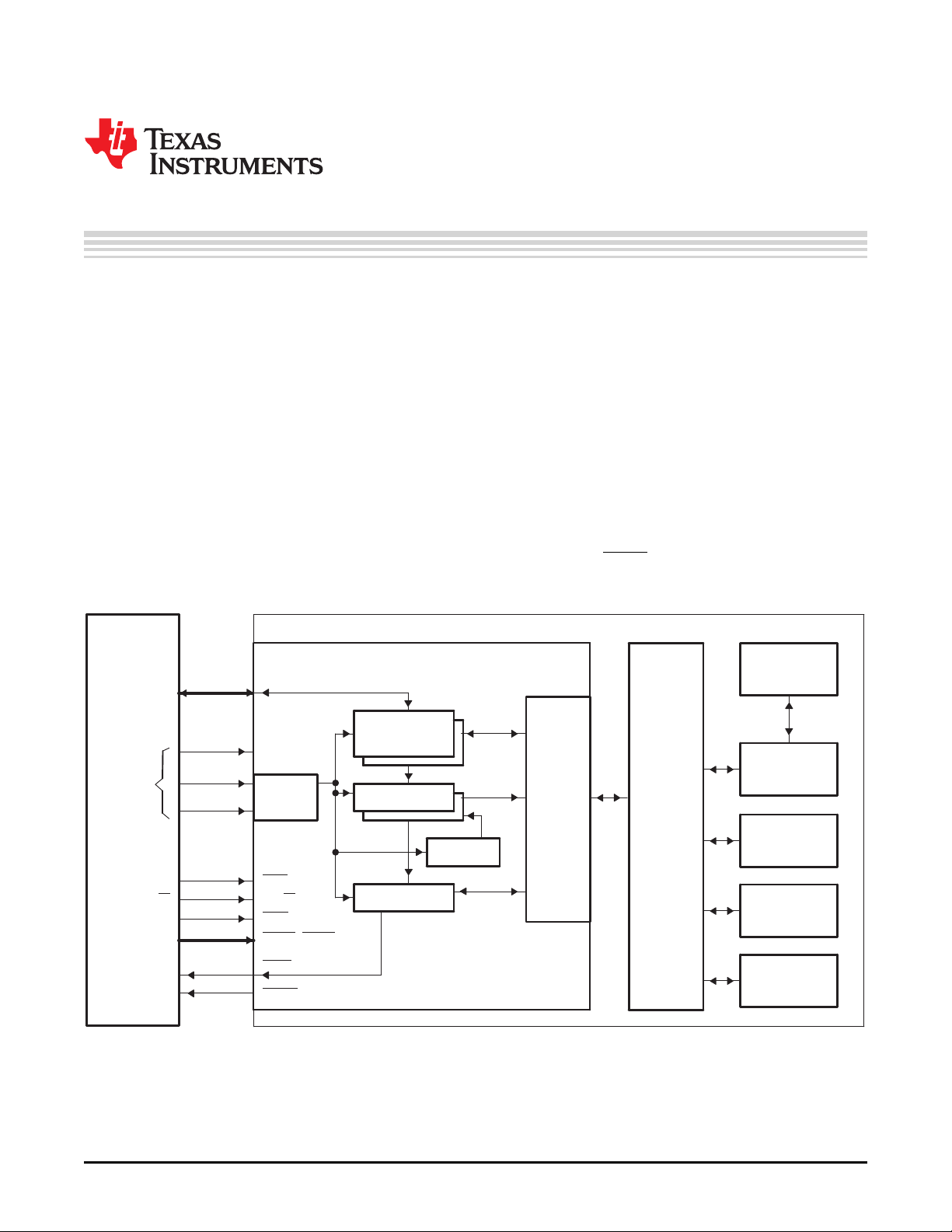
This guide describes the host port interface (HPI) on the TMS320C6457 digital signal processors (DSPs).
The HPI enables an external host processor (host) to directly access DSP resources (including internal
and external memory) using a 16-bit (HPI16) or 32-bit (HPI32) interface.
1 Introduction to the HPI
The HPI provides a parallel port interface through which an external host processor (host) can access
DSP resources. The HPI enables a host device and CPU to exchange information via internal or external
memory. Dedicated address and data registers (HPIA and HPID respectively) within the HPI provide the
data path between the external host interface and the processor resources. An HPI control register (HPIC)
is available to the host and the CPU for various configuration and interrupt functions.
Figure 1 is a high-level block diagram showing how the HPI connects a host (left side of figure) and the
DSP internal resources (right side of figure). The host functions as a master to the HPI. Host activity is
asynchronous to the internal clock that drives the HPI. When HPI resources are temporarily busy or
unavailable, the HPI informs the host by deasserting the HPI-ready (HRDY) output signal.
User's Guide
SPRUGK7A–March 2009–Revised July 2010
Host Port Interface (HPI)
Figure 1. HPI Position in the Host-DSP System
SPRUGK7A–March 2009–Revised July 2010 Host Port Interface (HPI)
Copyright © 2009–2010, Texas Instruments Incorporated
7
Page 8

Introduction to the HPI
The HPI uses multiplexed operation, meaning the data bus carries both address and data. When the host
drives an address on the bus, the address is stored in the address register (HPIA) in the HPI, so that the
bus can then be used for data.
The HPI supports two interface modes: HPI16 and HPI32 mode. DSP selects either HPI16 or HPI32 mode
via the HPI_WIDTH device configuration pin at reset.
• 16-bit multiplexed mode (HPI16). The HPI is called HPI16 when operating as a 16-bit wide host port.
This mode is selected if the HPI_WIDTH configuration pin of the DSP is sampled low at reset. In this
mode, a 16-bit data bus (HD[15:0]) carries both addresses and data. HPI16 combines successive
16-bit transfers to provide 32-bit data to the CPU. The halfword identification line (HHWIL) input is
used on the HPI16 to identify the first or second half word of a word transfer.
• 32-bit multiplexed mode (HPI32). HPI operates in this mode as a 32-bit wide host port. This mode is
selected if the HPI_WIDTH configuration pin of the DSP is sampled high at reset. In this mode, a 32-bit
data bus (HD[31:0]) carries both addresses and data. HHWIL is not applicable for HPI32 mode.
The HPI contains two HPIAs (HPIAR and HPIAW), which can be used as separate address registers for
read accesses and write accesses (for details, see Section 2).
A 32-bit control register (HPIC) is accessible by the DSP CPU and the host. The CPU can use HPIC to
send an interrupt request to the host, to clear an interrupt request from the host, and to monitor the HPI.
The host can use HPIC to configure and monitor the HPI, to send an interrupt request to the CPU, and to
clear an interrupt request from the CPU.
Data flow between the host and the HPI uses a temporary storage register, the 32-bit data register (HPID).
Data arriving from the host is held in HPID until the data can be stored elsewhere in the DSP. Data to be
sent to the host is held in HPID until the HPI is ready to perform the transfer. When address
autoincrementing is used, read and write FIFOs are used to store burst data. If autoincrementing is not
used, the FIFO memory acts as a single register (only one location is used).
www.ti.com
NOTE: To manage data transfers between HPID and the internal memory, the DSP contains
dedicated HPI DMA logic. The HPI DMA logic is not programmable. It automatically stores or
fetches data using the address provided by the host. The HPI DMA logic is independent of
the EDMA3 controller included in the DSP.
In the DSP system, master and slave peripherals communicate with each other via the Switched Central
Resource (SCR). By definition, master peripherals are capable of initiating read and write transfers in the
system and may not solely rely on the EDMA3 controller for their data transfers. Slave peripherals rely on
the EDMA3 controller to perform transfers. The HPI is a master peripheral; it uses its DMA logic to directly
communicate with the rest of the system via the SCR and does not rely on the EDMA3 controller for its
data transfers. Note that the HPI cannot access all DSP resources or peripherals; see the device-specific
data manual for a list of resources accessible through the HPI.
1.1 Summary of the HPI Registers
Table 1 summarizes the registers inside the HPI, including access permissions and access requirements
from the perspective of the host and the DSP CPU. See Section 8 for detailed descriptions of all these
registers. Section 2 describes the two address registers (HPIAW and HPIAR) and describes the two HPIA
modes that determine how the host uses these registers.
The host can only access HPIC, HPIAW, HPIAR, and HPID. By driving specific levels on the HCNTL[1:0]
signals, the host indicates whether it is performing an HPIC, HPIA, or HPID access. For an HPID access,
the HCNTL signals also indicate whether or not the HPI should perform an automatic address increment
after the access. Section 3.4 describes the effects of the HCNTL[1:0] signals. The HR/W signal indicates
whether the host is reading or writing.
The DSP CPU cannot access HPID but has limited access to HPIC, HPIAR, and HPIAW. The CPU has
full access to the power and emulation management register, which selects an emulation mode for the
HPI.
HPI registers accessible by the CPU have an address in the DSP memory map. Table 1 shows the offset
addresses for various HPI registers. See the device-specific data manual for the base addresses of the
HPI registers.
8
Host Port Interface (HPI) SPRUGK7A–March 2009–Revised July 2010
Copyright © 2009–2010, Texas Instruments Incorporated
Page 9

www.ti.com
(1)
Introduction to the HPI
Table 1. Summary of HPI Registers
Host Access CPU Access
Register Description Permissions Permissions Address
PWREMU_MGMT Power and Emulation None - Read/Write 04h
Management Register
HPIC Host Port Interface Control Read/Write HCNTL1 low Read: All bits 30h
Register HCNTL0 low Write: HINT
HPIAW Host Port Interface Write Address Read/Write HCNTL1 high Read only 34h
Register HCNTL0 low
HPIAR Host Port Interface Read Address Read/Write HCNTL1 high Read only 38h
Register HCNTL0 low
HPID Host Port Interface Data Register Read/Write With autoincrementing: None None
The single-HPIA mode and the dual-HPIA mode are described in Section 2.
Read/Write Access Requirements Read/Write Offset
and DSPINT
bits only
Single-HPIA mode, or
dual-HPIA mode with
HPIAW selected
Single-HPIA mode, or
dual-HPIA mode with
HPIAR selected
HCNTL1 low
HCNTL0 high
No autoincrementing:
HCNTL1 high
HCNTL0 high
(1)
(1)
1.2 Summary of the HPI Signals
Table 2 summarizes each of the HPI signals. It provides the signal name, the possible states for the signal
(input, output, or high-impedance), the connection(s) to be made on the host side of the interface, and a
description of the signal’s function.
Note that the encoding of HCNTL0 and HCNTL1 for the different types of HPI
accesses varies on many TI DSPs; therefore, you should use caution to ensure
that the correct encoding of these inputs is used for your device. The encoding
of these signals as described in this document applies only to C6457 DSPs.
Signal State
HCS I Chip select pin HPI chip select. HCS must be low for the HPI to be
HDS1 and I Read strobe and write strobe pins or HPI data strobe pins. These pins are used for strobing
HDS2 any data strobe pin data in and out of the HPI (for data strobing details,
(1)
Host Connection Description
CAUTION
Table 2. HPI Signals
selected by the host. HCS can be kept low between
accesses. HCS normally precedes an active HDS (data
strobe) signal, but can be connected to an HDS pin for
simultaneous select and strobe activity.
see Section 3.3). The direction of the data transfer
depends on the logic level of the HR/W signal.
The HDS signals are also used to latch control
information (if HAS is tied high) on the falling edge.
During an HPID write access, data is latched into the
HPID register on the rising edge of HDS. During read
operations, these pins act as output-enable pins of the
host data bus.
(1)
I = Input, O = Output, Z = High Impedance.
SPRUGK7A–March 2009–Revised July 2010 Host Port Interface (HPI)
Copyright © 2009–2010, Texas Instruments Incorporated
9
Page 10

Introduction to the HPI
Signal State
HCNTL[1:0] I Address or control pins The HPI latches the logic levels of these pins on the
HR/W I R/W strobe pin HPI read/write. On the falling edge of HAS or internal
HHWIL I Address or control pins Halfword identification control input. This bit identifies
HAS I ALE (address latch enable) or Address strobe. A host with a multiplexed address/data
HD[31:0] I/O/Z Data bus The HPI data bus carries the data to/from the HPI.
HD[15:0] HD[31:0] applies to HPI32 and HD[15:0] applies to
HRDY O/Z Asynchronous ready pin When the HPI drives HRDY low, the host has
HINT O/Z Interrupt pin The DSP can interrupt the host processor by writing a
www.ti.com
Table 2. HPI Signals (continued)
(1)
Host Connection Description
falling edge of HAS or internal HSTRB (for details
about internal HSTRB, see Section 3.3). The four
binary states of these pins determine the access type
of the current transfer (HPIC, HPID with
autoincrementing, HPIA, or HPID without
autoincrementing).
HSTRB, HR/W indicates whether the current access is
to be a read or write operation. Driving HR/W high
indicates the transfer is a read from the HPI, while
driving HR/W low indicates a write to the HPI.
the first and second halfwords of a dual halfword cycle
operation. HHWIL=0 identifies the first cycle and
HHWIL=1 identifies the second cycle. HHWIL applies
only to HPI16 mode and not to HPI32 mode.
address strobe pin bus can have HAS connected to its ALE pin. The
falling edge of HAS latches the logic levels of the
HR/W, HCNTL1, and HCNTL0 pins, which are typically
connected to host address lines. When used, the HAS
signal must precede the falling edge of the internal
HSTRB signal.
HPI16.
permission to complete the current host cycle. When
the HPI drives HRDY high, the HPI is not ready for the
current host cycle to complete.
1 to the HINT bit of HPIC. Before subsequent HINT
interrupts can occur, the host must clear previous
interrupts by writing a 1 to the HINT bit. This pin is
active-low and inverted from the HINT bit value in
HPIC.
10
Host Port Interface (HPI) SPRUGK7A–March 2009–Revised July 2010
Copyright © 2009–2010, Texas Instruments Incorporated
Page 11

www.ti.com
2 Using the Address Registers
The HPI contains two 32-bit address registers: one for read operations (HPIAR) and one for write
operations (HPIAW). These roles are unchanging from the position of the HPI DMA logic. HPI DMA logic
collects the address from HPIAR when reading from DSP internal/external memory and collects the
address from HPIAW when writing to DSP internal/external memory.
However, unlike the HPI DMA logic, the host can choose how to interact with the two HPIA registers.
Using the DUALHPIA bit of HPIC, the host determines whether HPIAR and HPIAW act as a single 32-bit
register (single-HPIA mode) or as two independent 32-bit registers (dual-HPIA mode).
The host must always write a word address to the HPIAs. For example, L2
memory has a base byte address of 80 0000h that corresponds to a word
address of 20 0000h. A host must write 20 0000h to the HPIA register to point
the HPI to the base of L2 memory.
2.1 Single-HPIA Mode
If DUALHPIA = 0 in HPIC, HPIAR and HPIAW become a single HPIA register for the host. In this mode:
• A host HPIA write cycle (HCNTL[1:0] = 10b, HR/W = 0) updates HPIAR and HPIAW with the same
value.
• Both HPIA registers are incremented during autoincrement read/write cycles (HCNTL[1:0] = 01b).
• An HPIA read cycle (HCNTL[1:0] = 10b, HR/W = 1) returns the contents of HPIAR, which should be
identical to the contents of HPIAW.
To maintain consistency between the contents of HPIAR and HPIAW, the host should always re-initialize
the HPIA registers after changing the state of the DUALHPIA bit. In addition, when DUALHPIA = 0, the
host must always re-initialize the HPIA registers when it changes the data direction (from an HPID read
cycle to an HPID write cycle, or vice versa). Otherwise, the memory location accessed by the HPI DMA
logic might not be the host's intended location.
Using the Address Registers
CAUTION
2.2 Dual-HPIA Mode
The host can take advantage of two independent HPIA registers by choosing the dual-HPIA mode
(DUALHPIA = 1 in HPIC). In this mode:
• A host HPIA access (HCNTL[1:0] = 10b) reads/updates either HPIAR or HPIAW, depending on the
value of the HPIA read/write select (HPIARWSEL) bit of HPIC. This bit is programmed by the host.
While HPIARWSEL = 1, only HPIAR is read or updated by the host. While HPIARWSEL = 0, only
HPIAW is read or updated by the host. The HPIARWSEL bit is only meaningful in the dual-HPIA mode.
NOTE: The HPIARWSEL bit does not affect the HPI DMA logic. Regardless of the value of
HPIARWSEL, the HPI DMA logic uses HPIAR when reading from memory and HPIAW when
writing to memory.
• A host HPID access with autoincrementing (HCNTL[1:0] = 01b) causes only the relevant HPIA value to
be incremented to the next consecutive memory address. In an autoincrement read cycle, HPIAR is
incremented after it has been used to perform the current read from memory. In an autoincrement write
cycle, HPIAW is incremented after it has been used for the write operation.
SPRUGK7A–March 2009–Revised July 2010 Host Port Interface (HPI)
Copyright © 2009–2010, Texas Instruments Incorporated
11
Page 12
Address or I/O
Read/Write
Chip select
Data strobe
A
Data/address
Interrupt
Ready
HCNTL[1:0]
HR/W
HCS
HDS1
HDS2
HD[31:0]
HINT
HRDY
HPI
Host
Address latch enable HAS
No connect HHWIL
Logic high
2
32
DSP
HPI Operation
3 HPI Operation
3.1 Host-HPI Signal Connections
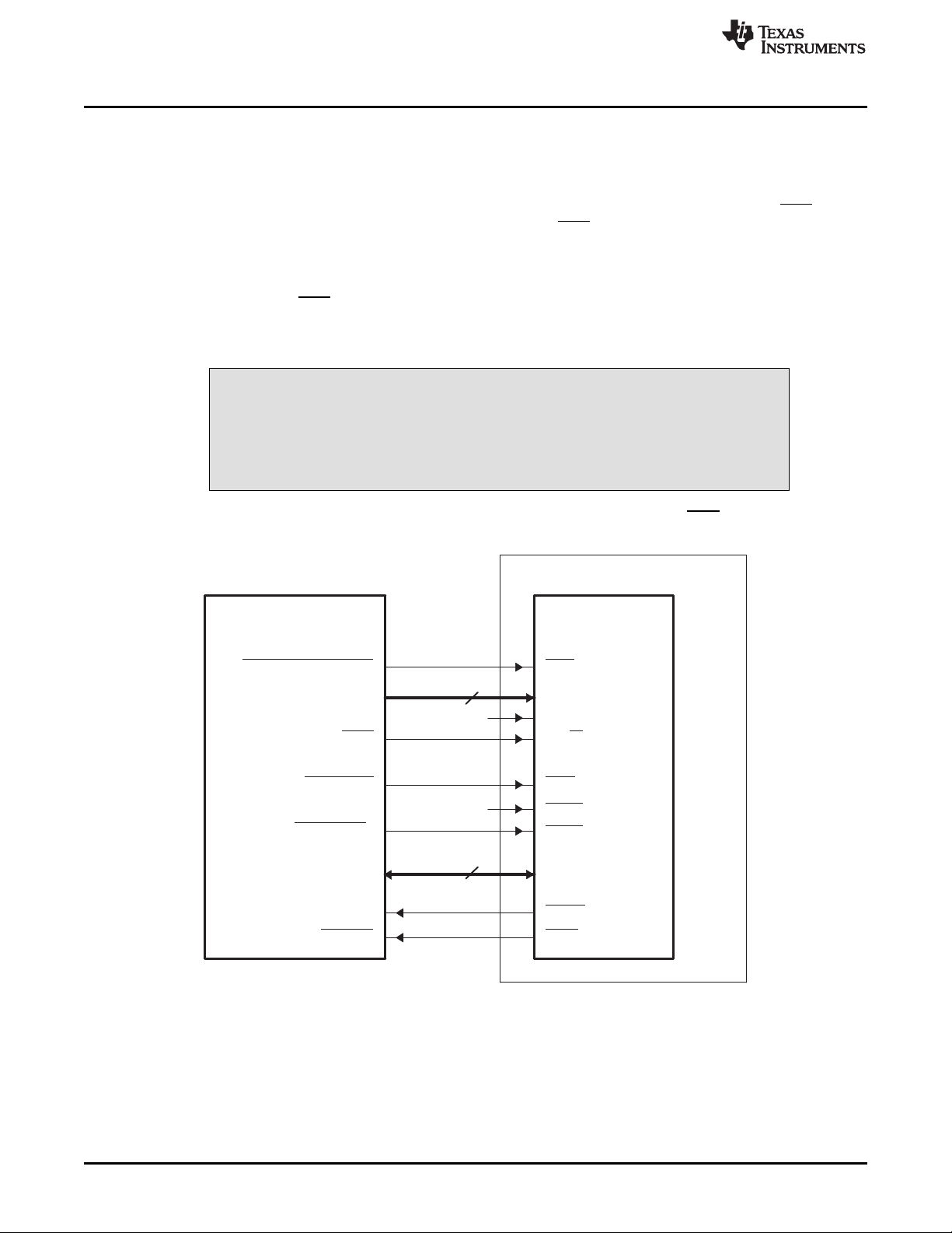
Figure 2 and Figure 3 show examples of signal connections for the 32-bit multiplexed mode. Figure 4 and
Figure 5 show similar examples for the 16-bit multiplexed mode. In Figure 2 and Figure 4, the HAS signal
is used as described in Section 3.6. In Figure 3 and Figure 5, HAS is tied high (not used). Note the
following key comparisons between the signal connections in the two interface modes:
• The HPI_WIDTH configuration pin of the DSP must be held high at reset for the 32-bit multiplexed
mode (HPI32) or low at reset for the 16-bit multiplexed mode (HPI16).
• The address strobe (HAS) of the HPI is optional for both modes.
• The halfword identification control line (HHWIL) of the HPI is not used in the 32-bit multiplexed mode,
but is required in the 16-bit multiplexed mode.
Note that the encoding of HCNTL0 and HCNTL1 for the different types of HPI
accesses varies on many TI DSPs; therefore, you should use caution to ensure
that the correct encoding of these inputs is used for your device. The encoding
of these signals as described in this document applies only to C6457 DSPs.
Figure 2. Example of Host-DSP Signal Connections When Using the HAS Signal
www.ti.com
CAUTION
in the 32-Bit Multiplexed Mode
A Data strobing options are given in Section 3.3.
12
Host Port Interface (HPI) SPRUGK7A–March 2009–Revised July 2010
Copyright © 2009–2010, Texas Instruments Incorporated
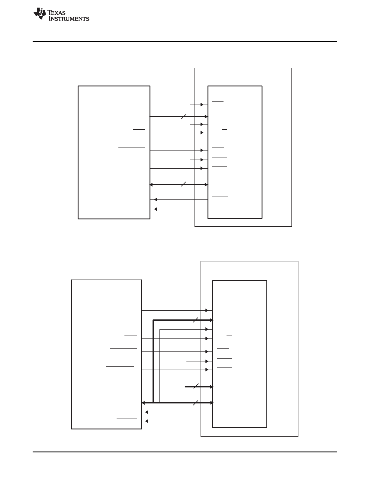
Page 13
Address or I/O
Read/Write
Chip select
Data strobe
A
Data/address
Interrupt
Ready
HCNTL[1:0]
HR/W
HCS
HDS1
HDS2
HD[31:0]
HINT
HRDY
HPIHost
Logic high HAS
No connect HHWIL
Logic high
2
32
DSP
Read/Write
Chip select
Data strobe
A
Data/address
Interrupt
Ready
HCNTL[1:0]
HR/W
HCS
HDS1
HDS2
HD[15:0]
HINT
HRDY
HPI
DSP
Host
Address latch enable HAS
HHWIL
Logic
high
HD[31:16]
No
connect
2
16
16
www.ti.com
HPI Operation
Figure 3. Example of Host-DSP Signal Connections When the HAS Signal is Tied High
in the 32-Bit Multiplexed Mode
A Data strobing options are given in Section 3.3.
Figure 4. Example of Host-DSP Signal Connections When Using the HAS Signal
in the 16-Bit Multiplexed Mode
A Data strobing options are given in Section 3.3.
SPRUGK7A–March 2009–Revised July 2010 Host Port Interface (HPI)
Copyright © 2009–2010, Texas Instruments Incorporated
13
Page 14

Read/Write
Chip select
Data strobe
A
Data
Interrupt
Ready
HCNTL[1:0]
HR/W
HCS
HDS1
HDS2
HD[15:0]
HINT
HRDY
HPI
DSP
Host
HAS
HHWIL
Logic high
Logic high
Address
or I/O
HD[31:16]No connect
2
16
16
HPI Operation
Figure 5. Example of Host-DSP Signal Connections When the HAS Signal is Tied High in the 16-Bit
Multiplexed Mode
www.ti.com
A Data strobing options are given in Section 3.3.
3.2 HPI Configuration and Data Flow
In multiplexed mode, the HPIC and HPIA must be initialized before valid host access cycles can take
place. The CPU and host must follow these steps to configure the HPI initially:
1. The CPU clears the HPIRST bit in the HPI register. All host accesses will be held off by the
deassertion of HRDY until HPIRST is cleared.
2. After the HPIRST bit is cleared, the host writes the HPIC register to program the halfword ordering bit
(HWOB) and the HPIA-related bits (DUALHPIA and HPIARWSEL). The HWOB bit must be
programmed before any accesses to the HPID and HPIA registers because this bit defines the
ordering of all halfword accesses in the 16-bit multiplexed mode.
3. The host writes the desired internal DSP word address to an address register (HPIAR and/or HPIAW).
Section 2 introduces the two HPIA registers and their interaction with the host.
4. The host either reads from or writes to the data register (HPID). Data transfers between HPID and the
internal resources of the DSP are handled by the HPI DMA logic.
Each step of the access uses the same bus. Therefore, the host must drive the appropriate levels on the
HCNTL1 and HCNTL0 signals to indicate which register is to be accessed. The host must also drive the
appropriate level on the HR/W signal to indicate the data direction (read or write) and must drive other
control signals as appropriate. When HPI resources are temporarily busy or unavailable, the HPI informs
the host by deasserting the HPI-ready (HRDY) output signal.
When performing an access, the HPI first latches the levels on HCNTL[1:0], HR/W, and other control
signals. This latching can occur on the falling edge of the internal strobe signal (see Section 3.3) or the
falling edge of HAS (see Section 3.6). After the control information is latched, the HPI initiates an access
based on the control signals.
14
Host Port Interface (HPI) SPRUGK7A–March 2009–Revised July 2010
Copyright © 2009–2010, Texas Instruments Incorporated
Page 15
HDS1
HDS2
HCS
HRDY
Internal
HSTRB
Internal
HRDY
www.ti.com
If the host wants to read data from the DSP internal/external memory, the HPI DMA logic reads the
memory address from HPIAR and retrieves the data from the addressed memory location. When the data
has been placed in HPID, the HPI drives the data onto its HD bus. The HRDY signal informs the host
whether the data on the HD bus is valid (HRDY low) or not valid yet (HRDY high). When the data is valid,
the host latches the data and drives the connected data strobe (HDS1 or HDS2) inactive, which, in turn,
will cause the internal strobe (internal HSTRB) signal to transition from low to high.
If the host wants to write data to the DSP internal/external memory, the operation is similar. After the host
determines that the HPI is ready to latch the data (HRDY is low), it must cause internal HSTRB to
transition from low to high, which causes the data to be latched into HPID. Once the data is in HPID, the
HPI DMA logic reads the memory address from HPIAW and transfers the data from HPID to the
addressed memory location.
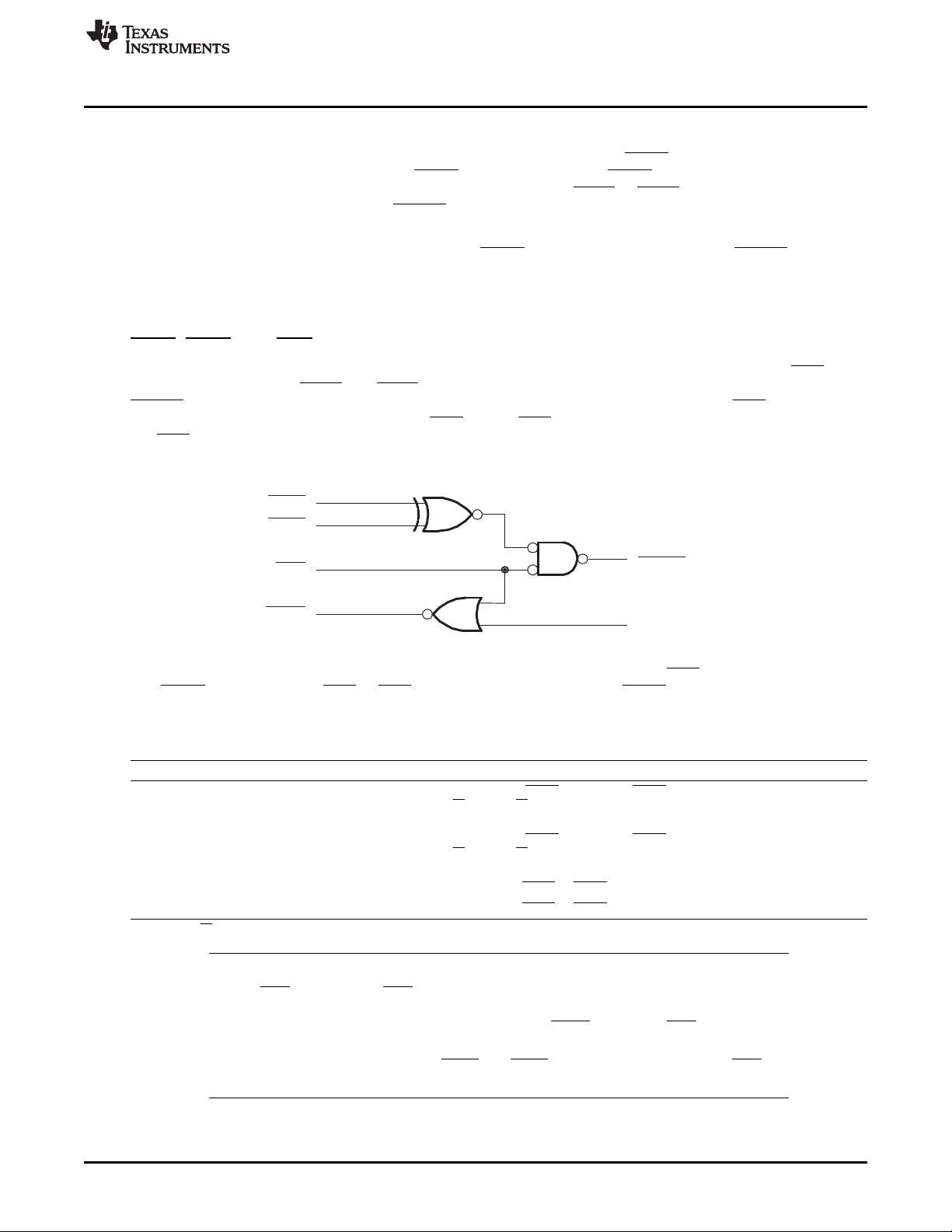
3.3 HDS2, HDS1, and HCS: Data Strobing and Chip Selection
As illustrated in Figure 6, the strobing logic is a function of three key inputs: the chip select pin (HCS) and
two data strobe signals (HDS1 and HDS2). The internal strobe signal, which is referred to as internal
HSTRB throughout this document, functions as the actual strobe signal inside the HPI. HCS must be low
(HPI selected) during strobe activity on the HDS pins. If HCS remains high (HPI not selected), activity on
the HDS pins is ignored.
Figure 6. HPI Strobe and Select Logic
HPI Operation
Strobe connections between the host and the HPI partially depend on the number and types of strobe pins
available on the host. Table 3 describes various options for connecting to the HDS pins. Notice in Figure 6
that HRDY is also gated by HCS. If HCS goes high (HPI not selected), HRDY goes low, regardless of
whether the current internal transfer is completed in the DSP.
Table 3. Options for Connecting Host and HPI Data Strobe Pins
Available Host Data Strobe Pins Connections to HPI Data Strobe Pins
Host has separate read and write strobe Connect one strobe pin to HDS1 and other to HDS2
pins, both active-low provide an R/W line, HR/W timings must be satisfied as stated in the device datasheet,
Host has separate read and write strobe Connect one strobe pin to HDS1 and other to HDS2
pins, both active-high provide an R/W line, HR/W timings must be satisfied as stated in the device datasheet,
Host has one active-low strobe pin Connect the strobe pin to HDS1 or HDS2, and connect the other pin to logic level 1.
Host has one active-high strobe pin Connect the strobe pin to HDS1 or HDS2, and connect the other pin to logic level 0.
(1)
The HR/W signal could be driven by a host address line in this case.
perhaps by using a host address line.
perhaps by using a host address line.
NOTE:
1. The HCS input and one HDS strobe input can be tied together and driven with a single
strobe signal from the host. This technique selects the HPI and provides the strobe
simultaneously. When using this method, note that HRDY is gated by HCS as previously
described.
2. It is not recommended to tie both HDS1 and HDS2 to static logic levels and use HCS as
a strobe.
SPRUGK7A–March 2009–Revised July 2010 Host Port Interface (HPI)
(1)
. Because such a host might not
(1)
. Because such a host might not
15
Copyright © 2009–2010, Texas Instruments Incorporated
Page 16

HPI Operation
3.4 HCNTL[1:0] and HR/W: Indicating the Cycle Type
The cycle type consists of:
• The access type selected by the host by driving the appropriate levels on the HCNTL[1:0] pins of the
HPI. Table 4 describes the four available access types.
• The transfer direction that the host selects with the HR/W pin. The host must drive the HR/W signal
high (read) or low (write).
Table 5 summarizes the cycle types. The HPI samples the HCNTL levels either at the falling edge of HAS
(if HAS is used) or at the falling edge of the internal strobe signal HSTRB (if HAS is not used or is tied
high).
CAUTION
Note that the encoding of HCNTL0 and HCNTL1 for the different types of HPI
accesses varies on many TI DSPs; therefore, you should use caution to ensure
that the correct encoding of these inputs is used for your device. The encoding
of these signals as described in this document applies only to C6457 DSPs.
Table 4. Access Types Selectable by the HCNTL Signals
HCNTL1 HCNTL0 Description
0 0 HPIC access. The host requests to access the HPI control register
(HPIC).
0 1 HPID access with autoincrementing. The host requests to access the
HPI data register (HPID) and to have the appropriate HPI address
register (HPIAR and/or HPIAW) automatically incremented by 1 after
the access.
1 0 HPIA access. The host requests to access the appropriate HPI
address register (HPIAR and/or HPIAW).
1 1 HPID access without autoincrementing. The host requests to access
the HPI data register (HPID) but requests no automatic
post-increment of the HPI address register.
www.ti.com
16
Table 5. Cycle Types Selectable With the HCNTL and HR/W Signals
HCNTL1 HCNTL0 HR/W Cycle Type
0 0 0 HPIC write cycle
0 0 1 HPIC read cycle
0 1 0 HPID write cycle with autoincrementing
0 1 1 HPID read cycle with autoincrementing
1 0 0 HPIA write cycle
1 0 1 HPIA read cycle
1 1 0 HPID write cycle without
autoincrementing
1 1 1 HPID read cycle without
autoincrementing
Host Port Interface (HPI) SPRUGK7A–March 2009–Revised July 2010
Copyright © 2009–2010, Texas Instruments Incorporated
Page 17

www.ti.com
3.5 HHWIL: Identifying the First and Second Halfwords in 16-Bit Multiplexed Mode
In the 16-bit multiplexed mode, each host cycle consists of two consecutive halfword transfers. For each
transfer, the host must specify the cycle type with HCNTL[1:0] and HR/W, and the host must use HHWIL
to indicate whether the first or second halfword is being transferred. For HPID and HPIA accesses, HHWIL
must always be driven low for the first halfword transfer and high for the second halfword transfer. Results
are undefined if the sequence is broken. For examples of HHWIL usage, see the figures in Section 3.6
and Section 3.7.
When the host sends the two halfwords of a 32-bit word in this manner, the host can send the most and
least significant halfwords of the 32-bit word in either order (most significant halfword first or most
significant halfword second). However, the host must inform the HPI of the selected order before
beginning the host cycle. This is done by programming the halfword order (HWOB) bit of HPIC. Although
(HWOB) is written at bit 0 in HPIC, its current value is readable at both bit 0 and bit 8 (HWOBSTAT).
Thus, the host can determine the current halfword-order configuration by checking the least significant bit
of either half of HPIC.
There is one case when the 16-bit multiplexed mode does not require a dual-halfword cycle with HHWIL
low for the first halfword and HHWIL high for the second halfword. The least significant 16 bits of the HPIC
register can be accessed with a single-halfword cycle. During such a cycle, the host can drive HHWIL
either high or low. Either approach returns the same value. Section 3.9 includes an example timing
diagram of this case.
In the 32-bit multiplexed mode, each host cycle is one word transfer. The HHWIL signal is ignored and 32
bits of data transferred for each active cycle of the internal strobe signal (internal HSTRB).
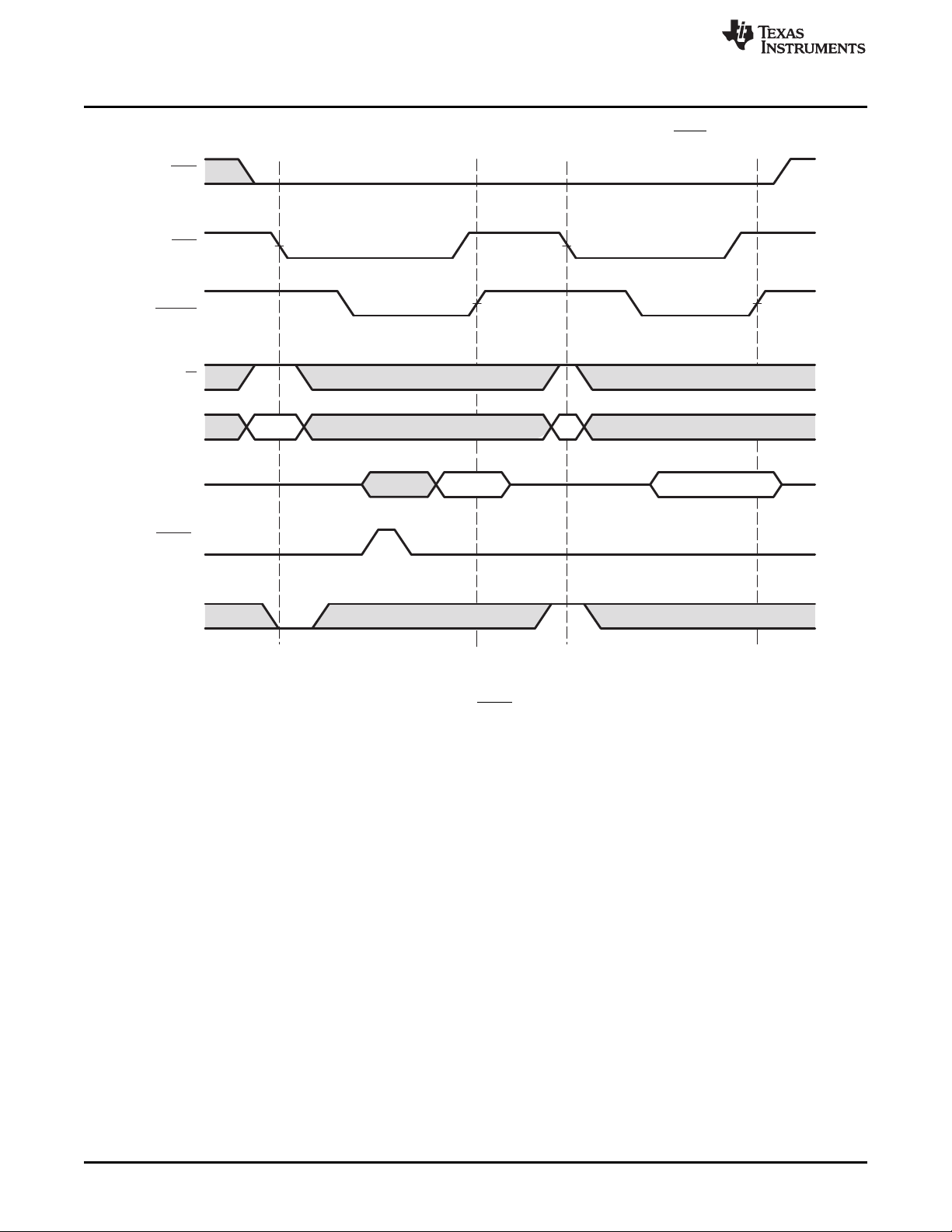
3.6 HAS: Forcing the HPI to Latch Control Information Early
HPI Operation
The HAS signal is an address strobe that allows control information to be removed earlier in a host cycle,
allowing more time to switch bus states from address to data information. This feature facilitates the
interface for multiplexed address and data buses. In this type of system, an address latch enable (ALE)
signal is often provided and is normally the signal connected to HAS.
Figure 2 and Figure 4 show examples of signal connections when HAS is used for multiplexed transfers.
Figure 7 and Figure 8 show typical HPI signal activity when HAS is used. The process for using HAS is as
follows:
1. The host selects the access type. The host drives the appropriate levels on the HCNTL [1:0] and HR/W
signals, and indicates which halfword (first or second) will be transferred by driving HHWIL high or low.
2. The host drives HAS low. On the falling edge of HAS, the HPI latches the states of the HCNTL[1:0],
HR/W, and HHWIL. The high to low transition of HAS must precede the falling edge of the internal
strobe signal (internal HSTRB), which is derived from HCS, HDS1, and HDS2, as described in
Section 3.3.
HCS does not gate the HAS input, which allows time for the host to perform the subsequent access. The
HAS signal may be brought high after internal HSTRB goes low, indicating that the data access is about to
occur. HAS is not required to be driven high at any time during the cycle, but eventually must transition
high before the host uses it for another access with different values for HCNTL [1:0], HR/W, and HHWIL.
SPRUGK7A–March 2009–Revised July 2010 Host Port Interface (HPI)
Copyright © 2009–2010, Texas Instruments Incorporated
17
Page 18
Data 2Data 1
HCS
HAS
HSTRB
HR/W
HCNTL[1:0]
HD[15:0]
HRDY
A
HHWIL
Internal
HPI latches
control information
Host latches
data
HPI latches
control information
Host latches
data
HPI Operation
www.ti.com
Figure 7. 16-Bit Multiplexed Mode Host Read Cycle Using HAS
A Depending on the type of write operation (HPID without autoincrementing, HPIA, HPIC, or HPID with
autoincrementing) and the state of the FIFO, transitions on HRDY may or may not occur. For more information, see
Section 3.9.
18
Host Port Interface (HPI) SPRUGK7A–March 2009–Revised July 2010
Copyright © 2009–2010, Texas Instruments Incorporated
Page 19

HCS
HAS
HSTRB
HR/W
HCNTL[1:0]
HRDY
A
HHWIL
Data 1 Data 2
HD[15:0]
Internal
HPI latches
control information
HPI latches
data
HPI latches
control information
HPI latches
data
www.ti.com
HPI Operation
Figure 8. 16-Bit Multiplexed Mode Host Write Cycle Using HAS
A Depending on the type of write operation (HPID without autoincrementing, HPIA, HPIC, or HPID with
autoincrementing) and the state of the FIFO, transitions on HRDY may or may not occur. For more information, see
Section 3.9.
SPRUGK7A–March 2009–Revised July 2010 Host Port Interface (HPI)
Copyright © 2009–2010, Texas Instruments Incorporated
19
Page 20

Data 2Data 1
HCS
HSTRB
HR/W
HCNTL[1:0]
HD[15:0]
HRDY
A
HHWIL
Internal
HPI latches
control information
Host latches
data
HPI latches
control information
Host latches
data
HPI Operation
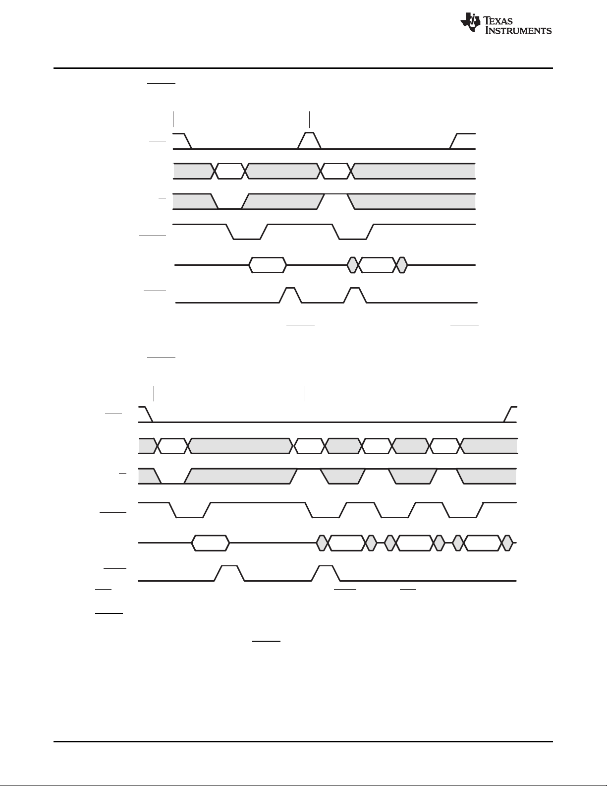
3.7 Performing a Multiplexed Access Without HAS
The HAS signal is not required when the host processor has dedicated signals (address lines or bit I/O)
capable of driving the control lines. Dedicated pins can be directly connected to HCNTL[1:0], HR/W, and
HHWIL.
Figure 3 and Figure 5 show examples of signal connections when HAS is not used for multiplexed
transfers. When HAS is not used, it must be tied high (inactive). Figure 9 and Figure 10 show typical HPI
signal activity when HAS is tied high. The falling edge of internal HSTRB latches the HCNTL[1:0], HR/W,
and HHWIL states into the HPI. Internal HSTRB is derived from HCS, HDS1, and HDS2, as described in
Section 3.3.
Figure 9. 16-Bit Multiplexed Mode Host Read Cycle With HAS Tied High
www.ti.com
A Depending on the type of write operation (HPID without autoincrementing, HPIA, HPIC, or HPID with
autoincrementing) and the state of the FIFO, transitions on HRDY may or may not occur. For more information, see
Section 3.9.
20
Host Port Interface (HPI) SPRUGK7A–March 2009–Revised July 2010
Copyright © 2009–2010, Texas Instruments Incorporated
Page 21

HCS
HSTRB
HRDY
A
HR/W
HCNTL[1:0]
HHWIL
Data 1 Data 2
HD[15:0]
Internal
HPI latches
control information
HPI latches
data
HPI latches
control information
HPI latches
data
www.ti.com
HPI Operation
Figure 10. 16-Bit Multiplexed Mode Host Write Cycle With HAS Tied High
A Depending on the type of write operation (HPID without autoincrementing, HPIA, HPIC, or HPID with
autoincrementing) and the state of the FIFO, transitions on HRDY may or may not occur. For more information, see
Section 3.9.
SPRUGK7A–March 2009–Revised July 2010 Host Port Interface (HPI)
Copyright © 2009–2010, Texas Instruments Incorporated
21
Page 22

Data 1
HCS
HSTRB
HR/W
HCNTL[1:0]
HD[15:0]
HRDY
HHWIL
Internal
Valid
00
Valid
HPI Operation
3.8 Single-Halfword HPIC Cycle in the 16-Bit Multiplexed Mode
In 16-bit multiplexed mode, the lower 16 bits of the HPIC registers are duplicated on the upper 16 bits
during HPIC host accesses. Therefore, the host only needs to perform a single halfword cycle access to
read the HPIC register. The host can drive the HHWIL pin either high or low, and either approach returns
the same value. Figure 11 shows the special case in which the host performs a single-halfword cycle to
access the HPIC (see Section 3.5). Although the example in Figure 11 has the HAS signal tied high, this
type of HPIC cycle can also be done using the HAS signal to force early latching of control information.
Figure 11. 16-Bit Multiplexed Mode Single-Halfword HPIC Cycle with HAS Tied High
www.ti.com
3.9 Hardware Handshaking Using the HPI-Ready (HRDY) Signal
The HPI ready signal HRDY indicates to the host whether the HPI is ready to complete an access. During
a read cycle, the HPI is ready (drives HRDY low) when it has data available for the host. During a write
cycle, the HPI is ready (drives HRDY low) when it is ready to latch data from the host. If the HPI is not
ready, it can drive HRDY high to insert wait states. These wait states indicate to the host that read data is
not yet valid (read cycle) or that the HPI is not ready to latch write data (write cycle). The number of wait
states that must be inserted by the HPI is dependent upon the state of the accessed resource. See the
device-specific data manual for more information.
NOTE: In some cases, if the host does not have an input pin to connect to the HRDY pin, the host
can check the readiness of the HPI by polling the HRDY bit in the control register (HPIC).
For details, see Section 4.
22
When the HPI is not ready to complete the current cycle (HRDY high), the host can begin a new host
cycle by forcing the HPI to latch new control information. However, once the cycle has been initiated, the
host must wait until HRDY goes low before causing a rising edge on the internal strobe signal (internal
HSTRB) to complete the cycle. If internal HSTRB goes high when the HPI is not ready, the cycle will be
terminated with invalid data being returned (read cycle) or written (write cycle).
One reason the HPI may drive HRDY high is a not-ready condition in one of its first-in, first-out buffers
(FIFOs). For example, any HPID access that occurs while the write FIFO is full or the read FIFO is empty
may result in some number of wait states being inserted by the HPI. The FIFOs are explained in
Section 6.
Host Port Interface (HPI) SPRUGK7A–March 2009–Revised July 2010
Copyright © 2009–2010, Texas Instruments Incorporated
Page 23

1st halfword
00 or 10 00 or 10
2nd halfword
Internal
HD[15:0]
HRDY
HHWIL
HR/W
HCNTL[1:0]
HCS
HSTRB
HCS
HCNTL[1:0]
HR/W
HHWIL
Internal
HSTRB
HD[15:0]
HRDY
1st halfword 2nd halfword 1st halfword
2nd halfword
11 111010
HPIA write HPID read
HCS
Internal
HRDY
HD[15:0]
HR/W
HCNTL[1:0]
HHWIL
10 10 01 01 01
1st halfword2nd halfword1st halfword2nd halfword1st halfword
HSTRB
HPIA write HPID+ reads
www.ti.com
The following sections describe the behavior of HRDY during HPI register accesses. In all cases, the chip
select signal, HCS, must be asserted for HRDY to go high.
3.9.1 HRDY Behavior During 16-Bit Multiplexed Read Operations
Figure 12 shows an HPIC (HCNTL[1:0] = 00b) or HPIA (HCNTL[1:0] = 10b) read cycle during 16-bit
multiplexed HPI operation. Neither an HPIC read cycle nor an HPIA read cycle causes HRDY to go high.
Figure 12. HRDY Behavior During an HPIC or HPIA Read Cycle in the 16-Bit Multiplexed Mode
Figure 13 includes an HPID read cycle without autoincrementing in the 16-bit multiplexed mode. The host
writes the memory address during the HPIA (HCNTL[1:0] = 10b) write cycle, and the host reads the data
during the HPID (HCNTL[1:0] = 11b) read cycle. HRDY goes high for each HPIA halfword access, but
HRDY goes high for only the first halfword access in each HPID read cycle.
HPI Operation
Figure 13. HRDY Behavior During a Data Read Operation in the 16-Bit Multiplexed Mode
(Case 1: HPIA Write Cycle Followed by Nonautoincrement HPID Read Cycle)
Figure 14 includes an autoincrement HPID read cycle in the 16-bit multiplexed mode. The host writes the
memory address while asserting HCNTL[1:0] = 10b and reads the data while asserting HCNTL[1:0] = 01b.
During the first HPID read cycle, HRDY goes high for only the first halfword access, and subsequent HPID
read cycles do not cause HRDY to go high.
Figure 14. HRDY Behavior During a Data Read Operation in the 16-Bit Multiplexed Mode
(Case 2: HPIA Write Cycle Followed by Autoincrement HPID Read Cycles)
SPRUGK7A–March 2009–Revised July 2010 Host Port Interface (HPI)
Copyright © 2009–2010, Texas Instruments Incorporated
23
Page 24

1st halfword 2nd halfword
0000
Internal
HD[15:0]
HRDY
HHWIL
HR/W
HCNTL[1:0]
HCS
HSTRB
10 10 11 11
1st halfword 2nd halfword2nd halfword1st halfword
Internal
HSTRB
HD[15:0]
HRDY
HHWIL
HR/W
HCNTL[1:0]
HCS
HPIA write HPID write
10 10 01 01 01
1st halfword2nd halfword1st halfword2nd halfword1st halfword
Internal
HSTRB
HD[15:0]
HRDY
HHWIL
HR/W
HCNTL[1:0]
HCS
HPIA write HPID+ writes
HPI Operation
3.9.2 HRDY Behavior During 16-Bit Multiplexed Write Operations
Figure 15 shows an HPIC (HCNTL[1:0] = 00b) write cycle during 16-bit multiplexed HPI operation. An
HPIC write cycle does not cause HRDY to go high.
Figure 15. HRDY Behavior During an HPIC Write Cycle in the 16-Bit Multiplexed Mode
Figure 16 includes a HPID write cycle without autoincrementing in the 16-bit multiplexed mode. The host
writes the memory address while HCNTL[1:0] = 10b and writes the data while HCNTL[1:0] = 11b. During
the HPID write cycle, HRDY goes high only for the second halfword access.
Figure 16. HRDY Behavior During a Data Write Operation in the 16-Bit Multiplexed Mode
(Case 1: No Autoincrementing)
www.ti.com
Figure 17 shows autoincrement HPID write cycles in the 16-bit multiplexed mode when the write FIFO is
empty prior to the HPIA write. The host writes the memory address while HCNTL[1:0] = 10b and writes the
data while HCNTL[1:0] = 01b. HRDY does not go high during any of the HPID write cycles.
Figure 17. HRDY Behavior During a Data Write Operation in the 16-Bit Multiplexed Mode
(Case 2: Autoincrementing Selected, FIFO Empty Before Write)
Figure 18 shows a case similar to that of Figure 17. However, in Figure 18, the write FIFO is not empty
when the HPIA access is made. HRDY goes high twice for the first halfword access of the HPIA write
cycle. The first HRDY high period is due to the non-empty FIFO. The data currently in the FIFO must first
be written to the memory. This results in HRDY going high immediately after the falling edge of the data
strobe (HSTRB). The second and third HRDY high periods occur for the writes to the HPIA. HRDY
remains low for the HPID accesses.
24
Host Port Interface (HPI) SPRUGK7A–March 2009–Revised July 2010
Copyright © 2009–2010, Texas Instruments Incorporated
Page 25

10 10 01 01 01
1st halfword2nd halfword1st halfword2nd halfword1st halfword
Internal
HSTRB
HD[15:0]
HRDY
HHWIL
HR/W
HCNTL[1:0]
HCS
HPIA write HPID+ writes
00 or 10
HCNTL[1:0]
HD[31:0]
HRDY
HR/W
Internal
HSTRB
HCS
www.ti.com
Figure 18. HRDY Behavior During a Data Write Operation in the 16-Bit Multiplexed Mode
(Case 3: Autoincrementing Selected, FIFO Not Empty Before Write)
3.9.3 HRDY Behavior During 32-Bit Multiplexed Read Operations
Figure 19 shows an HPIC (HCNTL[1:0] = 00b) read or an HPIA (HCNTL[1:0] = 10b) read access for 32-bit
multiplexed HPI operation. Note that neither an HPIC nor an HPIA read access causes HRDY to become
active.
Figure 19. HRDY Behavior During an HPIC or HPIA Read Cycle in the 32-Bit Multiplexed Mode
HPI Operation
Figure 20 shows an HPIA (HCNTL[1:0] = 10b) write access followed by an HPID (HCNTL[1:0] = 11b) read
access for 32-bit multiplexed HPI operation.
SPRUGK7A–March 2009–Revised July 2010 Host Port Interface (HPI)
Copyright © 2009–2010, Texas Instruments Incorporated
25
Page 26
1110
HPIA Write HPID Read
HCNTL[1:0]
HD[31:0]
HRDY
HR/W
Internal
HSTRB
HCS
10 01 01 01
HPIA Write HPID+ Reads
HD[31:0]
HRDY
HCS
A
HCNTL[1:0]
HR/W
Internal
HSTRB
HPI Operation
Figure 20. HRDY Behavior During a Data Read Operation in the 16-Bit Multiplexed Mode
Figure 21 shows an HPIA (HCNTL[1:0] = 10b) write access followed by several autoincrement HPID
(HCNTL[1:0] = 01b) read accesses. Note that HRDY is active for the HPIA access. HRDY is also active
for the first HPID read access, but not for subsequent read accesses.
www.ti.com
(Case 1: HPIA Write Cycle Followed by Nonautoincrement HPID Read Cycle)
Figure 21. HRDY Behavior During a Data Read Operation in the 32-Bit Multiplexed Mode
(Case 2: HPIA Write Cycle Followed by Autoincrement HPID Read Cycles)
A HCSmay be brought high during strobe cycles. However, note that HRDY is gated by HCS.
3.9.4 HRDY Behavior During 32-Bit Multiplexed Write Operations
Figure 22 shows an HPIC (HCNTL[1:0] = 00b) write access for 32-bit multiplexed HPI operation. Note that
an HPIC write access does not cause HRDY to become active.
26
Host Port Interface (HPI) SPRUGK7A–March 2009–Revised July 2010
Copyright © 2009–2010, Texas Instruments Incorporated
Page 27
00
HCNTL[1:0]
HD[31:0]
HRDY
HR/W
Internal
HSTRB
HCS
10 11
HPIA Write HPID Write
HRDY
HR/W
Internal
HSTRB
HCS
HCNTL[1:0]
HD[31:0]
www.ti.com
Figure 23 shows an HPIA (HCNTL[1:0] = 10b) write access followed by an HPID (HCNTL[1:0] = 11b) write
access for 32-bit multiplexed HPI operation.
HPI Operation
Figure 22. HRDY Behavior During an HPIC Write Cycle in the 32-Bit Multiplexed Mode
Figure 23. HRDY Behavior During a Data Write Operation in the 32-Bit Multiplexed Mode
(Case 1: No Autoincrementing)
Figure 24 shows an HPIA (HCNTL[1:0] = 10b) write access followed by several autoincrementing HPID
(HCNTL[1:0] = 01b) write accesses when the write FIFO is empty. Note that HRDY is active during the
HPIA access but not active during any of the HPID accesses.
SPRUGK7A–March 2009–Revised July 2010 Host Port Interface (HPI)
Copyright © 2009–2010, Texas Instruments Incorporated
27
Page 28

10
01 01
01
HPIA Write HPID+ Writes
HCNTL[1:0]
HD[31:0]
HRDY
HR/W
Internal
HSTRB
HCS
A
10
01
01
01
HPIA Write HPID+ Writes
HD[31:0]
HRDY
Internal
HSTRB
HCS
A
HCNTL[1:0]
HR/W
HPI Operation
Figure 24. HRDY Behavior During a Data Write Operation in the 32-Bit Multiplexed Mode
(Case 2: Autoincrementing Selected, FIFO Empty Before Write)
A HCSmay be brought high during strobe cycles. However, note that HRDY is gated by HCS.
Figure 25 shows an HPIA (HCNTL[1:0] = 10b) write access when the write FIFO is not empty, followed by
several autoincrementing HPID (HCNTL[1:0] = 01b) write accesses. Note that HRDY is active twice for the
HPIA access. This occurs because the FIFO is not empty and the data in the FIFO must first be written to
memory. This results in an HRDY assertion immediately after the falling edge of the datastrobe (HSTRB).
When a write request to memory has been made that will empty the internal FIFO, the HPIA write
operation can complete with the rising edge of HSTRB. The second HRDY assertion is for the write to the
HPIA register. HRDY is not active for the HPID accesses.
www.ti.com
Figure 25. HRDY Behavior During a Data Write Operation in the 32-Bit Multiplexed Mode
(Case 3: Autoincrementing Selected, FIFO Not Empty Before Write)
A HCSmay be brought high during strobe cycles. However, note that HRDY is gated by HCS.
28
Host Port Interface (HPI) SPRUGK7A–March 2009–Revised July 2010
Copyright © 2009–2010, Texas Instruments Incorporated
Page 29

www.ti.com
Software Handshaking Using the HPI Ready (HRDY) Bit
4 Software Handshaking Using the HPI Ready (HRDY) Bit
In addition to the HRDY output signal, the HPI contains an HRDY bit in the control register (HPIC). This bit
is useful for software polling when the host does not have an input pin to connect to the HRDY pin. In
some cases, the host can read the HPIC register and, based on the status of the HRDY bit, determine
whether the HPI is ready with read data (during a read cycle) or ready to latch write data (during a write
cycle). Section 4.1 explains which read cycles and write cycles allow for polling of the HRDY bit.
NOTE: Software handshaking using the HRDY bit is not supported on all devices. See your
device-specific data manual to determine if this functionality is supported on your device.
When the host is performing HPID host cycles with an automatic address increment between accesses,
the value in the HRDY bit refers to the availability of space in the write FIFO or the availability of data in
the read FIFO. If the previous host cycle was a read cycle, the HRDY bit refers to the read FIFO. If the
previous host cycle was a write cycle, the HRDY bit refers to the write FIFO. If the previous host cycle set
the FETCH bit of HPIC, the HRDY bit refers to the read FIFO. If the host has performed no data accesses
yet, the HRDY bit refers to the write FIFO by default.
The HRDY bit reflects the level of an internal HRDY signal that is not gated by the chip select (HCS) input.
The HRDY bit could be cleared in response to one of the following conditions:
• A prefetch was issued (FETCH = 1 in HPIC). HRDY is low until a flush occurs and new data is loaded
in the read FIFO. When the data is available, the HRDY bit is set.
• The previous cycle was an autoincrement HPID write cycle, and the write FIFO became full. When
space is available in the write FIFO, the HRDY bit is set.
• The previous cycle was a non-autoincrement HPID write cycle and the write FIFO is not empty. This
condition indicates that the data has not yet been written to memory.
• The previous cycle was an HPID read cycle and the read FIFO is empty. Exception: If the previous
cycle was a non-autoincrement HPID read cycle, when internal HSTRB becomes high (inactive), the
HRDY bit stays 1 even though the FIFO is empty. This exception accommodates hosts that require the
HPI to indicate that it is ready before the host begins the next cycle.
• The previous cycle was an HPID read cycle and a read FIFO flush is in progress.
4.1 Polling the HRDY Bit
Read cycles. Only the FETCH command and autoincrement HPID read cycles may perform reads in this
mode while using HRDY polling. Fixed address mode HPID read cycles may not be performed because
during cycles in fixed address mode, the host must extend the read cycle until the read FIFO is flushed
and the read data is retrieved from the DSP memory. Therefore, the host cannot create the HPIC cycles
needed to poll HRDY because the host bus is busy with the current read access. The difference in a cycle
with autoincrementing is that the host can release the host bus while the read data is automatically loaded
into the read FIFO (due to the FETCH command and subsequent autoincrement read cycles).
Write cycles. As long as the HRDY bit is sampled high (and refers to write FIFO status), any type of write
cycle may be performed by the host. This includes autoincrement HPID write cycles and fixed address
mode HPID write cycle. It is possible to do either type of HPID cycle because the write data goes into the
FIFO, and the internal transfer to DSP memory takes place after the host has ended the host bus cycle.
This leaves the host bus inactive and available to the host for HPIC reads to poll the HRDY bit.
SPRUGK7A–March 2009–Revised July 2010 Host Port Interface (HPI)
Copyright © 2009–2010, Texas Instruments Incorporated
29
Page 30

DSPINT=0
DSPINT=1
CPU writes 1
to DSPINT bit
Interrupt
pending
Host writes 0
to DSPINT bit
No interrupt/
interrupt
cleared
Host writes 0 or 1
to DSPINT bit
CPU writes 0
to DSPINT bit
CPU writes 0 or 1
to DSPINT bit
Host writes 1
to DSPINT bit
(interrupt generated
to CPU)
(A)
Interrupts Between the Host and the CPU
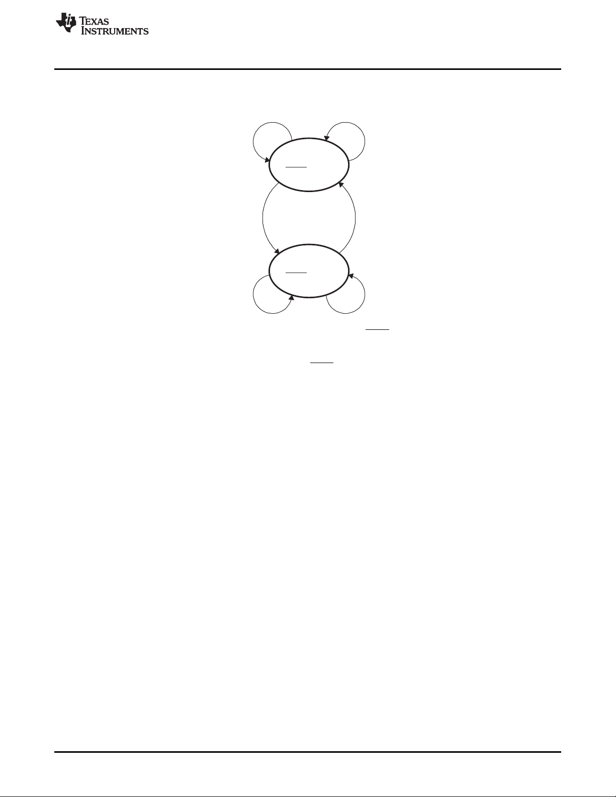
5 Interrupts Between the Host and the CPU
The host can interrupt the CPU of the DSP via the DSPINT bit of the HPIC, as described in Section 5.1.
The CPU can send an interrupt to the host by using the HINT bit of HPIC, as described in Section 5.2.
5.1 DSPINT Bit: Host-to-CPU Interrupts
The DSPINT bit of HPIC allows the host to send an interrupt request to the CPU, as summarized in
Figure 26 and detailed following the figure.
Figure 26. Host-to-CPU Interrupt State Diagram
www.ti.com
5.2 HINT Bit: CPU-to-Host Interrupts
A When the DSPINT bit transitions from 0 to 1, an interrupt is generated to the CPU. No new interrupt can be generated
until the CPU has cleared the bit (DSPINT = 0).
To interrupt the CPU, the host must:
1. Drive both HCNTL1 and HCNTL0 low to request a write to HPIC.
2. Write 1 to the DSPINT bit in HPIC.
When the host sets the DSPINT bit, the HPI generates an interrupt pulse to the CPU that sets the
corresponding flag bit in an interrupt flag register of the CPU. If this maskable interrupt is properly enabled
in the CPU, the CPU executes the corresponding interrupt service routine (ISR). Before the host can use
DSPINT to generate a subsequent interrupt to the CPU, the CPU must acknowledge the current interrupt
by writing a 1 to the DSPINT bit. When the CPU writes 1, DSPINT is forced to 0. The host should verify
that DSPINT = 0 before generating subsequent interrupts. While DSPINT = 1, host writes to the DSPINT
bit do not generate an interrupt pulse.
Writes of 0 have no effect on the DSPINT bit. A hardware reset immediately clears DSPINT and thus
clears an active host-to-CPU interrupt.
The HINT bit of HPIC allows the CPU to send an interrupt request to the host, as summarized in Figure 27
and detailed following the figure.
30
Host Port Interface (HPI) SPRUGK7A–March 2009–Revised July 2010
Copyright © 2009–2010, Texas Instruments Incorporated
Page 31
HINT bit=0
HINT
signal
is high
is low
HINT signal
HINT bit=1
CPU writes 1
to HINT bit
Host writes 1
to HINT bit
Interrupt
active
CPU writes 0
to HINT bit
No interrupt/
interrupt
cleared
Host writes 0 or 1
to HINT bit
CPU writes 0 or 1
to HINT bit
Host writes 0
to HINT bit
www.ti.com
If the CPU writes 1 to the HINT bit of HPIC, the HPI drives the HINT signal low, indicating an interrupt
condition to the host. Before the CPU can use the HINT bit to generate a subsequent interrupt to host, the
host must acknowledge the current interrupt by writing 1 to the HINT bit. When the host does this, the HPI
clears the HINT bit (HINT = 0), and this drives the HINT signal high. The CPU should read HPIC and
ensure HINT = 0 before generating subsequent interrupts. Writes of 0 have no effect on the HINT bit. A
hardware reset immediately clears the HINT bit and thus clears an active CPU-to-host interrupt.
Interrupts Between the Host and the CPU
Figure 27. CPU-to-Host Interrupt State Diagram
SPRUGK7A–March 2009–Revised July 2010 Host Port Interface (HPI)
Copyright © 2009–2010, Texas Instruments Incorporated
31
Page 32

Write FIFO
control logic
Host write
pointer
HPI DMA
read pointer
Write FIFO
Host
writes
Read FIFO
reads
Host
control logic
Read FIFO
Host read
pointer
HPI DMA
write pointer
HPI
DMA
logic
Switched
central
Burst
writes
reads
Burst
resource
DSP
internal/
external
memory
FIFOs and Bursting
6 FIFOs and Bursting
The HPI data register (HPID) is a port through which the host accesses two first-in, first-out buffers
(FIFOs). As shown in Figure 28, a read FIFO supports host read cycles, and a write FIFO supports host
write cycles. Both read and write FIFOs are 8-words deep (each word is 32 bits). If the host is performing
multiple reads or writes to consecutive memory addresses (autoincrement HPID cycles), the FIFOs are
used for bursting. The HPI DMA logic reads or writes a burst of four words at a time when accessing one
of the FIFOs.
Bursting is essentially invisible to the host because the host interface signaling is not affected. Its benefit
to the host is that the HRDY signal is deasserted less often when there are multiple reads or writes to
consecutive addresses.
www.ti.com
Figure 28. FIFOs in the HPI
6.1 Read Bursting
When the host writes to the read address register (HPIAR), the read FIFO is flushed. Any host read data
that was in the read FIFO is discarded (the read FIFO pointers are reset). If an HPI DMA write to the read
FIFO is in progress at the time of a flush request, the HPI allows this write to complete and then performs
the flush.
After any read FIFO flush, no read cycles are being initiated. Read bursting can begin in one of two ways:
the host initiates an HPID read cycle with autoincrementing, or the host initiates issues a FETCH
command (writes 1 to the FETCH bit in HPIC).
32
Host Port Interface (HPI) SPRUGK7A–March 2009–Revised July 2010
Copyright © 2009–2010, Texas Instruments Incorporated
Page 33

www.ti.com
If the host initiates an HPID read cycle with autoincrementing, the HPI DMA logic performs two 4-word
burst operations to fill the read FIFO. The host is initially held off by the deassertion of the HRDY signal
until data is available to be read from the read FIFO. Once data is available in the read FIFO, the host can
read data from the read FIFO by performing subsequent reads of HPID with autoincrementing. Once the
initial read has been performed, the HPI DMA logic continues to perform 4-word burst operations to
consecutive memory addresses every time there are four empty word locations in the read FIFO. The HPI
DMA logic continues to prefetch data to keep the read FIFO full, until the occurrence of an event that
causes a read FIFO flush (see Section 6.3).
As mentioned, read bursting may also begin with a FETCH command. The host should always precede
the FETCH command with the initialization of the HPIAR register or a non-autoincrement access, so that
the read FIFO is flushed beforehand. When the host initiates a FETCH command, the HPI DMA logic
begins to prefetch data to keep the read FIFO full, as described in the previous paragraph. The FETCH bit
in HPIC does not actually store the value that is written to it; rather, the decoding of a host write of 1 to
this bit is considered a FETCH command.
The FETCH command can be helpful if the host does not use the HRDY signal. The host can initiate
prefetching by writing 1 to the FETCH bit and then poll the HRDY bit, which is also in HPIC. When the
HRDY bit is 1, the host can perform an HPID read cycle. See Section 4 for more details on the HRDY bit.
Both types of continuous or burst reads described previously begin with a write to the HPI address
register, which causes a read FIFO flush. This is the typical way of initiating read cycles, because the
initial read address needs to be specified.
An HPID read cycle without autoincrementing does not initiate any prefetching activity. Instead, it causes
the read FIFO to be flushed and causes the HPI DMA logic to perform a single-word read from the
processor memory. As soon as the host activates a read cycle without autoincrementing, prefetching
activity ceases until the occurrence of a FETCH command or an autoincrement read cycle. A
non-autoincrement read cycle always should be preceded by another non-autoincrement cycle or the
direct initialization of HPIAR, so that the read FIFO is flushed beforehand.
FIFOs and Bursting
6.2 Write Bursting
A write to the write address register (HPIAW) causes the write FIFO to be flushed. This means that any
write data in the write FIFO is forced to its destination in the processor memory (the HPI DMA logic
performs burst operations until the write FIFO is empty). When the FIFO has been flushed, the only action
that will cause the HPI DMA logic to perform burst writes is a host write to HPID with autoincrementing.
The initial host-write data is stored in the write FIFO. An HPI DMA write is not requested until there are
four words in the write FIFO. As soon as four words have been written to the FIFO via the HPID write
cycles with autoincrementing, the HPI DMA logic performs a 4-word burst operation to the processor
memory. The burst operations continue as long as there are at least four words in the FIFO. If the FIFO
becomes full (eight words are waiting in the FIFO), the HPI holds off the host by deasserting HRDY until at
least one empty word location is available in the FIFO.
Because excessive time might pass between consecutive burst operations, the HPI has a time-out
counter. If there are fewer than four words in the write FIFO and the time-out counter expires, the HPI
DMA logic empties the FIFO immediately by performing a 2-word or 3-word burst, or a single-word write,
as necessary. Every time new data is written to the write FIFO, the time-out counter is automatically reset
to begin its count again. The time-out period is 256 internal clock cycles. See the device-specific data
manual to determine how the HPI is clocked on your device.
An HPID write cycle without autoincrementing does not initiate any bursting activity. Instead, it causes the
write FIFO to be flushed and causes the HPI DMA logic to perform a single-word write to the processor
memory. As soon as the host activates a write cycle without autoincrementing, bursting activity ceases
until the occurrence of an autoincrement write cycle. A non-autoincrement write cycle always should be
preceded by the initialization of HPIAW or by another non-autoincrement access, so that the write FIFO is
flushed beforehand.
SPRUGK7A–March 2009–Revised July 2010 Host Port Interface (HPI)
Copyright © 2009–2010, Texas Instruments Incorporated
33
Page 34

FIFOs and Bursting
6.3 FIFO Flush Conditions
When specific conditions occur within the HPI, the read or write FIFO must be flushed to prevent the
reading of stale data from the FIFOs. When a read FIFO flush condition occurs, all current host accesses
and direct memory accesses (DMAs) to the read FIFO are allowed to complete. This includes DMAs that
have been requested but not yet initiated. The read FIFO pointers are then reset, causing any read data to
be discarded.
Similarly, when a write FIFO flush condition occurs, all current host accesses and DMAs to the write FIFO
are allowed to complete. This includes DMAs that have been requested but not yet initiated. All posted
writes in the FIFO are then forced to completion with a final burst or single-word write, as necessary.
If the host initiates an HPID host cycle during a FIFO flush, the cycle is held off with the deassertion of
HRDY until the flush is complete and the FIFO is ready to be accessed.
The following conditions cause the read and write FIFOs to be flushed:
• Read FIFO flush conditions:
– A value from the host is written to the read address register (HPIAR)
– The host performs an HPID read cycle without autoincrementing
• Write FIFO flush conditions:
– A value from the host is written to the write address register (HPIAW)
– The host performs an HPID write cycle without autoincrementing
– The write-burst time-out counter expires
When operating with DUALHPIA = 0 (all HPIA writes and increments affect both HPIAR and HPIAW), any
read or write flush condition causes both read and write FIFOs to be flushed. In addition, the following
scenarios cause both FIFOs to be flushed when DUALHPIA = 0:
• The host performs an HPID write cycle with autoincrementing while the read FIFO is not empty (the
read FIFO still contains data from prefetching or an HPID read cycle with autoincrementing).
• The host performs an HPID read cycle with autoincrementing while the write FIFO is not empty (there
is still posted write data in the write FIFO).
This is useful in providing protection against reading stale data by reading a memory address when a
previous write cycle has not been completed at the same address. Similarly, this protects against
overwriting data at a memory address when a previous read cycle has not been completed at the same
address.
When operating with DUALHPIA = 1 (HPIAR and HPIAW are independent), there is no such protection.
However, when DUALHPIA = 1, data flow can occur in both directions without flushing both FIFOs
simultaneously, thereby improving HPI bandwidth.
www.ti.com
6.4 FIFO Behavior When a Hardware Reset or Software Reset Occurs
A hardware reset (device-level reset) or an HPI software reset (HPIRST = 1 in HPIC) causes the FIFOs to
be reset. The FIFO pointers are cleared, so that all data in the FIFOs are discarded. In addition, all
associated FIFO logic is reset.
If a host cycle is active when a hardware or HPI software reset occurs, the HRDY signal is asserted
(driven low), allowing the host to complete the cycle. When the cycle is complete, HRDY is deasserted
(driven high). Any access interrupted by a reset may result in corrupted read data or a lost write data (if
the write does not actually update the intended memory or register). Although data may be lost, the host
interface protocol is not violated. While either of reset condition is true, and the host is idle (internal
HSTRB is held high), the FIFOs are held in reset, and host transactions are held off with an inactive
HRDY signal.
34
Host Port Interface (HPI) SPRUGK7A–March 2009–Revised July 2010
Copyright © 2009–2010, Texas Instruments Incorporated
Page 35

www.ti.com
7 Emulation and Reset Considerations
7.1 Emulation Modes
The FREE and SOFT bits of the power and emulation management register (PWREMU_MGMT)
determine the response of the HPI to an emulation suspend condition. If FREE = 1, the HPI is not
affected, and the SOFT bit has no effect. If FREE = 0 and SOFT = 0, the HPI is not affected. If FREE = 0
and SOFT = 1:
• The HPI DMA logic halts after the current host and HPI DMA operations are completed.
• The external host interface functions as normal throughout the emulation suspend condition. The host
may access the control register (HPIC). In the 16-bit and 32-bit multiplexed modes, the host may also
access the HPIA registers and may perform data reads until the read FIFO is empty or data writes until
the write FIFO is full. As in normal operation, the HRDY pin is driven high during a host cycle that
cannot be completed due to the write FIFO being full or the read FIFO being empty. If this occurs,
HRDY continues to be driven high, holding off the host, until the emulation suspend condition is over
and the FIFOs are serviced by the HPI DMA logic, allowing the host cycle to complete.
• When the emulation suspend condition is over, the appropriate requests by the HPI DMA logic are
made to process any posted host writes in the write FIFO or to fill the read FIFO as necessary. HPI
operation then continues as normal.
7.2 Software Reset Considerations
The control register (HPIC) provides an HPI software reset bit (HPIRST) that is used to reset the read and
write FIFOs. When the CPU sets the HPIRST bit:
• If the internal strobe signal, internal HSTRB, is high (host is inactive), HRDY is driven high and remains
high until the reset condition is over.
• If internal HSTRB is low (host cycle is active), direct memory accesses (DMAs) of the FIFOs are
allowed to complete. Then HRDY is driven low, allowing the host to complete the cycle. When internal
HSTRB goes high (cycle is complete), HRDY is driven high and remains high until the reset condition
is over. If the active cycle was a write cycle, the memory or register may not have been correctly
updated. If the active cycle was a read cycle, the fetched value may not be valid.
• After any remaining DMAs of the FIFOs are complete, the read and write FIFOs and the associated
FIFO logic are reset. The FIFO pointers are cleared, so that any data in the FIFOs are discarded. The
CPU reads 0 in HPIRST until the FIFOs are fully reset. Writing 0 to HPIRST before the FIFO reset is
complete will not stop the FIFO reset from occurring.
An HPI software reset does not reset any HPI registers other than the FIFOs.
Emulation and Reset Considerations
7.3 Hardware Reset Considerations
When the DSP is reset:
• If the internal strobe signal, internal HSTRB, is high (host is inactive), HRDY is driven high and remains
high until the reset condition is over.
• If internal HSTRB is low (host cycle is active), HRDY is driven low, allowing the host to complete the
cycle. When internal HSTRB goes high (cycle is complete), HRDY is driven high and remains high until
the reset condition is over. If the active cycle was a write cycle, the memory or register may not have
been correctly updated. If the active cycle was a read cycle, the fetched value may not be valid.
• The HPI registers are reset to their default values. These default values are shown under each bit field
of the register figures in Section 8.
• The read and write FIFOs and the associated FIFO logic are reset (this includes a flush of the FIFOs).
• Host-to-CPU and CPU-to-host interrupts are cleared.
SPRUGK7A–March 2009–Revised July 2010 Host Port Interface (HPI)
Copyright © 2009–2010, Texas Instruments Incorporated
35
Page 36

HPI Registers
8 HPI Registers
8.1 Introduction
Table 6 lists the memory-mapped registers for the Host Port Interface (HPI). See the device-specific data
manual for the memory address of these registers.
Offset Acronym Register Description See
0004h PWREMU_MGMT Power and Emulation Management Register Section 8.2
0030h HPIC Host Port Interface Control Register Section 8.3
0034h HPIAW Host Port Interface Address Register (Write) Section 8.4
0038h HPIAR Host Port Interface Address Register (Read) Section 8.4
None HPID Data Register Section 8.5
www.ti.com
Table 6. Host Port Interface (HPI) Registers
36
Host Port Interface (HPI) SPRUGK7A–March 2009–Revised July 2010
Copyright © 2009–2010, Texas Instruments Incorporated
Page 37

www.ti.com
HPI Registers
8.2 Power and Emulation Management Register (PWREMU_MGMT)
The power management and emulation register is shown in Figure 29 and described in Table 7.
Figure 29. Power and Emulation Management Register (PWREMU_MGMT)
31-16
Reserved
R-0
15-2 1 0
Reserved SOFT FREE
R-0 R/W-0 R/W-0
LEGEND: R/W = Read/Write; R = Read only; -n = value after reset
Table 7. Power and Emulation Management Register (PWREMU_MGMT) Field Descriptions
Bit Field Value Description
31-2 Reserved Reserved
1 SOFT Determines emulation mode functionality of the HPI. When the FREE bit is cleared, the SOFT bit
0 FREE Free run emulation control. Determines emulation mode functionality of the HPI. When the FREE
selects the HPI mode.
0 Upon emulation suspend, the HPI operation is not affected.
1 In response to an emulation suspend event, the HPI logic halts after the current HPI transaction is
completed.
bit is cleared, the SOFT bit selects the HPI mode.
0 The SOFT bit selects the HPI mode.
1 The HPI runs free regardless of the SOFT bit.
SPRUGK7A–March 2009–Revised July 2010 Host Port Interface (HPI)
Copyright © 2009–2010, Texas Instruments Incorporated
37
Page 38

HPI Registers
www.ti.com
8.3 Host Port Interface Control Register (HPIC)
The HPIC register stores control and status bits used to configure and operate the HPI peripheral. The bit
positions of the HPIC register and their functions are illustrated in Table 8.
In 16-bit multiplexed mode, the lower 16 bits of the HPIC register are duplicated on the upper 16 bits
during host accesses. Therefore, reading the upper or lower halfword of the HPIC register returns the
same value.
As shown in Figure 30 and Figure 31, the host and the CPU do not have the same access permissions.
The host owns HPIC and thus has full read/write access. The CPU has primarily read-only access, but the
exceptions are:
• The CPU can write 1 to the HINT bit to generate an interrupt to the host.
• The CPU can write 1 to the DSPINT bit to clear/acknowledge an interrupt from the host.
The host port interface control register is shown in Figure 30 and Figure 31 and described in Table 8.
Figure 30. Host Access Permissions
31 16
Reserved
R-0
15 12 11 10 9 8
Reserved HPIARWSEL Reserved DUALHPIA HWOBSTAT
R-0 R/W-0 R-0 R/W-0 R-0
7 6 5 4 3 2 1 0
HPIRST Reserved
R-0 R/W-0 R/W-0 R-1 R/W1C-0 R/W-0 R/W-0
LEGEND: R/W = Read/Write; R = Read only; W1C = Write 1 to clear (writing 0 has no effect); -n = value after reset
A. Always keep this bit as zero.
(A)
FETCH HRDY HINT DSPINT HWOB
Figure 31. CPU Access Permissions
31 16
Reserved
R-0
15 12 11 10 9 8
Reserved HPIARWSEL Reserved DUALHPIA HWOBSTAT
R-0 R-0 R-0 R-0 R-0
7 6 5 4 3 2 1 0
(A)
HPIRST
R/W-0 or 1 R-0 R-0 R-0 R/W-0 R/W-0 R-0
LEGEND: R/W = Read/Write; R = Read only; -n = value after reset
A. This bit defaults to 0 when HPI boot is selected; otherwise it defaults to 1.
Reserved FETCH HRDY HINT DSPINT HWOB
Table 8. Host Port Interface Control Register (HPIC) Field Descriptions
Bit Field Value Description
31-12 Reserved 0 Read-only reserved bits. Reads return 0.
11 HPIARWSEL HPIA read/write select bit (configured by the host). This bit is applicable only in the dual-HPIA mode
10 Reserved 0 Read-only reserved bits. Reads return 0.
(DUALHPIA = 1).
Note: HPIARWSEL does not affect the HPI DMA logic. Regardless of the value of HPIARWSEL,
the HPI DMA logic uses HPIAW when writing to memory and HPIAR when reading from memory..
0 In the next HPIA host cycle, the host will access HPIAW (the write address register).
1 In the next HPIA host cycle, the host will access HPIAR (the read address register).
38
Host Port Interface (HPI) SPRUGK7A–March 2009–Revised July 2010
Copyright © 2009–2010, Texas Instruments Incorporated
Page 39

www.ti.com
Table 8. Host Port Interface Control Register (HPIC) Field Descriptions (continued)
Bit Field Value Description
9 DUALHPIA Dual-HPIA mode bit (configured by the host).
0 Single-HPIA mode. From the host's perspective, there is one 32-bit HPIA register. A host HPIA
write cycle places the same value in both HPIAR and HPIAW. During autoincrementing, both
HPIAR and HPIAW are incremented. A host HPIA read cycle retrieves the value from HPIAR.
1 Dual-HPIA mode. The host sees two 32-bit HPIA registers: HPIAR for read addresses and HPIAW
for write addresses.
8 HWOBSTAT HWOB status bit. HWOBSTAT reflects the value of the HWOB bit (see bit 0).
0 HWOB bit = 0 (first halfword is most significant)
1 HWOB bit = 1 (first halfword is least significant)
7 HPIRST HPI software reset bit (set by CPU).
0 Host: Reads of HPIRST always return 0.
CPU: Once the CPU has written 1 to HPIRST, reads return 0 until the FIFOs are completely reset.
Writing 0 before the reset process is complete will not stop the reset from occurring.
1 CPU: Writing 1 causes the read and write FIFOs and the associated FIFO logic to be reset. As
described in Section 7.2, an active host cycle is allowed to complete before the reset process
begins. When HPIRST = 1, the HRDY pin is deasserted (not ready), thereby holding off all host
accesses. The CPU must set HPIRST = 0 to allow host accesses.
6-5 Reserved 0 The host must write 0s to these bits. The CPU cannot modify these bits.
4 FETCH Host data fetch command bit (set by host).
0 CPU/Host: Reads of FETCH always return 0.
1 Host: Write 1 to tell the HPI DMA logic to pre-fetch data into the read FIFO.
3 HRDY HPI-ready indicator (read-only).
0 Host: Internal HRDY is low. The HPI is not ready to complete a host cycle.
CPU: Reads of HRDY always return 0.
1 Host: Internal HRDY is high. The HPI is ready to complete a host cycle.
Note: HRDY bit is not the same as the HRDY pin status. Refer to Section 4 for details.
2 HINT Host interrupt bit (set by the CPU, cleared by the host).
0 CPU/Host: Writing 0 has no effect.
1 CPU: Writing 1 to HINT generates a CPU-to-host interrupt. HINT remains 1 until it is cleared by the
host or by a hardware reset.
Host: Writing 1 to HINT clears HINT to 0, to acknowledge the CPU-to-host interrupt.
1 DSPINT DSP interrupt bit (set by the host, cleared by the CPU).
0 CPU/Host: Writing 0 has no effect.
1 CPU: Writing 1 to DSPINT clears DSPINT to 0, to acknowledge the host-to-CPU interrupt.
Host: Writing 1 to DSPINT generates a host-to-CPU interrupt. DSPINT remains 1 until it is cleared
by the CPU or by a hardware reset.
0 HWOB Halfword order bit (configured by the host). This bit is applicable only in the 16-bit multiplexed
mode. HWOB must be initialized by the host before the first data or address register access. The
status of HWOB is also reflected in HWOBSTAT (see bit 8).
For host write cycle:
0 The first halfword received from the bus is most significant (written to the high half of
HPID/HPIC/HPIAR/HPIAW). The second halfword is least significant (written to the low half of
HPID/HPIC/HPIAR/HPIAW).
1 The first halfword received from the bus is least significant (written to the low half of
HPID/HPIC/HPIAR/HPIAW). The second halfword is most significant (written to the high half of
HPID/HPIC/HPIAR/HPIAW).
For host read cycle:
0 The first halfword transmitted on the bus is most significant (taken from the high half of
HPID/HPIC/HPIAR/HPIAW). The second halfword is least significant (taken from the low half of
HPID/HPIC/HPIAR/HPIAW).
1 The first halfword transmitted on the bus is least significant (taken from the low half of
HPID/HPIC/HPIAR/HPIAW). The second halfword is most significant (taken from the high half of
HPID/HPIC/HPIAR/HPIAW).
HPI Registers
SPRUGK7A–March 2009–Revised July 2010 Host Port Interface (HPI)
Copyright © 2009–2010, Texas Instruments Incorporated
39
Page 40

HPI Registers
8.4 Host Port Interface Address Registers (HPIAW and HPIAR)
There are two 32-bit HPIA registers: HPIAW for write operations and HPIAR for read operations. The HPI
can be configured such that HPIAW and HPIAR act as a single 32-bit HPIA (single-HPIA mode) or as two
separate 32-bit HPIAs (dual-HPIA mode) from the perspective of the host. For details about these HPIA
modes, see Section 2.
Figure 32 and Figure 33 show the format of an address register during host and CPU accesses. As shown
in the figures, the host has full read/write access to the HPIAs, while the CPU can only read the HPIAs.
CAUTION
The host must always write a word address to the HPIAs. For example, L2
memory has a base byte address of 80 0000h that corresponds to a word
address of 20 0000h. A host must write 20 0000h to the HPIA register to point
the HPI to the base of L2 memory.
Figure 32. Format of an Address Register (HPIAW or HPIAR) - Host Access Permissions
31-0
ADDRESS
R/W-0
LEGEND: R = Read only; W = Write; -n = value after reset
www.ti.com
Figure 33. Format of an Address Register (HPIAW or HPIAR) - CPU Access Permissions
31-0
ADDRESS
R-0
LEGEND: R = Read only; -n = value after reset
Table 9. Host Port Interface Address Registers (HPIAW or HPIAR) Field Descriptions
Bit Field Value Description
31-0 ADDRESS Read/write address. The host must initiate this field with a word address.
40
Host Port Interface (HPI) SPRUGK7A–March 2009–Revised July 2010
Copyright © 2009–2010, Texas Instruments Incorporated
Page 41

www.ti.com
8.5 Data Register (HPID)
The 32-bit register HPID provides the data path between the host and the HPI DMA logic. During a host
write cycle, the host fills HPID with 32 bits, and then the HPI DMA logic transfers the 32-bit value to the
internal memory of the DSP. During a host read cycle, the HPI DMA logic fills HPID with 32 bits from the
internal memory, and then the HPI transfers the 32-bit value to the host. A host cycle is a single 32-bit
transfer (in the 32-bit multiplexed mode) or two consecutive 16-bit transfers (in the 16-bit multiplexed
mode).
As shown in Figure 34, the host has full read/write access to HPID. The CPU cannot access HPID.
In the multiplexed modes, HPID is actually a port through which the host accesses two first-in, first-out
buffers (FIFOs). The read FIFO and the write FIFO play a significant role in providing a higher data
throughput. For information about the FIFOs, see Section 6.
Figure 34. Data Register (HPID) (Host access permissions, CPU cannot access HPID)
LEGEND: R = Read only; W = Write; -n = Value after hardware reset
Table 10. Data Register (HPID) Field Descriptions
Bit Field Value Description
31-0 DATA HPI data
HPI Registers
31-0
DATA
R/W-0
SPRUGK7A–March 2009–Revised July 2010 Host Port Interface (HPI)
Copyright © 2009–2010, Texas Instruments Incorporated
41
Page 42

Appendix A Revision History
This revision history highlights the technical changes made to the document in this revision.
See Additions/Modifications/Deletions
Table 6 Modified table
www.ti.com
Table 11. TMS320C6457 HPI Revision History
42
Revision History SPRUGK7A–March 2009–Revised July 2010
Copyright © 2009–2010, Texas Instruments Incorporated
Page 43

IMPORTANT NOTICE
Texas Instruments Incorporated and its subsidiaries (TI) reserve the right to make corrections, modifications, enhancements, improvements,
and other changes to its products and services at any time and to discontinue any product or service without notice. Customers should
obtain the latest relevant information before placing orders and should verify that such information is current and complete. All products are
sold subject to TI’s terms and conditions of sale supplied at the time of order acknowledgment.
TI warrants performance of its hardware products to the specifications applicable at the time of sale in accordance with TI’s standard
warranty. Testing and other quality control techniques are used to the extent TI deems necessary to support this warranty. Except where
mandated by government requirements, testing of all parameters of each product is not necessarily performed.
TI assumes no liability for applications assistance or customer product design. Customers are responsible for their products and
applications using TI components. To minimize the risks associated with customer products and applications, customers should provide
adequate design and operating safeguards.
TI does not warrant or represent that any license, either express or implied, is granted under any TI patent right, copyright, mask work right,
or other TI intellectual property right relating to any combination, machine, or process in which TI products or services are used. Information
published by TI regarding third-party products or services does not constitute a license from TI to use such products or services or a
warranty or endorsement thereof. Use of such information may require a license from a third party under the patents or other intellectual
property of the third party, or a license from TI under the patents or other intellectual property of TI.
Reproduction of TI information in TI data books or data sheets is permissible only if reproduction is without alteration and is accompanied
by all associated warranties, conditions, limitations, and notices. Reproduction of this information with alteration is an unfair and deceptive
business practice. TI is not responsible or liable for such altered documentation. Information of third parties may be subject to additional
restrictions.
Resale of TI products or services with statements different from or beyond the parameters stated by TI for that product or service voids all
express and any implied warranties for the associated TI product or service and is an unfair and deceptive business practice. TI is not
responsible or liable for any such statements.
TI products are not authorized for use in safety-critical applications (such as life support) where a failure of the TI product would reasonably
be expected to cause severe personal injury or death, unless officers of the parties have executed an agreement specifically governing
such use. Buyers represent that they have all necessary expertise in the safety and regulatory ramifications of their applications, and
acknowledge and agree that they are solely responsible for all legal, regulatory and safety-related requirements concerning their products
and any use of TI products in such safety-critical applications, notwithstanding any applications-related information or support that may be
provided by TI. Further, Buyers must fully indemnify TI and its representatives against any damages arising out of the use of TI products in
such safety-critical applications.
TI products are neither designed nor intended for use in military/aerospace applications or environments unless the TI products are
specifically designated by TI as military-grade or "enhanced plastic." Only products designated by TI as military-grade meet military
specifications. Buyers acknowledge and agree that any such use of TI products which TI has not designated as military-grade is solely at
the Buyer's risk, and that they are solely responsible for compliance with all legal and regulatory requirements in connection with such use.
TI products are neither designed nor intended for use in automotive applications or environments unless the specific TI products are
designated by TI as compliant with ISO/TS 16949 requirements. Buyers acknowledge and agree that, if they use any non-designated
products in automotive applications, TI will not be responsible for any failure to meet such requirements.
Following are URLs where you can obtain information on other Texas Instruments products and application solutions:
Products Applications
Amplifiers amplifier.ti.com Audio www.ti.com/audio
Data Converters dataconverter.ti.com Automotive www.ti.com/automotive
DLP® Products www.dlp.com Communications and www.ti.com/communications
DSP dsp.ti.com Computers and www.ti.com/computers
Clocks and Timers www.ti.com/clocks Consumer Electronics www.ti.com/consumer-apps
Interface interface.ti.com Energy www.ti.com/energy
Logic logic.ti.com Industrial www.ti.com/industrial
Power Mgmt power.ti.com Medical www.ti.com/medical
Microcontrollers microcontroller.ti.com Security www.ti.com/security
RFID www.ti-rfid.com Space, Avionics & www.ti.com/space-avionics-defense
RF/IF and ZigBee® Solutions www.ti.com/lprf Video and Imaging www.ti.com/video
Mailing Address: Texas Instruments, Post Office Box 655303, Dallas, Texas 75265
Copyright © 2010, Texas Instruments Incorporated
Telecom
Peripherals
Defense
Wireless www.ti.com/wireless-apps
 Loading...