

Page 1

TMS320C5514
www.ti.com
TMS320C5514 Fixed-Point Digital Signal Processor
Check for Samples: TMS320C5514
1 Fixed-Point Digital Signal Processor
1.1 Features
12
• HIGHLIGHTS:
• High-Perf/Low-Power, C55x™ Fixed-Point DSP
– 16.67/13.33/10/8.33-ns Instruction Cycle Time
– 60-, 75-, 100-, 120-MHz Clock Rate
• 256K Bytes On-Chip RAM
• 16-/8-Bit External Memory Interface (EMIF)
• Two MultiMedia Card/Secure Digital I/Fs
• Serial-Port I/F (SPI) With Four Chip-Selects
• Four Inter-IC Sound (I2S Bus™)
• USB 2.0 Full- and High-Speed Device
• Real-Time Clock (RTC) With Crystal Input
• Four Core Isolated Power Supply Domains
• Four I/O Isolated Power Supply Domains
• Three Integrated LDOs
• Industrial Temperature Devices Available
• 1.05-V Core, 1.8/2.5/2.75/3.3-V I/Os
• 1.3-V Core, 1.8/2.5/2.75/3.3-V I/Os
• FEATURES:
• High-Performance, Low-Power, TMS320C55x™
Fixed-Point Digital Signal Processor
– 16.67-, 13.33-, 10-, 8.33-ns Instruction Cycle
Time
– 60-, 75-, 100-, 120-MHz Clock Rate
– One/Two Instruction(s) Executed per Cycle
– Dual Multipliers [Up to 200 or 240 Million
Multiply-Accumulates per Second (MMACS)]
– Two Arithmetic/Logic Units (ALUs)
– Three Internal Data/Operand Read Buses
and Two Internal Data/Operand Write Buses
– Software-Compatible With C55x Devices
SPRS646B–AUGUST 2010–REVISED AUGUST 2010
– Industrial Temperature Devices Available
• 256K Bytes Zero-Wait State On-Chip RAM,
Composed of:
– 64K Bytes of Dual-Access RAM (DARAM),
8 Blocks of 4K x 16-Bit
– 192K Bytes of Single-Access RAM (SARAM),
24 Blocks of 4K x 16-Bit
• 128K Bytes of Zero Wait-State On-Chip ROM
(4 Blocks of 16K x 16-Bit)
• 4M x 16-Bit Maximum Addressable External
Memory Space (SDRAM/mSDRAM)
• 16-/8-Bit External Memory Interface (EMIF) with
Glueless Interface to:
– 8-/16-Bit NAND Flash, 1- and 4-Bit ECC
– 8-/16-Bit NOR Flash
– Asynchronous Static RAM (SRAM)
– SDRAM/mSDRAM (1.8-, 2.5-, 2.75-, and 3.3-V)
• Direct Memory Access (DMA) Controller
– Four DMA With 4 Channels Each
(16-Channels Total)
• Three 32-Bit General-Purpose Timers
– One Selectable as a Watchdog and/or GP
• Two MultiMedia Card/Secure Digital (MMC/SD)
Interfaces
• Universal Asynchronous Receiver/Transmitter
(UART)
• Serial-Port Interface (SPI) With Four
Chip-Selects
• Master/Slave Inter-Integrated Circuit (I2C Bus™)
• Four Inter-IC Sound (I2S Bus™) for Data
Transport
1
Please be aware that an important notice concerning availability, standard warranty, and use in critical applications of Texas
Instruments semiconductor products and disclaimers thereto appears at the end of this data sheet.
2All trademarks are the property of their respective owners.
PRODUCTION DATA information is current as of publication date.
Products conform to specifications per the terms of the Texas
Instruments standard warranty. Production processing does not
necessarily include testingof all parameters.
Copyright © 2010, Texas Instruments Incorporated
Page 2

TMS320C5514
SPRS646B–AUGUST 2010–REVISED AUGUST 2010
www.ti.com
• Device USB Port With Integrated 2.0 • Up to 26 General-Purpose I/O (GPIO) Pins
High-Speed PHY that Supports: (Multiplexed With Other Device Functions)
– USB 2.0 Full- and High-Speed Device • 196-Terminal Pb-Free Plastic BGA (Ball Grid
• Real-Time Clock (RTC) With Crystal Input, With
Array) (ZCH Suffix)
Separate Clock Domain, Separate Power • 1.05-V Core (60 or 75 MHz), 1.8-V, 2.5-V, 2.75-V,
Supply or 3.3-V I/Os
• Four Core Isolated Power Supply Domains: • 1.3-V Core (100, 120 MHz), 1.8-V, 2.5-V, 2.75-V,
Analog, RTC, CPU and Peripherals, and USB or 3.3-V I/Os
• Four I/O Isolated Power Supply Domains: RTC • Applications:
I/O, EMIF I/O, USB PHY, and DV
DDIO
– Wireless Audio Devices (e.g., Headsets,
• Three integrated LDOs (DSP_LDO, ANA_LDO, Microphones, Speakerphones, etc.)
and USB_LDO) to power the isolated domains:
DSP Core, Analog, and USB Core, respectively
• Low-Power S/W Programmable Phase-Locked
Loop (PLL) Clock Generator
• On-Chip ROM Bootloader (RBL) to Boot From
NAND Flash, NOR Flash, SPI EEPROM, SPI
Serial Flash or I2C EEPROM
• IEEE-1149.1 (JTAG™)
Boundary-Scan-Compatible
– Echo Cancellation Headphones
– Portable Medical Devices
– Voice Applications
– Industrial Controls
– Fingerprint Biometrics
– Software Defined Radio
• Community Resources
– TI E2E Community
– TI Embedded Processors Wiki
2 Fixed-Point Digital Signal Processor Copyright © 2010, Texas Instruments Incorporated
Submit Documentation Feedback
Product Folder Link(s): TMS320C5514
Page 3

TMS320C5514
www.ti.com
1.2 Description
The device is a member of TI's TMS320C5000™ fixed-point Digital Signal Processor (DSP) product family
and is designed for low-power applications.
The fixed-point DSP is based on the TMS320C55x™ DSP generation CPU processor core. The C55x™
DSP architecture achieves high performance and low power through increased parallelism and total focus
on power savings. The CPU supports an internal bus structure that is composed of one program bus, one
32-bit data read bus and two 16-bit data read buses, two 16-bit data write buses, and additional buses
dedicated to peripheral and DMA activity. These buses provide the ability to perform up to four 16-bit data
reads and two 16-bit data writes in a single cycle. The device also includes four DMA controllers, each
with 4 channels, providing data movement for 16-independent channel contexts without CPU intervention.
Each DMA controller can perform one 32-bit data transfer per cycle, in parallel and independent of the
CPU activity.
The C55x CPU provides two multiply-accumulate (MAC) units, each capable of 17-bit x 17-bit
multiplication and a 32-bit add in a single cycle. A central 40-bit arithmetic/logic unit (ALU) is supported by
an additional 16-bit ALU. Use of the ALUs is under instruction set control, providing the ability to optimize
parallel activity and power consumption. These resources are managed in the Address Unit (AU) and Data
Unit (DU) of the C55x CPU.
The C55x CPU supports a variable byte width instruction set for improved code density. The Instruction
Unit (IU) performs 32-bit program fetches from internal or external memory and queues instructions for the
Program Unit (PU). The Program Unit decodes the instructions, directs tasks to the Address Unit (AU) and
Data Unit (DU) resources, and manages the fully protected pipeline. Predictive branching capability avoids
pipeline flushes on execution of conditional instructions.
SPRS646B–AUGUST 2010–REVISED AUGUST 2010
Serial media is supported through two MultiMedia Card/Secure Digital (MMC/SD) peripherals, four Inter-IC
Sound (I2S Bus™) modules, one Serial-Port Interface (SPI) with up to 4 chip selects, one I2C
multi-master and slave interface, and a Universal Asynchronous Receiver/Transmitter (UART) interface.
The device peripheral set includes an external memory interface (EMIF) that provides glueless access to
asynchronous memories like EPROM, NOR, NAND, and SRAM, as well as to high-speed, high-density
memories such as synchronous DRAM (SDRAM) and mobile SDRAM (mSDRAM). Additional peripherals
include: a high-speed Universal Serial Bus (USB2.0) device mode only, and a real-time clock (RTC). This
device also includes three general-purpose timers with one configurable as a watchdog timer, and an
analog phase-locked loop (APLL) clock generator.
Furthermore, the device includes three integrated LDOs (DSP_LDO, ANA_LDO, and USB_LDO) to power
different sections of the device. The DSP_LDO can provide 1.3 V or 1.05 V to the DSP core (CVDD). To
allow for lowest power operation, the programmer can shutdown the internal DSP_LDO cutting power to
the DSP core (CVDD) while an external supply provides power to the RTC (CV
ANA_LDO is designed to provide 1.3 V to the DSP PLL (V
(V
DDA_ANA
(USB_V
). The USB_LDO provides 1.3 V to USB core digital (USB_V
). The RTC alarm interrupt or the WAKEUP pin can re-enable the internal DSP_LDO and
DDA1P3
DDA_PLL
) and power management circuits
and DV
DDRTC
) and PHY circuits
DD1P3
DDRTC
). The
re-apply power to the DSP core.
The device is supported by the industry’s award-winning eXpressDSP™, Code Composer Studio™
Integrated Development Environment (IDE), DSP/BIOS™, Texas Instruments’ algorithm standard, and the
industry’s largest third-party network. Code Composer Studio IDE features code generation tools including
a C Compiler and Linker, RTDX™, XDS100™, XDS510™, XDS560™ emulation device drivers, and
evaluation modules. The device is also supported by the C55x DSP Library which features more than 50
foundational software kernels (FIR filters, IIR filters, and various math functions) as well as chip support
libraries.
Copyright © 2010, Texas Instruments Incorporated Fixed-Point Digital Signal Processor 3
Submit Documentation Feedback
Product Folder Link(s): TMS320C5514
Page 4
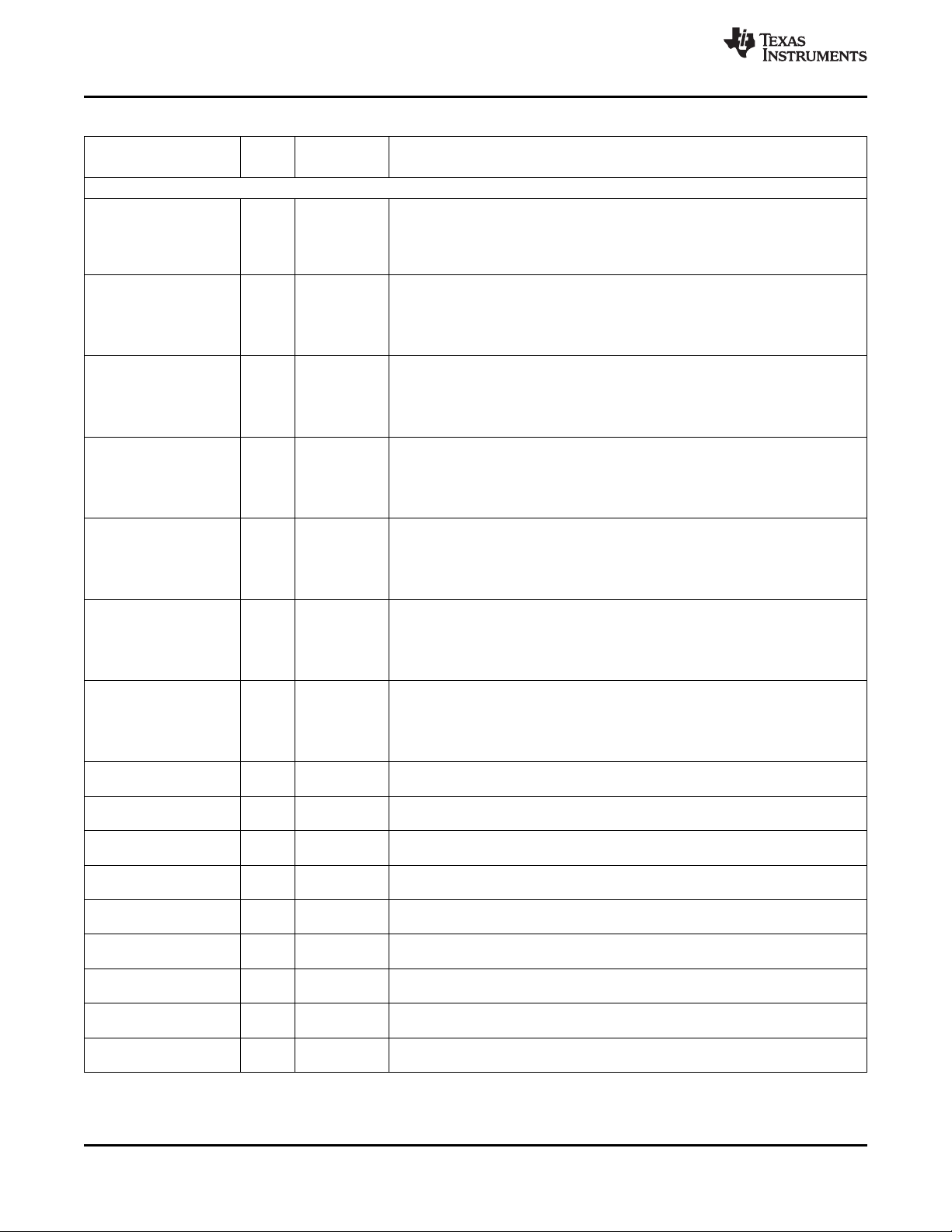
PLL/Clock
Generator
Power
Management
Pin
Multiplexing
JTAG Interface C55x™ DSP CPU
64 KB DARAM
192 KB SARAM
128 KB ROM
Switched Central Resource (SCR)
I S
(x4)
2
I C
2
SPI UART
Serial Interfaces
USB 2.0
PHY (HS)
[DEVICE]
Connectivity
Peripherals
Input
Clock(s)
DMA
(x4)
Interconnect
DSP System
System
NAND, NOR,
SRAM, mSDRAM
Program/Data Storage
MMC/SD
(x2)
GP Timer
(x2)
RTC
GP Timer
or WD
LDOs
TMS320C5514
SPRS646B–AUGUST 2010–REVISED AUGUST 2010
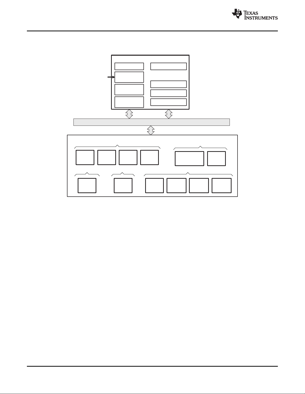
1.3 Functional Block Diagram
Figure 1-1 shows the functional block diagram of the device.
www.ti.com
Figure 1-1. Functional Block Diagram
4 Fixed-Point Digital Signal Processor Copyright © 2010, Texas Instruments Incorporated
Product Folder Link(s): TMS320C5514
Submit Documentation Feedback
Page 5

TMS320C5514
www.ti.com
1 Fixed-Point Digital Signal Processor ............... 1
1.1 Features .............................................. 1 6 Peripheral Information and Electrical
1.2 Description ........................................... 3
1.3 Functional Block Diagram ............................ 4
Specifications .......................................... 64
6.1 Parameter Information .............................. 64
6.2 Recommended Clock and Control Signal Transition
2 Revision History ......................................... 6
3 Device Overview ........................................ 7
3.1 Device Characteristics ............................... 7
3.2 C55x CPU ............................................ 9
3.3 Memory Map Summary ............................. 13
3.4 Pin Assignments .................................... 14
3.5 Terminal Functions ................................. 15
3.6 Device Support ..................................... 37
4 Device Configuration ................................. 40
4.1 System Registers ................................... 40
4.2 Power Considerations .............................. 41
4.3 Clock Considerations ............................... 45
4.4 Boot Sequence ..................................... 47
4.5 Configurations at Reset ............................ 50
4.6 Configurations After Reset ......................... 51
4.7 Multiplexed Pin Configurations ..................... 54
4.8 Debugging Considerations ......................... 58
5 Device Operating Conditions ....................... 60
5.1 Absolute Maximum Ratings Over Operating Case
Temperature Range (Unless Otherwise Noted) .... 60
5.2 Recommended Operating Conditions .............. 61
5.3 Electrical Characteristics Over Recommended
Ranges of Supply Voltage and Operating
6.3 Power Supplies ..................................... 65
6.4 External Clock Input From RTC_XI, CLKIN, and
6.5 Clock PLLs ......................................... 72
6.6 Direct Memory Access (DMA) Controller ........... 74
6.7 Reset ............................................... 75
6.8 Wake-up Events, Interrupts, and XF ............... 79
6.9 External Memory Interface (EMIF) ................. 81
6.10 Multimedia Card/Secure Digital (MMC/SD) ........ 95
6.11 Real-Time Clock (RTC) ........................... 100
6.12 Inter-Integrated Circuit (I2C) ...................... 103
6.13 Universal Asynchronous Receiver/Transmitter
6.14 Inter-IC Sound (I2S) ............................... 109
6.15 Serial Port Interface (SPI) ......................... 116
6.16 Universal Serial Bus (USB) 2.0 Controller ........ 119
6.17 General-Purpose Timers .......................... 126
6.18 General-Purpose Input/Output .................... 128
6.19 IEEE 1149.1 JTAG ................................ 132
7 Mechanical Packaging and Orderable
Information ............................................ 134
7.1 Thermal Data for ZCH ............................. 134
7.2 Packaging Information ............................ 134
SPRS646B–AUGUST 2010–REVISED AUGUST 2010
Temperature (Unless Otherwise Noted) ............ 62
Behavior ............................................ 64
USB_MXI Pins ...................................... 68
(UART) ............................................ 107
Copyright © 2010, Texas Instruments Incorporated Contents 5
Submit Documentation Feedback
Product Folder Link(s): TMS320C5514
Page 6
TMS320C5514
SPRS646B–AUGUST 2010–REVISED AUGUST 2010
www.ti.com
2 Revision History
This data manual revision history highlights the technical changes made to the SPRS646A device-specific
data manual to make it an SPRS646B revision.
Scope: Applicable updates to the TMS320C5000 device family, specifically relating to the TMS320C5514
device (Silicon Revisions 2.0) which is now in the production data (PD) stage of development have been
incorporated.
SEE ADDITIONS/MODIFICATIONS/DELETIONS
Section 1.1, Features
Section 3.1 Table 3-1, Characteristics of the C5514 Processor:
Device Characteristics
Section 3.5 Table 3-5, Oscillator/PLL Terminal Functions:
Terminal Functions
Section 4.2, Power Section 4.2.1.2, LDO Outputs:
Considerations
Section 5 Section 5.1, Absolute Maximum Ratings Over Operating Case Temperature Range (Unless Otherwise Noted):
Device Operating
Conditions
Section 6.3 Section 6.3.1, Power-Supply Sequencing:
Power Supplies
Section 6.4
External Clock Input From
RTC_XI, CLKIN, and
USB_MXI Pins:
Section 6.4.3 Figure 6-8, Connections when USB Oscillator is Permanently Disabled:
USB On-Chip Oscillator
With External Crystal
Section 6.5.1
PLL Device-Specific
Information
Section 6.9.2
EMIF Non-Mobile and
Mobile Synchronous DRAM
Memory Supported
Section 6.11
Real-Time Clock (RTC)
• Added 300 MMAC for Dual Multipliers
• Deleted Flash Cards row
• Updated Timers row
• Updated MMC/SD row
• Updated associated footnote
Table 3-17, Regulators and Power Management Terminal Functions:
• Updated LDOI description
Table 3-19, Supply Voltage Terminal Functions:
• Updated V
• Updated V
• Updated first paragraph
• Updated Device Operating Life Power-On Hours (POH) row
• Added footnote to Device Operating Life Power-On Hours (POH) row
Section 5.2, Recommended Operating Conditions:
• Added "For the device maximum..." footnote
Section 5.3, Electrical Characteristics Over Recommended Ranges of Supply Voltage and Operating
Temperature (Unless Otherwise Noted):
• Changed Analog PLL (V
• Deleted MAX value for Analog PLL (V
• Deleted LDOI from first and third paragraphs
• Updated first bullet
• Added figure
• Deleted CLKIN from first sentence in first paragraph.
Table 6-3, PLLC1 Clock Frequency Ranges:
• Added footnote
• Updated sixth bullet in first list
• Updated second sentence in first paragraph
Section 6.11.1, RTC Only Mode:
• Added new subsection
DDA_PLL
DDA_ANA
description
description
DDA_PLL
) supply current test condition voltage from 1.37 to 1.3 V
) supply current
DDA_PLL
6 Revision History Copyright © 2010, Texas Instruments Incorporated
Submit Documentation Feedback
Product Folder Link(s): TMS320C5514
Page 7
TMS320C5514
www.ti.com
SPRS646B–AUGUST 2010–REVISED AUGUST 2010
3 Device Overview
3.1 Device Characteristics
Table 3-1, provides an overview of the TMS320C5514 DSP. The tables show significant features of the
device, including the capacity of on-chip RAM, the peripherals, the CPU frequency, and the package type
with pin count. For more detailed information on the actual device part number and maximum device
operating frequency, see Section 3.6.2, Device and Development-Support Tool Nomenclature.
Table 3-1. Characteristics of the C5514 Processor
HARDWARE FEATURES
Peripherals Asynchronous (8/16-bit bus width) SRAM,
Not all peripheral pins are
available at the same time
(for more detail, see the
Device Configurations
section).
On-Chip Memory
JTAG BSDL_ID see Figure 6-36
CPU Frequency MHz
Cycle Time ns
Voltage 1.3 V (100, 120 MHz)
LDOs DSP_LDO 1.3 V or 1.05 V, 250 mA max current for DSP CPU (CVDD)
Power Characterization 25% ADD (Typical Sine Wave Data
External Memory Interface (EMIF) Flash (NOR, NAND),
DMA
Timers 1 Additional Timer Configurable as a 32-Bit GP Timer and/or a
UART 1 (with RTS/CTS flow control)
SPI 1 with 4 chip selects
I2C 1 (Master/Slave)
I2S 4 (Two Channel, Full Duplex Communication)
USB 2.0 (Device only) High- and Full-Speed Device
MMC/SD
Real-Time Clock (RTC) 1 (Crystal Input, Separate Clock Domain and Power Supply)
General-Purpose Input/Output Port (GPIO) Up to 26 pins (with 1 Additional General-Purpose Output (XF))
Size (Bytes) 256KB RAM, 128KB ROM
Organization
JTAGID Register
(Value is: 0x1B8F E02F)
1.05-V Core 60 or 75 MHz
1.3-V Core 100 or 120 MHz
1.05-V Core 16.67, 13.3 ns
1.3-V Core 10, 8.33 ns
Core (V)
I/O (V) 1.8 V, 2.5 V, 2.75 V, 3.3 V
ANA_LDO
USB_LDO
Active @ Room Temp 25°C, 75% DMAC +
Switching)
Active @ Room Temp 25°C, 75% DMAC +
25% NOP (Typical Sine Wave Data
Switching)
SDRAM and Mobile SDRAM (16-bit bus width)
Four DMA controllers each with four channels,
2 MMC/SD, 256 byte read/write buffer, max 50-MHz clock for
SD cards, and signaling for DMA transfers
• 64KB On-Chip Dual-Access RAM (DARAM)
• 192KB On-Chip Single-Access RAM (SARAM)
• 128KB On-Chip Single-Access ROM (SAROM)
1.3 V, 4 mA max current for PLL (V
1.3 V, 25 mA max current for USB core digital (USB_V
for a total of 16 channels
2 32-Bit General-Purpose (GP) Timers
Watchdog
1.05 V (60, 75 MHz)
management circuits (V
and PHY circuits (USB_V
0.15 mW/MHz @ 1.05 V, 60 or 75 MHz
0.22 mW/MHz @ 1.3 V, 100 or 120 MHz
0.14 mW/MHz @ 1.05 V, 60 or 75MHz
0.22 mW/MHz @ 1.3 V, 100 or 120 MHz
DDA_PLL
DDA_ANA
DDA1P3
(1)
)and power
)
)
DD1P3
)
(1) For more information on SDRAM devices support, see Section 6.9, External Memory Interface (EMIF).
Copyright © 2010, Texas Instruments Incorporated Device Overview 7
Submit Documentation Feedback
Product Folder Link(s): TMS320C5514
Page 8
TMS320C5514
SPRS646B–AUGUST 2010–REVISED AUGUST 2010
www.ti.com
Table 3-1. Characteristics of the C5514 Processor (continued)
HARDWARE FEATURES
Standby (Master Clock Disabled) @ Room
Temp 25°C (DARAM and SARAM in Active
Mode)
Standby (Master Clock Disabled) @ Room
Temp 25°C (DARAM in Retention and
SARAM in Active Mode)
Standby (Master Clock Disabled) @ Room
Temp 25°C (DARAM in Active Mode and
SARAM in Retention)
PLL Options Software Programmable Multiplier x4 to x4099 multiplier
BGA Package 10 x 10 mm 196-Pin BGA (ZCH)
Process Technology mm 0.09 mm
Product Status
(2) PRODUCTION DATA information is current as of publication date. Products conform to specifications per the terms of the Texas
Instruments standard warranty. Production processing does not necessarily include testing of all parameters.
(2)
Product Preview (PP),
Advance Information (AI), PD
or Production Data (PD)
0.26 mW @ 1.05 V
0.44 mW @ 1.3 V
0.23 mW @ 1.05 V
0.40 mW @ 1.3 V
0.15 mW @ 1.05 V
0.28 mW @ 1.3 V
8 Device Overview Copyright © 2010, Texas Instruments Incorporated
Submit Documentation Feedback
Product Folder Link(s): TMS320C5514
Page 9
TMS320C5514
www.ti.com
3.2 C55x CPU
The TMS320C5514 fixed-point digital signal processor (DSP) is based on the C55x CPU 3.3 generation
processor core. The C55x DSP architecture achieves high performance and low power through increased
parallelism and total focus on power savings. The CPU supports an internal bus structure that is
composed of one program bus, three data read buses (one 32-bit data read bus and two 16-bit data read
buses), two 16-bit data write buses, and additional buses dedicated to peripheral and DMA activity. These
buses provide the ability to perform up to four data reads and two data writes in a single cycle. Each DMA
controller can perform one 32-bit data transfer per cycle, in parallel and independent of the CPU activity.
The C55x CPU provides two multiply-accumulate (MAC) units, each capable of 17-bit x 17-bit
multiplication in a single cycle. A central 40-bit arithmetic/logic unit (ALU) is supported by an additional
16-bit ALU. Use of the ALUs is under instruction set control, providing the ability to optimize parallel
activity and power consumption. These resources are managed in the Address Unit (AU) and Data Unit
(DU) of the C55x CPU.
The C55x DSP generation supports a variable byte width instruction set for improved code density. The
Instruction Unit (IU) performs 32-bit program fetches from internal or external memory, stores them in a
128-byte Instruction Buffer Queue, and queues instructions for the Program Unit (PU). The Program Unit
decodes the instructions, directs tasks to AU and DU resources, and manages the fully protected pipeline.
Predictive branching capability avoids pipeline flushes on execution of conditional instruction calls.
For more detailed information on the CPU, see the TMS320C55x CPU 3.0 CPU Reference Guide
(literature number SWPU073).
SPRS646B–AUGUST 2010–REVISED AUGUST 2010
The C55x core of the device can address 16M bytes of unified data and program space. It also addresses
64K words of I/O space and includes three types of on-chip memory: 128 KB read-only memory (ROM),
192 KB single-access random access memory (SARAM), 64 KB dual-access random access memory
(DARAM). The memory map is shown in Figure 3-1.
3.2.1 On-Chip Dual-Access RAM (DARAM)
The DARAM is located in the byte address range 000000h − 00FFFFh and is composed of eight blocks of
4K words each (see Table 3-2). Each DARAM block can perform two accesses per cycle (two reads, two
writes, or a read and a write). The DARAM can be accessed by the internal program, data, or DMA buses.
Table 3-2. DARAM Blocks
CPU DMA CONTROLLER
BYTE ADDRESS RANGE BYTE ADDRESS RANGE
000000h – 001FFFh 0001 0000h – 0001 1FFFh DARAM 0
002000h – 003FFFh 0001 2000h – 0001 3FFFh DARAM 1
004000h – 005FFFh 0001 4000h – 0001 5FFFh DARAM 2
006000h – 007FFFh 0001 6000h – 0001 7FFFh DARAM 3
008000h – 009FFFh 0001 8000h – 0001 9FFFh DARAM 4
00A000h – 00BFFFh 0001 A000h – 0001 BFFFh DARAM 5
00C000h – 00DFFFh 0001 C000h – 0001 DFFFh DARAM 6
00E000h – 00FFFFh 0001 E000h – 0001 FFFFh DARAM 7
(1) The first 192 bytes are reserved for memory-mapped registers (MMRs). See Figure 3-1, Memory Map
Summary.
MEMORY BLOCK
(1)
Copyright © 2010, Texas Instruments Incorporated Device Overview 9
Submit Documentation Feedback
Product Folder Link(s): TMS320C5514
Page 10
TMS320C5514
SPRS646B–AUGUST 2010–REVISED AUGUST 2010
3.2.2 On-Chip Single-Access RAM (SARAM)
The SARAM is located at the byte address range 010000h – 03FFFFh and is composed of 24 blocks of
4K words each (see Table 3-3). Each SARAM block can perform one access per cycle (one read or one
write). SARAM can be accessed by the internal program, data, or DMA buses. SARAM is also accessed
by the USB DMA bus.
Table 3-3. SARAM Blocks
CPU DMA/USB CONTROLLER
BYTE ADDRESS RANGE BYTE ADDRESS RANGE
010000h − 011FFFh 0009 0000h – 0009 1FFFh SARAM 0
012000h − 013FFFh 0009 2000h – 0009 3FFFh SARAM 1
014000h − 015FFFh 0009 4000h – 0009 5FFFh SARAM 2
016000h − 017FFFh 0009 6000h – 0009 7FFFh SARAM 3
018000h − 019FFFh 0009 8000h – 0009 9FFFh SARAM 4
01A000h − 01BFFFh 0009 A000h – 0009 BFFFh SARAM 5
01C000h − 01DFFFh 0009 C000h – 0009 DFFFh SARAM 6
01E000h − 01FFFFh 0009 E000h – 0009 FFFFh SARAM 7
020000h − 021FFFh 000A 0000h – 000A 1FFFh SARAM 8
022000h − 023FFFh 000A 2000h – 000A 3FFFh SARAM 9
024000h − 025FFFh 000A 4000h – 000A 5FFFh SARAM 10
026000h − 027FFFh 000A 6000h – 000A 7FFFh SARAM 11
028000h − 029FFFh 000A 8000h – 000A 9FFFh SARAM 12
02A000h − 02BFFFh 000A A000h – 000A BFFFh SARAM 13
02C000h − 02DFFFh 000A C000h – 000A DFFFh SARAM 14
02E000h − 02FFFFh 000A E000h – 000A FFFFh SARAM 15
030000h − 031FFFh 000B 0000h – 000B 1FFFh SARAM 16
032000h − 033FFFh 000B 2000h – 000B 3FFFh SARAM 17
034000h − 035FFFh 000B 4000h – 000B 5FFFh SARAM 18
036000h − 037FFFh 000B 6000h – 000B 7FFFh SARAM 19
038000h − 039FFFh 000B 8000h – 000B 9FFFh SARAM 20
03A000h − 03BFFFh 000B A000h – 000B BFFFh SARAM 21
03C000h − 03DFFFh 000B C000h – 000B DFFFh SARAM 22
03E000h − 03FFFFh 000B E000h – 000B FFFFh SARAM 23
040000h – 04FFFFh 000C 0000h – 000C FFFFh Reserved
www.ti.com
MEMORY BLOCK
3.2.3 On-Chip Read-Only Memory (ROM)
The zero-wait-state ROM is located at the byte address range FE0000h – FFFFFFh. The ROM is
composed of four 16K-word blocks, for a total of 128K bytes of ROM. The ROM address space can be
mapped by software to the external memory or to the internal ROM.
The standard device includes a Bootloader program resident in the ROM.
When the MPNMC bit field of the ST3 status register is cleared (by default), the byte address range
FE0000h – FFFFFFh is reserved for the on-chip ROM. When the MPNMC bit field of the ST3 status
register is set through software, the on-chip ROM is disabled and not present in the memory map, and
byte address range FE0000h – FFFFFFh is directed to external memory space. A hardware reset always
clears the MPNMC bit, so it is not possible to disable the ROM at reset. However, the software reset
instruction does not affect the MPNMC bit. The ROM can be accessed by the program and data buses.
Each on-chip ROM block is a one cycle per word access memory.
10 Device Overview Copyright © 2010, Texas Instruments Incorporated
Submit Documentation Feedback
Product Folder Link(s): TMS320C5514
Page 11
TMS320C5514
www.ti.com
3.2.4 External Memory
The external memory space of the device is located at the byte address range 050000h – FFFFFFh. The
external memory space is divided into five chip select spaces: one dedicated to SDRAM and mobile
SDRAM (EMIF CS0 or CS[1:0] space), and the remainder (EMIF CS2 through CS5 space) dedicated to
asynchronous devices including flash. Each chip select space has a corresponding chip select pin (called
EMIF_CSx) that is activated during an access to the chip select space.
The external memory interface (EMIF) provides the means for the DSP to access external memories and
other devices including: mobile single data rate (SDR) synchronous dynamic RAM (SDRAM and
mSDRAM), NOR Flash, NAND Flash, and asynchronous static RAM (SRAM). Before accessing external
memory, you must configure the EMIF through its memory-mapped registers.
The EMIF provides a configurable 16- or 8-bit data bus, an address bus width of up to 21-bits, and 5
dedicated chip selects, along with memory control signals. To maximize power savings, the I/O pin of the
EMIF can be operated at an independent voltage from the other I/O pins on the device.
3.2.5 I/O Memory
The device DSP includes a 64K byte I/O space for the memory-mapped registers of the DSP peripherals
and system registers used for idle control, status monitoring and system configuration. I/O space is
separate from program/memory space and is accessed with separate instruction opcodes or via the
DMA's.
Table 3-4 lists the memory-mapped registers of the device. Note that not all addresses in the 64K byte I/O
space are used; these addresses should be treated as RESERVED and not accessed by the CPU nor
DMA. For the expanded tables of each peripheral, see Section 6, Peripheral Information and Electrical
Specifications of this document.
SPRS646B–AUGUST 2010–REVISED AUGUST 2010
Some DMA controllers have access to the I/O-Space memory-mapped registers of the following
peripherals registers: I2C, UART, I2S, MMC/SD, EMIF, and USB.
Before accessing any peripheral memory-mapped register, make sure the peripheral being accessed is
not held in reset via the Peripheral Reset Control Register (PRCR) and its internal clock is enabled via the
Peripheral Clock Gating Control Registers (PCGCR1 and PCGCR2).
Table 3-4. Peripheral I/O-Space Control Registers
WORD ADDRESS PERIPHERAL
0x0000 – 0x0004 Idle Control
0x0005 – 0x000D through 0x0803 – 0x0BFF Reserved
0x0C00 – 0x0C7F DMA0
0x0C80 – 0x0CFF Reserved
0x0D00 – 0x0D7F DMA1
0x0D80 – 0x0DFF Reserved
0x0E00 – 0x0E7F DMA2
0x0E80 – 0x0EFF Reserved
0x0F00 – 0x0F7F DMA3
0x0F80 – 0x0FFF Reserved
0x1000 – 0x10DD EMIF
0x10EE – 0x10FF through 0x1300 – 0x17FF Reserved
0x1800 – 0x181F Timer0
0x1820 – 0x183F Reserved
0x1840 – 0x185F Timer1
0x1860 – 0x187F Reserved
0x1880 – 0x189F Timer2
Copyright © 2010, Texas Instruments Incorporated Device Overview 11
Submit Documentation Feedback
Product Folder Link(s): TMS320C5514
Page 12
TMS320C5514
SPRS646B–AUGUST 2010–REVISED AUGUST 2010
Table 3-4. Peripheral I/O-Space Control Registers (continued)
WORD ADDRESS PERIPHERAL
0x1900 – 0x197F RTC
0x1980 – 0x19FF Reserved
0x1A00 – 0x1A6C I2C
0x1A6D – 0x1AFF Reserved
0x1B00 – 0x1B1F UART
0x1B80 – 0x1BFF Reserved
0x1C00 – 0x1CFF System Control
0x1D00 – 0x1FFF through 0x2600 – 0x27FF Reserved
0x2800 – 0x2840 I2S0
0x2900 – 0x2940 I2S1
0x2A00 – 0x2A40 I2S2
0x2B00 – 0x2B40 I2S3
0x2C41 – 0x2FFF Reserved
0x3000 – 0x300F SPI
0x3010 – 0x39FF Reserved
0x3A00 – 0x3A1F MMC/SD0
0x3A20 – 0x3AFF Reserved
0x3B00 – 0x3B1F MMC/SD1
0x3B2F – 0x6FFF Reserved
0x7000 – 0x70FF Analog Control Registers
0x7100 – 0x7FFF Reserved
0x8000 – 0xFFFF USB
www.ti.com
12 Device Overview Copyright © 2010, Texas Instruments Incorporated
Submit Documentation Feedback
Product Folder Link(s): TMS320C5514
Page 13
0001 0000h
64K Minus 192 Bytes
DARAM
(D)
0009 0000h
SARAM
56K Bytes
External-CS2 Space
(C)
0200 0000h
0300 0000h
0400 0000h
0500 0000h
050E 0000h
128K Bytes Asynchronous (if MPNMC=1)
128K Bytes ROM (if MPNMC=0)
External-CS3 Space
(C)
External-CS4 Space
(C)
External-CS5 Space
(C)
BLOCK SIZE
DMA/USB BYTE
ADDRESS
(A)
ROM
(if MPNMC=0)
External-CS5
f MPNMC=1)
(C)
Space
(i
1M Minus 128K Bytes Asynchronous
1M Bytes Asynchronous
2M Bytes Asynchronous
4M Bytes Asynchronous
MEMORY BLOCKS
0001 00C0h
MMR (Reserved)
(B)
0100 0000h
External-CS0 Space
(C)(E)
8M Minus 264K Bytes SDRAM/mSDRAM
050F FFFFh
000000h
010000h
800000h
C00000h
E00000h
F00000h
FE0000h
CPU BYTE
ADDRESS
(A)
0000C0h
050000h
FFFFFFh
200K Bytes
Reserved
000C 2000h042000h
TMS320C5514
www.ti.com
3.3 Memory Map Summary
The device provides 16M bytes of total memory space composed of on-chip RAM, on-chip ROM, and
external memory space supporting a variety of memory types. The on-chip, dual-access RAM allows two
accesses to a given block during the same cycle. It also supports 8 blocks of 4K words of dual-access
RAM. The on-chip, single-access RAM allows one access to a given block per cycle. In addition, the
device supports 24 blocks of 4K words of single-access RAM.
The remainder of the memory map is divided into five external spaces, and on-chip ROM. Each external
space has a chip select decode signal (called CS0, CS[2:5]) that indicates an access to the selected
space. The external memory interface (EMIF) supports access to asynchronous memories such as SRAM,
NAND, or NOR and Flash, and mobile single data rate (mSDR) and single data rate (SDR) SDRAM.
The DSP memory is accessible by different master modules within the DSP, including the C55x CPU, the
four DMA controllers, and USB (see Figure 3-1).
SPRS646B–AUGUST 2010–REVISED AUGUST 2010
A. Address shown represents the first byte address in each block.
B. The first 192 bytes are reserved for memory-mapped registers (MMRs).
C. Out of the four DMA controllers, only DMA controller 3 has access to the external memory space.
D. The USB controller does not have access to DARAM.
E. The CS0 space can be accessed by CS0 only or by CS0 and CS1.
Copyright © 2010, Texas Instruments Incorporated Device Overview 13
Figure 3-1. Memory Map Summary
Submit Documentation Feedback
Product Folder Link(s): TMS320C5514
Page 14
LDOI
DV
DDEMIF
EM_CS5
EM_CS1
EM_SDRAS
CLKOUT
CLKIN
1 2
3
4
5
6
7
8 9
10
11 12
13
14
EM_BA[0]
EM_BA[1]
EM_A[4]
EM_A[5]
EM_A[2]
EM_A[6]
EM_WAIT4
A
B
C
D
E
F
G
EM_A[7] EM_D[7]
EM_WAIT5
EM_WE
EM_A[8]
EM_A[12]/
(CLE)
EM_A[13]
EM_A[14]
EM_A[15]/
GP[21]
EM_DQM1
H
J
K
L
M
N
P
DV
DDEMIF
DV
DDEMIF
DV
DDEMIF
DV
DDEMIF
DV
DDEMIF
DV
DDEMIF
CV
DD
V
SS
V
SS
V
SS
V
SS
V
SS
V
SS
V
SS
V
SS
V
SS
V
SS
V
SS
V
SS
V
SS
V
SS
V
SS
V
SS
V
SS
V
SS
V
SS
V
SS
V
SS
DV
DDEMIF
DV
DDEMIF
DV
DDIO
DV
DDIO
DV
DDIO
DV
DDIO
DV
DDIO
DV
DDIO
CV
DD
CV
DD
CV
DD
CV
DD
CLK_SEL
RESET
TMS
TDO
TDI
TCK
TRST
EMU1
EMU0
WAKEUP
RSV0
EM_A[20]/
GP[26]
EM_A[19]/
GP[25]
EM_A[18]/
GP[24]
EM_A[17]/
GP[23]
EM_A[16]/
GP[22]
EM_A[11]/
(ALE)
EM_A[10]
EM_A[9]
EM_A[3]
EM_A[1]
EM_A[0]
EM_D[15]
EM_D[14]
EM_D[13]
EM_D[12]
EM_D[11]
EM_D[10]
EM_D[9]
EM_D[8]
EM_D[6]
EM_D[5]
EM_D[4]
EM_D[3]
EM_D[2]
EM_D[1]
EM_D[0]
EM_CS4
EM_OE
EM_R/W
EM_CS3
EM_CS2
EM_CS0
EM_SDCLK
EM_SDCKE
EM_SDCAS
SCL SDA
MMC0_D0/
I2S0_DX/
GP[2]
MMC0_CLK/
I2S0_CLK/
GP[0]
MMC0_D1/
I2S0_RX/
GP[3]
MMC0_CMD/
I2S0_FS/
GP[1]
MMC1_D0/
I2S1_DX/
GP[8]
MMC1_CLK/
I2S1_CLK/
GP[6]
MMC1_D1/
I2S1_RX/
GP[9]
MMC1_CMD/
I2S1_FS/
GP[7]
I2S2_DX/
GP[27]/
SPI_TX
I2S2_CLK/
GP[18]/
SPI_CLK
I2S2_RX/
GP[20]/
SPI_RX
I2S2_FS/
GP[19]/
SPI_CS0
UART_TXD/
GP[31]/
I2S3_DX
UART_RTS/
GP[28]/
I2S3_CLK
UART_RXD/
GP[30]/
I2S3_RX
UART_CTS/
GP[29]/
I2S3_FS
SPI_CS0
SPI_CS1
SPI_CS2
SPI_CS3
SPI_CLK
SPI_TX
SPI_RX GP[12] GP[15]
GP[13] GP[14] GP[16]
XF
MMC0_D3/
GP[5]
MMC0_D2/
GP[4]
MMC1_D3/
GP[11]
MMC1_D2/
GP[10]
RSV1 RSV2
USB_VBUS
GP[17]
INT0
EM_DQM0
EM_WAIT3
EM_WAIT2
INT1
USB_V
DD1P3
USB_DM
USB_
V
DDA1P3
USB_
V
SSA3P3
USB_
V
DDA3P3
USB_V
SS1P3
USB_DP
USB_
V
SSA
1P3
USB_V
DDPLL
USB_R1 USB_V
SSREF
USB_V
SSPLL
USB_V
DDOSC
USB_M12XI USB_M12XO
USB_V
SSOSC
USB_LDOO
LDOI
DV
DDRTC
DSP_LDOO
RTC_
CLKOUT
V
SSA_PLL
RSV6
DSP_
LDO_EN
RSV16
RSV3
V
SSRTC
V
DDA_PLL
RSV9
CV
DDRTC
V
SSA_ANA
RSV8
RTC_XI
RTC_XO
V
DDA_ANA
RSV7
ANA_LDOO
LDOI
RSV5 RSV4
BG_CAP
V
SSA_ANA
TMS320C5514
SPRS646B–AUGUST 2010–REVISED AUGUST 2010
3.4 Pin Assignments
Extensive pin multiplexing is used to accommodate the largest number of peripheral functions in the
smallest possible package. Pin multiplexing is controlled using software programmable register settings.
For more information on pin muxing, see Section 4.7, Multiplexed Pin Configurations of this document.
3.4.1 Pin Map (Bottom View)
Figure 3-2 shows the bottom view of the package pin assignments.
www.ti.com
Figure 3-2. Pin Map
14 Device Overview Copyright © 2010, Texas Instruments Incorporated
Submit Documentation Feedback
Product Folder Link(s): TMS320C5514
Page 15

TMS320C5514
www.ti.com
3.5 Terminal Functions
The terminal functions tables (Table 3-5 through Table 3-20) identify the external signal names, the
associated pin (ball) numbers along with the mechanical package designator, the pin type, whether the pin
has any internal pullup or pulldown resistors or bus-holders, and a functional pin description. For more
detailed information on device configuration, peripheral selection, multiplexed/shared pins, and debugging
considerations, see the Device Configuration section of this data manual.
For proper device operation, external pullup/pulldown resistors may be required on some pins.
Section 4.8.1, Pullup/Pulldown Resistors discusses situations where external pullup/pulldown resistors are
required.
SPRS646B–AUGUST 2010–REVISED AUGUST 2010
Copyright © 2010, Texas Instruments Incorporated Device Overview 15
Submit Documentation Feedback
Product Folder Link(s): TMS320C5514
Page 16
TMS320C5514
SPRS646B–AUGUST 2010–REVISED AUGUST 2010
www.ti.com
Table 3-5. Oscillator/PLL Terminal Functions
SIGNAL
NAME NO.
CLKOUT A7 O/Z DV
CLKIN A8 I DV
CLK_SEL C7 I DV
V
DDA_PLL
V
SSA_PLL
C10 PWR
D9 GND Analog PLL ground for the system clock generator.
(1) I = Input, O = Output, Z = High impedance, S = Supply voltage, GND = Ground, A = Analog signal, BH = Bus Holder
(2) IPD = Internal pulldown, IPU = Internal pullup. For more detailed information on pullup/pulldown resistors and situations where external
pullup/pulldown resistors are required, see Section 4.8.1, Pullup/Pulldown Resistors.
(3) Specifies the operating I/O supply voltage for each signal
TYPE
(1)
OTHER
see Section 5.2,
see Section 5.2,
–
DDIO
BH
–
DDIO
BH
–
DDIO
BH
ROC
ROC
(2) (3)
DESCRIPTION
DSP clock output signal. For debug purposes, the CLKOUT pin can be used to tap
different clocks within the DSP clock generator. The SRC bits in the CLKOUT
Control Source Register (CCSSR) can be used to specify the CLKOUT pin source.
Additionally, the slew rate of the CLKOUT pin can be controlled by the Output
Slew Rate Control Register (OSRCR) [0x1C16].
The CLKOUT pin is enabled/disabled through the CLKOFF bit in the CPU ST3_55
register. When disabled, the CLKOUT pin is placed in high-impedance (Hi-Z). At
reset the CLKOUT pin is enabled until the beginning of the boot sequence, when
the on-chip Bootloader sets CLKOFF = 1 and the CLKOUT pin is disabled (Hi-Z).
For more information on the ST3_55 register, see the TMS320C55x 3.0 CPU
Reference Guide (literature number: SWPU073).
Input clock. This signal is used to input an external clock when the 32-KHz on-chip
oscillator is not used as the DSP clock (pin CLK_SEL = 1). For boot purposes, the
CLKIN frequency is assumed to be either 11.2896, 12, or 12.288 MHz.
The CLK_SEL pin (C7) selects between the 32-KHz crystal clock or CLKIN.
When the CLK_SEL pin is low, this pin should be tied to ground (VSS). When
CLK_SEL is high, this pin should be driven by an external clock source.
If CLK_SEL is high, this pin is used as the reference clock for the clock generator
and during bootup the bootloader bypasses the PLL and assumes the CLKIN
frequency is one of the following frequencies: 11.2896-, 12-, or 12.288-MHz. With
these frequencies in mind, the bootloader sets the SPI clock rates at 500 KHz and
the I2C clock rate at 400 KHz.
Clock input select. This pin selects between the 32-KHz crystal clock or CLKIN.
0 = 32-KHz on-chip oscillator drives the RTC timer and the DSP clock generator
while CLKIN is ignored.
1 = CLKIN drives the DSP clock generator and the 32-KHz on-chip oscillator
drives only the RTC timer.
This pin is not allowed to change during device operation; it must be tied high or
low at the board.
This signal can be powered from the ANA_LDOO pin.
1.3-V Analog PLL power supply for the system clock generator (PLLOUT ≤ 120
MHz).
16 Device Overview Copyright © 2010, Texas Instruments Incorporated
Submit Documentation Feedback
Product Folder Link(s): TMS320C5514
Page 17
TMS320C5514
www.ti.com
SPRS646B–AUGUST 2010–REVISED AUGUST 2010
Table 3-6. Real-Time Clock (RTC) Terminal Functions
SIGNAL
NAME NO.
RTC_XO A9 I CV
RTC_XI B9 I
RTC_CLKOUT D8 O/Z
WAKEUP E8 I/O/Z input at CV
(1) I = Input, O = Output, Z = High impedance, S = Supply voltage, GND = Ground, A = Analog signal, BH = Bus Holder
(2) IPD = Internal pulldown, IPU = Internal pullup. For more detailed information on pullup/pulldown resistors and situations where external
pullup/pulldown resistors are required, see Section 4.8.1, Pullup/Pulldown Resistors.
(3) Specifies the operating I/O supply voltage for each signal
TYPE
(1)
(2) (3)
OTHER
DESCRIPTION
Real-time clock oscillator output. This pin operates at the RTC core voltage,
CV
–
DDRTC
CV
If the RTC oscillator is not used, it can be disabled by connecting RTC_XI to
(see Section 5.2, Recommended Operating Conditions).
, and supports a 32.768-kHz crystal.
DDRTC
and RTC_XO to ground (VSS). A voltage must still be applied to CV
DDRTC
Note: When RTC oscillator is disabled, the RTC registers (I/O address range
1900h – 197Fh) are not accessible.
Real-time clock oscillator input.
If the RTC oscillator is not used, it can be disabled by connecting RTC_XI to
– CV
CV
DDRTC
(see Section 5.2, Recommended Operating Conditions).
and RTC_XO to ground (VSS). A voltage must still be applied to CV
DDRTC
Note: When RTC oscillator is disabled, the RTC registers (I/O address range 1900h
– 197Fh) are not accessible.
– RTC_CLKOUT pin is enabled/disabled through the RTCCLKOUTEN bit in the RTC
Real-time clock output pin. This pin operates at DV
DV
DV
DDRTC
–
DDRTC
Power Management Register (RTCPMGT). At reset, the RTC_CLKOUT pin is
disabled (high-impedance [Hi-Z]).
The pin is used to WAKEUP the core from idle condition. This pin defaults to an
powerup, but can also be configured as an active-low open-drain
output signal to wakeup an external device from an RTC alarm.
DDRTC
DDRTC
voltage. The
DDRTC
DDRTC
Copyright © 2010, Texas Instruments Incorporated Device Overview 17
Submit Documentation Feedback
Product Folder Link(s): TMS320C5514
Page 18
TMS320C5514
SPRS646B–AUGUST 2010–REVISED AUGUST 2010
www.ti.com
Table 3-7. RESET, Interrupts, and JTAG Terminal Functions
SIGNAL
NAME NO.
XF M8 O/Z DV
RESET D6 I DV
[For more detailed information on emulation header design guidelines, see the XDS560 Emulator Technical Reference (literature number:
SPRU589).]
TMS L8 I DV
TDO M7 O/Z DV
TDI L7 I DV
TYPE
(1)
OTHER
(2) (3)
DESCRIPTION
RESET
External Flag Output. XF is used for signaling other processors in
multiprocessor configurations or XF can be used as a fast
general-purpose output pin.
XF is set high by the BSET XF instruction and XF is set low by the
BCLR XF instruction or by writing to bit 13 of the ST1_55 register. At
reset, the XF pin will be high. For more information on the ST1_55
BH
–
DDIO
register, see the TMS320C55x 3.0 CPU Reference Guide (literature
number: SWPU073).
Device reset. RESET causes the DSP to terminate execution and loads
the program counter with the contents of the reset vector. When
RESET is brought to a high level, the reset vector in ROM at FFFF00h
IPU
DDIO
BH
forces the program execution to branch to the location of the on-chip
ROM bootloader.
RESET affects the various registers and status bits.
The IPU resistor on this pin can be enabled or disabled via the
PDINHIBR2 register but will be forced ON when RESET is asserted.
JTAG
IEEE standard 1149.1 test mode select. This serial control input is
clocked into the TAP controller on the rising edge of TCK.
If the emulation header is located greater than 6 inches from the
device, TMS must be buffered. In this case, the input buffer for TMS
IPU needs a pullup resistor connected to DV
DDIO
BH 4.7 kΩ or greater is suggested. For board design guidelines related to
known value when the emulator is not connected. A resistor value of
to hold the signal at a
DDIO
the emulation header, see the XDS560 Emulator Technical Reference
(literature number: SPRU589).
The IPU resistor on this pin can be enabled or disabled via the
PDINHIBR2 register.
IEEE standard 1149.1 test data output. The contents of the selected
register (instruction or data) are shifted out of TDO on the falling edge
of TCK. TDO is in the high-impedance (Hi-Z) state except when the
scanning of data is in progress.
For board design guidelines related to the emulation header, see the
XDS560 Emulator Technical Reference (literature number: SPRU589).
BH
–
DDIO
If the emulation header is located greater than 6 inches from the
device, TDO must be buffered.
IEEE standard 1149.1 test data input. TDI is clocked into the selected
register (instruction or data) on a rising edge of TCK.
If the emulation header is located greater than 6 inches from the
IPU device, TDI must be buffered. In this case, the input buffer for TDI
DDIO
BH known value when the emulator is not connected. A resistor value of
needs a pullup resistor connected to DV
to hold this signal at a
DDIO
4.7 kΩ or greater is suggested.
The IPU resistor on this pin can be enabled or disabled via the
PDINHIBR2 register.
(1) I = Input, O = Output, Z = High impedance, S = Supply voltage, GND = Ground, A = Analog signal, BH = Bus Holder
(2) IPD = Internal pulldown, IPU = Internal pullup. For more detailed information on pullup/pulldown resistors and situations where external
pullup/pulldown resistors are required, see Section 4.8.1, Pullup/Pulldown Resistors.
(3) Specifies the operating I/O supply voltage for each signal
18 Device Overview Copyright © 2010, Texas Instruments Incorporated
Submit Documentation Feedback
Product Folder Link(s): TMS320C5514
Page 19
TMS320C5514
www.ti.com
Table 3-7. RESET, Interrupts, and JTAG Terminal Functions (continued)
SIGNAL
NAME NO.
TCK M6 I DV
TRST M9 I DV
EMU1 M5 I/O/Z DV
EMU0 L6 I/O/Z DV
INT1 E7 I DV
INT0 C6 I DV
TYPE
(1)
OTHER
EXTERNAL INTERRUPTS
SPRS646B–AUGUST 2010–REVISED AUGUST 2010
(2) (3)
DESCRIPTION
IEEE standard 1149.1 test clock. TCK is normally a free-running clock
signal with a 50% duty cycle. The changes on input signals TMS and
TDI are clocked into the TAP controller, instruction register, or selected
test data register on the rising edge of TCK. Changes at the TAP output
signal (TDO) occur on the falling edge of TCK.
IPU
DDIO
BH
If the emulation header is located greater than 6 inches from the
device, TCK must be buffered.
For board design guidelines related to the emulation header, see the
XDS560 Emulator Technical Reference (literature number: SPRU589).
The IPU resistor on this pin can be enabled or disabled via the
PDINHIBR2 register.
IEEE standard 1149.1 reset signal for test and emulation logic. TRST,
when high, allows the IEEE standard 1149.1 scan and emulation logic
to take control of the operations of the device. If TRST is not connected
or is driven low, the device operates in its functional mode, and the
IPD
DDIO
BH For board design guidelines related to the emulation header, see the
IEEE standard 1149.1 signals are ignored. The device will not operate
properly if this reset pin is never asserted low.
XDS560 Emulator Technical Reference (literature number: SPRU589).
It is recommended that an external pulldown resistor be used in
addition to the IPD -- especially if there is a long trace to an emulation
header.
Emulator 1 pin. EMU1 is used as an interrupt to or from the emulator
system and is defined as input/output by way of the emulation logic.
For board design guidelines related to the emulation header, see the
XDS560 Emulator Technical Reference (literature number: SPRU589).
IPU
DDIO
BH
An external pullup to DV
less than 10 msec. A 4.7-kΩ resistor is suggested for most applications.
is required to provide a signal rise time of
DDIO
For board design guidelines related to the emulation header, see the
XDS560 Emulator Technical Reference (literature number: SPRU589).
The IPU resistor on this pin can be enabled or disabled via the
PDINHIBR2 register.
Emulator 0 pin. When TRST is driven low and then high, the state of
the EMU0 pin is latched and used to connect the JTAG pins (TCK,
TMS, TDI, TDO) to either the IEEE1149.1 Boundary-Scan TAP (when
the latched value of EMU0 = 0) or to the DSP Emulation TAP (when the
latched value of EMU0 = 1). Once TRST is high, EMU0 is used as an
interrupt to or from the emulator system and is defined as input/output
IPU by way of the emulation logic.
BH
DDIO
An external pullup to DV
less than 10 msec. A 4.7-kΩ resistor is suggested for most applications.
is required to provide a signal rise time of
DDIO
For board design guidelines related to the emulation header, see the
XDS560 Emulator Technical Reference (literature number: SPRU589).
The IPU resistor on this pin can be enabled or disabled via the
PDINHIBR2 register.
IPU External interrupt inputs (INT1 and INT0). These pins are maskable via
DDIO
BH mode bit. The pins can be polled and reset by their specific Interrupt
IPU
DDIO
BH
their specific Interrupt Mask Register (IMR1, IMR0) and the interrupt
Flag Register (IFR1, IFR0).
The IPU resistor on these pins can be enabled or disabled via the
PDINHIBR2 register.
Copyright © 2010, Texas Instruments Incorporated Device Overview 19
Submit Documentation Feedback
Product Folder Link(s): TMS320C5514
Page 20
TMS320C5514
SPRS646B–AUGUST 2010–REVISED AUGUST 2010
Table 3-8. External Memory Interface (EMIF) Terminal Functions
SIGNAL
NAME NO.
EM_A[20]/GP[26] J3 I/O/Z DV
EM_A[19]/GP[25] G4 I/O/Z DV
EM_A[18]/GP[24] G2 I/O/Z DV
EM_A[17]/GP[23] F2 I/O/Z DV
EM_A[16]/GP[22] E2 I/O/Z DV
EM_A[15]/GP[21] N1 I/O/Z DV
EM_A[14] M1 I/O/Z This pin is the EMIF external address pin 14.
EM_A[13] L1 I/O/Z This pin is the EMIF external address pin 13.
EM_A[12]/(CLE) K1 I/O/Z
EM_A[11]/(ALE) K2 I/O/Z
EM_A[10] L2 I/O/Z This pin is the EMIF external address pin 10.
EM_A[9] J2 I/O/Z This pin is the EMIF external address pin 9.
EM_A[8] J1 I/O/Z This pin is the EMIF external address pin 8.
EM_A[7] H2 I/O/Z This pin is the EMIF external address pin 7.
EM_A[6] F1 I/O/Z This pin is the EMIF external address pin 6.
TYPE
(1)
OTHER
(2) (3)
EMIF FUNCTIONAL PINS: ASYNC (NOR, SRAM, and NAND)
Note: When accessing 8-bit Asynchronous memory, pins EM_A[20:0] should be
connected to memory address pins [22:2] and EM_BA[1:0] should be connected to
memory address pins [1:0]. For 16-bit Asynchronous memory, pins EM_A[20:0]
should be connected to memory address pins [20:1] and EM_BA[1] should be
connected to memory address pin [0].
This pin is multiplexed between EMIF and GPIO. For EMIF, this pin is the EMIF
IPD
DDEMIF
BH
external address pin 20.
Mux control via the A20_MODE bit in the EBSR (see Figure 4-4).
The IPD resistor on this pin can be enabled or disabled via the PDINHIBR2 register.
This pin is multiplexed between EMIF and GPIO. For EMIF, this pin is the EMIF
IPD
DDEMIF
BH
external address pin 19.
Mux control via the A19_MODE bit in the EBSR (see Figure 4-4).
The IPD resistor on this pin can be enabled or disabled via the PDINHIBR2 register.
This pin is multiplexed between EMIF and GPIO. For EMIF, this pin is the EMIF
IPD
DDEMIF
BH
external address pin 18.
Mux control via the A18_MODE bit in the EBSR (see Figure 4-4).
The IPD resistor on this pin can be enabled or disabled via the PDINHIBR2 register.
This pin is multiplexed between EMIF and GPIO. For EMIF, this pin is the EMIF
IPD
DDEMIF
BH
external address pin 17.
Mux control via the A17_MODE bit in the EBSR (see Figure 4-4).
The IPD resistor on this pin can be enabled or disabled via the PDINHIBR2 register.
This pin is multiplexed between EMIF and GPIO. For EMIF, this pin is the EMIF
IPD
DDEMIF
BH
external address pin 16.
Mux control via the A16_MODE bit in the EBSR (see Figure 4-4).
The IPD resistor on this pin can be enabled or disabled via the PDINHIBR2 register.
This pin is multiplexed between EMIF and GPIO. For EMIF, this pin is the EMIF
IPD
DDEMIF
BH
external address pin 15.
Mux control via the A15_MODE bit in the EBSR (see Figure 4-4).
The IPD resistor on this pin can be enabled or disabled via the PDINHIBR2 register.
DV
DDEMIF
BH
DV
DDEMIF
BH
DV
DDEMIF
BH this pin also acts as Command Latch Enable (CLE).
DV
DDEMIF
BH this pin also acts as Address Latch Enable (ALE).
DV
DDEMIF
BH
DV
DDEMIF
BH
DV
DDEMIF
BH
DV
DDEMIF
BH
DV
DDEMIF
BH
This pin is the EMIF external address pin 12. When interfacing with NAND Flash,
This pin is the EMIF external address pin 11. When interfacing with NAND Flash,
www.ti.com
DESCRIPTION
(1) I = Input, O = Output, Z = High impedance, S = Supply voltage, GND = Ground, A = Analog signal, BH = Bus Holder
(2) IPD = Internal pulldown, IPU = Internal pullup. For more detailed information on pullup/pulldown resistors and situations where external
pullup/pulldown resistors are required, see Section 4.8.1, Pullup/Pulldown Resistors.
(3) Specifies the operating I/O supply voltage for each signal
20 Device Overview Copyright © 2010, Texas Instruments Incorporated
Submit Documentation Feedback
Product Folder Link(s): TMS320C5514
Page 21
TMS320C5514
www.ti.com
Table 3-8. External Memory Interface (EMIF) Terminal Functions (continued)
SIGNAL
NAME NO.
EM_A[5] D1 I/O/Z This pin is the EMIF external address pin 5.
EM_A[4] C1 I/O/Z This pin is the EMIF external address pin 4.
EM_A[3] D2 I/O/Z This pin is the EMIF external address pin 3.
EM_A[2] E1 I/O/Z This pin is the EMIF external address pin 2.
EM_A[1] C2 I/O/Z This pin is the EMIF external address pin 1.
EM_A[0] B2 I/O/Z This pin is the EMIF external address pin 0.
EM_D[15] J4
EM_D[14] K3
EM_D[13] K4
EM_D[12] L3
EM_D[11] C4
EM_D[10] D3
EM_D[9] F4
EM_D[8] E3
EM_D[7] H3
EM_D[6] K5
EM_D[5] M2
EM_D[4] L4
EM_D[3] D4
EM_D[2] F3
EM_D[1] E5
EM_D[0] G3
EM_CS5 A3 O/Z
EM_CS4 C3 O/Z
EM_CS3 M4 O/Z
EM_CS2 C5 O/Z
EM_WE H1 O/Z EMIF asynchronous memory write enable output
EM_OE E4 O/Z EMIF asynchronous memory read enable output
EM_R/W B6 O/Z EMIF asynchronous read/write output
EM_DQM1 P1 O/Z
EM_DQM0 B5 O/Z
(1)
TYPE
I/O/Z EMIF 16-bit bi-directional bus.
(2) (3)
OTHER
DV
DDEMIF
BH
DV
DDEMIF
BH
DV
DDEMIF
BH
DV
DDEMIF
BH
DV
DDEMIF
BH
DV
DDEMIF
BH
DV
DDEMIF
BH
DV
DDEMIF
BH NAND flash, or SRAM).
DV
DDEMIF
BH NAND flash, or SRAM).
DV
DDEMIF
BH flash, NAND flash, or SRAM).
DV
DDEMIF
BH flash, NAND flash, or SRAM).
DV
DDEMIF
BH
DV
DDEMIF
BH
DV
DDEMIF
BH
DV
DDEMIF
BH
DV
DDEMIF
BH
EMIF chip select 5 output for use with asynchronous memories (i.e., NOR flash,
EMIF chip select 4 output for use with asynchronous memories (i.e., NOR flash,
EMIF NAND chip select 3 output for use with asynchronous memories (i.e., NOR
EMIF NAND chip select 2 output for use with asynchronous memories (i.e., NOR
EMIF asynchronous data write strobes and byte enables or EMIF SDRAM and
mSDRAM data mask bits.
DESCRIPTION
SPRS646B–AUGUST 2010–REVISED AUGUST 2010
Copyright © 2010, Texas Instruments Incorporated Device Overview 21
Submit Documentation Feedback
Product Folder Link(s): TMS320C5514
Page 22
TMS320C5514
SPRS646B–AUGUST 2010–REVISED AUGUST 2010
Table 3-8. External Memory Interface (EMIF) Terminal Functions (continued)
SIGNAL
NAME NO.
EM_BA[1] B1 O/Z
EM_BA[0] A1 O/Z
EM_WAIT5 H4 I EMIF wait state extension input 5 for EM_CS5
EM_WAIT4 G1 I EMIF wait state extension input 4 for EM_CS4
EM_WAIT3 K6 I EMIF wait state extension input 3 for EM_CS3
EM_WAIT2 D5 I EMIF wait state extension input 2 for EM_CS2
EM_CS1 A4 O/Z EMIF SDRAM/mSDRAM chip select 1 output
EM_CS0 B3 O/Z EMIF SDRAM/mSDRAM chip select 0 output
EM_SDCLK M3 O/Z EMIF SDRAM/mSDRAM clock
EM_SDCKE N2 O/Z EMIF SDRAM/mSDRAM clock enable
EM_SDRAS A6 O/Z EMIF SDRAM/mSDRAM row address strobe
EM_SDCAS B4 O/Z EMIF SDRAM/mSDRAM column strobe
TYPE
(1)
OTHER
DV
DDEMIF
BH
(2) (3)
EMIF asynchronous bank address
16-bit wide memory: EM_BA[1] forms the device address[0] and BA[0] forms device
address [23].
DV
DDEMIF
BH
8-bit wide memory: EM_BA[1] forms the device address[1] and BA[0] forms device
address [0].
EMIF SDRAM and mSDRAM bank address.
DV
DDEMIF
BH
DV
DDEMIF
BH
DV
DDEMIF
BH
DV
DDEMIF
BH
EMIF FUNCTIONAL PINS: SDRAM and mSDRAM ONLY
DV
DDEMIF
BH
DV
DDEMIF
BH
DV
DDEMIF
BH
DV
DDEMIF
BH
DV
DDEMIF
BH
DV
DDEMIF
BH
DESCRIPTION
www.ti.com
Table 3-9. Inter-Integrated Circuit (I2C) Terminal Functions
SIGNAL
NAME NO.
SCL B7 I/O/Z
SDA B8 I/O/Z
(1) I = Input, O = Output, Z = High impedance, S = Supply voltage, GND = Ground, A = Analog signal, BH = Bus Holder
(2) IPD = Internal pulldown, IPU = Internal pullup. For more detailed information on pullup/pulldown resistors and situations where external
pullup/pulldown resistors are required, see Section 4.8.1, Pullup/Pulldown Resistors.
(3) Specifies the operating I/O supply voltage for each signal
TYPE
(1)
(2) (3)
OTHER
DV
DDIO
BH on this pin.
DV
DDIO
BH is required on this pin.
This pin is the I2C clock output. Per the I2C standard, an external pullup is required
This pin is the I2C bidirectional data signal. Per the I2C standard, an external pullup
DESCRIPTION
I2C
22 Device Overview Copyright © 2010, Texas Instruments Incorporated
Submit Documentation Feedback
Product Folder Link(s): TMS320C5514
Page 23
TMS320C5514
www.ti.com
SPRS646B–AUGUST 2010–REVISED AUGUST 2010
Table 3-10. Inter-IC Sound (I2S0 – I2S3) Terminal Functions
SIGNAL
NAME NO.
MMC0_D0/ IPD
I2S0_DX/ L9 I/O/Z DV
GP[2] BH
MMC0_CLK/ IPD
I2S0_CLK/ L10 I/O/Z DV
GP[0] BH
MMC0_D1/ IPD
I2S0_RX/ M10 I/O/Z DV
GP[3] BH
MMC0_CMD/ IPD
I2S0_FS/ M11 I/O/Z DV
GP[1] BH
MMC1_D0/ IPD
2S1_DX/ M14 I/O/Z DV
GP[8] BH
MMC1_CLK/ IPD
I2S1_CLK/ M13 I/O/Z DV
GP[6] BH
MMC1_D1/ IPD
I2S1_RX/ M12 I/O/Z DV
GP[9] BH
MMC1_CMD/ IPD
I2S1_FS/ L14 I/O/Z DV
GP[7] BH
(1) I = Input, O = Output, Z = High impedance, S = Supply voltage, GND = Ground, A = Analog signal, BH = Bus Holder
(2) IPD = Internal pulldown, IPU = Internal pullup. For more detailed information on pullup/pulldown resistors and situations where external
pullup/pulldown resistors are required, see Section 4.8.1, Pullup/Pulldown Resistors.
(3) Specifies the operating I/O supply voltage for each signal
TYPE
(1)
OTHER
DDIO
DDIO
DDIO
DDIO
DDIO
DDIO
DDIO
DDIO
(2) (3)
DESCRIPTION
Interface 0 (I2S0)
This pin is multiplexed between MMC0, I2S0, and GPIO.
For I2S, it is I2S0 transmit data output I2S0_DX.
Mux control via the SP0MODE bits in the EBSR. The IPD resistor on this pin can be
enabled or disabled via the PDINHIBR1 register.
This pin is multiplexed between MMC0, I2S0, and GPIO.
For I2S, it is I2S0 clock input/output I2S0_CLK.
Mux control via the SP0MODE bits in the EBSR. The IPD resistor on this pin can be
enabled or disabled via the PDINHIBR1 register.
This pin is multiplexed between MMC0, I2S0, and GPIO.
For I2S, it is I2S0 receive data input I2S0_RX.
Mux control via the SP0MODE bits in the EBSR. The IPD resistor on this pin can be
enabled or disabled via the PDINHIBR1 register.
This pin is multiplexed between MMC0, I2S0, and GPIO.
For I2S, it is I2S0 frame synchronization input/output I2S0_FS.
Mux control via the SP0MODE bits in the EBSR. The IPD resistor on this pin can be
enabled or disabled via the PDINHIBR1 register.
Interface 1 (I2S1)
This pin is multiplexed between MMC1, I2S1, and GPIO.
For I2S, it is I2S1 transmit data output I2S1_DX.
Mux control via the SP1MODE bits in the EBSR. The IPD resistor on this pin can be
enabled or disabled via the PDINHIBR1 register.
This pin is multiplexed between MMC1, I2S1, and GPIO.
For I2S, it is I2S1 clock input/output I2S1_CLK.
Mux control via the SP1MODE bits in the EBSR. The IPD resistor on this pin can be
enabled or disabled via the PDINHIBR1 register.
This pin is multiplexed between MMC1, I2S1, and GPIO.
For I2S, it is I2S1 receive data input I2S1_RX.
Mux control via the SP1MODE bits in the EBSR. The IPD resistor on this pin can be
enabled or disabled via the PDINHIBR1 register.
This pin is multiplexed between MMC1, I2S2, and GPIO.
For I2S, it is I2S1 frame synchronization input/output I2S1_FS.
Mux control via the SP1MODE bits in the EBSR. The IPD resistor on this pin can be
enabled or disabled via the PDINHIBR1 register.
Copyright © 2010, Texas Instruments Incorporated Device Overview 23
Submit Documentation Feedback
Product Folder Link(s): TMS320C5514
Page 24
TMS320C5514
SPRS646B–AUGUST 2010–REVISED AUGUST 2010
Table 3-10. Inter-IC Sound (I2S0 – I2S3) Terminal Functions (continued)
SIGNAL
NAME NO.
I2S2_DX/ IPD
GP[27]/ P12 I/O/Z DV
SPI_TX BH
I2S2_CLK/ IPD
GP[18]/ N10 I/O/Z DV
SPI_CLK BH
I2S2_RX/ IPD
GP[20]/ N11 I/O/Z DV
SPI_RX BH
I2S2_FS/ IPD
GP[19]/ P11 I/O/Z DV
SPI_CS0 BH
UART_TXD/ IPD
GP[31]/ P14 I/O/Z DV
I2S3_DX BH
UART_RTS/ IPD
GP[28]/ N12 I/O/Z DV
I2S3_CLK BH
UART_RXD/ IPD
GP[30]/ N13 I/O/Z DV
I2S3_RX BH
UART_CTS/ IPD
GP[29]/ P13 I/O/Z DV
I2S3_FS BH
TYPE
(1)
OTHER
DDIO
DDIO
DDIO
DDIO
DDIO
DDIO
DDIO
DDIO
(2) (3)
DESCRIPTION
Interface 2 (I2S2)
This pin is multiplexed between I2S2, GPIO, and SPI.
For I2S, it is I2S2 transmit data output I2S2_DX.
Mux control via the PPMODE bits in the EBSR. The IPD resistor on this pin can be
enabled or disabled via the PDINHIBR3 register.
This pin is multiplexed between I2S2, GPIO, and SPI.
For I2S, it is I2S2 clock input/output I2S2_CLK.
Mux control via the PPMODE bits in the EBSR. The IPD resistor on this pin can be
enabled or disabled via the PDINHIBR3 register.
This pin is multiplexed between I2S2, GPIO, and SPI.
For I2S, it is I2S2 receive data input I2S2_RX.
Mux control via the PPMODE bits in the EBSR. The IPD resistor on this pin can be
enabled or disabled via the PDINHIBR3 register.
This pin is multiplexed between I2S2 and GPIO.
For I2S, it is I2S2 frame synchronization input/output I2S2_FS.
Mux control via the PPMODE bits in the EBSR. The IPD resistor on this pin can be
enabled or disabled via the PDINHIBR3 register.
Interface 3 (I2S3)
This pin is multiplexed between UART, GPIO, and I2S3.
For I2S, it is I2S3 transmit data output I2S3_DX.
Mux control via the PPMODE bits in the EBSR. The IPD resistor on this pin can be
enabled or disabled via the PDINHIBR3 register.
This pin is multiplexed between UART, GPIO, and I2S3.
For I2S, it is I2S3 clock input/output I2S3_CLK.
Mux control via the PPMODE bits in the EBSR. The IPD resistor on this pin can be
enabled or disabled via the PDINHIBR3 register.
This pin is multiplexed between UART, GPIO, and I2S3.
For I2S, it is I2S3 receive data input I2S3_RX.
Mux control via the PPMODE bits in the EBSR. The IPD resistor on this pin can be
enabled or disabled via the PDINHIBR3 register.
This pin is multiplexed between UART, GPIO, and I2S3.
For I2S, it is I2S3 frame synchronization input/output I2S3_FS.
Mux control via the PPMODE bits in the EBSR. The IPD resistor on this pin can be
enabled or disabled via the PDINHIBR3 register.
www.ti.com
24 Device Overview Copyright © 2010, Texas Instruments Incorporated
Submit Documentation Feedback
Product Folder Link(s): TMS320C5514
Page 25
TMS320C5514
www.ti.com
SPRS646B–AUGUST 2010–REVISED AUGUST 2010
Table 3-11. Serial Peripheral Interface (SPI) Terminal Functions
SIGNAL
NAME NO.
SPI_CS0 P4 I/O/Z
I2S2_FS/ IPD
GP[19]/ P11 I/O/Z DV
SPI_CS0 BH
SPI_CS1 N4 I/O/Z
SPI_CS2 P5 I/O/Z For SPI, this pin is SPI chip select SPI_CS2.
SPI_CS3 N5 I/O/Z For SPI, this pin is SPI chip select SPI_CS3.
SPI_CLK N3 O/Z For SPI, this pin is clock output SPI_CLK.
I2S2_CLK/ IPD
GP[18]/ N10 I/O/Z DV
SPI_CLK BH
SPI_TX N6 I/O/Z For SPI, this pin is SPI transmit data output.
I2S2_DX/ IPD
GP[27]/ P12 I/O/Z DV
SPI_TX BH
SPI_RX P6 I/O/Z For SPI this pin is SPI receive data input.
I2S2_RX/ IPD
GP[20]/ N11 I/O/Z DV
SPI_RX BH
(1) I = Input, O = Output, Z = High impedance, S = Supply voltage, GND = Ground, A = Analog signal, BH = Bus Holder
(2) IPD = Internal pulldown, IPU = Internal pullup. For more detailed information on pullup/pulldown resistors and situations where external
pullup/pulldown resistors are required, see Section 4.8.1, Pullup/Pulldown Resistors.
(3) Specifies the operating I/O supply voltage for each signal
TYPE
(1)
OTHER
DV
BH
DV
BH
DV
BH
DV
BH
DV
BH
DV
BH
DV
BH
DDIO
DDIO
DDIO
DDIO
DDIO
DDIO
DDIO
DDIO
DDIO
DDIO
DDIO
(2) (3)
DESCRIPTION
Serial Port Interface (SPI)
For SPI, this pin is SPI chip select SPI_CS0.
This pin is multiplexed between I2S2, GPIO, and SPI.
Mux control via the PPMODE bits in the EBSR.
For SPI, this pin is SPI chip select SPI_CS0.
The IPD resistor on this pin can be enabled or disabled via the PDINHIBR3 register.
For SPI, this pin is SPI chip select SPI_CS1.
This pin is multiplexed between I2S2, GPIO, and SPI.
Mux control via the PPMODE bits in the EBSR.
For SPI, this pin is clock output SPI_CLK.
The IPD resistor on this pin can be enabled or disabled via the PDINHIBR3 register.
This pin is multiplexed between I2S2, GPIO, and SPI.
Mux control via the PPMODE bits in the EBSR.
For SPI, this pin is SPI transmit data output.
The IPD resistor on this pin can be enabled or disabled via the PDINHIBR3 register.
This pin is multiplexed between I2S2, GPIO, and SPI.
Mux control via the PPMODE bits in the EBSR.
For SPI this pin is SPI receive data input.
The IPD resistor on this pin can be enabled or disabled via the PDINHIBR3 register.
Copyright © 2010, Texas Instruments Incorporated Device Overview 25
Submit Documentation Feedback
Product Folder Link(s): TMS320C5514
Page 26
TMS320C5514
SPRS646B–AUGUST 2010–REVISED AUGUST 2010
www.ti.com
Table 3-12. UART Terminal Functions
SIGNAL
NAME NO.
UART_RXD/ IPD
GP[30]/ N13 I/O/Z DV
I2S3_RX BH
UART_TXD/ IPD
GP[31]/ P14 I/O/Z DV
I2S3_DX BH
UART_CTS/ IPD
GP[29]/ P13 I/O/Z DV
I2S3_FS BH
UART_RTS/ IPD
GP[28]/ N12 I/O/Z DV
I2S3_CLK BH
(1) I = Input, O = Output, Z = High impedance, S = Supply voltage, GND = Ground, A = Analog signal, BH = Bus Holder
(2) IPD = Internal pulldown, IPU = Internal pullup. For more detailed information on pullup/pulldown resistors and situations where external
pullup/pulldown resistors are required, see Section 4.8.1, Pullup/Pulldown Resistors.
(3) Specifies the operating I/O supply voltage for each signal
TYPE
(1)
OTHER
DDIO
DDIO
DDIO
DDIO
(2) (3)
DESCRIPTION
UART
This pin is multiplexed between UART, GPIO, and I2S3.
When used by UART, it is the receive data input UART_RXD.
Mux control via the PPMODE bits in the EBSR. The IPD resistor on this pin can be
enabled or disabled via the PDINHIBR3 register.
This pin is multiplexed between UART, GPIO, and I2S3.
In UART mode, it is the transmit data output UART_TXD.
Mux control via the PPMODE bits in the EBSR. The IPD resistor on this pin can be
enabled or disabled via the PDINHIBR3 register.
This pin is multiplexed between UART, GPIO, and I2S3.
In UART mode, it is the clear to send input UART_CTS.
Mux control via the PPMODE bits in the EBSR. The IPD resistor on this pin can be
enabled or disabled via the PDINHIBR3 register.
This pin is multiplexed between UART, GPIO, and I2S3.
In UART mode, it is the ready to send output UART_RTS.
Mux control via the PPMODE bits in the EBSR. The IPD resistor on this pin can be
enabled or disabled via the PDINHIBR3 register.
26 Device Overview Copyright © 2010, Texas Instruments Incorporated
Submit Documentation Feedback
Product Folder Link(s): TMS320C5514
Page 27
TMS320C5514
www.ti.com
SIGNAL
NAME NO.
TYPE
(1)
OTHER
USB_MXI G13 I USB_V
USB_MXO G14 O USB_V
USB_V
USB_V
DDOSC
SSOSC
G12 S Section 5.2,
F11 S Section 5.2,
USB_VBUS J12 A I/O Section 5.2,
USB_DP H14 A I/O USB_V
USB_DM J14 A I/O USB_V
USB_R1 G9 A I/O USB_V
USB_V
USB_V
USB_V
USB_V
SSREF
DDA3P3
SSA3P3
DDA1P3
G10 GND Section 5.2,
H12 S Section 5.2,
H11 GND Section 5.2, Analog ground for USB PHY.
H10 S Section 5.2,
SPRS646B–AUGUST 2010–REVISED AUGUST 2010
Table 3-13. USB2.0 Terminal Functions
see
ROC
see
ROC
see
ROC
see
ROC
see
ROC
see
ROC
see
ROC
(2) (3)
DDOSC
DDOSC
DDA3P3
DDA3P3
DDA3P3
USB 2.0
12-MHz crystal oscillator input.
When the USB peripheral is not used, USB_MXI should be connected to ground
(VSS).
When using an external 12-MHz oscillator, the external oscillator clock signal should
be connected to the USB_MXI pin and the amplitude of the oscillator clock signal
must meet the VIHrequirement (see Section 5.2, Recommended Operating
Conditions). The USB_MXO is left unconnected and the USB_V
connected to board ground (VSS).
12-MHz crystal oscillator output.
When the USB peripheral is not used, USB_MXO should be left unconnected.
When using an external 12-MHz oscillator, the external oscillator clock signal should
be connected to the USB_MXI pin and the amplitude of the oscillator clock signal
must meet the VIHrequirement (see Section 5.2, Recommended Operating
Conditions). The USB_MXO is left unconnected and the USB_V
connected to board ground (VSS).
3.3-V power supply for USB oscillator.
When the USB peripheral is not used, USB_V
(VSS).
Ground for USB oscillator. When using a 12-MHz crystal, this pin is a local ground
for the crystal and must not be connected to the board ground (See Figure 6-7).
When using an external 12-MHz oscillator, the external oscillator clock signal should
be connected to the USB_MXI pin and the amplitude of the oscillator clock signal
must meet the VIHrequirement (see Section 5.2, Recommended Operating
Conditions). The USB_MXO is left unconnected and the USB_V
connected to board ground (VSS).
USB power detect. 5-V input that signifies that VBUS is connected.
When the USB peripheral is not used, the USB_VBUS signal should be connected
to ground (VSS).
USB bi-directional Data Differential signal pair [positive/negative].
When the USB peripheral is not used, the USB_DP and USB_DM signals should
both be tied to ground (VSS).
External resistor connect. Reference current output. This must be connected via a
10-kΩ ±1% resistor to USB_V
possible.
When the USB peripheral is not used, the USB_R1 signal should be connected via
a 10-kΩ resistor to USB_V
Ground for reference current. This must be connected via a 10-kΩ ±1% resistor to
USB_R1.
When the USB peripheral is not used, the USB_V
directly to ground (Vss).
Analog 3.3 V power supply for USB PHY.
When the USB peripheral is not used, the USB_V
connected to ground (VSS).
Analog 1.3 V power supply for USB PHY. [For high-speed sensitive analog circuits]
When the USB peripheral is not used, the USB_V
connected to ground (VSS).
SSREF
SSREF
DESCRIPTION
and be placed as close to the device as
.
SSOSC
SSOSC
should be connected to ground
DDOSC
SSOSC
signal should be connected
SSREF
signal should be
DDA3P3
signal should be
DDA1P3
signal is
signal is
signal is
(1) I = Input, O = Output, Z = High impedance, S = Supply voltage, GND = Ground, A = Analog signal, BH = Bus Holder
(2) IPD = Internal pulldown, IPU = Internal pullup. For more detailed information on pullup/pulldown resistors and situations where external
pullup/pulldown resistors are required, see Section 4.8.1, Pullup/Pulldown Resistors.
(3) Specifies the operating I/O supply voltage for each signal
Copyright © 2010, Texas Instruments Incorporated Device Overview 27
Submit Documentation Feedback
Product Folder Link(s): TMS320C5514
Page 28
TMS320C5514
SPRS646B–AUGUST 2010–REVISED AUGUST 2010
Table 3-13. USB2.0 Terminal Functions (continued)
SIGNAL
NAME NO.
USB_V
SSA1P3
USB_V
DD1P3
USB_V
SS1P3
USB_V
DDPLL
USB_V
SSPLL
H9 GND Section 5.2, Analog ground for USB PHY [For high speed sensitive analog circuits].
J13 S Section 5.2,
H13 GND Section 5.2, Digital core ground for USB phy.
G8 S Section 5.2,
G11 GND Section 5.2, USB Analog PLL ground.
TYPE
(1)
OTHER
see
ROC
see
ROC
see
ROC
see
ROC
see
ROC
(2) (3)
1.3-V digital core power supply for USB PHY.
When the USB peripheral is not used, the USB_V
to ground (VSS).
3.3 V USB Analog PLL power supply.
When the USB peripheral is not used, the USB_V
to ground (VSS).
DESCRIPTION
signal should be connected
DD1P3
signal should be connected
DDPLL
www.ti.com
28 Device Overview Copyright © 2010, Texas Instruments Incorporated
Submit Documentation Feedback
Product Folder Link(s): TMS320C5514
Page 29
TMS320C5514
www.ti.com
SPRS646B–AUGUST 2010–REVISED AUGUST 2010
Table 3-14. MMC1/SD Terminal Functions
SIGNAL
NAME NO.
MMC1_CLK/ IPD
I2S1_CLK/ M13 O DV
GP[6] BH
MMC1_CMD/ IPD
I2S1_FS/ L14 O DV
GP[7] BH
MMC1_D3/
GP[11]
MMC1_D2/
GP[10]
L13 I/O/Z DV
K14 I/O/Z DV
MMC1_D1/ IPD
I2S1_RX/ M12 I/O/Z DV
GP[9] BH
MMC1_D0/ IPD
I2S1_DX/ M14 I/O/Z DV
GP[8] BH
(1) I = Input, O = Output, Z = High impedance, S = Supply voltage, GND = Ground, A = Analog signal, BH = Bus Holder
(2) IPD = Internal pulldown, IPU = Internal pullup. For more detailed information on pullup/pulldown resistors and situations where external
pullup/pulldown resistors are required, see Section 4.8.1, Pullup/Pulldown Resistors.
(3) Specifies the operating I/O supply voltage for each signal
TYPE
(1)
OTHER
IPD
BH
IPD
BH
DDIO
DDIO
DDIO
DDIO
DDIO
DDIO
(2) (3)
DESCRIPTION
MMC/SD
This pin is multiplexed between MMC1, I2S1, and GPIO.
For MMC/SD, this is the MMC1 data clock output MMC1_CLK.
Mux control via the SP1MODE bits in the EBSR. The IPD resistor on this pin can be
enabled or disabled via the PDINHIBR1 register.
This pin is multiplexed between MMC1, I2S1, and GPIO.
For MMC/SD, this is the MMC1 command I/O output MMC1_CMD.
Mux control via the SP1MODE bits in the EBSR. The IPD resistor on this pin can be
enabled or disabled via the PDINHIBR1 register.
The MMC1_D3 and MMC1_D2 pins are multiplexed between MMC1 and GPIO.
The MMC1_D1 and MMC1_D0 pins are multiplexed between MMC1, I2S1, and
GPIO.
In MMC/SD mode, all these pins are the MMC1 nibble wide bi-directional data bus.
Mux control via the SP1MODE bits in the EBSR.
The IPD resistor on these pins can be enabled or disabled via the PDINHIBR1
register.
Table 3-15. MMC0/SD Terminal Functions
SIGNAL
NAME NO.
MMC0_CLK/ IPD
I2S0_CLK/ L10 O DV
GP[0] BH
MMC0_CMD/ IPD
I2S0_FS/ M11 O DV
GP[1] BH
MMC0_D3/
GP[5]
MMC0_D2/
GP[4]
L11 I/O/Z DV
L12 I/O/Z DV
MMC0_D1/ IPD
I2S0_RX/ M10 I/O/Z DV
GP[3] BH
MMC0_D0/ IPD
I2S0_DX/ L9 I/O/Z DV
GP[2] BH
(1) I = Input, O = Output, Z = High impedance, S = Supply voltage, GND = Ground, A = Analog signal, BH = Bus Holder
(2) IPD = Internal pulldown, IPU = Internal pullup. For more detailed information on pullup/pulldown resistors and situations where external
pullup/pulldown resistors are required, see Section 4.8.1, Pullup/Pulldown Resistors.
(3) Specifies the operating I/O supply voltage for each signal
TYPE
(1)
OTHER
IPD
BH
IPD
BH
DDIO
DDIO
DDIO
DDIO
DDIO
DDIO
(2) (3)
DESCRIPTION
MMC/SD
This pin is multiplexed between MMC0, I2S0, and GPIO.
For MMC/SD, this is the MMC0 data clock output MMC0_CLK.
Mux control via the SP0MODE bits in the EBSR. The IPD resistor on this pin can be
enabled or disabled via the PDINHIBR1 register.
This pin is multiplexed between MMC0, I2S0, and GPIO.
For MMC/SD, this is the MMC0 command I/O output MMC0_CMD.
Mux control via the SP0MODE bits in the EBSR. The IPD resistor on this pin can be
enabled or disabled via the PDINHIBR1 register.
The MMC0_D3 and MMC0_D2 pins are multiplexed between MMC0 and GPIO.
The MMC0_D1 and MMC0_D0 pins are multiplexed between MMC0, I2S0, and
GPIO.
In MMC/SD mode, these pins are the MMC0 nibble wide bi-directional data bus.
Mux control via the SP0MODE bits in the EBSR.
The IPD resistor on these pins can be enabled or disabled via the PDINHIBR1
register.
Copyright © 2010, Texas Instruments Incorporated Device Overview 29
Submit Documentation Feedback
Product Folder Link(s): TMS320C5514
Page 30
TMS320C5514
SPRS646B–AUGUST 2010–REVISED AUGUST 2010
Table 3-16. GPIO Terminal Functions
SIGNAL
NAME NO.
XF M8 O/Z DV
MMC0_CLK/ IPD
I2S0_CLK/ L10 I/O/Z DV
GP[0] BH
MMC0_CMD/ IPD
I2S0_FS/ M11 I/O/Z DV
GP[1] BH
MMC0_D0/ IPD
I2S0_DX/ L9 I/O/Z DV
GP[2] BH
MMC0_D1/ IPD
I2S0_RX/ M10 I/O/Z DV
GP[3] BH
MMC0_D2/ For GPIO, it is general-purpose input/output pin 4 (GP[4]).
GP[4]
MMC0_D3/ For GPIO, it is general-purpose input/output pin 5 (GP[5]).
GP[5]
I2S1_CLK/
GP[6]
I2S1_FS/ For GPIO, it is general-purpose input/output pin 7 (GP[7]).
GP[7]
I2S1_DX/ For GPIO, it is general-purpose input/output pin 8 (GP[8]).
GP[8]
L12 I/O/Z DV
L11 I/O/Z DV
M13 I/O/Z DV
L14 I/O/Z DV
M14 I/O/Z DV
TYPE
(1)
OTHER
BH
IPD
BH
IPD
BH
IPD
BH
IPD
BH
IPD
BH
–
DDIO
DDIO
DDIO
DDIO
DDIO
DDIO
DDIO
DDIO
DDIO
DDIO
(2) (3)
DESCRIPTION
General-Purpose Input/Output
External Flag Output. XF is used for signaling other processors in multiprocessor
configurations or XF can be used as a fast general-purpose output pin.
XF is set high by the BSET XF instruction and XF is set low by the BCLR XF
instruction or by writing to bit 13 of the ST1_55 register. At reset, the XF pin will be
high. For more information on the ST1_55 register, see the TMS320C55x 3.0 CPU
Reference Guide (literature number: SWPU073).
This pin is multiplexed between MMC0, I2S0, and GPIO.
For GPIO, it is general-purpose input/output pin 0 (GP[0]).
Mux control via the SP0MODE bits in the EBSR. The IPD resistor on this pin can be
enabled or disabled via the PDINHIBR1 register.
This pin is multiplexed between MMC0, I2S0, and GPIO.
For GPIO, it is general-purpose input/output pin 1 (GP[1]).
Mux control via the SP0MODE bits in the EBSR. The IPD resistor on this pin can be
enabled or disabled via the PDINHIBR1 register.
This pin is multiplexed between MMC0, I2S0, and GPIO.
For GPIO, it is general-purpose input/output pin 2 (GP[2]).
Mux control via the SP0MODE bits in the EBSR. The IPD resistor on this pin can be
enabled or disabled via the PDINHIBR1 register.
This pin is multiplexed between MMC0, I2S0, and GPIO.
For GPIO, it is general-purpose input/output pin 3 (GP[3]).
Mux control via the SP0MODE bits in the EBSR. The IPD resistor on this pin can be
enabled or disabled via the PDINHIBR1 register.
This pin is multiplexed between MMC0 and GPIO.
Mux control via the SP0MODE bits in the EBSR. The IPD resistor on this pin can be
enabled or disabled via the PDINHIBR1 register.
This pin is multiplexed between MMC0 and GPIO.
Mux control via the SP0MODE bits in the EBSR. The IPD resistor on this pin can be
enabled or disabled via the PDINHIBR1 register.
This pin is multiplexed between I2S1 and GPIO.
For GPIO, it is general-purpose input/output pin 6 (GP[6]).
Mux control via the SP1MODE bits in the EBSR.
This pin is multiplexed between I2S1 and GPIO.
Mux control via the SP1MODE bits in the EBSR. The IPD resistor on this pin can be
enabled or disabled via the PDINHIBR1 register.
This pin is multiplexed between I2S1 and GPIO.
Mux control via the SP1MODE bits in the EBSR. The IPD resistor on this pin can be
enabled or disabled via the PDINHIBR1 register.
www.ti.com
(1) I = Input, O = Output, Z = High impedance, S = Supply voltage, GND = Ground, A = Analog signal, BH = Bus Holder
(2) IPD = Internal pulldown, IPU = Internal pullup. For more detailed information on pullup/pulldown resistors and situations where external
pullup/pulldown resistors are required, see Section 4.8.1, Pullup/Pulldown Resistors.
(3) Specifies the operating I/O supply voltage for each signal
30 Device Overview Copyright © 2010, Texas Instruments Incorporated
Submit Documentation Feedback
Product Folder Link(s): TMS320C5514
Page 31

TMS320C5514
www.ti.com
SPRS646B–AUGUST 2010–REVISED AUGUST 2010
Table 3-16. GPIO Terminal Functions (continued)
SIGNAL
NAME NO.
I2S1_RX/ For GPIO, it is general-purpose input/output pin 9 (GP[9]).
GP[9]
M12 I/O/Z DV
GP[10] K14 I/O/Z DV
GP[11] L13 I/O/Z DV
GP[12] P7 I/O/Z DV
GP[13] N7 I/O/Z DV
TYPE
(1)
(2) (3)
OTHER
DESCRIPTION
This pin is multiplexed between I2S1 and GPIO.
IPD
DDIO
BH
Mux control via the SP1MODE bits in the EBSR. The IPD resistor on this pin can be
enabled or disabled via the PDINHIBR1 register.
IPD For GPIO, it is general-purpose input/output pin 10 (GP[10]).
DDIO
BH
Mux control via the SP1MODE bits in the EBSR. The IPD resistor on this pin can be
enabled or disabled via the PDINHIBR1 register.
IPD For GPIO, it is general-purpose input/output pin 11 (GP[11]).
DDIO
BH
Mux control via the SP1MODE bits in the EBSR. The IPD resistor on this pin can be
enabled or disabled via the PDINHIBR1 register.
IPD For GPIO, it is general-purpose input/output pin 12 (GP[12]).
DDIO
BH
Mux control via the PPMODE bits in the EBSR. The IPD resistor on this pin can be
enabled or disabled via the PDINHIBR3 register.
IPD For GPIO, it is general-purpose input/output pin 13 (GP[13]).
DDIO
BH
Mux control via the PPMODE bits in the EBSR. The IPD resistor on this pin can be
enabled or disabled via the PDINHIBR3 register.
GP[14] N8 I/O/Z DV
DDIO
BH
Mux control via the PPMODE bits in the EBSR. The IPD resistor on this pin can be
enabled or disabled via the PDINHIBR3 register.
IPD For GPIO, it is general-purpose input/output pin 15 (GP[15]).
IPD For GPIO, it is general-purpose input/output pin 14 (GP[14]).
GP[15] P9 I/O/Z DV
DDIO
BH
Mux control via the PPMODE bits in the EBSR. The IPD resistor on this pin can be
enabled or disabled via the PDINHIBR3 register.
IPD For GPIO, it is general-purpose input/output pin 16 (GP[16]).
GP[16] N9 I/O/Z DV
DDIO
BH
Mux control via the PPMODE bits in the EBSR. The IPD resistor on this pin can be
enabled or disabled via the PDINHIBR3 register.
IPD For GPIO, it is general-purpose input/output pin 17 (GP[17]).
GP[17] P10 I/O/Z DV
DDIO
BH
Mux control via the PPMODE bits in the EBSR. The IPD resistor on this pin can be
enabled or disabled via the PDINHIBR3 register.
I2S2_CLK/ IPD For GPIO, it is general-purpose input/output pin 18 (GP[18]).
GP[18]/ N10 I/O/Z DV
SPI_CLK BH
DDIO
Mux control via the PPMODE bits in the EBSR. The IPD resistor on this pin can be
enabled or disabled via the PDINHIBR3 register.
This pin is multiplexed between I2S2 and GPIO.
I2S2_FS/ IPD
GP[19]/ P11 I/O/Z DV
SPI_CS0 BH
DDIO
For GPIO, it is general-purpose input/output pin 19 (GP[19]).
Mux control via the PPMODE bits in the EBSR. The IPD resistor on this pin can be
enabled or disabled via the PDINHIBR3 register.
This pin is multiplexed between I2S2, GPIO and SPI.
I2S2_RX/ IPD
GP[20]/ N11 I/O/Z DV
SPI_RX BH
DDIO
For GPIO, it is general-purpose input/output pin 20 (GP[20]).
Mux control via the PPMODE bits in the EBSR. The IPD resistor on this pin can be
enabled or disabled via the PDINHIBR3 register.
This pin is multiplexed between EMIF and GPIO.
EM_A[15]/GP[21] N1 I/O/Z DV
IPD
DDEMIF
BH
For GPIO, it is general-purpose input/output pin 21 (GP[21]).
Mux control via the A15_MODE bit in the EBSR.
The IPD resistor on this pin can be enabled or disabled via the PDINHIBR2 register.
Copyright © 2010, Texas Instruments Incorporated Device Overview 31
Submit Documentation Feedback
Product Folder Link(s): TMS320C5514
Page 32

TMS320C5514
SPRS646B–AUGUST 2010–REVISED AUGUST 2010
Table 3-16. GPIO Terminal Functions (continued)
SIGNAL
NAME NO.
EM_A[16]/GP[22] E2 I/O/Z DV
EM_A[17]/GP[23] F2 I/O/Z DV
EM_A[18]/GP[24] G2 I/O/Z DV
EM_A[19]/GP[25] G4 I/O/Z DV
EM_A[20]/GP[26] J3 I/O/Z DV
I2S2_DX/ IPD
GP[27]/ P12 I/O/Z DV
SPI_TX BH
UART_RTS/ IPD
GP[28]/ N12 I/O/Z DV
I2S3_CLK BH
UART_CTS/ IPD
GP[29]/ P13 I/O/Z DV
I2S3_FS BH
UART_RXD/ IPD
GP[30]/ N13 I/O/Z DV
I2S3_RX BH
UART_TXD/ IPD
GP[31]/ P14 I/O/Z DV
I2S3_DX BH
TYPE
(1)
OTHER
IPD
DDEMIF
BH
IPD
DDEMIF
BH
IPD
DDEMIF
BH
IPD
DDEMIF
BH
IPD
DDEMIF
BH
DDIO
DDIO
DDIO
DDIO
DDIO
(2) (3)
DESCRIPTION
This pin is multiplexed between EMIF and GPIO.
For GPIO, it is general-purpose input/output pin 22 (GP[22]).
Mux control via the A16_MODE bit in the EBSR.
The IPD resistor on this pin can be enabled or disabled via the PDINHIBR2 register.
This pin is multiplexed between EMIF and GPIO.
For GPIO, it is general-purpose input/output pin 23 (GP[23]).
Mux control via the A17_MODE bit in the EBSR.
The IPD resistor on this pin can be enabled or disabled via the PDINHIBR2 register.
This pin is multiplexed between EMIF and GPIO.
For GPIO, it is general-purpose input/output pin 24 (GP[24]).
Mux control via the A18_MODE bit in the EBSR.
The IPD resistor on this pin can be enabled or disabled via the PDINHIBR2 register.
This pin is multiplexed between EMIF and GPIO.
For GPIO, it is general-purpose input/output pin 25 (GP[25]).
Mux control via the A19_MODE bit in the EBSR.
The IPD resistor on this pin can be enabled or disabled via the PDINHIBR2 register.
This pin is multiplexed between EMIF and GPIO.
For GPIO, it is general-purpose input/output pin 26 (GP[26]).
Mux control via the A20_MODE bit in the EBSR.
The IPD resistor on this pin can be enabled or disabled via the PDINHIBR2 register.
This pin is multiplexed between I2S2, GPIO, and SPI.
For GPIO, it is general-purpose input/output pin 27 (GP[27]).
Mux control via the PPMODE bits in the EBSR. The IPD resistor on this pin can be
enabled or disabled via the PDINHIBR3 register.
This pin is multiplexed between UART, GPIO, and I2S3.
For GPIO, it is general-purpose input/output pin 28 (GP[28]).
Mux control via the PPMODE bits in the EBSR. The IPD resistor on this pin can be
enabled or disabled via the PDINHIBR3 register.
This pin is multiplexed between UART, GPIO, and I2S3.
For GPIO, it is general-purpose input/output pin 29 (GP[29]).
Mux control via the PPMODE bits in the EBSR. The IPD resistor on this pin can be
enabled or disabled via the PDINHIBR3 register.
This pin is multiplexed between UART, GPIO, and I2S3.
For GPIO, it is general-purpose input/output pin 30 (GP[30]).
Mux control via the PPMODE bits in the EBSR. The IPD resistor on this pin can be
enabled or disabled via the PDINHIBR3 register.
This pin is multiplexed between UART, GPIO, and I2S3.
For GPIO, it is general-purpose input/output pin 31 (GP[31]).
Mux control via the PPMODE bits in the EBSR. The IPD resistor on this pin can be
enabled or disabled via the PDINHIBR3 register.
www.ti.com
32 Device Overview Copyright © 2010, Texas Instruments Incorporated
Submit Documentation Feedback
Product Folder Link(s): TMS320C5514
Page 33

TMS320C5514
www.ti.com
SPRS646B–AUGUST 2010–REVISED AUGUST 2010
Table 3-17. Regulators and Power Management Terminal Functions
SIGNAL
NAME NO.
DSP_LDOO E10 S
F14,
LDOI F13, S
B12
DSP_LDO_EN D12 I
USB_LDOO F12 S device operation, this pin must be connected to a 1 mF ~ 2 mF decoupling capacitor
ANA_LDOO A12 S
BG_CAP B13 O
(1) I = Input, O = Output, Z = High impedance, S = Supply voltage, GND = Ground, A = Analog signal, BH = Bus Holder
(2) IPD = Internal pulldown, IPU = Internal pullup. For more detailed information on pullup/pulldown resistors and situations where external
pullup/pulldown resistors are required, see Section 4.8.1, Pullup/Pulldown Resistors.
(3) Specifies the operating I/O supply voltage for each signal
TYPE
(1)
OTHER
LDOI
–
(2) (3)
DESCRIPTION
Regulators
DSP_LDO output. When enabled, this output provides a regulated 1.3 V or 1.05 V
output and up to 250 mA of current (see the ISDparameter in Section 5.3, Electrical
Characteristics Over Recommended Ranges of Supply Voltage and Operating
Temperature). The DSP_LDO is intended to supply current to the digital core circuits
only (CVDD) and not external devices. For proper device operation, the external
decoupling capacitor of this pin should be 5µF ~ 10µF. For more detailed
information, see Section 6.3.4, Power-Supply Decoupling.
When disabled, this pin is in the high-impedance (Hi-Z) state.
LDO inputs. For proper device operation, LDOI must always be powered. The LDOI
pins must be connected to the same power supply source with a voltage range of
1.8 V to 3.6 V. These pins supply power to the internal LDOs, the bandgap
reference generator circuits, and serve as the I/O supply for some input pins.
DSP_LDO enable input. This signal is not intended to be dynamically switched.
0 = DSP_LDO is enabled. The internal POR monitors the DSP_LDOO pin voltage
and generates the internal POWERGOOD signal.
1 = DSP_LDO is disabled. The internal POR voltage monitoring is also disabled.
The internal POWERGOOD signal is forced high and the external reset signal on
the RESET pin (D6) is the only source of the device reset. Note, the device's
internal reset signal is generated as the AND of the RESET pin and the internal
POWERGOOD signal.
USB_LDO output. This output provides a regulated 1.3 V output and up to 25 mA of
current (see the ISDparameter in Section 5.3, Electrical Characteristics Over
Recommended Ranges of Supply Voltage and Operating Temperature). For proper
to VSS. For more detailed information, see Section 6.3.4, Power-Supply Decoupling.
This LDO is intended to supply power to the USB_ V
not external devices.
DD1P3
, USB_V
ANA_LDO output. This output provides a regulated 1.3 V output and up to 4 mA of
current (see the ISDparameter in Section 5.3, Electrical Characteristics Over
Recommended Ranges of Supply Voltage and Operating Temperature).
For proper device operation, this pin must be connected to an ~ 1.0 mF decoupling
capacitor to VSS. For more detailed information, see Section 6.3.4, Power-Supply
Decoupling. This LDO is intended to supply power to the V
pins and not external devices.
DDA_ANA
Bandgap reference filter signal. For proper device operation, this pin needs to be
bypassed with a 0.1 mF capacitor to analog ground (V
SSA_ANA
).
This external capacitor provides filtering for stable reference voltages & currents
generated by the bandgap circuit. The bandgap produces the references for use by
the System PLL and POR circuits.
DDA1P3
and V
pins and
DDA_PLL
Copyright © 2010, Texas Instruments Incorporated Device Overview 33
Submit Documentation Feedback
Product Folder Link(s): TMS320C5514
Page 34

TMS320C5514
SPRS646B–AUGUST 2010–REVISED AUGUST 2010
www.ti.com
Table 3-18. Reserved and No Connects Terminal Functions
SIGNAL
NAME NO.
RSV0 C12 I Reserved. For proper device operation, this pin must be tied directly to VSS.
RSV1 J10 PWR Reserved. For proper device operation, this pin must be tied directly to CVDD.
RSV2 J11 PWR Reserved. For proper device operation, this pin must be tied directly to CVDD.
RSV3 D14 I Reserved. For proper device operation, this pin must be tied directly to VSS.
RSV4 C14 I Reserved. For proper device operation, this pin must be tied directly to VSS.
RSV5 C13 I Reserved. For proper device operation, this pin must be tied directly to VSS.
RSV6 D10 I/O V
RSV7 A11 I/O V
RSV8 B11 I/O V
RSV9 C11 I/O V
RSV16 D13 I
(1) I = Input, O = Output, Z = High impedance, S = Supply voltage, GND = Ground, A = Analog signal, BH = Bus Holder
(2) IPD = Internal pulldown, IPU = Internal pullup. For more detailed information on pullup/pulldown resistors and situations where external
pullup/pulldown resistors are required, see Section 4.8.1, Pullup/Pulldown Resistors.
(3) Specifies the operating I/O supply voltage for each signal
TYPE
(1)
(2) (3)
OTHER
DESCRIPTION
Reserved
–
LDOI
–
LDOI
–
LDOI
–
LDOI
DDA_ANA
DDA_ANA
DDA_ANA
DDA_ANA
Reserved. (Leave unconnected, do not connect to power or ground).
Reserved. (Leave unconnected, do not connect to power or ground).
Reserved. (Leave unconnected, do not connect to power or ground).
Reserved. (Leave unconnected, do not connect to power or ground).
– Reserved. For proper device operation, this pin must be directly tied to either VSSor
LDOI LDOI or tied via a 10-kΩ resistor to either VSSor LDOI.
SIGNAL
NAME NO.
CV
DD
DV
DDIO
DV
DDEMIF
Table 3-19. Supply Voltage Terminal Functions
(1)
TYPE
F6
H8
J6 PWR
K10
L5
F7
K7
K12
N14
PWR 1.8-V, 2.5-V, 2.75-V, or 3.3-V I/O power supply for non-EMIF and non-RTC I/Os
P3
P8
A2
A5
E6
F5
G5 PWR 1.8-V, 2.5-V, 2.75-V, or 3.3-V EMIF I/O power supply
H5
H7
J5
P2
OTHER
(2) (3)
SUPPLY VOLTAGES
1.05-V Digital Core supply voltage (60 or 75 MHz)
1.3-V Digital Core supply voltage (100 or 120 MHz)
DESCRIPTION
(1) I = Input, O = Output, Z = High impedance, S = Supply voltage, GND = Ground, A = Analog signal, BH = Bus Holder
(2) IPD = Internal pulldown, IPU = Internal pullup. For more detailed information on pullup/pulldown resistors and situations where external
pullup/pulldown resistors are required, see Section 4.8.1, Pullup/Pulldown Resistors.
(3) Specifies the operating I/O supply voltage for each signal
34 Device Overview Copyright © 2010, Texas Instruments Incorporated
Submit Documentation Feedback
Product Folder Link(s): TMS320C5514
Page 35
TMS320C5514
www.ti.com
SIGNAL
NAME NO.
CV
DDRTC
DV
DDRTC
V
DDA_PLL
USB_V
DDPLL
USB_V
DD1P3
USB_V
DDA1P3
USB_V
DDA3P3
USB_V
DDOSC
V
DDA_ANA
Table 3-19. Supply Voltage Terminal Functions (continued)
(1)
TYPE
C8 PWR
F8 PWR
C10 PWR Section 5.2,
G8 S Section 5.2,
J13 S Section 5.2,
H10 S Section 5.2,
H12 S Section 5.2,
G12 S Section 5.2,
A10 PWR
OTHER
see
ROC
see
ROC
see
ROC
see
ROC
see
ROC
see
ROC
(2) (3)
SPRS646B–AUGUST 2010–REVISED AUGUST 2010
DESCRIPTION
1.05-V thru 1.3-V RTC digital core and RTC oscillator power supply.
Note: The CV
must always be powered even though RTC is not used.
DDRTC
1.8-V, 2.5-V, 2.75-V, or 3.3-V I/O power supply for RTC_CLOCKOUT and WAKEUP
pins.
This signal can be powered from the ANA_LDOO pin.
1.3-V Analog PLL power supply for the system clock generator (PLLOUT ≤ 120
MHz).
3.3 V USB Analog PLL power supply.
When the USB peripheral is not used, the USB_V
to ground (VSS).
signal should be connected
DDPLL
1.3-V digital core power supply for USB PHY.
When the USB peripheral is not used, the USB_V
to ground (VSS).
signal should be connected
DD1P3
Analog 1.3 V power supply for USB PHY. [For high-speed sensitive analog circuits]
When the USB peripheral is not used, the USB_V
connected to ground (VSS).
DDA1P3
signal should be
Analog 3.3 V power supply for USB PHY.
When the USB peripheral is not used, the USB_V
connected to ground (VSS).
DDA3P3
signal should be
3.3-V power supply for USB oscillator.
When the USB peripheral is not used, USB_V
ground (VSS).
should be connected to
DDOSC
This signal can be powered from the ANA_LDOO pin.
1.3-V supply for power management
Copyright © 2010, Texas Instruments Incorporated Device Overview 35
Submit Documentation Feedback
Product Folder Link(s): TMS320C5514
Page 36

TMS320C5514
SPRS646B–AUGUST 2010–REVISED AUGUST 2010
www.ti.com
Table 3-20. Ground Terminal Functions
SIGNAL
NAME NO.
A13
A14
D7
D11
E9
E11
E12
E13
E14
F9
V
SS
F10 GND Ground pins
G6
G7
H6
J7
J8
J9
K8
K9
K11
K13
V
SSRTC
V
SSA_PLL
USB_V
USB_V
USB_V
USB_V
USB_V
USB_V
V
SSA_ANA
SSPLL
SS1P3
SSA1P3
SSA3P3
SSOSC
SSREF
C9 GND
D9 GND Section 5.2, Analog PLL ground for the system clock generator.
G11 GND Section 5.2, USB Analog PLL ground.
H13 GND Section 5.2, Digital core ground for USB phy.
H9 GND Section 5.2, Analog ground for USB PHY [For high speed sensitive analog circuits].
H11 GND Section 5.2, Analog ground for USB PHY.
F11 S Section 5.2, Ground for USB oscillator.
G10 GND Section 5.2,
B10
B14
(1) I = Input, O = Output, Z = High impedance, S = Supply voltage, GND = Ground, A = Analog signal, BH = Bus Holder
(2) IPD = Internal pulldown, IPU = Internal pullup. For more detailed information on pullup/pulldown resistors and situations where external
pullup/pulldown resistors are required, see Section 4.8.1, Pullup/Pulldown Resistors.
(3) Specifies the operating I/O supply voltage for each signal
TYPE
(1)
OTHER
(2) (3)
Ground for RTC oscillator. When using a 32.768-KHz crystal, this pin is a local
ground for the crystal and must not be connected to the board ground (See Figure
Figure 6-4 and Figure 6-5). When not using RTC and the crystal is not populated on
the board, this pin is connected to the board ground.
see
ROC
see
ROC
see
ROC
see
ROC
see
ROC
see
ROC
see
ROC
Ground for reference current. This must be connected via a 10-kΩ ±1% resistor to
USB_R1.
When the USB peripheral is not used, the USB_V
directly to ground (Vss).
GND Ground pins for power management
DESCRIPTION
signal should be connected
SSREF
36 Device Overview Copyright © 2010, Texas Instruments Incorporated
Submit Documentation Feedback
Product Folder Link(s): TMS320C5514
Page 37

TMS320C5514
www.ti.com
3.6 Device Support
3.6.1 Development Support
TI offers an extensive line of development tools for the TMS320C55x DSP platform, including tools to
evaluate the performance of the processors, generate code, develop algorithm implementations, and fully
integrate and debug software and hardware modules. The tool's support documentation is electronically
available within the Code Composer Studio™ Integrated Development Environment (IDE).
The following products support development of TMS320C55x fixed-point DSP-based applications:
Software Development Tools:
Code Composer Studio™ Integrated Development Environment (IDE): Version 3.3 or later
C/C++/Assembly Code Generation, and Debug plus additional development tools
Scalable, Real-Time Foundation Software (DSP/BIOS™ Version 5.33 or later), which provides the
basic run-time target software needed to support any DSP application.
Hardware Development Tools:
Extended Development System (XDS™) Emulator
For a complete listing of development-support tools for the TMS320C55x DSP platform, visit the Texas
Instruments web site on the Worldwide Web at http://www.ti.com uniform resource locator (URL). For
information on pricing and availability, contact the nearest TI field sales office or authorized distributor.
SPRS646B–AUGUST 2010–REVISED AUGUST 2010
Copyright © 2010, Texas Instruments Incorporated Device Overview 37
Submit Documentation Feedback
Product Folder Link(s): TMS320C5514
Page 38

TMS320C5514
SPRS646B–AUGUST 2010–REVISED AUGUST 2010
3.6.2 Device and Development-Support Tool Nomenclature
To designate the stages in the product development cycle, TI assigns prefixes to the part numbers of all
DSP devices and support tools. Each DSP commercial family member has one of three prefixes: TMX,
TMP, or TMS (e.g.,TMS320C5514AZCHA12). Texas Instruments recommends two of three possible prefix
designators for its support tools: TMDX and TMDS. These prefixes represent evolutionary stages of
product development from engineering prototypes (TMX/TMDX) through fully qualified production
devices/tools (TMS/TMDS).
Device development evolutionary flow:
TMX Experimental device that is not necessarily representative of the final device's electrical
specifications.
TMP Final silicon die that conforms to the device's electrical specifications but has not completed
quality and reliability verification.
TMS Fully-qualified production device.
Support tool development evolutionary flow:
TMDX Development-support product that has not yet completed Texas Instruments internal
qualification testing.
TMDS Fully qualified development-support product.
www.ti.com
TMX and TMP devices and TMDX development-support tools are shipped against the following
disclaimer:
"Developmental product is intended for internal evaluation purposes."
TMS devices and TMDS development-support tools have been characterized fully, and the quality and
reliability of the device have been demonstrated fully. TI's standard warranty applies.
Predictions show that prototype devices (TMX or TMP) have a greater failure rate than the standard
production devices. Texas Instruments recommends that these devices not be used in any production
system because their expected end-use failure rate still is undefined. Only qualified production devices are
to be used.
TI device nomenclature also includes a suffix with the device family name. This suffix indicates the
package type (for example, ZCH), and the temperature range (for example, "Blank" is the commercial
temperature range).
Figure 3-3 provides a legend for reading the complete device name for any DSP platform member.
38 Device Overview Copyright © 2010, Texas Instruments Incorporated
Submit Documentation Feedback
Product Folder Link(s): TMS320C5514
Page 39

TMS
320 C 5515
A ZCH A
PREFIX
TMX = Experimental device
TMS = Qualified device
DEVICE FAMILY
320 = TMS320™ DSP family
DEVICE
C55x™ DSP:
TECHNOLOGY
C = Dual-supply CMOS
SILICON REVISION
Revision 2.0
TEMPERATURE RANGE
Blank =
A =0–40° C to 85° C, Industrial Temperature
–1 ° C to 70° C, Commercial Temperature
PACKAGE TYPE
ZCH =
196-pin plastic BGA, with Pb-Free
soldered balls [Green]
5515
12
DEVICE MAXIMUM OPERATING FREQUENCY
10 =
12 =
75
60 MHz at 1.05 V, 100 MHz at 1.3 V
MHz at 1.05 V, 120 MHz at 1.3 V
5514
TMS320C5514
www.ti.com
A. For actual device part numbers (P/Ns) and ordering information, see the TI website (http://www.ti.com)
SPRS646B–AUGUST 2010–REVISED AUGUST 2010
Figure 3-3. Device Nomenclature
Copyright © 2010, Texas Instruments Incorporated Device Overview 39
Submit Documentation Feedback
Product Folder Link(s): TMS320C5514
Page 40

TMS320C5514
SPRS646B–AUGUST 2010–REVISED AUGUST 2010
4 Device Configuration
4.1 System Registers
The system registers are used to configure the device and monitor its status. Brief descriptions of the
various system registers are shown in Table 4-1.
Table 4-1. Idle Control, Status, and System Registers
CPU WORD ACRONYM COMMENTS
ADDRESS
0001h ICR Idle Control Register
0002h ISTR Idle Status Register
1C00h EBSR see Section 4.6.1 of this
1C02h PCGCR1 Peripheral Clock Gating Control Register 1
1C03h PCGCR2 Peripheral Clock Gating Control Register 2
1C04h PSRCR Peripheral Software Reset Counter Register
1C05h PRCR Peripheral Reset Control Register
1C14h TIAFR Timer Interrupt Aggregation Flag Register
1C16h ODSCR Output Drive Strength Control Register
1C17h PDINHIBR1 Pull-Down Inhibit Register 1
1C18h PDINHIBR2 Pull-Down Inhibit Register 2
1C19h PDINHIBR3 Pull-Down Inhibit Register 3
1C1Ah DMA0CESR1 DMA0 Channel Event Source Register 1
1C1Bh DMA0CESR2 DMA0 Channel Event Source Register 2
1C1Ch DMA1CESR1 DMA1 Channel Event Source Register 1
1C1Dh DMA1CESR2 DMA1 Channel Event Source Register 2
1C26h ECDR EMIF Clock Divider Register
1C28h RAMSLPMDCNTLR1 RAM Sleep Mode Control Register 1
1C2Eh RAMSLPMDCNTLR2 RAM Sleep Mode Control Register 2
1C30h DMAIFR DMA Interrupt Flag Register
1C31h DMAIER DMA Interrupt Enable Register
1C32h USBSCR USB System Control Register
1C33h ESCR EMIF System Control Register
1C36h DMA2CESR1 DMA2 Channel Event Source Register 1
1C37h DMA2CESR2 DMA2 Channel Event Source Register 2
1C38h DMA3CESR1 DMA3 Channel Event Source Register 1
1C39h DMA3CESR2 DMA3 Channel Event Source Register 2
1C3Ah CLKSTOP Peripheral Clock Stop Request/Acknowledge Register
7004h LDOCNTL LDO Control Register see of this document.
External Bus Selection Register
Register Description
document.
www.ti.com
40 Device Configuration Copyright © 2010, Texas Instruments Incorporated
Submit Documentation Feedback
Product Folder Link(s): TMS320C5514
Page 41

TMS320C5514
www.ti.com
4.2 Power Considerations
The device provides several means of managing power consumption.
To minimize power consumption, the device divides its circuits into nine main isolated supply domains:
• LDOI (LDOs and Bandgap Power Supply)
• Analog POR and PLL (V
• RTC Core (CV
DDRTC
)
• Digital Core (CVDD)
• USB Core (USB_ V
DD1P3
• USB PHY and USB PLL (USB_V
• EMIF I/O (DV
• RTC I/O (DV
DDRTC
• Rest of the I/O (DV
DDEMIF
)
)
DDIO
4.2.1 LDO Configuration
The device includes three Low-Dropout Regulators (LDOs) which can be used to regulate the power
supplies of the analog PLL and Power Management (ANA_LDO), Digital Core (DSP_LDO), and USB Core
(USB_LDO).
These LDOs are controlled by a combination of pin configuration and register settings. For more detailed
information see the following sections.
DDA_ANA
and USB_V
)
and V
DDOSC
DDA_PLL
DDA1P3
, USB_V
)
)
DDA3P3
SPRS646B–AUGUST 2010–REVISED AUGUST 2010
, and USB_V
DDPLL
)
4.2.1.1 LDO Inputs
The LDOI pins (B12, F13, F14) provide power to the internal Analog LDO, DSP LDO, USB LDO, the
bandgap reference generator, and some I/O input pins, and can range from 1.8 V to 3.6 V. The bandgap
provides accurate voltage and current references to the POR, LDOs, PLL; therefore, for proper device
operation, power must always be applied to the LDOI pins even if the LDO outputs are not used.
4.2.1.2 LDO Outputs
The ANA_LDOO pin (A12) is the output of the internal ANA_LDO and can provide regulated 1.3 V power
of up to 4 mA. The ANA_LDOO pin is intended to be connected, on the board, to the V
V
DDA_PLL
and V
pins to provide a regulated 1.3 V to the Power Management Circuits and System PLL. V
DDA_PLL
may be powered by this LDO output, which is recommended, to take advantage of the
device's power management techniques, or by an external power supply.. The ANA_LDO cannot be
disabled individually (see Section 4.2.1.3, LDO Control).
The DSP_LDOO pin (E10) is the output of the internal DSP_LDO and provides software-selectable
regulated 1.3 V or regulated 1.05 V power of up to 250 mA. The DSP_LDOO pin is intended to be
connected, on the board, to the CVDDpins. In this configuration, the DSP_LDO_EN pin should be tied to
the board VSS, thus enabling the DSP_LDO. Optionally, the CVDDpins may be powered by an external
power supply; in this configuration the DSP_LDO_EN pin should be tied (high) to LDOI, disabling
DSP_LDO. The DSP_LDO_EN also affects how reset is generated to the chip (for more details, see the
DSP_LDO_EN pin description in Table 3-17, Regulators and Power Management Terminal Functions).
When the DSP_LDO is disabled, its output pin is in a high-impedance state. Note: DSP_LDO_EN is not
intended to be changed dynamically.
The USB_LDOO pin (F12) is the output of the internal USB_LDO and provides regulated 1.3 V,
software-switchable (on/off) power of up to 25 mA. The USB_LDOO pin is intended to be connected, on
the board, to the USB_V
the USB_V
DD1P3
be left disabled. When the USB_LDO is disabled, its output pin is in a high-impedance state.
DD1P3
and USB_V
and USB_V
DDA1P3
may be powered by an external power supply and the USB_LDO can
DDA1P3
DDA_ANA
and
DDA_ANA
pins to provide power to portions of the USB. Optionally,
Copyright © 2010, Texas Instruments Incorporated Device Configuration 41
Submit Documentation Feedback
Product Folder Link(s): TMS320C5514
Page 42

TMS320C5514
SPRS646B–AUGUST 2010–REVISED AUGUST 2010
4.2.1.3 LDO Control
All three LDOs can be simultaneously disabled via software by writing to either the BG_PD bit or the
LDO_PD bit in the RTCPMGT register (see Figure 4-1). When the LDOs are disabled via this mechanism,
the only way to re-enable them is by asserting the WAKEUP signal pin (which must also have been
previously enabled to allow wakeup), or by a previously enabled and configured RTC alarm, or by cycling
power to the CV
DDRTC
pin.
ANA_LDO: The ANA_LDO is only disabled by the BG_PD and the LDO_PD mechanism described above.
Otherwise, it is always enabled.
DSP_LDO: The DSP_LDO can be statically disabled by the DSP_LDO_EN pin as described in
Section 4.2.1.2, LDO Outputs. It can be also dynamically disabled via the BG_PD and the LDO_PD
mechanism described above. The DSP_LDO can change its output voltage dynamically by software via
the DSP_LDO_V bit in the LDOCNTL register (see Figure 4-2). The DSP_LDO output voltage is set to 1.3
V at reset.
USB_LDO: The USB_LDO can be independently and dynamically enabled or disabled by software via the
USB_LDO_EN bit in the LDOCNTL register (see Figure 4-2). The USB _LDO is disabled at reset.
Table 4-4 shows the ON/OFF control of each LDO and its register control bit configurations.
www.ti.com
42 Device Configuration Copyright © 2010, Texas Instruments Incorporated
Submit Documentation Feedback
Product Folder Link(s): TMS320C5514
Page 43

TMS320C5514
www.ti.com
15 8
Reserved
R-0
7 5 4 3 2 1 0
Reserved WU_DOUT WU_DIR BG_PD LDO_PD RTCCLKOUTEN
R-0 R/W-0 R/W-0 R/W-0 R/W-0 R/W-0
LEGEND: R/W = Read/Write; R = Read only; -n = value after reset
SPRS646B–AUGUST 2010–REVISED AUGUST 2010
Figure 4-1. RTC Power Management Register (RTCPMGT) [1930h]
Table 4-2. RTCPMGT Register Bit Descriptions
BIT NAME DESCRIPTION
15:5 RESERVED Reserved. Read-only, writes have no effect.
4 WU_DOUT 0 = WAKEUP pin driven low.
3 WU_DIR Note: When the WAKEUP pin is configured as an input, it is active high. When the WAKEUP pin is
2 BG_PD
1 LDO_PD
0 RTCCLKOUTEN 0 = Clock output disabled.
Wakeup output, active low/open-drain.
1 = WAKEUP pin is in high-impedance (Hi-Z).
Wakeup pin direction control.
0 = WAKEUP pin configured as a input.
1 = WAKEUP pin configured as a output.
configured as an output, is an open-drain that is active low and should be externally pulled-up via a
10-kΩ resistor to DV
wake the device up from idle modes.
Bandgap, on-chip LDOs, and the analog POR power down bit.
This bit shuts down the on-chip LDOs (ANA_LDO, DSP_LDO, and USB_LDO), the Analog POR,
and Bandgap reference. BG_PD and LDO_PD are only intended to be used when the internal
LDOs supply power to the chip. If the internal LDOs are bypassed and not used then the BG_PD
and LDO_PD power down mechanisms should not be used since POR gets powered down and the
POWERGOOD signal is not generated properly.
After this bit is asserted, the on-chip LDOs, Analog POR, and the Bandgap reference can be
re-enabled by the WAKEUP pin (high) or the RTC alarm interrupt. The Bandgap circuit will take
about 100 msec to charge the external 0.1 uF capacitor via the internal 326-kΩ resistor.
0 = On-chip LDOs, Analog POR, and Bandgap reference are enabled.
1 = On-chip LDOs, Analog POR, and Bandgap reference are disabled (shutdown).
On-chip LDOs and Analog POR power down bit.
This bit shuts down the on-chip LDOs (ANA_LDO, DSP_LDO, and USB_LDO) and the Analog
POR. BG_PD and LDO_PD are only intended to be used when the internal LDOs supply power to
the chip. If the internal LDOs are bypassed and not used then the BG_PD and LDO_PD power
down mechanisms should not be used since POR gets powered down and the POWERGOOD
signal is not generated properly.
After this bit is asserted, the on-chip LDOs and Analog POR can be re-enabled by the WAKEUP
pin (high) or the RTC alarm interrupt. This bit keeps the Bandgap reference turned on to allow a
faster wake-up time with the expense power consumption of the Bandgap reference.
0 = On-chip LDOs and Analog POR are enabled.
1 = On-chip LDOs and Analog POR are disabled (shutdown).
Clockout output enable bit.
1 = Clock output enabled.
. WU_DIR must be configured as an input to allow the WAKEUP pin to
DDRTC
Copyright © 2010, Texas Instruments Incorporated Device Configuration 43
Submit Documentation Feedback
Product Folder Link(s): TMS320C5514
Page 44

TMS320C5514
SPRS646B–AUGUST 2010–REVISED AUGUST 2010
15 8
Reserved
R-0
7 2 1 0
Reserved DSP_LDO_V USB_LDO_EN
R-0 R/W-0 R/W-0
LEGEND: R/W = Read/Write; R = Read only; -n = value after reset
Figure 4-2. LDO Control Register (LDOCNTL) [7004h]
Table 4-3. LDOCNTL Register Bit Descriptions
BIT NAME DESCRIPTION
15:2 RESERVED Reserved. Read-only, writes have no effect.
1 DSP_LDO_V 0 = DSP_LDOO is regulated to 1.3 V.
0 USB_LDO_EN 0 = USB_LDO output is disabled. USB_LDOO pin is placed in high-impedance (Hi-Z) state.
DSP_LDO voltage select bit.
1 = DSP_LDOO is regulated to 1.05 V.
USB_LDO enable bit.
1 = USB_LDO output is enabled. USB_LDOO is regulated to 1.3 V.
Table 4-4. LDO Controls Matrix
RTCPMGT Register LDOCNTL Register
(0x1930) (0x7004)
BG_PD Bit LDO_PD Bit USB_LDO_EN Bit
1 Don't Care Don't Care Don't Care OFF OFF OFF
Don't Care 1 Don't Care Don't Care OFF OFF OFF
0 0 0 Low ON ON OFF
0 0 0 High ON OFF OFF
0 0 1 Low ON ON ON
DSP_LDO_EN
(Pin D12)
ANA_LDO DSP_LDO USB_LDO
www.ti.com
44 Device Configuration Copyright © 2010, Texas Instruments Incorporated
Submit Documentation Feedback
Product Folder Link(s): TMS320C5514
Page 45

TMS320C5514
www.ti.com
4.3 Clock Considerations
The system clock, which is used by the CPU and most of the DSP peripherals, is controlled by the system
clock generator. The system clock generator features a software-programmable PLL multiplier and several
dividers. The clock generator accepts an input reference clock from the CLKIN pin or the output clock of
the 32.768-KHz real-time clock (RTC) oscillator. The selection of the input reference clock is based on the
state of the CLK_SEL pin. The CLK_SEL pin is required to be statically tied high or low and cannot
change dynamically after reset.
In addition, the DSP requires a reference clock for USB applications. The USB reference clock is
generated using a dedicated on-chip oscillator with a 12-MHz external crystal connected to the USB_MXI
and USB_MXO pins.
The USB reference clock is not required if the USB peripheral is not being used. To completely disable the
USB oscillator, connect the USB_MXI pin to ground (VSS) and leave the USB_MXO pin unconnected. The
USB oscillator power pins (USB_V
The RTC oscillator generates a clock when a 32.768-KHz crystal is connected to the RTC_XI and
RTC_XO pins. The 32.768-KHz crystal can be disabled if CLKIN is used as the clock source for the DSP.
However, when the RTC oscillator is disabled, the RTC peripheral will not operate and the RTC registers
(I/O address range 1900h – 197Fh) will not be accessible. This includes the RTC power management
register (RTCPMGT) which controls the RTCLKOUT and WAKEUP pins. To disable the RTC oscillator,
connect the RTC_XI pin to CV
For more information on crystal specifications for the RTC oscillator and the USB oscillator, see
Section 6.4, External Clock Input From RTC_XI, CLKIN, and USB_MXI Pins.
and USB_V
DDOSC
and the RTC_XO pin to ground.
DDRTC
SSOSC
SPRS646B–AUGUST 2010–REVISED AUGUST 2010
) should also be connected to ground.
4.3.1 Clock Configurations After Device Reset
After reset, the on-chip Bootloader programs the system clock generator based on the input clock selected
via the CLK_SEL pin. If CLK_SEL = 0, the Bootloader programs the system clock generator and sets the
system clock to 12.288 MHz (multiply the 32.768-kHz RTC oscillator clock by 375). If CLK_SEL = 1, the
Bootloader bypasses the system clock generator altogether and the system clock is driven by the CLKIN
pin. In this case, the CLKIN frequency is expected to be 11.2896 MHz, 12.0 MHz, or 12.288 MHz. While
the bootloader tries to boot from the USB , the clock generator will be programmed to output
approximately 36 MHz.
4.3.1.1 Device Clock Frequency
After the boot process is complete, the user is allowed to re-program the system clock generator to bring
the device up to the desired clock frequency and the desired peripheral clock state (clock gating or not).
The user must adhere to various clock requirements when programming the system clock generator. For
more information, see Section 6.5, Clock PLLs.
Note: The on-chip Bootloader allows for DSP registers to be configured during the boot process.
However, this feature must not be used to change the output frequency of the system clock generator
during the boot process. Timer0 is also used by the bootloader to allow for 200 ms of BG_CAP settling
time. The bootloader register modification feature must not modify the Timer0 registers.
Copyright © 2010, Texas Instruments Incorporated Device Configuration 45
Submit Documentation Feedback
Product Folder Link(s): TMS320C5514
Page 46

TMS320C5514
SPRS646B–AUGUST 2010–REVISED AUGUST 2010
4.3.1.2 Peripheral Clock State
The clock and reset state of each of peripheral is controlled through a set of system registers. The
peripheral clock gating control registers (PCGCR1 and PCGCR2) are used to enable and disable
peripheral clocks. The peripheral software reset counter register (PSRCR) and the peripheral reset control
register (PRCR) are used to assert and de-assert peripheral reset signals.
At hardware reset, all of the peripheral clocks are off to conserve power. After hardware reset, the DSP
boots via the bootloader code in ROM. During the boot process, the bootloader queries each peripheral to
determine if it can boot from that peripheral. In other words, it reads each peripheral looking for a valid
boot image file. At that time, the individual peripheral clocks will be enabled for the query and then
disabled again when the bootloader is finished with the peripheral. By the time the bootloader releases
control to the user code, all peripheral clocks will be off and all domains in the ICR, except the CPU
domain, will be idled.
4.3.1.3 USB Oscillator Control
The USB oscillator is controlled through the USB system control register (USBSCR). To enable the
oscillator, the USBOSCDIS and USBOSCBIASDIS bits must be cleared to 0. The user must wait until the
USB oscillator stabilizes before proceeding with the USB configuration. The USB oscillator stabilization
time is typically 100 ms, with a 10 ms maximum (Note: the startup time is highly dependent on the ESR
and capacitive load on the crystal).
www.ti.com
46 Device Configuration Copyright © 2010, Texas Instruments Incorporated
Submit Documentation Feedback
Product Folder Link(s): TMS320C5514
Page 47

TMS320C5514
www.ti.com
4.4 Boot Sequence
The boot sequence is a process by which the device's on-chip memory is loaded with program and data
sections from an external image file (in flash memory, for example). The boot sequence also allows,
optionally, for some of the device's internal registers to be programmed with predetermined values. The
boot sequence is started automatically after each device reset. For more details on device reset, see
Section 6.7, Reset.
There are several methods by which the memory and register initialization can take place. Each of these
methods is referred to as a boot mode. At reset, the device cycles through different boot modes until an
image is found with a valid boot signature. The on-chip Bootloader allows the DSP registers to be
configured during the boot process, if the optional register configuration section is present in the boot
image (see Figure 4-3). For more information on the boot modes supported, see Section 4.4.1, Boot
Modes.
The device Bootloader follows the following steps as shown in Figure 4-3
1. Immediately after reset, the CPU fetches the reset vector from 0xFFFF00. MP/MC is 0 by default, so
0xFFFF00 is mapped to internal ROM. The PLL is in bypass mode.
2. Set CLKOUT slew rate control to slow slew rate.
3. Idle all peripherals, MPORT and HWA.
4. If CLK_SEL = 0, the Bootloader powers up the PLL and sets its output frequency to 12.288 MHz (with
a 375x multiplier using VP = 749, VS = 0, input divider disabled, output divide-by-8 enabled, and output
divider enabled with VO = 0). If CLK_SEL = 1, the Bootloader keeps the PLL bypassed.
5. Apply manufacturing trim to the bandgap references.
6. Disable CLKOUT.
7. Test for NOR boot on all asynchronous CS spaces (EM_CS[2:5]) with 16-bit access:
(a) Check the first 2 bytes read from boot signature.
(b) If the boot signature is not valid, go to step 8.
(c) Set Register Configuration, if present in boot image.
(d) Attempt NOR boot, go to step 15.
8. Test for NAND boot on all asynchronous CS spaces (EM_CS[2:5]) with 8-bit access:
(a) Check the first 2 bytes read from boot table for a boot signature match.
(b) If the boot signature is not valid, go to step 9.
(c) Set Register Configuration, if present in boot image.
(d) Attempt NAND boot, go to step 15.
9. Test for 16-bit and 24-bit SPI EEPROM boot on SPI_CS[0] with 500-KHz clock rate and for Parallel
Port Mode on External bus Selection Register set to 5, then set to 6:
(a) Check the first 2 bytes read from boot table for a boot signature match using 16-bit address mode.
(b) If the boot signature is not valid, read the first 2 bytes again using 24-bit address mode.
(c) If the boot signature is not valid from either case (16-bit and 24-bit address modes), go to step 10.
(d) Set Register Configuration, if present in boot image.
(e) Attempt SPI Serial Memory boot, go to step 15.
10. Test for I2C EEPROM boot with a 7-bit slave address 0x50 and 400-kHz clock rate.
(a) Check the first 2 bytes read from boot table for a boot signature match.
(b) If the boot signature is not valid, go to step 11.
(c) Set Register Configuration, if present in boot image.
(d) Attempt I2C EEPROM boot, go to step 15.
11. Test for MMC/SD boot — For more information on MMC/SD boot, contact your local sales
representative.
12. Set the PLL output to approximately 36 MHz. If CLK_SEL = 1, CLKIN multiplied by 3x, ; if CLK_SEL =
0, CLKIN is multiplied by 1125x.
13. Test for USB boot — For more information on USB boot, contact your local sales representative.
SPRS646B–AUGUST 2010–REVISED AUGUST 2010
Copyright © 2010, Texas Instruments Incorporated Device Configuration 47
Submit Documentation Feedback
Product Folder Link(s): TMS320C5514
Page 48

CLK SEL = 1
?
Internal Configuration
Setup PLL to
x375
Start Timer0 to Count
200 ms
NOR Boot
?
Yes
NAND Boot
?
Yes
No
SPI Boot
?
Yes
No
I2C Boot
?
Yes
MMC/SD0 Boot
?
No
USB Boot
?
Set Register
Configuration
Copy Boot
Image Sections
to System
Memory
Has Timer0
Counter Expired
?
No
Yes
Jump to Stored
Execution Point
No
Yes
No
TMS320C5514
SPRS646B–AUGUST 2010–REVISED AUGUST 2010
14. If the boot signature is not valid, then go back to step 14 and repeat.
15. Enable TIMER0 to start counting 200 ms.
16. Ensure a minimum of 200 ms has elapsed since step 15 before proceeding to execute the bootloaded
code.
17. Jump to the entry point specified in the boot image.
www.ti.com
4.4.1 Boot Modes
The device DSP supports the following boot modes in the following device order: NOR Flash, NAND
Flash, SPI 16-bit EEPROM, SPI 24-bit Flash, I2C EEPROM, and MMC/SD card. The boot mode is
determined by checking for a valid boot signature on each supported boot device. The first boot device
with a valid boot signature will be used to load and execute the user code. If none of the supported boot
devices have a valid boot signature, the Bootloader goes into an endless loop checking the USB boot
mode and the device must be reset to look for another valid boot image in the supported boot modes.
Figure 4-3. Bootloader Software Architecture
Note: For detailed information on MMC/SD and USB boot modes, contact your local sales representative.
48 Device Configuration Copyright © 2010, Texas Instruments Incorporated
Submit Documentation Feedback
Product Folder Link(s): TMS320C5514
Page 49

TMS320C5514
www.ti.com
4.4.2 Boot Configuration
After reset, the on-chip Bootloader programs the system clock generator based on the input clock selected
via the CLK_SEL pin. If CLK_SEL = 0, the Bootloader programs the system clock generator and sets the
system clock to 12.288 MHz (multiply the 32.768-KHz RTC oscillator clock by 375). If CLK_SEL = 1, the
Bootloader bypasses the system clock generator altogether and the system clock is driven by the CLKIN
pin.
Note:
• When CLK_SEL =1, the CLKIN frequency is expected to be 11.2896 MHz, 12.0 MHz, or 12.288 MHz.
• The on-chip Bootloader allows for DSP registers to be configured during the boot process. However,
this feature must not be used to change the output frequency of the system clock generator during the
boot process. Timer0 is also used by the bootloader to allow for 200 ms of BG_CAP settling time. The
bootloader register modification feature must not modify the Timer0 registers.
After hardware reset, the DSP boots via the bootloader code in ROM. During the boot process, the
bootloader queries each peripheral to determine if it can boot from that peripheral. At that time, the
individual peripheral clocks will be enabled for the query and then disabled when the bootloader is finished
with the peripheral. By the time the bootloader releases control to the user code, all peripheral clocks will
be "off" and all domains in the ICR, except the CPU domain, will be idled.
SPRS646B–AUGUST 2010–REVISED AUGUST 2010
Copyright © 2010, Texas Instruments Incorporated Device Configuration 49
Submit Documentation Feedback
Product Folder Link(s): TMS320C5514
Page 50

TMS320C5514
SPRS646B–AUGUST 2010–REVISED AUGUST 2010
4.5 Configurations at Reset
Some device configurations are determined at reset. The following subsections give more details.
4.5.1 Device and Peripheral Configurations at Device Reset
Table 4-5 summarizes the device boot and configuration pins that are required to be statically tied high,
tied low, or left unconnected during device operation. For proper device operation, a device reset should
be initiated after changing any of these pin functions.
Table 4-5. Default Functions Affected by Device Configuration Pins
CONFIGURATION PINS SIGNAL NO. IPU/IPD FUNCTIONAL DESCRIPTION
DSP_LDO_EN D12 – DSP_LDO enable input.
This signal is not intended to be dynamically
switched.
0 = DSP_LDO is enabled. The internal DSP LDO
is enabled to regulate power on the DSP_LDOO
pin at either 1.3 V or 1.05 V according to the
LDO_DSP_V bit in the LDOCNTL register, see ).
At power-on-reset, the internal POR monitors the
DSP_LDOO pin voltage and generates the
internal POWERGOOD signal when the
DSP_LDO voltage is above a minimum threshold
voltage. The internal device reset is generated by
the AND of POWERGOOD and the RESET pin.
1 = DSP_LDO is disabled and the DSP_LDOO
pin is in high-impedance (Hi-Z). The internal
voltage monitoring on the DSP_LDOO is
bypassed and the internal POWERGOOD signal
is immediately set high. The RESET pin (D6) will
act as the sole reset source for the device. If an
external power supply is used to provide power to
CVDD, then DSP_LDO_EN should be tied to
LDOI, DSP_LDOO should be left unconnected,
and the RESET pin must be asserted
appropriately for device initialization after
powerup.
Note: to pullup this pin, connect it to the same
supply as LDOI pins.
CLK_SEL C7 – Clock input select.
0 = 32-KHz on-chip oscillator drives the RTC
timer and the DSP clock generator. CLKIN is
ignored.
1 = CLKIN drives the DSP clock generator and
the 32-KHz on-chip oscillator drives only the RTC
timer.
www.ti.com
This pin is not allowed to change during device
operation; it must be tied to DV
the board.
DDIO
or GND at
For proper device operation, external pullup/pulldown resistors may be required on these device
configuration pins. For discussion on situations where external pullup/pulldown resistors are required, see
Section 4.8.1, Pullup/Pulldown Resistors.
This device also has RESERVED pins that need to be configured correctly for proper device operation
(statically tied high, tied low, or left unconnected at all times). For more details on these pins, see
Table 3-18, Reserved and No Connects Terminal Functions.
50 Device Configuration Copyright © 2010, Texas Instruments Incorporated
Submit Documentation Feedback
Product Folder Link(s): TMS320C5514
Page 51

TMS320C5514
www.ti.com
4.6 Configurations After Reset
The following sections provide details on configuring the device after reset. Multiplexed pin functions are
selected by software after reset. For more details on multiplexed pin function control, see Section 4.7,
Multiplexed Pin Configurations.
4.6.1 External Bus Selection Register (EBSR)
The External Bus Selection Register (EBSR) determines the mapping of the I2S2, I2S3, UART, SPI, and
GPIO signals to 21 signals of the external parallel port pins. It also determines the mapping of the I2S or
MMC/SD ports to serial port 1 pins and serial port 2 pins. The EBSR register is located at port address
0x1C00. Once the bit fields of this register are changed, the routing of the signals takes place on the next
CPU clock cycle.
Additionally, the EBSR controls the function of the upper bits of the EMIF address bus. Pins EM_A[20:15]
can be individually configured as GPIO pins through the Axx_MODE bits. When Axx_MODE = 1, the
EM_A[xx] pin functions as a GPIO pin. When Axx_MODE = 0, the EM_A[xx] pin retains its EMIF
functionality.
Before modifying the values of the external bus selection register, you must clock gate all affected
peripherals through the Peripheral Clock Gating Control Register. After the external bus selection register
has been modified, you must reset the peripherals before using them through the Peripheral Software
Reset Counter Register.
After the boot process is complete, the external bus selection register must be modified only once, during
device configuration. Continuously switching the EBSR configuration is not supported.
SPRS646B–AUGUST 2010–REVISED AUGUST 2010
15 14 12 11 10 9 8
Reserved PPMODE SP1MODE SP0MODE
R-0 R/W-000 R/W-00 R/W-00
7 6 5 4 3 2 1 0
Reserved Reserved A20_MODE A19_MODE A18_MODE A17_MODE A16_MODE A15_MODE
R-0 R-0 R/W-0 R/W-0 R/W-0 R/W-0 R/W-0 R/W-0
LEGEND: R/W = Read/Write; R = Read only; -n = value after reset
Figure 4-4. External Bus Selection Register (EBSR) [1C00h]
Table 4-6. EBSR Register Bit Descriptions
BIT NAME DESCRIPTION
15 RESERVED Reserved. Read-only, writes have no effect.
Parallel Port Mode Control Bits. These bits control the pin multiplexing of the SPI, UART, I2S2,
I2S3, and GP[31:27, 20:18] pins on the parallel port. For more details, see , SPI, UART, I2S2, I2S3,
and GP[31:27, 20:18] Pin Multiplexing.
000 = Mode 0
001 = Mode 1 (SPI, GPIO, UART, and I2S2). 7 signals of the SPI module, 6 GPIO signals, 4
signals of the UART module and 4 signals of the I2S2 module are routed to the 21 external signals
of the parallel port.
010 = Mode 2 (GPIO). 8 GPIO are routed to the 21 external signals of the parallel port.
14:12 PPMODE
011 = Mode 3 (SPI and I2S3). 4 signals of the SPI module and 4 signals of the I2S3 module are
routed to the 21 external signals of the parallel port.
100 = Mode 4 ( I2S2 and UART). 4 signals of the I2S2 module and 4 signals of the UART module
are routed to the 21 external signals of the parallel port.
101 = Mode 5 (SPI and UART). 4 signals of the SPI module and 4 signals of the UART module are
routed to the 21 external signals of the parallel port.
110 = Mode 6 (SPI, I2S2, I2S3, and GPIO). 7 signals of the SPI module, 4 signals of the I2S2
module, 4 signals of the I2S3 module, and 6 GPIO are routed to the 21 external signals of the
parallel port.
111 = Reserved.
Copyright © 2010, Texas Instruments Incorporated Device Configuration 51
Submit Documentation Feedback
Product Folder Link(s): TMS320C5514
Page 52

TMS320C5514
SPRS646B–AUGUST 2010–REVISED AUGUST 2010
Table 4-6. EBSR Register Bit Descriptions (continued)
BIT NAME DESCRIPTION
Serial Port 1 Mode Control Bits. The bits control the pin multiplexing of the I2S1 and GPIO pins on
serial port 1. For more details, see Table 4-8, MMC1, I2S1 , and GP[11:6] Pin Multiplexing.
00 = Mode 0
11:10 SP1MODE
9:8 SP0MODE
7 RESERVED Reserved. Read-only, writes have no effect.
6 RESERVED Reserved. Read-only, writes have no effect.
5 A20_MODE
4 A19_MODE
3 A18_MODE
2 A17_MODE EM_A[20:16] and GP[26:21] Pin Multiplexing.
1 A16_MODE EM_A[20:16] and GP[26:21] Pin Multiplexing.
0 A15_MODE EM_A[20:16] and GP[26:21] Pin Multiplexing.
01 = Mode 1 (I2S1 and GP[11:10]). 4 signals of the I2S1 module and 2 GP[11:10] signals are
routed to the 6 external signals of the serial port 1.
10 = Mode 2 (GP[11:6]). 6 GPIO signals (GP[11:6]) are routed to the 6 external signals of the serial
port 1.
11 = Reserved.
Serial Port 0 Mode Control Bits. The bits control the pin multiplexing of the MMC0, I2S0, and GPIO
pins on serial port 0. For more details, see Section 4.7.1.3, MMC0, I2S0, and GP[5:0] Pin
Multiplexing.
00 = Mode 0 (MMC/SD0). All 6 signals of the MMC/SD0 module are routed to the 6 external signals
of the serial port 0.
01 = Mode 1 (I2S0 and GP[5:0]). 4 signals of the I2S0 module and 2 GP[5:4] signals are routed to
the 6 external signals of the serial port 0.
10 = Mode 2 (GP[5:0]). 6 GPIO signals (GP[5:0]) are routed to the 6 external signals of the serial
port 0.
11 = Reserved.
A20 Pin Mode Bit. This bit controls the pin multiplexing of the EMIF address 20 (EM_A[20]) and
general-purpose input/output pin 26 (GP[26]) pin functions.
0 = Pin function is EMIF address pin 20 (EM_A[20]).
1 = Pin function is general-purpose input/output pin 26 (GP[26]).
A19 Pin Mode Bit. This bit controls the pin multiplexing of the EMIF address 19 (EM_A[19]) and
general-purpose input/output pin 25 (GP[25]) pin functions.
0 = Pin function is EMIF address pin 19 (EM_A[19]).
1 = Pin function is general-purpose input/output pin 25 (GP[25]).
A18 Pin Mode Bit. This bit controls the pin multiplexing of the EMIF address 18 (EM_A[18]) and
general-purpose input/output pin 24 (GP[24]) pin functions.
0 = Pin function is EMIF address pin 18 (EM_A[18]).
1 = Pin function is general-purpose input/output pin 24 (GP[24]).
A17 Pin Mode Bit. This bit controls the pin multiplexing of the EMIF address 17 (EM_A[17]) and
general-purpose input/output pin 23 (GP[23]) pin functions. For more details, see Table 4-9,
0 = Pin function is EMIF address pin 17 (EM_A[17]).
1 = Pin function is general-purpose input/output pin 23 (GP[23]).
A16 Pin Mode Bit. This bit controls the pin multiplexing of the EMIF address 16 (EM_A[16]) and
general-purpose input/output pin 22 (GP[22]) pin functions. For more details, see Table 4-9,
0 = Pin function is EMIF address pin 16 (EM_A[16]).
1 = Pin function is general-purpose input/output pin 22 (GP[22]).
A15 Pin Mode Bit. This bit controls the pin multiplexing of the EMIF address 15 (EM_A[15]) and
general-purpose input/output pin 21 (GP[21]) pin functions. For more details, see Table 4-9,
0 = Pin function is EMIF address pin 15 (EM_A[15]).
1 = Pin function is general-purpose input/output pin 21 (GP[21]).
www.ti.com
4.6.2 LDO Control Register [7004h]
When the DSP_LDO is enabled by the DSP_LDO_EN pin [D12], by default, the DSP_LDOO voltage is set
to 1.3 V. The DSP_LDOO voltage can be programmed to be either 1.05 V or 1.3 V via the DSP_LDO_V
bit (bit 1) in the LDO Control Register (LDOCNTL).
At reset, the USB_LDO is turned off. The USB_LDO can be enabled via the USBLDOEN bit (bit 0) in the
LDOCNTL register.
For more detailed information on the LDOs, see Section 4.2.1 LDO Configuration.
52 Device Configuration Copyright © 2010, Texas Instruments Incorporated
Submit Documentation Feedback
Product Folder Link(s): TMS320C5514
Page 53

TMS320C5514
www.ti.com
SPRS646B–AUGUST 2010–REVISED AUGUST 2010
4.6.3 EMIF and USB System Control Registers (ESCR and USBSCR) [1C33h and 1C32h]
After reset, by default, the CPU performs 16-bit accesses to the EMIF and USB registers and data space.
To perform 8-bit accesses to the EMIF data space, the user must set the BYTEMODE bits to 01b for the
"high byte" or 10b for the "low byte" in the EMIF System Control Register (ESCR). Similarly, the
BYTEMODE bits in the USB System Control Register (USBSCR) must also be configured for byte access.
4.6.4 Peripheral Clock Gating Control Registers (PCGCR1 and PCGCR2) [1C02h and 1C03h]
After hardware reset, the DSP executes the on-chip bootloader from ROM. As the bootloader executes, it
selectively enables the clock of the peripheral being queried for a valid boot. If a valid boot source is not
found, the bootloader disables the clock to that peripheral and moves on to the next peripheral in the boot
order. After the boot process is complete, all of the peripheral clocks will be off and all domains in the ICR,
except for the CPU domain, will be idled (this includes the MPORT and HWA). The user must enable the
clocks to the peripherals and CPU ports that are going to be used. The peripheral clock gating control
registers (PCGCR1 and PCGCR2) are used to enable and disable the peripheral clocks.
4.6.5 Pullup/Pulldown Inhibit Registers (PDINHIBR1/2/3) [1C17h, 1C18h, and 1C19h, respectively]
Each internal pullup and pulldown (IPU/IPD) resistor on the device DSP, except for the IPD on TRST, can
be individually controlled through the IPU/IPD registers (PDINHIBR1 [1C17h] , PDINHIBR2 [1C18h], and
PDINHIBR3 [1C19h]). To minimize power consumption, internal pullup or pulldown resistors should be
disabled in the presence of an external pullup or pulldown resistor or external driver. Section 4.8.1,
Pullup/Pulldown Resistors, describes other situations in which an pullup and pulldown resistors are
required.
When CVDDis powered down, pullup and pulldown resistors will be forced disabled and an internal
bus-holder will be enabled. For more detailed information, see Section 6.3.2, Digital I/O Behavior When
Core Power (CVDD) is Down.
4.6.6 Output Slew Rate Control Register (OSRCR) [1C16h]
To provide the lowest power consumption setting, the DSP has configurable slew rate control on the EMIF
and CLKOUT output pins. The output slew rate control register (OSRCR) is used to set a subset of the
device I/O pins, namely CLKOUT and EMIF pins, to either fast or slow slew rate. The slew rate feature is
implemented by staging/delaying turn-on times of the parallel p-channel drive transistors and parallel
n-channel drive transistors of the output buffer. In the slow slew rate configuration, the delay is longer, but
ultimately the same number of parallel transistors are used to drive the output high or low. Thus, the drive
strength is ultimately the same. The slower slew rate control can be used for power savings and has the
greatest effect at lower DV
DDIO
and DV
DDEMIF
voltages.
Copyright © 2010, Texas Instruments Incorporated Device Configuration 53
Submit Documentation Feedback
Product Folder Link(s): TMS320C5514
Page 54

TMS320C5514
SPRS646B–AUGUST 2010–REVISED AUGUST 2010
4.7 Multiplexed Pin Configurations
The device DSP uses pin multiplexing to accommodate a larger number of peripheral functions in the
smallest possible package, providing the ultimate flexibility for end applications. The external bus selection
register (EBSR) controls all the pin multiplexing functions on the device.
4.7.1 Pin Multiplexing Details
This section discusses how to program the external bus selection register (EBSR) to select the desired
peripheral functions and pin muxing. See the individual pin mux sections for pin muxing details for a
specific muxed pin. After changing any of the pin mux control registers, it will be necessary to reset the
peripherals that are affected.
4.7.1.1 SPI, UART, I2S2, I2S3, and GP[31:27, 20:18] Pin Multiplexing [EBSR.PPMODE Bits]
The SPI, UART, I2S2, I2S3, and GPIO signal muxing is determined by the value of the PPMODE bit fields
in the External Bus Selection Register (EBSR) register. For more details on the actual pin functions, see
Table 4-7.
www.ti.com
54 Device Configuration Copyright © 2010, Texas Instruments Incorporated
Submit Documentation Feedback
Product Folder Link(s): TMS320C5514
Page 55

TMS320C5514
www.ti.com
SPRS646B–AUGUST 2010–REVISED AUGUST 2010
Table 4-7. SPI, UART, I2S2, I2S3, and GP[31:27, 20:18] Pin Multiplexing
PDINHIBR3
REGISTER PIN NAME MODE 1 MODE 2 MODE 3 MODE 4 MODE 5 MODE 6
BIT FIELDS
P10PD I2S2_RX/GP[20]/SPI_RX I2S2_RX GP[20] SPI_RX I2S2_RX SPI_RX I2S2_RX
P11PD I2S2_DX/GP[27]/SPI_TX I2S2_DX GP[27] SPI_TX I2S2_DX SPI_TX I2S2_DX
P12PD UART_RTS/GP[28]/I2S3_CLK UART_RTS GP[28] I2S3_CLK UART_RTS UART_RTS I2S3_CLK
P13PD UART_CTS/GP[29]/I2S3_FS UART_CTS GP[29] I2S3_FS UART_CTS UART_CTS I2S3_FS
P14PD UART_RXD/GP[30]/I2S3_RX UART_RXD GP[30] I2S3_RX UART_RXD UART_RXD I2S3_RX
P15PD UART_TXD/GP[31]/I2S3_DX UART_TXD GP[31] I2S3_DX UART_TXD UART_TXD I2S3_DX
(1) The pin names with PDINHIBR3 register bit field references can have the pulldown resistor enabled or disabled via this register.
(2) MODE 0 is the default mode at reset [PMODE bits in the EBSR register] and is not supported on the device. The PMODE bits must be configured to a valid mode (Mode 1 through Mode
6).
(1)
SPI_CLK SPI_CLK – – – – SPI_CLK
SPI_RX SPI_RX – – – – SPI_RX
SPI_TX SPI_TX – – – – SPI_TX
P2PD GP[12] GP[12] – – – – GP[12]
P3PD GP[13] GP[13] – – – – GP[13]
P4PD GP[14] GP[14] – – – – GP[14]
P5PD GP[15] GP[15] – – – – GP[15]
P6PD GP[16] GP[16] – – – – GP[16]
P7PD GP[17] GP[17] – – – – GP[17]
P8PD I2S2_CLK/GP[18]/SPI_CLK I2S2_CLK GP[18] SPI_CLK I2S2_CLK SPI_CLK I2S2_CLK
P9PD I2S2_FS/GP[19]/SPI_CS0 I2S2_FS GP[19] SPI_CS0 I2S2_FS SPI_CS0 I2S2_FS
SPI_CS0 SPI_CS0 – – – – SPI_CS0
SPI_CS1 SPI_CS1 – – – – SPI_CS1
SPI_CS2 SPI_CS2 – – – – SPI_CS2
SPI_CS3 SPI_CS3 – – – – SPI_CS3
001 010 011 100 101 110
EBSR PPMODE BITS
(2)
Copyright © 2010, Texas Instruments Incorporated Device Configuration 55
Submit Documentation Feedback
Product Folder Link(s): TMS320C5514
Page 56

TMS320C5514
SPRS646B–AUGUST 2010–REVISED AUGUST 2010
4.7.1.2 MMC1, I2S1, and GP[11:6] Pin Multiplexing [EBSR.SP1MODE Bits]
The MMC1, I2S1, and GPIO signal muxing is determined by the value of the SP1MODE bit fields in the External Bus Selection Register (EBSR)
register. For more details on the actual pin functions, see Table 4-8.
Table 4-8. MMC1, I2S1, and GP[11:6] Pin Multiplexing
PDINHIBR1
REGISTER PIN NAME MODE 0 MODE 1 MODE 2
BIT FIELDS
S10PD MMC1_CLK/I2S1_CLK/GP[6] MMC1_CLK I2S1_CLK GP[6]
S11PD MMC1_CMD/I2S1_FS/GP[7] MMC1_CMD I2S1_FS GP[7]
S12PD MMC1_D0/I2S1_DX/GP[8] MMC1_D0 I2S1_DX GP[8]
S13PD MMC1_D1/I2S1_RX/GP[9] MMC1_D1 I2S1_RX GP[9]
S14PD MMC1_D2/GP[10] MMC1_D2 GP[10] GP[10]
S15PD MMC1_D3/GP[11] MMC1_D3 GP[11] GP[11]
(1) The pin names with PDINHIBR1 register bit field references can have the pulldown register enabled or disabled via this register.
(1)
00 01 10
www.ti.com
EBSR SP1MODE BITS
56 Device Configuration Copyright © 2010, Texas Instruments Incorporated
Submit Documentation Feedback
Product Folder Link(s): TMS320C5514
Page 57

TMS320C5514
www.ti.com
SPRS646B–AUGUST 2010–REVISED AUGUST 2010
4.7.1.3 MMC0, I2S0, and GP[5:0] Pin Multiplexing [EBSR.SP0MODE Bits]
The MMC0, I2S0, and GPIO signal muxing is determined by the value of the SP0MODE bit fields in the
External Bus Selection Register (EBSR) register. For more details on the actual pin functions, see
Table 4-9.
Table 4-9. MMC0, I2S0, and GP[5:0] Pin Multiplexing
PDINHIBR1
REGISTER PIN NAME MODE 0 MODE 1 MODE 2
BIT FIELDS
S00PD MMC0_CLK/I2S0_CLK/GP[0] MMC0_CLK I2S0_CLK GP[0]
S01PD MMC0_CMD/I2S0_FS/GP[1] MMC0_CMD I2S0_FS GP[1]
S02PD MMC0_D0/I2S0_DX/GP[2] MMC0_D0 I2S0_DX GP[2]
S03PD MMC0_D1/I2S0_RX/GP[3] MMC0_D1 I2S0_RX GP[3]
S04PD MMC0_D2/GP[4] MMC0_D2 GP[4] GP[4]
S05PD MMC0_D3/GP[5] MMC0_D3 GP[5] GP[5]
(1) The pin names with PDINHIBR1 register bit field references can have the pulldown register enabled or disabled via this register.
(1)
00 01 10
EBSR SP0MODE BITS
4.7.1.4 EMIF EM_A[20:15] and GP[26:21] Pin Multiplexing [EBSR.Axx_MODE bits]
The EMIF Address and GPIO signal muxing is determined by the value of the A20_MODE, A19_MODE,
A18_MODE, A17_MODE, A16_MODE, and A15_MODE bit fields in the External Bus Selection Register
(EBSR) register. For more details on the actual pin functions, see Table 4-10.
Table 4-10. EM_A[20:16] and GP[26:21] Pin Multiplexing
PIN NAME
EM_A[15]/GP[21] EM_A[15] GP[21]
EM_A[16]/GP[22] EM_A[16] GP[22]
EM_A[17]/GP[23] EM_A[17] GP[23]
EM_A[18]/GP[24] EM_A[18] GP[24]
EM_A[19]/GP[25] EM_A[19] GP[25]
EM_A[20]/GP[26] EM_A[20] GP[26]
0 1
Axx_MODE BIT
Copyright © 2010, Texas Instruments Incorporated Device Configuration 57
Submit Documentation Feedback
Product Folder Link(s): TMS320C5514
Page 58

TMS320C5514
SPRS646B–AUGUST 2010–REVISED AUGUST 2010
4.8 Debugging Considerations
4.8.1 Pullup/Pulldown Resistors
Proper board design should ensure that input pins to the device DSP always be at a valid logic level and
not floating. This may be achieved via pullup/pulldown resistors. The DSP features internal pullup (IPU)
and internal pulldown (IPD) resistors on many pins, including all GPIO pins, to eliminate the need, unless
otherwise noted, for external pullup/pulldown resistors.
An external pullup/pulldown resistor may need to be used in the following situations:
• Configuration Pins: An external pullup/pulldown resistor is recommended to set the desired value/state
(see the configuration pins listed in Table 4-5, Default Functions Affected by Device Configuration
Pins). Note that some configuration pins must be connected directly to ground or to a specific supply
voltage.
• Other Input Pins: If the IPU/IPD does not match the desired value/state, use an external
pullup/pulldown resistor to pull the signal to the opposite rail.
For the configuration pins (listed in Table 4-5, Default Functions Affected by Device Configuration Pins), if
they are both routed out and 3-stated (not driven), it is strongly recommended that an external
pullup/pulldown resistor be implemented. In addition, applying external pullup/pulldown resistors on the
configuration pins adds convenience to the user in debugging and flexibility in switching operating modes.
When an external pullup or pulldown resistor is used on a pin, the pin’s internal pullup or pulldown resistor
should be disabled through the Pullup/Pulldown Inhibit Registers (PDINHIBR1/2/3) [1C17h, 1C18h, and
1C19h, respectively] to minimize power consumption.
www.ti.com
Tips for choosing an external pullup/pulldown resistor:
• Consider the total amount of current that may pass through the pullup or pulldown resistor. Make sure
to include the leakage currents of all the devices connected to the net, as well as any internal pullup or
pulldown (IPU/IPD) resistors.
• Decide a target value for the net. For a pulldown resistor, this should be below the lowest VILlevel of
all inputs connected to the net. For a pullup resistor, this should be above the highest VIHlevel of all
inputs on the net. A reasonable choice would be to target the VOLor VOHlevels for the logic family of
the limiting device; which, by definition, have margin to the VILand VIHlevels.
• Select a pullup/pulldown resistor with the largest possible value; but, which can still ensure that the net
will reach the target pulled value when maximum current from all devices on the net is flowing through
the resistor. The current to be considered includes leakage current plus, any other internal and
external pullup/pulldown resistors on the net.
• For bidirectional nets, there is an additional consideration which sets a lower limit on the resistance
value of the external resistor. Verify that the resistance is small enough that the weakest output buffer
can drive the net to the opposite logic level (including margin).
• Remember to include tolerances when selecting the resistor value.
• For pullup resistors, also remember to include tolerances on the DVDDrail.
For most systems, a 1-kΩ resistor can be used to oppose the IPU/IPD while meeting the above criteria.
Users should confirm this resistor value is correct for their specific application.
For most systems, a 20-kΩ resistor can be used to compliment the IPU/IPD on the configuration pins
while meeting the above criteria. Users should confirm this resistor value is correct for their specific
application.
For more detailed information on input current (II), and the low-/high-level input voltages (VILand VIH) for
the device DSP, see Section 5.3, Electrical Characteristics Over Recommended Ranges of Supply
Voltage and Operating Temperature.
58 Device Configuration Copyright © 2010, Texas Instruments Incorporated
Submit Documentation Feedback
Product Folder Link(s): TMS320C5514
Page 59

TMS320C5514
www.ti.com
For the internal pullup/pulldown resistors for all device pins, see the peripheral/system-specific terminal
functions table in this document.
4.8.2 Bus Holders
The device has special I/O bus-holder structures to ensure pins are not left floating when CVDDpower is
removed while I/O power is applied. When CVDDis "ON", the bus-holders are disabled and the internal
pullups or pulldowns, if applicable, function normally. But when CVDDis "OFF" and the I/O supply is "ON",
the bus-holders become enabled and any applicable internal pullups and pulldowns are disabled.
The bus-holders are weak drivers on the pin and, for as long as CVDDis "OFF" and I/O power is "ON",
they hold the last state on the pin. If an external device is strongly driving the device I/O pin to the
opposite state then the bus-holder will flip state to match the external driver and DC current will stop.
This bus-holder feature prevents unnecessary power consumption when CVDDis "OFF"and I/O supply is
"ON". For example, current caused by undriven pins (input buffer oscillation) and/or DC current flowing
through pullups or pulldowns.
If external pullup or pulldown resistors are implemented, then care should be taken that those
pullup/pulldown resistors can exceed the internal bus-holder's max current and thereby cause the
bus-holder to flip state to match the state of the external pullup or pulldown. Otherwise, DC current will
flow unnecessarily. When CVDDpower is applied, the bus holders are disabled (for further details on bus
holders, see Section 6.3.2, Digital I/O Behavior When Core Power (CVDD) is Down).
4.8.3 CLKOUT Pin
SPRS646B–AUGUST 2010–REVISED AUGUST 2010
For debug purposes, the DSP includes a CLKOUT pin which can be used to tap different clocks within the
clock generator. The SRC bits of the CLKOUT Control Source Register (CCSSR) can be used to specify
the source for the CLKOUT pin.
Note: The bootloader disables the CLKOUT pin via CLKOFF bit in the ST3_55 CPU register.
For more information on the ST3_55 CPU register, see the TMS320C55x 3.0 CPU Reference Guide
(literature number: SWPU073).
Copyright © 2010, Texas Instruments Incorporated Device Configuration 59
Submit Documentation Feedback
Product Folder Link(s): TMS320C5514
Page 60
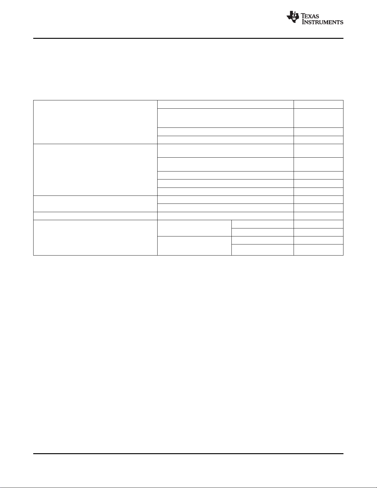
TMS320C5514
SPRS646B–AUGUST 2010–REVISED AUGUST 2010
www.ti.com
5 Device Operating Conditions
For the device maximum operating frequency, see Section 3.6.2, Device and Development-Support Tool
Nomenclature.
5.1 Absolute Maximum Ratings Over Operating Case Temperature Range (Unless Otherwise Noted)
Supply voltage ranges: Digital Core (CVDD, CV
Input and Output voltage ranges: VII/O, All pins with DV
Operating case temperature ranges, Tc: Commercial Temperature (default) -10°C to 70°C
Storage temperature range, T
Device Operating Life DSP Operating Frequency <70 °C 100,000 POH
Power-On Hours (POH)
(1) Stresses beyond those listed under "absolute maximum ratings" may cause permanent damage to the device. These are stress ratings
only, and functional operation of the device at these or any other conditions beyond those indicated under "recommended operating
conditions" is not implied. Exposure to absolute-maximum-rated conditions for extended periods may affect device reliability.
(2) All voltage values are with respect to V
(3) This information is provided solely for your convenience and does not extend or modify the warranty provided under TI’s standard terms
and conditions for TI semiconductor products.
(4) POH (Industrial Temperature) = 100,000 when the Maximum Core Supply Voltages are limited to 105% of the Nominal Core Supply
Voltages (For details on the Core Supplies, see Section 5.2, Recommended Operating Conditions).
(3)
stg
(1)
SS.
, USB_V
DDRTC
I/O, 1.8 V, 2.5 V, 2.75 V, 3.3 V (DV
DV
USB_V
) 3.3V USB supplies USB PHY (USB_V
DDRTC
DDPLL
, USB_V
DDA3P3
(2)
)
DDIO
DD1P3
, DV
(2)
)
, –0.5 V to 4.2 V
DDEMIF
DDOSC
,
–0.5 V to 1.7 V
LDOI –0.5 V to 4.2 V
Analog, 1.3 V (V
USB_V
DDPLL
DDA_PLL
or USB_V
VOI/O, All pins with DV
USB_V
DDPLL
or USB_V
, USB_V
DDIO
DDA3P3
DDIO
DDA3P3
or DV
or DV
, V
DDA1P3
DDEMIF
as supply source
as supply source
DDEMIF
DDA_ANA
or USB_V
or USB_V
(2)
)
or –0.5 V to 4.2 V
DDOSC
or –0.5 V to 4.2 V
DDOSC
–0.5 V to 1.7 V
RTC_XI and RTC_XO –0.5 V to 1.7 V
VO, BG_CAP –0.5 V to 1.7 V
ANA_LDOO, DSP_LDOO, and USB_LDOO –0.5 V to 1.7 V
Industrial Temperature -40°C to 85°C
(default) –65°C to 150°C
(SYSCLK ) ≤100 MHz
≥70 °C - ≤85 °C 100,000 POH
DSP Operating Frequency <70 °C 100,000 POH
(SYSCLK):
>100 MHz - ≤120 MHz
≥70 °C - ≤85 °C 85,000 POH
(4)
60 Device Operating Conditions Copyright © 2010, Texas Instruments Incorporated
Submit Documentation Feedback
Product Folder Link(s): TMS320C5514
Page 61

TMS320C5514
www.ti.com
SPRS646B–AUGUST 2010–REVISED AUGUST 2010
5.2 Recommended Operating Conditions
MIN NOM MAX UNIT
60 or 75 MHz 0.998 1.15 V
100 or 120 MHz 1.24 1.3 1.43 V
(2)
(2)
Default
(Commercial)
0.7 * DV
DD
-0.3 0.3 * DV
-10 70 °C
(Industrial) -40 85 °C
1.05 V 0 60 or 75
1.3 V 0 100 or 120
DDIO
.
DDIO
DVDD+ 0.3 V
DD
(3)
(3)
is powered
Core Supplies
CV
DD
CV
DDRTC
USB_V
USB_V
V
DDA_ANA
V
DDA_PLL
USB_V
DD1P3
DDA1P3
DDPLL
Supply voltage, Digital Core
Supply voltage, RTC and RTC OSC 32.768 KHz 0.998 1.43 V
Supply voltage, Digital USB 1.24 1.3 1.43 V
Supply voltage, 1.3 V Analog USB 1.24 1.3 1.43 V
Supply voltage, 1.3 V Pwr Mgmt 1.24 1.3 1.43 V
Supply voltage, System PLL 1.24 1.3 1.43 V
Supply voltage, 3.3 V USB PLL 2.97 3.3 3.63 V
Supply voltage, I/O, 3.3 V 2.97 3.3 3.63 V
DV
DV
DV
DDIO
DDEMIF
DDRTC
Supply voltage, I/O, 2.75 V 2.48 2.75 3.02 V
Supply voltage, I/O, 2.5 V 2.25 2.5 2.75 V
I/O Supplies Supply voltage, I/O, 1.8 V 1.65 1.8 1.98 V
USB_V
USB_V
DDOSC
DDA3P3
Supply voltage, I/O, 3.3 V USB OSC 2.97 3.3 3.63 V
Supply voltage, I/O, 3.3 V Analog USB PHY 2.97 3.3 3.63 V
LDOI Supply voltage, Analog Pwr Mgmt and LDO Inputs 1.8 3.6 V
V
SS
V
SSRTC
USB_V
SSOSC
USB_V
SSPLL
USB_V
GND 0 0 0 V
(1)
V
IH
(1)
V
IL
T
c
F
SYSCLK
USB_V
USB_V
V
SSA_PLL
USB_V
V
SSA_ANA
SSA3P3
SSA1P3
SSREF
SS1P3
Supply ground, Digital I/O
Supply ground, RTC
Supply ground, USB OSC
Supply ground, USB PLL
Supply ground, 3.3 V Analog USB PHY
Supply ground, USB 1.3 V Analog USB PHY
Supply ground, USB Reference Current
Supply ground, System PLL
Supply ground, 1.3 V Digital USB PHY
Supply ground, Pwr Mgmt
High-level input voltage, 3.3, 2.75, 2.5, 1.8 V I/O
Low-level input voltage, 3.3, 2.75, 2.5, 1.8 V I/O
Operating case temperature
DSP Operating Frequency (SYSCLK)
(1) DVDDrefers to the pin I/O supply voltage. To determine the I/O supply voltage for each pin, see Section 3.5, Terminal Functions.
(2) The I2C pin SDA and SCL do not feature fail-safe I/O buffers. These pin could potentially draw current when the DV
down. Due to the fact that different voltage devices can be connected to I2C bus and the I2C inputs are LVCMOS, the level of logic 0
(low) and logic 1 (high) are not fixed and depend on DV
(3) For the device maximum operating frequency, see Section 3.6.2, Device and Development-Support Tool Nomenclature.
V
MHz
MHz
Copyright © 2010, Texas Instruments Incorporated Device Operating Conditions 61
Submit Documentation Feedback
Product Folder Link(s): TMS320C5514
Page 62

TMS320C5514
SPRS646B–AUGUST 2010–REVISED AUGUST 2010
5.3 Electrical Characteristics Over Recommended Ranges of Supply Voltage and Operating Temperature (Unless Otherwise Noted)
PARAMETER TEST CONDITIONS
Full speed: USB_DN and
(2)
USB_DP
V
OH
V
OL
High speed: USB_DN and
(2)
USB_DP
High-level output voltage, 3.3,
2.75, 2.5, 1.8 V I/O
Full speed: USB_DN and
(2)
USB_DP
High speed: USB_DN and
(2)
USB_DP
Low-level output voltage, 3.3,
2.75, 2.5, 1.8V I/O
Low-level output voltage, I2C
(3)
pins
IO = I
OH
IO = I
OL
VDD> 2 V, IOL= 3 mA 0 0.4 V
DVDD= 3.3 V 162 mV
V
HYS
Input hysteresis
(4)
DVDD= 2.5 V 141 mV
DVDD= 1.8 V 122 mV
USB_LDOO voltage 1.24 1.3 1.43 V
V
LDO
I
SD
ANA_LDOO voltage 1.24 1.3 1.43 V
DSP_LDOO voltage
DSP_LDO shutdown current
ANA_LDO shutdown current
USB_LDO shutdown current
DSP_LDO_V bit in the LDOCNTL register = 1 1.24 1.3 1.43 V
DSP_LDO_V bit in the LDOCNTL register = 0 0.998 1.05 1.15 V
(5)
LDOI = V
LDOI = V
LDOI = V
MIN
MIN
MIN
(5)
(5)
Input only pin, internal pulldown or pullup disabled -5 +5 mA
I
ILPU
Input current [DC] (except
(6)(7)
WAKEUP, and I2C pins)
DVDD= 3.3 V with internal pullup enabled
DVDD= 2.5 V with internal pullup enabled
DVDD= 1.8 V with internal pullup enabled
Input only pin, internal pulldown or pullup disabled -5 +5 mA
I
IHPD
Input current [DC] (except
(6)(7)
WAKEUP, and I2C pins)
DVDD= 3.3 V with internal pulldown enabled
DVDD= 2.5 V with internal pulldown enabled
DVDD= 1.8 V with internal pulldown enabled
IIH/ VI= VSSto DVDDwith internal pullups and
(7)
I
IL
Input current [DC], ALL pins -5 +5 mA
pulldowns disabled.
All Pins (except EMIF, and CLKOUT pins) -4 mA
(7)
I
OH
High-level output current [DC] DVDD= 1.8 V -5 mA
EMIF pins
CLKOUT pin
All Pins (except USB, EMIF, and CLKOUT pins) +4 mA
(7)
I
OL
Low-level output current [DC] DVDD= 1.8 V +5 mA
EMIF pins
CLKOUT pin
(1)
MIN TYP MAX UNIT
2.8 USB_V
360 440 mV
0.8 * DV
DD
0.0 0.3 V
–10 10 mV
250 mA
4 mA
25 mA
(8)
(8)
(8)
(8)
(8)
(8)
-59 to
-161
-31 to -93 mA
-14 to -44 mA
52 to 158 mA
27 to 83 mA
11 to 35 mA
DVDD= 3.3 V -6 mA
DVDD= 3.3 V -6 mA
DVDD= 1.8 V -4 mA
DVDD= 3.3 V +6 mA
DVDD= 3.3 V +6 mA
DVDD= 1.8 V +4 mA
DDA3P3
0.2 * DV
www.ti.com
DD
V
V
V
mA
(1) For test conditions shown as MIN, MAX, or TYP, use the appropriate value specified in the recommended operating conditions table.
(2) The USB I/Os adhere to the Universal Bus Specification Revision 2.0 (USB2.0 spec).
(3) VDDis the voltage to which the I2C bus pullup resistors are connected.
(4) Applies to all input pins except WAKEUP, I2C pins, and USB_MXI.
(5)
(6) IIapplies to input-only pins and bi-directional pins. For input-only pins, IIindicates the input leakage current. For bi-directional pins, I
indicates the input leakage current and off-state (Hi-Z) output leakage current.
I
(7) When CVDDpower is "ON", the pin bus-holders are disabled. For more detailed information, see Section 6.3.2, Digital I/O Behavior
When Core Power (CVDD) is Down.
(8) Applies only to pins with an internal pullup (IPU) or pulldown (IPD) resistor.
62 Device Operating Conditions Copyright © 2010, Texas Instruments Incorporated
Submit Documentation Feedback
Product Folder Link(s): TMS320C5514
Page 63

TMS320C5514
www.ti.com
SPRS646B–AUGUST 2010–REVISED AUGUST 2010
Electrical Characteristics Over Recommended Ranges of Supply Voltage and Operating Temperature
(Unless Otherwise Noted) (continued)
(9)
I
OZ
I/O Off-state output current All Pins (except USB) -10 +10 mA
Supply voltage, I/O, 3.3 V 2.2 mA
PARAMETER TEST CONDITIONS
I
OLBH
Bus Holder pull low current when
(10)
CVDDis powered "OFF"
Supply voltage, I/O, 2.75 V 1.6 mA
Supply voltage, I/O, 2.5 V 1.4 mA
Supply voltage, I/O, 1.8 V 0.72 mA
Supply voltage, I/O, 3.3 V -1.3 mA
I
OHBH
Bus Holder pull high current
(10)
when CVDDis powered "OFF"
Supply voltage, I/O, 2.75 V -0.97 mA
Supply voltage, I/O, 2.5 V -0.83 mA
Supply voltage, I/O, 1.8 V -0.46 mA
Active, CVDD= 1.3 V, DSP clock =100 or 120
MHz, Clock source = RTC on-chip Oscillator
Room Temp (25 °C), 75% DMAC + 25% ADD
(typical sine wave data switching)
Active, CVDD= 1.05 V, DSP clock =60 or 75 MHz,
Clock source = RTC on-chip Oscillator
Room Temp (25 °C) , 75% DMAC + 25% ADD
(typical data switching)
Active, CVDD= 1.3 V, DSP clock =100 of 120
MHz, Clock source = RTC on-chip Oscillator
Room Temp (25 °C), 75% DMAC + 25% NOP
(typical sine wave data switching)
Active, CVDD= 1.05 V, DSP clock =60 or 75 MHz,
Clock source = RTC on-chip Oscillator
Room Temp (25 °C) , 75% DMAC + 25% NOP
(typical data switching)
Standby, CVDD= 1.3 V, Master clock disabled,
Clock source = RTC on-chip Oscillator
Room Temp (25 °C), DARAM and SARAM in
active mode
Standby, CVDD= 1.05 V, Master clock disabled,
Clock source = RTC on-chip Oscillator
I
Core (CVDD) supply current
CDD
Room Temp (25 °C), DARAM and SARAM in
active mode
Standby, CVDD= 1.3 V, Master clock disabled,
Clock source = RTC on-chip Oscillator
Room Temp (25 °C), DARAM in retention and
SARAM in active mode
Standby, CVDD= 1.05 V, Master clock disabled,
Clock source = RTC on-chip Oscillator
Room Temp (25 °C), DARAM in retention and
SARAM in active mode
Standby, CVDD= 1.3 V, Master clock disabled,
Clock source = RTC on-chip Oscillator
Room Temp (25 °C), DARAM in active mode and
SARAM in retention
Standby, CVDD= 1.05 V, Master clock disabled,
Clock source = RTC on-chip Oscillator
Room Temp (25 °C), DARAM in active mode and
SARAM in retention
V
= 1.3 V
Analog PLL (V
current
C
I
C
o
Input capacitance 4 pF
Output capacitance 4 pF
DDA_PLL
) supply
DDA_PLL
Room Temp (25 °C), Phase detector = 170 kHz, 0.7 mA
VCO = 120 MHz
(9) IOZapplies to output-only pins, indicating off-state (Hi-Z) output leakage current.
(10) This parameter specifies the maximum strength of the Bus Holder and is needed to calculate the minimum strength of external pull-ups
and pull-downs.
(1)
MIN TYP MAX UNIT
0.22 mW/MHz
0.15 mW/MHz
0.22 mW/MHz
0.14 mW/MHz
0.44 mW
0.26 mW
0.40 mW
0.23 mW
0.28 mW
0.15 mW
Copyright © 2010, Texas Instruments Incorporated Device Operating Conditions 63
Submit Documentation Feedback
Product Folder Link(s): TMS320C5514
Page 64

TransmissionLine
4.0pF 1.85pF
Z0=50
(seeNote)
Ω
TesterPinElectronics
DataSheetTimingReferencePoint
Output
Under
Test
NOTE: The data sheet provides timing at the device pin. For output timing analysis, the tester pin electronics and its transmission line effects must be
taken into account.A transmissionline with a delay of2 ns can be usedto produce the desired transmissionline effect. Thetransmission line is
intended as a load only. It is not necessary to add or subtract the transmission line delay (2 ns) from the data sheet timings.
Input requirements in this data sheet are tested with an input slew rate of < 4 Volts per nanosecond (4 V/ns) at the device pin.
42 Ω 3.5nH
DevicePin
(seeNote)
V =V MAX(orV MAX)
ref IL OL
V =V MIN(orV MIN)
ref IH OH
TMS320C5514
SPRS646B–AUGUST 2010–REVISED AUGUST 2010
6 Peripheral Information and Electrical Specifications
6.1 Parameter Information
Figure 6-1. 3.3-V Test Load Circuit for AC Timing Measurements
The load capacitance value stated is only for characterization and measurement of AC timing signals. This
load capacitance value does not indicate the maximum load the device is capable of driving.
www.ti.com
6.1.1 1.8-V, 2.5-V, 2.75-V, and 3.3-V Signal Transition Levels
All rise and fall transition timing parameters are referenced to VILMAX and VIHMIN for input clocks, V
MAX and VOHMIN for output clocks.
Figure 6-2. Rise and Fall Transition Time Voltage Reference Levels
6.1.2 3.3-V Signal Transition Rates
All timings are tested with an input edge rate of 4 volts per nanosecond (4 V/ns).
6.1.3 Timing Parameters and Board Routing Analysis
The timing parameter values specified in this data manual do not include delays by board routing. As a
good board design practice, such delays must always be taken into account. Timing values may be
adjusted by increasing/decreasing such delays. TI recommends utilizing the available I/O buffer
information specification (IBIS) models to analyze the timing characteristics correctly. To properly use IBIS
models to attain accurate timing analysis for a given system, see the Using IBIS Models for Timing
Analysis application report (literature number SPRA839). If needed, external logic hardware such as
buffers may be used to compensate any timing differences.
6.2 Recommended Clock and Control Signal Transition Behavior
All clocks and control signals must transition between VIHand VIL(or between VILand VIH) in a monotonic
manner.
OL
64 Peripheral Information and Electrical Specifications Copyright © 2010, Texas Instruments Incorporated
Submit Documentation Feedback
Product Folder Link(s): TMS320C5514
Page 65

TMS320C5514
www.ti.com
6.3 Power Supplies
The device includes four core voltage-level supplies (CVDD, CV
several I/O supplies (DV
analog supplies (LDOI, V
, DV
DDIO
DDA_PLL
features that facilitate power sequencing—for example, Auto-Track and Slow-Start/Enable features. For
more information regarding TI's power management products and suggested devices to power TI DSPs,
visit www.ti.com/processorpower.
6.3.1 Power-Supply Sequencing
The device includes four core voltage-level supplies (CVDD, CV
several I/O supplies including—DV
The device does not require a specific power-up sequence. However, if the DSP_LDO is disabled
(DSP_LDO_EN = high) and an external regulator supplies power to the CPU Core (CVDD), the external
reset signal (RESET) must be held asserted until all of the supply voltages reach their valid operating
ranges.
Note: the external reset signal on the RESET pin must be held low until all of the power supplies reach
their operating voltage conditions.
The I/O design allows either the core supplies (CVDD, CV
supplies (DV
period of time while the other supply is not powered if the following constraints are met:
1. All maximum ratings and recommended operating conditions are satisfied.
2. All warnings about exposure to maximum rated and recommended conditions, particularly junction
temperature are satisfied. These apply to power transitions as well as normal operation.
3. Bus contention while core supplies are powered must be limited to 100 hours over the projected
lifetime of the device.
4. Bus contention while core supplies are powered down does not violate the absolute maximum ratings.
DDIO
, DV
DDEMIF
, DV
DDEMIF
, V
DDIO
DDRTC
, DV
DDA_ANA
, DV
DDEMIF
, USB_V
, USB_V
DDRTC
, and USB_V
, DV
DDRTC
, and USB_V
DDOSC
SPRS646B–AUGUST 2010–REVISED AUGUST 2010
, USB_V
DDRTC
, and USB_V
DDOSC
). Some TI power-supply devices include
DDPLL
, USB_V
DDRTC
, USB_V
, USB_V
DDRTC
DDA3P3
, and USB_V
DDOSC
DD1P3
) to be powered up for an indefinite
, USB_V
DD1P3
), as well as several
DDA3P3
, USB_V
DD1P3
DDA3P3
, USB_V
DDA1P3
DDA1P3
DDA1P3
.
) or the I/O
), and
), and
If the USB subsystem is not used, the USB Core (USB_V
supplies (USB_V
DDOSC
, USB_V
DDA3P3
, and USB_V
) can be powered off.
DDPLL
DD1P3
, USB_V
) and USB PHY and I/O level
DDA1P3
Note: If the device is powered up with the USB cable connected to an active USB host and the USB PHY
(USB_V
) is powered up before the USB Core (USB_V
DDA3P3
DD1P3
, USB_V
), the USB Core must be
DDA1P3
powered within 100 ms after the USB host detects the device has been attached.
A supply bus is powered up when the voltage is within the recommended operating range. It is powered
down when the voltage is below that range, either stable or while in transition.
Copyright © 2010, Texas Instruments Incorporated Peripheral Information and Electrical Specifications 65
Submit Documentation Feedback
Product Folder Link(s): TMS320C5514
Page 66

hhvgz
OR
GZ
HHV
A
Y
OR
PI
HHV
DVDD
PAD
hhvpi
HHV
TMS320C5514
SPRS646B–AUGUST 2010–REVISED AUGUST 2010
6.3.2 Digital I/O Behavior When Core Power (CVDD) is Down
With some exceptions (listed below), all digital I/O pins on the device have special features to allow
powering down of the Digital Core Domain (CVDD) without causing I/O contentions or floating inputs at the
pins (see Figure 6-3). The device asserts the internal signal called HHV high when power has been
removed from the Digital Core Domain (CVDD). Asserting the internal HHV signal causes the following
conditions to occur in any order:
• All output pin strong drivers to go to the high-impedance (Hi-Z) state
• Weak bus holders to be enabled to hold the pin at a valid high or low
• The internal pullups or pulldowns (IPUs/IPDs) on the I/O pins will be disabled
The exception pins that do not have this special feature are:
• Pins driven by the CV
driven by CV
do not need these special features]:
DDRTC
– RTC_XI, RTC_XO, RTC_CLKOUT, and WAKEUP
• USB Pins:
– USB_DP, USB_DM, USB_R1, USB_VBUS, USB_MXI, and USB_MXO
• Pins for the Analog Block:
– DSP_LDO_EN and BG_CAP
Power Domain [This power domain is "Always On"; therefore, the pins
DDRTC
www.ti.com
Figure 6-3. Bus Holder I/O Circuit
66 Peripheral Information and Electrical Specifications Copyright © 2010, Texas Instruments Incorporated
Submit Documentation Feedback
Product Folder Link(s): TMS320C5514
Page 67

TMS320C5514
www.ti.com
6.3.3 Power-Supply Design Considerations
Core and I/O supply voltage regulators should be located close to the DSP (or DSP array) to minimize
inductance and resistance in the power delivery path. Additionally, when designing for high-performance
applications utilizing the device, the PC board should include separate power planes for core, I/O,
V
DDA_ANA
and V
DDA_PLL
(which can share the same PCB power plane), and ground; all bypassed with
high–quality low–ESL/ESR capacitors.
6.3.4 Power-Supply Decoupling
In order to properly decouple the supply planes from system noise, place capacitors (caps) as close as
possible to the device. These caps need to be no more than 1.25 cm maximum distance from the device
power pins to be effective. Physically smaller caps, such as 0402, are better but need to be evaluated
from a yield/manufacturing point-of-view. Parasitic inductance limits the effectiveness of the decoupling
capacitors, therefore physically smaller capacitors should be used while maintaining the largest available
capacitance value.
Larger caps for each supply can be placed further away for bulk decoupling. Large bulk caps (on the order
of 10 mF) should be furthest away, but still as close as possible. Large caps for each supply should be
placed outside of the BGA footprint.
As with the selection of any component, verification of capacitor availability over the product's production
lifetime should be considered.
The recommended decoupling capacitance for the DSP core supplies should be 1 mF in parallel with
0.01-mF capacitor per supply pin.
SPRS646B–AUGUST 2010–REVISED AUGUST 2010
6.3.5 LDO Input Decoupling
The LDO inputs should follow the same decoupling guidelines as other power-supply pins above.
6.3.6 LDO Output Decoupling
The LDO circuits implement a voltage feedback control system which has been designed to optimize gain
and stability tradeoffs. As such, there are design assumptions for the amount of capacitance on the LDO
outputs. For proper device operation, the following external decoupling capacitors should be used when
the on-chip LDOs are enabled:
• ANA_LDOO– 1mF
• DSP_LDOO – 5mF ~ 10mF
• USB_LDOO – 1mF ~ 2mF
Copyright © 2010, Texas Instruments Incorporated Peripheral Information and Electrical Specifications 67
Submit Documentation Feedback
Product Folder Link(s): TMS320C5514
Page 68

RTC_XI RTC_XO
C1 C2
Crystal
32.768 kHz
V
SSRTC
CV
DDRTC
0.998-1.43 V
1.05/1.3 V
CV
DD
V
SS
TMS320C5514
SPRS646B–AUGUST 2010–REVISED AUGUST 2010
6.4 External Clock Input From RTC_XI, CLKIN, and USB_MXI Pins
The device DSP includes two options to provide an external clock input to the system clock generator:
• Use the on-chip real-time clock (RTC) oscillator with an external 32.768-kHz crystal connected to the
RTC_XI and RTC_XO pins.
• Use an external 11.2896-, 12.0-, or 12.288-MHz LVCMOS clock input fed into the CLKIN pin that
operates at the same voltage as the DV
supply (1.8-, 2.5-, 2.75-, or 3.3-V).
DDIO
The CLK_SEL pin determines which input is used as the clock source for the system clock generator. For
more details, see Section 4.5.1, Device and Peripheral Configurations at Device Reset. The crystal for the
RTC oscillator is not required if CLKIN is used as the system reference clock; however, the RTC must still
be powered. The RTC registers starting at I/O address 1900h will not be accessible without an RTC clock.
This includes the RTC Power Management Register which provides control to the on-chip LDOs and
WAKEUP and RTC_CLKOUT pins. Section 6.4.1, Real-Time Clock (RTC) On-Chip Oscillator With
External Crystal provides more details on using the RTC on-chip oscillator with an external crystal.
Section 6.4.2, CLKIN Pin With LVCMOS-Compatible Clock Input provides details on using an external
LVCMOS-compatible clock input fed into the CLKIN pin.
Additionally, the USB requires a reference clock generated using a dedicated on-chip oscillator with a
12-MHz external crystal connected to the USB_MXI and USB_MXO pins. The USB reference clock is not
required if the USB peripheral is not being used. Section 6.4.3, USB On-Chip Oscillator With External
Crystal provides details on using the USB on-chip oscillator with an external crystal.
6.4.1 Real-Time Clock (RTC) On-Chip Oscillator With External Crystal
www.ti.com
The on-chip oscillator requires an external 32.768-kHz crystal connected across the RTC_XI and RTC_XO
pins, along with two load capacitors, as shown in Figure 6-4. The external crystal load capacitors must be
connected only to the RTC oscillator ground pin (V
the VSSlead on the board between RTC_XI and RTC_XO as a shield to reduce direct capacitance
between RTC_XI and RTC_XO leads on the board. The CV
power supply as CVDD, or may be connected to a different supply that meets the recommended operating
conditions (see Section 5.2, Recommended Operating Conditions), if desired.
The crystal should be in fundamental-mode function, and parallel resonant, with a maximum effective
series resistance (ESR) specified in Table 6-1. The load capacitors, C1 and C2, are the total capacitance
of the circuit board and components, excluding the IC and crystal. The load capacitors values are usually
approximately twice the value of the crystal's load capacitance, CL, which is specified in the crystal
manufacturer's datasheet and should be chosen such that the equation is satisfied. All discrete
components used to implement the oscillator circuit should be placed as close as possible to the
associated oscillator pins (RTC_XI and RTC_XO) and to the V
68 Peripheral Information and Electrical Specifications Copyright © 2010, Texas Instruments Incorporated
Figure 6-4. 32.768-kHz RTC Oscillator
). Do not connect to board ground (VSS). Position
SSRTC
Submit Documentation Feedback
Product Folder Link(s): TMS320C5514
DDRTC
SSRTC
pin can be connected to the same
pin.
Page 69

( )
C C
1 2
C
L
C C
1 2
=
+
RTC_XI RTC_XO
C1 C2
Crystal
32.768 kHz
V
SSRTC
CV
DDRTC
0.998-1.43 V
1.05/1.3 V
CV
DD
V
SS
CLKIN
TMS320C5514
www.ti.com
SPRS646B–AUGUST 2010–REVISED AUGUST 2010
Table 6-1. Input Requirements for Crystal on the 32.768-kHz RTC Oscillator
PARAMETER MIN NOM MAX UNIT
Start-up time (from power up until oscillating at stable frequency of 32.768-kHz)
Oscillation frequency 32.768 kHz
ESR 100 kΩ
Maximum shunt capacitance 1.6 pF
Maximum crystal drive 1.0 mW
(1) The startup time is highly dependent on the ESR and the capacitive load of the crystal.
(1)
0.2 2 sec
6.4.2 CLKIN Pin With LVCMOS-Compatible Clock Input (Optional)
Note: If CLKIN is not used, the pin must be tied low.
A LVCMOS-compatible clock input of a frequency less than 24 MHz can be fed into the CLKIN pin for use
by the DSP system clock generator. The external connections are shown in Figure 6-5 and Figure 6-6.
The bootloader assumes that the CLKIN pin is connected to the LVCMOS-compatible clock source with a
frequency of 11.2896-, 12.0-, or 12.288-MHz. These frequencies were selected to support boot mode
peripheral speeds of 500 KHz for SPI and 400 KHz for I2C. These clock frequencies are achieved by
dividing the CLKIN value by 25 for SPI and by 32 for I2C. If a faster external clock is input, then these
boot modes will run at faster clock speeds. If the system design utilizes faster peripherals or these boot
modes are not used, CLKIN values higher than 12.288 MHz can be used. Note: The CLKIN pin operates
at the same voltage as the DV
In this configuration the RTC oscillator can be optionally disabled by connecting RTC_XI to CV
RTC_XO to ground (VSS). However, when the RTC oscillator is disabled the RTC registers starting at I/O
address 1900h will not be accessible. This includes the RTC Power Management Register which provides
control to the on-chip LDOs and WAKEUP and RTC_CLKOUT pins. Note: the RTC must still be powered
even if the RTC oscillator is disabled.
supply (1.8-, 2.5-, 2.75-, or 3.3-V).
DDIO
DDRTC
and
For more details on the RTC on-chip oscillator, see Section 6.4.1, Real-Time Clock (RTC) On-Chip
Oscillator With External Crystal.
Figure 6-5. LVCMOS-Compatible Clock Input With RTC Oscillator Enabled
Copyright © 2010, Texas Instruments Incorporated Peripheral Information and Electrical Specifications 69
Submit Documentation Feedback
Product Folder Link(s): TMS320C5514
Page 70

RTC_XI RTC_XO
CV
DDRTC
0.998-1.43 V
1.05/1.3 V
CV
DD
V
SS
CLKIN
V
SSRTC
USB_MXI USB_MXO
C1 C2
Crystal
12MHz
USB_V
SSOSC
USB_V
DDOSC
3.3V
3.3V
USB_V
DDA3P3
V
SS
TMS320C5514
SPRS646B–AUGUST 2010–REVISED AUGUST 2010
Figure 6-6. LVCMOS-Compatible Clock Input With RTC Oscillator Disabled
6.4.3 USB On-Chip Oscillator With External Crystal (Optional)
When using the USB, the USB on-chip oscillator requires an external 12-MHz crystal connected across
the USB_MXI and USB_MXO pins, along with two load capacitors, as shown in Figure 6-7. The external
crystal load capacitors must be connected only to the USB oscillator ground pin (USB_V
connect to board ground (VSS). The USB_V
USB_V
DDA3P3
.
The USB on-chip oscillator can be permanently disabled, via tie-offs, if the USB peripheral is not being
used. To permanently disable the USB oscillator, connect the USB_MXI pin to ground (VSS) and leave the
USB_MXO pin unconnected. The USB oscillator power pins (USB_V
be connected to ground, as shown in Figure 6-8.
pin can be connected to the same power supply as
DDOSC
DDOSC
and USB_V
SSOSC
SSOSC
www.ti.com
). Do not
) should also
When using an external 12-MHz oscillator, the external oscillator clock signal should be connected to the
USB_MXI pin and the amplitude of the oscillator clock signal must meet the VIHrequirement (see
Section 5.2, Recommended Operating Conditions). The USB_MXO is left unconnected and the
USB_V
signal is connected to board ground (VSS).
SSOSC
Figure 6-7. 12-MHz USB Oscillator
70 Peripheral Information and Electrical Specifications Copyright © 2010, Texas Instruments Incorporated
Submit Documentation Feedback
Product Folder Link(s): TMS320C5514
Page 71

USB_MXI USB_MXO
USB_V
SSOSC
USB_V
DDOSC
USB_V
DDA3P3
V
SS
( )
C C
1 2
C
L
C C
1 2
=
+
TMS320C5514
www.ti.com
The crystal should be in fundamental-mode operation, and parallel resonant, with a maximum effective
series resistance (ESR) specified in Table 6-2. The load capacitors, C1 and C2 are the total capacitance
of the circuit board and components, excluding the IC and crystal. The load capacitor value is usually
approximately twice the value of the crystal's load capacitance, CL, which is specified in the crystal
manufacturer's datasheet and should be chosen such that the equation below is satisfied. All discrete
components used to implement the oscillator circuit should be placed as close as possible to the
associated oscillator pins (USB_MXI and USB_MXO) and to the USB_V
SPRS646B–AUGUST 2010–REVISED AUGUST 2010
Figure 6-8. Connections when USB Oscillator is Permanently Disabled
pin.
SSOSC
Table 6-2. Input Requirements for Crystal on the 12-MHz USB Oscillator
PARAMETER MIN NOM MAX UNIT
Start-up time (from power up until oscillating at stable frequency of 12 MHz)
Oscillation frequency 12 MHz
ESR 100 Ω
Frequency stability
Maximum shunt capacitance 5 pF
Maximum crystal drive 330 mW
(1) The startup time is highly dependent on the ESR and the capacitive load of the crystal.
(2) If the USB is used, a 12-MHz, ±100-ppm crystal is recommended.
(2)
(1)
0.100 10 ms
±100 ppm
Copyright © 2010, Texas Instruments Incorporated Peripheral Information and Electrical Specifications 71
Product Folder Link(s): TMS320C5514
Submit Documentation Feedback
Page 72

TMS320C5514
SPRS646B–AUGUST 2010–REVISED AUGUST 2010
6.5 Clock PLLs
The device DSP uses a software-programmable PLL to generate frequencies required by the CPU, DMA,
and peripherals. The reference clock for the PLL is taken from either the CLKIN pin or the RTC on-chip
oscillator (as specified through the CLK_SEL pin).
6.5.1 PLL Device-Specific Information
There is a minimum and maximum operating frequency for CLKIN, PLLOUT, and the system clock
(SYSCLK). The system clock generator must be configured not to exceed any of these constraints
documented in this section (certain combinations of external clock inputs, internal dividers, and PLL
multiply ratios are not supported).
Table 6-3. PLLC1 Clock Frequency Ranges
CLOCK SIGNAL NAME UNIT
(1)
CLKIN
RTC Clock 32.768 32.768 KHz
PLLIN 32.768 170 32.768 170 KHz
PLLOUT 60 120 60 120 MHz
SYSCLK 0.032768 60 or 75 0.032768 100 or 120 MHz
PLL_LOCKTIME 4 4 ms
(1) These CLKIN values are used when the CLK_SEL pin = 1.
CVDD= 1.05 V CVDD= 1.3 V
V
DDA_PLL
MIN MAX MIN MAX
= 1.3 V V
11.2896 11.2896
12 12 MHz
12.288 12.288
DDA_PLL
= 1.3 V
www.ti.com
The PLL has lock time requirements that must be followed. The PLL lock time is the amount of time
needed for the PLL to complete its phase-locking sequence.
6.5.2 Clock PLL Considerations With External Clock Sources
If the CLKIN pin is used to provide the reference clock to the PLL, to minimize the clock jitter a single
clean power supply should power both the device and the external clock oscillator circuit. The minimum
CLKIN rise and fall times should also be observed. For the input clock timing requirements, see
Section 6.5.3, Clock PLL Electrical Data/Timing (Input and Output Clocks).
Rise/fall times, duty cycles (high/low pulse durations), and the load capacitance of the external clock
source must meet the device requirements in this data manual (see Section 5.3, Electrical Characteristics
Over Recommended Ranges of Supply Voltage and Operating Temperature, and Section 6.5.3, Clock
PLL Electrical Data/Timing (Input and Output Clocks).
72 Peripheral Information and Electrical Specifications Copyright © 2010, Texas Instruments Incorporated
Submit Documentation Feedback
Product Folder Link(s): TMS320C5514
Page 73

CLKIN
2
3
4
4
1
1
CLKOUT
1
2
5
4
3
TMS320C5514
www.ti.com
SPRS646B–AUGUST 2010–REVISED AUGUST 2010
6.5.3 Clock PLL Electrical Data/Timing (Input and Output Clocks)
Table 6-4. Timing Requirements for CLKIN
NO. UNIT
1 t
2 t
3 t
4 t
c(CLKIN)
w(CLKINH)
w(CLKINL)
t(CLKIN)
Cycle time, external clock driven on 83.333, 83.333,
CLKIN or or
Pulse width, CLKIN high ns
Pulse width, CLKIN low ns
Transition time, CLKIN 4 4 ns
(1) The CLKIN frequency and PLL multiply factor should be chosen such that the resulting clock frequency is within the specific range for
CPU operating frequency.
(2) The reference points for the rise and fall transitions are measured at VILMAX and VIHMIN.
CVDD= 1.05 V CVDD= 1.3 V
MIN NOM MAX MIN NOM MAX
88.577, 88.577,
81.380 81.380
0.466 * 0.466 *
t
c(CLKIN)
0.466 * 0.466 *
t
c(CLKIN)
(1) (2)
(see Figure 6-9)
t
c(CLKIN)
t
c(CLKIN)
ns
Figure 6-9. CLKIN Timing
Table 6-5. Switching Characteristics Over Recommended Operating Conditions for CLKOUT
(1) (2)
(see Figure 6-10)
CVDD= 1.05 V CVDD= 1.3 V
NO. PARAMETER UNIT
1 t
2 t
3 t
4 t
5 t
c(CLKOUT)
w(CLKOUTH)
w(CLKOUTL)
t(CLKOUTR)
t(CLKOUTF)
Cycle time, CLKOUT P P 10 or 8.3 ns
Pulse duration, CLKOUT high ns
Pulse duration, CLKOUT low ns
Transition time (rise), CLKOUT 5 5 ns
Transition time (fall), CLKOUT 5 5 ns
V
t
c(CLKOUT)
t
c(CLKOUT)
(1) The reference points for the rise and fall transitions are measured at VOLMAX and VOHMIN.
(2) P = 1/SYSCLK clock frequency in nanoseconds (ns). For example, when SYSCLK frequency is 100 MHz, use P = 10 ns.
= 1.3 V V
DDA_PLL
DDA_PLL
= 1.3 V
MIN MAX MIN MAX
16.67 or
13.33
0.466 * 0.466 *
t
c(CLKOUT)
0.466 * 0.466 *
t
c(CLKOUT)
Figure 6-10. CLKOUT Timing
Copyright © 2010, Texas Instruments Incorporated Peripheral Information and Electrical Specifications 73
Submit Documentation Feedback
Product Folder Link(s): TMS320C5514
Page 74

TMS320C5514
SPRS646B–AUGUST 2010–REVISED AUGUST 2010
6.6 Direct Memory Access (DMA) Controller
The DMA controller is used to move data among internal memory, external memory, and peripherals
without intervention from the CPU and in the background of CPU operation.
The DSP includes a total of four DMA controllers. Aside from the DSP resources they can access, all four
DMA controllers are identical.
The DMA controller has the following features:
• Operation that is independent of the CPU.
• Four channels, which allow the DMA controller to keep track of the context of four independent block
transfers.
• Event synchronization. DMA transfers in each channel can be made dependent on the occurrence of
selected events.
• An interrupt for each channel. Each channel can send an interrupt to the CPU on completion of the
programmed transfer.
• Ping-Pong mode allows the DMA controller to keep track of double buffering context without CPU
intervention.
• A dedicated clock idle domain. The four device DMA controllers can be put into a low-power state by
independently turning off their input clocks.
6.6.1 DMA Channel Synchronization Events
The DMA controllers allow activity in their channels to be synchronized to selected events. The DSP
supports 20 separate synchronization events and each channel can be tied to separate sync events
independent of the other channels. Synchronization events are selected by programming the CHnEVT
field in the DMAn channel event source registers (DMAnCESR1 and DMAnCESR2).
www.ti.com
74 Peripheral Information and Electrical Specifications Copyright © 2010, Texas Instruments Incorporated
Submit Documentation Feedback
Product Folder Link(s): TMS320C5514
Page 75

TMS320C5514
www.ti.com
6.7 Reset
The device has two main types of reset: hardware reset and software reset.
Hardware reset is responsible for initializing all key states of the device. It occurs whenever the RESET
pin is asserted or when the internal power-on-reset (POR) circuit deasserts an internal signal called
POWERGOOD. The device's internal POR is a voltage comparator that monitors the DSP_LDOO pin
voltage and generates the internal POWERGOOD signal when the DSP_LDO is enabled externally by the
DSP_LDO_EN pin. POWERGOOD is asserted when the DSP_LDOO voltage is above a minimum
threshold voltage provided by the bandgap. When the DSP_LDO is disabled (DSP_LDO_EN is high), the
internal voltage comparator becomes inactive, and the POWERGOOD signal logic level is immediately set
high. The RESET pin and the POWERGOOD signal are internally combined with a logical AND gate to
produce an (active low) hardware reset (see Figure 6-11, Power-On Reset Timing Requirements and
Figure 6-12, Reset Timing Requirements).
There are two types of software reset: the CPU's software reset instruction and the software control of the
peripheral reset signals. For more information on the CPU's software reset instruction, see the
TMS320C55x CPU 3.0 CPU Reference Guide (literature number: SWPU073). In all the device
documentation, all references to "reset" refer to hardware reset. Any references to software reset will
explicitly state software reset.
The device RTC has one additional type of reset, a power-on-reset (POR) for the registers in the RTC
core. This POR monitors the voltage of CV
to the RTC core.
SPRS646B–AUGUST 2010–REVISED AUGUST 2010
and resets the RTC registers when power is first applied
DDRTC
6.7.1 Power-On Reset (POR) Circuits
The device includes two power-on reset (POR) circuits, one for the RTC (RTC POR) and another for the
rest of the chip (MAIN POR).
6.7.1.1 RTC Power-On Reset (POR)
The RTC POR ensures that the flip-flops in the CV
powerup. In particular, the RTCNOPWR register is reset by this POR and is used to indicate that the RTC
time registers need to be initialized with the current time and date when power is first applied.
6.7.1.2 Main Power-On Reset (POR)
The device includes an analog power-on reset (POR) circuit that keeps the DSP in reset until specific
voltages have reached predetermined levels. When the DSP_LDO is enabled externally by the
DSP_LDO_EN pin, the output of the POR circuit, POWERGOOD, is held low until the following conditions
are satisfied:
• LDOI is powered and the bandgap is active for at least approximately 8 ms
• VDD_ANA is powered for at least approximately 4 ms
• DSP_LDOO is above a threshold of approximately 950 mV (see Note:)
Once these conditions are met, the internal POWERGOOD signal is set high. The POWERGOOD signal
is internally combined with the RESET pin signal, via an AND-gate, to produce the DSP subsystem's
global reset. This global reset is the hardware reset for the whole chip, except the RTC. When the global
reset is deasserted (high), the boot sequence starts. For more detailed information on the boot sequence,
see Section 4.4, Boot Sequence.
DDRTC
power domain have an initial state upon
When the DSP_LDO is disabled (DSP_LDO_EN pin = 1), the voltage monitoring on the DSP_LDOO pin is
de-activated and the POWERGOOD signal is immediately set high. The RESET pin will be the sole
source of hardware reset.
Note: The POR comparator has hysteresis, so the threshold voltage becomes approximately 850 mV after
POWERGOOD signal is set high.
Copyright © 2010, Texas Instruments Incorporated Peripheral Information and Electrical Specifications 75
Submit Documentation Feedback
Product Folder Link(s): TMS320C5514
Page 76

TMS320C5514
SPRS646B–AUGUST 2010–REVISED AUGUST 2010
6.7.1.3 Reset Pin (RESET)
The device can receive an external reset signal on the RESET pin. As specified above in , Main Power-On
Reset, the RESET pin is combined with the internal POWERGOOD signal, that is generated by the MAIN
POR, via an AND-gate. The output of the AND gate provides the hardware reset to the chip. The RESET
pin may be tied high and the MAIN POR can provide the hardware reset in case DSP_LDO is enabled
(DSP_LDO_EN = 0), but an external hardware reset must be provided via the RESET pin when the
DSP_LDO is disabled (DSP_LDO_EN = 1).
Once the hardware reset is applied, the DSP clock generator is enabled and the DSP starts the boot
sequence. For more information on the boot sequence, see Section 4.4, Boot Sequence.
6.7.2 Pin Behavior at Reset
During normal operation, pins are controlled by the respective peripheral selected in the External Bus
Selection Register (EBSR) register. During power-on reset and reset, the behavior of the output pins
changes and is categorized as follows:
High Group: EM_CS4, EM_CS5, EM_CS2, EM_CS3, EM_DQM0, EM_DQM1, EM_OE, EM_WE,
•
SPI_CS3, RSV15, RSV14, XF
Low Group: SPI_CLK, EM_R/W, MMC0_CLK/I2S0_CLK/GP[0], MMC1_CLK/I2S1_CLK/GP[6],
•
RSV12
Z Group: EM_D[15:0], EMU[1:0], SCL, SDA, SPI_RX, SPI_TX, I2S2_RX/GP[20]/SPI_RX,
•
I2S2_DX/GP[27]/SPI_TX, I2S2_RTS/GP[28]/I2S3_CLK, I2S2_CTS/GP[29]/I2S3_RS,
I2S2_RXD/GP[30]/I2S3_RX, I2S2_TXD/GP[31]/I2S3_DX, GP[12], GP[13], GP[14], GP[15], GP[16],
GP[17], I2S2_CLK/GP[18]/SPI_CLK,/I2S2_FS/GP[19]/SPI_CS0, RTC_CLKOUT,
MMC0_CMD/I2S0_FS/GP[1], MMC0_D0/I2S0_DX/GP[2], MMC0_D1/I2S0_RX/GP[3],
MMC0_D2/GP[4], MMC0_D3/GP[5], MMC1_CMD/I2S1_FS/GP[7], MMC1_D0/2S1_DX/GP[8],
MMC1_D1/I2S1_RX/GP[9], MMC1_D2/GP[10], MMC1_D3/GP[11], TDO, WAKEUP
CLKOUT Group: CLKOUT, SPI_CS1
•
SYNCH 0→1 Group: SPI_CS0, SPI_CS2, RSV13
•
SYNCH 1→0 Group: RSV10, RSV11
•
SYNCH X→1 Group: EM_BA[1:0]
•
SYNCH X→0 Group: EM_A[20:0]
•
www.ti.com
76 Peripheral Information and Electrical Specifications Copyright © 2010, Texas Instruments Incorporated
Submit Documentation Feedback
Product Folder Link(s): TMS320C5514
Page 77

LOW Group
HIGHGroup
Z Group
RESET
SYNCH X 0→
Group
SYNCH X 1→
Group
SYNCH 0 1→
Group
SYNCH 1 0→
Group
64k + 8 clocks if CLK_SEL = 1,
32 + 8 clocks if CLK_SEL = 0
CLKOUT
POWERGOOD
(Internal)
POWERGOOD
(Internal)
and RESET
TMS320C5514
www.ti.com
SPRS646B–AUGUST 2010–REVISED AUGUST 2010
6.7.3 Reset Electrical Data/Timing
Table 6-6. Timing Requirements for Reset (see Figure 6-11 and Figure 6-12)
NO. UNIT
1 t
w(RSTL)
Pulse duration, RESET low 3P 3P ns
CVDD= 1.05 V CVDD= 1.3 V
MIN MAX MIN MAX
Figure 6-11. Power-On Reset Timing Requirements
Copyright © 2010, Texas Instruments Incorporated Peripheral Information and Electrical Specifications 77
Submit Documentation Feedback
Product Folder Link(s): TMS320C5514
Page 78

POWERGOOD
(Internal)
LOW Group
HIGHGroup
Z Group
RESET
POWERGOOD and RESET
(I )nternal
SYNCH X 0→
Group
SYNCH X 1→
Group
SYNCH 0 1→
Group
SYNCH 1 0→
Group
64k + 8 clocks if CLK_SEL = 1,
32 + 8 clocks if CLK_SEL = 0
CLKOUT
TMS320C5514
SPRS646B–AUGUST 2010–REVISED AUGUST 2010
www.ti.com
Figure 6-12. Reset Timing Requirements
78 Peripheral Information and Electrical Specifications Copyright © 2010, Texas Instruments Incorporated
Submit Documentation Feedback
Product Folder Link(s): TMS320C5514
Page 79

1
2
INTx
TMS320C5514
www.ti.com
SPRS646B–AUGUST 2010–REVISED AUGUST 2010
6.8 Wake-up Events, Interrupts, and XF
The device has a number of interrupts to service the needs of its peripherals. The interrupts can be
selectively enabled or disabled.
6.8.1 Interrupts Electrical Data/Timing
Table 6-7. Timing Requirements for Interrupts
NO. UNIT
1 t
w(INTH)
2 t
w(INTL)
(1) P = 1/SYSCLK clock frequency in ns. For example, when the CPU core is clocked at 100 MHz, use P = 10 ns. For example, when the
CPU core is clocked att 120 MHz, use P = 8.3 ns.
Pulse duration, interrupt high CPU active 2P ns
Pulse duration, interrupt low CPU active 2P ns
Figure 6-13. External Interrupt Timings
(1)
(see Figure 6-13)
CVDD= 1.05 V
CVDD= 1.3 V
MIN MAX
6.8.2 Wake-Up From IDLE Electrical Data/Timing
Table 6-8. Timing Requirements for Wake-Up From IDLE (see Figure 6-14)
CVDD= 1.05 V
NO. UNIT
1 t
w(WKPL)
Table 6-9. Switching Characteristics Over Recommended Operating Conditions For Wake-Up From
NO. PARAMETER UNIT
t
d(WKEVTH-C
2 IDLE3 Mode with SYSCLKDIS = 1,
KLGEN)
(1) D = 1/ External Clock Frequency (CLKIN).
(2) C = 1/RTCCLK= 30.5 ms. RTCCLK is the clock output of the 32.768-kHz RTC oscillator.
(3) P = 1/SYSCLK clock frequency in ns. For example, when the CPU core is clocked at 100 MHz, use P = 10 ns.
(4) Assumes the internal LDOs are used with a 0.1uF bandgap capacitor.
Pulse duration, WAKEUP or INTx low, SYSCLKDIS = 1 10 ns
(1)(2)(3)(4)
IDLE
Delay time, wake-up event high to CPU
active
(see Figure 6-14)
IDLE3 Mode with SYSCLKDIS = 1,
WAKEUP or INTx event, CLK_SEL = D ns
1
WAKEUP or INTx event, CLK_SEL = C ns
0
IDLE2 Mode; INTx event 3P ns
CVDD= 1.3 V
MIN MAX
CVDD= 1.05 V
CVDD= 1.3 V
MIN TYP MAX
Copyright © 2010, Texas Instruments Incorporated Peripheral Information and Electrical Specifications 79
Submit Documentation Feedback
Product Folder Link(s): TMS320C5514
Page 80
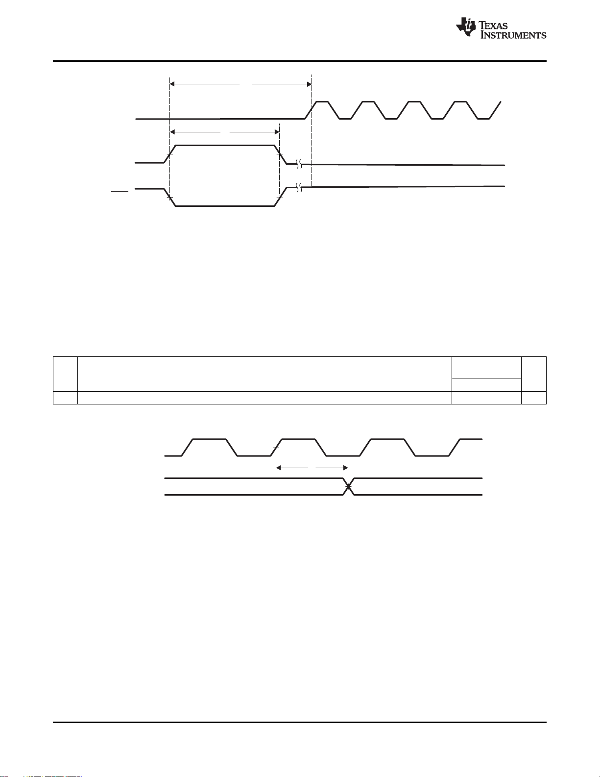
2
CLKOUT
INTx
WAKEUP
1
1
CLKOUT
(A)
XF
TMS320C5514
SPRS646B–AUGUST 2010–REVISED AUGUST 2010
A. INT[1:0] can only be used as a wake-up event for IDLE3 and IDLE2 modes.
B. RTC interrupt (internal signal) can be used as wake-up event for IDLE3 and IDLE2 modes.
C. Any unmasked interrupt can be used to exit the IDLE2 mode.
D. CLKOUT reflects either the CPU clock, USB PHY, or PLL clock dependent on the setting of the CLOCKOUT Clock
Source Register. For this diagram, CLKOUT refers to the CPU clock.
www.ti.com
Figure 6-14. Wake-Up From IDLE Timings
6.8.3 XF Electrical Data/Timing
Table 6-10. Switching Characteristics Over Recommended Operating Conditions For XF
(see Figure 6-15)
CVDD= 1.05 V
NO. PARAMETER UNIT
1 t
d(XF)
(1) P = 1/SYSCLK clock frequency in ns. For example, when the CPU core is clocked at 100 MHz, use P = 10 ns.
(2) C = 1/RTCCLK= 30.5 ms. RTCCLK is the clock output of the 32.768-kHz RTC oscillator.
Delay time, CLKOUT high to XF high 0 10.2 ns
CVDD= 1.3 V
(1) (2)
MIN MAX
A. CLKOUT reflects either the CPU clock, USB PHY, or PLL clock dependent on the setting of the CLOCKOUT Clock
Source Register. For this diagram, CLKOUT refers to the CPU clock.
Figure 6-15. XF Timings
80 Peripheral Information and Electrical Specifications Copyright © 2010, Texas Instruments Incorporated
Submit Documentation Feedback
Product Folder Link(s): TMS320C5514
Page 81

TMS320C5514
www.ti.com
6.9 External Memory Interface (EMIF)
The device supports several memories and external device interfaces, including: NOR Flash, NAND
Flash, SRAM, Non-Mobile SDRAM, and Mobile SDRAM (mSDRAM).
Note: The device can support non-mobile SDRAM under certain circumstances. The device also always
uses mobile SDRAM initialization, but it is able to support SDRAM memories that ignore the BA0 and BA1
pins for the 'load mode register' command. During the mobile SDRAM initialization, the device issues the
'load mode register' initialization command to two different addresses that differ in only the BA0 and BA1
address bits. These registers are the Extended Mode register and the Mode register. The Extended mode
register exists only in mSDRAM and not in non-mSDRAM. If a non-mobile SDRAM memory ignores bits
BA0 and BA1, the second loaded register value overwrites the first, leaving the desired value in the Mode
register and the non-mobile SDRAM will work with the device.
The EMIF provides an 8-bit or 16-bit data bus, an address bus width up to 21 bits, and 6 chip selects,
along with memory control signals.
The EM_A[20:15] address signals are multiplexed with the GPIO peripheral and controlled by the External
Bus Selection Register (EBSR). For more detail on the pin muxing, see the Section 4.6.1, External Bus
Selection Register (EBSR).
6.9.1 EMIF Asynchronous Memory Support
The EMIF supports asynchronous:
• SRAM memories
• NAND Flash memories
• NOR Flash memories
SPRS646B–AUGUST 2010–REVISED AUGUST 2010
The EMIF data bus can be configured for both 8- or 16-bit width. The device supports up to 21 address
lines and four external wait/interrupt inputs. Up to four asynchronous chip selects are supported by EMIF
(EM_CS[5:2]).
Each chip select has the following individually programmable attributes:
• Data bus width
• Read cycle timings: setup, hold, strobe
• Write cycle timings: setup, hold, strobe
• Bus turn around time
• Extended Wait Option With Programmable Timeout
• Select Strobe Option
• NAND flash controller supports 1-bit and 4-bit ECC calculation on blocks of 512 bytes
6.9.2 EMIF Non-Mobile and Mobile Synchronous DRAM Memory Supported
The EMIF supports 16-bit non-mobile and mobile single data rate (SDR) SDRAM in addition to the
asynchronous memories listed in Section 6.9.1, EMIF Asynchronous Memory Support. The supported
SDRAM and mobile SDRAM configurations are:
• One, two, and four bank SDRAM/mSDRAM devices
• Supports devices with eight, nine, ten, and eleven column addresses
• CAS latency of two or three clock cycles
• 16-bit data-bus width
• 3.3/2.75/2.5/1.8 -V LVCMOS interface that is separate from the rest of the chip I/Os.
• One (EM_CS0) or two (EM_CS[1:0]) chip selects
Additionally, the SDRAM/mSDRAM interface of EMIF supports placing the SDRAM/mSDRAM in
"Self-Refresh" and "Powerdown Modes". Self-Refresh mode allows the SDRAM/mSDRAM to be put into a
Copyright © 2010, Texas Instruments Incorporated Peripheral Information and Electrical Specifications 81
Submit Documentation Feedback
Product Folder Link(s): TMS320C5514
Page 82

TMS320C5514
SPRS646B–AUGUST 2010–REVISED AUGUST 2010
low-power state while still retaining memory contents; since the SDRAM/mSDRAM will continue to refresh
itself even without clocks from the DSP. Powerdown mode achieves even lower power, except the DSP
must periodically wake the SDRAM/mSDRAM up and issue refreshes if data retention is required. To
achieve the lowest power consumption, the SDRAM/mSDRAM interface has configurable slew rate on the
EMIF pins.
The device has limitations to the clock frequency on the EM_SDCLK pin based on the CVDDand
DV
DDEMIF
.
• The clock frequency on the EM_SDCLK pin can be configured either as SYSCLK (DSP Operating
Frequency) or SYSCLK/2 via bit 0 of the ECDR Register (0x1C26h)
• When CVDD= 1.3 V and DV
DDEMIF
= 3.3 V, 2.75 V, or 2.5 V, the max clock frequency on the
EM_SDCLK pin is limited to 100 MHz (EM_SDCLK ≤ 100 MHz). Therefore, if SYSCLK ≤ 100 MHz, the
EM_SDCLK can be configured either as SYSCLK or SYSCLK/2, but if SYSCLK > 100 MHz, the
EM_SDCLK must be configured as SYSCLK/2.
• When CVDD=1.05 V, and DV
DDEMIF
= 3.3 V, 2.75 V, or 2.5 V, the max clock frequency on the
EM_SDCLK pin is limited to 60 MHz (EM_SDCLK ≤ 60 MHz). Therefore, if SYSCLK ≤ 60 MHz, the
EM_SDCLK can be configured as either SYSCLK or SYSCLK/2, but if SYSCLK > 60 MHz, the
EM_SDCLK must be configured as SYSCLK/2.
• When DV
DDEMIF
= 1.8 V, regardless of the CVDDvoltage, the clock frequency on the EM_SDCLK pin
must be configured as SYSCLK/2.
6.9.3 EMIF Peripheral Register Description(s)
www.ti.com
Table 6-11 shows the EMIF registers.
Table 6-11. External Memory Interface (EMIF) Peripheral Registers
HEX ADDRESS ACRONYM
RANGE
1000h REV Revision Register
1001h STATUS Status Register
1004h AWCCR1 Asynchronous Wait Cycle Configuration Register 1
1005h AWCCR2 Asynchronous Wait Cycle Configuration Register 2
1008h SDCR1 SDRAM/mSDRAM Configuration Register 1
1009h SDCR2 SDRAM/mSDRAM Configuration Register 2
100Ch SDRCR SDRAM/mSDRAM Refresh Control Register
1010h ACS2CR1 Asynchronous CS2 Configuration Register 1
1011h ACS2CR2 Asynchronous CS2 Configuration Register 2
1014h ACS3CR1 Asynchronous CS3 Configuration Register 1
1015h ACS3CR2 Asynchronous CS3 Configuration Register 2
1018h ACS4CR1 Asynchronous CS4 Configuration Register 1
1019h ACS4CR2 Asynchronous CS4 Configuration Register 2
101Ch ACS5CR1 Asynchronous CS5 Configuration Register 1
101Dh ACS5CR2 Asynchronous CS5 Configuration Register 2
1020h SDTIMR1 SDRAM/mSDRAM Timing Register 1
1021h SDTIMR2 SDRAM/mSDRAM Timing Register 2
103Ch SDSRETR SDRAM/mSDRAM Self Refresh Exit Timing Register
1040h EIRR EMIF Interrupt Raw Register
1044h EIMR EMIF Interrupt Mask Register
1048h EIMSR EMIF Interrupt Mask Set Register
104Ch EIMCR EMIF Interrupt Mask Clear Register
REGISTER NAME
(1)
(1) Before reading or writing to the EMIF registers, be sure to set the BYTEMODE bits to 00b in the EMIF system control register to enable
word accesses to the EMIF registers.
82 Peripheral Information and Electrical Specifications Copyright © 2010, Texas Instruments Incorporated
Submit Documentation Feedback
Product Folder Link(s): TMS320C5514
Page 83

TMS320C5514
www.ti.com
Table 6-11. External Memory Interface (EMIF) Peripheral Registers (continued)
HEX ADDRESS ACRONYM
RANGE
1060h NANDFCR NAND Flash Control Register
1064h NANDFSR1 NAND Flash Status Register 1
1065h NANDFSR2 NAND Flash Status Register 2
1068h PGMODECTRL1 Page Mode Control Register 1
1069h PGMODECTRL2 Page Mode Control Register 2
1070h NCS2ECC1 NAND Flash CS2 1-Bit ECC Register 1
1071h NCS2ECC2 NAND Flash CS2 1-Bit ECC Register 2
1074h NCS3ECC1 NAND Flash CS3 1-Bit ECC Register 1
1075h NCS3ECC2 NAND Flash CS3 1-Bit ECC Register 2
1078h NCS4ECC1 NAND Flash CS4 1-Bit ECC Register 1
1079h NCS4ECC2 NAND Flash CS4 1-Bit ECC Register 2
107Ch NCS5ECC1 NAND Flash CS5 1-Bit ECC Register 1
107Dh NCS5ECC2 NAND Flash CS5 1-Bit ECC Register 2
10BCh NAND4BITECCLOAD NAND Flash 4-Bit ECC Load Register
10C0h NAND4BITECC1 NAND Flash 4-Bit ECC Register 1
10C1h NAND4BITECC2 NAND Flash 4-Bit ECC Register 2
10C4h NAND4BITECC3 NAND Flash 4-Bit ECC Register 3
10C5h NAND4BITECC4 NAND Flash 4-Bit ECC Register 4
10C8h NAND4BITECC5 NAND Flash 4-Bit ECC Register 5
10C9h NAND4BITECC6 NAND Flash 4-Bit ECC Register 6
10CCh NAND4BITECC7 NAND Flash 4-Bit ECC Register 7
10CDh NAND4BITECC8 NAND Flash 4-Bit ECC Register 8
10D0h NANDERRADD1 NAND Flash 4-Bit ECC Error Address Register 1
10D1h NANDERRADD2 NAND Flash 4-Bit ECC Error Address Register 2
10D4h NANDERRADD3 NAND Flash 4-Bit ECC Error Address Register 3
10D5h NANDERRADD4 NAND Flash 4-Bit ECC Error Address Register 4
10D8h NANDERRVAL1 NAND Flash 4-Bit ECC Error Value Register 1
10D9h NANDERRVAL2 NAND Flash 4-Bit ECC Error Value Register 2
10DCh NANDERRVAL3 NAND Flash 4-Bit ECC Error Value Register 3
10DDh NANDERRVAL4 NAND Flash 4-Bit ECC Error Value Register 4
SPRS646B–AUGUST 2010–REVISED AUGUST 2010
REGISTER NAME
Copyright © 2010, Texas Instruments Incorporated Peripheral Information and Electrical Specifications 83
Submit Documentation Feedback
Product Folder Link(s): TMS320C5514
Page 84

TMS320C5514
SPRS646B–AUGUST 2010–REVISED AUGUST 2010
6.9.4 EMIF Electrical Data/Timing CVDD= 1.05 V, DV
DDEMIF
= 3.3/2.75/2.5/1.8 V
www.ti.com
Table 6-12. Timing Requirements for EMIF SDRAM/mSDRAM Interface (see Figure 6-16 and Figure 6-17)
CVDD= 1.05 V
DV
NO. UNIT
DDEMIF
3.3/2.75/2.5 V
MIN MAX MIN MAX
19 t
su(DV-CLKH)
20 t
h(CLKH-DIV)
Table 6-13. Switching Characteristics Over Recommended Operating Conditions for EMIF
Input setup time, read data valid on EM_D[15:0] before
EM_SDCLK rising
Input hold time, read data valid on EM_D[15:0] after EM_SDCLK
rising
SDRAM/mSDRAM Interface
(1)
(see Figure 6-16 and Figure 6-17)
3.4 3.4 ns
1.2 1.2 ns
CVDD= 1.05 V CVDD= 1.05 V
NO. PARAMETER UNIT
DV
= 3.3/2.75/2.5 V DV
DDEMIF
MIN NOM MAX MIN NOM MAX
1 t
2 t
3 t
5 t
7 t
9 t
11 t
13 t
15 t
21 t
c(CLK)
w(CLK)
d(CLKH-CSV)
d(CLKH-DQMV)
d(CLKH-AV)
d(CLKH-DV)
d(CLKH-RASV)
d(CLKH-CASV)
d(CLKH-WEV)
d(CLKH-CKEV)
Cycle time, EMIF clock EM_SDCLK E 2E ns
Pulse width, EMIF clock EM_SDCLK high or
low
Delay time, EM_SDCLK rising to
EMA_CS[1:0] valid
Delay time, EM_SDCLK rising to
EM_DQM[1:0] valid
Delay time, EM_SDCLK rising to EM_A[20:0]
and EM_BA[1:0] valid
Delay time, EM_SDCLK rising to EM_D[15:0]
valid
Delay time, EM_SDCLK rising to EM_SDRAS
valid
Delay time, EM_SDCLK rising to EM_SDCAS
valid
Delay time, EM_SDCLK rising to EM_WE
valid
Delay time, EM_SDCLK rising to EM_SDCKE
valid
1.1 13.2 1.1 13.2 ns
1.1 13.2 1.1 13.2 ns
1.1 13.2 1.1 13.2 ns
1.1 13.2 1.1 13.2 ns
1.1 13.2 1.1 13.2 ns
1.1 13.2 1.1 13.2 ns
1.1 13.2 1.1 13.2 ns
1.1 13.2 1.1 13.2 ns
E/2 E ns
(1) E = SYSCLK period in ns. For more detail on the EM_SDCLK speed see Section 6.9.2, EMIF Non-Mobile and Mobile Synchronous
DRAM Memory Supported.
=
CVDD= 1.05 V
DV
DDEMIF
= 1.8 V
DDEMIF
= 1.8 V
84 Peripheral Information and Electrical Specifications Copyright © 2010, Texas Instruments Incorporated
Submit Documentation Feedback
Product Folder Link(s): TMS320C5514
Page 85

TMS320C5514
www.ti.com
Table 6-14. Timing Requirements for EMIF Asynchronous Memory
SPRS646B–AUGUST 2010–REVISED AUGUST 2010
(1)
(see Figure 6-18, Figure 6-20, and
Figure 6-21)
CVDD= 1.05 V
NO. UNIT
DV
MIN NOM MAX
READS and WRITES
2 t
w(EM_WAIT)
Pulse duration, EM_WAITx assertion and deassertion 2E ns
READS
12 t
su(EMDV-EMOEH)
13 t
h(EMOEH-EMDIV)
14 t
su (EMOEL-EMWAIT)
Setup time, EM_D[15:0] valid before EM_OE high 14.5 ns
Hold time, EM_D[15:0] valid after EM_OE high 0 ns
Setup time, EM_WAITx asserted before end of Strobe Phase
(2)
4E + 13 ns
WRITES
26 t
su (EMWEL-EMWAIT)
Setup time, EM_WAITx asserted before end of Strobe Phase
(2)
4E + 13 ns
(1) E = SYSCLK period in ns. For example, when SYSCLK is set to 100/120 MHz, E = 10/8.33 ns, respectively.
(2) Setup before end of STROBE phase (if no extended wait states are inserted) by which EM_WAITx must be asserted to add extended
wait states. Figure 6-20 and Figure 6-21 describe EMIF transactions that include extended wait states inserted during the STROBE
phase. However, cycles inserted as part of this extended wait period should not be counted; the 4E requirement is to the start of where
the HOLD phase would begin if there were no extended wait cycles.
= 3.3/2.75/2.5/1.8 V
DDEMIF
Copyright © 2010, Texas Instruments Incorporated Peripheral Information and Electrical Specifications 85
Submit Documentation Feedback
Product Folder Link(s): TMS320C5514
Page 86

TMS320C5514
SPRS646B–AUGUST 2010–REVISED AUGUST 2010
Table 6-15. Switching Characteristics Over Recommended Operating Conditions for EMIF Asynchronous Memory
Figure 6-21)
(3)
(1) (2)
(see Figure 6-19 and
www.ti.com
CVDD= 1.05 V
DV
= 3.3/2.75/2.5/1.8 V
NO. PARAMETER UNIT
DDEMIF
MIN NOM MAX
READS and WRITES
1 t
d(TURNAROUND)
Turn around time (TA)*E - 13 (TA)*E (TA)*E + 13 ns
READS
3 t
4 t
5 t
6 t
7 t
8 t
9 t
10 t
11 t
c(EMRCYCLE)
su(EMCEL-EMOEL)
h(EMOEH-EMCEH)
su(EMBAV-EMOEL)
h(EMOEH-EMBAIV)
su(EMBAV-EMOEL)
h(EMOEH-EMAIV)
w(EMOEL)
d(EMWAITH-EMOEH)
EMIF read cycle time (EW = 0) (RS+RST+RH)*E - 13 (RS+RST+RH)*E (RS+RST+RH)*E + 13 ns
EMIF read cycle time (EW = 1) (RS+RST+RH+(EWC*16))*E - 13 (RS+RST+RH+(EWC*16))*E (RS+RST+RH+(EWC*16))*E +139 ns
Output setup time, EM_CS[5:2] low to EM_OE low (SS = 0) (RS)*E-13 (RS)*E (RS)*E+13 ns
Output setup time, EM_CS[5:2] low to EM_OE low (SS = 1) -13 0 +13 ns
Output hold time, EM_OE high to EM_CS[5:2] high (SS = 0) (RH)*E - 13 (RH)*E (RH)*E + 13 ns
Output hold time, EM_OE high to EM_CS[5:2] high (SS = 1) -13 0 +13 ns
Output setup time, EM_BA[1:0] valid to EM_OE low (RS)*E-13 (RS)*E (RS)*E+13 ns
Output hold time, EM_OE high to EM_BA[1:0] invalid (RH)*E-13 (RH)*E (RH)*E+13 ns
Output setup time, EM_A[20:0] valid to EM_OE low (RS)*E-13 (RS)*E (RS)*E+13 ns
Output hold time, EM_OE high to EM_A[20:0] invalid (RH)*E-13 (RH)*E (RH)*E+13 ns
EM_OE active low width (EW = 0) (RST)*E-13 (RST)*E (RST)*E+13 ns
EM_OE active low width (EW = 1) (RST+(EWC*16))*E-13 (RST+(EWC*16))*E (RST+(EWC*16))*E+13 ns
Delay time from EM_WAITx deasserted to EM_OE high 4E-13 4E 4E+13 ns
WRITES
EMIF write cycle time (EW = 0) (WS+WST+WH)*E-13 (WS+WST+WH)*E (WS+WST+WH)*E+13 ns
15 t
16 t
17 t
18 t
19 t
20 t
21 t
22 t
c(EMWCYCLE)
su(EMCSL-EMWEL)
h(EMWEH-EMCSH)
su(EMBAV-EMWEL)
h(EMWEH-EMBAIV)
su(EMAV-EMWEL)
h(EMWEH-EMAIV)
w(EMWEL)
EMIF write cycle time (EW = 1) (WS+WST+WH+(EWC*16))*E - 13 (WS+WST+WH+(EWC*16))*E ns
Output setup time, EM_CS[5:2] low to EM_WE low (SS = 0) (WS)*E - 13 (WS)*E (WS)*E + 13 ns
Output setup time, EM_CS[5:2] low to EM_WE low (SS = 1) -13 0 +13 ns
Output hold time, EM_WE high to EM_CS[5:2] high (SS = 0) (WH)*E-13 (WH)*E (WH)*E+13 ns
Output hold time, EM_WE high to EM_CS[5:2] high (SS = 1) -13 0 +13 ns
Output setup time, EM_BA[1:0] valid to EM_WE low (WS)*E-13 (WS)*E (WS)*E+13 ns
Output hold time, EM_WE high to EM_BA[1:0] invalid (WH)*E-13 (WH)*E (WH)*E+13 ns
Output setup time, EM_A[20:0] valid to EM_WE low (WS)*E-13 (WS)*E (WS)*E+13 ns
Output hold time, EM_WE high to EM_A[20:0] invalid (WH)*E-13 (WH)*E (WH)*E+13 ns
EM_WE active low width (EW = 0) (WST)*E-13 (WST)*E (WST)*E+13 ns
EM_WE active low width (EW = 1) (WST+(EWC*16))*E-13 (WST+(EWC*16))*E (WST+(EWC*16))*E+13 ns
(WS+WST+WH+(EWC*16))*E +
13
(1) TA = Turn around, RS = Read setup, RST = Read strobe, RH = Read hold, WS = Write setup, WST = Write strobe, WH = Write hold, MEWC = Maximum external wait cycles. These
parameters are programmed via the Asynchronous Configuration and Asynchronous Wait Cycle Configuration Registers.
(2) E = SYSCLK period in ns. For example, when SYSCLK is set to 100/120 MHz, E = 10/8.33 ns, respectively.
(3) EWC = external wait cycles determined by EM_WAITx input signal. EWC supports the following range of values EWC[256-1]. Note that the maximum wait time before timeout is specified
by bit field MEWC in the Asynchronous Wait Cycle Configuration Register.
86 Peripheral Information and Electrical Specifications Copyright © 2010, Texas Instruments Incorporated
Submit Documentation Feedback
Product Folder Link(s): TMS320C5514
Page 87

TMS320C5514
www.ti.com
SPRS646B–AUGUST 2010–REVISED AUGUST 2010
Table 6-15. Switching Characteristics Over Recommended Operating Conditions for EMIF Asynchronous Memory (see Figure 6-19 and
Figure 6-21) (continued)
CVDD= 1.05 V
DV
= 3.3/2.75/2.5/1.8 V
NO. PARAMETER UNIT
MIN NOM MAX
23 t
24 t
25 t
d(EMWAITH-EMWEH)
su(EMDV-EMWEL)
h(EMWEH-EMDIV)
Delay time from EM_WAITx deasserted to EM_WE high 3E-13 4E 4E+13 ns
Output setup time, EM_D[15:0] valid to EM_WE low (WS)*E-13 (WS)*E (WS)*E+13 ns
Output hold time, EM_WE high to EM_D[15:0] invalid (WH)*E-13 (WH)*E (WH)*E+13 ns
DDEMIF
Copyright © 2010, Texas Instruments Incorporated Peripheral Information and Electrical Specifications 87
Submit Documentation Feedback
Product Folder Link(s): TMS320C5514
Page 88

TMS320C5514
SPRS646B–AUGUST 2010–REVISED AUGUST 2010
6.9.5 EMIF Electrical Data/Timing CVDD= 1.3 V, DV
DDEMIF
= 3.3/2.75/2.5/1.8 V
www.ti.com
Table 6-16. Timing Requirements for EMIF SDRAM/mSDRAM Interface (see Figure 6-16 and Figure 6-17)
CVDD= 1.3 V
NO. UNIT
DV
3.3/2.75/2.5 V
DDEMIF
=
MIN MAX MIN MAX
19 t
su(DV-CLKH)
20 t
h(CLKH-DIV)
Table 6-17. Switching Characteristics Over Recommended Operating Conditions for EMIF
Input setup time, read data valid on EM_D[15:0] before
EM_SDCLK rising
Input hold time, read data valid on EM_D[15:0] after EM_SDCLK
rising
SDRAM/mSDRAM Interface
(1)
(see Figure 6-16 and Figure 6-17)
3.4 3.4 ns
1.2 1.2 ns
CVDD= 1.3 V CVDD= 1.3 V
NO. PARAMETER UNIT
DV
= 3.3/2.75/2.5 V DV
DDEMIF
MIN NOM MAX MIN NOM MAX
1 t
2 t
3 t
5 t
7 t
9 t
11 t
13 t
15 t
21 t
c(CLK)
w(CLK)
d(CLKH-CSV)
d(CLKH-DQMV)
d(CLKH-AV)
d(CLKH-DV)
d(CLKH-RASV)
d(CLKH-CASV)
d(CLKH-WEV)
d(CLKH-CKEV)
Cycle time, EMIF clock EM_SDCLK E 2E ns
Pulse width, EMIF clock EM_SDCLK high or
low
Delay time, EM_SDCLK rising to
EMA_CS[1:0] valid
Delay time, EM_SDCLK rising to
EM_DQM[1:0] valid
Delay time, EM_SDCLK rising to EM_A[20:0]
and EM_BA[1:0] valid
Delay time, EM_SDCLK rising to EM_D[15:0]
valid
Delay time, EM_SDCLK rising to EM_SDRAS
valid
Delay time, EM_SDCLK rising to EM_SDCAS
valid
Delay time, EM_SDCLK rising to EM_WE
valid
Delay time, EM_SDCLK rising to EM_SDCKE
valid
1.1 7.77 1.1 7.77 ns
1.1 7.77 1.1 7.77 ns
1.1 7.77 1.1 7.77 ns
1.1 7.77 1.1 7.77 ns
1.1 7.77 1.1 7.77 ns
1.1 7.77 1.1 7.77 ns
1.1 7.77 1.1 7.77 ns
1.1 7.77 1.1 7.77 ns
E/2 E ns
(1) E = SYSCLK period in ns. For more detail on the EM_SDCLK speed see Section 6.9.2, EMIF Non-Mobile and Mobile Synchronous
DRAM Memory Supported.
CVDD= 1.3 V
DV
DDEMIF
= 1.8 V
DDEMIF
= 1.8 V
88 Peripheral Information and Electrical Specifications Copyright © 2010, Texas Instruments Incorporated
Submit Documentation Feedback
Product Folder Link(s): TMS320C5514
Page 89

TMS320C5514
www.ti.com
Table 6-18. Timing Requirements for EMIF Asynchronous Memory
SPRS646B–AUGUST 2010–REVISED AUGUST 2010
(1)
(see Figure 6-18, Figure 6-20, and
Figure 6-21)
CVDD= 1.3 V
NO. UNIT
DV
MIN NOM MAX
READS and WRITES
2 t
w(EM_WAIT)
Pulse duration, EM_WAITx assertion and deassertion 2E ns
READS
12 t
su(EMDV-EMOEH)
13 t
h(EMOEH-EMDIV)
14 t
su (EMOEL-EMWAIT)
Setup time, EM_D[15:0] valid before EM_OE high 11 ns
Hold time, EM_D[15:0] valid after EM_OE high 0 ns
Setup Time, EM_WAITx asserted before end of Strobe Phase
(2)
4E + 7.5 ns
WRITES
26 t
su (EMWEL-EMWAIT)
Setup Time, EM_WAITx asserted before end of Strobe Phase
(2)
4E + 7.5 ns
(1) E = SYSCLK period in ns. For example, when SYSCLK is set to 100/120 MHz, E = 10/8.33 ns, respectively.
(2) Setup before end of STROBE phase (if no extended wait states are inserted) by which EM_WAITx must be asserted to add extended
wait states. Figure 6-20 and Figure 6-21 describe EMIF transactions that include extended wait states inserted during the STROBE
phase. However, cycles inserted as part of this extended wait period should not be counted; the 4E requirement is to the start of where
the HOLD phase would begin if there were no extended wait cycles.
= 3.3/2.75/2.5/1.8 V
DDEMIF
Copyright © 2010, Texas Instruments Incorporated Peripheral Information and Electrical Specifications 89
Submit Documentation Feedback
Product Folder Link(s): TMS320C5514
Page 90

TMS320C5514
SPRS646B–AUGUST 2010–REVISED AUGUST 2010
Table 6-19. Switching Characteristics Over Recommended Operating Conditions for EMIF Asynchronous Memory
(1) (2) (3)
(see Figure 6-18,
www.ti.com
Figure 6-20, and Figure 6-21)
CVDD= 1.3 V
DV
= 3.3/2.75/2.5/1.8 V
NO. PARAMETER UNIT
MIN NOM MAX
READS and WRITES
1 t
d(TURNAROUND)
Turn around time (TA)*E - 7.5 (TA)*E (TA)*E + 7.5 ns
READS
3 t
4 t
5 t
6 t
7 t
8 t
9 t
10 t
11 t
c(EMRCYCLE)
su(EMCSL-EMOEL)
h(EMOEH-EMCSH)
su(EMBAV-EMOEL)
h(EMOEH-EMBAIV)
su(EMAV-EMOEL)
h(EMOEH-EMAIV)
w(EMOEL)
d(EMWAITH-EMOEH)
EMIF read cycle time (EW = 0) (RS+RST+RH)*E - 7.5 (RS+RST+RH)*E (RS+RST+RH)*E + 7.5 ns
EMIF read cycle time (EW = 1) (RS+RST+RH+(EWC*16))*E - 7.5 (RS+RST+RH+(EWC*16))*E (RS+RST+RH+(EWC*16))*E + 7.5 ns
Output setup time, EM_CS[5:2] low to EM_OE low (SS = 0) (RS)*E - 7.5 (RS)*E (RS)*E + 7.5 ns
Output setup time, EM_CS[5:2] low to EM_OE low (SS = 1) -7.5 0 +7.5 ns
Output hold time, EM_OE high to EM_CS[5:2] high (SS = 0) (RH)*E - 7.5 (RH)*E (RH)*E + 7.5 ns
Output hold time, EM_OE high to EM_CE[5:2] high (SS = 1) -7.5 0 +7.5 ns
Output setup time, EM_BA[1:0] valid to EM_OE low (RS)*E - 7.5 (RS)*E (RS)*E + 7.5 ns
Output hold time, EM_OE high to EM_BA[1:0] invalid (RH)*E - 7.5 (RH)*E (RH)*E + 7.5 ns
Output setup time, EM_A[20:0] valid to EM_OE low (RS)*E - 7.5 (RS)*E (RS)*E + 7.5 ns
Output hold time, EM_OE high to EM_A[20:0] invalid (RH)*E - 7.5 (RH)*E (RH)*E + 7.5 ns
EM_OE active low width (EW = 0) (RST)*E - 7.5 (RST)*E (RST)*E + 7.5 ns
EM_OE active low width (EW = 1) (RST+(EWC*16))*E - 7.5 (RST+(EWC*16))*E (RST+(EWC*16))*E + 7.5 ns
Delay time from EM_WAITx deasserted to EM_OE high 4E - 7.5 4E 4E + 7.5 ns
WRITES
EMIF write cycle time (EW = 0) (WS+WST+WH)*E - 7.5 (WS+WST+WH)*E (WS+WST+WH)*E + 7.5 ns
15 t
16 t
17 t
18 t
19 t
20 t
21 t
22 t
c(EMWCYCLE)
su(EMCSL-EMWEL)
h(EMWEH-EMCSH)
su(EMBAV-EMWEL)
h(EMWEH-EMBAIV)
su(EMAV-EMWEL)
h(EMWEH-EMAIV)
w(EMWEL)
EMIF write cycle time (EW = 1) (WS+WST+WH+(EWC*16))*E ns
Output setup time, EM_CS[5:2] low to EM_WE low (SS = 0) (WS)*E - 7.5 (WS)*E (WS)*E +7. 5 ns
Output setup time, EM_CS[5:2] low to EM_WE low (SS = 1) -7.5 0 +7.5 ns
Output hold time, EM_WE high to EM_CS[5:2] high (SS = 0) (WH)*E - 7.5 (WH)*E (WH)*E + 7.5 ns
Output hold time, EM_WE high to EM_CS[5:2] high (SS = 1) -7.5 0 +7.5 ns
Output setup time, EM_BA[1:0] valid to EM_WE low (WS)*E - 7.5 (WS)*E (WS)*E + 7.5 ns
Output hold time, EM_WE high to EM_BA[1:0] invalid (WH)*E - 7.5 (WH)*E (WH)*E + 7.5 ns
Output setup time, EM_A[20:0] valid to EM_WE low (WS)*E - 7.5 (WS)*E (WS)*E + 7.5 ns
Output hold time, EM_WE high to EM_A[20:0] invalid (WH)*E - 7.5 (WH)*E (WH)*E + 7.5 ns
EM_WE active low width (EW = 0) (WST)*E - 7.5 (WST)*E (WST)*E + 7.5 ns
EM_WE active low width (EW = 1) (WST+(EWC*16))*E - 7.5 (WST+(EWC*16))*E (WST+(EWC*16))*E + 7.5 ns
(WS+WST+WH+(EWC*16))*E - (WS+WST+WH+(EWC*16))*E +
7.5 7.5
DDEMIF
(1) TA = Turn around, RS = Read setup, RST = Read strobe, RH = Read hold, WS = Write setup, WST = Write strobe, WH = Write hold, MEWC = Maximum external wait cycles. These
parameters are programmed via the Asynchronous Configuration and Asynchronous Wait Cycle Configuration Registers.
(2) E = SYSCLK period in ns. For example, when SYSCLK is set to 100/120 MHz, E = 10/8.33 ns, respectively.
(3) EWC = external wait cycles determined by EM_WAITx input signal. EWC supports the following range of values EWC[256-1]. Note that the maximum wait time before timeout is specified
by bit field MEWC in the Asynchronous Wait Cycle Configuration Register.
90 Peripheral Information and Electrical Specifications Copyright © 2010, Texas Instruments Incorporated
Submit Documentation Feedback
Product Folder Link(s): TMS320C5514
Page 91

EM_SDCLK
EM_BA[1:0]
EM_A[20:0]
EM_D[15:0]
1
2 2
3
5
7
7
11
9
15
3
5
7
7
11
13
15
9
BASIC mSDRAM
WRITE OPERATION
EM_CS[1:0]
EM_DQM[1:0]
EM_SDRAS
EM_SDCAS
EM_WE
TMS320C5514
www.ti.com
SPRS646B–AUGUST 2010–REVISED AUGUST 2010
Table 6-19. Switching Characteristics Over Recommended Operating Conditions for EMIF Asynchronous Memory (see Figure 6-18, Figure 6-20,
and Figure 6-21) (continued)
CVDD= 1.3 V
DV
= 3.3/2.75/2.5/1.8 V
NO. PARAMETER UNIT
MIN NOM MAX
23 t
d(EMWAITH-EMWEH)
24 t
su(EMDV-EMWEL)
25 t
h(EMWEH-EMDIV)
Copyright © 2010, Texas Instruments Incorporated Peripheral Information and Electrical Specifications 91
Delay time from EM_WAITx deasserted to EM_WE high 3E - 7.5 4E 4E + 7.5 ns
Output setup time, EM_D[15:0] valid to EM_WE low (WS)*E - 7.5 (WS)*E (WS)*E + 7.5 ns
Output hold time, EM_WE high to EM_D[15:0] invalid (WH)*E - 7.5 (WH)*E (WH)*E + 7.5 ns
Figure 6-16. EMIF Basic SDRAM/mSDRAM Write Operation
Submit Documentation Feedback
Product Folder Link(s): TMS320C5514
DDEMIF
Page 92

EM_SDCLK
EM_BA[1:0]
EM_A[20:0]
EM_D[15:0]
1
2 2
3
5
7
7
11
13
19
20
3
5
7
7
11
13
17 17
2 EM_CLK Delay
BASIC mSDRAM
READ OPERATION
EM_CS[1:0]
EM_DQM[1:0]
EM_SDRAS
EM_SDCAS
EM_WE
EM_CS[5:2]
EM_BA[1:0]
13
12
EM_A[20:0]
EM_OE
EM_D[15:0]
EM_WE
10
5
9
7
4
8
6
3
1
TMS320C5514
SPRS646B–AUGUST 2010–REVISED AUGUST 2010
www.ti.com
Figure 6-17. EMIF Basic SDRAM/mSDRAM Read Operation
Figure 6-18. Asynchronous Memory Read Timing for EMIF
92 Peripheral Information and Electrical Specifications Copyright © 2010, Texas Instruments Incorporated
Submit Documentation Feedback
Product Folder Link(s): TMS320C5514
Page 93
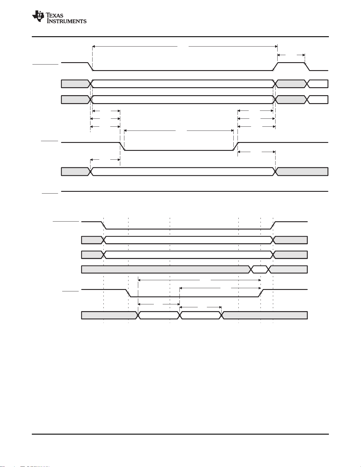
EM_CS[5:2]
EM_BA[1:0]
EM_A[20:0]
EM_WE
EM_D[15:0]
EM_OE
15
1
16
18
20
22
17
19
21
24
25
EM_CS[5:2]
11
Asserted
Deasserted
2
2
EM_BA[1:0]
EM_A[20:0]
EM_D[15:0]
EM_OE
EM_WAITx
SETUP S ROBET ExtendedDuetoEM_WAITx
S ROBET HOLD
14
TMS320C5514
www.ti.com
SPRS646B–AUGUST 2010–REVISED AUGUST 2010
Figure 6-19. Asynchronous Memory Write Timing for EMIF
Figure 6-20. EM_WAITx Read Timing Requirements
Copyright © 2010, Texas Instruments Incorporated Peripheral Information and Electrical Specifications 93
Submit Documentation Feedback
Product Folder Link(s): TMS320C5514
Page 94

EM_CS[5:2]
25
Asserted Deasserted
2
2
EM_BA[1:0]
EM_A[20:0]
EM_D[15:0]
EM_WE
EM_WAITx
SETUP STROBE ExtendedDuetoEM_WAITx STROBE HOLD
28
TMS320C5514
SPRS646B–AUGUST 2010–REVISED AUGUST 2010
Figure 6-21. EM_WAITx Write Timing Requirements
www.ti.com
94 Peripheral Information and Electrical Specifications Copyright © 2010, Texas Instruments Incorporated
Submit Documentation Feedback
Product Folder Link(s): TMS320C5514
Page 95

TMS320C5514
www.ti.com
6.10 Multimedia Card/Secure Digital (MMC/SD)
The device includes two MMC/SD controllers which are compliant with MMC V3.31, Secure Digital Part 1
Physical Layer Specification V2.0, and Secure Digital Input Output (SDIO) V3.3 specifications. The
MMC/SD card controller supports these industry standards and assumes the reader is familiar with these
standards.
Each MMC/SD Controller in the device has the following features:
• Multimedia Card/Secure Digital (MMC/SD) protocol support
• Programmable clock frequency
• 512 bit Read/Write FIFO to lower system overhead
• Slave DMA transfer capability
The MMC/SD card controller transfers data between the CPU and DMA controller on one side and
MMC/SD card on the other side. The CPU and DMA controller can read/write the data in the card by
accessing the registers in the MMC/SD controller.
The MMC/SD controller on this device, does not support the SPI mode of operation.
6.10.1 MMC/SD Peripheral Register Description(s)
Table 6-20 shows the MMC/SD registers. The MMC/SD0 registers start at address 0x3A00 .
SPRS646B–AUGUST 2010–REVISED AUGUST 2010
Copyright © 2010, Texas Instruments Incorporated Peripheral Information and Electrical Specifications 95
Submit Documentation Feedback
Product Folder Link(s): TMS320C5514
Page 96

TMS320C5514
SPRS646B–AUGUST 2010–REVISED AUGUST 2010
Table 6-20. MMC/SD0 Registers
HEX ADDRESS ACRONYM
RANGE
3A00h MMCCTL MMC Control Register
3A04h MMCCLK MMC Memory Clock Control Register
3A08h MMCST0 MMC Status Register 0
3A0Ch MMCST1 MMC Status Register 1
3A10h MMCIM MMC Interrupt Mask Register
3A14h MMCTOR MMC Response Time-Out Register
3A18h MMCTOD MMC Data Read Time-Out Register
3A1Ch MMCBLEN MMC Block Length Register
3A20h MMCNBLK MMC Number of Blocks Register
3A24h MMCNBLC MMC Number of Blocks Counter Register
3A28h MMCDRR1 MMC Data Receive 1 Register
3A29h MMCDRR2 MMC Data Receive 2 Register
3A2Ch MMCDXR1 MMC Data Transmit 1 Register
3A2Dh MMCDXR2 MMC Data Transmit 2 Register
3A30h MMCCMD MMC Command Register
3A34h MMCARGHL MMC Argument Register
3A38h MMCRSP0 MMC Response Register 0
3A39h MMCRSP1 MMC Response Register 1
3A3Ch MMCRSP2 MMC Response Register 2
3A3Dh MMCRSP3 MMC Response Register 3
3A40h MMCRSP4 MMC Response Register 4
3A41h MMCRSP5 MMC Response Register 5
3A44h MMCRSP6 MMC Response Register 6
3A45h MMCRSP7 MMC Response Register 7
3A48h MMCDRSP MMC Data Response Register
3A50h MMCCIDX MMC Command Index Register
3A64h – 3A70h – Reserved
3A74h MMCFIFOCTL MMC FIFO Control Register
www.ti.com
REGISTER NAME
96 Peripheral Information and Electrical Specifications Copyright © 2010, Texas Instruments Incorporated
Submit Documentation Feedback
Product Folder Link(s): TMS320C5514
Page 97

TMS320C5514
www.ti.com
Table 6-21. MMC/SD1 Registers
HEX ADDRESS
RANGE
3B00h MMCCTL MMC Control Register
3B04h MMCCLK MMC Memory Clock Control Register
3B08h MMCST0 MMC Status Register 0
3B0Ch MMCST1 MMC Status Register 1
3B10h MMCIM MMC Interrupt Mask Register
3B14h MMCTOR MMC Response Time-Out Register
3B18h MMCTOD MMC Data Read Time-Out Register
3B1Ch MMCBLEN MMC Block Length Register
3B20h MMCNBLK MMC Number of Blocks Register
3B24h MMCNBLC MMC Number of Blocks Counter Register
3B28h MMCDRR1 MMC Data Receive 1 Register
3B29h MMCDRR2 MMC Data Receive 2 Register
3B2Ch MMCDXR1 MMC Data Transmit 1 Register
3B2Dh MMCDXR2 MMC Data Transmit 2 Register
3B30h MMCCMD MMC Command Register
3B34h MMCARGHL MMC Argument Register
3B38h MMCRSP0 MMC Response Register 0
3B39h MMCRSP1 MMC Response Register 1
3B3Ch MMCRSP2 MMC Response Register 2
3B3Dh MMCRSP3 MMC Response Register 3
3B40h MMCRSP4 MMC Response Register 4
3B41h MMCRSP5 MMC Response Register 5
3B44h MMCRSP6 MMC Response Register 6
3B45h MMCRSP7 MMC Response Register 7
3B48h MMCDRSP MMC Data Response Register
3B50h MMCCIDX MMC Command Index Register
3B74h MMCFIFOCTL MMC FIFO Control Register
ACRONYM REGISTER NAME
SPRS646B–AUGUST 2010–REVISED AUGUST 2010
Copyright © 2010, Texas Instruments Incorporated Peripheral Information and Electrical Specifications 97
Submit Documentation Feedback
Product Folder Link(s): TMS320C5514
Page 98

MMCx_CLK
MMCx_CMD
7
9
10
14
13
VALID
Start
D0 D1 Dx End
7
MMCx_CLK
MMCx_Dx
9
10
4
3 3
4
TMS320C5514
SPRS646B–AUGUST 2010–REVISED AUGUST 2010
6.10.2 MMC/SD Electrical Data/Timing
Table 6-22. Timing Requirements for MMC/SD (see Figure 6-22 and Figure 6-25)
NO
.
1 t
su(CMDV-CLKH)
2 t
h(CLKH-CMDV)
3 t
su(DATV-CLKH)
4 t
h(CLKH-DATV)
Setup time, MMCx_CMD data input valid before MMCx_CLK high 3 3 ns
Hold time, MMCx_CMD data input valid after MMCx_CLK high 3 3 ns
Setup time, MMC_Dx data input valid before MMCx_CLK high 3 3 ns
Hold time, MMC_Dx data input valid after MMCx_CLK high 3 3 ns
Table 6-23. Switching Characteristics Over Recommended Operating Conditions for MMC Output
Figure 6-22 and Figure 6-25)
NO
.
7 f
(CLK)
8 f
(CLK_ID)
9 t
w(CLKL)
10 t
w(CLKH)
11 t
r(CLK)
12 t
f(CLK)
13 t
d(MDCLKL-CMDIV)
14 t
d(MDCLKL-CMDV)
15 t
d(MDCLKL-DATIV)
16 t
d(MDCLKL-DATV)
Operating frequency, MMCx_CLK 0 50
Identification mode frequency, MMCx_CLK 0 400 0 400 kHz
Pulse width, MMCx_CLK low 7 10 ns
Pulse width, MMCx_CLK high 7 10 ns
Rise time, MMCx_CLK 3 3 ns
Fall time, MMCx_CLK 3 3 ns
Delay time, MMCx_CLK low to MMC_CMD data output invalid -4 -4.1 ns
Delay time, MMCx_CLK low to MMC_CMD data output valid 4 5.1 ns
Delay time, MMCx_CLK low to MMC_Dx data output invalid -4 -4.1 ns
Delay time, MMCx_CLK low to MMC_Dx data output valid 4 5.1 ns
(1) For MMC/SD, the parametric values are measured at DV
(2) Use this value or SYS_CLK/2 whichever is smaller.
PARAMETER FAST MODE STD MODE UNIT
= 3.3 V and 2.75 V.
DDIO
CVDD= 1.3 V CVDD= 1.05 V
FAST MODE STD MODE UNIT
MIN MAX MIN MAX
CVDD= 1.3 V CVDD= 1.05 V
MIN MAX MIN MAX
(2)
0 25
www.ti.com
(1)
(see
(2)
MHz
Figure 6-22. MMC/SD Host Command Write Timing
Figure 6-23. MMC/SD Card Response Timing
98 Peripheral Information and Electrical Specifications Copyright © 2010, Texas Instruments Incorporated
Submit Documentation Feedback
Product Folder Link(s): TMS320C5514
Page 99

START XMIT
Valid Valid Valid END
MMCx_CLK
MMCx_CMD
10
9
7
1
2
7 9
10
16
15
MMCx_CLK
MMCx_DAT
VALID
TMS320C5514
www.ti.com
SPRS646B–AUGUST 2010–REVISED AUGUST 2010
Figure 6-24. MMC/SD Host Write Timing
Figure 6-25. MMC/SD Data Write Timing
Copyright © 2010, Texas Instruments Incorporated Peripheral Information and Electrical Specifications 99
Submit Documentation Feedback
Product Folder Link(s): TMS320C5514
Page 100

TMS320C5514
SPRS646B–AUGUST 2010–REVISED AUGUST 2010
6.11 Real-Time Clock (RTC)
The device includes a Real-Time Clock (RTC) with its own separated power supply and isolation circuits.
The separate supply and isolation circuits allow the RTC to run with the least possible power consumption,
called RTC only mode. The RTC only mode requires CV
powered, but other power domains can be shut off. See Section 6.11.1, RTC Only Mode for details. All
RTC registers are preserved (except for RTC Control and RTC Update Registers) and the counter
continues to operate when the device is powered off. The RTC also has the capability to wakeup the
device from idle states via alarms, periodic interrupts, or an external WAKEUP input. Additionally, the RTC
is able to output an alarm or periodic interrupt on the WAKEUP pin to cause external power management
to re-enable power to the DSP Core and I/O. Note: The RTC Core (CV
even though RTC is not used.
The device RTC provides the following features:
• 100-year calendar up to year 2099.
• Counts seconds, minutes, hours, day of the week, date, month, and year with leap year compensation
• Millisecond time correction
• Binary-coded-decimal (BCD) representation of time, calendar, and alarm
• 24-hour clock mode
• Second, minute, hour, day, or week alarm interrupt
• Periodic interrupt: every millisecond, second, minute, hour, or day
• Alarm interrupt: precise time of day
• Single interrupt to the DSP CPU
• 32.768-kHz crystal oscillator with frequency calibration
, LDOI, and DV
DDRTC
power domains to be
DDRTC
) must be powered properly
DDRTC
www.ti.com
Control of the RTC is maintained through a set of I/O memory mapped registers (see Table 6-24). Note
that any write to these registers will be synchronized to the RTC 32.768-KHz clock; thus, the CPU must
run at least 3X faster than the RTC. Writes to these registers will not be evident until the next two
32.768-KHz clock cycles later. Furthermore, if the RTC Oscillator is disabled, no RTC register can be
written to.
The RTC has its own power-on-reset (POR) circuit which resets the registers in the RTC core domain
when power is first applied to the CV
pin nor the digital core's POR (powergood signal).
The scratch registers in the RTC can be used to take advantage of this unique reset domain to keep track
of when the DSP boots and whether the RTC time registers have already been initialized to the current
clock time or whether the software needs to go into a routine to prompt the user to set the time/date.
6.11.1 RTC Only Mode
The maximum power saving can be achieved by using the RTC only mode. There are hardware and
software requirements to use the RTC only mode.
Hardware Requirements:
• The DSP_LDO_EN pin must be tied to GND or pulled down to GND.
• The RTC Core (CV
• VDDA_ANA is recommended to be powered from the ANA_LDOO pin. (In case VDDA_ANA has to be
powered externally, then VDDA_ANA must be always powered, too.)
• All other power domains can be totally shut down during the RTC only mode.
• A high pulse for a minimum of one RTC clock period (30.5 µs) to the WAKEUP pin is required to wake
up the device from the RTC only mode.
), RTC I/O (DV
DDRTC
power pin. The RTC flops are not reset by the device's RESET
DDRTC
), and LDO inputs (LDOI) must be always powered.
DDRTC
100 Peripheral Information and Electrical Specifications Copyright © 2010, Texas Instruments Incorporated
Submit Documentation Feedback
Product Folder Link(s): TMS320C5514
 Loading...