

Page 1

TMS320C3x
User’s Guide
Literature Number: SPRU031E
2558539-9761 revision L
July 1997
Printed on Recycled Paper
Page 2

IMPORTANT NOTICE
T exas Instruments (TI) reserves the right to make changes to its products or to discontinue any
semiconductor product or service without notice, and advises its customers to obtain the latest
version of relevant information to verify , before placing orders, that the information being relied
on is current.
TI warrants performance of its semiconductor products and related software to the specifications
applicable at the time of sale in accordance with TI’s standard warranty . T esting and other quality
control techniques are utilized to the extent TI deems necessary to support this warranty.
Specific testing of all parameters of each device is not necessarily performed, except those
mandated by government requirements.
Certain applications using semiconductor products may involve potential risks of death,
personal injury , or severe property or environmental damage (“Critical Applications”).
TI SEMICONDUCTOR PRODUCTS ARE NOT DESIGNED, INTENDED, AUTHORIZED, OR
WARRANTED TO BE SUITABLE FOR USE IN LIFE-SUPPORT APPLICATIONS, DEVICES
OR SYSTEMS OR OTHER CRITICAL APPLICATIONS.
Inclusion of TI products in such applications is understood to be fully at the risk of the customer.
Use of TI products in such applications requires the written approval of an appropriate TI officer .
Questions concerning potential risk applications should be directed to TI through a local SC
sales office.
In order to minimize risks associated with the customer’s applications, adequate design and
operating safeguards should be provided by the customer to minimize inherent or procedural
hazards.
TI assumes no liability for applications assistance, customer product design, software
performance, or infringement of patents or services described herein. Nor does TI warrant or
represent that any license, either express or implied, is granted under any patent right, copyright,
mask work right, or other intellectual property right of TI covering or relating to any combination,
machine, or process in which such semiconductor products or services might be or are used.
Copyright 1997, Texas Instruments Incorporated
Page 3

About This Manual
Preface
Read This First
This user’s guide serves as an applications reference book for the TMS320C3x
generation of digital signal processors (DSPs). These include the TMS320C30,
TMS320C31, TMS320LC31, and TMS320C32. Throughout the book, all references to ’C3x refer collectively to the ’C30, ’C31, ’LC31 and ’C32.
This book provides information to assist managers and hardware/software
engineers in application development. It includes example code and hardware connections for various applications.
The guide shows how to use the instructions set, the architecture, and the ’C3x
interface. It presents examples for frequently used applications and discusses
more involved examples and applications. It also defines the principles involved
in many applications and gives the corresponding assembly language code for
instructional purposes and for immediate use. Whenever the detailed explanation
of the underlying theory is too extensive to be included in this manual, appropriate
references are given for further information.
Notational Conventions
This document uses the following conventions.
-
Program listings, program examples, and interactive displays are shown in
a special typeface. Examples use a bold version of the special
typeface for emphasis; interactive displays use a bold version of the
special typeface to distinguish commands that you enter from items that the
system displays (such as prompts, command output, error messages, etc.).
Here is a sample program listing:
0011 0005 0001 .field 1, 2
0012 0005 0003 .field 3, 4
0013 0005 0006 .field 6, 3
0014 0006 .even
Here is an example of a system prompt and a command that you might
enter:
C: csr –a /user/ti/simuboard/utilities
iii
Page 4

Notational Conventions
-
In syntax descriptions, the instruction, command, or directive is in bold
typeface and parameters are in an
italic typeface
. Portions of a syntax that
are in bold must be entered as shown; portions of a syntax that are in
describe the type of information that must be entered. Here is an example
of a directive syntax:
italics
.asect ”
The directive .asect has two parameters, indicated by
address
section name
”,
address
section name
. When you use .asect, the first parameter is an actual section
name, enclosed in double quotes; the second parameter is an address.
-
Square brackets ( [ and ] ) identify an optional parameter. If you use an
optional parameter, you specify the information within the brackets; you
do not enter the brackets themselves. Here is an example of an instruction
that has an optional parameter:
LALK
16-bit constant [, shift]
The LALK instruction has two parameters. The first parameter,
constant
, is required. The second parameter,
shift
, is optional. As this syntax
shows, if you use the optional second parameter, you must precede it with a
comma.
Square brackets are also used as part of the pathname specification for
VMS pathnames; in this case, the brackets are actually part of the pathname (they are not optional).
-
Braces ( { and } ) indicate a list. The symbol | (read as or) separates items
within the list. Here is an example of a list:
and
16-bit
{ * | *+ | *– }
This provides three choices: *, *+, or *–.
Unless the list is enclosed in square brackets, you must choose one item
from the list.
-
Some directives can have a varying number of parameters. For example,
the .byte directive can have up to 100 parameters. The syntax for this directive is:
.byte
value1 [, ... , valuen]
This syntax shows that .byte has at least one value parameter, but you
may supply additional value parameters, separated by commas.
iv
Page 5

Information About Cautions / Related Documentation from Texas Instruments
Information About Cautions
This book contains cautions.
This is an example of a caution statement.
A caution statement describes a situation that could potentially
damage your software or equipment.
The information in a caution is provided for your protection. Please read each
caution carefully.
Related Documentation From Texas Instruments
The following books describe the TMS320 floating-point devices and related
support tools. To obtain a copy of any of these TI documents, call the Texas
Instruments Literature Response Center as indicated in the section
Need Assistance
title and literature number.
TMS320C3x General Purpose Applications User’s Guide
SPRU194) provides information to assist you in application development
for the TMS320C3x generation of digital signal processors (DSPs). It
includes example code and hardware connections for various appliances.
It also defines the principles involved in many applications and gives the
corresponding assembly language code for instructional purposes and for
immediate use.
…on page vi. When ordering, please identify the book by its
(literature number
TMS320C3x/C4x Assembly Language Tools User’s Guide
number SPRU035) describes the assembly language tools (assembler,
linker, and other tools used to develop assembly language code),
assembler directives, macros, common object file format, and symbolic
debugging directives for the ’C3x and ’C4x generations of devices.
TMS320C3x/C4x Optimizing C Compiler User’s Guide
SPRU034) describes the TMS320 floating-point C compiler. This C compiler
accepts ANSI standard C source code and produces TMS320 assembly
language source code for the ’C3x and ’C4x generations of devices.
(literature number
If You
(literature
Read This First
v
Page 6

Related Documentation from Texas Instruments / References
References
TMS320C3x C Source Debugger User’s Guide
(literature number
SPRU053) tells you how to invoke the ’C3x emulator , evaluation module,
and simulator versions of the C source debugger interface. This book
discusses various aspects of the debugger interface, including window
management, command entry , code execution, data management, and
breakpoints. It also includes a tutorial that introduces basic debugger
functionality.
TMS320 DSP Development Support Reference Guide
(literature number
SPRU011) describes the TMS320 family of digital signal processors and
the tools that support these devices. Included are code-generation tools
(compilers, assemblers, linkers, etc.) and system integration and debug
tools (simulators, emulators, evaluation modules, etc.). Also covered are
available documentation, seminars, the university program, and factory
repair and exchange.
TMS320 Third-Party Support Reference Guide
(literature number
SPRU052) alphabetically lists over 100 third parties that provide various
products that serve the family of TMS320 digital signal processors. A
myriad of products and applications are offered—software and hardware
development tools, speech recognition, image processing, noise cancellation, modems, etc.
The publications in the following reference list contain useful information
regarding functions, operations, and applications of digital signal processing
(DSP). These books also provide other references to many useful technical
papers. The reference list is organized into categories of general DSP , speech,
image processing, and digital control theory and is alphabetized by author.
-
General Digital Signal Processing
Antoniou, Andreas,
Digital Filters: Analysis and Design
. New York, NY:
McGraw-Hill Company, Inc., 1979.
Bateman, A., and Y ates, W.,
Digital Signal Processing Design
. Salt Lake
City, Utah: W. H. Freeman and Company, 1990.
Brigham, E. Oran,
The Fast Fourier Transform.
Englewood Cliffs, NJ:
Prentice-Hall, Inc., 1974.
Burrus, C.S., and Parks, T .W .,
DFT/FFT and Convolution Algorithms.
New
York, NY: John Wiley and Sons, Inc., 1984.
Chassaing, R., and Horning, D.,
TMS320C25.
New York, NY: John Wiley and Sons, Inc., 1990.
Digital Signal Processing Applications with the TMS320 Family , Vol. I.
Digital Signal Processing with the
Tex-
as Instruments, 1986; Prentice-Hall, Inc., 1987.
vi
Page 7

References
Digital Signal Processing Applications with the TMS320 Family, Vol. III.
Texas Instruments, 1990; Prentice-Hall, Inc., 1990.
Gold, Bernard, and Rader, C.M.
NY: McGraw-Hill Company, Inc., 1969.
Hamming, R.W.,
1977.
Hutchins, B., and Parks, T.,
the TMS320C25
IEEE ASSP DSP Committee (Editor),
New York, NY: IEEE Press, 1979.
Jackson, Leland B.,
Kluwer Academic Publishers, 1986.
Jones, D.L., and Parks, T.W .,
the TMS32010.
Lim, Jae, and Oppenheim, Alan V. (Editors),
Processing
Morris, L. Robert,
Carleton University, 1983.
Oppenheim, Alan V. (Editor),
Englewood Cliffs, NJ: Prentice-Hall, Inc., 1978.
Oppenheim, Alan V ., and Schafer, R.W .,
wood Cliffs, NJ: Prentice-Hall, Inc., 1975.
Oppenheim, Alan V ., and Schafer, R.W .,
Englewood Cliffs, NJ: Prentice-Hall, Inc., 1989.
Oppenheim, Alan V., and Willsky, A.N., with Young, I.T.,
Systems.
Parks, T .W., and Burrus, C.S.,
and Sons, Inc., 1987.
Rabiner, Lawrence R., and Gold, Bernard,
Signal Processing
Treichler , J.R., Johnson, Jr., C.R., and Larimore, M.G.,
of Adaptive Filters
Digital Filters
. Englewood Cliffs, NJ: Prentice-Hall, Inc., 1990.
Digital Filters and Signal Processing.
Englewood Cliffs, NJ: Prentice-Hall, Inc., 1987.
. Englewood Cliffs, NJ: Prentice-Hall, Inc., 1988.
Digital Signal Processing Software.
Englewood Cliffs, NJ: Prentice-Hall, Inc., 1983.
. Englewood Cliffs, NJ: Prentice-Hall, Inc., 1975.
. New York, NY: John Wiley and Sons, Inc., 1987.
, Digital Processing of Signals.
. Englewood Cliffs, NJ: Prentice-Hall, Inc.,
New Y ork,
A Digital Signal Processing Laboratory Using
Programs for Digital Signal Processing.
Hingham, MA:
A Digital Signal Processing Laboratory Using
Advanced Topics in Signal
Ottawa, Canada:
Applications of Digital Signal Processing.
Digital Signal Processing.
Engle-
Discrete-Time Signal Processing.
Signals and
Digital Filter Design.
New Y or k, NY : John Wi ley
Theory and Application of Digital
Theory and Design
-
Speech
Gray , A.H., and Markel, J.D.,
Springer-Verlag, 1976.
Jayant, N.S., and Noll, Peter,
Cliffs, NJ: Prentice-Hall, Inc., 1984.
Papamichalis, Panos,
wood Cliffs, NJ: Prentice-Hall, Inc., 1987.
Linear Prediction of Speech
Digital Coding of Waveforms
Practical Approaches to Speech Coding.
. New Y ork, NY :
Read This First
. Englewood
Engle-
vii
Page 8

References
Parsons, Thomas.,
Voice and Speech Processing.
McGraw Hill Company, Inc., 1987.
Rabiner, Lawrence R., and Schafer, R.W.,
Signals.
Shaughnessy , Douglas.,
Englewood Cliffs, NJ: Prentice-Hall, Inc., 1978.
Speech Communication.
Digital Processing of Speech
Wesley, 1987.
-
Image Processing
Andrews, H.C., and Hunt, B.R.,
Digital Image Restoration
Cliffs, NJ: Prentice-Hall, Inc., 1977.
Gonzales, Rafael C., and Wintz, Paul,
Digital Image Processing.
MA: Addison-Wesley Publishing Company, Inc., 1977.
Pratt, William K.,
Digital Image Processing
. New Y ork, NY: John Wiley and
Sons, 1978.
-
Multirate DSP
Crochiere, R.E., and Rabiner, L.R.,
Multirate Digital Signal Processing
Englewood Cliffs, NJ: Prentice-Hall, Inc., 1983.
V aidyanathan, P .P .,
Multirate Systems and Filter Banks
NJ: Prentice-Hall, Inc.
-
Digital Control Theory
New York, NY:
Reading, MA: Addison-
. Englewood
Reading,
.
. Englewood Cliffs,
viii
Dote, Y .,
Servo Motor and Motion Control Using Digital Signal Processors
.
Englewood Cliffs, NJ: Prentice-Hall, Inc., 1990.
Jacquot, R.,
Modern Digital Control Systems.
New Y ork, NY: Marcel Dekker,
Inc., 1981.
Katz, P.,
Digital Control Using Microprocessors
. Englewood Cliffs, NJ:
Prentice-Hall, Inc., 1981.
Kuo, B.C.,
Digital Control Systems.
New York, NY: Holt, Reinholt and
Winston, Inc., 1980.
Moroney , P .,
tors.
Cambridge, MA: The MIT Press, 1983.
Phillips, C., and Nagle, H.,
Issues in the Implementation of Digital Feedback Compensa-
Digital Control System Analysis and Design.
Englewood Cliffs, NJ: Prentice-Hall, Inc., 1984.
-
Adaptive Signal Processing
Haykin, S.,
Adaptive Filter Theory.
Englewood Cliffs, NJ: Prentice-Hall,
Inc., 1991.
Widrow, B., and Stearns, S.D.
Adaptive Signal Processing.
Englewood
Cliffs, NJ: Prentice-Hall, Inc., 1985.
Page 9

-
Array Signal Processing
References
Haykin, S., Justice, J.H., Owsley, N.L., Y en, J.L., and Kak, A.C.
Processing.
Hudson, J.E.
Englewood Cliffs, NJ: Prentice-Hall, Inc., 1985.
Adaptive Array Principles.
New York, NY: John Wiley and
Sons, 1981.
Monzingo, R.A., and Miller, J.W.
Introduction to Adaptive Arrays.
NY: John Wiley and Sons, 1980.
Array Signal
New Y or k,
Read This First
ix
Page 10
If You Need Assistance
If You Need Assistance . . .
-
World-Wide Web Sites
TI Online http://www.ti.com
Semiconductor Product Information Center (PIC) http://www.ti.com/sc/docs/pic/home.htm
DSP Solutions http://www.ti.com/dsps
320 Hotline On-line
Microcontroller Home Page http://www.ti.com/sc/micro
Networking Home Page http://www.ti.com/sc/docs/network/nbuhomex.htm
-
North America, South America, Central America
Product Information Center (PIC) (972) 644-5580
TI Literature Response Center U.S.A. (800) 477-8924
Software Registration/Upgrades (214) 638-0333 Fax: (214) 638-7742
U.S.A. Factory Repair/Hardware Upgrades (281) 274-2285
U.S. Technical Training Organization (972) 644-5580
Microcontroller Hotline (281) 274-2370 Fax: (281) 274-4203 Email: mi cro @ti.com
Microcontroller Modem BBS (281) 274-3700 8-N-1
DSP Hotline (281) 274-2320 Fax: (281) 274-2324 Email: dsph@ti.com
DSP Modem BBS (281) 274-2323
DSP Internet BBS via anonymous ftp to ftp://ftp.ti.com/pub/tms320bbs
Networking Hotline Fax: (281) 274-4027
-
Europe, Middle East, Africa
European Product Information Center (EPIC) Hotlines:
Multi-Language Support +33 1 30 70 11 69 Fax: +33 1 30 70 10 32 Email: epic@ti.com
Deutsch +49 8161 80 33 11 or +33 1 30 70 11 68
English +33 1 30 70 11 65
Francais +33 1 30 70 11 64
Italiano +33 1 30 70 11 67
EPIC Modem BBS +33 1 30 70 11 99
European Factory Repair +33 4 93 22 25 40
Europe Customer Training Helpline Fax: +49 81 61 80 40 10
-
Asia-Pacific
Literature Response Center +852 2 956 7288 Fax: +852 2 956 2200
Hong Kong DSP Hotline +852 2 956 7268 Fax: +852 2 956 1002
Korea DSP Hotline +82 2 551 2804 Fax: +82 2 551 2828
Korea DSP Modem BBS +82 2 551 2914
Singapore DSP Hotline Fax: +65 390 7179
Taiwan DSP Hotline +886 2 377 1450 Fax: +886 2 377 2718
Taiwan DSP Modem BBS +886 2 376 2592
Taiwan DSP Internet BBS via anonymous ftp to ftp://dsp.ee.tit.edu.tw/pub/TI/
-
Japan
Product Information Center +0120-81-0026 (in Japan) Fax: +0120-81-0036 (in Japan)
DSP Hotline +03-3769-8735 or (INTL) 813-3769-8735 Fax: +03-3457-7071 or (INTL) 813-3457-7071
DSP BBS via Nifty-Serve Type “Go TIASP”
t
+03-3457-0972 or (INTL) 813-3457-0972 Fax: +03-3457-1259 or (INTL) 813-3457-1259
http://www.ti.com/sc/docs/dsps/support.htm
Email: TLANHOT@micro.ti.com
x
Page 11

If You Need Assistance / Trademarks
-
Documentation
When making suggestions or reporting errors in documentation, please include the following information that is on the title
page: the full title of the book, the publication date, and the literature number.
Mail: Texas Instruments Incorporated Email: comments@books.sc.ti.com
Technical Documentation Services, MS 702
P.O. Box 1443
Houston, Texas 77251-1443
Note: When calling a Literature Response Center to order documentation, please specify the literature number of the
book.
Trademarks
ABEL is a trademark of DATA I/O.
CodeView, MS, MS-DOS, MS-Windows, and Presentation Manager are registered trademarks of
Microsoft Corporation.
DEC, Digital DX, Ultrix, VAX, and VMS are trademarks of Digital Equipment Corporation.
HPGL is registered trademark of Hewlett Packard Company.
Macintosh and MPW are trademarks of Apple Computer Corp.
Micro Channel, OS/2, PC-DOS, and PGA are trademarks of International Business Machines Corporation.
SP ARC, Sun 3, Sun 4, Sun Workstation, SunView, and SunWindows are trademark of SP ARC International,
Inc., but licensed exclusively to Sun Microsystems, Inc.
UNIX is a registered trademark in the United States and other countries, licensed exclusively through
X/Open Company Limited.
Read This First
xi
Page 12

Contents
Contents
1 Introduction 1-1. . . . . . . . . . . . . . . . . . . . . . . . . . . . . . . . . . . . . . . . . . . . . . . . . . . . . . . . . . . . . . . . . . . . .
A general description of the TMS320C30, TMS320C31, and TMS320C32, their key features,
and typical applications.
1.1 TMS320C3x Devices 1-2. . . . . . . . . . . . . . . . . . . . . . . . . . . . . . . . . . . . . . . . . . . . . . . . . . . . . . . .
1.1.1 TMS320C3x Key Specifications 1-3. . . . . . . . . . . . . . . . . . . . . . . . . . . . . . . . . . . . . . .
1.1.2 TMS320C30 1-3. . . . . . . . . . . . . . . . . . . . . . . . . . . . . . . . . . . . . . . . . . . . . . . . . . . . . . . .
1.1.3 TMS320C31 and TMS320LC31 1-3. . . . . . . . . . . . . . . . . . . . . . . . . . . . . . . . . . . . . . .
1.1.4 TMS320C32 1-4. . . . . . . . . . . . . . . . . . . . . . . . . . . . . . . . . . . . . . . . . . . . . . . . . . . . . . . .
1.2 Typical Applications 1-7. . . . . . . . . . . . . . . . . . . . . . . . . . . . . . . . . . . . . . . . . . . . . . . . . . . . . . . . .
2 Architectural Overview 2-1. . . . . . . . . . . . . . . . . . . . . . . . . . . . . . . . . . . . . . . . . . . . . . . . . . . . . . . . . . .
Functional block diagram, ’C3x design description, hardware components, device operation,
and instruction set summary.
2.1 Overview 2-2. . . . . . . . . . . . . . . . . . . . . . . . . . . . . . . . . . . . . . . . . . . . . . . . . . . . . . . . . . . . . . . . . .
2.2 Central Processing Unit (CPU) 2-6. . . . . . . . . . . . . . . . . . . . . . . . . . . . . . . . . . . . . . . . . . . . . . .
2.2.1 Floating-Point/Integer Multiplier 2-8. . . . . . . . . . . . . . . . . . . . . . . . . . . . . . . . . . . . . . .
2.2.2 Arithmetic Logic Unit (ALU) and Internal Buses 2-8. . . . . . . . . . . . . . . . . . . . . . . . . .
2.2.3 Auxiliary Register Arithmetic Units (ARAUs) 2-8. . . . . . . . . . . . . . . . . . . . . . . . . . . . .
2.3 CPU Primary Register File 2-9. . . . . . . . . . . . . . . . . . . . . . . . . . . . . . . . . . . . . . . . . . . . . . . . . . .
2.4 Other Registers 2-12. . . . . . . . . . . . . . . . . . . . . . . . . . . . . . . . . . . . . . . . . . . . . . . . . . . . . . . . . . .
2.5 Memory Organization 2-13. . . . . . . . . . . . . . . . . . . . . . . . . . . . . . . . . . . . . . . . . . . . . . . . . . . . . .
2.5.1 RAM, ROM, and Cache 2-13. . . . . . . . . . . . . . . . . . . . . . . . . . . . . . . . . . . . . . . . . . . . .
2.5.2 Memory Addressing Modes 2-17. . . . . . . . . . . . . . . . . . . . . . . . . . . . . . . . . . . . . . . . . .
2.6 Internal Bus Operation 2-18. . . . . . . . . . . . . . . . . . . . . . . . . . . . . . . . . . . . . . . . . . . . . . . . . . . . .
2.7 External Memory Interface 2-19. . . . . . . . . . . . . . . . . . . . . . . . . . . . . . . . . . . . . . . . . . . . . . . . . .
2.7.1 TMS320C32 16- and 32-Bit Program Memory 2-19. . . . . . . . . . . . . . . . . . . . . . . . . .
2.7.2 TMS320C32 8-, 16-, and 32-Bit Data Memory 2-20. . . . . . . . . . . . . . . . . . . . . . . . . .
2.8 Interrupts 2-21. . . . . . . . . . . . . . . . . . . . . . . . . . . . . . . . . . . . . . . . . . . . . . . . . . . . . . . . . . . . . . . . .
2.9 Peripherals 2-22. . . . . . . . . . . . . . . . . . . . . . . . . . . . . . . . . . . . . . . . . . . . . . . . . . . . . . . . . . . . . . .
2.9.1 Timers 2-23. . . . . . . . . . . . . . . . . . . . . . . . . . . . . . . . . . . . . . . . . . . . . . . . . . . . . . . . . . . .
2.9.2 Serial Ports 2-23. . . . . . . . . . . . . . . . . . . . . . . . . . . . . . . . . . . . . . . . . . . . . . . . . . . . . . . .
2.10 Direct Memory Access (DMA) 2-24. . . . . . . . . . . . . . . . . . . . . . . . . . . . . . . . . . . . . . . . . . . . . . .
2.11 TMS320C30, TMS320C31, and TMS320C32 Differences 2-26. . . . . . . . . . . . . . . . . . . . . . .
xiii
Page 13

Contents
3 CPU Registers 3-1. . . . . . . . . . . . . . . . . . . . . . . . . . . . . . . . . . . . . . . . . . . . . . . . . . . . . . . . . . . . . . . . . . .
Description of the registers in the CPU register file.
3.1 CPU Multiport Register File 3-2. . . . . . . . . . . . . . . . . . . . . . . . . . . . . . . . . . . . . . . . . . . . . . . . . .
3.1.1 Extended-Precision Registers (R7–R0) 3-3. . . . . . . . . . . . . . . . . . . . . . . . . . . . . . . . .
3.1.2 Auxiliary Registers (AR7–AR0) 3-4. . . . . . . . . . . . . . . . . . . . . . . . . . . . . . . . . . . . . . . .
3.1.3 Data-Page Pointer (DP) 3-4. . . . . . . . . . . . . . . . . . . . . . . . . . . . . . . . . . . . . . . . . . . . . .
3.1.4 Index Registers (IR0, IR1) 3-4. . . . . . . . . . . . . . . . . . . . . . . . . . . . . . . . . . . . . . . . . . . .
3.1.5 Block Size (BK) Register 3-4. . . . . . . . . . . . . . . . . . . . . . . . . . . . . . . . . . . . . . . . . . . . .
3.1.6 System-Stack Pointer (SP) 3-4. . . . . . . . . . . . . . . . . . . . . . . . . . . . . . . . . . . . . . . . . . .
3.1.7 Status (ST) Register 3-5. . . . . . . . . . . . . . . . . . . . . . . . . . . . . . . . . . . . . . . . . . . . . . . . .
3.1.8 CPU/DMA Interrupt-Enable (IE) Register 3-9. . . . . . . . . . . . . . . . . . . . . . . . . . . . . . .
3.1.9 CPU Interrupt Flag (IF) Register 3-11. . . . . . . . . . . . . . . . . . . . . . . . . . . . . . . . . . . . . .
3.1.10 I/O Flag (IOF) Register 3-16. . . . . . . . . . . . . . . . . . . . . . . . . . . . . . . . . . . . . . . . . . . . . .
3.1.11 Repeat-Counter (RC) and Block-Repeat (RS, RE) Registers 3-17. . . . . . . . . . . . .
3.2 Other Registers 3-18. . . . . . . . . . . . . . . . . . . . . . . . . . . . . . . . . . . . . . . . . . . . . . . . . . . . . . . . . . .
3.2.1 Program-Counter (PC) Register 3-18. . . . . . . . . . . . . . . . . . . . . . . . . . . . . . . . . . . . . .
3.2.2 Instruction Register (IR) 3-18. . . . . . . . . . . . . . . . . . . . . . . . . . . . . . . . . . . . . . . . . . . . .
3.3 Reserved Bits and Compatibility 3-19. . . . . . . . . . . . . . . . . . . . . . . . . . . . . . . . . . . . . . . . . . . . .
4 Memory and the Instruction Cache 4-1. . . . . . . . . . . . . . . . . . . . . . . . . . . . . . . . . . . . . . . . . . . . . . . .
Description of memory maps with explanation of instruction cache architecture, algorithm,
and control bits.
4.1 Memory 4-2. . . . . . . . . . . . . . . . . . . . . . . . . . . . . . . . . . . . . . . . . . . . . . . . . . . . . . . . . . . . . . . . . . .
4.1.1 Memory Maps 4-2. . . . . . . . . . . . . . . . . . . . . . . . . . . . . . . . . . . . . . . . . . . . . . . . . . . . . . .
4.1.2 Peripheral Bus Memory Map 4-9. . . . . . . . . . . . . . . . . . . . . . . . . . . . . . . . . . . . . . . . . .
4.2 Reset/Interrupt/Trap Vector Map 4-14. . . . . . . . . . . . . . . . . . . . . . . . . . . . . . . . . . . . . . . . . . . . .
4.3 Instruction Cache 4-19. . . . . . . . . . . . . . . . . . . . . . . . . . . . . . . . . . . . . . . . . . . . . . . . . . . . . . . . . .
4.3.1 Instruction-Cache Architecture 4-19. . . . . . . . . . . . . . . . . . . . . . . . . . . . . . . . . . . . . . .
4.3.2 Instruction-Cache Algorithm 4-21. . . . . . . . . . . . . . . . . . . . . . . . . . . . . . . . . . . . . . . . . .
4.3.3 Cache Control Bits 4-22. . . . . . . . . . . . . . . . . . . . . . . . . . . . . . . . . . . . . . . . . . . . . . . . . .
5 Data Formats and Floating-Point Operation 5-1. . . . . . . . . . . . . . . . . . . . . . . . . . . . . . . . . . . . . . .
Description of signed and unsigned integer and floating-point formats. Discussion of floatingpoint multiplication, addition, subtraction, normalization, rounding, and conversions.
5.1 Integer Formats 5-2. . . . . . . . . . . . . . . . . . . . . . . . . . . . . . . . . . . . . . . . . . . . . . . . . . . . . . . . . . . .
5.1.1 Short-Integer Format 5-2. . . . . . . . . . . . . . . . . . . . . . . . . . . . . . . . . . . . . . . . . . . . . . . . .
5.1.2 Single-Precision Integer Format 5-2. . . . . . . . . . . . . . . . . . . . . . . . . . . . . . . . . . . . . . .
5.2 Unsigned-Integer Formats 5-3. . . . . . . . . . . . . . . . . . . . . . . . . . . . . . . . . . . . . . . . . . . . . . . . . . .
5.2.1 Short Unsigned-Integer Format 5-3. . . . . . . . . . . . . . . . . . . . . . . . . . . . . . . . . . . . . . . .
5.2.2 Single-Precision Unsigned-Integer Format 5-3. . . . . . . . . . . . . . . . . . . . . . . . . . . . . .
5.3 Floating-Point Formats 5-4. . . . . . . . . . . . . . . . . . . . . . . . . . . . . . . . . . . . . . . . . . . . . . . . . . . . . .
5.3.1 Short Floating-Point Format 5-5. . . . . . . . . . . . . . . . . . . . . . . . . . . . . . . . . . . . . . . . . . .
5.3.2 TMS320C32 Short Floating-Point Format for External 16-Bit Data 5-6. . . . . . . . .
xiv
Page 14

Contents
5.3.3 Single-Precision Floating-Point Format 5-7. . . . . . . . . . . . . . . . . . . . . . . . . . . . . . . . .
5.3.4 Extended-Precision Floating-Point Format 5-8. . . . . . . . . . . . . . . . . . . . . . . . . . . . . .
5.3.5 Determining the Decimal Equivalent of a TMS320C3x
Floating-Point Format 5-9. . . . . . . . . . . . . . . . . . . . . . . . . . . . . . . . . . . . . . . . . . . . . . . .
5.3.6 Conversion Between Floating-Point Formats 5-12. . . . . . . . . . . . . . . . . . . . . . . . . . .
5.4 Floating-Point Conversion (IEEE Std. 754) 5-14. . . . . . . . . . . . . . . . . . . . . . . . . . . . . . . . . . . .
5.4.1 Converting IEEE Format to 2s-Complement TMS320C3x
Floating-Point Format 5-15. . . . . . . . . . . . . . . . . . . . . . . . . . . . . . . . . . . . . . . . . . . . . . .
5.4.2 Converting 2s-Complement TMS320C3x Floating-Point Format
to IEEE Format 5-21. . . . . . . . . . . . . . . . . . . . . . . . . . . . . . . . . . . . . . . . . . . . . . . . . . . . .
5.5 Floating-Point Multiplication 5-26. . . . . . . . . . . . . . . . . . . . . . . . . . . . . . . . . . . . . . . . . . . . . . . . .
5.6 Floating-Point Addition and Subtraction 5-32. . . . . . . . . . . . . . . . . . . . . . . . . . . . . . . . . . . . . . .
5.7 Normalization Using the NORM Instruction 5-37. . . . . . . . . . . . . . . . . . . . . . . . . . . . . . . . . . . .
5.8 Rounding (RND Instruction) 5-39. . . . . . . . . . . . . . . . . . . . . . . . . . . . . . . . . . . . . . . . . . . . . . . . .
5.9 Floating-Point to Integer Conversion (FIX Instruction) 5-41. . . . . . . . . . . . . . . . . . . . . . . . . . .
5.10 Integer to Floating-Point Conversion (FLOAT Instruction) 5-43. . . . . . . . . . . . . . . . . . . . . . .
5.11 Fast Logarithms on a Floating-Point Device 5-44. . . . . . . . . . . . . . . . . . . . . . . . . . . . . . . . . . .
5.11.1 Example of Fast Logarithm on a Floating-Point Device 5-45. . . . . . . . . . . . . . . . . .
5.11.2 Points to Consider 5-47. . . . . . . . . . . . . . . . . . . . . . . . . . . . . . . . . . . . . . . . . . . . . . . . . .
6 Addressing Modes 6-1. . . . . . . . . . . . . . . . . . . . . . . . . . . . . . . . . . . . . . . . . . . . . . . . . . . . . . . . . . . . . .
Operation, encoding, and implementation of addressing modes; format descriptions;
system stack management.
6.1 Addressing Types 6-2. . . . . . . . . . . . . . . . . . . . . . . . . . . . . . . . . . . . . . . . . . . . . . . . . . . . . . . . . .
6.2 Register Addressing 6-3. . . . . . . . . . . . . . . . . . . . . . . . . . . . . . . . . . . . . . . . . . . . . . . . . . . . . . . .
6.3 Direct Addressing 6-4. . . . . . . . . . . . . . . . . . . . . . . . . . . . . . . . . . . . . . . . . . . . . . . . . . . . . . . . . . .
6.4 Indirect Addressing 6-5. . . . . . . . . . . . . . . . . . . . . . . . . . . . . . . . . . . . . . . . . . . . . . . . . . . . . . . . .
6.5 Immediate Addressing 6-18. . . . . . . . . . . . . . . . . . . . . . . . . . . . . . . . . . . . . . . . . . . . . . . . . . . . .
6.6 PC-Relative Addressing 6-19. . . . . . . . . . . . . . . . . . . . . . . . . . . . . . . . . . . . . . . . . . . . . . . . . . . .
6.7 Circular Addressing 6-21. . . . . . . . . . . . . . . . . . . . . . . . . . . . . . . . . . . . . . . . . . . . . . . . . . . . . . . .
6.8 Bit-Reversed Addressing 6-26. . . . . . . . . . . . . . . . . . . . . . . . . . . . . . . . . . . . . . . . . . . . . . . . . . .
6.9 Aligning Buffers With the TMS320 Floating-Point DSP Assembly Language Tools 6-28. . . .
6.10 System and User Stack Management 6-29. . . . . . . . . . . . . . . . . . . . . . . . . . . . . . . . . . . . . . . .
6.10.1 System-Stack Pointer 6-29. . . . . . . . . . . . . . . . . . . . . . . . . . . . . . . . . . . . . . . . . . . . . . .
6.10.2 Stacks 6-30. . . . . . . . . . . . . . . . . . . . . . . . . . . . . . . . . . . . . . . . . . . . . . . . . . . . . . . . . . . .
6.10.3 Queues 6-31. . . . . . . . . . . . . . . . . . . . . . . . . . . . . . . . . . . . . . . . . . . . . . . . . . . . . . . . . . .
7 Program Flow Control 7-1. . . . . . . . . . . . . . . . . . . . . . . . . . . . . . . . . . . . . . . . . . . . . . . . . . . . . . . . . . .
Software control of program flow with repeat modes and branching; interlocked operations;
reset and interrupts.
7.1 Repeat Modes 7-2. . . . . . . . . . . . . . . . . . . . . . . . . . . . . . . . . . . . . . . . . . . . . . . . . . . . . . . . . . . . .
7.1.1 Repeat-Mode Control Bits 7-3. . . . . . . . . . . . . . . . . . . . . . . . . . . . . . . . . . . . . . . . . . . .
7.1.2 Repeat-Mode Operation 7-3. . . . . . . . . . . . . . . . . . . . . . . . . . . . . . . . . . . . . . . . . . . . . .
7.1.3 RPTB Instruction 7-4. . . . . . . . . . . . . . . . . . . . . . . . . . . . . . . . . . . . . . . . . . . . . . . . . . . .
Contents
xv
Page 15

Contents
7.1.4 RPTS Instruction 7-5. . . . . . . . . . . . . . . . . . . . . . . . . . . . . . . . . . . . . . . . . . . . . . . . . . . .
7.1.5 Repeat-Mode Restrictions 7-6. . . . . . . . . . . . . . . . . . . . . . . . . . . . . . . . . . . . . . . . . . . .
7.1.6 RC Register Value After Repeat Mode Completes 7-7. . . . . . . . . . . . . . . . . . . . . . .
7.1.7 Nested Block Repeats 7-8. . . . . . . . . . . . . . . . . . . . . . . . . . . . . . . . . . . . . . . . . . . . . . .
7.2 Delayed Branches 7-9. . . . . . . . . . . . . . . . . . . . . . . . . . . . . . . . . . . . . . . . . . . . . . . . . . . . . . . . . .
7.3 Calls, Traps, and Returns 7-11. . . . . . . . . . . . . . . . . . . . . . . . . . . . . . . . . . . . . . . . . . . . . . . . . . .
7.4 Interlocked Operations 7-13. . . . . . . . . . . . . . . . . . . . . . . . . . . . . . . . . . . . . . . . . . . . . . . . . . . . .
7.4.1 Interrupting Interlocked Operations 7-15. . . . . . . . . . . . . . . . . . . . . . . . . . . . . . . . . . .
7.4.2 Using Interlocked Operations 7-15. . . . . . . . . . . . . . . . . . . . . . . . . . . . . . . . . . . . . . . .
7.4.3 Pipeline Effects of Interlocked Instructions 7-19. . . . . . . . . . . . . . . . . . . . . . . . . . . . .
7.5 Reset Operation 7-21. . . . . . . . . . . . . . . . . . . . . . . . . . . . . . . . . . . . . . . . . . . . . . . . . . . . . . . . . . .
7.6 Interrupts 7-26. . . . . . . . . . . . . . . . . . . . . . . . . . . . . . . . . . . . . . . . . . . . . . . . . . . . . . . . . . . . . . . . .
7.6.1 TMS320C30 and TMS320C31 Interrupt Vector Table 7-26. . . . . . . . . . . . . . . . . . . .
7.6.2 TMS320C32 Interrupt Vector Table 7-29. . . . . . . . . . . . . . . . . . . . . . . . . . . . . . . . . . .
7.6.3 Interrupt Prioritization 7-31. . . . . . . . . . . . . . . . . . . . . . . . . . . . . . . . . . . . . . . . . . . . . . .
7.6.4 CPU Interrupt Control Bits 7-32. . . . . . . . . . . . . . . . . . . . . . . . . . . . . . . . . . . . . . . . . . .
7.6.5 Interrupt Flag Register Behavior 7-32. . . . . . . . . . . . . . . . . . . . . . . . . . . . . . . . . . . . . .
7.6.6 Interrupt Processing 7-33. . . . . . . . . . . . . . . . . . . . . . . . . . . . . . . . . . . . . . . . . . . . . . . .
7.6.7 CPU Interrupt Latency 7-35. . . . . . . . . . . . . . . . . . . . . . . . . . . . . . . . . . . . . . . . . . . . . .
7.6.8 External Interrupts 7-36. . . . . . . . . . . . . . . . . . . . . . . . . . . . . . . . . . . . . . . . . . . . . . . . . .
7.7 DMA Interrupts 7-38. . . . . . . . . . . . . . . . . . . . . . . . . . . . . . . . . . . . . . . . . . . . . . . . . . . . . . . . . . . .
7.7.1 DMA Interrupt Control Bits 7-38. . . . . . . . . . . . . . . . . . . . . . . . . . . . . . . . . . . . . . . . . . .
7.7.2 DMA Interrupt Processing 7-39. . . . . . . . . . . . . . . . . . . . . . . . . . . . . . . . . . . . . . . . . . .
7.7.3 CPU/DMA Interaction 7-40. . . . . . . . . . . . . . . . . . . . . . . . . . . . . . . . . . . . . . . . . . . . . . .
7.7.4 TMS320C3x Interrupt Considerations 7-41. . . . . . . . . . . . . . . . . . . . . . . . . . . . . . . . .
7.7.5 TMS320C30 Interrupt Considerations 7-44. . . . . . . . . . . . . . . . . . . . . . . . . . . . . . . . .
7.8 Traps 7-47. . . . . . . . . . . . . . . . . . . . . . . . . . . . . . . . . . . . . . . . . . . . . . . . . . . . . . . . . . . . . . . . . . . .
7.8.1 Initialization of Traps and Interrupts 7-47. . . . . . . . . . . . . . . . . . . . . . . . . . . . . . . . . . .
7.8.2 Operation of Traps 7-47. . . . . . . . . . . . . . . . . . . . . . . . . . . . . . . . . . . . . . . . . . . . . . . . . .
7.9 Power Management Modes 7-49. . . . . . . . . . . . . . . . . . . . . . . . . . . . . . . . . . . . . . . . . . . . . . . . .
7.9.1 IDLE2 Power-Down Mode 7-49. . . . . . . . . . . . . . . . . . . . . . . . . . . . . . . . . . . . . . . . . . .
7.9.2 LOPOWER 7-51. . . . . . . . . . . . . . . . . . . . . . . . . . . . . . . . . . . . . . . . . . . . . . . . . . . . . . . .
8 Pipeline Operation 8-1. . . . . . . . . . . . . . . . . . . . . . . . . . . . . . . . . . . . . . . . . . . . . . . . . . . . . . . . . . . . . . .
Discussion of the pipeline of operations on the TMS320C3x
8.1 Pipeline Structure 8-2. . . . . . . . . . . . . . . . . . . . . . . . . . . . . . . . . . . . . . . . . . . . . . . . . . . . . . . . . . .
8.2 Pipeline Conflicts 8-4. . . . . . . . . . . . . . . . . . . . . . . . . . . . . . . . . . . . . . . . . . . . . . . . . . . . . . . . . . .
8.2.1 Branch Conflicts 8-4. . . . . . . . . . . . . . . . . . . . . . . . . . . . . . . . . . . . . . . . . . . . . . . . . . . . .
8.2.2 Register Conflicts 8-6. . . . . . . . . . . . . . . . . . . . . . . . . . . . . . . . . . . . . . . . . . . . . . . . . . . .
8.2.3 Memory Conflicts 8-8. . . . . . . . . . . . . . . . . . . . . . . . . . . . . . . . . . . . . . . . . . . . . . . . . . . .
8.3 Resolving Register Conflicts 8-19. . . . . . . . . . . . . . . . . . . . . . . . . . . . . . . . . . . . . . . . . . . . . . . .
8.4 Memory Access for Maximum Performance 8-22. . . . . . . . . . . . . . . . . . . . . . . . . . . . . . . . . . .
8.5 Clocking Memory Accesses 8-24. . . . . . . . . . . . . . . . . . . . . . . . . . . . . . . . . . . . . . . . . . . . . . . . .
8.5.1 Program Fetches 8-24. . . . . . . . . . . . . . . . . . . . . . . . . . . . . . . . . . . . . . . . . . . . . . . . . . .
8.5.2 Data Loads and Stores 8-24. . . . . . . . . . . . . . . . . . . . . . . . . . . . . . . . . . . . . . . . . . . . . .
xvi
Page 16

Contents
9 TMS320C30 and TMS320C31 External-Memory Interface 9-1. . . . . . . . . . . . . . . . . . . . . . . . . . . .
Description of primary and expansion interfaces for the ’C30 and ’C31; external interface timing
diagrams; programmable wait-states and bank switching.
9.1 Overview 9-2. . . . . . . . . . . . . . . . . . . . . . . . . . . . . . . . . . . . . . . . . . . . . . . . . . . . . . . . . . . . . . . . . .
9.2 Memory Interface Signals 9-3. . . . . . . . . . . . . . . . . . . . . . . . . . . . . . . . . . . . . . . . . . . . . . . . . . . .
9.2.1 TMS320C30 Memory Interface Signals 9-3. . . . . . . . . . . . . . . . . . . . . . . . . . . . . . . .
9.2.2 TMS320C31 Memory Interface Signals 9-3. . . . . . . . . . . . . . . . . . . . . . . . . . . . . . . .
9.3 Memory Interface Control Registers 9-7. . . . . . . . . . . . . . . . . . . . . . . . . . . . . . . . . . . . . . . . . . .
9.3.1 Primary-Bus Control Register 9-7. . . . . . . . . . . . . . . . . . . . . . . . . . . . . . . . . . . . . . . .
9.3.2 Expansion-Bus Control Register 9-9. . . . . . . . . . . . . . . . . . . . . . . . . . . . . . . . . . . . . .
9.4 Programmable Wait States 9-10. . . . . . . . . . . . . . . . . . . . . . . . . . . . . . . . . . . . . . . . . . . . . . . . . .
9.5 Programmable Bank Switching 9-12. . . . . . . . . . . . . . . . . . . . . . . . . . . . . . . . . . . . . . . . . . . . . .
9.6 External Memory Interface Timing 9-15. . . . . . . . . . . . . . . . . . . . . . . . . . . . . . . . . . . . . . . . . . .
9.6.1 Primary-Bus Cycles 9-15. . . . . . . . . . . . . . . . . . . . . . . . . . . . . . . . . . . . . . . . . . . . . . .
9.6.2 Expansion-Bus I/O Cycles 9-21. . . . . . . . . . . . . . . . . . . . . . . . . . . . . . . . . . . . . . . . . .
9.6.3 Hold Cycles 9-37. . . . . . . . . . . . . . . . . . . . . . . . . . . . . . . . . . . . . . . . . . . . . . . . . . . . . .
10 TMS320C32 Enhanced External Memory Interface 10-1. . . . . . . . . . . . . . . . . . . . . . . . . . . . . . . .
Description of primary and expansion interfaces for the ’C32; external interface timing
diagrams; programmable wait-states and bank switching.
10.1 TMS320C32 Memory Features 10-2. . . . . . . . . . . . . . . . . . . . . . . . . . . . . . . . . . . . . . . . . . . . . .
10.2 TMS320C32 Memory Overview 10-3. . . . . . . . . . . . . . . . . . . . . . . . . . . . . . . . . . . . . . . . . . . . .
10.2.1 External Memory Interface Overview 10-3. . . . . . . . . . . . . . . . . . . . . . . . . . . . . . . . .
10.2.2 Program Memory Access 10-4. . . . . . . . . . . . . . . . . . . . . . . . . . . . . . . . . . . . . . . . . . .
10.2.3 Data Memory Access 10-5. . . . . . . . . . . . . . . . . . . . . . . . . . . . . . . . . . . . . . . . . . . . . .
10.3 Configuration 10-7. . . . . . . . . . . . . . . . . . . . . . . . . . . . . . . . . . . . . . . . . . . . . . . . . . . . . . . . . . . . .
10.3.1 External Interface Control Registers 10-7. . . . . . . . . . . . . . . . . . . . . . . . . . . . . . . . .
10.3.2 Using Physical Memory Width and Data-Type Size Fields 10-13. . . . . . . . . . . . .
10.4 Programmable Wait States 10-15. . . . . . . . . . . . . . . . . . . . . . . . . . . . . . . . . . . . . . . . . . . . . . . . .
10.5 Programmable Bank Switching 10-17. . . . . . . . . . . . . . . . . . . . . . . . . . . . . . . . . . . . . . . . . . . . .
10.6 32-Bit-Wide Memory Interface 10-20. . . . . . . . . . . . . . . . . . . . . . . . . . . . . . . . . . . . . . . . . . . . . .
10.7 16-Bit-Wide Memory Interface 10-26. . . . . . . . . . . . . . . . . . . . . . . . . . . . . . . . . . . . . . . . . . . . . .
10.8 8-Bit-Wide Memory Interface 10-32. . . . . . . . . . . . . . . . . . . . . . . . . . . . . . . . . . . . . . . . . . . . . . .
10.9 External Ready Timing Improvement 10-38. . . . . . . . . . . . . . . . . . . . . . . . . . . . . . . . . . . . . . . .
10.10 Bus Timing 10-39. . . . . . . . . . . . . . . . . . . . . . . . . . . . . . . . . . . . . . . . . . . . . . . . . . . . . . . . . . . . . .
10.10.1 STRB0
10.10.2 IOSTRB
and STRB1 Bus Cycles 10-39. . . . . . . . . . . . . . . . . . . . . . . . . . . . . . . . . . . .
Bus Cycles 10-42. . . . . . . . . . . . . . . . . . . . . . . . . . . . . . . . . . . . . . . . . . . . . .
10.10.3 Inactive Bus States 10-51. . . . . . . . . . . . . . . . . . . . . . . . . . . . . . . . . . . . . . . . . . . . . . .
11 Using the TMS320C31 and TMS320C32 Boot Loaders 11-1. . . . . . . . . . . . . . . . . . . . . . . . . . . . .
Description of the boot loader operations for the ’C31 and ’C32.
11.1 TMS320C31 Boot Loader 11-2. . . . . . . . . . . . . . . . . . . . . . . . . . . . . . . . . . . . . . . . . . . . . . . . . . .
11.1.1 TMS320C31 Boot-Loader Description 11-2. . . . . . . . . . . . . . . . . . . . . . . . . . . . . . . .
11.1.2 TMS320C31 Boot-Loader Mode Selection 11-2. . . . . . . . . . . . . . . . . . . . . . . . . . . .
Contents
xvii
Page 17

Contents
11.1.3 TMS320C31 Boot-Loading Sequence 11-4. . . . . . . . . . . . . . . . . . . . . . . . . . . . . . . .
11.1.4 TMS320C31 Boot Data Stream Structure 11-7. . . . . . . . . . . . . . . . . . . . . . . . . . . . .
11.1.5 Interrupt and Trap-Vector Mapping 11-11. . . . . . . . . . . . . . . . . . . . . . . . . . . . . . . . .
11.1.6 TMS320C31 Boot-Loader Precautions 11-13. . . . . . . . . . . . . . . . . . . . . . . . . . . . . .
11.2 TMS320C32 Boot Loader 11-14. . . . . . . . . . . . . . . . . . . . . . . . . . . . . . . . . . . . . . . . . . . . . . . . . .
11.2.1 TMS320C32 Boot-Loader Description 11-14. . . . . . . . . . . . . . . . . . . . . . . . . . . . . . .
11.2.2 TMS320C32 Boot-Loader Mode Selection 11-14. . . . . . . . . . . . . . . . . . . . . . . . . . .
11.2.3 TMS320C32 Boot-Loading Sequence 11-15. . . . . . . . . . . . . . . . . . . . . . . . . . . . . . .
11.2.4 TMS320C32 Boot Data Stream Structure 11-20. . . . . . . . . . . . . . . . . . . . . . . . . . . .
11.2.5 Boot-Loader Hardware Interface 11-23. . . . . . . . . . . . . . . . . . . . . . . . . . . . . . . . . . .
11.2.6 TMS320C32 Boot-Loader Precautions 11-23. . . . . . . . . . . . . . . . . . . . . . . . . . . . . .
12 Peripherals 12-1. . . . . . . . . . . . . . . . . . . . . . . . . . . . . . . . . . . . . . . . . . . . . . . . . . . . . . . . . . . . . . . . . . . . .
Description of the DMA controller, timers, and serial ports.
12.1 Timers 12-2. . . . . . . . . . . . . . . . . . . . . . . . . . . . . . . . . . . . . . . . . . . . . . . . . . . . . . . . . . . . . . . . . . .
12.1.1 Timer Pins 12-3. . . . . . . . . . . . . . . . . . . . . . . . . . . . . . . . . . . . . . . . . . . . . . . . . . . . . . . .
12.1.2 Timer Control Registers 12-3. . . . . . . . . . . . . . . . . . . . . . . . . . . . . . . . . . . . . . . . . . . .
12.1.3 Timer Global-Control Register 12-4. . . . . . . . . . . . . . . . . . . . . . . . . . . . . . . . . . . . . .
12.1.4 Timer-Period and Counter Registers 12-7. . . . . . . . . . . . . . . . . . . . . . . . . . . . . . . . .
12.1.5 Timer Pulse Generation 12-7. . . . . . . . . . . . . . . . . . . . . . . . . . . . . . . . . . . . . . . . . . . .
12.1.6 Timer Operation Modes 12-10. . . . . . . . . . . . . . . . . . . . . . . . . . . . . . . . . . . . . . . . . . .
12.1.7 Using TCLKx as General-Purpose I/O Pins 12-12. . . . . . . . . . . . . . . . . . . . . . . . . .
12.1.8 Timer Interrupts 12-13. . . . . . . . . . . . . . . . . . . . . . . . . . . . . . . . . . . . . . . . . . . . . . . . . .
12.1.9 Timer Initialization/Reconfiguration 12-13. . . . . . . . . . . . . . . . . . . . . . . . . . . . . . . . .
12.2 Serial Ports 12-15. . . . . . . . . . . . . . . . . . . . . . . . . . . . . . . . . . . . . . . . . . . . . . . . . . . . . . . . . . . . . .
12.2.1 Serial-Port Global-Control Register 12-17. . . . . . . . . . . . . . . . . . . . . . . . . . . . . . . . .
12.2.2 FSX/DX/CLKX Port-Control Register 12-22. . . . . . . . . . . . . . . . . . . . . . . . . . . . . . . .
12.2.3 FSR/DR/CLKR Port-Control Register 12-23. . . . . . . . . . . . . . . . . . . . . . . . . . . . . . .
12.2.4 Receive/Transmit Timer-Control Register 12-25. . . . . . . . . . . . . . . . . . . . . . . . . . . .
12.2.5 Receive/Transmit Timer-Counter Register 12-27. . . . . . . . . . . . . . . . . . . . . . . . . . .
12.2.6 Receive/Transmit Timer-Period Register 12-28. . . . . . . . . . . . . . . . . . . . . . . . . . . .
12.2.7 Data-Transmit Register 12-28. . . . . . . . . . . . . . . . . . . . . . . . . . . . . . . . . . . . . . . . . . .
12.2.8 Data-Receive Register 12-28. . . . . . . . . . . . . . . . . . . . . . . . . . . . . . . . . . . . . . . . . . . .
12.2.9 Serial-Port Operation Configurations 12-29. . . . . . . . . . . . . . . . . . . . . . . . . . . . . . . .
12.2.10 Serial-Port Timing 12-31. . . . . . . . . . . . . . . . . . . . . . . . . . . . . . . . . . . . . . . . . . . . . . . .
12.2.11 Serial-Port Interrupt Sources 12-34. . . . . . . . . . . . . . . . . . . . . . . . . . . . . . . . . . . . . . .
12.2.12 Serial-Port Functional Operation 12-35. . . . . . . . . . . . . . . . . . . . . . . . . . . . . . . . . . .
12.2.13 Serial-Port Initialization/Reconfiguration 12-41. . . . . . . . . . . . . . . . . . . . . . . . . . . . .
12.2.14 TMS320C3x Serial-Port Interface Examples 12-41. . . . . . . . . . . . . . . . . . . . . . . . .
12.3 DMA Controller 12-48. . . . . . . . . . . . . . . . . . . . . . . . . . . . . . . . . . . . . . . . . . . . . . . . . . . . . . . . . . .
12.3.1 DMA Functional Description 12-48. . . . . . . . . . . . . . . . . . . . . . . . . . . . . . . . . . . . . . .
12.3.2 DMA Basic Operation 12-50. . . . . . . . . . . . . . . . . . . . . . . . . . . . . . . . . . . . . . . . . . . . .
12.3.3 DMA Registers 12-51. . . . . . . . . . . . . . . . . . . . . . . . . . . . . . . . . . . . . . . . . . . . . . . . . . .
12.3.4 CPU/DMA Interrupt-Enable Register 12-59. . . . . . . . . . . . . . . . . . . . . . . . . . . . . . . .
xviii
Page 18

Contents
12.3.5 TMS320C32 DMA Internal Priority Schemes 12-62. . . . . . . . . . . . . . . . . . . . . . . . .
12.3.6 CPU and DMA Controller Arbitration 12-63. . . . . . . . . . . . . . . . . . . . . . . . . . . . . . . .
12.3.7 DMA and Interrupts 12-64. . . . . . . . . . . . . . . . . . . . . . . . . . . . . . . . . . . . . . . . . . . . . . .
12.3.8 DMA Memory Transfer Timing 12-67. . . . . . . . . . . . . . . . . . . . . . . . . . . . . . . . . . . . .
12.3.9 DMA Initialization/Reconfiguration 12-73. . . . . . . . . . . . . . . . . . . . . . . . . . . . . . . . . .
12.3.10 Hints for DMA Programming 12-73. . . . . . . . . . . . . . . . . . . . . . . . . . . . . . . . . . . . . . .
12.3.11 DMA Programming Examples 12-74. . . . . . . . . . . . . . . . . . . . . . . . . . . . . . . . . . . . . .
13 Assembly Language Instructions 13-1. . . . . . . . . . . . . . . . . . . . . . . . . . . . . . . . . . . . . . . . . . . . . . . .
Functional listing of instructions. Condition codes defined. Alphabetized individual instruction
set with examples.
13.1 Instruction Set 13-2. . . . . . . . . . . . . . . . . . . . . . . . . . . . . . . . . . . . . . . . . . . . . . . . . . . . . . . . . . . . .
13.1.1 Load and Store Instructions 13-2. . . . . . . . . . . . . . . . . . . . . . . . . . . . . . . . . . . . . . . . .
13.1.2 2-Operand Instructions 13-3. . . . . . . . . . . . . . . . . . . . . . . . . . . . . . . . . . . . . . . . . . . . .
13.1.3 3-Operand Instructions 13-4. . . . . . . . . . . . . . . . . . . . . . . . . . . . . . . . . . . . . . . . . . . . .
13.1.4 Program-Control Instructions 13-4. . . . . . . . . . . . . . . . . . . . . . . . . . . . . . . . . . . . . . .
13.1.5 Low-Power Control Instructions 13-5. . . . . . . . . . . . . . . . . . . . . . . . . . . . . . . . . . . . .
13.1.6 Interlocked-Operations Instructions 13-5. . . . . . . . . . . . . . . . . . . . . . . . . . . . . . . . . .
13.1.7 Parallel-Operations Instructions 13-6. . . . . . . . . . . . . . . . . . . . . . . . . . . . . . . . . . . . .
13.1.8 Illegal Instructions 13-9. . . . . . . . . . . . . . . . . . . . . . . . . . . . . . . . . . . . . . . . . . . . . . . . .
13.2 Instruction Set Summary 13-10. . . . . . . . . . . . . . . . . . . . . . . . . . . . . . . . . . . . . . . . . . . . . . . . . .
13.3 Parallel Instruction Set Summary 13-17. . . . . . . . . . . . . . . . . . . . . . . . . . . . . . . . . . . . . . . . . . .
13.4 Group Addressing Mode Instruction Encoding 13-20. . . . . . . . . . . . . . . . . . . . . . . . . . . . . . . .
13.4.1 General Addressing Modes 13-20. . . . . . . . . . . . . . . . . . . . . . . . . . . . . . . . . . . . . . . .
13.4.2 3-Operand Addressing Modes 13-24. . . . . . . . . . . . . . . . . . . . . . . . . . . . . . . . . . . . .
13.4.3 Parallel Addressing Modes 13-25. . . . . . . . . . . . . . . . . . . . . . . . . . . . . . . . . . . . . . . .
13.4.4 Conditional-Branch Addressing Modes 13-27. . . . . . . . . . . . . . . . . . . . . . . . . . . . . .
13.5 Condition Codes and Flags 13-28. . . . . . . . . . . . . . . . . . . . . . . . . . . . . . . . . . . . . . . . . . . . . . . .
13.6 Individual Instructions 13-32. . . . . . . . . . . . . . . . . . . . . . . . . . . . . . . . . . . . . . . . . . . . . . . . . . . . .
13.6.1 Symbols and Abbreviations 13-32. . . . . . . . . . . . . . . . . . . . . . . . . . . . . . . . . . . . . . . .
13.6.2 Optional Assembler Syntax 13-34. . . . . . . . . . . . . . . . . . . . . . . . . . . . . . . . . . . . . . . .
13.6.3 Individual Instruction Descriptions 13-37. . . . . . . . . . . . . . . . . . . . . . . . . . . . . . . . . .
A Instruction Opcodes A-1. . . . . . . . . . . . . . . . . . . . . . . . . . . . . . . . . . . . . . . . . . . . . . . . . . . . . . . . . . . . .
List of the opcode fields for the TMS320C3x instructions.
B TMS320C31 Boot Loader Source Code B-1. . . . . . . . . . . . . . . . . . . . . . . . . . . . . . . . . . . . . . . . . . . .
C TMS320C32 Boot Loader Source Code C-1. . . . . . . . . . . . . . . . . . . . . . . . . . . . . . . . . . . . . . . . . . . .
C.1 Boot-Loader Source Code Description C-2. . . . . . . . . . . . . . . . . . . . . . . . . . . . . . . . . . . . . . . . .
C.2 Boot-Loader Source Code Listing C-4. . . . . . . . . . . . . . . . . . . . . . . . . . . . . . . . . . . . . . . . . . . . .
D Glossary D-1. . . . . . . . . . . . . . . . . . . . . . . . . . . . . . . . . . . . . . . . . . . . . . . . . . . . . . . . . . . . . . . . . . . . . . . .
Contents
xix
Page 19

Figures
Figures
1–1 TMS320C3x Devices Block Diagram 1-3. . . . . . . . . . . . . . . . . . . . . . . . . . . . . . . . . . . . . . . . . . . .
2–1 TMS320C30 Block Diagram 2-3. . . . . . . . . . . . . . . . . . . . . . . . . . . . . . . . . . . . . . . . . . . . . . . . . . . .
2–2 TMS320C31 Block Diagram 2-4. . . . . . . . . . . . . . . . . . . . . . . . . . . . . . . . . . . . . . . . . . . . . . . . . . . .
2–3 TMS320C32 Block Diagram 2-5. . . . . . . . . . . . . . . . . . . . . . . . . . . . . . . . . . . . . . . . . . . . . . . . . . . .
2–4 Central Processing Unit (CPU) 2-7. . . . . . . . . . . . . . . . . . . . . . . . . . . . . . . . . . . . . . . . . . . . . . . . . .
2–5 Memory Organization of the TMS320C30 2-14. . . . . . . . . . . . . . . . . . . . . . . . . . . . . . . . . . . . . . .
2–6 Memory Organization of the TMS320C31 2-15. . . . . . . . . . . . . . . . . . . . . . . . . . . . . . . . . . . . . . .
2–7 Memory Organization of the TMS320C32 2-16. . . . . . . . . . . . . . . . . . . . . . . . . . . . . . . . . . . . . . .
2–8 TMS320C32-Supported Data Types and Sizes and External Memory Widths 2-20. . . . . . . .
2–9 Peripheral Modules 2-22. . . . . . . . . . . . . . . . . . . . . . . . . . . . . . . . . . . . . . . . . . . . . . . . . . . . . . . . . . .
2–10 DMA Controller 2-25. . . . . . . . . . . . . . . . . . . . . . . . . . . . . . . . . . . . . . . . . . . . . . . . . . . . . . . . . . . . . .
3–1 Extended-Precision Register Floating-Point Format 3-3. . . . . . . . . . . . . . . . . . . . . . . . . . . . . . . .
3–2 Extended-Precision Register Integer Format 3-3. . . . . . . . . . . . . . . . . . . . . . . . . . . . . . . . . . . . . .
3–3 Status Register (TMS320C30 andTMS320C31) 3-5. . . . . . . . . . . . . . . . . . . . . . . . . . . . . . . . . . .
3–4 Status Register (TMS320C32 Only) 3-5. . . . . . . . . . . . . . . . . . . . . . . . . . . . . . . . . . . . . . . . . . . . .
3–5 CPU/DMA Interrupt-Enable (IE) Register (TMS320C30 and TMS320C31) 3-9. . . . . . . . . . .
3–6 CPU/DMA Interrupt-Enable (IE) Register (TMS320C32) 3-9. . . . . . . . . . . . . . . . . . . . . . . . . . . .
3–7 TMS320C30 CPU Interrupt Flag (IF) Register 3-12. . . . . . . . . . . . . . . . . . . . . . . . . . . . . . . . . . . .
3–8 TMS320C31 CPU Interrupt Flag (IF) Register 3-12. . . . . . . . . . . . . . . . . . . . . . . . . . . . . . . . . . . .
3–9 TMS320C32 CPU Interrupt Flag (IF) Register 3-12. . . . . . . . . . . . . . . . . . . . . . . . . . . . . . . . . . . .
3–10 Effective Base Address of the Interrupt-Trap Vector Table 3-14. . . . . . . . . . . . . . . . . . . . . . . . .
3–11 Interrupt and Trap Vector Locations 3-15. . . . . . . . . . . . . . . . . . . . . . . . . . . . . . . . . . . . . . . . . . . .
3–12 I/O Flag (IOF) Register 3-16. . . . . . . . . . . . . . . . . . . . . . . . . . . . . . . . . . . . . . . . . . . . . . . . . . . . . . .
4–1 TMS320C30 Memory Maps 4-4. . . . . . . . . . . . . . . . . . . . . . . . . . . . . . . . . . . . . . . . . . . . . . . . . . . .
4–2 TMS320C31 Memory Maps 4-6. . . . . . . . . . . . . . . . . . . . . . . . . . . . . . . . . . . . . . . . . . . . . . . . . . . .
4–3 TMS320C32 Memory Maps 4-8. . . . . . . . . . . . . . . . . . . . . . . . . . . . . . . . . . . . . . . . . . . . . . . . . . . .
4–4 TMS320C30 Peripheral Bus Memory-Mapped Registers 4-10. . . . . . . . . . . . . . . . . . . . . . . . . .
4–5 TMS320C31 Peripheral Bus Memory-Mapped Registers 4-11. . . . . . . . . . . . . . . . . . . . . . . . . .
4–6 TMS320C32 Peripheral Bus Memory-Mapped Registers 4-13. . . . . . . . . . . . . . . . . . . . . . . . . .
4–7 Reset, Interrupt, and Trap Vector Locations for the TMS320C30
4–8 Reset, Interrupt, and Trap Vector Locations for theTMS320C31
4–9 Interrupt and Trap Branch Instructions for the TMS320C31 Microcomputer Mode 4-17. . . . .
4–10 Interrupt and Trap Vector Locations for TMS320C32 4-18. . . . . . . . . . . . . . . . . . . . . . . . . . . . . .
4–11 Address Partitioning for Cache Control Algorithm 4-19. . . . . . . . . . . . . . . . . . . . . . . . . . . . . . . . .
4–12 Instruction-Cache Architecture 4-20. . . . . . . . . . . . . . . . . . . . . . . . . . . . . . . . . . . . . . . . . . . . . . . . .
Microprocessor Mode 4-15. . . . . . . . . . . . . . . . . . . . . . . . . . . . . . . . . . . . . . . . . . . . . . . . . . . . . . . . .
Microprocessor Mode 4-16. . . . . . . . . . . . . . . . . . . . . . . . . . . . . . . . . . . . . . . . . . . . . . . . . . . . . . . . .
xx
Page 20

Figures
5–1 Short-Integer Format and Sign-Extension of Short Integers 5-2. . . . . . . . . . . . . . . . . . . . . . . . .
5–2 Single-Precision Integer Format 5-2. . . . . . . . . . . . . . . . . . . . . . . . . . . . . . . . . . . . . . . . . . . . . . . . .
5–3 Short Unsigned-Integer Format and Zero Fill 5-3. . . . . . . . . . . . . . . . . . . . . . . . . . . . . . . . . . . . .
5–4 Single-Precision Unsigned-Integer Format 5-3. . . . . . . . . . . . . . . . . . . . . . . . . . . . . . . . . . . . . . . .
5–5 General Floating-Point Format 5-4. . . . . . . . . . . . . . . . . . . . . . . . . . . . . . . . . . . . . . . . . . . . . . . . . .
5–6 Short Floating-Point Format 5-5. . . . . . . . . . . . . . . . . . . . . . . . . . . . . . . . . . . . . . . . . . . . . . . . . . . .
5–7 TMS320C32 Short Floating-Point Format for External 16-Bit Data 5-6. . . . . . . . . . . . . . . . . . .
5–8 Single-Precision Floating-Point Format 5-7. . . . . . . . . . . . . . . . . . . . . . . . . . . . . . . . . . . . . . . . . . .
5–9 Extended-Precision Floating-Point Format 5-8. . . . . . . . . . . . . . . . . . . . . . . . . . . . . . . . . . . . . . . .
5–10 Converting from Short Floating-Point Format to Single-Precision
Floating-Point Format 5-12. . . . . . . . . . . . . . . . . . . . . . . . . . . . . . . . . . . . . . . . . . . . . . . . . . . . . . . . .
5–11 Converting from Short Floating-Point Format to Extended-Precision
Floating-Point Format 5-12. . . . . . . . . . . . . . . . . . . . . . . . . . . . . . . . . . . . . . . . . . . . . . . . . . . . . . . . .
5–12 Converting from Single-Precision Floating-Point Format to Extended-Precision
Floating-Point Format 5-13. . . . . . . . . . . . . . . . . . . . . . . . . . . . . . . . . . . . . . . . . . . . . . . . . . . . . . . . .
5–13 Converting from Extended-Precision Floating-Point Format to Single-Precision
Floating-Point Format 5-13. . . . . . . . . . . . . . . . . . . . . . . . . . . . . . . . . . . . . . . . . . . . . . . . . . . . . . . . .
5–14 IEEE Single-Precision Std. 754 Floating-Point Format 5-14. . . . . . . . . . . . . . . . . . . . . . . . . . . .
5–15 TMS320C3x Single-Precision 2s-Complement Floating-Point Format 5-15. . . . . . . . . . . . . . .
5–16 Flowchart for Floating-Point Multiplication 5-28. . . . . . . . . . . . . . . . . . . . . . . . . . . . . . . . . . . . . . .
5–17 Flowchart for Floating-Point Addition 5-33. . . . . . . . . . . . . . . . . . . . . . . . . . . . . . . . . . . . . . . . . . . .
5–18 Flowchart for NORM Instruction Operation 5-38. . . . . . . . . . . . . . . . . . . . . . . . . . . . . . . . . . . . . .
5–19 Flowchart for Floating-Point Rounding by the RND Instruction 5-40. . . . . . . . . . . . . . . . . . . . .
5–20 Flowchart for Floating-Point to Integer Conversion by FIX Instruction 5-42. . . . . . . . . . . . . . .
5–21 Flowchart for Integer to Floating-Point Conversion by FLOAT Instruction 5-43. . . . . . . . . . . .
5–22 Tabulated Values for Mantissa 5-46. . . . . . . . . . . . . . . . . . . . . . . . . . . . . . . . . . . . . . . . . . . . . . . . .
5–23 Fast Logarithm for FFT Displays 5-48. . . . . . . . . . . . . . . . . . . . . . . . . . . . . . . . . . . . . . . . . . . . . . .
6–1 Direct Addressing 6-4. . . . . . . . . . . . . . . . . . . . . . . . . . . . . . . . . . . . . . . . . . . . . . . . . . . . . . . . . . . . .
6–2 Indirect Addressing Operand Encoding 6-6. . . . . . . . . . . . . . . . . . . . . . . . . . . . . . . . . . . . . . . . . .
6–3 Encoding for 24-Bit PC-Relative Addressing Mode 6-20. . . . . . . . . . . . . . . . . . . . . . . . . . . . . . .
6–4 Logical and Physical Representation of Circular Buffer 6-21. . . . . . . . . . . . . . . . . . . . . . . . . . . .
6–5 Logical and Physical Representation of Circular Buffer after Writing Three Values 6-21. . . .
6–6 Logical and Physical Representation of Circular Buffer after Writing Eight Values 6-22. . . . .
6–7 Circular Buffer Implementation 6-23. . . . . . . . . . . . . . . . . . . . . . . . . . . . . . . . . . . . . . . . . . . . . . . . .
6–8 Data Structure for FIR Filters 6-24. . . . . . . . . . . . . . . . . . . . . . . . . . . . . . . . . . . . . . . . . . . . . . . . . .
6–9 System Stack Configuration 6-29. . . . . . . . . . . . . . . . . . . . . . . . . . . . . . . . . . . . . . . . . . . . . . . . . . .
6–10 Implementations of High-to-Low Memory Stacks 6-30. . . . . . . . . . . . . . . . . . . . . . . . . . . . . . . . .
6–11 Implementations of Low-to-High Memory Stacks 6-31. . . . . . . . . . . . . . . . . . . . . . . . . . . . . . . . .
7–1 CALL Response Timing 7-12. . . . . . . . . . . . . . . . . . . . . . . . . . . . . . . . . . . . . . . . . . . . . . . . . . . . . . .
7–2 Multiple TMS320C3xs Sharing Global Memory 7-17. . . . . . . . . . . . . . . . . . . . . . . . . . . . . . . . . . .
7–3 Zero-Logic Interconnect of TMS320C3x Devices 7-18. . . . . . . . . . . . . . . . . . . . . . . . . . . . . . . . .
7–4 Effective Base Address of the Interrupt-Trap-Vector Table 7-29. . . . . . . . . . . . . . . . . . . . . . . . .
7–5 IF Register Modification 7-33. . . . . . . . . . . . . . . . . . . . . . . . . . . . . . . . . . . . . . . . . . . . . . . . . . . . . . .
7–6 CPU Interrupt Processing 7-34. . . . . . . . . . . . . . . . . . . . . . . . . . . . . . . . . . . . . . . . . . . . . . . . . . . . .
7–7 Interrupt Logic Functional Diagram 7-37. . . . . . . . . . . . . . . . . . . . . . . . . . . . . . . . . . . . . . . . . . . . .
Contents
xxi
Page 21

Figures
7–8 DMA Interrupt Processing 7-39. . . . . . . . . . . . . . . . . . . . . . . . . . . . . . . . . . . . . . . . . . . . . . . . . . . . .
7–9 Parallel CPU and DMA Interrupt Processing 7-40. . . . . . . . . . . . . . . . . . . . . . . . . . . . . . . . . . . . .
7–10 Flow of Traps 7-47. . . . . . . . . . . . . . . . . . . . . . . . . . . . . . . . . . . . . . . . . . . . . . . . . . . . . . . . . . . . . . . .
7–11 IDLE2 Timing 7-50. . . . . . . . . . . . . . . . . . . . . . . . . . . . . . . . . . . . . . . . . . . . . . . . . . . . . . . . . . . . . . . .
7–12 Interrupt Response Timing After IDLE2 Operation 7-51. . . . . . . . . . . . . . . . . . . . . . . . . . . . . . . .
7–13 LOPOWER Timing 7-52. . . . . . . . . . . . . . . . . . . . . . . . . . . . . . . . . . . . . . . . . . . . . . . . . . . . . . . . . . .
7–14 MAXSPEED Timing 7-52. . . . . . . . . . . . . . . . . . . . . . . . . . . . . . . . . . . . . . . . . . . . . . . . . . . . . . . . . .
8–1 TMS320C3x Pipeline Structure 8-2. . . . . . . . . . . . . . . . . . . . . . . . . . . . . . . . . . . . . . . . . . . . . . . . .
8–2 Minor Clock Periods 8-24. . . . . . . . . . . . . . . . . . . . . . . . . . . . . . . . . . . . . . . . . . . . . . . . . . . . . . . . . .
8–3 2-Operand Instruction Word 8-25. . . . . . . . . . . . . . . . . . . . . . . . . . . . . . . . . . . . . . . . . . . . . . . . . . .
8–4 3-Operand Instruction Word 8-25. . . . . . . . . . . . . . . . . . . . . . . . . . . . . . . . . . . . . . . . . . . . . . . . . . .
8–5 Multiply or CPU Operation With a Parallel Store 8-29. . . . . . . . . . . . . . . . . . . . . . . . . . . . . . . . . .
8–6 Two Parallel Stores 8-29. . . . . . . . . . . . . . . . . . . . . . . . . . . . . . . . . . . . . . . . . . . . . . . . . . . . . . . . . . .
8–7 Parallel Multiplies and Adds 8-30. . . . . . . . . . . . . . . . . . . . . . . . . . . . . . . . . . . . . . . . . . . . . . . . . . .
9–1 Memory-Mapped External Interface Control Registers 9-6. . . . . . . . . . . . . . . . . . . . . . . . . . . . .
9–2 Primary-Bus Control Register 9-7. . . . . . . . . . . . . . . . . . . . . . . . . . . . . . . . . . . . . . . . . . . . . . . . . . .
9–3 Expansion-Bus Control Register 9-9. . . . . . . . . . . . . . . . . . . . . . . . . . . . . . . . . . . . . . . . . . . . . . . .
9–4 BNKCMP Example 9-12. . . . . . . . . . . . . . . . . . . . . . . . . . . . . . . . . . . . . . . . . . . . . . . . . . . . . . . . . . .
9–5 Bank-Switching Example 9-14. . . . . . . . . . . . . . . . . . . . . . . . . . . . . . . . . . . . . . . . . . . . . . . . . . . . . .
9–6 Read-Read-Write for (M)STRB
= 0 9-17. . . . . . . . . . . . . . . . . . . . . . . . . . . . . . . . . . . . . . . . . . . . .
9–7 Write-Write-Read for (M)STRB = 0 9-18. . . . . . . . . . . . . . . . . . . . . . . . . . . . . . . . . . . . . . . . . . . . .
9–8 Use of Wait States for Read for (M)STRB = 0 9-19. . . . . . . . . . . . . . . . . . . . . . . . . . . . . . . . . . . .
9–9 Use of Wait States for Write for (M)STRB = 0 9-20. . . . . . . . . . . . . . . . . . . . . . . . . . . . . . . . . . . .
9–10 Read and Write for IOSTRB
= 0 9-21. . . . . . . . . . . . . . . . . . . . . . . . . . . . . . . . . . . . . . . . . . . . . . . .
9–11 Read With One Wait State for IOSTRB = 0 9-22. . . . . . . . . . . . . . . . . . . . . . . . . . . . . . . . . . . . . .
9–12 Write With One Wait State for IOSTRB = 0 9-23. . . . . . . . . . . . . . . . . . . . . . . . . . . . . . . . . . . . . .
9–13 Memory Read and I/O Write for Expansion Bus 9-24. . . . . . . . . . . . . . . . . . . . . . . . . . . . . . . . . .
9–14 Memory Read and I/O Read for Expansion Bus 9-25. . . . . . . . . . . . . . . . . . . . . . . . . . . . . . . . . .
9–15 Memory Write and I/O Write for Expansion Bus 9-26. . . . . . . . . . . . . . . . . . . . . . . . . . . . . . . . . .
9–16 Memory Write and I/O Read for Expansion Bus 9-27. . . . . . . . . . . . . . . . . . . . . . . . . . . . . . . . . .
9–17 I/O Write and Memory Write for Expansion Bus 9-28. . . . . . . . . . . . . . . . . . . . . . . . . . . . . . . . . .
9–18 I/O Write and Memory Read for Expansion Bus 9-29. . . . . . . . . . . . . . . . . . . . . . . . . . . . . . . . . .
9–19 I/O Read and Memory Write for Expansion Bus 9-30. . . . . . . . . . . . . . . . . . . . . . . . . . . . . . . . . .
9–20 I/O Read and Memory Read for Expansion Bus 9-31. . . . . . . . . . . . . . . . . . . . . . . . . . . . . . . . . .
9–21 I/O Write and I/O Read for Expansion Bus 9-32. . . . . . . . . . . . . . . . . . . . . . . . . . . . . . . . . . . . . . .
9–22 I/O Write and I/O Write for Expansion Bus 9-33. . . . . . . . . . . . . . . . . . . . . . . . . . . . . . . . . . . . . . .
9–23 I/O Read and I/O Read for Expansion Bus 9-34. . . . . . . . . . . . . . . . . . . . . . . . . . . . . . . . . . . . . . .
9–24 Inactive Bus States for IOSTRB
9–25 Inactive Bus States for STRB
and MSTRB 9-36. . . . . . . . . . . . . . . . . . . . . . . . . . . . . . . . . . . . . .
9–26 HOLD and HOLDA Timing 9-37. . . . . . . . . . . . . . . . . . . . . . . . . . . . . . . . . . . . . . . . . . . . . . . . . . . .
10–1 Memory Address Spaces 10-4. . . . . . . . . . . . . . . . . . . . . . . . . . . . . . . . . . . . . . . . . . . . . . . . . . . . .
10–2 Status Register 10-5. . . . . . . . . . . . . . . . . . . . . . . . . . . . . . . . . . . . . . . . . . . . . . . . . . . . . . . . . . . . . .
10–3 Memory-Mapped External Interface Control Registers 10-7. . . . . . . . . . . . . . . . . . . . . . . . . . . .
10–4 STRB0
Control Register 10-8. . . . . . . . . . . . . . . . . . . . . . . . . . . . . . . . . . . . . . . . . . . . . . . . . . . . . .
9-35. . . . . . . . . . . . . . . . . . . . . . . . . . . . . . . . . . . . . . . . . . . . . . . .
xxii
Page 22

Figures
10–5 STRB1 Control Register 10-8. . . . . . . . . . . . . . . . . . . . . . . . . . . . . . . . . . . . . . . . . . . . . . . . . . . . . .
10–6 IOSTRB
Control Register 10-9. . . . . . . . . . . . . . . . . . . . . . . . . . . . . . . . . . . . . . . . . . . . . . . . . . . . .
10–7 STRB Configuration 10-13. . . . . . . . . . . . . . . . . . . . . . . . . . . . . . . . . . . . . . . . . . . . . . . . . . . . . . . . .
10–8 BNKCMP Example 10-17. . . . . . . . . . . . . . . . . . . . . . . . . . . . . . . . . . . . . . . . . . . . . . . . . . . . . . . . . .
10–9 Bank-Switching Example 10-18. . . . . . . . . . . . . . . . . . . . . . . . . . . . . . . . . . . . . . . . . . . . . . . . . . . . .
10–10 TMS320C32 External Memory Interface for 32-Bit SRAMs 10-20. . . . . . . . . . . . . . . . . . . . . . .
10–1 1 Functional Diagram for 8-Bit Data-Type Size and 32-Bit External-Memory . . . . . . . . . . . . . . . .
Width 10-21. . . . . . . . . . . . . . . . . . . . . . . . . . . . . . . . . . . . . . . . . . . . . . . . . . . . . . . . . . . . . . . . . . . . . .
10–12 Functional Diagram for 16-Bit Data-Type Size and 32-Bit External-Memory . . . . . . . . . . . . .
Width 10-23. . . . . . . . . . . . . . . . . . . . . . . . . . . . . . . . . . . . . . . . . . . . . . . . . . . . . . . . . . . . . . . . . . . . . .
10–13 Functional Diagram for 32-Bit Data Size and 32-Bit External-Memory Width 10-24. . . . . . . .
10–14 External-Memory Interface for 16-Bit SRAMs 10-26. . . . . . . . . . . . . . . . . . . . . . . . . . . . . . . . . . .
10–15 Functional Diagram for 8-Bit Data-Type Size and 16-Bit External-Memory Width 10-27. . . .
10–16 Functi onal Diagram for 16-Bit Data-Type Size and 16-Bit External-Memory Width 10-29. . . . .
10–17 Functi onal Diagram for 32-Bit Data-Type Size and 16-Bit External-Memory Width 10-30. . . . .
10–18 External Memory Interface for 8-Bit SRAMs 10-32. . . . . . . . . . . . . . . . . . . . . . . . . . . . . . . . . . . .
10–19 Functional Diagram for 8-Bit Data-Type Size and 8-Bit External-Memory Width 10-33. . . . . .
10–20 Functional Diagram for 16-Bit Data-Type Size and 8-Bit External-Memory Width 10-34. . . .
10–21 Functional Diagram for 32-Bit Data-Type Size and 8-Bit External-Memory Width 10-36. . . .
10–22 RDY
Timing for Memory Read 10-38. . . . . . . . . . . . . . . . . . . . . . . . . . . . . . . . . . . . . . . . . . . . . . . .
10–23 Read-Read-Write Sequence for STRBx Active 10-40. . . . . . . . . . . . . . . . . . . . . . . . . . . . . . . . . .
10–24 Write-Write-Read Sequence for STRBx Active 10-40. . . . . . . . . . . . . . . . . . . . . . . . . . . . . . . . . .
10–25 One Wait-State Read Sequence for STRBx
Active 10-41. . . . . . . . . . . . . . . . . . . . . . . . . . . . . .
10–26 One Wait-State Write Sequence for STRBx Active 10-42. . . . . . . . . . . . . . . . . . . . . . . . . . . . . . .
10–27 Zero Wait-State Read and Write Sequence for IOSTRB
Active 10-43. . . . . . . . . . . . . . . . . . . .
10–28 One Wait-State Read Sequence for IOSTRB Active 10-44. . . . . . . . . . . . . . . . . . . . . . . . . . . . .
10–29 One Wait-State Write Sequence for IOSTRB Active 10-44. . . . . . . . . . . . . . . . . . . . . . . . . . . . . .
10–30 STRBx Read and IOSTRB Write 10-45. . . . . . . . . . . . . . . . . . . . . . . . . . . . . . . . . . . . . . . . . . . . . .
10–31 STRBx
Read and IOSTRB Read 10-45. . . . . . . . . . . . . . . . . . . . . . . . . . . . . . . . . . . . . . . . . . . . . .
10–32 STRBx Write and IOSTRB Write 10-46. . . . . . . . . . . . . . . . . . . . . . . . . . . . . . . . . . . . . . . . . . . . . .
10–33 STRBx
Write and IOSTRB Read 10-46. . . . . . . . . . . . . . . . . . . . . . . . . . . . . . . . . . . . . . . . . . . . . .
10–34 IOSTRB Write and STRBx Write 10-47. . . . . . . . . . . . . . . . . . . . . . . . . . . . . . . . . . . . . . . . . . . . . .
10–35 IOSTRB
Write and STRBx Read 10-48. . . . . . . . . . . . . . . . . . . . . . . . . . . . . . . . . . . . . . . . . . . . . .
10–36 IOSTRB Read and STRBx Write 10-48. . . . . . . . . . . . . . . . . . . . . . . . . . . . . . . . . . . . . . . . . . . . . .
10–37 IOSTRB Read and STRBx Read 10-49. . . . . . . . . . . . . . . . . . . . . . . . . . . . . . . . . . . . . . . . . . . . . .
10–38 IOSTRB
Write and Read 10-50. . . . . . . . . . . . . . . . . . . . . . . . . . . . . . . . . . . . . . . . . . . . . . . . . . . . .
10–39 IOSTRB Write and Write 10-50. . . . . . . . . . . . . . . . . . . . . . . . . . . . . . . . . . . . . . . . . . . . . . . . . . . . .
10–40 IOSTRB
Read and Read 10-51. . . . . . . . . . . . . . . . . . . . . . . . . . . . . . . . . . . . . . . . . . . . . . . . . . . . .
10–41 Inactive Bus States Following IOSTRB Bus Cycle 10-51. . . . . . . . . . . . . . . . . . . . . . . . . . . . . . .
10–42 Inactive Bus States Following STRBx Bus Cycle 10-52. . . . . . . . . . . . . . . . . . . . . . . . . . . . . . . .
11–1 TMS320C31 Boot-Loader Mode-Selection Flowchart 11-3. . . . . . . . . . . . . . . . . . . . . . . . . . . . .
11–2 Boot-Loader Memory-Load Flowchart 11-5. . . . . . . . . . . . . . . . . . . . . . . . . . . . . . . . . . . . . . . . . . .
11–3 Boot-Loader Serial-Port Load-Mode Flowchart 11-6. . . . . . . . . . . . . . . . . . . . . . . . . . . . . . . . . . .
11–4 TMS320C32 Boot-Loader Mode-Selection Flowchart 11-17. . . . . . . . . . . . . . . . . . . . . . . . . . . .
Contents
xxiii
Page 23

Figures
11–5 Boot-Loader Serial-Port Load Flowchart 11-18. . . . . . . . . . . . . . . . . . . . . . . . . . . . . . . . . . . . . . . .
11–6 Boot-Loader Memory-Load Flowchart 11-19. . . . . . . . . . . . . . . . . . . . . . . . . . . . . . . . . . . . . . . . . .
11–7 Handshake Data-Transfer Operation 11-20. . . . . . . . . . . . . . . . . . . . . . . . . . . . . . . . . . . . . . . . . .
11–8 External Memory Interface for Source Data Stream Memory Boot Load 11-23. . . . . . . . . . . .
12–1 Timer Block Diagram 12-2. . . . . . . . . . . . . . . . . . . . . . . . . . . . . . . . . . . . . . . . . . . . . . . . . . . . . . . . .
12–2 Memory-Mapped Timer Locations 12-4. . . . . . . . . . . . . . . . . . . . . . . . . . . . . . . . . . . . . . . . . . . . . .
12–3 Timer Global-Control Register 12-4. . . . . . . . . . . . . . . . . . . . . . . . . . . . . . . . . . . . . . . . . . . . . . . . .
12–4 Timer Timing 12-8. . . . . . . . . . . . . . . . . . . . . . . . . . . . . . . . . . . . . . . . . . . . . . . . . . . . . . . . . . . . . . . .
12–5 Timer Configuration with CLKSRC = 1 and FUNC = 0 12-10. . . . . . . . . . . . . . . . . . . . . . . . . . . .
12–6 Timer Configuration with CLKSRC = 1 and FUNC = 1 12-11. . . . . . . . . . . . . . . . . . . . . . . . . . . .
12–7 Timer Configuration with CLKSRC = 0 and FUNC = 0 12-11. . . . . . . . . . . . . . . . . . . . . . . . . . . .
12–8 Timer Configuration with CLKSRC = 0 and FUNC = 1 12-12. . . . . . . . . . . . . . . . . . . . . . . . . . . .
12–9 TCLK as an Input (I/O = 0) 12-12. . . . . . . . . . . . . . . . . . . . . . . . . . . . . . . . . . . . . . . . . . . . . . . . . . .
12–10 TCLK as an Output (I/O = 1) 12-12. . . . . . . . . . . . . . . . . . . . . . . . . . . . . . . . . . . . . . . . . . . . . . . . . .
12–11 Serial Port Block Diagram 12-16. . . . . . . . . . . . . . . . . . . . . . . . . . . . . . . . . . . . . . . . . . . . . . . . . . . .
12–12 Memory-Mapped Locations for the Serial Ports 12-17. . . . . . . . . . . . . . . . . . . . . . . . . . . . . . . . .
12–13 Serial-Port Global-Control Register 12-18. . . . . . . . . . . . . . . . . . . . . . . . . . . . . . . . . . . . . . . . . . . .
12–14 FSX/DX/CLKX Port-Control Register 12-22. . . . . . . . . . . . . . . . . . . . . . . . . . . . . . . . . . . . . . . . . .
12–15 FSR/DR/CLKR Port-Control Register 12-23. . . . . . . . . . . . . . . . . . . . . . . . . . . . . . . . . . . . . . . . . .
12–16 Receive/Transmit Timer-Control Register 12-25. . . . . . . . . . . . . . . . . . . . . . . . . . . . . . . . . . . . . . .
12–17 Receive/Transmit Timer-Counter Register 12-27. . . . . . . . . . . . . . . . . . . . . . . . . . . . . . . . . . . . . .
12–18 Receive/Transmit Timer-Period Register 12-28. . . . . . . . . . . . . . . . . . . . . . . . . . . . . . . . . . . . . . .
12–19 Transmit Buffer Shift Operation 12-28. . . . . . . . . . . . . . . . . . . . . . . . . . . . . . . . . . . . . . . . . . . . . . .
12–20 Receive Buffer Shift Operation 12-29. . . . . . . . . . . . . . . . . . . . . . . . . . . . . . . . . . . . . . . . . . . . . . . .
12–21 Serial-Port Clocking in I/O Mode 12-30. . . . . . . . . . . . . . . . . . . . . . . . . . . . . . . . . . . . . . . . . . . . . .
12–22 Serial-Port Clocking in Serial-Port Mode 12-31. . . . . . . . . . . . . . . . . . . . . . . . . . . . . . . . . . . . . . .
12–23 Data Word Format in Handshake Mode 12-33. . . . . . . . . . . . . . . . . . . . . . . . . . . . . . . . . . . . . . . .
12–24 Single 0 Sent as an Acknowledge Bit 12-33. . . . . . . . . . . . . . . . . . . . . . . . . . . . . . . . . . . . . . . . . .
12–25 Direct Connection Using Handshake Mode 12-34. . . . . . . . . . . . . . . . . . . . . . . . . . . . . . . . . . . . .
12–26 Fixed Burst Mode 12-36. . . . . . . . . . . . . . . . . . . . . . . . . . . . . . . . . . . . . . . . . . . . . . . . . . . . . . . . . . .
12–27 Fixed Standard Mode With Back-to-Back Frame Sync 12-37. . . . . . . . . . . . . . . . . . . . . . . . . . .
12–28 Fixed Continuous Mode Without Frame Sync 12-38. . . . . . . . . . . . . . . . . . . . . . . . . . . . . . . . . . .
12–29 Exiting Fixed Continuous Mode Without Frame Sync, FSX Internal 12-39. . . . . . . . . . . . . . . .
12–30 Variable Burst Mode 12-39. . . . . . . . . . . . . . . . . . . . . . . . . . . . . . . . . . . . . . . . . . . . . . . . . . . . . . . . .
12–31 Variable Standard Mode With Back-to-Back Frame Syncs 12-40. . . . . . . . . . . . . . . . . . . . . . . .
12–32 Variable Continuous Mode Without Frame Sync 12-41. . . . . . . . . . . . . . . . . . . . . . . . . . . . . . . . .
12–33 TMS320C3x Zero-Glue-Logic Interface to TLC320C4x Example 12-45. . . . . . . . . . . . . . . . . .
12–34 DMA Basic Operation 12-51. . . . . . . . . . . . . . . . . . . . . . . . . . . . . . . . . . . . . . . . . . . . . . . . . . . . . . . .
12–35 Memory-Mapped Locations for DMA Channels 12-52. . . . . . . . . . . . . . . . . . . . . . . . . . . . . . . . . .
12–36 TMS320C30 and TMS320C31 DMA Global-Control Register 12-53. . . . . . . . . . . . . . . . . . . . .
12–37 TMS320C32 DMA0 Global-Control Register 12-53. . . . . . . . . . . . . . . . . . . . . . . . . . . . . . . . . . . .
12–38 TMS320C32 DMA1 Global-Control Register 12-53. . . . . . . . . . . . . . . . . . . . . . . . . . . . . . . . . . . .
12–39 DMA Controller Address Generation 12-57. . . . . . . . . . . . . . . . . . . . . . . . . . . . . . . . . . . . . . . . . . .
12–40 Transfer-Counter Operation 12-59. . . . . . . . . . . . . . . . . . . . . . . . . . . . . . . . . . . . . . . . . . . . . . . . . .
xxiv
Page 24

Figures
12–41 TMS320C30 and TMS320C31 CPU/DMA Interrupt-Enable Register 12-60. . . . . . . . . . . . . . .
12–42 TMS320C32 CPU/DMA Interrupt-Enable Register 12-60. . . . . . . . . . . . . . . . . . . . . . . . . . . . . . .
12–43 Mechanism for No DMA Synchronization 12-65. . . . . . . . . . . . . . . . . . . . . . . . . . . . . . . . . . . . . . .
12–44 Mechanism for DMA Source Synchronization 12-66. . . . . . . . . . . . . . . . . . . . . . . . . . . . . . . . . . .
12–45 Mechanism for DMA Destination Synchronization 12-66. . . . . . . . . . . . . . . . . . . . . . . . . . . . . . .
12–46 Mechanism for DMA Source and Destination Synchronization 12-67. . . . . . . . . . . . . . . . . . . .
12–47 DMA Timing When Destination is On Chip 12-69. . . . . . . . . . . . . . . . . . . . . . . . . . . . . . . . . . . . . .
12–48 DMA Timing When Destination is an STRB, STRB0, STRB1, MSTRB Bus 12-70. . . . . . . . . .
12–49 DMA Timing When Destination is an IOSTRB Bus 12-72. . . . . . . . . . . . . . . . . . . . . . . . . . . . . . .
13–1 Encoding for General Addressing Modes 13-21. . . . . . . . . . . . . . . . . . . . . . . . . . . . . . . . . . . . . . .
13–2 Encoding for 3-Operand Addressing Modes 13-25. . . . . . . . . . . . . . . . . . . . . . . . . . . . . . . . . . . .
13–3 Encoding for Parallel Addressing Modes 13-25. . . . . . . . . . . . . . . . . . . . . . . . . . . . . . . . . . . . . . .
13–4 Encoding for Extended Parallel Addressing Instructions 13-26. . . . . . . . . . . . . . . . . . . . . . . . . .
13–5 Encoding for Conditional-Branch Addressing Modes 13-27. . . . . . . . . . . . . . . . . . . . . . . . . . . . .
13–6 Status Register 13-29. . . . . . . . . . . . . . . . . . . . . . . . . . . . . . . . . . . . . . . . . . . . . . . . . . . . . . . . . . . . .
C–1 Boot-Loader Flow Chart C-3. . . . . . . . . . . . . . . . . . . . . . . . . . . . . . . . . . . . . . . . . . . . . . . . . . . . . . . .
Contents
xxv
Page 25

Tables
Tables
1–1 TMS320C30, TMS320C31, TMS320LC31, and TMS320C32 Comparison 1-5. . . . . . . . . . . .
1–2 Typical Applications of the TMS320 Family 1-7. . . . . . . . . . . . . . . . . . . . . . . . . . . . . . . . . . . . . . .
2–1 Primary CPU Registers 2-9. . . . . . . . . . . . . . . . . . . . . . . . . . . . . . . . . . . . . . . . . . . . . . . . . . . . . . . .
2–2 Feature Set Comparison 2-27. . . . . . . . . . . . . . . . . . . . . . . . . . . . . . . . . . . . . . . . . . . . . . . . . . . . . .
3–1 CPU Registers 3-2. . . . . . . . . . . . . . . . . . . . . . . . . . . . . . . . . . . . . . . . . . . . . . . . . . . . . . . . . . . . . . .
3–2 Status Register Bits 3-6. . . . . . . . . . . . . . . . . . . . . . . . . . . . . . . . . . . . . . . . . . . . . . . . . . . . . . . . . . .
3–3 IE Bits and Functions 3-10. . . . . . . . . . . . . . . . . . . . . . . . . . . . . . . . . . . . . . . . . . . . . . . . . . . . . . . .
3–4 IF Bits and Functions 3-13. . . . . . . . . . . . . . . . . . . . . . . . . . . . . . . . . . . . . . . . . . . . . . . . . . . . . . . . .
3–5 IOF Bits and Functions 3-16. . . . . . . . . . . . . . . . . . . . . . . . . . . . . . . . . . . . . . . . . . . . . . . . . . . . . . .
4–1 Combined Effect of the CE and CF Bits 4-23. . . . . . . . . . . . . . . . . . . . . . . . . . . . . . . . . . . . . . . . .
5–1 Converting IEEE Format to 2s-Complement Floating-Point Format 5-15. . . . . . . . . . . . . . . . .
5–2 Converting 2s-Complement Floating-Point Format to IEEE Format 5-21. . . . . . . . . . . . . . . . .
5–3 Squaring Operation of F0 = 1.5 5-45. . . . . . . . . . . . . . . . . . . . . . . . . . . . . . . . . . . . . . . . . . . . . . . .
6–1 CPU Register Address/Assembler Syntax and Function 6-3. . . . . . . . . . . . . . . . . . . . . . . . . . . .
6–2 Indirect Addressing 6-7. . . . . . . . . . . . . . . . . . . . . . . . . . . . . . . . . . . . . . . . . . . . . . . . . . . . . . . . . . . .
6–3 Index Steps and Bit-Reversed Addressing 6-27. . . . . . . . . . . . . . . . . . . . . . . . . . . . . . . . . . . . . . .
7–1 Repeat-Mode Registers 7-2. . . . . . . . . . . . . . . . . . . . . . . . . . . . . . . . . . . . . . . . . . . . . . . . . . . . . . . .
7–2 Interlocked Operations 7-13. . . . . . . . . . . . . . . . . . . . . . . . . . . . . . . . . . . . . . . . . . . . . . . . . . . . . . . .
7–3 TMS320C3x Pin Operation at Reset 7-21. . . . . . . . . . . . . . . . . . . . . . . . . . . . . . . . . . . . . . . . . . .
7–4 Reset, Interrupt, and Trap-Vector Locations for the TMS320C30/TMS320C31
7–5 Reset, Interrupt, and Trap-Branch Locations for the TMS320C31
7–6 Interrupt and Trap-Vector Locations for the TMS320C32 7-30. . . . . . . . . . . . . . . . . . . . . . . . . .
7–7 Reset and Interrupt Vector Priorities 7-31. . . . . . . . . . . . . . . . . . . . . . . . . . . . . . . . . . . . . . . . . . . .
7–8 Interrupt Latency 7-36. . . . . . . . . . . . . . . . . . . . . . . . . . . . . . . . . . . . . . . . . . . . . . . . . . . . . . . . . . . . .
7–9 Pipeline Operation with PUSH ST 7-42. . . . . . . . . . . . . . . . . . . . . . . . . . . . . . . . . . . . . . . . . . . . . .
7–10 Pipeline Operation with Load Followed by Interrupt 7-42. . . . . . . . . . . . . . . . . . . . . . . . . . . . . . .
8–1 One Program Fetch and One Data Access for Maximum Performance 8-22. . . . . . . . . . . . . .
8–2 One Program Fetch and Two Data Accesses for Maximum Performance 8-23. . . . . . . . . . . .
9–1 Primary Bus Interface Signals 9-4. . . . . . . . . . . . . . . . . . . . . . . . . . . . . . . . . . . . . . . . . . . . . . . . . .
9–2 Expansion Bus Interface Signals 9-5. . . . . . . . . . . . . . . . . . . . . . . . . . . . . . . . . . . . . . . . . . . . . . . .
9–3 Primary-Bus Control Register Bits 9-8. . . . . . . . . . . . . . . . . . . . . . . . . . . . . . . . . . . . . . . . . . . . . . .
9–4 Expansion-Bus Control Register Bits 9-9. . . . . . . . . . . . . . . . . . . . . . . . . . . . . . . . . . . . . . . . . . . .
9–5 Wait-State Generation 9-11. . . . . . . . . . . . . . . . . . . . . . . . . . . . . . . . . . . . . . . . . . . . . . . . . . . . . . . .
9–6 BNKCMP and Bank Size 9-12. . . . . . . . . . . . . . . . . . . . . . . . . . . . . . . . . . . . . . . . . . . . . . . . . . . . . .
10–1 STRB0
Microprocessor Mode 7-27. . . . . . . . . . . . . . . . . . . . . . . . . . . . . . . . . . . . . . . . . . . . . . . . . . . . . . . . .
Microcomputer Boot Mode 7-28. . . . . . . . . . . . . . . . . . . . . . . . . . . . . . . . . . . . . . . . . . . . . . . . . . . .
, STRB1, and IOSTRB Control Register Bits 10-10. . . . . . . . . . . . . . . . . . . . . . . . . . . . .
xxvi
Page 26

Tables
10–2 Data-Access Sequence for a Memory Configuration with Two Banks 10-14. . . . . . . . . . . . . . .
10–3 Wait-State Generation 10-16. . . . . . . . . . . . . . . . . . . . . . . . . . . . . . . . . . . . . . . . . . . . . . . . . . . . . . .
10–4 BNKCMP and Bank Size 10-17. . . . . . . . . . . . . . . . . . . . . . . . . . . . . . . . . . . . . . . . . . . . . . . . . . . . .
10–5 Strobe Byte-Enable for 32-Bit-Wide Memory With 8-Bit Data-T ype Size 10-21. . . . . . . . . . . .
10–6 Example of 8-Bit Data-Type Size 10-22. . . . . . . . . . . . . . . . . . . . . . . . . . . . . . . . . . . . . . . . . . . . . .
10–7 Strobe Byte-Enable for 32-Bit-Wide Memory With 16-Bit Data-T ype Size 10-22. . . . . . . . . . .
10–8 Example of 16-Bit Data-Type Size and 32-Bit-Wide External Memory 10-23. . . . . . . . . . . . . .
10–9 Example of 32-Bit-Wide Memory With 32-Bit Data-Type Size 10-25. . . . . . . . . . . . . . . . . . . . .
10–10 Strobe-Byte Enable Behavior for 16-Bit-Wide Memory with 8-Bit Data-Type Size 10-27. . . .
10–11 Example of 8-Bit Data-Type Size and 16-Bit-Wide External Memory 10-28. . . . . . . . . . . . . . .
10–12 Example of 16-Bit-Wide Memory With 16-Bit Data-Type Size 10-29. . . . . . . . . . . . . . . . . . . . .
10–13 Example of 16-Bit-Wide Memory With 32-Bit Data-Type Size 10-31. . . . . . . . . . . . . . . . . . . . .
10–14 Example of 8-Bit-Wide Memory With 8-Bit Data-Type Size 10-33. . . . . . . . . . . . . . . . . . . . . . . .
10–15 Example of 8-Bit-Wide Memory With 16-Bit Data-Type Size 10-35. . . . . . . . . . . . . . . . . . . . . . .
10–16 Example of 32-Bit Data-Type Size and 8-Bit-Wide Memory 10-37. . . . . . . . . . . . . . . . . . . . . . .
11–1 Boot-Loader Mode Selection 1 1-3. . . . . . . . . . . . . . . . . . . . . . . . . . . . . . . . . . . . . . . . . . . . . . . . . .
11–2 Source Data Stream Structure 11-8. . . . . . . . . . . . . . . . . . . . . . . . . . . . . . . . . . . . . . . . . . . . . . . .
11–3 Byte-Wide Configured Memory 11-9. . . . . . . . . . . . . . . . . . . . . . . . . . . . . . . . . . . . . . . . . . . . . . . .
11–4 16-Bit-Wide Configured Memory 11-10. . . . . . . . . . . . . . . . . . . . . . . . . . . . . . . . . . . . . . . . . . . . . .
11–5 32-Bit-Wide Configured Memory 11-10. . . . . . . . . . . . . . . . . . . . . . . . . . . . . . . . . . . . . . . . . . . . . .
11–6 TMS320C31 Interrupt and Trap Memory Maps 11-12. . . . . . . . . . . . . . . . . . . . . . . . . . . . . . . . . .
11–7 Boot-Loader Mode Selection 11-15. . . . . . . . . . . . . . . . . . . . . . . . . . . . . . . . . . . . . . . . . . . . . . . . .
11–8 Source Data Stream Structure 11-21. . . . . . . . . . . . . . . . . . . . . . . . . . . . . . . . . . . . . . . . . . . . . . .
12–1 Timer Global-Control Register Bits Summary 12-5. . . . . . . . . . . . . . . . . . . . . . . . . . . . . . . . . . . .
12–2 Serial-Port Global-Control Register Bits Summary 12-18. . . . . . . . . . . . . . . . . . . . . . . . . . . . . .
12–3 FSX/DX/CLKX Port-Control Register Bits Summary 12-22. . . . . . . . . . . . . . . . . . . . . . . . . . . . .
12–4 FSR/DR/CLKR Port-Control Register Bits Summary 12-24. . . . . . . . . . . . . . . . . . . . . . . . . . . . .
12–5 Receive/Transmit Timer-Control Register Register Bits Summary 12-25. . . . . . . . . . . . . . . . .
12–6 DMA Global-Control Register Bits Summary 12-54. . . . . . . . . . . . . . . . . . . . . . . . . . . . . . . . . . . .
12–7 CPU/DMA Interrupt-Enable Register Bits 12-61. . . . . . . . . . . . . . . . . . . . . . . . . . . . . . . . . . . . . .
12–8 TMS320C32 DMA PRI Bits and CPU/DMA Arbitration Rules 12-64. . . . . . . . . . . . . . . . . . . . . .
13–1 Load and Store Instructions 13-2. . . . . . . . . . . . . . . . . . . . . . . . . . . . . . . . . . . . . . . . . . . . . . . . . . .
13–2 2-Operand Instructions 13-3. . . . . . . . . . . . . . . . . . . . . . . . . . . . . . . . . . . . . . . . . . . . . . . . . . . . . . .
13–3 3-Operand Instructions 13-4. . . . . . . . . . . . . . . . . . . . . . . . . . . . . . . . . . . . . . . . . . . . . . . . . . . . . . .
13–4 Program-Control Instructions 13-5. . . . . . . . . . . . . . . . . . . . . . . . . . . . . . . . . . . . . . . . . . . . . . . . . .
13–5 Low-Power Control Instructions 13-5. . . . . . . . . . . . . . . . . . . . . . . . . . . . . . . . . . . . . . . . . . . . . . . .
13–6 Interlocked-Operations Instructions 13-6. . . . . . . . . . . . . . . . . . . . . . . . . . . . . . . . . . . . . . . . . . . . .
13–7 Parallel Instructions 13-6. . . . . . . . . . . . . . . . . . . . . . . . . . . . . . . . . . . . . . . . . . . . . . . . . . . . . . . . . .
13–8 Instruction Set Summary 13-10. . . . . . . . . . . . . . . . . . . . . . . . . . . . . . . . . . . . . . . . . . . . . . . . . . . .
13–9 Parallel Instruction Set Summary 13-17. . . . . . . . . . . . . . . . . . . . . . . . . . . . . . . . . . . . . . . . . . . . . .
13–10 Indirect Addressing 13-22. . . . . . . . . . . . . . . . . . . . . . . . . . . . . . . . . . . . . . . . . . . . . . . . . . . . . . . . . .
13–11 Output Value Formats 13-28. . . . . . . . . . . . . . . . . . . . . . . . . . . . . . . . . . . . . . . . . . . . . . . . . . . . . . .
13–12 Condition Codes and Flags 13-30. . . . . . . . . . . . . . . . . . . . . . . . . . . . . . . . . . . . . . . . . . . . . . . . . . .
13–13 Instruction Symbols 13-33. . . . . . . . . . . . . . . . . . . . . . . . . . . . . . . . . . . . . . . . . . . . . . . . . . . . . . . . .
13–14 CPU Register Syntax 13-36. . . . . . . . . . . . . . . . . . . . . . . . . . . . . . . . . . . . . . . . . . . . . . . . . . . . . . . .
A–1 TMS320C3x Instruction Opcodes A-2. . . . . . . . . . . . . . . . . . . . . . . . . . . . . . . . . . . . . . . . . . . . . .
Contents
xxvii
Page 27

Examples
Examples
4–1 Pipeline Effects of Modifying the Cache Control Bits 4-23. . . . . . . . . . . . . . . . . . . . . . . . . . . . . .
5–1 Positive Number 5-10. . . . . . . . . . . . . . . . . . . . . . . . . . . . . . . . . . . . . . . . . . . . . . . . . . . . . . . . . . . . .
5–2 Negative Number 5-11. . . . . . . . . . . . . . . . . . . . . . . . . . . . . . . . . . . . . . . . . . . . . . . . . . . . . . . . . . . .
5–3 Fractional Number 5-11. . . . . . . . . . . . . . . . . . . . . . . . . . . . . . . . . . . . . . . . . . . . . . . . . . . . . . . . . . .
5–4 IEEE-to-TMS320C3x Conversion (Fast Version) 5-17. . . . . . . . . . . . . . . . . . . . . . . . . . . . . . . . .
5–5 IEEE-to-TMS320C3x Conversion (Complete Version) 5-19. . . . . . . . . . . . . . . . . . . . . . . . . . . . .
5–6 TMS320C3x-to-IEEE Conversion (Fast Version) 5-22. . . . . . . . . . . . . . . . . . . . . . . . . . . . . . . . .
5–7 TMS320C3x-to-IEEE Conversion (Complete Version) 5-24. . . . . . . . . . . . . . . . . . . . . . . . . . . . .
5–8 Floating-Point Multiply (Both Mantissas = –2.0) 5-29. . . . . . . . . . . . . . . . . . . . . . . . . . . . . . . . . .
5–9 Floating-Point Multiply (Both Mantissas = 1.5) 5-30. . . . . . . . . . . . . . . . . . . . . . . . . . . . . . . . . . .
5–10 Floating-Point Multiply (Both Mantissas = 1.0) 5-30. . . . . . . . . . . . . . . . . . . . . . . . . . . . . . . . . . .
5–11 Floating-Point Multiply Between Positive and Negative Numbers 5-31. . . . . . . . . . . . . . . . . . .
5–12 Floating-Point Multiply by 0 5-31. . . . . . . . . . . . . . . . . . . . . . . . . . . . . . . . . . . . . . . . . . . . . . . . . . .
5–13 Floating-Point Addition 5-34. . . . . . . . . . . . . . . . . . . . . . . . . . . . . . . . . . . . . . . . . . . . . . . . . . . . . . .
5–14 Floating-Point Subtraction 5-35. . . . . . . . . . . . . . . . . . . . . . . . . . . . . . . . . . . . . . . . . . . . . . . . . . . .
5–15 Floating-Point Addition With a 32-Bit Shift 5-35. . . . . . . . . . . . . . . . . . . . . . . . . . . . . . . . . . . . . . .
5–16 Floating-Point Addition/Subtraction With Floating-Point 0 5-36. . . . . . . . . . . . . . . . . . . . . . . . .
5–17 NORM Instruction 5-37. . . . . . . . . . . . . . . . . . . . . . . . . . . . . . . . . . . . . . . . . . . . . . . . . . . . . . . . . . . .
6–1 Direct Addressing 6-4. . . . . . . . . . . . . . . . . . . . . . . . . . . . . . . . . . . . . . . . . . . . . . . . . . . . . . . . . . . . .
6–2 Auxiliary Register Indirect 6-5. . . . . . . . . . . . . . . . . . . . . . . . . . . . . . . . . . . . . . . . . . . . . . . . . . . . . .
6–3 Indirect Addressing With Predisplacement Add 6-9. . . . . . . . . . . . . . . . . . . . . . . . . . . . . . . . . . . .
6–4 Indirect Addressing With Predisplacement Subtract 6-9. . . . . . . . . . . . . . . . . . . . . . . . . . . . . . . .
6–5 Indirect Addressing With Predisplacement Add and Modify 6-10. . . . . . . . . . . . . . . . . . . . . . . .
6–6 Indirect Addressing With Predisplacement Subtract and Modify 6-10. . . . . . . . . . . . . . . . . . . .
6–7 Indirect Addressing With Postdisplacement Add and Modify 6-11. . . . . . . . . . . . . . . . . . . . . . .
6–8 Indirect Addressing With Postdisplacement Subtract and Modify 6-11. . . . . . . . . . . . . . . . . . .
6–9 Indirect Addressing With Postdisplacement Add and Circular Modify 6-12. . . . . . . . . . . . . . . .
6–10 Indirect Addressing With Postdisplacement Subtract and Circular Modify 6-12. . . . . . . . . . . .
6–11 Indirect Addressing With Preindex Add 6-13. . . . . . . . . . . . . . . . . . . . . . . . . . . . . . . . . . . . . . . . . .
6–12 Indirect Addressing With Preindex Subtract 6-13. . . . . . . . . . . . . . . . . . . . . . . . . . . . . . . . . . . . . .
6–13 Indirect Addressing With Preindex Add and Modify 6-14. . . . . . . . . . . . . . . . . . . . . . . . . . . . . . .
6–14 Indirect Addressing With Preindex Subtract and Modify 6-14. . . . . . . . . . . . . . . . . . . . . . . . . . .
6–15 Indirect Addressing With Postindex Add and Modify 6-15. . . . . . . . . . . . . . . . . . . . . . . . . . . . . .
6–16 Indirect Addressing With Postindex Subtract and Modify 6-15. . . . . . . . . . . . . . . . . . . . . . . . . .
6–17 Indirect Addressing With Postindex Add and Circular Modify 6-16. . . . . . . . . . . . . . . . . . . . . . .
6–18 Indirect Addressing With Postindex Subtract and Circular Modify 6-16. . . . . . . . . . . . . . . . . . .
xxviii
Page 28

Examples
6–19 Indirect Addressing With Postindex Add and Bit-Reversed Modify 6-17. . . . . . . . . . . . . . . . . .
6–20 Short-Immediate Addressing 6-18. . . . . . . . . . . . . . . . . . . . . . . . . . . . . . . . . . . . . . . . . . . . . . . . . .
6–21 Long-Immediate Addressing 6-18. . . . . . . . . . . . . . . . . . . . . . . . . . . . . . . . . . . . . . . . . . . . . . . . . . .
6–22 PC-Relative Addressing 6-19. . . . . . . . . . . . . . . . . . . . . . . . . . . . . . . . . . . . . . . . . . . . . . . . . . . . . . .
6–23 Examples of Formula 2K > R 6-22. . . . . . . . . . . . . . . . . . . . . . . . . . . . . . . . . . . . . . . . . . . . . . . . . .
6–24 Circular Addressing 6-24. . . . . . . . . . . . . . . . . . . . . . . . . . . . . . . . . . . . . . . . . . . . . . . . . . . . . . . . . .
6–25 FIR Filter Code Using Circular Addressing 6-25. . . . . . . . . . . . . . . . . . . . . . . . . . . . . . . . . . . . . . .
6–26 Bit-Reversed Addressing 6-27. . . . . . . . . . . . . . . . . . . . . . . . . . . . . . . . . . . . . . . . . . . . . . . . . . . . . .
7–1 Repeat-Mode Control Algorithm 7-4. . . . . . . . . . . . . . . . . . . . . . . . . . . . . . . . . . . . . . . . . . . . . . . . .
7–2 RPTB Operation 7-4. . . . . . . . . . . . . . . . . . . . . . . . . . . . . . . . . . . . . . . . . . . . . . . . . . . . . . . . . . . . . .
7–3 Incorrectly Placed Standard Branch 7-6. . . . . . . . . . . . . . . . . . . . . . . . . . . . . . . . . . . . . . . . . . . . .
7–4 Incorrectly Placed Delayed Branch 7-7. . . . . . . . . . . . . . . . . . . . . . . . . . . . . . . . . . . . . . . . . . . . . .
7–5 Pipeline Conflict in an RPTB Instruction 7-7. . . . . . . . . . . . . . . . . . . . . . . . . . . . . . . . . . . . . . . . . .
7–6 Incorrectly Placed Delayed Branches 7-10. . . . . . . . . . . . . . . . . . . . . . . . . . . . . . . . . . . . . . . . . . .
7–7 Delayed Branch Execution 7-10. . . . . . . . . . . . . . . . . . . . . . . . . . . . . . . . . . . . . . . . . . . . . . . . . . . .
7–8 Busy-Waiting Loop 7-16. . . . . . . . . . . . . . . . . . . . . . . . . . . . . . . . . . . . . . . . . . . . . . . . . . . . . . . . . . .
7–9 Multiprocessor Counter Manipulation 7-16. . . . . . . . . . . . . . . . . . . . . . . . . . . . . . . . . . . . . . . . . . .
7–10 Implementation of V(S) 7-18. . . . . . . . . . . . . . . . . . . . . . . . . . . . . . . . . . . . . . . . . . . . . . . . . . . . . . .
7–11 Implementation of P(S) 7-18. . . . . . . . . . . . . . . . . . . . . . . . . . . . . . . . . . . . . . . . . . . . . . . . . . . . . . .
7–12 Code to Synchronize T wo TMS320C3x Devices at the Software Level 7-19. . . . . . . . . . . . . .
7–13 Pipeline Delay of XF Pin Configuration 7-20. . . . . . . . . . . . . . . . . . . . . . . . . . . . . . . . . . . . . . . . . .
7–14 Incorrect Use of Interlocked Instructions 7-20. . . . . . . . . . . . . . . . . . . . . . . . . . . . . . . . . . . . . . . . .
7–15 Pending Interrupt 7-43. . . . . . . . . . . . . . . . . . . . . . . . . . . . . . . . . . . . . . . . . . . . . . . . . . . . . . . . . . . .
8–1 Standard Branch 8-5. . . . . . . . . . . . . . . . . . . . . . . . . . . . . . . . . . . . . . . . . . . . . . . . . . . . . . . . . . . . . .
8–2 Delayed Branch 8-6. . . . . . . . . . . . . . . . . . . . . . . . . . . . . . . . . . . . . . . . . . . . . . . . . . . . . . . . . . . . . . .
8–3 Write to an AR Followed by an AR for Address Generation 8-7. . . . . . . . . . . . . . . . . . . . . . . . .
8–4 A Read of ARs Followed by ARs for Address Generation 8-8. . . . . . . . . . . . . . . . . . . . . . . . . . .
8–5 Program Wait Until CPU Data Access Completes 8-10. . . . . . . . . . . . . . . . . . . . . . . . . . . . . . . .
8–6 Program Wait Due to Multicycle Access 8-11. . . . . . . . . . . . . . . . . . . . . . . . . . . . . . . . . . . . . . . . .
8–7 Multicycle Program Memory Fetches 8-12. . . . . . . . . . . . . . . . . . . . . . . . . . . . . . . . . . . . . . . . . . .
8–8 Single Store Followed by Two Reads 8-13. . . . . . . . . . . . . . . . . . . . . . . . . . . . . . . . . . . . . . . . . . .
8–9 Parallel Store Followed by Single Read 8-14. . . . . . . . . . . . . . . . . . . . . . . . . . . . . . . . . . . . . . . . .
8–10 Interlocked Load 8-15. . . . . . . . . . . . . . . . . . . . . . . . . . . . . . . . . . . . . . . . . . . . . . . . . . . . . . . . . . . . .
8–11 Busy External Port 8-16. . . . . . . . . . . . . . . . . . . . . . . . . . . . . . . . . . . . . . . . . . . . . . . . . . . . . . . . . . .
8–12 Multicycle Data Reads 8-17. . . . . . . . . . . . . . . . . . . . . . . . . . . . . . . . . . . . . . . . . . . . . . . . . . . . . . . .
8–13 Conditional Calls and Traps 8-18. . . . . . . . . . . . . . . . . . . . . . . . . . . . . . . . . . . . . . . . . . . . . . . . . . .
8–14 Address Generation Update of an AR Followed by an AR for Address Generation 8-19. . . .
8–15 Write to an AR Followed by an AR for Address Generation Without
a Pipeline Conflict 8-20. . . . . . . . . . . . . . . . . . . . . . . . . . . . . . . . . . . . . . . . . . . . . . . . . . . . . . . . . . . .
8–16 Write to DP Followed by a Direct Memory Read Without a Pipeline Conflict 8-21. . . . . . . . . .
8–17 Dummy sr2 Read 8-27. . . . . . . . . . . . . . . . . . . . . . . . . . . . . . . . . . . . . . . . . . . . . . . . . . . . . . . . . . . .
8–18 Operand Swapping Alternative 8-28. . . . . . . . . . . . . . . . . . . . . . . . . . . . . . . . . . . . . . . . . . . . . . . . .
12–1 Timer Output Generation Examples 12-9. . . . . . . . . . . . . . . . . . . . . . . . . . . . . . . . . . . . . . . . . . . .
12–2 Maximum Frequency Timer Clock Setup 12-14. . . . . . . . . . . . . . . . . . . . . . . . . . . . . . . . . . . . . . .
Contents
xxix
Page 29

Examples
12–3 Serial-Port Register Setup #1 12-42. . . . . . . . . . . . . . . . . . . . . . . . . . . . . . . . . . . . . . . . . . . . . . . . .
12–4 Serial-Port Register Setup #1 12-43. . . . . . . . . . . . . . . . . . . . . . . . . . . . . . . . . . . . . . . . . . . . . . . . .
12–5 Serial-Port Register Setup #2 12-43. . . . . . . . . . . . . . . . . . . . . . . . . . . . . . . . . . . . . . . . . . . . . . . . .
12–6 CPU Transfer With Serial Port Transmit Polling Method 12-44. . . . . . . . . . . . . . . . . . . . . . . . . .
12–7 TMS320C3x Zero-Glue-Logic Interface to Burr Brown A/D and D/A 12-46. . . . . . . . . . . . . . . .
12–8 Array Initialization With DMA 12-75. . . . . . . . . . . . . . . . . . . . . . . . . . . . . . . . . . . . . . . . . . . . . . . . .
12–9 DMA Transfer With Serial-Port Receive Interrupt 12-76. . . . . . . . . . . . . . . . . . . . . . . . . . . . . . . .
12–10 DMA Transfer With Serial-Port Transmit Interrupt 12-77. . . . . . . . . . . . . . . . . . . . . . . . . . . . . . . .
xxx
Page 30

Chapter 1
Introduction
The TMS320C3x generation of digital signal processors (DSPs) are highperformance CMOS 32-bit floating-point devices in the TMS320 family of
single-chip DSPs.
The ’C3x generation integrates both system control and math-intensive functions
on a single controller. This system integration allows fast, easy data movement
and high-speed numeric processing performance. Extensive internal busing and
a powerful DSP instruction set provide the devices with the speed and flexibility
to execute at up to 60 million floating-point operations per second (MFLOPS).
The devices also feature a high degree of on-chip parallelism that allows users
to perform up to 11 operations in a single instruction.
Topic Page
1.1 TMS320C3x Devices 1-2. . . . . . . . . . . . . . . . . . . . . . . . . . . . . . . . . . . . . . . . . . .
1.2 Typical Applications 1-7. . . . . . . . . . . . . . . . . . . . . . . . . . . . . . . . . . . . . . . . . . .
1-1
Page 31

TMS320C3x Devices
1.1 TMS320C3x Devices
The ’C3x family consists of three members: the ’C30, ’C31, and ’C32. The
’C30, ’C31, and ’C32 can perform parallel multiply and arithmetic logic unit
(ALU) operations on integer or floating-point data in a single cycle.
The processors also possess the following features for high performance and
ease of use:
-
General-purpose register file
-
Program cache
-
Dedicated auxiliary register arithmetic units (ARAU)
-
Internal dual-access memories
-
One direct memory access (DMA) channel (a two-channel DMA on the
TMS320C32) supporting concurrent I/O
-
Short machine-cycle time
General-purpose applications are greatly enhanced by the large address
space, multiprocessor interface, internally and externally generated wait states,
two external interface ports (one on the ’C31 and the ’C32) two timers, two serial
ports (one on the ’C31 and the ’C32), and multiple-interrupt structure. The ’C3x
supports a wide variety of system applications from host processor to dedicated
coprocessor.
1-2
High-level language is implemented more easily through a register-based architecture, large address space, powerful addressing modes, flexible instruction
set, and well-supported floating-point arithmetic.
Figure 1–1 shows a block diagram of ’C3x devices.
Page 32
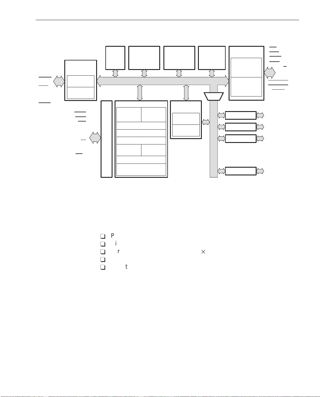
Figure 1–1. TMS320C3x Devices Block Diagram
TMS320C3x Devices
RAM
block 0
1Kx32 (’C30-’C31)
256x32 (’C32)
CPU
Integer and
floating-point
multiplier
8 auxiliary registers
2 index registers
Address
generation 1
12 control registers
2 low-power modes
(’C31-’C32)
IOSTRB
XRDY
XD31-0
XA12-0
MSTRB
Expansion port
(’C30)
memory interface
32-bit
data access
32-bit
program access
RESET
INT3-3
IACK
XF1-0
H1
H3
MCBL/MP
X2/CLKIN
V
DD
E-
VSSSHZ
MU6-0
X1
Program
cache
(64x32)
Integer and
floating-point
multiplier
8 extended-precision registers
Controller
Address
generation 0
1.1.1 TMS320C3x Key Specifications
RAM
block 1
1Kx32 (’C30-’C31)
256 x32 (’C32)
DMA
coprocessor
DMA
channel 0
DMA
channel 1 (’C32)
ROM
4Kx32 (’C30)
boot (’C31-’C32)
Primary port
memory interface
Data access
32-bit (’C30-’C31)
8/16/32-bit (’C32)
Program access
32-bit (’C30-’C31)
16/32-bit (’C32)
Timer 0
Timer 1
Serial port 0
Serial port 1 (’C30)
RDY
HOLD
HOLDA
STRB (’C30-’C31)
R/W
D31-0
A23-0
STRB0_B3-0
STRB1_B3-0
(’C32)
IOSTRB
PRGW (’C32)
TCLK0
TCLK1
CLKX0
DX0
FSX0
CLKR0
DR0
FSR0
CLKX1
DX1
FSX1
CLKR1
DR1
FSR1
(’C32)
(’C32)
The key specifications of the ’C3x devices include the following:
-
Performance up to 60 MFLOPS
-
Highly efficient C language engine
-
Large address space: 16M words 32 bits
-
Fast memory management with on-chip DMA
-
Industry-exclusive 3-V versions available on some devices
1.1.2 TMS320C30
The ’C30 is the first member of the ’C3x generation. It differs from the ’C31 and
’C32 by offering 4K ROM, 2K RAM, a second serial port, and a second external
bus.
1.1.3 TMS320C31 and TMS320LC31
The ’C31 and ’LC31 are the second members of the ’C3x generation. They are
low-cost 32-bit floating-point DSPs which have a boot-loader program, 2K RAM,
single external port, single serial port, and are available in 3.3-V operation
(’LC31).
Introduction
1-3
Page 33

TMS320C3x Devices
1.1.4 TMS320C32
The ’C32 is the newest member of the ’C3x generation. They are enhanced
versions of the ’C3x family and the lowest cost floating-point processors on the
market today. These enhancements include a variable-width memory interface, two-channel DMA coprocessor with configurable priorities, flexible boot
loader, and a relocatable interrupt vector table.
1-4
Page 34
Table 1–1. TMS320C30, TMS320C31, TMS320LC31, and TMS320C32 Comparison
Cycle
Memory (words)
On-Chip Off-Chip Peripherals
Device
Name
Freq
(MHz)
27 75 2K 4K 64 16M 32
Time
(ns)
RAM ROM Cache Parallel Serial
8K 32
DMA
Channels
2 1 2 181 PGA 0° to 85° (commercial)
Timers
Package
Type
Temperature
’C30
(5 V)
’C31
(5 V)
Introduction
’LC31
(3.3 V)
33 60 2K 4K 64 16M 32
8K 32
40 50 2K 4K 64 16M 32
8K 32
50 40 2K 4K 64 16M 32
8K 32
27 75 2K Boot loader 64 16M 32 1 1 2 132 PQFP 0° to 85° (commercial)
33 60 2K Boot loader 64 16M 32 1 1 2 132 PQFP 0° to 85° (commercial)
40 50 2K Boot loader 64 16M 32 1 1 2 132 PQFP 0° to 85° (commercial)
50 40 2K Boot loader 64 16M 32 1 1 2 132 PQFP 0° to 85° (commercial)
60 33 2K Boot loader 64 16M 32 1 1 2 132 PQFP 0° to 85° (commercial)
33 60 2K Boot loader 64 16M 32 1 1 2 132 PQFP 0° to 85° (commercial)
40 50 2K Boot loader 64 16M 32 1 1 2 132 PQFP 0° to 85° (commercial)
21 2181 PGA 0° to 85° (commercial)
21 2181 PGA
208 PQFP
21 2181 PGA
208 PQFP
–55° to 125° (military)
0° to 85° (commercial)
0° to 85° (commercial)
–55° to 125° (military)
–40° to 125° (extended)
–55° to 125° (military)
–40° to 125° (extended)
–55° to 125° (military)
–40° to 125° (extended)
–40° to 125° (extended)
TMS320C3x Devices
1-5
Page 35
1-6
Cycle
TMS320C3x Devices
Table 1–1. TMS320C30, TMS320C31, TMS320LC31, and TMS320C32 Comparison (Continued)
Memory (words)
Device
Name
’C32
(5 V)
On-Chip Off-Chip
Freq
(MHz)
40 50 512 Boot loader 64 16M 32/16/8 1 2 2 144 PQFP 0° to 85° (commercial)
50 40 512 Boot loader 64 16M 32/16/8 1 2 2 144 PQFP 0° to 85° (commercial)
60 33 512 Boot loader 64 16M 32/16/8 1 2 2 144 PQFP 0° to 85° (commercial)
Time
(ns)
RAM
ROM Cache Parallel Serial
Peripherals
DMA
Channels
Timers
Package
Type
Temperature
–40° to 125° (extended)
–40° to 125° (extended)
–55° to 125° (military)
Page 36

1.2 Typical Applications
The TMS320 family’s versatility , realtime performance, and multiple functions
offer flexible design approaches in a variety of applications, which are shown
in Table 1–2.
Table 1–2. Typical Applications of the TMS320 Family
General-Purpose DSP Graphics/Imaging Instrumentation
T ypical Applications
Digital filtering
Convolution
Correlation
Hilbert transforms
Fast Fourier transforms
Adaptive filtering
Windowing
Waveform generation
V oice/Speech Control Military
Voice mail
Speech vocoding
Speech recognition
Speaker verification
Speech enhancement
Speech synthesis
Text-to-speech
Neural networks
T elecommunications Automotive
Echo cancellation
ADPCM transcoders
Digital PBXs
Line repeaters
Channel multiplexing
Modems
Adaptive equalizers
DTMF encoding/decoding
Data encryption
3-D transformations rendering
Robot vision
Image transmission/compression
Pattern recognition
Image enhancement
Homomorphic processing
Workstations
Animation/digital map
Bar-code scanners
Disk control
Servo control
Robot control
Laser printer control
Engine control
Motor control
Kalman filtering
FAX
Cellular telephones
Speaker phones
Digital speech
Interpolation (DSI)
X.25 packet switching
Video conferencing
Spread spectrum
Communications
Spectrum analysis
Function generation
Pattern matching
Seismic processing
Transient analysis
Digital filtering
Phase-locked loops
Secure communications
Radar processing
Sonar processing
Image processing
Navigation
Missile guidance
Radio frequency modems
Sensor fusion
Engine control
Vibration analysis
Antiskid brakes
Anticollision
Adaptive ride control
Global positioning
Navigation
Voice commands
Digital radio
Cellular telephones
Consumer Industrial Medical
Radar detectors
Power tools
Digital audio/TV
Music synthesizer
Toys and games
Solid-state answering
Machines
Robotics
Numeric control
Security access
Power line monitors
Visual inspection
Lathe control
CAM
Hearing aids
Patient monitoring
Ultrasound equipment
Diagnostic tools
Prosthetics
Fetal monitors
MR imaging
Introduction
Introduction
1-7
Page 37

Chapter 2
Architectural Overview
This chapter provides an architectural overview of the ’C3x processor. It includes
a discussion of the CPU, memory interface, boot loader, peripherals, and direct
memory access (DMA) of the ’C3x processor.
Topic Page
2.1 Overview 2-2. . . . . . . . . . . . . . . . . . . . . . . . . . . . . . . . . . . . . . . . . . . . . . . . . . . . .
2.2 Central Processing Unit (CPU) 2-6. . . . . . . . . . . . . . . . . . . . . . . . . . . . . . . . .
2.3 CPU Primary Register File 2-9. . . . . . . . . . . . . . . . . . . . . . . . . . . . . . . . . . . . .
2.4 Other Registers 2-12. . . . . . . . . . . . . . . . . . . . . . . . . . . . . . . . . . . . . . . . . . . . . .
2.5 Memory Organization 2-13. . . . . . . . . . . . . . . . . . . . . . . . . . . . . . . . . . . . . . . .
2.6 Internal Bus Operation 2-18. . . . . . . . . . . . . . . . . . . . . . . . . . . . . . . . . . . . . . .
2.7 External Memory Interface 2-19. . . . . . . . . . . . . . . . . . . . . . . . . . . . . . . . . . . .
2.8 Interrupts 2-21. . . . . . . . . . . . . . . . . . . . . . . . . . . . . . . . . . . . . . . . . . . . . . . . . . .
2.9 Peripherals 2-22. . . . . . . . . . . . . . . . . . . . . . . . . . . . . . . . . . . . . . . . . . . . . . . . . .
2.10 Direct Memory Access (DMA) 2-24. . . . . . . . . . . . . . . . . . . . . . . . . . . . . . . . .
2.11 TMS320C30, TMS320C31, and TMS320C32 Differences 2-26. . . . . . . . . .
2-1
Page 38

Overview
2.1 Overview
The ’C3x architecture responds to system demands that are based on sophisticated arithmetic algorithms that emphasize both hardware and software solutions. High performance is achieved through the precision and wide dynamic
range of the floating-point units, large on-chip memory , a high degree of parallelism, and the DMA controller.
Figure 2–1 through Figure 2–3 show functional block diagrams of the ’C30,
’C31, and ’C32 architectures, respectively.
2-2
Page 39
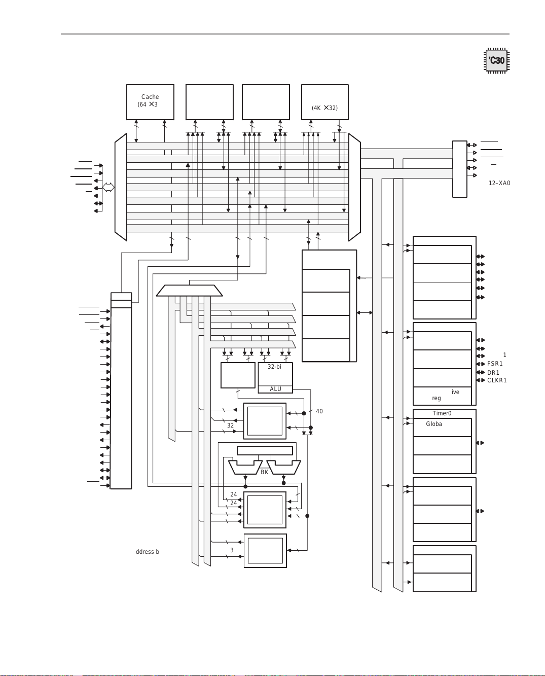
Figure 2–1. TMS320C30 Block Diagram
0
0
Overview
Cache
(64
32 24 24 24 2432 32 32
PDATA bus
RDY
HOLD
HOLDA
STRB
R/W
D31–D0
A23–A0
RESET
INT3–0
IACK
MC/MP
XF(1,0)
VDD(3-0)
IODVDD(1,0)
ADVDD(1,0)
PDV
DD
DDVDD(1,0)
MDV
DD
VSS(3-0)
DVSS(3–0)
CVSS(1,0)
IV
SS
V
BBP
SUBS
X1
X2/CLKIN
H1
H3
EMU6-0
RSV10–0
SHZ
Legend:
PDATA bus – program data bus
PADDR bus – program address bus
DDATA bus – data data bus
DADDR1 bus – data address 1 bus
DADDR2 bus – data address 2 bus
PADDR bus
DDATA bus
DADDR1 bus
Multiplexer
DADDR2 bus
DMADATA bus
DMAADDR bus
IR
PC
Controller
RAM
24
Multiplexer
CPU1
block 0
× 32)
(1K
32 32 40 40
Multiplier
REGISTER2
REGISTER 1
40
40
40
32
× 32)
32 32 24 24 32 24
RAM
block 1
× 32)
(1K
CPU1
CPU2
REG1
REG2
32-bit
barrel
shifter
ALU
Extended-
precision
registers
(R7–R0)
DISP0, IR0, IR1
ARAU0 ARAU1
BK
24
Auxiliary
24
registers
32
(AR0–AR7)
32
32
Other
registers
32
(12)
40
40
24
24
32
32
ROM
block
(4K
× 32)
DMA controller
Global-control
register
Source-address
register
Destination-
address
register
Transfer-
counter
register
40
Multiplexer
Peripheral Data Bus
Peripheral Address Bus
Serial port 0
Port-control
register
R/X timer
register
Data-transmit
register
Data-receive
register
Serial port 1
Port-control
register
R/Xtimer
register
Data-transmit
register
Data-receive
register
Timer0
Global-control
register
Timer-period
register
Timer-counter
register
Timer1
Global-control
register
Timer-period
register
Timer-counter
register
Port control
Primary
Expansion
XRDY
MSTRB
IOSTRB
XR/W
XD31–XD
XA12–XA
FSX0
DX0
CLKX0
FSR0
DR0
CLKR0
FSX1
DX1
CLKX1
FSR1
DR1
CLKR1
TCLK0
TCLK1
Architectural Overview
2-3
Page 40
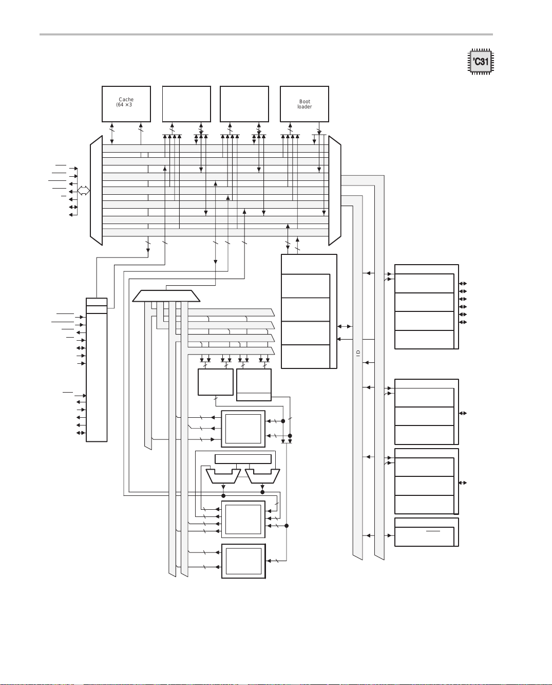
Overview
Figure 2–2. TMS320C31 Block Diagram
Cache
(64 × 32)
32 24 24
PDATA bus
Multiplexer
IR
PC
Controller
PADDR bus
DDATA bus
DADDR1 bus
DADDR2 bus
DMADATA bus
DMAADDR bus
RDY
HOLD
HOLDA
STRB
R/W
D31–D0
A23– A0
RESET
INT(3– 0)
IACK
MCBL/ MP
XF(1,0)
V
(19– 0)
DD
VSS(24– 0)
SHZ
X2/ CLKIN
EMU(3– 0)
X1
H1
H3
Legend:
PDATA bus – program data bus
PADDR bus – program address bus
DDATA bus – data data bus
DADDR1 bus – data address 1 bus
DADDR2 bus – data address 2 bus
32
Multiplexer
CPU1
RAM
block 0
(1K × 32)
24
32 32 40 40
REG1
REG2
RAM
block 1
(1K × 32)
24 2432 32 32
Multiplier
40
40
40
32
24
24
32
32
32
32
24
32
CPU1
CPU2
REG1
REG2
Extended-
precision
registers
(R7–R0)
DISP0, IR0, IR1
ARAU0
Auxiliary
registers
(AR0– AR7)
registers
BK
Other
(12)
24
32-bit
barrel
shifter
ALU
32
40
40
ARAU1
24
24
32
32
Boot
loader
24
DMA controller
Global-control
register
Source-address
register
Destination-
address
register
Transfer-
counter
register
40
MUX
Multiplexer
Peripheral Data Bus
Peripheral Address Bus
Serial port 0
Serial-port control
register
Receive/transmit
timer register
Data-transmit
register
Data-receive
register
Timer0
Global-control
register
Timer-period
register
Timer-counter
register
Timer1
Global-control
register
Timer-period
register
Timer-counter
register
Port Control
Primary STRB
control register
FSX0
DX0
CLKX0
FSR0
DR0
CLKR0
TCLK0
TCLK1
-
2-4
Page 41
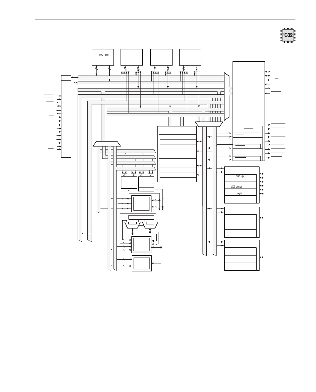
Figure 2–3. TMS320C32 Block Diagram
Overview
32
IR
PC
24
RESET
INT(3-0)
IACK
XF(1,0)
H1
H3
MCBL/ MP
CLKIN
CV
SS
DVSS(6-0)
IV
SS
DV
DD
V
DDL
V
SSL
V
EMU0–3
(6-0)
(3-9)
(11-3)
(7-0)
(5-0)
SUBS
SHZ
Controller
Legend:
PDATA bus – program data bus
PADDR bus – program address bus
DDATA bus – data data bus
DADDR1 bus – data address 1 bus
DADDR2 bus – data address 2 bus
PDATA bus
PADDR bus
DDATA bus
DADDR1 bus
Program
cache
(64 × 32)
32 24
Multiplexer
CPU1
24
DADDR2 bus
DMADATA bus
DMAADDR bus
32 32 40
REG1
REG2
Multiplier
40
40
32
RAM
block 0
(256 × 32)
CPU1
CPU2
REG1
REG2
40
32-bit
barrel
shifter
40
Extended-
precision
registers
(R0–R7)
DISP0, IR0, IR1
ARAU0 ARAU1
BK
24
Auxiliary
24
registers
32
(AR0–AR7)
32
32
Other
registers
32
(12)
RAM
block 1
(256 × 32)
24 2432 32 32
DMA controller
DMA channel 0
Global-controlregister
Source-addressregister
Destination-addressregister
Transfer-counter rregister
DMA channel 1
Global-controlregister
Source-addressregister
Destination register
Transfer-counter
ALU
40
40
40
24
24
32
32
Boot
ROM
Multiplexer
Peripheral data bus
Peripheral address bus
External
memory
interface
Multiplexer
STRB0
STRB0 control reg.
STRB1
control reg.
STRB1
IOSTRB
IOSTRB
control reg.
Serial port
Serial-port
controlregister
Receive/transmit
(R/X) timer register
Data-transmit
register
Data-receive
register
Timer0
Global-control
register
Timer-period
register
Timer-counter
register
Timer1
Global-control
register
Timer-period
register
Timer-counter
register
A23– A0
D31– D0
R/W
RDY
HOLD
HOLDA
PRGW
STRB0_B3/A
STRB0_B2/A
STRB0_B1
STRB0_B0
STRB1_B3/A
STRB1_B2/A
STRB1_B1
STRB1_B0
IOSTRB
FSX0
DX0
CLKX0
FSR0
DR0
CLKR0
TCLK0
TCLK1
–1
–2
–1
–2
Architectural Overview
2-5
Page 42

Central Processing Unit (CPU)
2.2 Central Processing Unit (CPU)
The ’C3x devices (’C30, ’C31, and ’C32) have a register-based CPU architecture. The CPU consists of the following components:
-
Floating-point/integer multiplier
-
Arithmetic logic unit (ALU)
-
32-bit barrel shifter
-
Internal buses (CPU1/CPU2 and REG1/REG2)
-
Auxiliary register arithmetic units (ARAUs)
-
CPU register file
Figure 2–4 shows a diagram of the various CPU components.
2-6
Page 43

Figure 2–4. Central Processing Unit (CPU)
DADDR1 bus
DADDR2 bus
DDATA bus
Multiplexer
Central Processing Unit (CPU)
CPU1 bus
CPU2 bus
REG1 bus
REG2 bus
DADDR1 bus
DADDR2 bus
†
Disp = an 8-bit integer displacement carried in a program-control instruction
CPU1 bus
REG1 bus
REG2 bus
40
40
32
32 32 40 40
Multiplier
40
Extended-
precision
registers
(R0–R7)
Disp†, IR0, IR1
ARAU0 ARAU1
24
24
32
32
32
32
BK
Auxiliary
registers
(AR0–AR7)
Other
registers
(12)
32-bit barrel
shifter
ALU
40
40
40
24
24
32
32
Architectural Overview
2-7
Page 44

Central Processing Unit (CPU)
2.2.1 Floating-Point/Integer Multiplier
The multiplier performs single-cycle multiplications on 24-bit integer and 32-bit
floating-point values. The ’C3x implementation of floating-point arithmetic allows
for floating-point or fixed-point operations at speeds up to 33-ns per instruction
cycle. T o gain even higher throughput, you can use parallel instructions to perform
a multiply and an ALU operation in a single cycle.
When the multiplier performs floating-point multiplication, the inputs are 32-bit
floating-point numbers, and the result is a 40-bit floating-point number. When
the multiplier performs integer multiplication, the input data is 24 bits and yields
a 32-bit result. See Chapter 5,
detailed information.
Data Formats and Floating-Point Operation,
2.2.2 Arithmetic Logic Unit (ALU) and Internal Buses
The ALU performs single-cycle operations on 32-bit integer, 32-bit logical,
and 40-bit floating-point data, including single-cycle integer and floatingpoint conversions. Results of the ALU are always maintained in 32-bit integer
or 40-bit floating-point formats. The barrel shifter is used to shift up to 32 bits
left or right in a single cycle. See Chapter 5,
Operation,
for detailed information.
for
Data Formats and Floating-Point
Four internal buses, CPU1, CPU2, REG1, and REG2 carry two operands from
memory and two operands from the register file, allowing parallel multiplies
and adds/subtracts on four integer or floating-point operands in a single cycle.
2.2.3 Auxiliary Register Arithmetic Units (ARAUs)
Two auxiliary register arithmetic units (ARAU0 and ARAU1) can generate two
addresses in a single cycle. The ARAUs operate in parallel with the multiplier
and ALU. They support addressing with displacements, index registers (IR0 and
IR1), and circular and bit-reversed addressing. See Chapter 6,
2-8
Modes,
for more information.
Addressing
Page 45

2.3 CPU Primary Register File
The ’C3x provides 28 registers in a multiport register file that is tightly coupled
to the CPU. Table 2–1 lists the register names and functions.
All of the primary registers can be operated upon by the multiplier and ALU and
can be used as general-purpose registers. The registers also have some special
functions. For example, the eight extended-precision registers are especially
suited for maintaining extended-precision floating-point results. The eight auxiliary
registers support a variety of indirect addressing modes and can be used as
general-purpose 32-bit integer and logical registers. The remaining registers
provide such system functions as addressing, stack management, processor
status, interrupts, and block repeat. See Chapter 3,
information.
Table 2–1. Primary CPU Registers
Register
Name
R0 Extended-precision register 0 3.1.1 3-3
R1 Extended-precision register 1 3.1.1 3-3
CPU Primary Register File
CPU Registers,
Assigned Function Section Page
for more
R2
R3
R4
R5
R6
R7
AR0
AR1
AR2
AR3
AR4
AR5
AR6
AR7
DP
Extended-precision register 2 3.1.1 3-3
Extended-precision register 3 3.1.1 3-3
Extended-precision register 4 3.1.1 3-3
Extended-precision register 5 3.1.1 3-3
Extended-precision register 6 3.1.1 3-3
Extended-precision register 7 3.1.1 3-3
Auxiliary register 0 3.1.2 3-4
Auxiliary register 1 3.1.2 3-4
Auxiliary register 2 3.1.2 3-4
Auxiliary register 3 3.1.2 3-4
Auxiliary register 4 3.1.2 3-4
Auxiliary register 5 3.1.2 3-4
Auxiliary register 6 3.1.2 3-4
Auxiliary register 7 3.1.2 3-4
Data-page pointer 3.1.3 3-4
IR0 Index register 0 3.1.4 3-4
Architectural Overview
2-9
Page 46

CPU Primary Register File
Table 2–1. Primary CPU Registers (Continued)
Register
Name
IR1 Index register 1 3.1.4 3-4
BK Block-size register 3.1.5 3-4
PageSectionAssigned Function
SP
ST
IE
IF
IOF
RS
RE
RC Repeat counter 3.1.11 3-17
System-stack pointer 3.1.6 3-4
Status register 3.1.7 3-5
CPU/DMA interrupt-enable regis-
ter
CPU interrupt flag 3.1.9 3-11
I/O flag 3.1.10 3-16
Repeat start-address 3.1.11 3-17
Repeat end-address 3.1.1 1 3-17
3.1.8 3-9
The extended-precision registers (R7–R0) can store and support operations
on 32-bit integers and 40-bit floating-point numbers. Any instruction that assumes
the operands are floating-point numbers uses bits 39–0. If the operands are
either signed or unsigned integers, only bits 31–0 are used; bits 39–32 remain
unchanged. This is true for all shift operations. See Chapter 5,
Floating-Point Operation,
for extended-precision register formats for floating-
Data Formats and
point and integer numbers.
The 32-bit auxiliary registers (AR7–AR0) are accessed by the CPU and
modified by the two ARAUs. The primary function of the auxiliary registers is
the generation of 24-bit addresses. They also can be used as loop counters
or as 32-bit general-purpose registers that are modified by the multiplier and
ALU. See Chapter 6,
Addressing Modes
, for detai led inform ation and ex amples
of the use of auxiliary registers in addressing.
2-10
The data-page pointer (DP) is a 32-bit register . The eight least significant bits
(LSBs) of the data-page pointer are used by the direct addressing mode as a
pointer to the page of data being addressed. Data pages are 64K words long,
with a total of 256 pages.
The 32-bit index registers (IR0, IR1) contain the value used by the ARAU to
compute an indexed address. See Chapter 6,
Addressing Modes
, for examples
of the use of index registers in addressing.
Page 47

CPU Primary Register File
The ARAU uses the 32-bit block size register (BK) in circular addressing to
specify the data block size.
The system-stack pointer (SP) is a 32-bit register that contains the address
of the top of the system stack. The SP always points to the last element pushed
onto the stack. A
performs a preincrement; a
pop
performs a postdecre-
push
ment of the system-stack pointer. The SP is manipulated by interrupts, traps,
calls, returns, and the PUSH and POP instructions. See Section 6.10,
and User Stack Management
, on page 6-29, for more information.
System
The status register (ST) contains global information relating to the state of the
CPU. Operations usually set the condition flags of the status register according
to whether the result is 0, negative, etc. These include register load and store
operations as well as arithmetic and logical functions. When the status register
is loaded, however, a bit-for-bit replacement is performed with the contents of
the source operand, regardless of the state of any bits in the source operand.
Following a load, the contents of the status register are identical to the contents
of the source operand. This allows the status register to be easily saved and
restored. See T able 3–2 on page 3-6 for a list and definitions of the status register bits.
The CPU/DMA interrupt-enable register (IE) is a 32-bit register. The CPU
interrupt-enable bits are in locations 10–0. The DMA interrupt-enable bits are
in locations 26–16. A 1 in a CPU/DMA interrupt-enable register bit enables the
corresponding interrupt. A 0 disables the corresponding interrupt. See Section 3.1.8 on page 3-9 for more information.
The CPU interrupt flag register (IF) is also a 32-bit register. A 1 in a CPU
interrupt flag register bit indicates that the corresponding interrupt is set. A
0 indicates that the corresponding interrupt is not set. See Section 3.1.9 on
page 3-11 for more information.
The I/O flag register (IOF) controls the function of the dedicated external pins,
XF0 and XF1. These pins may be configured for input or output and may also
be read from and written to. See Section 3.1.10 on page 3-16 for more information.
The repeat-counter (RC) is a 32-bit register that specifies the number of times
to repeat a block of code when performing a block repeat. When the processor
is operating in the repeat mode, the 32-bit
repeat start-address register (RS)
contains the starting address of the block of program memory to repeat, and
the 32-bit
repeat end-address register (RE)
contains the ending address of the
block to repeat.
Architectural Overview
2-11
Page 48

Other Registers
2.4 Other Registers
The program-counter (PC) is a 32-bit register containing the address of the
next instruction to fetch. Although the PC is not part of the CPU register file,
it is a register that can be modified by instructions that modify the program flow.
The instruction register (IR) is a 32-bit register that holds the instruction opcode
during the decode phase of the instruction. This register is used by the instruction
decode control circuitry and is not accessible to the CPU.
2-12
Page 49

2.5 Memory Organization
The total memory space of the ’C3x is 16M (million) 32-bit words. Program,
data, and I/O space are contained within this 16M-word address space, allowing
the storage of tables, coefficients, program code, or data in either RAM or
ROM. In this way , memory usage is maximized and memory space allocated
as desired.
2.5.1 RAM, ROM, and Cache
Figure 2–5 shows how the memory is organized on the ’C30. RAM blocks 0
and 1 are each 1K 32 bits. The ROM block, available only on the ’C30, is
4K 32 bits. Each RAM and ROM block is capable of supporting two CPU
accesses in a single cycle.
Figure 2–6 shows how the memory is organized on the ’C31. RAM blocks 0
and 1 are each 1K 32 bits and support two accesses in a single cycle. A boot
loader allows the loading of program and data at reset from 8-, 16-, 32-bit-wide
memories or serial port.
Figure 2–7 shows how the memory is organized on the ’C32. RAM blocks 0
and 1 are each 256 32 bits and support two accesses in a single cycle. A
boot loader allows the loading of program and data at reset from 1-, 2-, 4-, 8-,
16-, and 32-bit-wide memories or serial port. The ’C32 enhanced external
memory interface provides the flexibility to address 8-, 16-, or 32-bit data independently of the external memory width. The external memory width can be 8-, 16-,
or 32-bits wide.
Memory Organization
The ’C3x’s separate program, data, and DMA buses allow for parallel program
fetches, data reads and writes, and DMA operations. For example, the CPU can
access two data values in one RAM block and perform an external program
fetch in parallel with the DMA controller loading another RAM block, all within
a single cycle.
Architectural Overview
2-13
Page 50
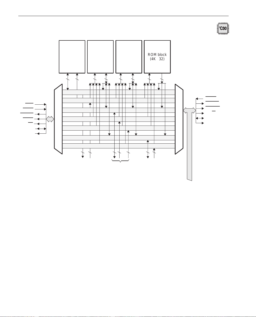
Memory Organization
Figure 2–5. Memory Organization of the TMS320C30
RDY
HOLD
HOLDA
STRB
R/W
D31–D0
A23–A0
Cache
(64 32)
32 24 24 32 24 24 32
PDATA bus
PADDR bus
DDATA bus
DADDR1 bus
Multiplexer
DADDR2 bus
DMADATA bus
DMAADDR bus
32 24 32 24 24 32 24
Program counter/
instruction register
RAM
block 0
(1K 32)
block 1
(1K 32)
CPU
RAM
32
controller
ROM block
(4K 32)
XRDY
MSTRB
IOSTRB
XR/W
XD31–XD0
XA12–XA0
Multiplexer
Peripheral bus
DMA
2-14
Page 51
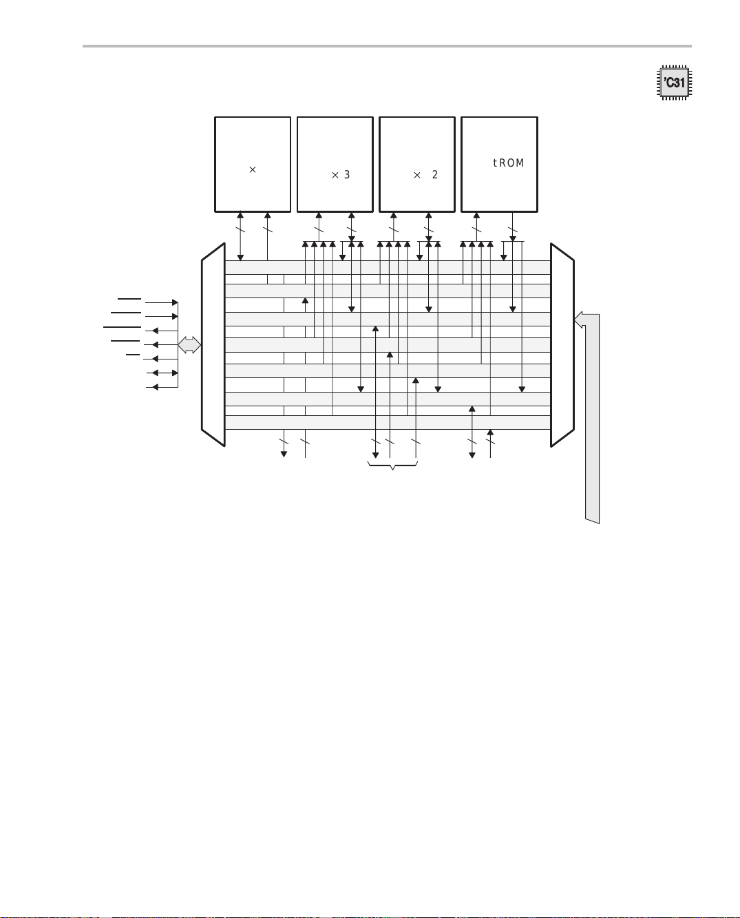
Figure 2–6. Memory Organization of the TMS320C31
Memory Organization
RDY
HOLD
HOLDA
STRB
R/W
D31–D0
A23–A0
Cache
(64 32)
32 24 24 32 24 24 32
PDATA bus
PADDR bus
DDATA bus
DADDR1 bus
Multiplexer
DADDR2 bus
DMADATA bus
DMAADDR bus
32 24 32 24 24 32 24
Program counter/
instruction register
RAM
block 0
(1K 32)
RAM
block 1
(1K 32)
CPU
32
controller
Boot ROM
Multiplexer
Peripheral bus
DMA
Architectural Overview
2-15
Page 52
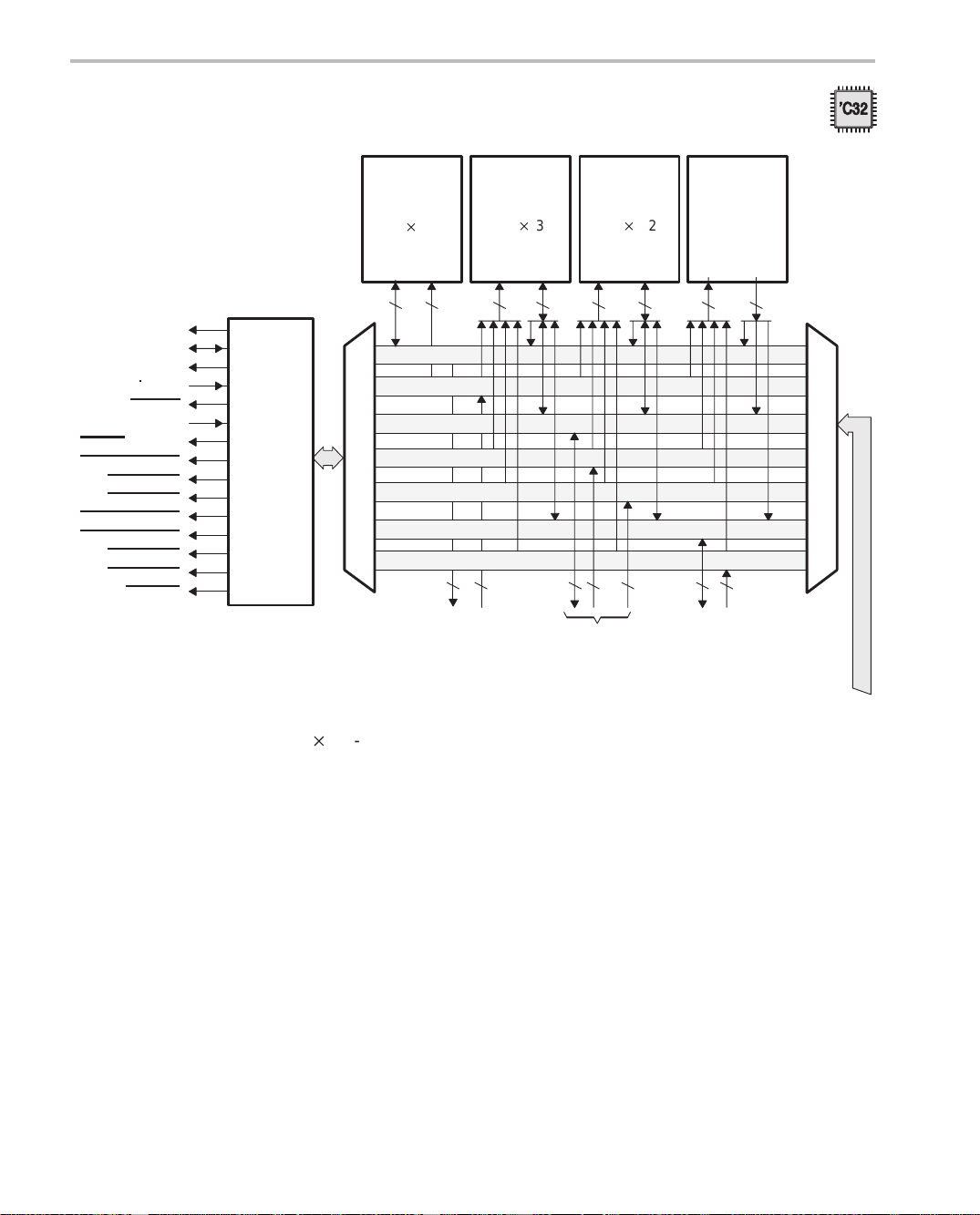
Memory Organization
Figure 2–7. Memory Organization of the TMS320C32
A23–A0
D31–D0
R/W
HOLD
HOLDA
PRGW
STRB0_B3/A-1
STRB0_B2/A-2
STRB0_B1
STRB0_B0
STRB1_B3/A-1
STRB1_B2/A-2
STRB1_B1
STRB1_B0
IOSTRB
Enhanced
external
memory
interface
RAM
Cache
(64 32)
32 24 24 32 24 24 32
PDATA bus
PADDR bus
DDATA bus
DADDR1 bus
Multiplexer
DADDR2 bus
DMADATA bus
DMAADDR bus
32 24 32 24 24 32 24
Program counter/
instruction register
block 0
(256 32)
RAM
block 1
(256 32)
CPU
32
controller
Boot ROM
Multiplexer
Peripheral bus
DMA
2-16
A 64 32-bit instruction cache is provided to store often-repeated sections
of code, which greatly reduces the number of off-chip accesses. This allows
for code to be stored off chip in slower, lower-cost memories. The external
buses are also freed for use by the DMA, external memory fetches, or other
devices in the system.
See Chapter 4,
Memory and the Instruction Cache
, for more information.
Page 53

2.5.2 Memory Addressing Modes
The ’C3x supports a base set of general-purpose instructions as well as arithmeticintensive instructions that are particularly suited for digital signal processing and
other numeric-intensive applications. See Chapter 6,
information.
Four groups of addressing modes are provided on the ’C3x. Each group uses
two or more of several different addressing types. The following list shows the
addressing modes with their addressing types.
-
General instruction addressing modes:
J
Register. The operand is a CPU register.
J
Short immediate. The operand is a 16-bit (short) or 24-bit (long) immediate value.
J
Direct. The operand is the contents of a 24-bit address formed by
concatenating the 8 bits of data-page pointer and a 16-bit operand.
J
Indirect. An auxiliary register indicates the address of the operand.
Memory Organization
Addressing Modes
, fo r mo re
-
3-operand instruction addressing modes:
J
Register. Same as for general addressing mode.
J
Indirect. Same as for general addressing mode.
-
Parallel instruction addressing modes:
J
Register. The operand is an extended-precision register.
J
Indirect. Same as for general addressing mode.
-
Branch instruction addressing modes:
J
Register. Same as for general addressing mode.
J
PC-relative. A signed 16-bit displacement or a 24-bit displacement is
added to the PC.
Architectural Overview
2-17
Page 54

Internal Bus Operation
2.6 Internal Bus Operation
Much of the ’C3x’s high performance is due to internal busing and parallelism.
Separate buses allow for parallel program fetches, data accesses, and DMA
accesses:
-
Program buses: PADDR and PDATA
-
Data buses: DADDR1, DADDR2, and DDA TA
-
DMA buses: DMAADDR and DMADA TA
These buses connect all of the physical spaces (on-chip memory, off-chip
memory, and on-chip peripherals) supported by the ’C3x. Figure 2–5,
Figure 2–6, and Figure 2–7 show these internal buses and their connections
to on-chip and off-chip memory blocks.
The program counter (PC) is connected to the 24-bit program address bus
(P ADDR). The instruction register (IR) is connected to the 32-bit program data
bus (PDA T A). These buses can fetch a single instruction word every machine
cycle.
The 24-bit data address buses (DADDR1 and DADDR2) and the 32-bit data
data bus (DDATA) support two data-memory accesses every machine cycle.
The DDATA bus carries data to the CPU over the CPU1 and CPU2 buses. The
CPU1 and CPU2 buses can carry two data-memory operands to the multiplier,
ALU, and register file every machine cycle. Also internal to the CPU are register
buses REG1 and REG2, which can carry two data values from the register file
to the multiplier and ALU every machine cycle. Figure 2–4 shows the buses
internal to the CPU section of the processor.
2-18
The DMA controller is supported with a 24-bit address bus (DMAADDR) and
a 32-bit data bus (DMADA TA). These buses allow the DMA to perform memory
accesses in parallel with the memory accesses occurring from the data and
program buses.
Page 55

2.7 External Memory Interface
The ’C30 provides two external interfaces: the primary bus and the expansion
bus. The ’C31 provides one external interface: the primary bus. The ’C32 provides one enhanced external interface with three independent multi-function
strobes. These buses consist of a 32-bit data bus and a set of control signals. The
primary and enhanced memory buses have a 24-bit address bus, whereas the
expansion bus has a 13-bit address bus. These buses address external program/
data memory or I/O space. The buses also have external RDY
state generation. You can insert additional wait states under software control.
Chapter 9,
The ’C3x family was designed for 32-bit instructions and 32-bit data operations.
This architecture has many advantages, including a high degree of parallelism
and provisions for a C compiler. However, the ’C30 and ’C31 require a 32-bit-wide
external memory even when the data requires only 8- or 16-bit-wide memories.
The ’C32 enhanced external memory interface overcomes this limitation by providing the flexibility to address 8-, 16-, or 32-bit data independently of the external memory width. In this way, the chip count and the size of external memory
is reduced. The number of memory chips can be further reduced by the ’C32’s
ability to allow code execution from 16- or 32-bit-wide memories. The ’C32
memory interface also reduces the total amount of RAM by allowing the physical
data memory to be 8, 16, or 32 bits wide. Internally, the ’C32 has a 32-bit architecture. So you can treat the ’C32 as a 32-bit device regardless of the physical
external memory width. The external memory interface handles the conversion
between external memory width and ’C32 internal 32-bit architecture.
External Memory Interface
External Memory Interface
signals for wait-
, covers external bus operation.
2.7.1 TMS320C32 16- and 32-Bit Program Memory
The ’C32 executes code from either 16- or 32-bit-wide memories. When
connected to 32-bit memories, ‘C32 program execution is identical to that
of the ’C31. When connected to 16-bit zero wait-state memory, the ’C32
takes two instruction cycles to fetch a single 32-bit instruction. During the
first cycle, the ’C32 fetches the lower 16 bits. During the second cycle, the
’C32 fetches the upper 16 bits and concatenates them with the previously
fetched lower 16 bits. This process occurs entirely within the memory interface and is transparent to you. An external pin, PRGW
program memory width.
, dictates the external
Architectural Overview
2-19
Page 56
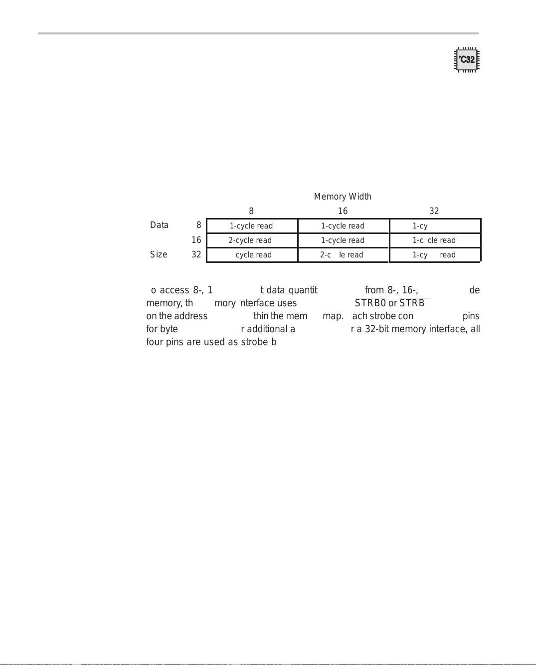
External Memory Interface
2.7.2 TMS320C32 8-, 16-, and 32-Bit Data Memory
The ’C32 external memory interface can load and store 8-, 16-, or 32-bit quantities into external memory and convert them into an internally-equivalent 32-bit
representation. The external memory interface accomplishes this without
changing the CPU instruction set. Figure 2–8 shows the supported external
memory widths, data types and sizes for zero wait-state memory and the associated cycle count.
Figure 2–8. TMS320C32-Supported Data Types and Sizes and External Memory Widths
Memory Width
8
Data
Type
Size
16
32
8
1-cycle read
2-cycle read
4-cycle read
To access 8-, 16-, or 32-bit data quantities (types) from 8-, 16-, or 32-bit-wide
memory , the memory interface uses either strobe STRB0 or STRB1, depending
on the address location within the memory map. Each strobe consists of four pins
for byte enables and/or additional addresses. For a 32-bit memory interface, all
four pins are used as strobe byte-enable pins. These strobe byte-enable pins
select one or more bytes of the external memory . For a 16-bit memory interface,
the ’C32 uses one of these pins as an additional address pin, while using two
pins as strobe byte-enable pins. For an 8-bit memory interface, the ’C32 uses
two of these pins as additional address pins while using one pin as strobe pin.
The ’C32 manipulates the behavior of these pins according to the contents of
the bus control registers (one control register per strobe). By setting a few bit
fields in this register, you indicate the data-type size and external memory width.
16
1-cycle read
1-cycle read
2-cycle read
32
1-cycle read
1-cycle read
1-cycle read
2-20
Page 57

2.8 Interrupts
Interrupts
The ’C3x supports four external interrupts (INT3–INT0), a number of internal
interrupts, and a nonmaskable external RESET
interrupt either the DMA or the CPU. When the CPU responds to the interrupt,
the IACK pin can be used to signal an external interrupt acknowledge. Section
7.5,
Reset Operation
The ’C30 and ’C31 external interrupts are level-triggered. To reduce external
logic and simplify the interface, the ’C32 external interrupts are edge- and levelor level-only triggered. The triggering is user-selectable through a bit in the
status register . See Section 3.1.7,
, on page 7-21 covers RESET and interrupt processing.
Status Register (ST)
signal. These can be used to
, for more information.
Two external I/O flags, XF0
under software control. These pins are also used by the interlocked operations
of the ’C3x. The interlocked-operations instruction group supports multiprocessor communication. See Section 7.4,
examples.
and XF1, can be configured as input or output pins
Interlocked Operations
, on page 7-13 for
Architectural Overview
2-21
Page 58

Peripherals
2.9 Peripherals
All ’C3x peripherals are controlled through memory-mapped registers on a dedicated peripheral bus. This peripheral bus is composed of a 32-bit data bus and
a 24-bit address bus. This peripheral bus permits straightforward communication to the peripherals. The ’C3x peripherals include two timers and two serial
ports (only one serial port and one DMA coprocessor are available on the ’C31
and one serial port and two DMA coprocessor channels on the ’C32).
Figure 2–9 shows these peripherals with their associated buses and signals.
See Chapter 12,
Figure 2–9. Peripheral Modules
Memory
space
Peripherals
, for more information.
Serial port 0
Port-control register
R/X timer register
Data-transmit register
Data-receive register
FSX0
DX0
CLKX0
FSR0
DR0
CLKR0
Peripheral data bus
Peripheral address bus
Available on ’C30
Serial port 1
Port-control register
R/X timer register
Data-transmit register
Data-receive register
Timer0
Global-control register
Timer-period register
Timer-counter register
Timer1
Global-control register
Timer-period register
Timer-counter register
FSX1
DX1
CLKX1
FSR1
DR1
CLKR1
TCLK0
TCLK1
2-22
Page 59

2.9.1 Timers
2.9.2 Serial Ports
Peripherals
The two timer modules are general-purpose 32-bit timer/event counters with
two signaling modes and internal or external clocking. They can signal internally
to the ’C3x or externally to the outside world at specified intervals or they can
count external events. Each timer has an I/O pin that can be used as an input
clock to the timer , as an output signal driven by the timer, or as a general-purpose
I/O pin. See Chapter 12,
Peripherals
, for more information about timers.
The bidirectional serial ports (two on ’C30, one each on the ’C31 and ’C32) are
totally independent. They are identical to a complementary set of control registers
that control each port. Each serial port can be configured to transfer 8, 16, 24,
or 32 bits of data per word. The clock for each serial port can originate either
internally or externally. An internally generated divide-down clock is provided.
The pins are configurable as general-purpose I/O pins. The serial ports can also
be configured as timers. A special handshake mode allows ’C3x devices to
communicate over their serial ports with guaranteed synchronization.
Architectural Overview
2-23
Page 60

Direct Memory Access (DMA)
2.10 Direct Memory Access (DMA)
The on-chip DMA controller can read from or write to any location in the
memory map without interfering with the CPU operation. The ’C3x can interface to slow, external memories and peripherals without reducing throughput
to the CPU. The DMA controller contains its own address generators, source
and destination registers, and transfer counter. Dedicated DMA address and
data buses minimize conflicts between the CPU and the DMA controller. A
DMA operation consists of a block or single-word transfer to or from memory .
See Section 12.3,
Figure 2–10 shows the DMA controller and its associated buses.
The ’C30 and ’C31 DMA coprocessors have one channel, while the ’C32 DMA
coprocessor has two channels. Each channel of the ’C32 DMA coprocessor is
equivalent to the ’C30/31 DMA with the addition of user-configurable priorities.
Because the DMA and CPU have distinct buses on the ’C3x devices, they can
operate independently of each other. However, when the CPU and DMA access
the same on-chip or external resources, the bandwidth can be exceeded and
priorities must be established. The ’C30 and ’C31 assign highest priority to the
CPU. The ’C32 DMA coprocessor provides more flexibility by allowing you to
choose one of the following priorities:
DMA Controller
, on page 12-48 for more information.
-
CPU: For all resource conflicts, the CPU has priority over the DMA.
-
DMA: For all resource conflicts, the DMA has priority over the CPU.
-
Rotating: When the CPU and DMA have a resource conflict during consecutive instruction cycles, the CPU is granted priority. On the following
cycle, the DMA is granted priority . Alternate access continues as long as
the CPU and DMA requests conflict in consecutive instruction cycles.
The DMA/CPU priority is configured by the DMA PRI bit fields of the corresponding
DMA global-control register. See Section 12.3,
DMA Controller
, on page 12-48 for
a complete description.
2-24
Page 61

Figure 2–10. DMA Controller
DMAADDR bus
DMADATA bus
DMA controller
Global-control register
Direct Memory Access (DMA)
Peripheral data bus
Source-address register
Destination-address register
Transfer-counter register
Peripheral address bus
Architectural Overview
2-25
Page 62

TMS320C30, TMS320C31, and TMS320C32 Differences
2.11 TMS320C30, TMS320C31, and TMS320C32 Differences
Table 2–2 shows the major differences between the ’C32, ’C31, and the ’C30
devices.
2-26
Page 63

TMS320C30, TMS320C31, and TMS320C32 Differences
Table 2–2. Feature Set Comparison
Feature ’C30 ’C31 ’C32
External bus Two buses:
-
Primary bus:
32-bit data
24-bit address
active for
STRB
0h–7FFFFFh and
80A000h–FFFFFFh
-
Expansion bus:
32-bit data
13-bit address
MSTRB
active for
800000h–801FFFh
IOSTRB
active for
804000h–805FFFh
ROM 4k No No
One bus:
32-bit data
24-bit address
STRB
active 0h–7FFFFFh
and 80A000h–FFFFFFh
One bus:
-
-
-
32-bit data
24-bit address
active for
STRB0
0h–7FFFFFh and
880000h–8FFFFFh;
8-, 16-, 32-bit data in
8-, 16-, 32-bit-wide
memory
active for
STRB1
900000h–FFFFFFh;
8-, 16-, 32-bit data in
8-, 16-, 32- bit-wide
memory
IOSTRB
active for
810000h–82FFFFh
Boot loader No Y es Yes
On-chip RAM 2k
address:
809800h–809FFFh
DMA 1 channel
CPU greater priority than
DMA
2k
address:
809800h–809FFFh
1 channel
CPU greater priority than
DMA
512
address:
87FE00h–87FFFFh
2 channels
Configurable priorities
Serial ports 2 1 1
Timers 2 2 2
Interrupts Level-triggered Level-triggered Level-triggered or com-
bination of edge- and
level-triggered
Interrupt vector
table
Fixed 0–3Fh Microprocessor: 0–3Fh
fixed
Relocatable
Boot loader:
809C1h–809FFFh fixed
Package 208 PQFP
132 PQFP 144 PQFP
181 PGA
Voltage 5 V 5 V and 3.3 V 5 V
Temperature
0° to 85°C (commercial)
–40 to 125°C (extended)
–55 125°C (military)
0° to 85°C (commercial)
–40 to 125°C (extended)
–55 125°C (military)
0° to 85°C (commercial)
–40 to 125°C (extended)
–55 125°C (military)
Architectural Overview
2-27
Page 64

Chapter 3
CPU Registers
The central processing unit (CPU) register file contains 28 registers that can
be operated on by the multiplier and arithmetic logic unit (ALU). Included in the
register file are the auxiliary registers, extended-precision registers, and index
registers.
Three registers in the ’C32 CPU register file have been modified to support new
features (2-channel DMAs, program execution from 16-bit memory width, etc.)
The registers modified in the ’C32 are: the status (ST) register, interrupt-enable
(IE) register, and interrupt flag (IF) register.
Topic Page
3.1 CPU Multiport Register File 3-2. . . . . . . . . . . . . . . . . . . . . . . . . . . . . . . . . . . .
3.2 Other Registers 3-18. . . . . . . . . . . . . . . . . . . . . . . . . . . . . . . . . . . . . . . . . . . . . .
3.3 Reserved Bits and Compatibility 3-19. . . . . . . . . . . . . . . . . . . . . . . . . . . . . .
3-1
Page 65

CPU Multiport Register File
3.1 CPU Multiport Register File
The ’C3x provides 28 registers in a multiport register file that is tightly coupled to
the CPU. The program counter (PC) is not included in the 28 registers. All of these
registers can be operated on by the multiplier and the ALU and can be used as
general-purpose 32-bit registers.
Table 3–1 lists the registers’ names and assigned functions of the ’C3x.
Table 3–1. CPU Registers
Register
Register
Symbol
R0 00 Extended-precision register 0 3.1.1 3-3
R1 01 Extended-precision register 1 3.1.1 3-3
R2 02 Extended-precision register 2 3.1.1 3-3
R3 03 Extended-precision register 3 3.1.1 3-3
R4 04 Extended-precision register 4 3.1.1 3-3
R5 05 Extended-precision register 5 3.1.1 3-3
R6 06 Extended-precision register 6 3.1.1 3-3
R7 07 Extended-precision register 7 3.1.1 3-3
AR0 08 Auxiliary register 0 3.1.2 3-4
AR1 09 Auxiliary register 1 3.1.2 3-4
AR2 0A Auxiliary register 2 3.1.2 3-4
AR3 0B Auxiliary register 3 3.1.2 3-4
AR4 0C Auxiliary register 4 3.1.2 3-4
AR5 0D Auxiliary register 5 3.1.2 3-4
AR6 0E Auxiliary register 6 3.1.2 3-4
AR7 0F Auxiliary register 7 3.1.2 3-4
DP 10 Data-page pointer 3.1.3 3-4
IR0 1 1 Index register 0 3.1.4 3-4
IR1 12 Index register 1 3.1.4 3-4
BK 13 Block-size register 3.1.5 3-4
SP 14 System-stack pointer 3.1.6 3-4
ST 15 Status register 3.1.7 3-5
IE 16 CPU/DMA interrupt-enable 3.1.8 3-9
IF 17 CPU interrupt flags 3.1.9 3-11
IOF 18 I/O flags 3.1.10 3-16
RS 19 Repeat start-address 3.1.11 3-17
RE 1A Repeat end-address 3.1.11 3-17
RC
Machine
Value (hex)
Assigned Function Name Section Page
1B Repeat counter 3.1.11 3-17
3-2
Page 66
The registers also have some special functions for which they are particularly
appropriate. For example, the eight extended-precision registers are especially
suited for maintaining extended-precision floating-point results. The eight auxiliary
registers support a variety of indirect addressing modes and can be used as
general-purpose 32-bit integer and logical registers. The remaining registers
provide system functions, such as addressing, stack management, processor
status, interrupts, and block repeat. See Chapter 6,
information.
3.1.1 Extended-Precision Registers (R7–R0)
The eight extended-precision registers (R7–R0) can store and support operations
on 32-bit integer and 40-bit floating-point numbers. These registers consist of two
separate and distinct regions:
-
Bits 39–32: dedicated to storage of the exponent (e) of the floating-point
number.
-
Bits 31–0: store the mantissa of the floating-point number:
J
Bit 31: sign bit (s)
J
Bits 30–0: the fraction (f)
CPU Multiport Register File
Addressing Modes
, for more
Any instruction that assumes the operands are floating-point numbers uses
bits 39–0. Figure 3–1 illustrates the storage of 40-bit floating-point numbers
in the extended-precision registers.
Figure 3–1. Extended-Precision Register Floating-Point Format
39 32 31 30 0
Mantissa
For integer operations, bits 31–0 of the extended-precision registers contain
the integer (signed or unsigned). Any instruction that assumes the operands
are either signed or unsigned integers uses only bits 31–0. Bits 39–32 remain
unchanged. This is true for all shift operations. The storage of 32-bit integers
in the extended-precision registers is shown in Figure 3–2.
Figure 3–2. Extended-Precision Register Integer Format
39 32 31 0
Signed or unsigned integerUnchanged
FractionSignExponent
CPU Registers
3-3
Page 67

CPU Multiport Register File
3.1.2 Auxiliary Registers (AR7–AR0)
The CPU can access the eight 32-bit auxiliary registers (AR7–AR0), and the
two auxiliary register arithmetic units (ARAUs) can modify them. The primary
function of the auxiliary registers is the generation of 24-bit addresses. However,
they can also operate as loop counters in indirect addressing or as 32-bit generalpurpose registers that can be modified by the multiplier and ALU. See Chap -
Addressing Modes
ter 6,
3.1.3 Data-Page Pointer (DP)
The data-page pointer (DP) is a 32-bit register that is loaded using the load data
page (LDP) instruction (see Chapter 13,
eight LSBs of the data-page pointer are used by the direct addressing mode as a
pointer to the page of data being addressed (see Section 6.3,
on page 6-4). Data pages are 64K-words long, with a total of 256 pages. Bits 31–8
are reserved; you must always keep these set to 0 (cleared).
3.1.4 Index Registers (IR0, IR1)
, for more information.
Assembly Language Instructions
). The
Direct Addressing
,
The 32-bit index registers (IR0 and IR1) are used by the ARAU for indexing
the address. See Chapter 6,
3.1.5 Block Size (BK) Register
The 32-bit block size register (BK) is used by the ARAU in circular addressing to
specify the data block size. See Section 6.7,
for more information.
3.1.6 System-Stack Pointer (SP)
The system-stack pointer (SP) is a 32-bit register that contains the address of the
top of the system stack. The SP always points to the last element pushed onto
the stack. The SP is manipulated by interrupts, traps, calls, returns, and the
PUSH, PUSHF, POP, and POPF instructions. Stack pushes and pops perform
preincrements and postdecrements on all 32 bits of the SP. However, only the
24 LSBs are used as an address. See Section 6.10,
Management
, on page 6-29 for more information.
Addressing Modes
Circular Addressing
, for more information.
, on page 6-21
System and User Stack
3-4
Page 68
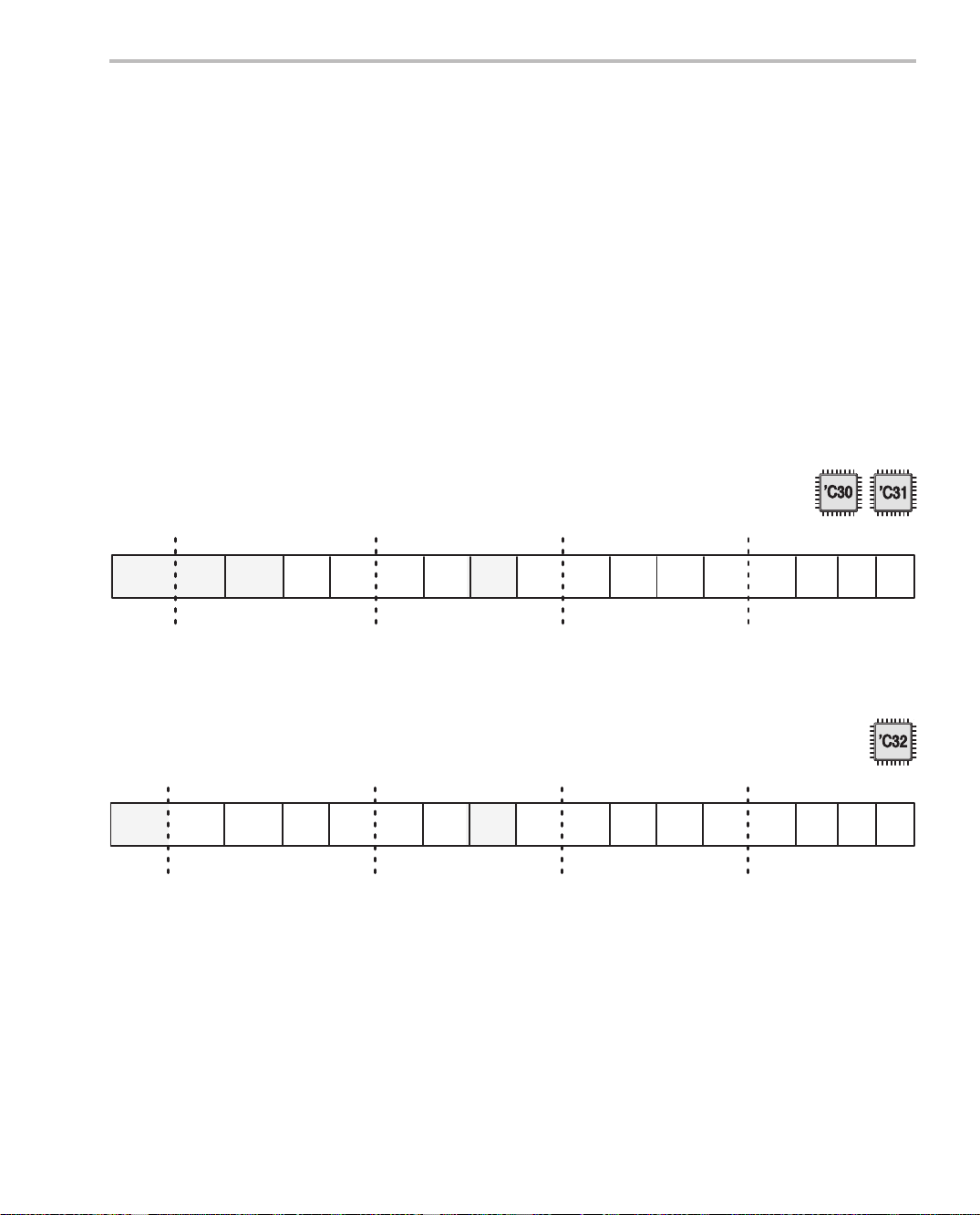
3.1.7 Status (ST) Register
The status (ST) register contains global information about the state of the CPU.
Operations usually set the condition flags of the status register according to
whether the result is 0, negative, etc. This includes register load and store
operations as well as arithmetic and logical functions. However, when the
status register is loaded, the contents of the source operand replace the ST’s
contents bit for bit, regardless of the state of any bits in the source operand.
Following an ST load, the contents of the status register are identical to the
contents of the source operand. This allows the status register to be saved
easily and restored. At system reset, a 0 is written to this register.
Figure 3–3 shows the format of the status register for the ’C30 and ’C31 devices.
Figure 3–4 shows the format of the status register for the ’C32 device. Table 3–2
describes the status register bits, their names, and their functions.
Figure 3–3. Status Register (TMS320C30 andTMS320C31)
CPU Multiport Register File
31 – 16 15 14 13 12 1 1 10 9 8 7 6 5 4 3 2 1
xx
Notes: 1) xx = reserved bit, read as 0
xx
2) R = read, W = write
GIE CC CE CF xx RM OVM LUF LV UF N Z V
xx
R/W R/W R/W R/WR/W R/W R/W R/W R/WR/W R/W
R/W R/W
Figure 3–4. Status Register (TMS320C32 Only)
31 – 16 15 14 13 12 11 10 9 8 7 6 5 4 3 2 1
PRGW
xx GIE CC CE CF xx RM OVM LUF LV UF N Z V
status
Notes: 1) xx = reserved bit, read as 0
2) R = read, W = write
INT
config
R R/W R/W R/W R/W R/WR/W R/W R/W R/W R/WR/W R/W
R/W R/W
0
C
0
C
CPU Registers
3-5
Page 69

CPU Multiport Register File
Table 3–2. Status Register Bits
Bit Name Reset Value Name Description
C 0 Carry flag Carry condition flag
V 0 Overflow flag Overflow condition flag
Z 0 Zero flag Zero condition flag
N 0 Negative flag Negative condition flag
UF 0 Floating-point under-
flow flag
LV 0 Latched overflow flag Latched overflow condition flag
LUF 0 Latched floating-point
underflow flag
OVM 0 Overflow mode flag Overflow mode flag
RM 0 Repeat mode flag Repeat mode flag
CE 0 Cache enable CE enables or disables the instruction cache.
Floating-point underflow condition flag
Latched floating-point underflow condition flag
The overflow mode flag affects only integer operations.
If OVM = 0, the overflow mode is turned off and integer
results that overflow are treated in no special way.
If OVM = 1, integer results overflowing in the positive
direction are set to the most positive, 2s-complement
number (7FFF FFFFh), and integer results overflowing
in the negative direction are set to the mos t negative
32-bit, 2s-complement number (8000 0000h).
If RM = 1, the PC is modified in either the repeat-block
or repeat-single mode.
Set CE = 1 to enable the cac he, allowing the cache to
be used according to the least recently used (LRU)
stack manipulation.
Set CE = 0 to disable the cache, preventing cache
updates or modifications (no cache fetches can be
made). Cache clearing (CC = 1) is allowed when
CE = 0.
Note: If a load of the status register occurs simultaneously with a CPU interrupt pulse trying to reset GIE, GIE is reset.
3-6
Page 70

CPU Multiport Register File
Table 3–2. Status Register Bits (Continued)
Bit Name DescriptionNameReset Value
CF 0 Cache freeze Enables or disables the instruction cache
Set CF = 1 to freeze the cache (cache is not updated),
including LRU stack manipulation. If the cache is
enabled (CE = 1), fetches from the cache are allowed,
but modification of the cache contents is not allowed.
Cache clearing (CC = 1) is allowed. At reset, this bit
is cleared to 0, but it is set to 1 after reset.
When CF = 0, the cache is automatically updated by
instruction fetches from external memory. Also, when
CF = 0, cache clearing (CC = 1) is allowed.
The following table summarizes the CE and CF bits:
CE
CC 0 Cache clear CC = 1 invalidates all entries in the cache. This bit is
always cleared after it is written to, and is always read
as 0. At reset, 0 is written to this bit.
GIE 0 Global interrupt-enable If GIE = 1, the CPU responds to an enabled interrupt.
If GIE = 0, the CPU does not respond to an enabled
interrupt.
INT config 0 Interrupt configuration
(‘C32 only)
Sets the external interrupt signals INT3 – INT0 for levelor edge-triggered interrupts.
INT Config
CF
Effect
0
0
Cache not enabled
0
1
Cache not enabled
1
0
Cache enabled and not frozen
1
1
Cache enabled but frozen
(cache read only)
Effect
0
1
All the external interrupts (INT3 – INT0)
are configured as level-triggered
interrupts. Multiple interrupts may be
triggered when the signal is active for
a long period of time.
All the external interrupts (INT3 – INT0)
are configured as edge-triggered inter-
rupts. Edge and duration are required
for all interrupts to be recognized.
Note: If a load of the status register occurs simultaneously with a CPU interrupt pulse trying to reset GIE, GIE is reset.
CPU Registers
3-7
Page 71

CPU Multiport Register File
Table 3–2. Status Register Bits (Continued)
Bit Name DescriptionNameReset Value
PRGW Dependent
on PRGW
pin level
Note: If a load of the status register occurs simultaneously with a CPU interrupt pulse trying to reset GIE, GIE is reset.
Program width status
(‘C32 only)
Indicates the status of the external input PRGW pin.
When the signal of the PRGW pin is high, the PRGW
status bit is set to 1, indicating a 16-bit memory width.
The ‘C32 performs two fetches to retrieve a single 32-bit
instruction word. The PRGW bit is a read-only bit, and
can have the following values:
PRG
0
1
Effect
Instruction fetches use one 32-bit external program memory read.
Instruction fetches use two 16-bit external program memory reads.
3-8
Page 72
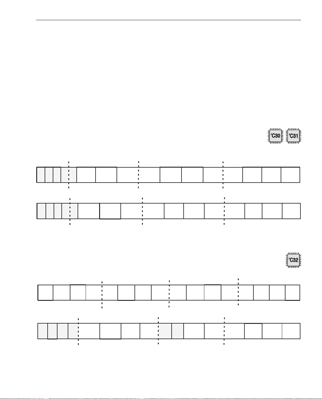
3.1.8 CPU/DMA Interrupt-Enable (IE) Register
The CPU/DMA interrupt-enable (IE) register of the ’C30, ’C31, and ’C32 are
32-bit registers (see Figure 3–5 and Figure 3–6). The CPU interrupt-enable bits
are in locations 10–0 for ’C30 and ’C31 devices, and 11–0 for ’C32 devices. The
direct memory access (DMA) interrupt-enable bits are in locations 26–16 for
‘C30 and ‘C31 devices, and 31–16 for ’C32 devices. A 1 in a CPU/DMA IE bit
enables the corresponding interrupt. A 0 disables the corresponding interrupt.
At reset, 0 is written to this register.
Table 3–3 describes the interrupt-enable register bits, their names, and their
functions.
CPU Multiport Register File
Figure 3–5. CPU/DMA Interrupt-Enable (IE) Register
(TMS320C30 and TMS320C31)
27
xx31xx30xx29xx28xx
xx15xx14xx13xx12xx
26
EDINT
(DMA)
R/W
10
11
EDINT
(CPU)
R/W
25
ETINT1
(DMA)
R/W
ETINT1
(CPU)
R/W
24
ETINT0
(DMA)
R/W
9
ETINT0
(CPU)
R/W
23
ERINT1
(DMA)
R/W
8
ERINT1
(CPU)
R/W
22
EXINT1
(DMA)
R/W
7
EXINT1
(CPU)
R/W
21
ERINT0
(DMA)
R/W
6
5
ERINT0
(CPU)
R/W
20
EXINT0
(DMA)
R/W
4
EXINT0
(CPU)
R/W
19
EINT3
(DMA)
R/W
EINT3
(CPU)
R/W
Notes: 1) xx = reserved bit, read as 0
2) R = read, W = write
Figure 3–6. CPU/DMA Interrupt-Enable (IE) Register (TMS320C32)
31
EINT3
(DMA1)
R/W
30 29 28
EINT1
EINT2
(DMA1)
(DMA1)
R/W
R/W
EINT0
(DMA1)
R/W
27
EDINT0
(DMA1)
R/W
EDINT1
(DMA0)
R/W
25
26
ETINT1
(DMA0)
R/W
24
ETINT0
(DMA0)
R/W
23
ETINT1
(DMA1)
R/W
22
ETINT0
(DMA1)
R/W
21
ERINT0
(DMA1)
R/W
20
EXINT0
(DMA0)
R/W
3
(DMA)
19
EINT3
(DMA0)
R/W
18
EINT2
EINT1
(DMA)
R/W
EINT2
(CPU)
R/W
2
EINT1
(CPU)
R/W
18
EINT2
(DMA0)
R/W17R/W R/W
17
1
R/W
EINT1
(DMA0)
16
EINT0
(DMA)
R/W
EINT0
(CPU)
R/W
16
EINT0
(DMA0)
0
xx15xx14xx13xx
12
11
EDINT1
(CPU)
R/W
10
EDINT0
(CPU)
R/W
Notes: 1) xx = reserved bit, read as 0
2) R = read, W = write
9
ETINT1
(CPU)
R/W
8
ETINT0
(CPU)
R/W
6
xx7xx
R/W
5
ERINT0
(CPU)
R/W
4
EXINT0
(CPU)
R/W
3
EINT3
(CPU)
R/W
2
EINT2
(CPU)
R/W
CPU Registers
1
EINT1
(CPU)
R/W
0
EINT0
(CPU)
R/W
3-9
Page 73

CPU Multiport Register File
Table 3–3. IE Bits and Functions
Reset
Abbreviation
EINT0 (CPU) 0 CPU external interrupt 0 enable
EINT1 (CPU) 0 CPU external interrupt 1 enable
EINT2 (CPU) 0 CPU external interrupt 2 enable
EINT3 (CPU) 0 CPU external interrupt 3 enable
EXINT0 (CPU) 0 CPU serial port 0 transmit interrupt enable
ERINT0 (CPU) 0 CPU serial port 0 receive interrupt enable
EXINT1 (CPU) 0 CPU serial port 1 transmit interrupt enable (’C30 only)
ERINT1 (CPU) 0 CPU serial port 1 receive interrupt enable (’C30 only)
ETINT0 (CPU) 0 CPU timer0 interrupt enable
ETINT1 (CPU) 0 CPU timer1 interrupt enable
EDINT (CPU) 0 CPU DMA controller interrupt enable
Value
Description
(’C30 and ’C31 only)
EDINT0 (CPU) 0 CPU DMA0 controller interrupt enable (’C32 only)
EDINT1 (CPU) 0 CPU DMA1 controller interrupt enable (’C32 only)
EINT0 (DMA) 0 DMA external interrupt 0 enable (’C30 and ’C31 only)
EINT1 (DMA) 0 DMA external interrupt 1 enable (’C30 and ’C31 only)
EINT2 (DMA) 0 DMA external interrupt 2 enable (’C30 and ’C31 only)
EINT3 (DMA) 0 DMA external interrupt 3 enable (’C30 and ’C31 only)
EINT0 (DMA0) 0 DMA0 external interrupt 0 enable (’C32 only)
EINT1 (DMA0) 0 DMA0 external interrupt 1 enable (’C32 only)
EINT2 (DMA0) 0 DMA0 external interrupt 2 enable (’C32 only)
EINT3 (DMA0) 0 DMA0 external interrupt 3 enable (’C32 only)
EXINT0 (DMA) 0 DMA serial port 0 transmit interrupt enable
(’C30 and ’C31 only)
ERINT0 (DMA) 0 DMA serial port 0 receive interrupt enable
(’C30 and ’C31 only)
EXINT1 (DMA) 0 DMA serial port 1 transmit interrupt enable (’C30 only)
ERINT1 (DMA) 0 DMA serial port 1 receive interrupt enable (’C30 only)
EXINT0 (DMA0) 0 DMA0 serial port 1 transmit interrupt enable (’C32 only)
ERINT0 (DMA1)
0 DMA1 serial port 1 receive interrupt enable (’C32 only)
3-10
Page 74

CPU Multiport Register File
Table 3–3. IE Bits and Functions(Continued)
Reset
Abbreviation Description
ETINT0 (DMA) 0 DMA timer0 interrupt enable (’C30 and ’C31)
ETINT1 (DMA) 0 DMA timer1 interrupt enable (’C30 and ’C31 only)
ETINT0 (DMA0) 0 DMA0 timer1 interrupt enable (’C32 only)
ETINT1 (DMA0) 0 DMA0 timer1 interrupt enable (’C32 only)
ETINT0 (DMA1) 0 DMA1 timer0 interrupt enable (’C32 only)
ETINT1 (DMA1) 0 DMA1 timer1 interrupt enable (’C32 only)
EDINT (DMA) 0 DMA controller interrupt enable (’C30 and ’C31 only)
EDINT1 (DMA0) 0 DMA0-DMA1 controller interrupt enable (’C32 only)
EDINT0 (DMA1) 0 DMA1-DMA0 controller interrupt enable (’C32 only)
EINT0 (DMA1) 0 DMA1 external interrupt 0 enable (’C32 only)
EINT1 (DMA1) 0 DMA1 external interrupt 1 enable (’C32 only)
EINT2 (DMA1) 0 DMA1 external interrupt 2 enable (’C32 only)
Value
EINT3 (DMA1)
3.1.9 CPU Interrupt Flag (IF) Register
Figure 3–7, Figure 3–8, and Figure 3–9 show the 32-bit CPU interrupt flag registers (IF) for the ‘C30, ‘C31, and ‘C32 devices, respectively. A 1 in a CPU IF
register bit indicates that the corresponding interrupt is set. The IF bits are set
to 1 when an interrupt occurs. They may also be set to 1 through software to
cause an interrupt. A 0 indicates that the corresponding interrupt is not set. If
a 0 is written to an IF register bit, the corresponding interrupt is cleared. At reset,
0 is written to this register. Table 3–4 describes the interrupt flag register bits,
their names, and their functions.
0 DMA1 external interrupt 2 enable (’C32 only)
CPU Registers
3-11
Page 75

CPU Multiport Register File
Figure 3–7. TMS320C30 CPU Interrupt Flag (IF) Register
10
xx
Notes: 1) xx = reserved bit, read as 0
yy yy
R/W R/W R/W R/W R/W R/W R/W R/W R/W R/W R/W R/W
2) yy = reserved bit, set to 0 at reset; can store value
3) R = read, W = write
DINT9TINT18TINT0
71115–1231–16
XINT1RINT1
5
60
RINT04XINT03INT32INT21INT1
Figure 3–8. TMS320C31 CPU Interrupt Flag (IF) Register
10
xx
Notes: 1) xx = reserved bit, read as 0
yy yy
2) yy = reserved bit, set to 0 at reset
3) R = read, W = write
DINT9TINT18TINT0
R/W R/W R/W R/W R/W R/W R/W R/W R/W R/W R/W
71115–1231–16
xx
xx
5
60
RINT04XINT03INT32INT21INT1
Figure 3–9. TMS320C32 CPU Interrupt Flag (IF) Register
INT0
INT0
31–16
ITTP
Notes: 1) xx = reserved bit, read as 0
2) R = read, W = write
3-12
1115–12
DINT1xx xx
R/W R/W R/W R/W R/W R/W R/W R/W R/W R/W R/W R/W
10
DINT09TINT18TINT0
7
5
6
RINT04XINT03INT32INT21INT1xx
0
INT0
Page 76

CPU Multiport Register File
Table 3–4. IF Bits and Functions
Bit
Name
INT0 0 External interrupt 0 flag
INT1 0 External interrupt 1 flag
INT2 0 External interrupt 2 flag
INT3 0 External interrupt 3 flag
XINT0 0 Serial port 0 transmit flag
RINT0 0 Serial port 0 receive flag
XINT1 0 Serial port 1 transmit flag (‘C30 only)
RINT1 0 Serial port 1 receive interrupt flag (‘C30 only)
TINT0 0 Timer 0 interrupt flag
TINT1 0 Timer 1 interrupt flag
DINT 0 DMA channel interrupt flag (‘C30 and ‘C31 only)
Reset
Value
Function
DINT0 0 DMA0 channel interrupt flag (‘C32 only)
DINT1 0 DMA1 channel interrupt flag (‘C32 only)
ITTP 0 Interrupt-trap table pointer (see Section 3.1.9.1)
Allows the relocation of interrupt and trap vector tables (‘C32 only)
Note: If a load of the interrupt flag (IF) register occurs simultaneously with a set of a flag by an
interrupt pulse, the loading of the flag has higher priority and overwrites the value of the
interrupt flag register.
CPU Registers
3-13
Page 77

CPU Multiport Register File
3.1.9.1 Interrupt-Trap Table Pointer (ITTP)
Similar to the rest of the ‘C3x device family, the ’C32’ s reset vector location
remains at address 0. However, the interrupt and trap vectors are relocatable.
This is achieved by the interrupt-trap table pointer (ITTP) bit field in the CPU
interrupt flag register, shown in Figure 3–9. The ITTP bit field dictates the
starting location (base) of the interrupt-trap vector table. This base address
is formed by left shifting by eight bits the value of the ITTP bit field. This shifted
value is called the effective base address and is referenced as EA[ITTP], as
shown in Figure 3–10. Therefore, the location of an interrupt or trap vector
is given by the addition of the effective base address formed by the ITTP bit
field (EA[ITTP]) and the offset of the interrupt or trap vector in the interrupttrap vector table, as shown in Figure 3–1 1. For example, if the ITTP contains
the value 100h, the serial port transmit interrupt vector is located at 10005h.
Note that the vectors stored in the interrupt-trap vector table are the addresses
of the start of the respective interrupt and trap routines. Furthermore, the
interrupt-trap vector table must lie on a 256-word boundary, since the eight
LSBs of the ef fective base address of the interrupt-trap vector table are 0.
See Section 7.6,
Interrupts
, on page 7-26 for more information on interrupt
vector tables.
Figure 3–10. Effective Base Address of the Interrupt-Trap Vector Table
EA[ITTP] =
Bits 31–16 of the CPU interrupt flag register
70823
00000000
3-14
Page 78

Figure 3–11. Interrupt and Trap Vector Locations
CPU Multiport Register File
EA (ITTP) + 00h
EA (ITTP) + 01h
EA (ITTP) + 02h
EA (ITTP) + 03h
EA (ITTP) + 04h
EA (ITTP) + 05h
EA (ITTP) + 06h
EA (ITTP) + 07h
EA (ITTP) + 08h
EA (ITTP) + 09h
EA (ITTP) + 0Ah
EA (ITTP) + 0Ch
EA (ITTP) + 0Dh
EA (ITTP) + 1Fh
Reserved
INT0
INT1
INT2
INT3
XINT0
RINT0
Reserved
Reserved
TINT0
TINT1
DINT0EA (ITTP) + 0Bh
DINT1
Reserved
EA (ITTP) + 20h TRAP0
.
.
.
.
EA (ITTP) + 3Bh
EA (ITTP) + 3Ch
EA (ITTP) + 3Dh
EA (ITTP) + 3Eh
EA (ITTP) + 3Fh
TRAP27
TRAP28 (reserved)
TRAP29 (reserved)
TRAP30 (reserved)
TRAP31 (reserved)
CPU Registers
3-15
Page 79

CPU Multiport Register File
3.1.10 I/O Flag (IOF) Register
The I/O flag (IOF) register is shown in Figure 3–12 and controls the function
of the dedicated external pins, XF0 and XF1. These pins can be configured for
input or output. The pins can also be read from and written to. At reset, 0 is
written to this register. Table 3–5 describes the I/O flags register bits, their
names, and their functions.
Figure 3–12. I/O Flag (IOF) Register
31–16
Notes: 1) xx = reserved bit, read as 0
15–12
xx xxxx
2) R = read, W = write
11–8
INXF17OUTXF16I
Table 3–5. IOF Bits and Functions
Bit Name
I/OXF0 0 If 0, XF0 is configured a general-purpose input pin.
OUTXF0 0 Data output on XF0.
INXF0 0 Data input on XF0. A write has no effect.
I
/OXF1 0 If 0, XF1 is configured a general-purpose input pin.
OUTXF1 0 Data output on XF1.
INXF1
5
/OXF1
R R/W R/W R R/W R/W
4
INXF03OUTXF02I/OXF01xx
xx
Reset
Value
Function
If 1, XF0 is configured a general-purpose output pin.
If 1, XF1 is configured a general-purpose output pin.
0 Data input on XF1. A write has no effect.
0
3-16
Page 80

CPU Multiport Register File
3.1.11 Repeat-Counter (RC) and Block-Repeat (RS, RE) Registers
The repeat-counter (RC) register is a 32-bit register that specifies the number
of times a block of code is to be repeated when a block repeat is performed.
n
If RC contains the number
The 32-bit repeat start-address (RS) register contains the starting address of
the program-memory block to be repeated when the CPU is operating in the
repeat mode.
The 32-bit repeat end-address (RE) register contains the ending address of
the program-memory block to be repeated when the CPU is operating in the
repeat mode.
Note: RE < RS
If RE< RS and the block mode is enabled, the code between RE and RS is
bypassed when the program counter encounters the repeat end (RE) address.
, the loop is executed n + 1 times.
CPU Registers
3-17
Page 81

Other Registers
3.2 Other Registers
3.2.1 Program-Counter (PC) Register
The program counter (PC) is a 32-bit register containing the address of the
next instruction fetch. While the program-counter register is not part of the
CPU register file, it can be modified by instructions that modify the program
flow.
3.2.2 Instruction Register (IR)
The instruction register (IR) is a 32-bit register that holds the instruction opcode during the decode phase of the instruction. This register is used by the
instruction decode control circuitry and is not accessible to the CPU.
3-18
Page 82

3.3 Reserved Bits and Compatibility
T o retain compatibility with future members of the ’C3x family of microprocessors,
reserved bits that are read as 0 must be written as 0. You must not modify the
current value of a reserved bit that has an undefined value. In other cases, you
should maintain the reserved bits as specified.
Reserved Bits and Compatibility
CPU Registers
3-19
Page 83

Chapter 4
Memory and the Instruction Cache
The ’C3x provides a total memory space of 16M (million) 32-bit words that contain
program, data, and I/O space. Two RAM blocks of 1K 32 bits each (available
on the ’C30 and ’C31) or two RAM blocks of 256 32 bits (available on the ’C32)
and a ROM block of 4K 32 bits (available only on the ’C30) or boot loader
(available on the ’C31 and the ’C32) permit two CPU accesses in a single cycle.
A 64 32-bit instruction cache stores often-repeated sections of code, greatly
reducing the number of off-chip accesses and allowing code to be stored off-chip
in slower, lower-cost memories.
Topic Page
4.1 Memory 4-2. . . . . . . . . . . . . . . . . . . . . . . . . . . . . . . . . . . . . . . . . . . . . . . . . . . . . .
4.2 Reset/Interrupt/Trap Vector Map 4-14. . . . . . . . . . . . . . . . . . . . . . . . . . . . . . .
4.3 Instruction Cache 4-19. . . . . . . . . . . . . . . . . . . . . . . . . . . . . . . . . . . . . . . . . . . .
4-1
Page 84

Memory
4.1 Memory
4.1.1 Memory Maps
The ’C3x accesses a total memory space of 16M (million) 32-bit words of program, data, and I/O space and allows tables, coefficients, program code, or
data to be stored in either RAM or ROM. In this way , you can maximize memory
usage and allocate memory space as desired.
RAM blocks 0 and 1 are each 1K 32 bits on the ’C30 and ’C31. The ROM
block is 4K 32 bits on the ’C30. The ’C31 and ’C32 have a boot ROM. By
manipulating one external pin (MC/MP
or MCBL/MP), you can configure the first
1000h words of memory to address the on-chip ROM or external RAM. Each onchip RAM and ROM block can support two CPU accesses in a single cycle. The
separate program buses, data buses, and DMA buses allow for parallel program
fetches, data reads/writes, and DMA operations, which are covered in Chap ter 1 1,
Peripherals
.
The following sections describe the memory maps for the ’C30, ’C31, and
’C32.
4.1.1.1 TMS320C30 Memory Map
The memory map depends on whether the processor is running in microprocessor mode (MC/MP = 0) or microcomputer mode (MC/MP = 1). The
memory maps for these modes are similar (see Figure 4–1 on page 4-4).
Locations 800000h–801FFFh are mapped to the expansion bus. When this
region is accessed, MSTRB is active. Locations 802000h–803FFFh are
reserved. Locations 804000h–805FFFh are mapped to the expansion bus.
When this region is accessed, IOSTRB
807FFFh are reserved. All of the memory-mapped peripheral bus registers
are in locations 808000h–8097FFh. In both modes, RAM block 0 is located
at addresses 809800h–809BFFh, and RAM block 1 is located at addresses
809C00h–809FFFh. Locations 80A000h–0FFFFFFh are accessed over the
external memory port (STRB
-
Microprocessor Mode
In microprocessor mode, the 4K on-chip ROM is not mapped into the ’C3x
memory map. Locations 0h–03Fh consist of interrupt vector, trap vector,
and reserved locations, all of which are accessed over the external memory
port (STRB
040h–7FFFFFh are also accessed over the external memory port.
is active. Locations 806000h–
active).
active) (see Figure 4–1 on page 4-4). Locations
4-2
Page 85

-
Microcomputer Mode
In microcomputer mode, the 4K on-chip ROM is mapped into locations
0h–0FFFh. There are 192 locations (0h–0BFh) within this block for interrupt
vectors, trap vectors, and a reserved space (’C30). Locations 1000h–
7FFFFFh are accessed over the external memory port (STRB active).
Memory
Se ct i on 4 . 1. 2,
memory maps in greater detail and Section 4.2,
Peripheral Bus Memory Map
, on page 4-9 describes the peripheral
Reset/Interrupt/T rap Vector Map
on page 4-14 provides the vector locations for reset, interrupts, and traps.
Be careful! Access to a reserved area produces unpredictable
results.
,
Memory and the Instruction Cache
4-3
Page 86
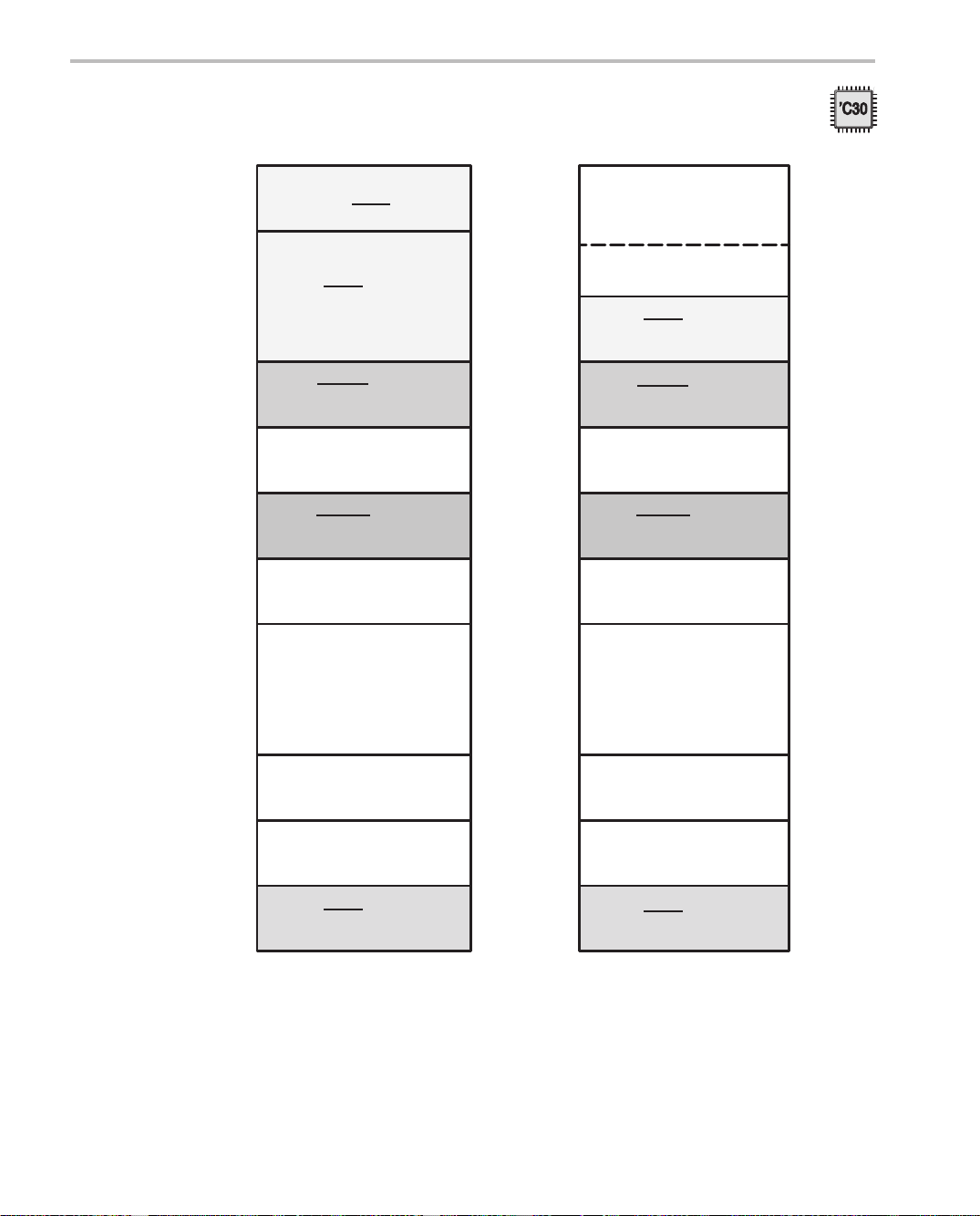
Memory
Figure 4–1. TMS320C30 Memory Maps
0h
03Fh
040h
7FFFFFh
800000h
801FFFh
802000h
803FFFh
804000h
805FFFh
806000h
807FFFh
808000h
8097FFh
809800h
809BFFh
809C00h
809FFFh
80A000h
FFFFFFh
Reset, interrupt, trap vectors,
and reserved locations (64)
(external STRB
STRB active
(8.192M words)
Expansion bus
MSTRB active
(8K words)
Reserved
(8K words)
Expansion bus
IOSTRB
(8K words)
Reserved
(8K words)
Peripheral bus
memory-mapped
(6K words internal)
RAM block 0
(1K words internal)
RAM block 1
(1K words internal)
STRB active
(7.96M words)
Microprocessor mode Microcomputer mode
active)
External
active
registers
External
0h
0BFh
0C0h
0FFFh
1000h
7FFFFFh
800000h
801FFFh
802000h
803FFFh
804000h
805FFFh
806000h
807FFFh
808000h
8097FFh
809800h
809BFFh
809C00h
809FFFh
80A000h
FFFFFFh
Reset, interrupt, trap vectors,
and reserved locations (192)
ROM
(Internal)
External
active
STRB
(8.188M words)
Expansion bus
MSTRB
active
(8K words)
Reserved
(8K words)
Expansion bus
IOSTRB
memory-mapped
(6K words internal)
(1K words internal)
(1K words internal)
active
(8K words)
Reserved
(8K words)
Peripheral bus
registers
(Internal)
RAM block 0
RAM block 1
External
STRB
active
(7.96M words)
4-4
Page 87

4.1.1.2 TMS320C31 Memory Map
The memory map depends on whether the processor is running in microprocessor mode (MCBL/MP = 0) or microcomputer mode (MCBL/MP = 1). The
memory maps for these modes are similar (see Figure 4–2 on page 4-6).
Locations 800000h–807FFFh are reserved. All of the memory-mapped
peripheral bus registers are in locations 808000h–8097FFh. In both modes,
RAM block 0 is located at addresses 809800h–809BFFh, and RAM block 1 is
located at addresses 809C00h–809FFFh. Locations 80A000h–0FFFFFFh
are accessed over the external memory port (STRB
-
Microprocessor Mode
In microprocessor mode, the boot loader is not mapped into the ’C3x
memory map. Locations 0h–03Fh consist of interrupt vector, trap vector,
and reserved locations, all of which are accessed over the external
memory port (STRB active) (see Figure 4–2 on page 4-6). Locations
040h–7FFFFFh are also accessed over the external memory port.
-
Microcomputer Mode
In microcomputer mode, the boot loader ROM is mapped into locations
0h–0FFFh. The last 63 words (809FC1h to 809FFFh) of internal RAM
Block 1 are used for interrupt and trap
4-6). Locations 1000h–7FFFFFh are accessed over the external
memory port (STRB active).
branches
Memory
active).
(see Figure 4–2 on page
Section 4.1.2,
peripheral memory maps in greater detail and Section 4.2,
Trap Vector Map
Peripheral Bus Memory Map
, on page 4-9 describes the
Reset/Interrupt/
, on page 4-14 provides the vector locations for reset, inter-
rupts, and traps.
Be careful! Access to a reserved area produces unpredictable
results.
Memory and the Instruction Cache
4-5
Page 88
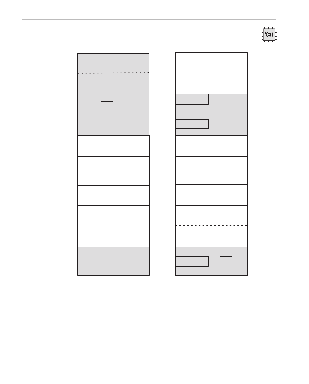
Memory
Figure 4–2. TMS320C31 Memory Maps
0h
03Fh
040h
7FFFFFh
800000h
807FFFh
808000h
8097FFh
809800h
809BFFh
809C00h
809FFFh
80A000h
FFFFFFh
Reset, interrupt, trap vectors,
and reserved locations (64)
(external STRB
STRB active
(8.192M words)
Reserved
(32K words)
Peripheral bus
memory-mapped
(6K words internal)
RAM block 0
(1K words internal)
RAM block 1
(1K words internal)
STRB
(7.96M words)
active)
External
registers
External
active
0h
0FFFh
1000h
400000h
7FFFFFh
800000h
807FFFh
808000h
8097FFh
809800h
809BFFh
809C00h
809FC0h
809FC1h
809FFFh
80A000h
FFF000h
FFFFFFh
Reserved for bootloader operations
Boot 1
Boot 2
Reserved
(32K words)
Peripheral bus
memory-mapped
(6K words internal)
RAM block 0
(1K words internal)
RAM block 1
(1K – 63 words internal)
User program interrupt
and trap branches
(63 words internal)
Boot 3
External
STRB
active
(8.188M words)
registers
External
STRB
active
(7.96M words)
†
4-6
Microprocessor mode Microcomputer/boot-loader mode
†
See Section 3.1.3,
Data-Page Pointer (DP)
, on page 3-4 for more information.
Page 89

4.1.1.3 TMS320C32 Memory Map
The memory map depends on whether the processor is running in microprocessor mode (MCBL/MP = 0) or microcomputer mode (MCBL/MP = 1). The
memory maps for these modes are similar (see Figure 4–3 on page 4-8).
Locations 800000h–807FFFh, 809800h–80FFFh, and 830000H–87FDFFh are
reserved. Locations 810000h–82FFFFh are mapped to the external bus with
IOSTRB
active. All of the memory-mapped peripheral bus registers are in locations 808000h–8097FFh. In both modes, RAM block 0 is located at addresses
87FE00h–87FEFFh, and RAM block 1 is located at addresses 87FF00h–
87FFFFh. Locations 900000h–FFFFFFh are mapped to the external bus with
STRB1 active.
Unlike the fixed interrupt-trap vector table location of the ’C30 and ’C31 devices,
the ’C32 has a user-relocatable interrupt-trap vector table. The interrupt-trap
vector table must start on a 256-word boundary. The starting location is programmed through the interrupt-trap table pointer (ITTP) bit field in the CPU interrupt flag (IF) register. See Section 3.1.9.1,
on page 3-14.
-
Microprocessor Mode
Memory
Interr up t- Trap Table Pointer (I TT P )
,
In microprocessor mode, the boot loader is not mapped into the ’C3x memory
map. Locations 0h–7FFFFFFh are accessed over the external memory port
(STRB0 active) with location 0h containing the reset vector.
-
Microcomputer Mode
In microcomputer mode, the on-chip boot loader ROM is mapped into
locations 0h–0FFFh. Locations 1000h–7FFFFFh are accessed over the
external memory port (STRB0 active).
The ’C32 boot loader has additional modes over the ’C31 boot loader to handle
the data types, sizes, and memory widths supported by the external memory interface. The memory boot load supports data transfer with and without handshaking.
The handshake mode allows synchronous program transfer by using two pins as
data-acknowledge and data-ready signals.
See Section 4.1.2,
Reset/Interrupt/Trap Vector Map
Peripheral Bus Memory Map
, on page 4-14 for more information.
, on page 4-9 and Section 4.2,
Be careful! Access to a reserved area produces unpredictable
results.
Memory and the Instruction Cache
4-7
Page 90

Memory
Figure 4–3. TMS320C32 Memory Maps
0h
7FFFFFh
800000h
807FFFh
808000h
8097FFh
809800h
80FFFFh
810000h
Reset-vector location
External memory
memory-mapped registers
(6K words internal)
External memory
IOSTRB
active
STRB0
(8.192M words)
Reserved
(32K words)
Peripheral bus
Reserved
(26K words)
active (128K)
(128K words)
0h
0FFFh
1000h
1001h
7FFFFFh
800000h
807FFFh
808000h
8097FFh
809800h
80FFFFh
810000h
810001h
Reserved for
boot-loader operations
Boot 1
External memory
STRB0
active
(8.188M words)
Reserved
(32K words)
Peripheral bus
memory-mapped registers
(6K words internal)
Reserved
(26K words)
Boot 2
External memory
active (128K)
IOSTRB
(128K words)
4-8
82FFFFh
830000h
87FDFFh
87FE00h
87FEFFh
87FF00h
87FFFFh
880000h
8FFFFFh
900000h
FFFFFFh
82FFFFh
Reserved
(319.5K words)
RAM block 0
(256 words internal)
RAM block 1
(256 words internal)
External memory
STRB0
active
(512K words)
External memory
Microprocessor mode Microcomputer/boot-loadermode
active
STRB1
(7.168M words)
830000h
87FDFFh
87FE00h
87FEFFh
87FF00h
87FFFFh
880000h
8FFFFFh
900000h
900001h
FFFFFFh
Reserved
(319.5K words)
RAM block 0
(256 words internal)
RAM block 1
(256 words internal)
External memory
STRB0
active
(512K words)
Boot 3
External memory
active
STRB1
(7.168M words)
Page 91

4.1.2 Peripheral Bus Memory Map
The following sections describe the peripherial bus memory maps for the ’C30,
’C31, and ’C32.
4.1.2.1 TMS320C30 Peripheral Bus Memory Map
The ’C30 memory-mapped peripheral registers are located starting at address
808000h. Figure 4–4 on page 4-10 shows the peripheral bus memory map. The
shaded blocks are reserved.
Memory
Memory and the Instruction Cache
4-9
Page 92

Memory
Figure 4–4. TMS320C30 Peripheral Bus Memory-Mapped Registers
808000h
808004h
808006h
808008h
808020h
808024h
808028h
808030h
808034h
808038h
808040h
808042h
808043h
808044h
808045h
808046h
808048h
DMA global control
DMA source address
DMA destination address
DMA transfer counter
Timer 0 global control
Timer 0 counter
Timer 0 period
Timer 1 global control
Timer 1 counter
Timer 1 period register
Serial port 0 global control
FSX/DX/CLKX serial port 0 control
FSR/DR/CLKR serial port 0 control
Serial port 0 R/X timer control
Serial port 0 R/X timer counter
Serial port 0 R/X timer period
Serial port 0 data transmit
4-10
80804Ch
808050h
808052h
808053h
808054h
808055h
808056h
808058h
80805Ch
808060h
808064h
Serial port 0 data receive
Serial port 1 global control
FSX/DX/CLKX serial port 1 control
FSR/DR/CLKR serial port 1 control
Serial port 1 R/X timer control
Serial port 1 R/X timer counter
Serial port 1 R/X timer period
Serial port 1 data transmit
Serial port 1 data receive
Expansion-buscontrol
Primary-buscontrol
Page 93

4.1.2.2 TMS320C31 Peripheral Bus Memory Map
The ’C31 memory-mapped peripheral registers are located starting at address
808000h. Figure 4–5 shows the peripheral bus memory map. The shaded
blocks are reserved.
Figure 4–5. TMS320C31 Peripheral Bus Memory-Mapped Registers
Memory
808000h
808004h
808006h
808008h
808020h
808024h
808028h
808030h
808034h
808038h
808040h
808042h
808043h
808044h
808045h
808046h
808048h
DMA global control
DMA source address
DMA destination address
DMA transfer counter
Timer 0 global control
Timer 0 counter
Timer 0 period
Timer 1 global control
Timer 1 counter
Timer 1 period register
Serial port global control
FSX/DX/CLKX serial port control
FSR/DR/CLKR serial port control
Serial port R/X timer control
Serial port R/X timer counter
Serial port R/X timer period
Serial port data transmit
80804Ch
808064h
Serial port data receive
Primary-buscontrol
Memory and the Instruction Cache
4-11
Page 94

Memory
4.1.2.3 TMS320C32 Peripheral Bus Memory Map
The ’C32’s memory-mapped peripheral and external-bus control registers are
located starting at address 808000h, as shown in Figure 4–6 on page 4-13. The
shaded blocks are reserved.
4-12
Page 95

Figure 4–6. TMS320C32 Peripheral Bus Memory-Mapped Registers
Memory
808000h
808004h
808006h
808008h
808010h
808014h
808016h
808018h
808020h
808024h
808028h
808030h
808034h
808038h
808040h
DMA 0 global control
DMA 0 source address
DMA 0 destination address
DMA 0 transfer counter
DMA 1 global control
DMA 1 source address
DMA 1 destination address
DMA 1 transfer counter
Timer 0 global control
Timer 0 counter
Timer 0 period
Timer 1 global control
Timer 1 counter
Timer 1 period register
Serial port global control
808042h
808043h
808044h
808045h
808046h
808048h
80804Ch
808060h
808064h
808068h
8097FFh
FSX/DX/CLKX serial port control
FSR/DR/CLKR serial port control
Serial port R/X timer control
Serial port R/X timer counter
Serial port R/X timer period
Serial port data transmit
Serial port data receive
IOSTRB buscontrol
STRB0 buscontrol
STRB1 buscontrol
Memory and the Instruction Cache
4-13
Page 96

Reset/Interrupt/Trap Vector Map
4.2 Reset/Interrupt/Trap Vector Map
The addresses for the reset, interrupt, and trap vectors are 00h–3Fh, as shown
in Figure 4–7 and Figure 4–8. The reset vector contains the address of the reset
routine.
-
’C30 and ’C31 Microprocessor and Microcomputer Modes
In the microprocessor mode of the ’C30 and ’C31 and the microcomputer
mode of the ’C30, the reset interrupt and trap vectors stored in locations
0h–3Fh are the addresses of the starts of the respective reset, interrupt,
and trap routines. For example, at reset, the content of memory location
00h (reset vector) is loaded into the PC, and execution begins from that
address (see Figure 4–8 on page 4-16).
-
’C31 Microcomputer/Boot-Loader Mode
In the microcomputer/boot-loader mode of the ’C31, the interrupt and trap
vectors stored in locations 809FC1h–809FFFh are
the start of the respective interrupt and trap routines (see Figure 4–9 on
page 4-17).
branch
instructions to
-
’C32 Microprocessor and Microcomputer/Boot-Loader Mode
The ’C32 has a user-relocatable interrupt-trap vector table. The interrupttrap vector table must start on a 256-word boundary . The starting location is
programmed through the interrupt-trap table pointer (ITTP) bit field in the
CPU interrupt flag (IF) register. See Section 3.1.9.1,
Pointer (ITTP)
, on page 3-14. The reset vector is stored at location 0h in
Interrupt-Trap Table
microprocessor mode.
4-14
Page 97
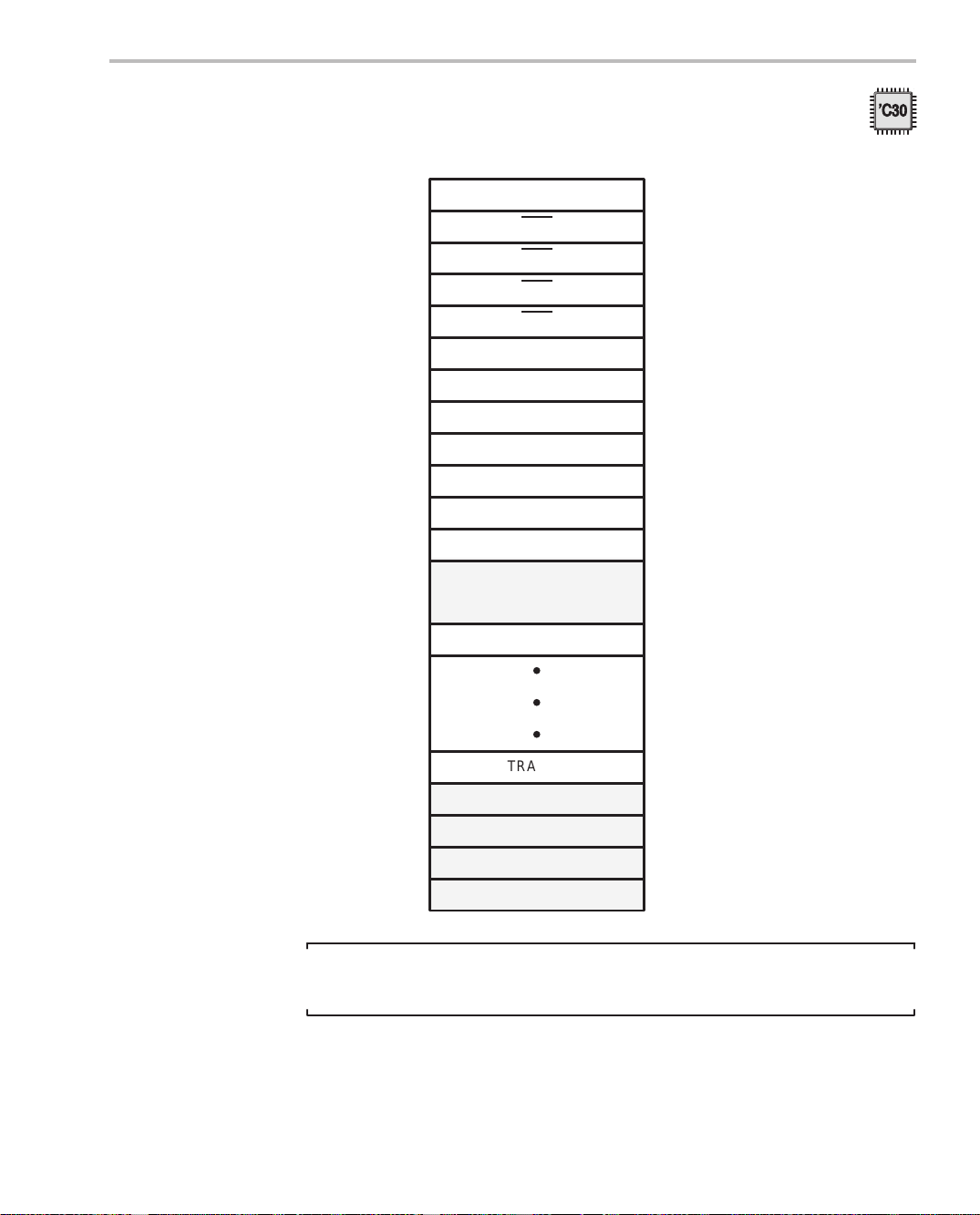
Reset/Interrupt/Trap Vector Map
Figure 4–7. Reset, Interrupt, and Trap Vector Locations for the TMS320C30
Microprocessor Mode
RESET00h
01h
02h
03h
04h
05h
06h
07h
08h
09h
0Ah
0Bh
0Ch
1Fh
20h
INT0
INT1
INT2
INT3
XINT0
RINT0
XINT1
RINT1
TINT0
TINT1
DINT
Reserved
TRAP 0
D
D
D
TRAP 273Bh
3Ch
3Dh
3Eh
3Fh
TRAP 28 (reserved)
TRAP 29 (reserved)
TRAP 30 (reserved)
TRAP 31 (reserved)
Note: Traps 28–31
Traps 28–31 are reserved; do not use them.
Memory and the Instruction Cache
4-15
Page 98
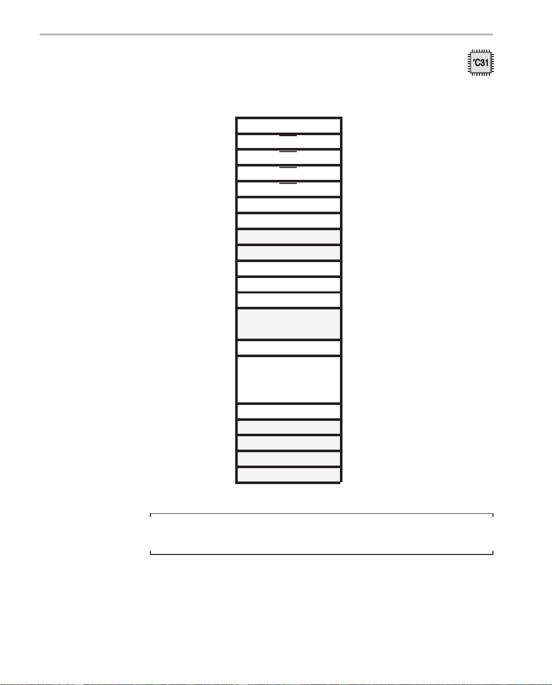
Reset/Interrupt/Trap Vector Map
Figure 4–8. Reset, Interrupt, and Trap Vector Locations for theTMS320C31
Microprocessor Mode
00h RESET
01h INT0
02h INT1
03h INT2
04h INT3
05h XINT0
06h RINT0
07h XINT1 (Reserved)
08h RINT1 (Reserved)
09h TINT0
0Ah TINT1
0Bh DINT
0Ch
1Fh
20h TRAP 0
•
•
3Bh TRAP 27
3Ch TRAP 28 (reserved)
3Dh TRAP 29 (reserved)
3Eh TRAP 30 (reserved)
3Fh TRAP 31 (reserved)
Reserved
•
4-16
Note: Traps 28–31
Traps 28–31 are reserved; do not use them.
Page 99
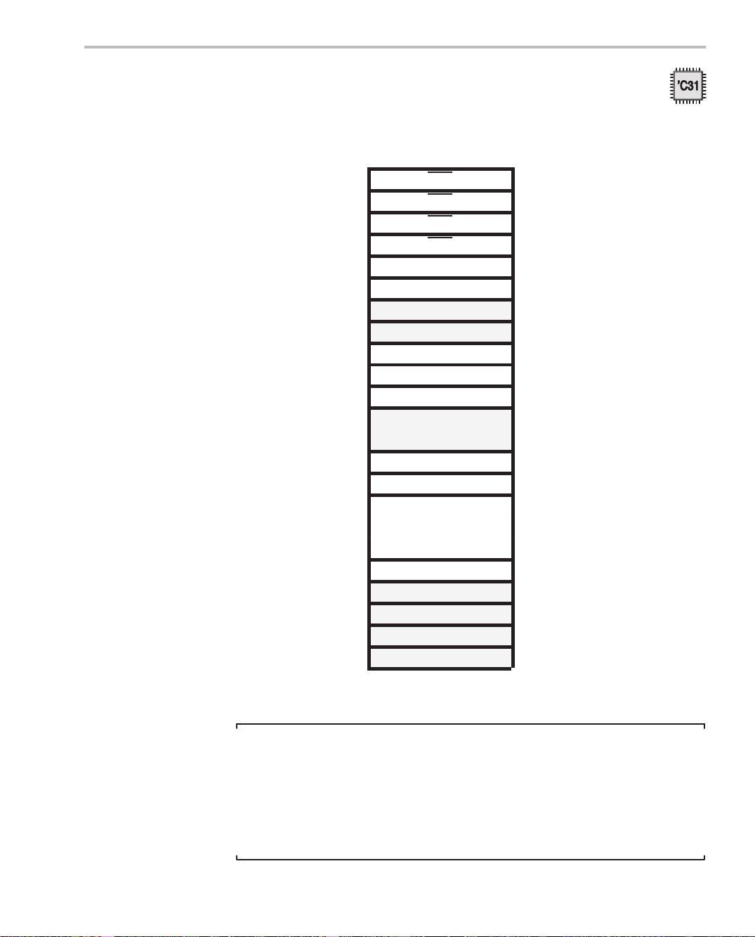
Reset/Interrupt/Trap Vector Map
Figure 4–9. Interrupt and Trap Branch Instructions for the TMS320C31
Microcomputer Mode
809FC1h INT0
809FC2h INT1
809FC3h INT2
809FC4h INT3
809FC5h XINT0
809FC6h RINT0
809FC7h XINT1 (reserved)
809FC8h RINT1 (reserved)
809FC9h TINT0
809FCAh TINT1
809FCBh DINT
809FCCh
809FDFh
809FE0h TRAP 0
809FE1h TRAP 1
•
•
809FFBh TRAP 27
809FFCh TRAP 28 (reserved)
809FFDh TRAP 29 (reserved)
809FFEh TRAP 30 (reserved)
809FFFh TRAP 31 (reserved)
Reserved
•
Note: Traps 28–31
Traps 28–31 are reserved; do not use them.
Unlike the ’C31’s microprocessor mode, the ’C31 microcomputer/boot loader
mode uses a dual-vectoring scheme to service interrupts and trap requests. In
this dual vectoring scheme, a branch instruction rather than a vector address
is used.
Memory and the Instruction Cache
4-17
Page 100
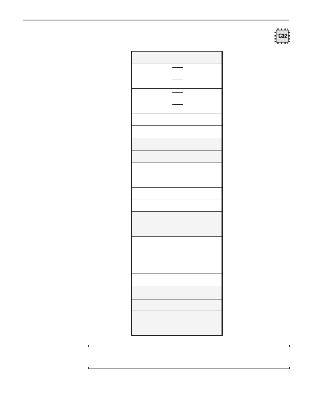
Reset/Interrupt/Trap Vector Map
Figure 4–10. Interrupt and Trap Vector Locations for TMS320C32
EA (ITTP) + 00h
EA (ITTP) + 01h
EA (ITTP) + 02h
EA (ITTP) + 03h
EA (ITTP) + 04h
EA (ITTP) + 05h
EA (ITTP) + 06h
EA (ITTP) + 07h
EA (ITTP) + 08h
EA (ITTP) + 09h
EA (ITTP) + 0Ah
EA (ITTP) + 0Ch
EA (ITTP) + 0Dh
EA (ITTP) + 1Fh
Reserved
INT0
INT1
INT2
INT3
XINT0
RINT0
Reserved
Reserved
TINT0
TINT1
DINT0EA (ITTP) + 0Bh
DINT1
Reserved
4-18
EA (ITTP) + 20h TRAP0
.
.
.
.
EA (ITTP) + 3Bh
EA (ITTP) + 3Ch
EA (ITTP) + 3Dh
EA (ITTP) + 3Eh
EA (ITTP) + 3Fh
TRAP27
TRAP28 (reserved)
TRAP29 (reserved)
TRAP30 (reserved)
TRAP31 (reserved)
Note: Traps 28–31
Traps 28–31 are reserved; do not use them.
 Loading...