

Page 1

现货库存、技术资料、百科信息、热点资讯,精彩尽在鼎好!
D
Based Upon the T320C2xLP Core CPU
D
16-Bit Fixed-Point DSP Architecture
– Six Internal Buses for Increased
Parallelism and Performance
– 32-Bit ALU/Accumulator
– 16 × 16-Bit Single-Cycle Multiplier With a
32-Bit Product
– Block Moves for Data, Program,
I/O Space
– Hardware Repeat Instruction
D
Instruction Cycle Time
’C203 ’LC203 ’C209
50 ns @ 5 V 50 ns @ 3.3 V 50 ns @ 5 V
35 ns @ 5 V 35 ns @ 5 V
25 ns @ 5 V
D
Source Code Compatible With TMS320C25
D
Upwardly Code-Compatible With
TMS320C5x Devices
D
Four External Interrupts
D
Boot-Loader Option (’C203 Only)
D
TMS320C2xx Integrated Memory:
– 544 × 16 Words of On-Chip Dual-Access
Data RAM
– 4K × 16 Words of On-Chip Single-Access
Program/Data RAM (’C209 only)
– 4K × 16 Words of On-Chip Program ROM
(’C209 Only)
D
224K × 16-Bit Total Addressable External
Memory Space
– 64K Program
– 64K Data
– 64K I/O
– 32K Global
description
TMS320C203, TMS320C209, TMS320LC203
DIGITAL SIGNAL PROCESSORS
SPRS025B – JUNE 1995 – REVISED AUGUST 1998
D
TMS320C2xx Peripherals:
– PLL With Various Clock Options
– ×1, ×2, ×4, 2 (’C203)
– ×2, 2 (’C209)
– On-Chip Oscillator
– One Wait State Software-Programmable
to Each Space (’C209 Only)
– 0 – 7 Wait States Software-Programmable
to Each Space (’C203 Only)
– Six General-Purpose I/O Pins
– On-Chip 20-Bit Timer
– Full-Duplex Asynchronous Serial Port
(UART) (’C203 Only)
– One Synchronous Serial Port With
Four-Level-Deep FIFOs (’C203 Only)
D
Supports Hardware Wait States
D
Designed for Low-Power Consumption
– Fully Static CMOS Technology
– Power-Down IDLE Mode
D
1.1 mA/MIPS at 3.3 V
D
’C203 is Pin-Compatible With TMS320F206
Flash DSP
D
Up to 40-MIPS Performance at 5 V (’C203)
D
20-MIPS Performance at 3.3 V
D
HOLD Mode for Multiprocessor
Applications
D
IEEE-1 149.1†-Compatible Scan-Based
Emulation
D
80- and 100-pin Small Thin Quad Flat
Packages (TQFPs), (PN and PZ Suffixes)
The TMS320C2xx generation of digital signal processors (DSPs) combines strong performance and great
flexibility to meet the needs of signal processing and control applications. The T320C2xLP core CPU that is the
basis of all ’C2xx devices has been optimized for high speed, small size, and low-power, making it ideal for
demanding applications in many markets. The CPU has an advanced, modified Harvard architecture with six
internal buses that permits tremendous parallelism and data throughput. The powerful ’C2xx instruction set
makes software development easy . And because the ’C2xx is code-compatible with the TMS320C2x and ’C5x
generations, your code investment is preserved. Around this core, ’C2xx-generation devices feature various
combinations of on-chip memory and peripherals. The serial ports provide easy communication with external
devices such as codecs, A/D converters, and other processors. Other peripherals that facilitate the control of
external devices include general-purpose I/O pins, a 20-bit timer, and a wait-state generator.
Please be aware that an important notice concerning availability, standard warranty, and use in critical applications of
Texas Instruments semiconductor products and disclaimers thereto appears at the end of this data sheet.
†
IEEE Standard 1149.1-1990, IEEE Standard Test-Access Port.
PRODUCTION DATA information is current as of publication date.
Products conform to specifications per the terms of Texas Instruments
standard warranty. Production processing does not necessarily include
testing of all parameters.
POST OFFICE BOX 1443 • HOUSTON, TEXAS 77251–1443
Copyright 1998, Texas Instruments Incorporated
1
Page 2
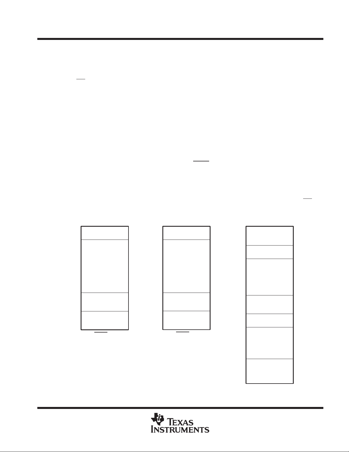
TMS320C203, TMS320C209, TMS320LC203
I/O PORTS
SUPPLY
TIME
TYPE WITH
DIGITAL SIGNAL PROCESSORS
SPRS025B – JUNE 1995 – REVISED AUGUST 1998
description (continued)
Because of their strong performance, low cost, and easy-to-use development environment, ’C2xx-generation
DSPs are an ideal choice for applications such as smart phones, digital cameras, modems, remote metering,
and security systems.
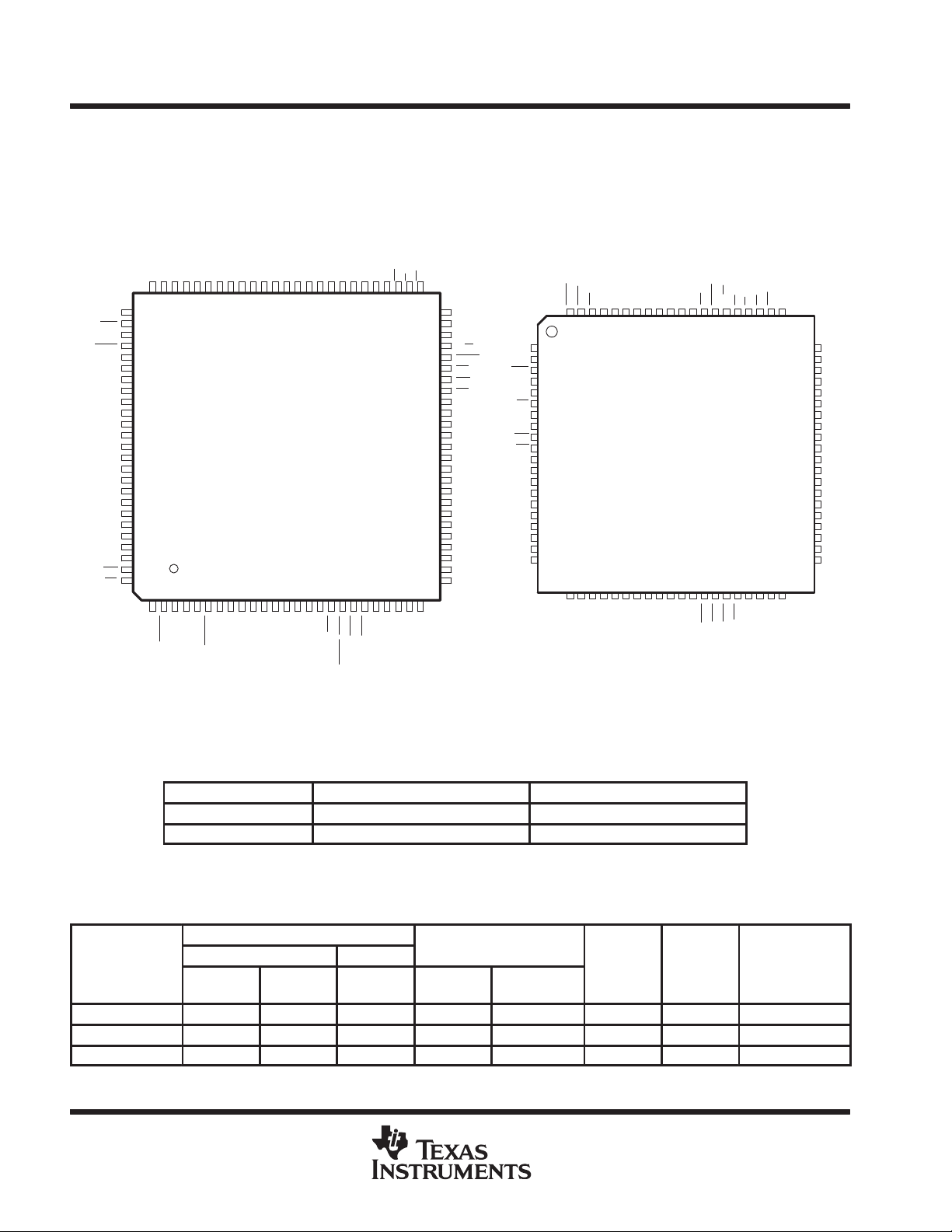
PZ PACKAGE
(TOP VIEW)
PN PACKAGE
(TOP VIEW)
EMU0
EMU1/OFF
TCK
TRST
TDI
TMS
TDO
V
CLKR
FSR
DR
CLKX
V
FSX
DX
V
TOUT
V
RX
IO0
IO1
BIO
RS
A14
A13
A12VA11
DD
DIV1VDIV2
SS
DD
V
HOLDA
SS
A10A9A8VA7VA6A5A4VA3A2A1A0VPSIS
DD
IO2
IO3
V
PLL5V
CLKIN/X2
DD
V
A15
76
77
78
79
80
81
82
83
SS
84
85
86
87
88
SS
89
90
91
DD
92
TX
93
94
SS
95
96
97
XF
98
99
TEST
BOOT
DD
X1
SS
V
CLKOUT1
SS
DD
NMI
V
HOLD /INT1
INT2
INT3
SS
V
SS
D0D1D2
DS
DD
51525354555657585960616263646566676869707172737475
50
V
DD
49
READY
48
V
SS
47
R/W
46
STRB
45
RD
44
WE
43
BR
42
V
SS
41
D15
40
D14
39
D13
38
D12
37
V
SS
36
D11
35
V
DD
34
D10
33
D9
32
D8
31
D7
V
30
SS
D6
29
D5
28
D4
27
D3
26100
25242322212019181716151413121110987654321
SS
V
V
EMU0
EMU1/OFF
TDI
READY
TCK
BIO
MP/MC
D15
V
D14
D13
V
D12
D11
D10
DD
RS
RS
SS
DD
D9
D8
TRST
IACKRDV
77
78
79
80
1
2
3
4
5
6
7
8
9
10
11
12
13
14
15
16
17
18
19
20
24
23
22
21
D7D6D5D4D3SSD1
SS
SS
V
V
XF
CLKOUT1
75
76
26
25
SS
V
TOUT
CLKMOD
72
73
74
29
28
27
D2
V
TDO
71
30
X1
CLKIN/X2
69
70
32
31
D0
TMS
BR
68
33
INT1
STRB
67
34
INT2
R/W
66
35
INT3
PSISDSWEV
63
64
65
38
37
36
NMI
PLL5V
RAMEN
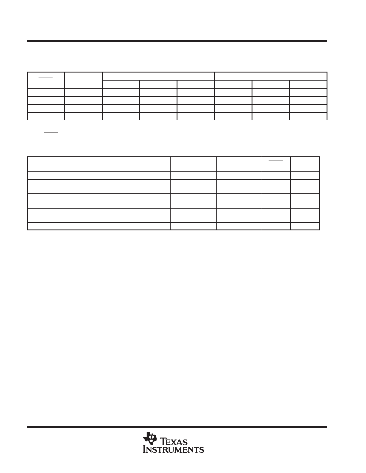
Table 2 provides a comparison of the devices in the ’C2xx generation. It shows the capacity of on-chip RAM
and ROM, the number of serial and parallel I/O ports, the execution time of one machine cycle, and the type
of package with total pin count.
SS
61
62
A15
60
A14
59
A13
58
A12
57
V
56
SS
A11
55
A10
54
A9
53
A8
52
V
51
DD
V
50
DD
A7
49
A6
48
V
47
SS
A5
46
A4
45
A3
44
A2
43
A1
42
V
41
SS
40
39
A0
RES1
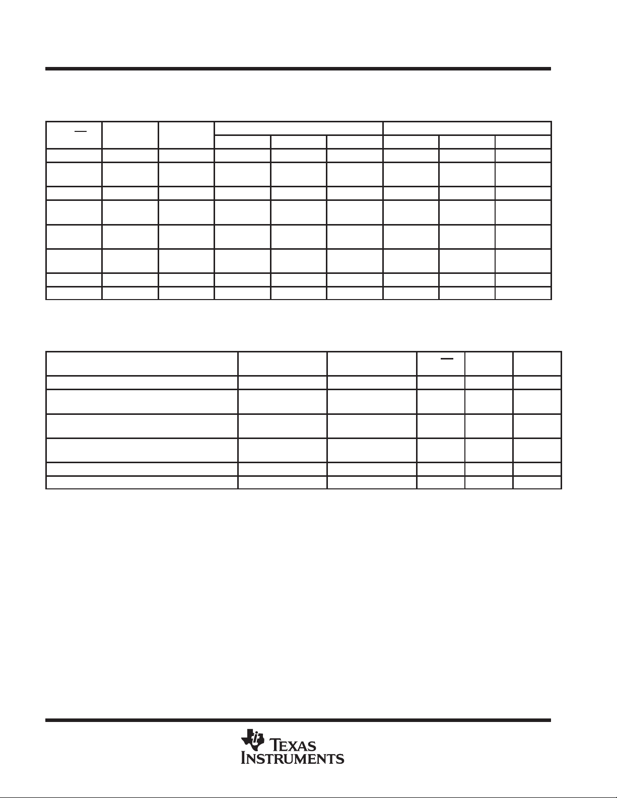
Table 1. Low Power Dissipation
†
POWER TMS320C203 TMS320C209
3.3 V 1.1 mA/MIPS N/A
5 V 1.9 mA/MIPS 1.9 mA/MIPS
†
Core power dissipation. For complete details, see
Calculation of TMS320C2xx Power Dissipation
(literature
number SPRA088).
Table 2. Characteristics of the TMS320C2xx Processors
ON-CHIP MEMORY
TMS320C2xx
DEVICES
RAM ROM
DATA
DATA/
PROG
PROG SERIAL PARALLEL
TMS320C203 288 256 – 2 64K 5 50/35/25 100-pin TQFP
TMS320C209 288 4K + 256 4K – 64K 5 50/35 80-pin TQFP
TM320LC203 288 256 – 2 64K 3.3 50 100-pin TQFP
2
POST OFFICE BOX 1443 • HOUSTON, TEXAS 77251–1443
POWER
(V)
CYCLE
(ns)
PACKAGE
PIN COUNT
Page 3
TYPE
†
DESCRIPTION
TMS320C203 and TMS320LC203 Terminal Functions
TERMINAL
NAME NO.
DATA AND ADDRESS BUSES
D15
D14
D13
D12
D11
D10
D9
D8
D7
D6
D5
D4
D3
D2
D1
D0
A15
A14
A13
A12
A11
A10
A9
A8
A7
A6
A5
A4
A3
A2
A1
A0
PS 53 O/Z
DS 51 O/Z
IS 52 O/Z
READY 49 I
R/W 47 O/Z
RD 45 O/Z
WE 44 O/Z
†
I = input, O = output, Z = high impedance, PWR = power, GND = ground
41
40
39
38
36
34
33
32
31
29
28
27
26
24
23
22
74
73
72
71
69
68
67
66
64
62
61
60
58
57
56
55
I/O/Z
O/Z
Parallel data bus D15 [most significant bit (MSB)] through D0 [least significant bit (LSB)]. D15–D0 are
multiplexed to transfer data between the TMS320C2xx and external data/program memory or I/O
devices. Placed in the high-impedance state when not outputting (R/W
go into the high-impedance state when OFF
Parallel address bus A15 (MSB) through A0 (LSB). A15–A0 are multiplexed to address external
data/program memory or I/O devices. These signals go into the high-impedance state when OFF
low.
MEMORY CONTROL SIGNALS
Program-select signal. PS is always high unless low-level asserted for communicating to off-chip program
space. PS
Data-select signal. DS is always high unless low-level asserted for communicating to off-chip program
space. DS
I/O space-select signal. IS is always high unless low-level asserted for communicating to I/O ports. IS
goes into the high-impedance state when OFF is active low.
Data-ready input. READY indicates that an external device is prepared for the bus transaction to be
completed. If the external device is not ready (READY low), the TMS320C203 waits one cycle and checks
READY again. If READY is not used, it should be pulled high.
Read/write signal. R/W indicates transfer direction when communicating to an external device. R/W is
normally in read mode (high), unless low level is asserted for performing a write operation. R/W
the high-impedance state when OFF
Read-select indicates an active, external read cycle and can connect directly to the output enable (OE)
of external devices. RD
high-impedance state when OFF
Write enable. The falling edge of WE indicates that the device is driving the external data bus (D15–D0).
Data can be latched by an external device on the rising edge of WE
data, and I/O writes. WE
goes into the high-impedance state when OFF is active low.
goes into the high-impedance state when OFF is active low.
is active on all external program, data, and I/O reads. RD goes into the
goes into the high-impedance state when OFF is active low.
TMS320C203, TMS320C209, TMS320LC203
DIGITAL SIGNAL PROCESSORS
SPRS025B – JUNE 1995 – REVISED AUGUST 1998
high) or RS when asserted. They
is active low.
is active
goes into
is active low.
is active low.
. WE is active on all external program,
POST OFFICE BOX 1443 • HOUSTON, TEXAS 77251–1443
3
Page 4
TMS320C203, TMS320C209, TMS320LC203
TYPE
†
DESCRIPTION
DIGITAL SIGNAL PROCESSORS
SPRS025B – JUNE 1995 – REVISED AUGUST 1998
TMS320C203 and TMS320LC203 Terminal Functions (Continued)
TERMINAL
NAME NO.
MEMORY CONTROL SIGNALS (CONTINUED)
STRB 46 O/Z
BR 43 O/Z
HOLDA 6 O/Z
XF 98 O/Z
BIO 99 I
IO0
IO1
IO2
IO3
RS 100 I
TEST 1 I Reserved input pin. TEST is connected to VSS for normal operation.
BOOT 2 I
NMI 17 I
HOLD/INT1 18 I
INT2
INT3
TOUT 92 O
CLKOUT1 15 O/Z
CLKIN/X2
X1
DIV1
DIV2
†
I = input, O = output, Z = high impedance, PWR = power, GND = ground
96
97
19
20
12
13
I/O/Z
8
9
3
5
Strobe signal. STRB is always high unless asserted low to indicate an external bus cycle. STRB goes into the
high-impedance state when OFF
MULTI-PROCESSING SIGNALS
Bus-request signal. BR is asserted when a global data-memory access is initiated. BR goes into the
high-impedance state when OFF
Hold-acknowledge signal. HOLDA indicates to the external circuitry that the processor is in a hold state and
that the address, data, and memory control lines are in the high-impedance state so that they are available to
the external circuitry for access of local memory. HOLDA
active low.
External flag output (latched software-programmable signal). XF is used for signalling other processors in
multiprocessing configurations or as a general-purpose output pin. XF goes into the high-impedance state
when OFF
Branch control input. When polled by the BIOZ instruction, if BIO is low, the TMS320C203 executes a
branch. If BIO
Software-controlled input/output pins by way of the asynchronous serial-port control register (ASPCR). At
reset, IO0–IO3 are configured as inputs. These pins can be used as general-purpose input/output pins or as
handshake control for the UART. IO0–IO3 go into the high-impedance state when OFF
Reset input. RS causes the TMS320C203 to terminate execution and forces the program counter to zero.
When RS
various registers and status bits.
Microprocessor-mode-select pin. When BOOT is high, the device accesses off-chip memory. If BOOT is low ,
the on-chip boot-loader transfers data from external global data space to external RAM program space.
Nonmaskable interrupt. NMI is an external interrupt that cannot be masked by way of the interrupt-mode bit
(INTM) or the interrupt mask register (IMR). When NMI
vector location. If NMI
HOLD and INT1 share the same pin. Both are treated as interrupt signals. If the MODE bit is 0 in the
interrupt-control register (ICR), hold logic can be implemented in combination with the IDLE instruction in
software. At reset, the MODE bit in ICR is zero, enabling the HOLD mode for the pin.
External user interrupts. INT2 and INT3 are prioritized and maskable by the IMR and the INTM. INT2 and INT3
can be polled and reset by way of the interrupt flag register (IFR). If these signals are not used, they should
I
be pulled high.
Timer output. TOUT signals a pulse when the on-chip timer counts down past zero. The pulse is one
CLKOUT1-cycle wide. TOUT goes into the high-impedance state when OFF
Master clock ouput signal. The CLKOUT1 high pulse signifies the logic phase while the low pulse signifies the
latch phase.
Input clock. CLKIN/X2 is the input clock to the device. As CLKIN, the pin operates as the external oscillator
I
clock input, and as X2, the pin operates as the internal oscillator input with X1 being the internal oscillator
O
output.
DIV1 and DIV2 provide clock-mode inputs.
I
DIV1–DIV2 should not be changed unless the RS
is active low.
is not used, it should be pulled high.
INITIALIZATION, INTERRUPTS, AND RESET OPERATIONS
is brought high, execution begins at location 0 of program memory after 16 cycles. RS affects
is not used, it should be pulled high.
OSCILLATOR, PLL, AND TIMER SIGNALS
is active low.
is active low.
goes into the high-impedance state when OFF is
is activated, the processor traps to the appropriate
signal is active.
is active low.
is active low.
4
POST OFFICE BOX 1443 • HOUSTON, TEXAS 77251–1443
Page 5
TYPE
†
DESCRIPTION
TMS320C203, TMS320C209, TMS320LC203
DIGITAL SIGNAL PROCESSORS
SPRS025B – JUNE 1995 – REVISED AUGUST 1998
TMS320C203 and TMS320LC203 Terminal Functions (Continued)
TERMINAL
NAME NO.
OSCILLATOR, PLL, AND TIMER SIGNALS (CONTINUED)
PLL5V 10 I
CLKX 87 I/O
CLKR 84 I/O
FSR 85 I/O
FSX 89 I/O
DR 86 I Serial-data receive input. Serial data is received in the receive shift register (RSR) through the DR pin.
DX 90 O
TX 93 O Asynchronous transmit pin
RX 95 I Asynchronous receive pin
TRST 79 I
TCK 78 I
TMS 81 I JTAG test-mode select. TMS is clocked into the TAP controller on the rising edge of TCK.
TDI 80 I JTAG test-data input. TDI is clocked into the selected register (instruction or data) on a rising edge of TCK.
TDO 82 O/Z
EMU0 76 I/O/Z
EMU1/OFF 77 I/O/Z
†
I = input, O = output, Z = high impedance, PWR = power, GND = ground
PLL operating at 5 V. When the device is operating at 5 V, PLL5V should be tied high. When the device is
operating at 3.3 V, PLL5V should be tied low.
SERIAL PORT AND UART SIGNALS
Transmit clock. CLKX is a clock signal for clocking data from the transmit shift register (XSR) to the DX
data-transmit pin. The CLKX can be an input if the MCM bit in the synchronous serial-port control register
(SSPCR) is set to 0. CLKX can also be driven by the device at one-half of the CLKOUT1 frequency when
MCM = 1. If the serial port is not being used, CLKX goes into the high-impedance state when OFF
low. Value at reset is as an input.
Receive-clock input. External clock signal for clocking data from the DR (data-receive) pin into the serial-port
receive shift register (RSR). CLKR must be present during serial-port transfers. If the serial port is not being
used, CLKR can be sampled as an input by the IN0 bit of the SSPCR.
Frame synchronization pulse for receive input. The falling edge of the FSR pulse initiates the data-receive
process, beginning the clocking of the RSR. FSR goes into the high-impedance state when OFF
Frame synchronization pulse for transmit input/ouput. The falling edge of the FSX pulse initiates the
data-transmit process, beginning the clocking of the serial-port transmit shift register (XSR). Following reset,
FSX is an input. FSX can be selected by software to be an output when the TXM bit in the SSPCR is set to
1. FSX goes into the high-impedance state when OFF
Serial-port transmit output. Serial data is transmitted from the transmit shift register (XSR) through the DX pin.
DX is in the high-impedance state when OFF
TEST SIGNALS
IEEE Standard 1149.1 (JTAG) test reset. TRST, when active high, gives the scan system control of the
operations of the device. If TRST
and the test signals are ignored.
If the TRST
JTAG test clock. TCK is normally a free-running clock signal with a 50% duty cycle. The changes on the
test-access port (TAP) input signals (TMS and TDI) are clocked into the TAP controller , instruction register , or
selected test-data register on the rising edge of TCK. Changes at the TAP output signal (TDO) occur on the
falling edge of TCK.
JTAG test-data output. The contents of the selected register (instruction or data) are shifted out of TDO on the
falling edge of TCK. TDO is in the high-impedance state except when the scanning of data is in progress.
Emulator pin 0. When TRST is driven low, EMU0 must be high for activation of the OFF condition. When TRST
is driven high, EMU0 is used as an interrupt to or from the emulator system and is defined as an input/output
through the JTAG scan.
Emulator pin 1. Emulator pin 1 disables all outputs. When TRST is driven high, EMU1/OFF is used as an
interrupt to or from the emulator system and is defined as an input/output through the JT AG scan. When TRST
is driven low, this pin is configured as OFF. EMU1/OFF, when active low, puts all output drivers in the
high-impedance state. Note that OFF
multiprocessing applications). Therefore, for the OFF
TRST
EMU0 = 1
EMU/OFF
pin is not driven, an external pulldown resistor must be used.
= 0
= 0
is not connected or driven low, the device operates in its functional mode,
is active low.
is used exclusively for testing and emulation purposes (not for
is active low.
condition, the following apply:
is active
is active low.
POST OFFICE BOX 1443 • HOUSTON, TEXAS 77251–1443
5
Page 6
TMS320C203, TMS320C209, TMS320LC203
TYPE
†
DESCRIPTION
DIGITAL SIGNAL PROCESSORS
SPRS025B – JUNE 1995 – REVISED AUGUST 1998
TMS320C203 and TMS320LC203 Terminal Functions (Continued)
TERMINAL
NAME NO.
SUPPLY PINS
4
7
11
16
V
DD
V
SS
†
I = input, O = output, Z = high impedance, PWR = power, GND = ground
35
50
63
75
91
14
21
25
30
37
42
48
54
59
65
70
83
88
94
PWR Power
GND Ground
6
POST OFFICE BOX 1443 • HOUSTON, TEXAS 77251–1443
Page 7
TYPE
†
DESCRIPTION
TMS320C203, TMS320C209, TMS320LC203
DIGITAL SIGNAL PROCESSORS
SPRS025B – JUNE 1995 – REVISED AUGUST 1998
TMS320C209 Terminal Functions
TERMINAL
NAME NO.
ADDRESS AND DATA BUSES
D15
D14
D13
D12
D11
D10
D9
D8
D7
D6
D5
D4
D3
D2
D1
D0
A15
A14
A13
A12
A11
A10
A9
A8
A7
A6
A5
A4
A3
A2
A1
A0
PS 65 O/Z
DS 63 O/Z
‡
IS
READY 7 I
‡
R/W
STRB 67 O/Z
RD 78 O/Z
†
I = input, O = output, Z = high impedance, PWR = power, GND = ground
‡
IS
, R/W, and the data bus are visible at the pins, while accessing internal I/O-mapped registers (for ’C209 devices only).
11
13
14
16
17
18
19
20
23
24
25
26
27
28
30
31
60
59
58
57
55
54
53
52
49
48
46
45
44
43
42
39
64 O/Z
66 O/Z
I/O/Z
O/Z
Parallel data bus D15 (MSB) through D0 (LSB). D15–D0 are multiplexed to transfer data between the
core CPU and external data/program memory or I/O devices. D15–D0 are placed in the high-impedance
state when not outputting or when RS
is active low.
Parallel address bus A15 (MSB) through A0 (LSB). A15–A0 are multiplexed to address external
data/program memory or I/O devices. These signals go into the high-impedance state when OFF
active low.
MEMORY CONTROL SIGNALS
Program-select signal. PS is always high unless low-level asserted for communicating to off-chip
program space. PS
Data-select signal. DS is always high unless low-level asserted for communicating to off-chip program
space. DS
I/O-space-select signal. IS is always high unless low-level asserted for communicating to I/O ports. IS
goes into the high-impedance state when OFF is active low.
Data-ready input. READY indicates that an external device is prepared for the bus transaction to be
completed. If READY is low, the TMS320C209 waits one cycle and checks READY again. If READY is
not used, it should be pulled high.
Read/write signal. R/W indicates transfer direction when communicating to an external device. R/W is
normally in read mode (high), unless low level is asserted for performing a write operation. R/W
into the high-impedance state when OFF
Strobe signal. STRB is always high unless asserted low to indicate an external bus cycle. STRB goes
into the high-impedance state when OFF
Read-select. RD indicates an active, external read cycle and can connect directly to the output enable
(OE
high-impedance state when OFF
goes into the high-impedance state when OFF is active low.
) of external devices. RD is active on all external program, data, and I/O reads. RD goes into the
goes into the high-impedance state when OFF is active low.
is asserted. They also go into the high-impedance state when OFF
is active low.
is active low.
is active low.
is
goes
POST OFFICE BOX 1443 • HOUSTON, TEXAS 77251–1443
7
Page 8
TMS320C203, TMS320C209, TMS320LC203
TYPE
†
DESCRIPTION
DIGITAL SIGNAL PROCESSORS
SPRS025B – JUNE 1995 – REVISED AUGUST 1998
TMS320C209 Terminal Functions (Continued)
TERMINAL
NAME NO.
MEMORY CONTROL SIGNALS (CONTINUED)
Write enable. The falling edge of WE indicates that the device is driving the external data bus (D15–D0).
WE 62 O/Z
RAMEN 37 I RAM enable. RAMEN enables the 4K × 16 words of on-chip RAM.
BR 68 O/Z
BIO 9 I
XF 75 O/Z
IACK 79 O/Z
INT1
INT2
INT3
NMI 36 I
RS
RS
MP/MC 10 I
CLKOUT1 77 O/Z
CLKMOD 74 I
CLKIN/X2
X1
TOUT 72 O
PLL5V 38 I PLL operating at 5 V. When PLL5V is operating at 5 V, PLL5V should be strapped high.
RES1 40 I Reserved input pin. Do not connect to RES1.
†
I = input, O = output, Z = high impedance, PWR = power, GND = ground
33
34
35
69
70
4
6
O
Data can be latched by an external device on the rising edge of WE
data, and I/O writes. WE
MULTIPROCESSING SIGNALS
Bus-request signal. BR is asserted during access of external global data-memory space. BR can be
used to extend the data memory address space by up to 32K words. BR
state when OFF
Branch control input. BIO is polled by BIOZ instruction. If BIO is low, the TMS320C209 executes a
branch. If BIO
External flag output (latched software-programmable signal). XF is used for signaling other processors
in multiprocessing configurations or as a general-purpose output pin.
Interrupt-acknowledge signal. IACK indicates receipt of an interrupt and that the program counter is
fetching the interrupt vector location designated by A15–A0. IACK
state when OFF
INITIALIZATION, INTERRUPT, AND RESET OPERATIONS
External-user interrupts. INT1–INT3 are prioritized and maskable by the interrupt-mask register and the
I
interrupt-mode bit. If INT1
Nonmaskable interrupt. NMI is an external interrupt that cannot be masked through the INTM or the IMR.
When NMI
be pulled high.
Reset input. RS and RS cause the TMS320C209 to terminate execution and force the program counter
to 0. When RS
I
affects various registers and status bits.
Microprocessor/microcontroller-mode-select pin. If MP/MC is low, the on-chip ROM is mapped into
program space. When MP/MC
Master clock output signal. CLKOUT1 cycles at the machine-cycle rate of the CPU. The internal machine
cycle is bounded by the rising edges of CLKOUT1. CLKOUT1 goes into the high-impedance state when
OFF
is active low.
Clock-input mode. CLKMOD (when high) enables the clock doubler and phase-locked loop (PLL) on the
clock input signal. If the internal oscillator is not used, X1 should be left unconnected.
Input clock. CLKIN/X2 is the input clock to the device. As CLKIN, the pin operates as the external
I
oscillator clock input, and as X2, the pin operates as the internal oscillator input with X1 being the internal
oscillator output.
Timer output. TOUT signals a pulse when the on-chip timer counts down past zero. The pulse is one
CLKOUT1-cycle wide.
is not used, it should be pulled high.
is activated, the processor traps to the appropriate vector location. If NMI is not used, it should
is brought high, execution begins at location 0 of program memory after 16 cycles. RS
OSCILLATOR/TIMER SIGNALS CLKIN1/2
goes into the high-impedance state when OFF is active low.
is active low.
is active low.
–INT3 are not used, they should be pulled high.
is high, the device accesses off-chip memory.
. WE is active on all external program,
goes into the high-impedance
also goes into the high-impedance
8
POST OFFICE BOX 1443 • HOUSTON, TEXAS 77251–1443
Page 9
TYPE
†
DESCRIPTION
TMS320C203, TMS320C209, TMS320LC203
DIGITAL SIGNAL PROCESSORS
SPRS025B – JUNE 1995 – REVISED AUGUST 1998
TMS320C209 Terminal Functions (Continued)
TERMINAL
NAME NO.
TEST SIGNALS
JTAG test clock. TCK is normally a free-running clock signal with a 50% duty cycle. The changes on
TCK 8 I
TDI 5 I
TDO 71 O/Z
TMS 32 I JTAG test mode-select. TMS is clocked into the TAP controller on the rising edge of TCK.
TRST 80 I
EMU0
EMU1/OFF
V
DD
V
SS
†
I = input, O = output, Z = high impedance, PWR = power, GND = ground
15
50
51
76
12
21
22
29
41
47
56
61
73
2
3
1
I/O/Z
PWR Power
GND Ground
test-access port (TAP) input signals (TMS and TDI) are clocked into the TAP controller, instruction
register, or selected test-data register on the rising edge of TCK. Changes at the T AP output signal (TDO)
occur on the falling edge of TCK.
JTAG test data input. TDI is clocked into the selected register (instruction or data) on a rising edge of
TCK.
JTAG test data output. The contents of the selected register (instruction or data) are shifted out of TDO
on the falling edge of TCK. TDO is in the high-impedance state except when scanning of data is in
progress. TDO goes into the high-impedance state when OFF
JTAG test reset. TRST, when active high, gives the JTAG scan system control of the operations of the
device. If TRST
signals are ignored.
Emulator pin 0. When TRST is driven low, EMU0 must be high for activation of the OFF condition. When
TRST
is driven high, EMU0 is used as an interrupt to or from the emulator system and is defined as an
input/output through the JTAG scan.
Emulator pin 1. EMU1 disables all outputs. When TRST
to or from the emulator system and is defined as input/output by way of JTAG scan. When TRST
low, this pin is configured as OFF
ance state.
is not connected or driven low, the device operates in its functional mode, and the JT AG
. EMU1/OFF , when active low, puts all output drivers in the high-imped-
SUPPLY PINS
is active low.
is driven high, EMU1/OFF is used as an interrupt
is driven
POST OFFICE BOX 1443 • HOUSTON, TEXAS 77251–1443
9
Page 10
TMS320C203, TMS320C209, TMS320LC203
DIGITAL SIGNAL PROCESSORS
SPRS025B – JUNE 1995 – REVISED AUGUST 1998
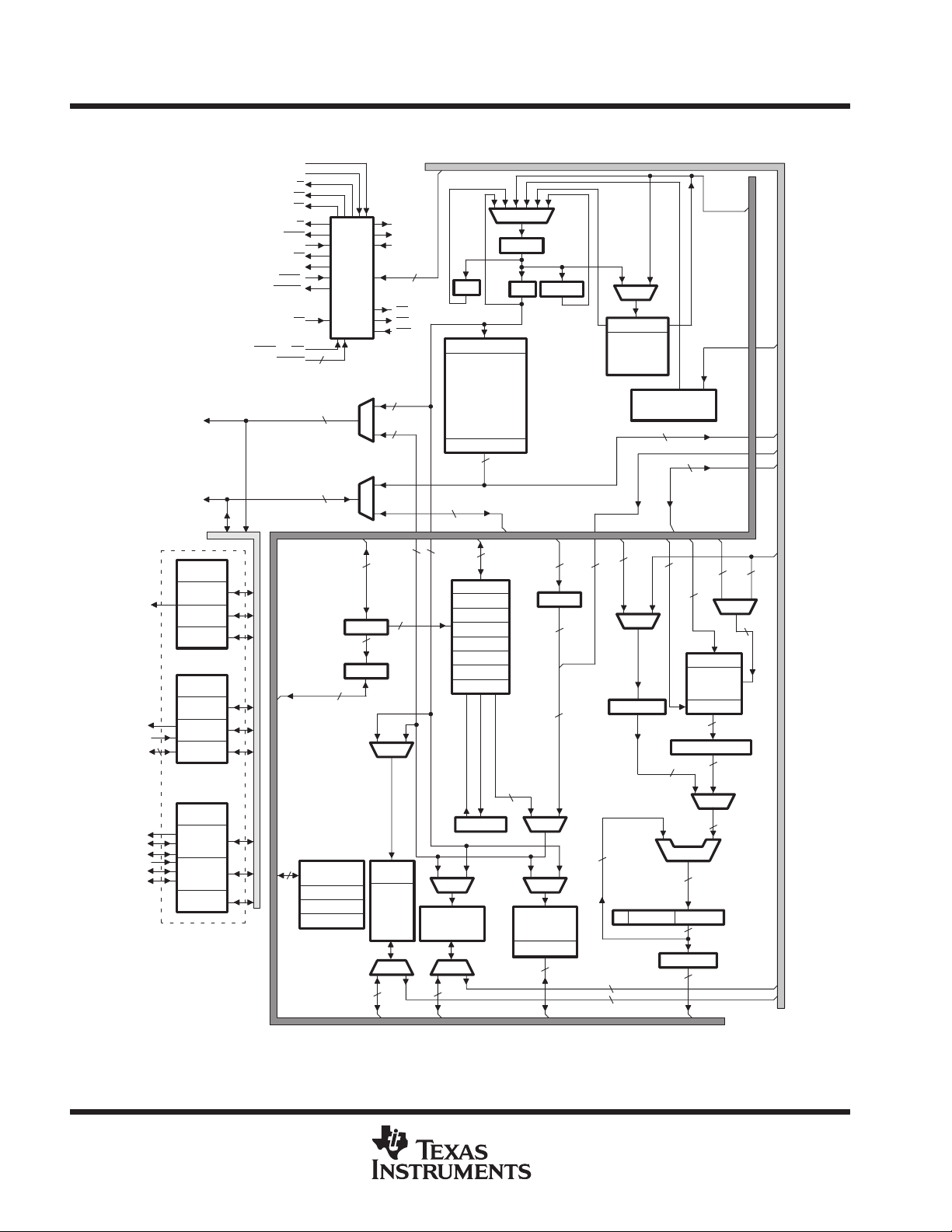
functional block diagram of the ’C2xx internal hardware
DIV1
DIV2
IS
DS
PS
R/W
STRB
READY
BR
XF
†
HOLD
†
HOLDA
RS
BOOT/MP/MC
INT[3:1]
3
A15–A0
D15–D0
Timer
TOUT
TX
RX
I/O PINS
DX
CLKX
FSX
DR
FSR
CLKR
†
Not available on all devices (see Table 2).
TCR
PRD
TIM
ASP
ADTR
IOSR
BRD
4
SSP
SSPCR
SDTR
Reserved
I/O-Mapped Registers
†
†
16
Data Bus
Memory Map
GREG (16)
16
16
3
Register
IMR (16)
IFR (16)
NOTES: A. Symbol descriptions appear in Table 3.
B. For clarity, the data and program buses are shown as single buses although they include address and data bits.
Control
MUXMUX
ARP(3)
ARB(3)
3
3
MUX
Data/Prog
SARAM
MUX
16
X1
CLKOUT1
CLKIN/X2
16
RD
WE
NMI
16
16
16
3
†
16
16
MUX
Data/Prog
DARAM
B0 (256x16)
MUX
16
PC
Instruction
ROM/FLASH
Address
16
16
AR0(16)
AR1(16)
AR2(16)
AR3(16)
AR4(16)
AR5(16)
AR6(16)
AR7(16)
ARAU(16)
†
MUX
NPAR
PAR MSTACK
DP(9)
16
MUX
MUX
Data
DARAM
B2 (32x16)
B1 (256x16)
16
Program Bus
9
9
16
MUX
Stack 8 x16
16
7
LSB
from
IR
MUX
ISCALE (0–16)
32
16
16
Program Control
(PCTRL)
16
16
16
16
PSCALE (–6,0,1,4)
CALU(32)
ACCL(16)ACCH(16)C
OSCALE (0–7)
Data Bus
TREG0(16)
Multiplier
PREG(32)
32
MUX
32
32
16
3232
32
MUX
Data Bus
1616
16
Program Bus
Program Bus
10
POST OFFICE BOX 1443 • HOUSTON, TEXAS 77251–1443
Page 11
TMS320C203, TMS320C209, TMS320LC203
DIGITAL SIGNAL PROCESSORS
SPRS025B – JUNE 1995 – REVISED AUGUST 1998
Table 3. Legend for the ’C2xx Internal Hardware Functional Block Diagram
SYMBOL NAME DESCRIPTION
ACC Accumulator
ARAU
AUX
REGS
BR Bus Register Signal
C Carry
CALU
CNF
GREG
IMR
IFR
INTM Interrupt-Mode Bit
INT# Interrupt Traps A total of 32 interrupts by way of hardware and/or software are available.
ISCALE
MPY Multiplier
MSTACK Micro Stack
MUX Multiplexer Multiplexes buses to a common input
NPAR
OSCALE
PAR Program Address
PC Program Counter
PCTRL Program Controller PCTRL decodes instruction, manages the pipeline, stores status, and decodes conditional operations.
PM
PRDB
Auxiliary Register
Arithmetic Unit
Auxiliary Registers
0–7
Central Arithmetic
Logic Unit
On-Chip RAM
Configuration
Control Bit
Global Memory
Allocation Register
Interrupt Mask
Register
Interrupt Flag
Register
Input Data-Scaling
Shifter
Next Program
Address
Output Data-Scaling
Shifter
Product Shift-Mode
Register Bits
Program-Read Data
Bus
32-bit register that stores the results and provides input for subsequent CALU operations. Also includes
shift and rotate capabilities
An unsigned, 16-bit arithmetic unit used to calculate indirect addresses using the auxiliary registers as
inputs and outputs
These 16-bit registers are used as pointers to anywhere within the data space address range. They are
operated upon by the ARAU and are selected by the auxiliary register pointer (ARP). AR0 can also be used
as an index value for AR updates of more than one and as a compare value to AR.
BR is asserted during access of the external global data memory space. READY is asserted to the device
when the global data memory is available for the bus transaction. BR
memory address space by up to 32K words.
Register carry output from CALU. C is fed back into the CALU for extended arithmetic operation. The C bit
resides in status register 1 (ST1), and can be tested in conditional instructions. C is also used in accumulator
shifts and rotates.
32-bit-wide main arithmetic logic unit for the TMS320C2xx core. The CALU executes 32-bit operations in
a single machine cycle. CALU operates on data coming from ISCALE or PSCALE with data from ACC, and
provides status results to PCTRL.
If set to 0, the reconfigurable data dual-access RAM (DARAM) blocks are mapped to data space; otherwise,
they are mapped to program space.
GREG specifies the size of the global data memory space.
IMR individually masks or enables the seven interrupts.
The 7-bit IFR indicates that the TMS320C2xx has latched an interrupt from one of the seven maskable
interrupts.
When INTM is set to 0, all unmasked interrupts are enabled. When INTM is set to 1, all maskable interrupts
are disabled.
16 to 32-bit barrel left-shifter. ISCALE shifts incoming 16-bit data 0 to16 positions left, relative to the 32-bit
output within the fetch cycle; therefore, no cycle overhead is required for input scaling operations.
16 × 16-bit multiplier to a 32-bit product. MPY executes multiplication in a single cycle. MPY operates either
signed or unsigned 2s-complement arithmetic multiply.
MSTACK provides temporary storage for the address of the next instruction to be fetched when program
address-generation logic is used to generate sequential addresses in data space.
NPAR holds the program address to be driven out on the PAB on the next cycle.
16-bit to 32-bit barrel left shifter. OSCALE shifts the 32-bit accumulator output 0 to 7 bits left for quantization
management and outputs either the 16-bit high- or low-half of the shifted 32-bit data to DWEB.
PAR holds the address currently being driven on P AB for as many cycles as it takes to complete all memory
operations scheduled for the current machine cycle.
PC increments the value from NPAR to provide sequential addresses for instruction-fetching and sequential
data-transfer operations.
These two bits identify which of the four product-shift modes (–6, 0, 1, 4) are used by PSCALE. PM resides
in ST1. See Table 7.
16-bit bus for program space read data. PRDB is driven by the memories or the logic interface.
can be used to extend the data
POST OFFICE BOX 1443 • HOUSTON, TEXAS 77251–1443
11
Page 12
TMS320C203, TMS320C209, TMS320LC203
DIGITAL SIGNAL PROCESSORS
SPRS025B – JUNE 1995 – REVISED AUGUST 1998
Table 3. Legend for the ’C2xx Internal Hardware Functional Block Diagram (Continued)
SYMBOL NAME DESCRIPTION
PREG Product Register 32-bit register holds results of 16 × 16 multiply.
0-, 1- or 4-bit left shift, or 6-bit right shift of multiplier product. The left-shift options are used to manage the
PSCALE
TREG
SSPCR
SDTR
TCR
PRD
TIM
UART
ASPCR
ADTR
IOSR
BRD Baud-Rate Divisor Used to set the baud rate of the UART
ST0
ST1
STACK Stack
Product-Scaling
Shifter
Temporary
Register
Synchronous
Serial-Port Control
Register
Synchronous
Serial-Port
Transmit and
Receive Register
Timer-Control
Register
Timer-Period
Register
Timer-Counter
Register
Universal
Asynchronous
Receive/Transmit
Asynchronous
Serial-Port Control
Register
Asynchronous
Data Register
I/O Status
Register
Status Register
additional sign bits resulting from the 2s-complement multiply. The right-shift option is used to scale down
the number to manage overflow of product accumulation in the CALU. PSCALE resides in the path from the
32-bit product shifter and from either the CALU or the Data-Write Address Bus (DWEB), and requires no
cycle overhead.
16-bit register holds one of the operands for the multiply operations. TREG holds the dynamic shift count
for the LACT, ADDT, and SUBT instructions. TREG holds the dynamic bit position for the BITT instruction.
SSPCR is the control register for selecting the serial port’s mode of operation.
SDTR is the data-transmit and data-receive register.
TCR contains the control bits that define the divide-down ratio, start/stop the timer, and reload the period.
Also contained in TCR is the current count in the prescaler. Reset initializes the timer-divide-down ratio
to 0 and starts the timer.
PRD contains the 16-bit period that is loaded into the timer counter when the counter borrows or when the
reload bit is activated. Reset initializes the PRD to 0xFFFF.
TIM contains the current 16-bit count of the timer. Reset initializes the TIM to 0xFFFF.
UART is the asynchronous serial port.
ASPCR controls the asynchronous serial-port operation.
Asynchronous data-transmit and data-receive register
IOSR detects current levels (and changes with inputs) on pins IO0–IO3 and the status of UART.
ST0 and ST1 contain the status of various conditions and modes. These registers can be stored in and
loaded from data memory , thereby allowing the status of the machine to be saved and restored.
STACK is a block of memory used for storing return addresses for subroutines and interrupt-service
routines, or for storing data. The ’C2xx stack is 16-bit wide and eight-level deep.
12
POST OFFICE BOX 1443 • HOUSTON, TEXAS 77251–1443
Page 13
TMS320C203, TMS320C209, TMS320LC203
DIGITAL SIGNAL PROCESSORS
SPRS025B – JUNE 1995 – REVISED AUGUST 1998
architectural overview
The ’C2xx advanced Harvard-type architecture maximizes the processing power by maintaining two separate
memory bus structures—program and data—for full-speed execution. This multiple bus structure allows both
data and instructions to be read simultaneously . Instructions to be read support data transfers between the two
spaces. This architecture permits coefficients that are stored in program memory to be read in RAM, thereby,
eliminating the need for a separate coefficient ROM. This, coupled with a four-deep pipeline, allows the
TMS320C2xx to execute most instructions in a single cycle.
status and control registers
Two status registers, ST0 and ST1, contain the status of various conditions and modes. These registers can
be stored in data memory and loaded from data memory , thereby, allowing the status of the machine to be saved
and restored for subroutines.
The load-status-register instruction (LST) is used to write to ST0 and ST1. The store-status-register instruction
(SST) is used to read from ST0 and ST1, except for the INTM bit, which is not affected by the LST instruction.
The individual bits of these registers can be set or cleared when using the SETC and CLRC instructions. T able 4
and T able 5 show the organization of status registers ST0 and ST1, indicating all status bits contained in each.
Several bits in the status registers are reserved and read as logic 1s. Refer to T able 6 for the status register field
definitions.
Table 4. Status and Control Register Zero
15 131211109876543210
ST0
ARP
OV OVM 1 INTM DP
Table 5. Status and Control Register One
15 131211109876543210
ST1
ARB
CNF TC SXM C 1 1 1 1 XF 1 1 PM
POST OFFICE BOX 1443 • HOUSTON, TEXAS 77251–1443
13
Page 14
TMS320C203, TMS320C209, TMS320LC203
DIGITAL SIGNAL PROCESSORS
SPRS025B – JUNE 1995 – REVISED AUGUST 1998
status and control registers (continued)
Table 6. Status Register Field Definitions
FIELD FUNCTION
ARB
ARP
C
CNF
DP
INTM
OV
OVM
PM
SXM
TC
XF
†
See Table 3 for definitions of acronyms and Table 20 for descriptions of opcode instructions.
Auxiliary register pointer buffer . Whenever the ARP is loaded, the old ARP value is copied to the ARB, except during an LST
instruction. When the ARB is loaded by way of an LST #1 instruction, the same value is also copied to the ARP.
Auxiliary register pointer. ARP selects the AR to be used in indirect addressing. When the ARP is loaded, the old ARP value
is copied to the ARB register. ARP can be modified by memory-reference instructions when using indirect addressing, and by
the LARP, MAR, and LST instructions. The ARP is also loaded with the same value as ARB when an LST #1 instruction is
executed.
Carry bit. C is set to 1 if the result of an addition generates a carry; it is reset to 0 if the result of a subtraction generates a borrow.
Otherwise, C is reset after an addition or set after a subtraction, except when the instruction is ADD or SUB with a 16-bit shift.
In these cases, the ADD can only set and the SUB can only reset the carry bit, but cannot affect it otherwise. The single-bit
shift and rotate instructions also affect C, as well as the SETC, CLRC, and LST #1 instructions. Branch instructions have been
provided to branch on the status of C. C is set to 1 on a reset.
On-chip RAM configuration control bit. If CNF is set to 0, the reconfigurable data DARAM blocks are mapped to data space;
otherwise, they are mapped to program space. The CNF can be modified by the SETC CNF, CLRC CNF, and LST #1
instructions. RS
Data-memory page pointer. The 9-bit DP register is concatenated with the seven LSBs of an instruction word to form a direct
memory address of 16 bits. DP can be modified by the LST and LDP instructions.
Interrupt-mode bit. When INTM is set to 0, all unmasked interrupts are enabled. When INTM is set to 1, all maskable interrupts
are disabled. INTM is set and reset by the SETC INTM and CLRC INTM instructions. RS
no effect on the unmaskable RS
by reset. It is also set to 1 when a maskable interrupt trap is taken.
Overflow-flag bit. As a latched overflow signal, OV is set to 1 when overflow occurs in the ALU. Once an overflow occurs, the
OV remains set until a reset, BCND/D on OV/NOV, or LST instruction clears OV.
Overflow-mode bit. When OVM is set to 0, overflowed results overflow normally in the accumulator. When OVM is set to 1, the
accumulator is set to either its most positive or negative value upon encountering an overflow. The SETC and CLRC
instructions set and reset this bit, respectively. LST can also be used to modify the OVM.
Product-shift-mode bits. If these two bits are 00, the multiplier’s 32-bit product is loaded into the ALU with no shift. If PM = 01,
the product register (PREG) output is left-shifted one place and loaded into the ALU, with the LSB zero-filled. If PM = 10, the
PREG output is left-shifted by 4 bits and loaded into the ALU, with the LSBs zero-filled. PM = 11 produces a right shift of 6 bits,
sign-extended. Note that the PREG contents remain unchanged. The shift takes place when transferring the contents of the
PREG to the ALU. PM is loaded by the SPM and LST #1 instructions. PM is cleared by RS
Sign-extension mode bit. SXM = 1 produces sign-extension on data as it is passed into the accumulator through the scaling
shifter. SXM = 0 suppresses sign-extension. SXM does not af fect the definitions of certain instructions; for example, the ADDS
instruction suppresses sign-extension regardless of SXM. SXM is set by the SETC SXM instruction, reset by the CLRC SXM
instruction, and can be loaded by the LST #1 instruction. SXM is set to 1 by reset.
T est/control flag bit. TC is affected by the BIT, BITT , CMPR, LST #1, and NORM instructions. TC is set to a 1 if a bit tested by
BIT or BITT is a 1, if a compare condition tested by CMPR exists between AR (ARP) and AR0, or if the exclusive-OR function
of the two MSBs of the accumulator is true when tested by a NORM instruction. The conditional branch, call, and return
instructions can execute based on the condition of TC.
XF pin status bit. XF indicates the state of the XF pin, a general-purpose output pin. XF is set by the SETC XF and reset by
the CLRC XF instructions. XF is set to 1 by reset.
sets the CNF to 0.
and NMI interrupts. Note that INTM is unaffected by the LST instruction. This bit is set to 1
†
and IACK also set INTM. INTM has
.
central processing unit
The TMS320C2xx central processing unit (CPU) contains a 16-bit scaling shifter, a 16 × 16-bit parallel multiplier ,
a 32-bit central arithmetic logic unit (CALU), a 32-bit accumulator, and additional shifters at the outputs of both
the accumulator and the multiplier. This section describes the CPU components and their functions. The
functional block diagram shows the components of the CPU.
14
POST OFFICE BOX 1443 • HOUSTON, TEXAS 77251–1443
Page 15

TMS320C203, TMS320C209, TMS320LC203
DIGITAL SIGNAL PROCESSORS
SPRS025B – JUNE 1995 – REVISED AUGUST 1998
input scaling shifter
The TMS320C2xx provides a scaling shifter with a 16-bit input connected to the data bus and a 32-bit output
connected to the CALU. This shifter operates as part of the path of data coming from program or data space
to the CALU and requires no cycle overhead. It is used to align the 16-bit data coming from memory to the 32-bit
CALU. This is necessary for scaling arithmetic as well as aligning masks for logical operations.
The scaling shifter produces a left shift of 0 to 16 on the input data. The LSBs of the output are filled with zeros;
the MSBs can be either filled with zeros or sign-extended, depending upon the value of the SXM bit
(sign-extension mode) of status register ST1. The shift count is specified by a constant embedded in the
instruction word or by a value in the temporary register (TREG). The shift count in the instruction allows for
specific scaling or alignment operations specific to that point in the code. The TREG base shift allows the scaling
factor to be adaptable to the system’s performance.
multiplier
The TMS320C2xx uses a 16 × 16-bit hardware multiplier that is capable of computing a signed or an unsigned
32-bit product in a single machine cycle. All multiply instructions, except the MPYU (multiply unsigned)
instruction, perform a signed multiply operation. That is, two numbers being multiplied are treated as
2s-complement numbers, and the result is a 32-bit 2s-complement number. There are two registers associated
with the multiplier: a 16-bit temporary register (TREG) that holds one of the operands for the multiplier, and a
32-bit product register (PREG) that holds the product.
Four product-shift modes (PM) are available at the PREG’s output (PSCALE). These shift modes are useful for
performing multiply/accumulate operations, performing fractional arithmetic, or justifying fractional products.
The PM field of status register ST1 specifies the PM shift mode, as shown in Table 7.
Table 7. PSCALE Product-Shift Modes
PM SHIFT DESCRIPTION
00 no shift Product feed to CALU or data bus with no shift
01 left 1 Removes the extra sign bit generated in a 2s-complement multiply to produce a Q31 product
10 left 4 Removes the extra four sign bits generated in a 16 × 13 2s-complement multiply to a produce a Q31
11 right 6 Scales the product to allow up to 128 product accumulations without the possibility of accumulator overflow
product when using the multiply by a 13-bit constant
The product can be shifted one bit to compensate for the extra sign bit gained in multiplying two 16-bit
2s-complement numbers (MPY). A 4-bit shift is used in conjunction with the MPY instruction with a short
immediate value (13 bits or less) to eliminate the four extra sign bits gained in multiplying a 16-bit number by
a 13-bit number. Finally, the output of PREG can be right-shifted 6 bits to enable the execution of up to
128 consecutive multiply/accumulates without the possibility of overflow.
The L T (load TREG) instruction normally loads TREG to provide one operand (from the data bus), and the MPY
(multiply) instruction provides the section operand (also from the data bus). A multiplication can also be
performed with a 13-bit immediate operand when using the MPY instruction. A product is then obtained every
two cycles. When the code is executing multiple multiplies and product sums, the CPU supports the pipelining
of the TREG load operations with CALU operations using the previous product. These pipeline operations that
run in parallel with loading the TREG include: load ACC with PREG (L TP); add PREG to ACC (L TA); add PREG
to ACC and shift TREG input data (DMOV) to next address in data memory (L TD); and subtract PREG from ACC
(L TS).
POST OFFICE BOX 1443 • HOUSTON, TEXAS 77251–1443
15
Page 16

TMS320C203, TMS320C209, TMS320LC203
DIGITAL SIGNAL PROCESSORS
SPRS025B – JUNE 1995 – REVISED AUGUST 1998
multiplier (continued)
Two multiply/accumulate instructions (MAC and MACD) fully utilize the computational bandwidth of the
multiplier, allowing both operands to be processed simultaneously. The data for these operations can be
transferred to the multiplier each cycle by way of the program and data buses. This facilitates single-cycle
multiply/accumulates when used with the repeat (RPT) instruction. In these instructions, the coefficient
addresses are generated by program address generation (PAGEN), while the data addresses are generated
by data-address generation (DAGEN). This allows the repeated instruction to sequentially access the values
from the coefficient table and step through the data in any of the indirect addressing modes.
The MACD instruction, when repeated, supports filter constructs (weighted running averages) so that as the
sum-of-products is executed, the sample data is shifted in memory to make room for the next sample and to
throw away the oldest sample.
The MPYU instruction performs an unsigned multiplication, which greatly facilitates extended-precision
arithmetic operations. The unsigned contents of TREG are multiplied by the unsigned contents of the addressed
data memory location, with the result placed in PREG. This allows the operands of greater than 16 bits to be
broken down into 16-bit words and processed separately to generate products of greater than 32 bits. The
SQRA (square/add) and SQRS (square/subtract) instructions pass the same value to both inputs of the
multiplier for squaring a data-memory value.
After the multiplication of two 16-bit numbers, the 32-bit product is loaded into the 32-bit product register
(PREG). The product from PREG can be transferred to the CALU or to data memory by way of the SPH (store
product-high register) and the SPL (store product-low register) instructions. Note: the transfer of PREG to either
the CALU or data memory passes through the product-scaling shifter (PSCALE) and is therefore affected by
the product-shift mode defined by PM bits in the ST1 register. This is important when saving PREG in an
interrupt-service-routine-context save as the PSCALE shift effects cannot be modeled in the restore operation.
PREG can be cleared by executing the MPY #0 instruction. The product register can be restored by loading the
saved low half into TREG and executing the MPY #1 instruction. The high half is then loaded using the LPH
instruction.
central arithmetic logic unit
The TMS320C2xx central arithmetic logic unit (CALU) implements a wide range of arithmetic and logical
functions, the majority of which execute in a single clock cycle. This arithmetic logic unit (ALU) is referred to as
“central” to differentiate it from a second ALU used for indirect-address-generation (called the ARAU). Once an
operation is performed in the CALU, the result is transferred to the accumulator (ACC), where additional
operations, such as shifting, can occur. Data that is input to the CALU can be scaled by the input data-scaling
shifter (ISCALE) when coming from one of the data buses (DRDB or PRDB) or scaled by PSCALE when coming
from the multiplier.
The CALU is a general-purpose arithmetic/logic unit that operates on 16-bit words taken from data memory or
derived from immediate instructions. In addition to the usual arithmetic instructions, the CALU can perform
Boolean operations, facilitating the bit manipulation ability required for a high-speed controller. One input to the
CALU is always provided from the accumulator, and the other input can be provided from the product register
(PREG) of the multiplier or the output of the scaling shifter (that has been read from data memory or from the
ACC). After the CALU has performed the arithmetic or logical operation, the result is stored in the accumulator.
The TMS320C2xx supports floating-point operations for applications requiring a large dynamic range. The
NORM (normalization) instruction is used to normalize fixed-point numbers contained in the accumulator by
performing left shifts. The four bits of the TREG define a variable shift through the scaling shifter for the
LACT/ADDT/SUBT (load/add to/subtract from accumulator with shift specified by TREG) instructions. These
instructions are useful in floating-point arithmetic where a number needs to be denormalized—that is,
floating-point to fixed-point conversion. They are also useful in the execution of an automatic gain control (AGC)
going into a filter. The BITT (bit-test) instruction provides testing of a single bit of a word in data memory based
on the value contained in the four LSBs of TREG.
16
POST OFFICE BOX 1443 • HOUSTON, TEXAS 77251–1443
Page 17

TMS320C203, TMS320C209, TMS320LC203
DIGITAL SIGNAL PROCESSORS
SPRS025B – JUNE 1995 – REVISED AUGUST 1998
central arithmetic logic unit (continued)
The CALU overflow-saturation mode can be enabled/disabled by setting/resetting the overflow mode (OVM)
bit of ST0. When the CALU is in the overflow-saturation mode and an overflow occurs, the overflow flag is set
and the accumulator is loaded with either the most positive or the most negative value representable in the
accumulator, depending upon the direction of the overflow. The value of the accumulator upon saturation is
07FFFFFFFh (positive) or 080000000h (negative). If the OVM status register bit is reset and an overflow occurs,
the overflowed results are loaded into the accumulator with modification. (Note that logical operations cannot
result in overflow.)
The CALU can execute a variety of branch instructions that depend on the status of the CALU and the
accumulator. These instructions can be executed conditionally, based on any meaningful combination of these
status bits. For overflow management, these conditions include the OV (branch on overflow) and EQ (branch
on accumulator equal to zero). In addition, the BACC (branch to address in accumulator) instruction provides
the ability to branch to an address specified by the accumulator (computed goto). Bit-test instructions (BIT and
BITT), which do not affect the accumulator, allow the testing of a specified bit of a word in data memory.
The CALU also has a carry bit that is set or reset depending on various operations within the device. The carry
bit allows more efficient computation of extended-precision products and additions or subtractions. It is also
useful in overflow management. The carry bit is affected by most arithmetic instructions as well as the single-bit
shift and rotate instructions. It is not affected by accumulator loads, logical operations, or other such
non-arithmetic or control instructions.
D
Additions to and subtractions from the accumulator:
C = 0: When the result of a subtraction generates a borrow.
When the result of an addition does not generate a carry . (Exception: When the ADD instruction is
used with a shift of 16 and no carry is generated, the ADD instruction has no effect on C.)
C = 1: When the result of an addition generates a carry.
When the result of a subtraction does not generate a borrow. (Exception: When the SUB instruction
is used with a shift of 16 and no borrow is generated, the SUB instruction has no effect on C.)
D
Single-bit shifts and rotations of the accumulator value. During a left shift or rotation, the most significant
bit of the accumulator is passed to C; during a right shift or rotation, the least significant bit is passed to C.
Note: the carry bit is set to “1” on a hardware reset.
The ADDC (add to accumulator with carry) and SUBB (subtract from accumulator with borrow) instructions
provide the use of the previous value of carry in their addition/subtraction operation.
The one exception to the operation of the carry bit is in the use of ADD with a shift count of 16 (add to high
accumulator) and SUB with a shift count of 16 (subtract from high accumulator) instructions. This case of the
ADD instruction can set the carry bit only if a carry is generated, and this case of the SUB instruction can reset
the carry bit only if a borrow is generated; otherwise, neither instruction affects it.
Two conditional operands, C and NC, are provided for branching, calling, returning, and conditionally executing
based upon the status of the carry bit. The SETC, CLRC, and LST #1 instructions also can be used to load the
carry bit. The carry bit is set to one on a hardware reset.
accumulator
The 32-bit accumulator is the registered output of the CALU. It can be split into two 16-bit segments for storage
in data memory. Shifters at the output of the accumulator provide a left shift of 0 to 7 places. This shift is
performed while the data is being transferred to the data bus for storage. The contents of the accumulator
remain unchanged. When the post-scaling shifter is used on the high word of the accumulator (bits 16–31), the
MSBs are lost and the LSBs are filled with bits shifted in from the low word (bits 0–15). When the post-scaling
shifter is used on the low word, the LSBs are zero-filled.
POST OFFICE BOX 1443 • HOUSTON, TEXAS 77251–1443
17
Page 18

TMS320C203, TMS320C209, TMS320LC203
DIGITAL SIGNAL PROCESSORS
SPRS025B – JUNE 1995 – REVISED AUGUST 1998
accumulator (continued)
The SFL and SFR (in-place one-bit shift to the left/right) instructions and the ROL and ROR (rotate to the
left/right) instructions implement shifting or rotating of the accumulator contents through the carry bit. The SXM
status register bit affects the definition of the SFR (shift accumulator right) instruction. When SXM = 1, SFR
performs an arithmetic right shift, maintaining the sign of the accumulator data. When SXM = 0, SFR performs
a logical shift, shifting out the LSBs and shifting in a zero for the MSB. The SFL (shift accumulator left) instruction
is not affected by the SXM bit and behaves the same in both cases, shifting out the MSB and shifting in a zero.
RPT (repeat) instructions can be used with the shift and rotate instructions for multiple-bit shifts.
auxiliary registers and auxiliary-register arithmetic unit (ARAU)
The ’C2xx provides a register file containing eight auxiliary registers (AR0–AR7). The auxiliary registers are
used for indirect addressing of the data memory or for temporary data storage. Indirect auxiliary-register
addressing allows placement of the data memory address of an instruction operand into one of the auxiliary
registers. These registers are referenced with a 3-bit auxiliary register pointer (ARP) that is loaded with a value
from 0 through 7, designated AR0 through AR7, respectively . The auxiliary registers and the ARP can be loaded
from data memory, the ACC, the product register, or by an immediate operand defined in the instruction. The
contents of these registers can also be stored in data memory or used as inputs to the CALU.
The auxiliary register file is connected to the ARAU. The ARAU can autoindex the current auxiliary register while
the data memory location is being addressed. Indexing either by ±1 or by the contents of AR0 can be performed.
As a result, accessing tables of information does not require the CALU for address manipulation; therefore, the
CALU is free for other operations in parallel.
memory
The ’C2xx implements three separate address spaces for program memory , data memory, and I/O. Each space
accommodates a total of 64K 16-bit words. Within the 64K words of data space, the 256 to 32K words at the
top of the address range can be defined to be external global memory in increments of powers of two, as
specified by the contents of the global memory allocation register. Access to global memory is arbitrated using
the global memory bus request (BR
On the ’C2xx, the first 96 (0–5Fh) data memory locations are allocated for memory-mapped registers or are
reserved. This memory-mapped register space contains various control and status registers including those for
the CPU.
When using on-chip RAM, or high-speed external memory , the ’C2xx runs at full speed with no wait states. The
ability of the DARAM to allow two accesses to be performed in one cycle, coupled with the parallel nature of
the ’C2xx architecture, enables the device to perform three concurrent memory accesses in any given machine
cycle. Externally , the READY line can be used to interface the ’C2xx to slower, less expensive external memory .
Downloading programs from slow off-chip memory to on-chip RAM can speed processing while cutting system
costs.
The ’C2xx DARAM allows writes to and reads from the RAM in the same cycle without the address restrictions
of the SARAM. The DARAM is configured in three blocks: block 0 (B0), block 1 (B1), and block 2 (B2).
Block 1 consists of 256 words in data memory and block 2 consists of 32 words in data memory. Block 0 is a
256-word block that can be configured as data or program memory . The SETC CNF (configure B0 as program
memory) and CLRC CNF (configure B0 as data memory) instructions allow dynamic configuration of the
memory maps through software. When using Block 0 as program memory , instructions can be downloaded from
external program memory into on-chip RAM and then executed.
) signal.
18
POST OFFICE BOX 1443 • HOUSTON, TEXAS 77251–1443
Page 19
TMS320C203, TMS320C209, TMS320LC203
DIGITAL SIGNAL PROCESSORS
SPRS025B – JUNE 1995 – REVISED AUGUST 1998
memory (continued)
TMS320C209 (only)
The mask-programmable ROM is located in program memory space. Customers can arrange to have this ROM
programmed with contents unique to any particular application. The ROM is enabled or disabled by the state
of the MP/MC
when enabled. When disabled, these addresses are located in the device’s external program memory space.
The ’C209 devices provide two types of RAM: single-access RAM (SARAM) and dual-access RAM (DARAM).
The SARAM requires a full machine cycle to perform a read or a write. However, this is not one large RAM block
in which only one access per cycle is allowed. It is made up of 2K-word size-independent RAM blocks and each
one allows one CPU access per cycle. The CPU can read or write one block while accessing another block at
the same time. The ’C209 processor supports multiple accesses to its SARAM in one cycle as long as they go
to different RAM blocks. With an understanding of this structure, code and data can be appropriately arranged
to improve code performance.
The TMS320C203 includes three registers mapped to internal data space and peripheral registers mapped to
internal I/O space. Figure 1, T able 6, and T able 7 describe these registers and show their respective addresses.
They also show the effects of the memory-control pin BOOT
respective memory spaces to on-chip or off-chip memory.
control input upon resetting the device. The ROM occupies the lowest block of program memory
and control bit CNF on the mapping of the
Both of the TMS320C2xx devices include 544 × 16 words of dual-access RAM. The ’C209 device includes
4K × 16 words of single-access RAM and 4K × 16 words of ROM integrated with CPU. Figure 1, Table 6, and
Table 7 show the mapping of the memory blocks and the appropriate control bits and pins for the ’C203. For
the ’C209 devices, Figure 2, Table 8, and Table 9, show the effects of the memory-control pins MP/MC
and
RAMEN, and control bit CNF on the mapping of the respective memory spaces to on-chip or off-chip memory.
Program
Hex
0000
003F
0040
FDFF
FE00
FEFF
FF00
FFFF
Interrupts
(External)
External
Reserved (CNF = 1)
External (CNF = 0)
On-Chip DARAM
B0 (CNF = 1)
External (CNF = 0)
BOOT
Microprocessor Mode
= 1
Hex
0000
003F
0040
FDFF
FE00
FEFF
FF00
FFFF
Program
Interrupts
(External)
External
Reserved (CNF = 1)
External (CNF = 0)
On-Chip DARAM
B0 (CNF = 1)
External (CNF = 0)
= 0
BOOT
Microprocessor Mode
(Boot-Loader Enabled)
Hex
0000
005F
0060
007F
0080
01FF
0200
02FF
0300
03FF
0400
Memory-Mapped
Registers and
On-Chip DARAM
Reserved (CNF = 1)
Data
Reserved
On-Chip
DARAM B2
Reserved
B0 (CNF = 0)
On-Chip
DARAM B1
Reserved
07FF
FFFF
Figure 1. TMS320C203/LC203 Memory Map
POST OFFICE BOX 1443 • HOUSTON, TEXAS 77251–1443
0800
External
19
Page 20
TMS320C203, TMS320C209, TMS320LC203
BOOT
CNF
DIGITAL SIGNAL PROCESSORS
SPRS025B – JUNE 1995 – REVISED AUGUST 1998
memory (continued)
Table 8. TMS320C203/LC203 Memory Map Configurations
ON-CHIP MEMORY OFF-CHIP MEMORY
PROGRAM DATA I/O PROGRAM DATA I/O
0 0 — 0–7FF FF00–FFFF 0000–FFFF 800–FFFF 0–FEFF
0 1 FE00–FFFF
1 0 — 0–7FF FF00–FFFF 0000–FFFF 800–FFFF 0–FEFF
1 1 FE00–FFFF 0–7FF FF00–FFFF 0000–FDFF 800–FFFF 0–FEFF
†
Internal I/O locations 0FFE0h–0FFFFh are dedicated to the timer, serial-port control, wait-state generator registers, and reserved space.
‡
FF00–FF0F are reserved for test purposes and should not be used.
§
When BOOT
= 0, the on-chip boot-loader at 0xFF00h is enabled. During boot time, memory address FE00–FFFF is reserved.
§
0–7FF FF00–FFFF 0000–FDFF 800–FFFF 0–FEFF
†
Table 9. TMS320C203/LC203 On-Chip Memory Map
DESCRIPTION OF MEMORY BLOCK
On-chip bootloader FF00–FFFFh low
256 × 16 word dual-access RAM (DARAM) (B0)
256 × 16 word DARAM (B0)
256 × 16 word DARAM (B1)
32 × 16 word DARAM (B2) 0x60–0x7Fh
¶
Each of these address pairs point to the same block of memory.
DATA
ADDRESS
0x100–0x1FFh
0x200–0x2FFh
0x300–0x3FFh
0x400–0x4FFh
¶
¶
¶
¶
PROG
ADDRESS
0xFE00–0xFEFF
0xFF00–0xFFFF
BOOT
¶
¶
CNF
BIT
0
1
‡
bootloader
The bootloader is used to transfer user code from an external global data memory source to program memory
automatically at reset. This function is useful for initializing external RAM using external ROM. If the BOOT
is sampled low during a hardware reset, a reset vector is internally generated forcing a branch to the on-chip
boot ROM at address location FF00h. The code is read in parallel from an 8-bit-wide EPROM and transferred
to the 16-bit-wide destination. The maximum size for the EPROM, is 32K words × 8-bits.
transferred define the destination address and program length. After the bootload is complete, the ’C203
removes the boot ROM from the memory map. For a detailed description of bootloader functionality, refer to
the
TMS320C2xx User’s Guide
#
The address range 8000h – FEFFh equals 32 512 words.
(literature number SPRU127).
#
The first four bytes
pin
20
POST OFFICE BOX 1443 • HOUSTON, TEXAS 77251–1443
Page 21
memory (continued)
TMS320C203, TMS320C209, TMS320LC203
DIGITAL SIGNAL PROCESSORS
SPRS025B – JUNE 1995 – REVISED AUGUST 1998
Program
Hex
0000
003F
0040
0FFF
1000
1FFF
2000
FDFF
FE00
FEFF
FF00
FFFF
Interrupts
(External)
External
On-Chip SARAM
(RAMEN = 1)
External
(RAMEN = 0)
External
Reserved (CNF = 1)
External (CNF = 0)
On-Chip DARAM
B0 (CNF = 1)
External (CNF = 0)
MP/MC = 1
Microprocessor Mode
Hex
0000
003F
0040
0FFF
1000
1FFF
2000
FDFF
FE00
FEFF
FF00
FFFF
Interrupts
(On-Chip)
On-Chip ROM
On-Chip SARAM
(RAMEN = 1)
(RAMEN = 0)
Reserved (CNF = 1)
External (CNF = 0)
On-Chip DARAM
B0 (CNF = 1)
External (CNF = 0)
MP/MC = 0
Microcomputer Mode
Program
External
External
Hex
0000
005F
0060
007F
0080
01FF
0200
02FF
0300
03FF
0400
07FF
0800
0FFF
1000
1FFF
2000
FFFF
Memory-Mapped
Registers and
On-Chip DARAM
Reserved (CNF = 1)
On-Chip SARAM
Data
Reserved
On-Chip
DARAM B2
Reserved
B0 (CNF = 0)
On-Chip
DARAM B1
Reserved
External
(RAMEN = 0)
Reserved
(RAMEN = 1)
(RAMEN = 1)
External
(RAMEN = 0)
External
Figure 2. TMS320C209 Memory Map
POST OFFICE BOX 1443 • HOUSTON, TEXAS 77251–1443
21
Page 22
TMS320C203, TMS320C209, TMS320LC203
MP/MC
RAMEN
CNF
DIGITAL SIGNAL PROCESSORS
SPRS025B – JUNE 1995 – REVISED AUGUST 1998
memory (continued)
Table 10. TMS320C209 Memory Map Configurations
ON-CHIP OFF-CHIP
PROGRAM DATA I/O PROGRAM DATA I/O
0 1 0 0–1FFF 0–1FFF FFF0–FFFF 2000–FFFF 2000–FFFF 0–FFEF
0 1 1
0 0 0 0–0FFF 0–07FF FFF0–FFFF 1000–FFFF 0800–FFFF 0–FFEF
0 0 1
1 1 0 1000–1FFF 0–1FFF FFF0–FFFF
1 1 1
1 0 0 0–07FF FFF0–FFFF 0–FFFF 0800–FFFF 0–FFEF
1 0 1 FE00–FFFF 0–07FF FFF0–FFFF 0–FDFF 0800–FFFF 0–FFEF
†
Internal I/O locations 0FFF0h–0FFFFh are dedicated to the timer, wait-state generator registers, and reserved space.
‡
FF00–FF0F are reserved for test purposes and should not be used.
0–1FFF
FE00–FFFF
0–0FFF
FE00–FFFF
1000–1FFF
FE00–FFFF
0–1FFF FFF0–FFFF 2000–FDFF 2000–FFFF 0–FFEF
0–07FF FFF0–FFFF 1000–FDFF 0800–FFFF 0–FFEF
0–1FFF FFF0–FFFF
†
0–FFF
2000–FFFF
0–FFF
2000–FDFF
‡
2000–FFFF 0–FFEF
2000–FFFF 0–FFEF
Table 11. TMS320C209 On-Chip Memory Map
DESCRIPTION OF MEMORY BLOCK
4K × 16 words of factory-masked ROM 0000–0FFFh low
256 × 16 words DARAM (B0)
256 × 16 words DARAM (B0)
256 × 16 words DARAM (B1)
32 × 16 words DARAM (B2) 0x60–0x7Fh
4096 × 16 words single access RAM (SARAM) 0x1000–0x1FFFh 0x1000–0x1FFFh high
§
Both of the addresses in each of these address pairs point to the same block of memory.
DATA
ADDRESS
0x100–0x1FFh
0x200–0x2FFh
0x300–0x3FFh
0x400–0x4FFh
§
§
§
§
PROG
ADDRESS
0xFE00–0xFEFF
0xFF00–0xFFFF
MP/MC
§
§
CNF
BIT
0
1
RAMEN
22
POST OFFICE BOX 1443 • HOUSTON, TEXAS 77251–1443
Page 23
TMS320C203, TMS320C209, TMS320LC203
DIGITAL SIGNAL PROCESSORS
SPRS025B – JUNE 1995 – REVISED AUGUST 1998
memory (continued)
Table 12 shows the names, addresses, and functional descriptions of the TMS320C203 memory and I/O
internally mapped registers.
Table 12. TMS320C203 Memory and I/O Internally Mapped Registers
NAME ADDRESS DESCRIPTION
Interrupt-mask register. IMR individually masks or enables the seven interrupts. Bit 0 shares the external interrupt
pins INT1
IMR DS@0004
GREG DS@0005
IFR DS@0006
CLK IS@FFE8
ICR IS@FFEC
SDTR IS@FFF0 Synchronous serial-port (SSP) transmit and receive register
SSPCR IS@FFF1 Synchronous serial-port control register
ADTR IS@FFF4 Asynchronous serial-port (ASP) transmit and receive register
ASPCR IS@FFF5 Asynchronous serial-port control register. ASPCR controls the asynchronous serial port operation.
IOSR IS@FFF6 I/O status register. IOSR detects current levels (and changes with inputs) on pins IO0–IO3 and status of UAR T.
BRD IS@FFF7 Baud-rate divisor . Used to set baud rate of UART
TCR IS@FFF8
PRD IS@FFF9
TIM IS@FFFA Timer-counter register . TIM contains the current 16-bit count of the timer. Reset initializes the TIM to 0xFFFF.
WSGR IS@FFFC
†
During on-chip I/O access, IS
XINT
interrupts for the asynchronous serial port, ASP. Bit 6 is reserved for monitor mode emulation operations and
should always be set to 0 except in conjunction with emulation monitor operations. Bits 7–15 are not used in the
TMS320C203. IMR is set to 0 at reset.
Global memory allocation register. GREG specifies the size of the global memory space. GREG is set to 0 at
reset.
Interrupt-flag register. IFR indicates that the TMS320C203 has latched an interrupt from one of the seven
maskable interrupts. Bit 0 shares the external interrupt INT1
the timer interrupt, TINT
Bit 5, TXRXINT
reserved for monitor mode emulation operations and should always be set to 0 except in conjunction with
emulation monitor operations. Writing a 1 to the respective interrupt bit clears an active flag and the respective
pending interrupt. Writing a 1 to an inactive flag has no effect. Bits 7–15 are not used in the TMS320C203. IMR
is set to 0 at reset.
CLKOUT1 on or off. At reset, CLKOUT1 is configured as a zero for the pin to be active (on). If CLKOUT1 is a 1,
the CLKOUT1 pin is turned off.
Interrupt-control register . ICR is used to determine which interrupt is active since INT1 and HOLD share an interrupt vector as do INT1
is for pending interrupts (similar to IFR). At reset, all bits are zeroed, enabling HOLD mode. The MODE bit is used
by the hold-generating circuit to determine if a HOLD
Timer-control register. TCR contains the control bits that define the divide-down ratio, start/stop the timer, and
reload the period. Also contained in TCR is the current count in the prescaler. Reset initializes the timer
divide-down ratio to 0 and starts the timer.
Timer-period register. PRD contains the 16-bit period that is loaded into the timer counter when the counter
borrows or when the reload bit is activated. Reset initializes the PRD to 0xFFFF.
Wait-state-generator register . WSGR contains 12 control bits to enable 0, . . . ,7 wait states to program, data, and
I/O space. Reset initializes the WSGR to 0x0FFFh.
, RD, and WR are not visible at the pins (’C203 only).
and HOLD. INT2 and INT3 share bit 1. Bit 2 ties to the timer interrupt, TINT. Bits 3 and 4, RINT and
, respectively, are for the synchronous serial port, SSP. Bit 5, TXRXINT, shares the transmit and receive
and HOLD. INT2 and INT3 share bit 1. Bit 2 ties to
. Bits 3 and 4, RINT and XINT, respectively, are for the synchronous serial port, SSP.
, shares the transmit- and receive-interrupts for the asynchronous serial port, ASP. Bit 6 is
and INT3. A portion of this register is for mask/unmask (similar to IMR) and another portion
or INT1 is active.
†
POST OFFICE BOX 1443 • HOUSTON, TEXAS 77251–1443
23
Page 24
TMS320C203, TMS320C209, TMS320LC203
DIGITAL SIGNAL PROCESSORS
SPRS025B – JUNE 1995 – REVISED AUGUST 1998
memory (continued)
Table 13 shows the names, addresses, and functional descriptions of the TMS320C209 memory-mapped
registers.
Table 13. TMS320C209 Memory-Mapped Registers
NAME ADDRESS DESCRIPTION
Interrupt-mask register. IMR individually masks or enables the seven interrupts. The lower three bits align to the
three external interrupt pins (bit 0 ties to INT1
IMR DS@0004
GREG DS@0005
IFR DS@0006
TCR IS@FFFC
PRD IS@FFFD
TIM IS@FFFE Timer-counter register. TIM contains the current 16-bit count of the timer. Reset initializes the TIM to 0xFFFF.
WSGR IS@FFFF
Bits 4 and 5 are not used in the TMS320C209. Bit 6 is reserved for monitor mode emulation operations and should
always be set to 0 except in conjunction with emulation monitor operations. Bits 7–15 are not used in the
TMS320C209. IMR is set to 0 at reset.
Global memory allocation register. GREG specifies the size of the global memory space. GREG is set to 0 at
reset.
Interrupt-flag register . IFR indicates that the ’C2xx core has latched an interrupt pulse from one of the maskable
interrupts. The lower three bits align to the three external interrupt pins (bit 0 ties to INT1
bit 2 to INT3
should always be set to 0 except in conjunction with emulation monitor operations. A 1 indicates an active
interrupt in the respective interrupt location. Writing a 1 to the respective interrupt bit clears an active flag and
the respective pending interrupt. Writing a 1 to an inactive flag has no affect. IFR is set to 0 at reset.
Timer-control register. TCR contains the control bits that define the divide-down ratio, start/stop the timer, and
reload the period. Also contained in TCR is the current count in the prescaler. Reset initializes the timer
divide-down ratio to 0 and starts the timer.
Timer-period register. PRD contains the 16-bit period that is loaded into the timer counter when the counter
borrows or when the reload bit is activated. Reset initializes the PRD to 0xFFFF.
Wait-state generator register . WSGR contains the three control bits to enable a single wait state each of program,
data, and I/O space as well as the address-visibility-enable bit. Reset initializes WSGR to 0xF.
). Bit 3 ties to the timer interrupt. Bits 4–15 are reserved for monitor mode emulation operations and
, bit 1 to INT2, and bit 2 to INT3). Bit 3 ties to the timer interrupt.
, bit 1 to INT2, and
external interface
The TMS320C2xx can address up to 64K × 16 words of memory or registers in each of the program, data, and
I/O spaces. On-chip memory, when enabled, removes some of this off-chip range. In data space, the high
32K words can be dynamically mapped either locally or globally using the GREG register as described in the
TMS320C2xx User’s Guide
BR
low (with timing similar to the address bus) (see Table 11).
The CPU of the TMS320C2xx schedules a program-fetch, data-read, and data-write on the same machine
cycle. This is because from on-chip memory, the CPU can execute all three of these operations in the same
cycle. However, the external interface multiplexes the internal buses to one address bus and one data bus. The
external interface sequences these operations to complete first the data-write, then the data-read, and finally
the program-read.
The ’C2xx supports a wide range of system-interfacing requirements. Program, data, and I/O address spaces
provide interface to memory and I/O, thereby maximizing system throughput. The full 16-bit address and data
bus, along with the PS
three spaces.
I/O design is simplified by having I/O treated the same way as memory. I/O devices are mapped into the I/O
address space using the processor’s external address and data buses in the same manner as memory-mapped
devices.
(literature number SPRU127). A data-memory access mapped as global asserts
, DS, and IS space-select signals, allow addressing of 64K 16-bit words in each of the
24
POST OFFICE BOX 1443 • HOUSTON, TEXAS 77251–1443
Page 25

TMS320C203, TMS320C209, TMS320LC203
DIGITAL SIGNAL PROCESSORS
SPRS025B – JUNE 1995 – REVISED AUGUST 1998
external interface (continued)
The ’C2xx external parallel interface provides various control signals to facilitate interfacing to the device. The
R/W
output signal is provided to indicate whether the current cycle is a read or a write. The STRB output signal
provides a timing reference for all external cycles. For convenience, the device also provides the RD
WE
output signals, which indicate a read and a write cycle, respectively , along with timing information for those
cycles. The availability of these signals minimizes external gating necessary for interfacing external devices to
the ’C2xx.
Interface to memory and I/O devices of varying speeds is accomplished by using the READY line. When
transactions are made with slower devices, the ’C2xx processor waits until the other device completes its
function and signals the processor by way of the READY line. Once a ready indication is provided back to the
’C2xx from the external device, execution continues. On the ’C209 device, the READY line is required (active
high) to complete reads or writes to internal I/O-mapped registers. On the ’C203 devices, the READY
line is required to be active high during boot time.
and the
The bus-request (BR
global-memory accesses. Global memory is external data-memory space in which the BR
at the beginning of the access. When an external global-memory device receives the bus request, it responds
by asserting the READY signal after the global memory access is arbitrated and the global access is completed.
The TMS320C2xx supports zero-wait-state reads on the external interface. However, to avoid bus conflicts,
writes take two cycles. This allows the TMS320C2xx to buffer the transition of the data bus from input to output
(or output to input) by a half cycle. In most systems, TMS320C2xx ratio of reads to writes is significantly large
to minimize the overhead of the extra cycle on writes.
Wait states can be generated when accessing slower external resources. The wait states operate on
machine-cycle boundaries and are initiated either by using READY or by using the software wait-state
generator. READY can be used to generate any number of wait states.
) signal is used in conjunction with the other ’C2xx interface signals to arbitrate external
signal is asserted
interrupts and subroutines
The ’C2xx implements three general-purpose interrupts, INT3–INT1, along with reset (RS) and the
nonmaskable interrupt (NMI
Internal interrupts are generated by the synchronous serial port (RINT and XINT) (’C203 only), the
asynchronous serial port (TXRXINT) (’C203 only), the timer (TINT), the UART, and the software-interrupt
(TRAP, INTR and NMI) instructions. Interrupts are prioritized with RS
NMI
, and timer (TINT) (for ’C209) or UART (for ’C203) having the lowest priority. Additionally, any interrupt,
except RS
can be cleared, set, or tested using its own dedicated bit in the interrupt flag register (IFR). The reset and NMI
functions are not maskable.
and NMI, can be individually masked with a dedicated bit in the interrupt mask register (IMR) and
), which are available for external devices to request the attention of the processor.
having the highest priority, followed by
All interrupt vector locations are on two-word boundaries so that branch instructions can be accommodated in
those locations if desired.
A built-in mechanism protects multicycle instructions from interrupts. If an interrupt occurs during a multicycle
instruction, the interrupt is not processed until the instruction completes execution. This mechanism applies to
instructions that are repeated (using the RPT instruction) and to instructions that become multicycle because
of wait states.
Each time an interrupt is serviced or a subroutine is entered, the program counter (PC) is pushed onto an internal
hardware stack, providing a mechanism for returning to the previous context. The stack contains eight locations,
allowing interrupts or subroutines to be nested up to eight-levels deep.
POST OFFICE BOX 1443 • HOUSTON, TEXAS 77251–1443
25
Page 26

TMS320C203, TMS320C209, TMS320LC203
DIGITAL SIGNAL PROCESSORS
SPRS025B – JUNE 1995 – REVISED AUGUST 1998
reset
The TMS320C203 provides an active-low reset (RS) only , while the TMS320C209 provides both an RS and an
RS
.
RS and RS
that an asynchronous reset signal resets the device. Either RS or RS
high and RS
the rising edge of RS
Please note that the reset action halts all operations whether they are completed or not. Therefore, the state
of the system and its data cannot be maintained through the reset operation. For example, if the device is writing
to an external resource when the reset is initiated, the write is aborted. This can and will corrupt data in system
resources. It is, therefore, necessary to reinitialize the system after a reset.
, the TMS320C209 resets, are not synchronized. A minimum pulse duration of six cycles ensures
can reset the device with RS being active
being active low. The TMS320C2xx fetches its first instruction approximately sixteen cycles after
(either ’C203 or ’C209) or falling edge of RS (’C209 only).
power-down modes
The ’C2xx implements several power-down modes in which the ’C2xx core enters a dormant state and
dissipates considerably less power. A power-down mode is invoked either by executing the IDLE instruction or
by driving the HOLD
power-down mode, on-chip peripherals continue to operate; this power-down mode is terminated when HOLD
goes inactive (’C203 only).
While the ’C2xx is in a power-down mode, all of its internal contents are maintained; this allows operation to
continue unaltered when the power-down mode is terminated. All CPU activities are halted when the IDLE
instruction is executed, but the CLKOUT1 pin remains active depending on the status of the interrupt-control
(IC) register (’C203 only). The peripheral circuits continue to operate, allowing peripherals such as serial ports
and timers to take the CPU out of its powered-down state. A power-down mode, when initiated by an IDLE
instruction, is terminated upon receipt of an interrupt.
software-controlled wait-state generator
(’C203 only) input low and executing HOLD mode. When the HOLD signal initiates the
Due to the fast cycle time of the TMS320C2xx devices, it is often necessary to operate with wait states to
interface with external logic and memory. For many systems, one wait state is adequate.
TMS320C209
When operating the TMS320C209 at full speed, it is difficult to respond fast enough to provide a READY -based
wait state for the first cycle. For this reason, the TMS320C209 includes a simple software-controlled wait-state
generator to provide the first wait state.
The software-controlled wait-state generator can be programmed to generate the first wait state for a given
external space. The wait-state generator (WSGR) has four wait-state bits: AVIS, DATA (DSWS), PROG
(PSWS), and I/O (ISWS). The wait-state generator inserts a wait state to a given memory space if the respective
bit is set to 1, regardless of the condition of the READY signal. Then, READY can be used to further extend the
wait states. The A VIS bit differs from the other WSGR bits because it does not generate a wait state but enables
the address-visibility mode of the ’C209. This mode allows the internal program address to be presented to the
address bus when this bus is not used for an external access. The WSGR bits are initially set to 1 by reset so
that the device can operate from slow memory . After initialization, the A VIS bit should be set to 0 for production
systems to reduce power and noise. The WSGR register (shown in Table 14 and Table 15) resides at I/O port
0xFFFFh.
26
POST OFFICE BOX 1443 • HOUSTON, TEXAS 77251–1443
Page 27

TMS320C203, TMS320C209, TMS320LC203
software-controlled wait-state generator (continued)
Table 14. TMS320C209 Wait-State Generator Control Register (WSGR)
15 4 3 2 1 0
FFFFh
Legend: 0 = Always read as zeros, R = Read Access, W= Write Access, – n = Value after reset
Reserved
0 W–1 W–1 W–1 W–1
AVIS ISWS DSWS PSWS
Table 15. Bit Functions of the TMS320C209 Wait-State Generator Control Register (WSGR)
BIT NO. BIT NAME DESCRIPTION
External program-space wait-state bit on. When active, PSWS = 1 applies one wait state to all reads to off-chip
0 PSWS
1 DSWS
2 ISWS
3 AVIS
15–4 Reserved Always read as zeros.
program space (writes always take at least two cycles regardless of PSWS or READY). The memory cycle can
be further extended using the READY signal. However, the READY signal does not override the wait state
generated by PSWS. This bit is set to 1 (active) by reset (RS or RS
External data-space wait-state bit on. When active, DSWS = 1 applies one wait state to all reads to off-chip
data space (writes always take at least two cycles regardless of DSWS or READY). The memory cycle can
be further extended using the READY signal. However, the READY signal does not override the wait state
generated by DSWS. This bit is set to 1 (active) by reset (RS or RS
External input-/output-space wait-state bit on. When active, ISWS = 1 applies one wait state to all reads to
off-chip I/O space (writes always take at least two cycles regardless of ISWS or READY). The memory cycle
can be further extended using the READY signal. However, the READY signal does not override the wait state
generated by ISWS. This bit is set to 1 (active) by reset (RS or RS
Address visibility mode. When active high, AVIS presents the internal program address out of the
logic-interface address bus if the bus is not currently used in an external memory operation. The internal
address is presented to provide a trace mechanism of internal code operation. Therefore, the memory-control
signals are not active. AVIS is set to 1 (active) by reset (RS or RS
systems to reduce system power and noise.
DIGITAL SIGNAL PROCESSORS
SPRS025B – JUNE 1995 – REVISED AUGUST 1998
).
).
).
). AVIS should be deactivated in production
TMS320C203
The software wait-state generator can be programmed to generate between zero and seven wait states for a
given space. The WSGR has 12 bits: three DATA, six PROGRAM, and three I/O. The wait-state generator
inserts a wait state(s) to a given memory space based on the value of the three bits, regardless of the condition
of the READY signal. The READY signal can be used to extend the wait state further. All bits are set to 1 at reset
so that the device can operate from slow memory from reset. The WSGR register (shown in T able 16, T able 17
and Table 18) resides at I/O port 0xFFFCh.
Table 16. TMS320C203 Wait-State Generator Control Register (WSGR)
1514131211109876543210
FFFCh
Legend: 0 = Always read as zeros, R = Read Access, W= Write Access, – n = Value after reset
Reserved
0 R/W–111 R/W–111 R/W–111 R/W–111
ISWS DSWS PSUWS PSLWS
POST OFFICE BOX 1443 • HOUSTON, TEXAS 77251–1443
27
Page 28

TMS320C203, TMS320C209, TMS320LC203
DIGITAL SIGNAL PROCESSORS
SPRS025B – JUNE 1995 – REVISED AUGUST 1998
software-controlled wait-state generator (continued)
TMS320C203 (continued)
Table 17. Bit Functions of the TMS320C203 Wait-State Generator Control Register (WSGR)
BITS NAME DESCRIPTION
External program-space wait states (lower). PSLWS determines that between 0–7 wait states are applied to all
2–0 PSLWS
5–3 PSUWS
8–6 DSWS
11–9 ISWS
15–12 Reserved Always read as zeros.
reads and writes to off-chip lower-program-space address (0h–7FFFh). The memory cycle can be further
extended using the READY signal. The READY signal does not override the wait states generated by PSL WS.
Bits 2–0 are set to 1 (active) by reset (RS
External program-space wait states (upper). PSUWS determines that between 0–7 wait states are applied to all
reads and writes to off-chip upper-program-space address (8000h–0FFFFh). The memory cycle can be further
extended using the READY signal. The READY signal does not override the wait states generated by PSUWS.
Bits 5–3 are set to 1 (active) by reset (RS
External data-space wait states. DSWS determines that between 0–7 wait states are applied to all reads and
writes to off-chip data space. The memory cycle can be further extended using the READY signal. The READY
signal does not override the wait states generated by DSWS. Bits 8–6 are set to 1 (active) by reset (RS
External input/output-space wait state. ISWS determines that between 0–7 wait states are applied to all reads
and writes to off-chip I/O space. The memory cycle can be further extended using the READY signal. The READY
signal does not override the wait states generated by ISWS. Bits 11–9 are set to 1 (active) by reset (RS
).
).
).
).
Table 18. Bit Settings for TMS320C203 Wait-State(s) Programming
PSLWS, PSUWS, DSWS, OR ISWS BITS WAIT STATES FOR PROGRAM, DATA, OR I/O
000 0
001 1
010 2
011 3
100 4
101 5
110 6
111 7
timer
The TMS320C203 includes a 20-bit timer, implemented with a 16-bit main counter (TIM), and a 4-bit prescaler
counter (PSC). The count values are written into the 16-bit period register (PRD), and the 4-bit timer divide-down
register (TDDR). This timer clocks between one-half and one thirty-second the machine rate of the device itself,
depending upon the programmable timer’s divide-down ratio. This timer can be stopped, restarted, reset, or
disabled by specific status bits.
The timer can be used to generate CPU interrupts periodically. The timer is decremented by one at every
CLKOUT1 cycle. A timer interrupt (TINT) and a pulse equal to the duration of a CLKOUT1 cycle on the external
TOUT pin are generated each time the counter decrements to zero. The timer , therefore, provides a convenient
mean of performing periodic I/O or other functions.
TMS320C209 input clock options
The TMS320C209 includes two clock options. The first option (÷2) operates the CPU at half the input clock rate.
The second option (×2) doubles the input clock and phase-locks the output clock with the input clock. The
÷2 mode is enabled by tying the CLKMOD pin low. The ×2 mode is enabled by tying the CLKMOD pin high.
The clock-doubler option of the ’C209 uses an internal phase-locked loop (PLL). The PLL requires
approximately 2500 cycles to lock. The rising edge of RS
(or falling edge of RS) must be delayed until at least
three cycles after the PLL has stabilized. Accordingly , a switch from ÷2 to ×2 mode should not be made while
28
POST OFFICE BOX 1443 • HOUSTON, TEXAS 77251–1443
Page 29

TMS320C203, TMS320C209, TMS320LC203
DIGITAL SIGNAL PROCESSORS
SPRS025B – JUNE 1995 – REVISED AUGUST 1998
TMS320C209 input clock options (continued)
the processor is running because the internal clock generator can generate minimum clock pulse width
specification violations. The RS
TMS320C203 input clock options
The TMS320C203 provides multiple clock modes of: ÷2, ×1, ×2, ×4. The clock-mode configuration cannot be
dynamically changed without executing another reset. The operation of the PLL circuit is affected by the
operating voltage of the device. If the device is operating at 5 V , then the PLL5V signal should be tied high. For
3.3-V operation, PLL5V should be tied low.
synchronous serial port (TMS320C203 only)
A full-duplex, bidirectional, 16-bit on-chip synchronous serial port provides direct communication with serial
devices such as CODECs, serial analog-to-digital converters (A/Ds), and other serial systems. The interface
signals are compatible with CODECs and many other serial devices. The serial port can also be used for
intercommunication between processors in multiprocessing applications.
Both receive and transmit operations have a four-deep first-in-first-out (FIFO). The advantage of having a FIFO
is to alleviate the CPU from being loaded with the task of servicing a transmit-data or receive-data on every
interrupt, thereby , allowing a continuous communications stream of 16-bit data packets. The continuous mode
provides operation that once initiated, requires no further frame synchronization pulses when transmitting at
maximum packet frequency . The maximum transmission rate for both transmit and receive operations is CPU
speed divided by two or CLKOUT1(frequency)/2. Therefore, the maximum rate is 20 Mbps at 25 ns and
14.28 Mbps at 35 ns. The serial port is fully static and functions at arbitrarily low clocking frequencies. When
the serial ports are in reset, the device can be configured to shut off the serial port internal clocks, allowing the
device to run in a lower-power mode of operation.
or RS signals should be in their active state if the CLKMOD pin is changed.
Three signals are necessary to connect the transmit pins of the transmitting device with the receive pins of the
receiving device for data transmission. The transmit-serial-data signal (DX) sends the actual data. The
transmit-frame-synchronization signal (FSX) initiates the transfer (at the beginning of the packet), and the
transmit-clock signal (CLKX) clocks the bit transfer. The corresponding pins on the receiving device are DR,
FSR and CLKR, respectively.
asynchronous serial port (TMS320C203 only)
The universal asynchronous serial port (UART) is full-duplex, and transmits and receives 8-bit data only. For
transmit and receive, there is one start bit and one or two configurable stop bits by way of the asynchronous
serial-port control register (ASPCR). Double-buffering or transmit/receive data is used in all modes. Baud-rate
generation uses the BRD (baud-rate divisor) register to obtain the baud rate. The maximum baud rate is
2.5 Mbps at 250000 characters per second (at 25-ns instruction cycle time).
The asynchronous serial port contains an autobaud-detection feature that allows it to automatically lock to the
incoming data rate. Autobaud detection is enabled by setting the CAD bit in the ASPCR to 1 and the ADC bit
in the I/O status register (IOSR) to 0. See the
details.
TMS320C2xx User’s Guide
(literature number SPRU127) for
TMS320C2xx scan-based emulation
TMS320C203 devices incorporate scan-based emulation logic for code-and hardware-development support.
Scan-based emulation allows the emulator to control the processor in the system without the use of intrusive
cables to the full pinout of the device. The scan-based emulator communicates with the ’C203 by way of the
IEEE 1149.1 (JTAG) interface. Note: The TMS320C203, like other DSPs in the TMS320C20x/TMS320C24x
families, does not include boundary scan. The scan chain of ’C203 device is useful for emulation functions only .
POST OFFICE BOX 1443 • HOUSTON, TEXAS 77251–1443
29
Page 30

TMS320C203, TMS320C209, TMS320LC203
DIGITAL SIGNAL PROCESSORS
SPRS025B – JUNE 1995 – REVISED AUGUST 1998
multiprocessing (TMS320C203 only)
The flexibility of the ’C2xx allows configurations to satisfy a wide range of system requirements; the device can
be used in a variety of system configurations, including but not limited to the following:
D
A standalone processor
D
A multiprocessor with devices in parallel
D
A slave/host multiprocessor with global memory space
D
A peripheral processor interfaced by way of processor-controlled signals to another device
For multiprocessing applications, the ’C2xx has the capability of allocating global memory space and
communicating with that space by way of the BR
shared by more than one device. Global-memory access must be arbitrated. The 8-bit memory-mapped
global-memory-allocation register (GREG) specifies part of the ’C2xx’s data memory as global external
memory . The contents of the register determine the size of the global memory space. If the current instruction
addresses an operand within that space, BR
cycle is controlled by the READY line.
The ’C203 supports direct-memory access (DMA) to its external program, data, and I/O spaces using the HOLD
and HOLDA signals. Another device can take complete control of the ’C2xx’s external memory interface by
asserting HOLD
memory-control signals in the high-impedance state and assert HOLDA
low and executing HOLD mode. This causes the ’C2xx to place its address, data, and
and READY control signals. Global memory is data memory
is asserted to request control of the bus. The length of the memory
.
In ’C203, HOLD logic is not activated by hardware only. It is a combination of hardware interrupt (INT1 in
MODE 0) and software instruction IDLE. See the
details.
TMS320C2xx User’s Guide
(literature number SPRU127) for
instruction set
The ’C2xx microprocessor implements a comprehensive instruction set that supports both numeric-intensive
signal-processing operations and general-purpose applications, such as multiprocessing and high-speed
control. Source code for the ’C1x and ’C2x DSPs is upward-compatible with the ’C2xx.
For maximum throughput, the next instruction is prefetched while the current one is being executed. Because
the same data lines are used to communicate to external data, program, or I/O space, the number of cycles an
instruction requires to execute varies depending upon whether the next data-operand fetch is from internal or
external memory . Highest throughput is achieved by maintaining data memory on chip and using either internal
or fast external program memory.
addressing modes
The ’C2xx instruction set provides four basic memory-addressing modes: direct, indirect, immediate and
register.
For direct addressing, the instruction word contains the lower seven bits of the data-memory address. This field
is concatenated with the nine bits of the data-memory page pointer (DP) to form the 16-bit data-memory
address. Therefore, in the direct-addressing mode, data memory is effectively paged with a total of 512 pages,
with each page containing 128 words.
Indirect addressing accesses data memory through the auxiliary registers. In this addressing mode, the address
of the instruction operand is contained in the currently selected auxiliary register. Eight auxiliary registers
(AR0–AR7) provide flexible and powerful method of indirect addressing. To select a specific auxiliary register,
the auxiliary register pointer (ARP) is loaded with a value from 0 to 7 for AR0 through AR7, respectively.
30
POST OFFICE BOX 1443 • HOUSTON, TEXAS 77251–1443
Page 31

TMS320C203, TMS320C209, TMS320LC203
DIGITAL SIGNAL PROCESSORS
SPRS025B – JUNE 1995 – REVISED AUGUST 1998
addressing modes (continued)
There are seven types of indirect addressing: autoincrement or autodecrement, postindexing by either adding
or subtracting the contents of AR0, single indirect addressing with no increment or decrement, and bit-reversed
addressing [used in fast Fourier transforms (FFT s)] with increment or decrement. All operations are performed
on the current auxiliary register in the same cycle as the original instruction, following which the current auxiliary
register and ARP can be modified.
In immediate addressing, the actual operand data is provided in a portion of the instruction word or words. There
are two types of immediate addressing: long and short. In short immediate addressing, the data is contained
in a portion of the bits in a single-word instruction. In long immediate addressing, the data is contained in the
second word of a two-word instruction. The immediate-addressing mode is useful for data that does not need
to be stored or used more than once during the course of program execution, such as initialization of values,
constants, and so forth.
The register-addressing mode uses operands in CPU registers either explicitly , such as with a direct reference
to a specific register, or implicitly, with instructions that intrinsically reference certain registers. In either case,
operand reference is simplified because 16-bit values can be used without specifying a full 16-bit operand
address or immediate value.
repeat feature
The repeat function can be used with instructions (as defined in Table 20) such as multiply/accumulate (MAC
and MACD), block move (BLDD and BLPD), I/O transfer (IN/OUT), and table read/write (TBLR/TBL W). These
instructions, although normally multicycled, are pipelined when the repeat feature is used, and they effectively
become single-cycle instructions. For example, the table-read (TBLR) instruction may take three or more cycles
to execute, but when the instruction is repeated, a table location can be read every cycle.
The repeat counter (RPTC) is loaded with the addressed data memory location if direct or indirect addressing
mode is used, and with an 8-bit immediate value if short immediate addressing is used. The RPTC register is
loaded by the RPT instruction. This results in a maximum of N + 1 executions of a given instruction. RPTC is
cleared by reset. Once an RPT instruction is decoded, all interrupts including NMI (excluding reset) are masked
until the completion of the repeat loop.
instruction set summary
This section summarizes the opcodes of the instruction set for the TMS320C2xx DSP devices. This instruction
set is a superset of the ’C1x and ’C2x instruction sets. The instructions are alphabetized by the mnemonic. The
symbols in Table 15 are used in the instruction set summary table (Table 20). The Texas Instruments ’C2xx
assembler accepts ’C1x and ’C2x instructions.
For detailed information on instruction operation (that is, mnemonic syntax, words, cycles, and opcodes), see
the
TMS320C2xx User’s Guide
(literature number SPRU127).
POST OFFICE BOX 1443 • HOUSTON, TEXAS 77251–1443
31
Page 32

TMS320C203, TMS320C209, TMS320LC203
DIGITAL SIGNAL PROCESSORS
SPRS025B – JUNE 1995 – REVISED AUGUST 1998
instruction set summary (continued)
Table 19. Opcode Symbols
SYMBOL DESCRIPTION
A Address
ACC Accumulator
ACCB Accumulator buffer
ARx Auxiliary register value (0–7)
BITx 4-bit field specifies which bit to test for the BIT instruction
BMAR Block-move address register
DBMR Dynamic bit-manipulation register
I Addressing-mode bit
II...II Immediate operand value
INTM Interrupt-mode flag bit
INTR# Interrupt vector number
K Constant
PREG Product register
PROG Program memory
RPTC Repeat counter
SHF, SHFT 3/4-bit shift value
TC Test-control bit
Two bits used by the conditional execution instructions to represent the conditions TC, NTC, and BIO.
T P Meaning
T P
TREGn Temporary register n (n = 0, 1, or 2)
Z L V C
0 0 BIO
0 1 TC=1
1 0 TC=0
1 1 None of the above conditions
4-bit field representing the following conditions:
Z: ACC = 0
L: ACC < 0
V: Overflow
C: Carry
A conditional instruction contains two of these 4-bit fields. The 4-LSB field of the instruction is a 4-bit mask field. A 1 in the
corresponding mask bit indicates that the condition is being tested. The second 4-bit field (bits 4–7) indicates the state of
the conditions designated by the mask bits as being tested. For example, to test for ACC ≥ 0, the Z and L fields are set while
the V and C fields are not set. The next 4-bit field contains the state of the conditions to test. The Z field is set to indicate
testing of the condition ACC = 0, and the L field is reset to indicate testing of the condition ACC ≥ 0. The conditions possible
with these 8 bits are shown in the BCND and CC instructions. T o determine if the conditions are met, the 4-LSB bit mask
is ANDed with the conditions. If any bits are set, the conditions are met.
low
32
POST OFFICE BOX 1443 • HOUSTON, TEXAS 77251–1443
Page 33

DESCRIPTION
ADD
AND immediate with accumulator with shift
2/2
AND immediate with accumulator with shift of 16
2/2
B
Branch unconditionally
2/4
BANZ
Branch on auxiliary register not zero
2/4/2
Branch if TC bit ≠ 0
2/4/2
Branch if TC bit
0
2/4/2
Branch on carry
2/4/2
Branch if accumulator ≥ 0
2/4/2
Branch if accumulator > 0
2/4/2
Branch on I/O status low
2/4/3
Branch if accumulator ≤ 0
2/4/2
Branch if accumulator
0
2/4/2
Branch on no carr
2/4/2
Branch if no overflo
2/4/2
instruction set summary (continued)
Table 20. TMS320C2xx Instruction Set Summary
TMS320C203, TMS320C209, TMS320LC203
DIGITAL SIGNAL PROCESSORS
SPRS025B – JUNE 1995 – REVISED AUGUST 1998
C2xx
MNEMONIC
ABS Absolute value of accumulator 1/1 1011 1110 0000 0000
Add to accumulator with shift 1/1 0010 SHFT IADD RESS
Add to high accumulator 1/1 01 10 0001 IADD RESS
Add to accumulator short immediate 1/1 1011 1000 KKKK KKKK
Add to accumulator long immediate with shift 2/2 1011 1111 1001 SHFT
ADDC Add to accumulator with carry 1/1 0110 0000 IADD RESS
ADDS Add to low accumulator with sign extension suppressed 1/1 0110 0010 IADD RESS
ADDT Add to accumulator with shift specified by T register 1/1 0110 0011 IADD RESS
ADRK Add to auxiliary register short immediate 1/1 0111 1000 KKKK KKKK
AND with accumulator 1/1 0110 1110 IADD RESS
AND
APAC Add P register to accumulator 1/1 1011 1110 0000 0100
BACC Branch to address specified by accumulator 1/4 1011 1110 0010 0000
=
BCND
<
y
w
WORDS/
CYCLES
MSB LSB
1011 1111 1011 SHFT
1011 1110 1000 0001
0111 1001 IADD RESS
0111 1011 IADD RESS
1110 0001 0000 0000
1110 0010 0000 0000
1110 0011 0001 0001
1110 0011 1000 1100
1110 0011 0000 0100
1110 0000 0000 0000
1110 0011 1100 1100
1110 0011 0100 0100
1110 0011 0000 0001
1110 0011 0000 0010
OPCODE
16-Bit Constant
16-Bit Constant
Branch Address
Branch Address
Branch Address
Branch Address
Branch Address
Branch Address
Branch Address
Branch Address
Branch Address
Branch Address
Branch Address
Branch Address
POST OFFICE BOX 1443 • HOUSTON, TEXAS 77251–1443
33
Page 34

TMS320C203, TMS320C209, TMS320LC203
DESCRIPTION
Branch if accumulator ≠ 0
2/4/2
BCND
Branch on overflo
2/4/2
Branch if accumulator
0
2/4/2
Block move from data memory to data memory source immediate
2/3
BLDD
†
Block move from data memory to data memory destination immediate
2/3
BLPD
Block move from program memory to data memor
2/3
CALL
Call subroutine
2/4
CC
Conditional call subroutine
2/4/2
IN
Input data from port
2/2
LACC
Load accumulator long immediate with shift
2/2
DIGITAL SIGNAL PROCESSORS
SPRS025B – JUNE 1995 – REVISED AUGUST 1998
instruction set summary (continued)
Table 20. TMS320C2xx Instruction Set Summary (Continued)
C2xx
MNEMONIC
w
=
BIT Test bit 1/1 0100 BITx IADD RESS
BITT Test bit specified by TREG 1/1 0110 1111 IADD RESS
p
CALA Call subroutine indirect 1/4 1011 1110 0011 0000
Configure block as data memory 1/1 1011 1110 0100 0100
Enable interrupt 1/1 1011 1110 0100 0000
Reset carry bit 1/1 1011 1110 0100 1110
CLRC
CMPL Complement accumulator 1/1 101 1 1110 0000 0001
CMPR Compare auxiliary register with auxiliary register AR0 1/1 1011 1111 0100 01CM
DMOV Data move in data memory 1/1 0111 0111 IADD RESS
IDLE Idle until interrupt 1/1 1011 1110 0010 0010
INTR
†
In ’C2xx devices, the BLDD instruction does not work with memory-mapped registers IMR, IFR, and GREG.
Reset overflow mode 1/1 1011 1110 0100 0010
Reset sign-extension mode 1/1 1011 1110 0100 0110
Reset test/control flag 1/1 1011 1110 0100 1010
Reset external flag 1/1 1011 1110 0100 1100
p
Software-interrupt 1/4 1011 1110 011K KKKK
Load accumulator with shift 1/1 0001 SHFT IADD RESS
Zero low accumulator and load high accumulator 1/1 0110 1010 IADD RESS
p
y
WORDS/
CYCLES
MSB LSB
1110 0011 0000 1000
1110 0011 0010 0010
1110 0011 1000 1000
1010 1000 IADD RESS
1010 1001 IADD RESS
1010 0101 IADD RESS
0111 1010 IADD RESS
1110 10TP ZL VC ZLVC
1010 1111 IADD RESS
16BIT I/O PORT ADRS
1011 1111 1000 SHFT
OPCODE
Branch Address
Branch Address
Branch Address
Branch Address
Branch Address
Branch Address
Routine Address
Routine Address
16-Bit Constant
34
POST OFFICE BOX 1443 • HOUSTON, TEXAS 77251–1443
Page 35

DESCRIPTION
LACL
LAR
Load auxiliary register long immediate
2/2
LDP
LST
MAC
Multiply and accumulate
2/3
MACD
Multiply and accumulate with data move
2/3
MAR
MPY
OR immediate with accumulator with shift
2/2
OR immediate with accumulator with shift of 16
2/2
instruction set summary (continued)
Table 20. TMS320C2xx Instruction Set Summary (Continued)
TMS320C203, TMS320C209, TMS320LC203
DIGITAL SIGNAL PROCESSORS
SPRS025B – JUNE 1995 – REVISED AUGUST 1998
C2xx
MNEMONIC
Load accumulator immediate short 1/1 1011 1001 KKKK KKKK
Zero accumulator 1/1 1011 1001 0000 0000
Zero low accumulator and load high accumulator 1/1 0110 1010 IADD RESS
Zero low accumulator and load low accumulator with no sign extension 1/1 0110 1001 IADD RESS
LACT Load accumulator with shift specified by T register 1/1 0110 1011 IADD RESS
Load auxiliary register 1/2 0000 0ARx IADD RESS
Load auxiliary register short immediate 1/2 1011 0ARx KKKK KKKK
Load data-memory page pointer 1/2 0000 1 101 IADD RESS
Load data-memory page pointer immediate 1/2 1011 110P AGEP OINT
LPH Load high-P register 1/1 0111 0101 IADD RESS
Load status register ST0 1/2 0000 1110 IADD RESS
Load status register ST1 1/2 0000 1111 IADD RESS
LT Load TREG 1/1 0111 0011 IADD RESS
LTA Load TREG and accumulate previous product 1/1 0111 0000 IADD RESS
LTD Load TREG, accumulate previous product, and move data 1/1 0111 0010 IADD RESS
LTP Load TREG and store P register in accumulator 1/1 0111 0001 IADD RESS
LTS Load TREG and subtract previous product 1/1 0111 0100 IADD RESS
p
p
Load auxiliary register pointer 1/1 1000 1011 1000 1ARx
Modify auxiliary register 1/1 1000 1011 IADD RESS
Multiply (with TREG, store product in P register) 1/1 0101 0100 IADD RESS
Multiply immediate 1/1 110C KKKK KKKK KKKK
MPYA Multiply and accumulate previous product 1/1 0101 0000 IADD RESS
MPYS Multiply and subtract previous product 1/1 0101 0001 IADD RESS
MPYU Multiply unsigned 1/1 0101 0101 IADD RESS
NEG Negate accumulator 1/1 1011 1110 0000 0010
NMI
NOP No operation 1/1 1000 1011 0000 0000
NORM Normalize contents of accumulator 1/1 1010 0000 IADD RESS
OR
OUT Output data to port 2/3
PAC Load accumulator with P register 1/1 1011 1110 0000 0011
Nonmaskable interrupt 1/4 101 1 1110 0101 0010
OR with accumulator 1/1 0110 1101 IADD RESS
WORDS/
CYCLES
MSB LSB
1011 1111 0000 1ARx
1010 0010 IADD RESS
1010 001 1 IADD RESS
1011 1111 1100 SHFT
1011 1110 1000 0010
0000
16BIT
OPCODE
16-Bit Constant
16-Bit Constant
16-Bit Constant
16-Bit Constant
16-Bit Constant
1100
I/O
IADD
PORT
RESS
ADRS
POST OFFICE BOX 1443 • HOUSTON, TEXAS 77251–1443
35
Page 36

TMS320C203, TMS320C209, TMS320LC203
DESCRIPTION
RPT
SST
SPLK
Store long immediate to data memor
2/2
Subtract from accumulator long immediate with shift
2/2
DIGITAL SIGNAL PROCESSORS
SPRS025B – JUNE 1995 – REVISED AUGUST 1998
instruction set summary (continued)
Table 20. TMS320C2xx Instruction Set Summary (Continued)
C2xx
MNEMONIC
POP Pop top of stack to low accumulator 1/1 1011 1110 0011 0010
POPD Pop top of stack to data memory 1/1 1000 1010 IADD RESS
PSHD Push data-memory value onto stack 1/1 0111 0110 IADD RESS
PUSH Push low accumulator onto stack 1/1 1011 1110 0011 1100
RET Return from subroutine 1/4 1110 1111 0000 0000
RETC
ROL Rotate accumulator left 1/1 1011 1110 0000 1100
ROR Rotate accumulator right 1/1 101 1 1110 0000 1101
SACH Store high accumulator with shift 1/1 1001 1SHF IADD RESS
SACL Store low accumulator with shift 1/1 1001 0SHF IADD RESS
SAR Store auxiliary register 1/1 1000 0ARx IADD RESS
SBRK Subtract from auxiliary register short immediate 1/1 0111 1100 KKKK KKKK
SETC
SFL Shift accumulator left 1/1 1011 1110 0000 1001
SFR Shift accumulator right 1/1 1011 1110 0000 1010
SPAC Subtract P register from accumulator 1/1 1011 1110 0000 0101
SPH Store high-P register 1/1 1000 1101 IADD RESS
SPL Store low-P register 1/1 1000 1100 IADD RESS
SPM Set P register output shift mode 1/1 1011 1111 IADD RESS
SQRA Square and accumulate 1/1 0101 0010 IADD RESS
SQRS Square and subtract previous product from accumulator 1/1 0101 0011 IADD RESS
SUB
Conditional return from subroutine 1/4/2 1110 11TP ZLVC ZLVC
Repeat instruction as specified by data-memory value 1/1 0000 1011 IADD RESS
Repeat instruction as specified by immediate value 1/1 1011 1011 KKKK KKKK
Set carry bit 1/1 1011 1110 0100 1111
Configure block as program memory 1/1 1011 1110 0100 0101
Disable interrupt 1/1 101 1 1110 0100 0001
Set overflow mode 1/1 1011 1110 0100 0011
Set test/control flag 1/1 1011 1110 0100 1011
Set external flag XF 1/1 1011 1110 0100 1101
Set sign-extension mode 1/1 1011 1110 0100 0111
Store status register ST0 1/1 1000 1110 IADD RESS
Store status register ST1 1/1 1000 1111 IADD RESS
y
Subtract from accumulator with shift 1/1 0011 SHFT IADD RESS
Subtract from high accumulator 1/1 0110 0101 IADD RESS
Subtract from accumulator short immediate 1/1 1011 1010 KKKK KKKK
WORDS/
CYCLES
MSB LSB
1010 1110 IADD RESS
1011 1111 1010 SHFT
OPCODE
16-Bit Constant
16-Bit Constant
36
POST OFFICE BOX 1443 • HOUSTON, TEXAS 77251–1443
Page 37

DESCRIPTION
Exclusive-OR immediate with accumulator with shift
2/2
Exclusive-OR immediate with accumulator with shift of 16
2/2
instruction set summary (continued)
Table 20. TMS320C2xx Instruction Set Summary (Continued)
TMS320C203, TMS320C209, TMS320LC203
DIGITAL SIGNAL PROCESSORS
SPRS025B – JUNE 1995 – REVISED AUGUST 1998
C2xx
MNEMONIC
SUBB Subtract from accumulator with borrow 1/1 0110 0100 IADD RESS
SUBC Conditional subtract 1/1 0000 1010 IADD RESS
SUBS Subtract from low accumulator with sign extension suppressed 1/1 0110 0110 IADD RESS
SUBT Subtract from accumulator with shift specified by TREG 1/1 0110 011 1 IADD RESS
TBLR Table read 1/3 1010 0110 IADD RESS
TBLW Table write 1/3 1010 011 1 IADD RESS
TRAP Software interrupt 1/4 101 1 1110 0101 0001
Exclusive-OR with accumulator 1/1 0110 1100 IADD RESS
XOR
ZALR Zero low accumulator and load high accumulator with rounding 1/1 0110 1000 IADD RESS
WORDS/
CYCLES
MSB LSB
1011 1111 1101 SHFT
1011 1110 1000 0011
OPCODE
16-Bit Constant
16-Bit Constant
development support
Texas Instruments (TI) offers an extensive line of development tools for the ’C2xx generation of DSPs,
including tools to evaluate the performance of the processors, generate code, develop algorithm
implementations, and fully integrate and debug software and hardware modules.
The following products support development of ’C2xx-based applications:
Software Development Tools:
Assembler/Linker
Simulator
Optimizing ANSI C Compiler
Application Algorithms
C/Assembly Debugger and Code Profiler
Hardware Development Tools:
Emulator XDS510 (supports ’C2xx multiprocessor system debug)
The
TMS320 Family Development Support Reference Guide
(literature number SPRU011) contains
information about development support products for all TMS320 family member devices, including
documentation. Refer to this document for further information about TMS320 documentation or any other
TMS320 support products from Texas Instruments. There is also an additional document, the
Third-Party Support Reference Guide
(literature number SPRU052), which contains information about
TMS320
TMS320-related products from other companies in the industry . T o receive copies of TMS320 literature, contact
the Literature Response Center at 800/477-8924.
See Table 21 for complete listings of development support tools for the ’C2xx. For information on pricing and
availability, contact the nearest TI field sales office or authorized distributor.
TI is a trademark of Texas Instruments Incorporated.
POST OFFICE BOX 1443 • HOUSTON, TEXAS 77251–1443
37
Page 38

TMS320C203, TMS320C209, TMS320LC203
DIGITAL SIGNAL PROCESSORS
SPRS025B – JUNE 1995 – REVISED AUGUST 1998
development support (continued)
Table 21. TMS320C2xx Development Support Tools
DEVELOPMENT TOOL PLATFORM PART NUMBER
Software
Compiler/Assembler/Linker SPARC, HP TMDS3242555-08
Compiler/Assembler/Linker PC-DOS, OS/2 TMDS3242855-02
Assembler/Linker PC-DOS, OS/2 TMDS3242850-02
Simulator PC-DOS, WIN TMDS3245851-02
Simulator SPARC TMDS3245551-09
Digital Filter Design Package PC-DOS DFDP
Debugger/Emulation Software PC-DOS, OS/2, WIN TMDS3240120
Debugger/Emulation Software SPARC TMDS3240620
Code Composer Debugger Windows CCMSP5XWIN
Hardware
C2xx Evaluation Module PC-DOS TMDS32600XX
XDS510XL Emulator PC-DOS, OS/2 TMDS00510
XDS510WS Emulator SPARC TMDS00510WS
WIN and Windows are trademarks of Microsoft Corporation.
Code Composer is a trademark of Go DSP Inc.
SPARC is a trademark of SPARC International, Inc.
PC-DOS and OS/2 are trademarks of International Business Machines Corp.
HP is a trademark of Hewlett-Packard Company.
XDS510XL and XDS510WS are trademarks of Texas Instruments Incorporated.
38
POST OFFICE BOX 1443 • HOUSTON, TEXAS 77251–1443
Page 39

TMS320C203, TMS320C209, TMS320LC203
DIGITAL SIGNAL PROCESSORS
SPRS025B – JUNE 1995 – REVISED AUGUST 1998
device and development support tool nomenclature
To designate the stages in the product development cycle, Texas Instruments assigns prefixes to the part
numbers of all TMS320 devices and support tools. Each TMS320 member has one of three prefixes: TMX, TMP ,
and TMS. T exas Instruments recommends two of three possible prefix designators for its support tools: TMDX
and TMDS. These prefixes represent evolutionary stages of product development from engineering prototypes
(TMX/TMDX) through fully qualified production devices/tools (TMS/TMDS). This development flow is defined
below.
Device Development Evolutionary Flow:
TMX Experimental device that is not necessarily representative of the final device’s electrical
specifications
TMP Final silicon die that conforms to the device’s electrical specifications but has not completed
quality and reliability verification
TMS Fully-qualified production device
Support Tool Development Evolutionary Flow:
TMDX Development support product that has not yet completed T exas Instruments internal qualification
testing
TMDS Fully qualified development support product
TMX and TMP devices and TMDX development support tools are shipped against the following disclaimer:
“Developmental product is intended for internal evaluation purposes.”
TMS devices and TMDS development support tools have been fully characterized, and the quality and reliability
of the device have been fully demonstrated. Texas Instruments standard warranty applies.
Predictions show that prototype devices (TMX or TMP) will have a greater failure rate than the standard
production devices. Texas Instruments recommends that these devices not be used in any production system
because their expected end-use failure rate is still undefined. Only qualified production devices are to be used.
POST OFFICE BOX 1443 • HOUSTON, TEXAS 77251–1443
39
Page 40

TMS320C203, TMS320C209, TMS320LC203
DIGITAL SIGNAL PROCESSORS
SPRS025B – JUNE 1995 – REVISED AUGUST 1998
device and development support tool nomenclature (continued)
TI device nomenclature also includes a suffix with the device family name. This suffix indicates the package type
(for example, PZ or PN) and temperature range (for example, L). The following figures provide a legend for
reading the complete device name for any TMS320 family member.
TMS 320 C 203 PZ (L)
PREFIX TEMPERATURE RANGE (DEFAULT: 0°C TO 70°C)
TMX= experimental device
TMP= prototype device
TMS= qualified device
(B)
L=0°C to 70°C
A = –40°C to 85°C
203
206
209
240
†
‡
DEVICE FAMILY
320 = TMS320 Family
BOOT-LOADER OPTION
TECHNOLOGY
C = CMOS
E = CMOS EPROM
F = CMOS Flash EEPROM
LC = Low-Voltage CMOS (3.3 V)
VC= Low-Voltage CMOS (3 V)
†
TQFP = Thin Quad Flat Package
‡
The TMS320C203 is a boot-loader device without the B option.
‡
PACKAGE TYPE
PZ = 100-pin plastic TQFP
PN = 80-pin TQFP
DEVICE
’2xx DSP
Figure 3. TMS320C2xx Device Nomenclature
documentation support
Extensive documentation supports all of the TMS320 family generations of devices from product announcement
through applications development. The types of documentation available include: data sheets, such as this
document, with design specifications; complete user’s guides for all devices and development support tools;
and hardware and software applications.
For general background information on DSPs and TI devices, see the three-volume publication
Processing Applications With the TMS320 Family
Also available is the
Calculation of TMS320C2xx Power Dissipation
(literature numbers SPRA012, SPRA016, and SPRA017).
application report (literature number
SPRA088).
Digital Signal
A series of DSP textbooks is published by Prentice-Hall and John Wiley & Sons to support digital signal
processing research and education. The TMS320 newsletter,
Details on Signal Processing
, is published
quarterly and distributed to update TMS320 customers on product information. The TMS320 DSP bulletin board
service (BBS) provides access to information pertaining to the TMS320 family , including documentation, source
code and object code for many DSP algorithms and utilities. The BBS can be reached at 281/274-2323.
Information regarding TI DSP products is also available on the Worldwide Web at http://www.ti.com uniform
resource locator (URL).
40
POST OFFICE BOX 1443 • HOUSTON, TEXAS 77251–1443
Page 41

T
A
g
TMS320C203, TMS320C209, TMS320LC203
DIGITAL SIGNAL PROCESSORS
SPRS025B – JUNE 1995 – REVISED AUGUST 1998
TMS320C203/LC203 TIMINGS
†
absolute maximum ratings over operating free-air temperature range (unless otherwise noted)
(’320C203 only)
Supply voltage range, V
Input voltage range – 0.3 V to 7 V. . . . . . . . . . . . . . . . . . . . . . . . . . . . . . . . . . . . . . . . . . . . . . . . . . . . . . . . . . . . . . . .
Output voltage range – 0.3 V to 7 V. . . . . . . . . . . . . . . . . . . . . . . . . . . . . . . . . . . . . . . . . . . . . . . . . . . . . . . . . . . . . . .
Operating free-air temperature range, T
Storage temperature range, T
†
For the ’C209 absolute maximum ratings, recommended operating conditions, electrical characteristics, and other timing parameters
(i.e., switching characteristics and timing requirements), see the ’C209 timings in the back of this document.
‡
Stresses beyond those listed under “absolute maximum ratings” may cause permanent damage to the device. These are stress ratings only, and
functional operation of the device at these or any other conditions beyond those indicated under “recommended operating conditions” is not
implied. Exposure to absolute-maximum-rated conditions for extended periods may affect device reliability.
NOTE 1: All voltage values are with respect to VSS.
‡
(see Note 1) – 0.3 V to 7 V. . . . . . . . . . . . . . . . . . . . . . . . . . . . . . . . . . . . . . . . . . . . . .
DD
(TMS320C203PZ) 0°C to 70°C. . . . . . . . . . . . . . . . . . . . . . . . . . . . . .
A
(TMS320C203PZA) – 40°C to 85°C. . . . . . . . . . . . . . . . . . . . . . . . . .
– 55°C to 150°C. . . . . . . . . . . . . . . . . . . . . . . . . . . . . . . . . . . . . . . . . . . . . . . . . .
stg
recommended operating conditions for TMS320C203 @ 5 V
TEST CONDITIONS MIN NOM MAX UNIT
V
V
V
V
I
I
DD
SS
IH
IL
OH
OL
Supply voltage 5-V operation 4.5 5 5.5 V
Supply voltage 0 V
CLKIN/X2 3 VDD + 0.3
High-level input voltage
Low-level input voltage
High-level output current – 300 µA
Low-level output current 2 mA
Operating free-air
temperature
RS
, CLKR, CLKX, RX 2.3
All other inputs 2.2 VDD + 0.3
CLKIN/X2 – 0.3 0.7
RS
, CLKR, CLKX, RX 0.8
All other inputs – 0.3 0.8
TMS320C203PZ 0 70 °C
TMS320C203PZA – 40 85 °C
V
V
electrical characteristics over recommended ranges of supply voltage and operating free-air
temperature for TMS320C203 @ 5 V
PARAMETER TEST CONDITIONS MIN TYP MAX UNIT
V
V
I
I
I
OZ
I
DD
C
C
High-level output voltage 5-V operation, IOH = MAX 2.4 V
OH
Low-level output voltage 5-V operation, IOL = MAX 0.7 V
OL
Input current VI = VDD or 0 V – 10 10 µA
Output current, high-impedance state (off-state) VO = VDD or 0 V ± 5 µA
Supply current, core CPU 5-V operation, 80 MHz 76 mA
Input capacitance 15 pF
i
Output capacitance 15 pF
o
POST OFFICE BOX 1443 • HOUSTON, TEXAS 77251–1443
41
Page 42

TMS320C203, TMS320C209, TMS320LC203
IL
g
DIGITAL SIGNAL PROCESSORS
SPRS025B – JUNE 1995 – REVISED AUGUST 1998
TMS320C203/LC203 TIMINGS
†
(CONTINUED)
absolute maximum ratings over operating free-air temperature range (unless otherwise noted)
(’320LC203 only)
Supply voltage range, V
Input voltage range – 0.3 V to 5 V. . . . . . . . . . . . . . . . . . . . . . . . . . . . . . . . . . . . . . . . . . . . . . . . . . . . . . . . . . . . . . . .
Output voltage range – 0.3 V to 5 V. . . . . . . . . . . . . . . . . . . . . . . . . . . . . . . . . . . . . . . . . . . . . . . . . . . . . . . . . . . . . . .
Operating free-air temperature range, T
Storage temperature range, T
†
For the ’C209 absolute maximum ratings, recommended operating conditions, electrical characteristics, and other timing parameters
(i.e., switching characteristics and timing requirements), see the ’C209 timings in the back of this document.
‡
Stresses beyond those listed under “absolute maximum ratings” may cause permanent damage to the device. These are stress ratings only, and
functional operation of the device at these or any other conditions beyond those indicated under “recommended operating conditions” is not
implied. Exposure to absolute-maximum-rated conditions for extended periods may affect device reliability.
NOTE 1: All voltage values are with respect to VSS.
‡
(see Note 1) – 0.3 V to 5 V. . . . . . . . . . . . . . . . . . . . . . . . . . . . . . . . . . . . . . . . . . . . . .
DD
(TMS320LC203PZA) – 40°C to 85°C. . . . . . . . . . . . . . . . . . . . . . . . .
– 55°C to 150°C. . . . . . . . . . . . . . . . . . . . . . . . . . . . . . . . . . . . . . . . . . . . . . . . . .
stg
A
recommended operating conditions for TMS320LC203 @ 3.3 V
TEST CONDITIONS MIN NOM MAX UNIT
V
DD
V
SS
V
IH
V
I
OH
I
OL
T
A
§
Values derived from characterization data and not tested
Supply voltage 3.3-V operation 3 3.3 3.6 V
Supply voltage 0 V
CLKIN/X2
High-level input voltage
Low-level input voltage
High-level output current – 300 µA
Low-level output current 2 mA
Operating free-air temperature TMS320LC203PZA – 40 85 °C
RS, CLKR, CLKX, RX 2
All other inputs 1.8 VDD + 0.3
CLKIN/X2, RS, READY,
HOLD
All other inputs – 0.3 0.4
§
/INT1, INT2, INT3, NMI
2.5 VDD + 0.3
– 0.3 0.4
V
V
electrical characteristics over recommended ranges of supply voltage and operating free-air
temperature for TMS320LC203 @ 3.3 V (TTL levels)
PARAMETER TEST CONDITIONS MIN TYP MAX UNIT
V
V
I
I
I
C
C
I
42
High-level output voltage 3.3-V operation, IOH = MAX 2.4 V
OH
Low-level output voltage 3.3-V operation, IOL = MAX 0.4 V
OL
Input current VI = VDD or 0 V – 10 10 µA
I
Output current, high-impedance state (off-state) VO = VDD or 0 V ± 5 µA
OZ
Supply current, core CPU 3.3-V operation, 40 MHz 22 mA
DD
Input capacitance 15 pF
i
Output capacitance 15 pF
o
CLKIN input current Vi = VDD or 0 V – 350 350 µA
i
POST OFFICE BOX 1443 • HOUSTON, TEXAS 77251–1443
Page 43

TMS320C203, TMS320C209, TMS320LC203
DIGITAL SIGNAL PROCESSORS
SPRS025B – JUNE 1995 – REVISED AUGUST 1998
PARAMETER MEASUREMENT INFORMATION FOR ’C203/’LC203
I
OL
Tester Pin
Electronics
V
LOAD
Where: I
OL
I
OH
V
LOAD
C
T
50 Ω
C
T
I
OH
= 2 mA (all outputs)
= 300 µA (all outputs)
= 1.5 V
= 60-pF typical load-circuit capacitance
Output
Under
Test
Figure 4. Test Load Circuit
signal-transition levels
The data in this section is shown for both the 5-V version (’C203) and the 3.3-V version (’LC203). In each case,
the 5-V data is shown followed by the 3.3-V data in parentheses. Note that some of the signals use different
reference voltages, see the recommended operating conditions tables for 5-V and 3.3-V devices. TTL-output
levels are driven to a minimum logic-high level of 2.4 V (2.4 V) and to a maximum logic-low level of 0.7 V (0.4 V).
Figure 5 shows the TTL-level outputs.
2.4 V (2.4 V)
80%
20%
0.7 V (0.4 V)
Figure 5. TTL-Level Outputs
TTL-output transition times are specified as follows:
D
For a
high-to-low transition
, the level at which the output is said to be no longer high is below 80% of the
total voltage range and lower and the level at which the output is said to be low is 20% of the total voltage
range and lower.
D
For a
low-to-high transition
, the level at which the output is said to be no longer low is 20% of the total voltage
range and higher and the level at which the output is said to be high is 80% of the total voltage range and
higher.
POST OFFICE BOX 1443 • HOUSTON, TEXAS 77251–1443
43
Page 44
TMS320C203, TMS320C209, TMS320LC203
DIGITAL SIGNAL PROCESSORS
SPRS025B – JUNE 1995 – REVISED AUGUST 1998
PARAMETER MEASUREMENT INFORMATION FOR ’C203/’LC203
Figure 6 shows the TTL-level inputs.
Figure 6. TTL-Level Inputs
TTL-compatible input transition times are specified as follows:
D
For a
high-to-low transition
of the total voltage range and lower and the level at which the input is said to be low is 10% of the total voltage
range and lower.
D
For a
low-to-high transition
of the total voltage range and higher and the level at which the input is said to be high is 90% of the total
voltage range and higher.
on an input signal, the level at which the input is said to be no longer high is 90%
on an input signal, the level at which the input is said to be no longer low is 10%
2.0 V (1.8 V)
90%
10%
0.7 V (0.4 V)
44
POST OFFICE BOX 1443 • HOUSTON, TEXAS 77251–1443
Page 45

TMS320C203, TMS320C209, TMS320LC203
DIGITAL SIGNAL PROCESSORS
SPRS025B – JUNE 1995 – REVISED AUGUST 1998
PARAMETER MEASUREMENT INFORMATION FOR ’C203/’LC203
timing parameter symbology
Timing parameter symbols used are created in accordance with JEDEC Standard 100-A. To shorten the
symbols, some of the pin names and other related terminology have been abbreviated as follows:
A Address or A[15:0] MS Memory strobe pins IS, DS, or PS
CI CLKIN/X2 R READY
CO CLKOUT1 RD Read cycle or RD
D Data or D[15:0] RS RESET pins RS or RS
FS FSX S STRB
H HOLD (’203 only) SCK Serial-port clock
HA HOLDA
IN INTN; BIO, INT1–INT3, NMI
Lowercase subscripts and their meanings are: The following letters and symbols and their meanings are:
a access time H High
c cycle time (period) L Low
d delay time V Valid
dis disable time Z High impedance
en enable time X Unknown, changing, or don’t care level
f fall time
h hold time
r rise time
su setup time
t transition time
v valid time
w pulse duration (width)
(’203 only) W Write cycle or WE
general notes on timing parameters for ’C203/’LC203
All output signals from the TMS320C2xx devices (including CLKOUT1) are derived from an internal clock such
that all output transitions for a given half cycle occur with a minimum of skewing relative to each other.
The signal combinations shown in the following timing diagrams may not necessarily represent actual cycles.
For actual cycle examples, refer to the appropriate cycle description section of this data sheet.
POST OFFICE BOX 1443 • HOUSTON, TEXAS 77251–1443
45
Page 46
TMS320C203, TMS320C209, TMS320LC203
DIGITAL SIGNAL PROCESSORS
SPRS025B – JUNE 1995 – REVISED AUGUST 1998
CLOCK CHARACTERISTICS AND TIMING FOR ’C203/’LC203
TMS320C203 and TMS320LC203 clock options
PARAMETER DIV2 DIV1
Internal divide-by-two with external crystal or external oscillator 0 0
PLL multiply-by-one 0 1
PLL multiply-by-two 1 0
PLL multiply-by-four 1 1
internal divide-by-two clock option with external crystal
The internal oscillator is enabled by connecting a crystal across X1 and CLKIN/X2. The frequency of CLKOUT1
is one-half the crystal’s oscillating frequency . The crystal should be in either fundamental or overtone operation
and parallel resonant, with an effective series resistance of 30 Ω and a power dissipation of 1 mW; it should be
specified at a load capacitance of 20 pF. Note that overtone crystals require an additional tuned-LC circuit.
Figure 7 shows an external crystal (fundamental frequency) connected to the on-chip oscillator.
X1 CLKIN/X2
Crystal
C1 C2
Figure 7. Internal Clock Option
46
POST OFFICE BOX 1443 • HOUSTON, TEXAS 77251–1443
Page 47

PARAMETER
UNIT
UNIT
TMS320C203, TMS320C209, TMS320LC203
DIGITAL SIGNAL PROCESSORS
SPRS025B – JUNE 1995 – REVISED AUGUST 1998
timing at VDD = 5 V with the PLL circuit disabled, divide-by-two mode for TMS320C203
PARAMETER TEST CONDITIONS MIN MAX UNIT
f
Input clock frequency TA = – 40°C to 85°C, 5 V 0†57.14 MHz
x
†
This device is implemented in static logic and therefore can operate with t
approaching 0 Hz, but is tested at fx = 6.7 MHz to meet device test time requirements.
approaching ∞. The device is characterized at frequencies
c(CI)
†
80
40.96
switching characteristics over recommended operating conditions for TMS320C203
(see Figure 8)
’320C203-40 ’320C203-57 ’320C203-80
MIN TYP MAX MIN TYP MAX MIN TYP MAX
t
c(CO)
t
d(CIH-CO)
t
f(CO)
t
r(CO)
t
w(COL)
t
w(COH)
‡
This device is implemented in static logic and therefore can operate with t
approaching 0 Hz, but is tested at t
§
Values derived from characterization data and not tested
Cycle time, CLKOUT1 48.8 2t
Delay time, CLKIN high to
CLKOUT1 high/low
Fall time, CLKOUT1 5
Rise time, CLKOUT1 5
Pulse duration, CLKOUT1 low H – 3 H H + 1 H – 3 H H + 1 H – 3 H H + 1 ns
Pulse duration, CLKOUT1 high H – 1 H H + 3 H – 1 H H + 3 H – 1 H H + 3 ns
= 300 ns to meet device test time requirements.
c(CI)
c(CI)
1 11 20 1 11 20 1 9 18 ns
§
§
‡
35 2t
c(CI)
5 4 ns
5 4 ns
approaching ∞. The device is characterized at frequencies
c(CI)
‡
25 2t
c(CI)
‡
ns
timing requirements over recommended operating conditions for TMS320C203 (see Figure 8)
’320C203-40 ’320C203-57 ’320C203-80
MIN MAX MIN MAX MIN MAX
t
c(CI)
t
f(CI)
t
r(CI)
t
w(CIL)
t
w(CIH)
§
Values derived from characterization data and not tested
¶
This device is implemented in static logic and therefore can operate with t
approaching 0 Hz, but is tested at a minimum t
Cycle time, CLKIN 25
Fall time, CLKIN
Rise time, CLKIN
Pulse duration, CLKIN low 11
Pulse duration, CLKIN high 11
§
§
= 150 ns to meet device test time requirements.
c(CI)
¶
17.5
5 5 4 ns
5 5 4 ns
¶
¶
approaching ∞. The device is characterized at frequencies
c(CI)
¶
12.5
¶
8
¶
8
¶
¶
5
¶
5
ns
ns
ns
POST OFFICE BOX 1443 • HOUSTON, TEXAS 77251–1443
47
Page 48

TMS320C203, TMS320C209, TMS320LC203
PARAMETER
UNIT
UNIT
(CO)
DIGITAL SIGNAL PROCESSORS
SPRS025B – JUNE 1995 – REVISED AUGUST 1998
MAX
40
†
UNIT
MHz
timing at VDD = 3.3 V with the PLL circuit disabled, divide-by-two mode for TMS320LC203
PARAMETER
f
x
†
This device is implemented in static logic and therefore can operate with t
approaching 0 Hz, but is tested at fx = 6.7 MHz to meet device test time requirements.
Input clock frequency
c(CI)
TEST CONDITIONS
TA = –40°C to 85°C, 3.3 V
approaching ∞. The device is characterized at frequencies
MIN
0
†
switching characteristics over recommended operating conditions for TMS320LC203
(see Figure 8)
’320LC203-40
MIN TYP MAX
t
c(CO)
t
d(CIH-CO)
t
f(CO)
t
r(CO)
t
w(COL)
t
w(COH)
‡
This device is implemented in static logic and therefore can operate with t
approaching 0 Hz, but is tested at t
§
Values derived from characterization data and not tested
Cycle time, CLKOUT1 50 2t
Delay time, CLKIN high to CLKOUT1 high/low 1 11 20 ns
Fall time, CLKOUT1
Rise time, CLKOUT1
Pulse duration, CLKOUT1 low H – 3 H H + 1 ns
Pulse duration, CLKOUT1 high H – 1 H H + 3 ns
§
§
= 300 ns to meet device test time requirements.
c(CI)
c(CI)
5 ns
5 ns
approaching ∞. The device is characterized at frequencies
c(CI)
‡
ns
timing requirements over recommended operating conditions for TMS320LC203 (see Figure 8)
’320LC203-40
MIN MAX
t
c(CI)
t
f(CI)
t
r(CI)
t
w(CIL)
t
w(CIH)
§
Values derived from characterization data and not tested
Cycle time, CLKIN 25 ns
Fall time, CLKIN
Rise time, CLKIN
Pulse duration, CLKIN low
Pulse duration, CLKIN high
§
§
§
§
9 ns
9 ns
5 ns
5 ns
t
w(CIH)
t
w(COL)
t
w(CIL)
t
r(CI)
t
r(CO)
t
w(COH)
t
f
CLKIN
CLKOUT1
t
c(CI)
t
d(CIH-CO)
t
f(CI)
t
c(CO)
Figure 8. CLKIN-to-CLKOUT1 Timing Without PLL (using ÷2 clock option) for TMS320C203/LC203
48
POST OFFICE BOX 1443 • HOUSTON, TEXAS 77251–1443
Page 49

PARAMETER
UNIT
UNIT
t
TMS320C203, TMS320C209, TMS320LC203
DIGITAL SIGNAL PROCESSORS
SPRS025B – JUNE 1995 – REVISED AUGUST 1998
timing @ VDD = 5 V with the PLL circuit enabled, multiply-by-two mode for TMS320C203
PARAMETER TEST CONDITIONS MIN MAX UNIT
f
x
switching characteristics over recommended operating conditions for TMS320C203 @ 5 V
(see Figure 9)
t
c(CO)
t
d(CIH-CO)
t
f(CO)
t
r(CO)
t
w(COL)
t
w(COH)
t
p
†
Values derived from characterization data and not tested
Input clock frequency TA = – 40°C to 85°C, 5 V 5 20 MHz
’320C203-40 ’320C203-57 ’320C203-80
MIN TYP MAX MIN TYP MAX MIN TYP MAX
Cycle time, CLKOUT1 50 100 35 75 25 55 ns
Delay time, CLKIN high to CLKOUT1
high/low
Fall time, CLKOUT1
Rise time, CLKOUT1
Pulse duration, CLKOUT1 low H – 3 H H + 1 H – 3 H H + 1 H – 3 H H + 1 ns
Pulse duration, CLKOUT1 high H – 1 H H + 3 H – 1 H H + 3 H – 1 H H + 3 ns
Transition time, PLL synchronized after
CLKIN supplied
†
†
3 8 18 3 8 18 1 8 16 ns
5 5 4 ns
5 5 4 ns
2500 2500 2500 cycles
timing requirements over recommended operating conditions for TMS320C203 @ 5 V
(see Figure 9)
’320C203-40 ’320C203-57 ’320C203-80
MIN MAX MIN MAX MIN MAX
c(CI)
t
f(CI)
t
r(CI)
t
w(CIL)
t
w(CIH)
†
Values derived from characterization data and not tested
Cycle time, CLKIN multiply-by-one 50 100 35 75 25 75 ns
Cycle time, CLKIN multiply-by-two 100 200 70 200 50 150 ns
Fall time, CLKIN
Rise time, CLKIN
Pulse duration, CLKIN low 16 95 14 95 11 95 ns
Pulse duration, CLKIN high 16 95 14 95 11 95 ns
†
†
4 4 4 ns
4 4 4 ns
POST OFFICE BOX 1443 • HOUSTON, TEXAS 77251–1443
49
Page 50

TMS320C203, TMS320C209, TMS320LC203
PARAMETER
UNIT
UNIT
t
DIGITAL SIGNAL PROCESSORS
SPRS025B – JUNE 1995 – REVISED AUGUST 1998
timing @ VDD = 3.3 V with the PLL circuit enabled, multiply-by-two mode for TMS320LC203
PARAMETER TEST CONDITIONS MIN MAX UNIT
f
x
switching characteristics over recommended operating conditions for TMS320LC203 @ 3.3 V
(see Figure 9)
t
c(CO)
t
d(CIH-CO)
t
f(CO)
t
r(CO)
t
w(COL)
t
w(COH)
t
p
†
Values derived from characterization data and not tested
Input clock frequency TA = – 40°C to 85°C, 3.3 V 5 10 MHz
’320LC203-40
MIN TYP MAX
Cycle time, CLKOUT1 50 2t
Delay time, CLKIN high to CLKOUT1 high/low 3 8 18 ns
Fall time, CLKOUT1
Rise time, CLKOUT1
Pulse duration, CLKOUT1 low H – 3 H H + 1 ns
Pulse duration, CLKOUT1 high H – 1 H H + 3 ns
Transition time, PLL synchronized after CLKIN supplied 2500 cycles
†
†
c(CI)
5 ns
5 ns
75 ns
timing requirements over recommended operating conditions for TMS320LC203 @ 3.3 V
(see Figure 9)
’320LC203-40
MIN MAX
c(CI)
t
f(CI)
t
r(CI)
t
w(CIL)
t
w(CIH)
†
Values derived from characterization data and not tested
CLKIN
Cycle time, CLKIN multiply-by-one 50 75 ns
Cycle time, CLKIN multiply-by-two 100 150 ns
Fall time, CLKIN
Rise time, CLKIN
Pulse duration, CLKIN low 15 95 ns
Pulse duration, CLKIN high 15 95 ns
†
†
t
d(CIH–CO)
t
c(CO)
t
c(CI)
t
w(COH)
t
w(CIH)
t
w(COL)
t
f(CI)
t
f(CO)
t
w(CIL)
t
r(CO)
5 ns
5 ns
t
r(CI)
CLKOUT1
Figure 9. CLKIN-to-CLKOUT1 Timing With PLL (using ×2 clock option) for TMS320C203/LC203
50
POST OFFICE BOX 1443 • HOUSTON, TEXAS 77251–1443
Page 51

SYMBOLS
SYMBOLS
TMS320C203, TMS320C209, TMS320LC203
DIGITAL SIGNAL PROCESSORS
SPRS025B – JUNE 1995 – REVISED AUGUST 1998
MEMORY AND PERIPHERAL INTERFACE TIMING FOR ’C203/’LC203
memory and parallel I/O interface
read
timing for TMS320C203 @ 5 V
A15–A0, PS, DS, IS, R/W, and BR timings are all included in the timings referenced to A15–A0 except when
in transition between read and write operations, where PS
switching characteristics over recommended operating conditions [H = 0.5t
PARAMETER
t
su(A-RD)
t
h(RD-A)
t
d(COL-A)
t
h(COL-A)RD
t
d(CO-RD)
t
d(COL-S)
t
w(RDL)
t
w(RDH)
†
Values derived from characterization data and not tested
Setup time, address valid before RD low t
Hold time, address valid after RD high t
Delay time, CLKOUT1 low to read address valid 5 4 ns
Hold time, read address valid after CLKOUT1 low t
Delay time, CLKOUT1 high/low to RD low/high – 1 6 – 1 5 ns
Delay time, CLKOUT1 low to STRB low/high
Pulse duration, RD low (no wait states) H – 3 H + 2 H – 3 H + 2 ns
Pulse duration, RD high H – 4 H + 3 H – 3 H + 3 ns
†
timing requirements over recommended operating conditions [H = 0.5t
t
a(A)
t
su(D-RD)
t
h(RD-D)
t
h(AIV-D)
t
su(D-COL)RD
t
h(COL-D)RD
t
a(RD)
t
a(S)
†
Values derived from characterization data and not tested
Access time, from address valid to read data 2H – 15 2H – 13 ns
Setup time, read data before RD high t
Hold time, read data after RD high t
Hold time, read data after address invalid t
Setup time, read data before CLKOUT1 low t
Hold time, read data after CLKOUT1 low t
Access time, from RD low to read data H – 12 H – 13 ns
Access time, from STRB low to read data
†
, DS, and IS pulse high [see t
ALTERNATE
su(A)RD
h(A)RD
h(A)COLRD
’320C203-40
’320C203-57
MIN MAX MIN MAX
H – 5 H – 5 ns
– 6 – 6 ns
– 4 – 3 ns
0 9 0 9 ns
c(CO)
ALTERNATE
su(D)RD
h(D)RD
h(D)A
su(DCOL)RD
h(DCOL)RD
’320C203-40
’320C203-57
MIN MAX MIN MAX
13 13 ns
– 2 – 2 ns
0 0 ns
9 10 ns
– 1 – 1 ns
w(NSN)
c(CO)
’320C203-80
].
] (see Figure 10)
] (see Figure 10)
’320C203-80
UNIT
UNIT
8 ns
POST OFFICE BOX 1443 • HOUSTON, TEXAS 77251–1443
51
Page 52

TMS320C203, TMS320C209, TMS320LC203
PARAMETER
UNIT
UNIT
DIGITAL SIGNAL PROCESSORS
SPRS025B – JUNE 1995 – REVISED AUGUST 1998
memory and parallel I/O interface
read
timing for TMS320LC203 @ 3.3 V
A15–A0, PS, DS, IS, R/W, and BR timings are all included in the timings referenced to A15–A0 except when
in transition between read and write operations, where PS
switching characteristics over recommended operating conditions [H = 0.5t
t
su(A-RD)
t
h(RD-A)
t
d(COL-A)
t
h(COL-A)RD
t
d(CO-RD)
t
d(COL-S)
t
w(RDL)
t
w(RDH)
†
Values derived from characterization data and not tested
Setup time, address valid before RD low t
Hold time, address valid after RD high t
Delay time, CLKOUT1 low to read address valid 9 ns
Hold time, read address valid after CLKOUT1 low t
Delay time, CLKOUT1 high/low to RD low/high – 1 7 ns
Delay time, CLKOUT1 low to STRB low/high
Pulse duration, RD low (no wait states) H – 3 H + 2 ns
Pulse duration, RD high H – 4 H + 2 ns
†
timing requirements over recommended operating conditions [H = 0.5t
t
a(A)
t
su(D-RD)
t
h(RD-D)
t
h(AIV-D)
t
su(D-COL)RD
t
h(COL-D)RD
t
a(RD)
Access time, from address valid to read data 2H – 23 ns
Setup time, read data before RD high t
Hold time, read data after RD high t
Hold time, read data after address invalid t
Setup time, read data before CLKOUT1 low t
Hold time, read data after CLKOUT1 low t
Access time, from RD low to read data H – 20 ns
, DS, and IS pulse high [see t
c(CO)
ALTERNATE
SYMBOLS
su(A)RD
h(A)RD
h(A)COLRD
] (see Figure 10)
c(CO)
ALTERNATE
SYMBOLS
su(D)RD
h(D)RD
h(D)A
su(DCOL)RD
h(DCOL)RD
w(NSN)
].
] (see Figure 10)
’320LC203-40
MIN MAX
H – 7 ns
– 8 ns
– 4 ns
3 16 ns
’320LC203-40
MIN MAX
22 ns
– 2 ns
0 ns
17 ns
– 1 ns
52
POST OFFICE BOX 1443 • HOUSTON, TEXAS 77251–1443
Page 53
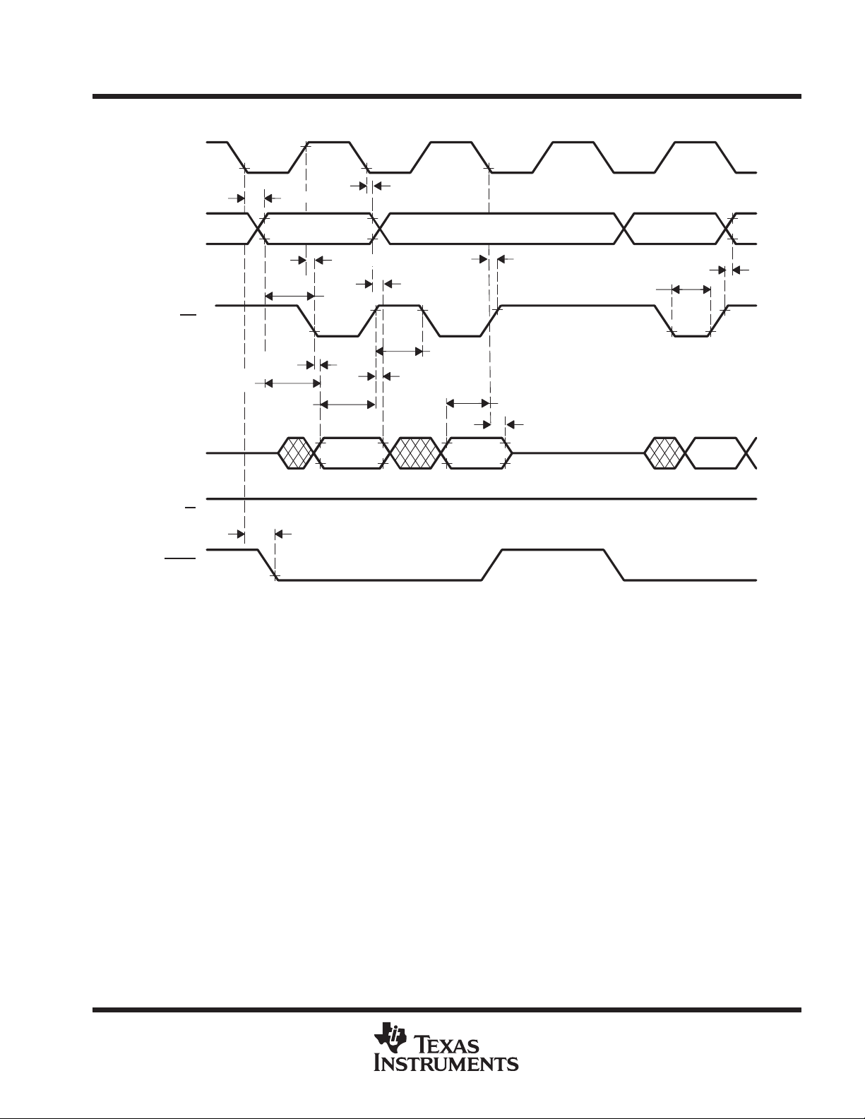
TMS320C203, TMS320C209, TMS320LC203
DIGITAL SIGNAL PROCESSORS
SPRS025B – JUNE 1995 – REVISED AUGUST 1998
MEMORY AND PERIPHERAL INTERFACE TIMING FOR ’C203/’LC203 (CONTINUED)
CLKOUT1
t
h(COL-A)RD
A0–A15
t
d(COL–A)
RD
D0–D15
(data in)
R/W
STRB
t
d(CO–RD)
t
su(D–COL)RD
t
h(COL-D)RD
t
w(RDL)
t
a(A)
t
a(RD)
t
su(D-RD)
t
su(A-RD)
t
d(COL–S)
t
d(CO–RD)
t
h(AIV-D)
t
h(RD-D)
t
w(RDH)
Figure 10. Memory Interface Read Timing for TMS320C203/LC203
t
h(RD-A)
POST OFFICE BOX 1443 • HOUSTON, TEXAS 77251–1443
53
Page 54

TMS320C203, TMS320C209, TMS320LC203
SYMBOLS
DIGITAL SIGNAL PROCESSORS
SPRS025B – JUNE 1995 – REVISED AUGUST 1998
memory and parallel I/O interface
write
timing for TMS320C203 @ 5 V
A15–A0, PS, DS, IS, R/W, and BR timings are all included in the timings referenced to A15–A0 except when
in transition between read and write operations, where PS
, DS, and IS pulse high [see t
w(NSN)
].
switching characteristics over recommended operating conditions @ 5 V [H = 0.5t
(see Figure 11)
PARAMETER
t
su(A-W)
t
h(W-A)
t
su(A-COL)
t
h(COL-A)W
t
w(MS)
t
w(WL)
t
w(WH)
t
d(COL-W)
t
d(RD-W)
t
d(W-RD)
t
su(D-W)
t
h(W-D)
t
su(D-COL)W
t
h(COL-D)W
t
en(D-W)
†
Values derived from characterization data and not tested
Setup time, address valid before WE low t
Hold time, address valid after WE high t
Setup time, write address valid before CLKOUT1 low t
Hold time, write address valid after CLKOUT1 low t
Pulse duration, IS, DS, PS inactive high
Pulse duration, WE low (no wait states) 2H – 3 2H + 2 2H – 4 2H + 2 ns
Pulse duration, WE high 2H – 2 2H – 2 ns
Delay time, CLKOUT1 low to WE low/high – 1 6 – 1 4 ns
Delay time, RD high to WE low t
Delay time, WE high to RD low t
Setup time, write data valid before WE high t
Hold time, write data valid after WE high t
Setup time, write data valid before CLKOUT1 low t
Hold time, write data valid after CLKOUT1 low t
Enable time, data bus driven from WE
ALTERNATE
su(A)W
h(A)W
su(A)CO
†
†
h(A)COLW
t
w(NSN)
d(RDW)
d(WRD)
su(D)W
h(D)W
su(DCOL)W
h(DCOL)W
t
en(D)W
’320C203-40
’320C203-57
MIN MAX MIN MAX
H – 7 H – 6 ns
H – 10 H – 8 ns
H – 9 H – 8 ns
H – 3 H – 5 ns
H – 9 H – 8 ns
2H – 8 2H – 7 ns
3H – 8 3H – 8 ns
2H – 15 2H†2H – 14 2H
H – 4 H + 7
2H – 20 2H†2H – 20 2H
H – 4 H + 11
– 4 – 3 ns
†
†
’320C203-80
H – 3 H + 7
H – 5 H + 11
†
†
†
†
c(CO)
UNIT
ns
ns
ns
ns
]
54
POST OFFICE BOX 1443 • HOUSTON, TEXAS 77251–1443
Page 55

PARAMETER
UNIT
TMS320C203, TMS320C209, TMS320LC203
DIGITAL SIGNAL PROCESSORS
SPRS025B – JUNE 1995 – REVISED AUGUST 1998
memory and parallel I/O interface
write
timing for TMS320LC203 @ 3.3 V
A15–A0, PS, DS, IS, R/W, and BR timings are all included in the timings referenced to A15–A0 except when
in transition between read and write operations, where PS
, DS, and IS pulse high [see t
w(NSN)
].
switching characteristics over recommended operating conditions @ 3.3 V [H = 0.5t
(see Figure 11)
’320LC203-40
MIN MAX
H – 5 ns
H – 10 ns
H – 9 ns
H – 5 ns
H – 9 ns
2H – 8 ns
3H – 8 ns
2H – 15 2H
H – 4 H + 7
2H – 20 2H
H – 4 H + 11
– 4 ns
†
†
†
†
t
su(A-W)
t
h(W-A)
t
su(A-COL)
t
h(COL-A)W
t
w(MS)
t
w(WL)
t
w(WH)
t
d(COL-W)
t
d(RD-W)
t
d(W-RD)
t
su(D-W)
t
h(W-D)
t
su(D-COL)W
t
h(COL-D)W
t
en(D-W)
†
Values derived from characterization data and not tested
Setup time, address valid before WE low t
Hold time, address valid after WE high t
Setup time, write address valid before CLKOUT1 low t
Hold time, write address valid after CLKOUT1 low t
Pulse duration, IS, DS, PS inactive high
Pulse duration, WE low (no wait states) 2H – 3 2H + 1 ns
Pulse duration, WE high 2H – 2 ns
Delay time, CLKOUT1 low to WE low/high – 1 6 ns
Delay time, RD high to WE low t
Delay time, WE high to RD low t
Setup time, write data valid before WE high t
Hold time, write data valid after WE high t
Setup time, write data valid before CLKOUT1 low t
Hold time, write data valid after CLKOUT1 low t
Enable time, data bus driven from WE
ALTERNATE
SYMBOLS
su(A)W
h(A)W
su(A)CO
†
†
h(A)COLW
t
w(NSN)
d(RDW)
d(WRD)
su(D)W
h(D)W
su(DCOL)W
h(DCOL)W
t
en(D)W
c(CO)
ns
ns
ns
ns
]
POST OFFICE BOX 1443 • HOUSTON, TEXAS 77251–1443
55
Page 56

TMS320C203, TMS320C209, TMS320LC203
DIGITAL SIGNAL PROCESSORS
SPRS025B – JUNE 1995 – REVISED AUGUST 1998
MEMORY AND PERIPHERAL INTERFACE TIMING FOR ’C203/’LC203 (CONTINUED)
CLKOUT1
RD
STRB
IS, DS
or PS
A0–A15
R/W
WE
t
t
su(A-W)
d(RD-W)
t
w(WL)
t
en(D-W)
t
h(COL-A)W
t
d(COL-W)
t
su(D-W)
t
h(W-D)
t
su(A-COL)
t
d(COL-W)
t
w(WH)
t
d(W-RD)
t
h(W-A)
t
su(D-COL)W
t
h(COL-D)W
t
w(MS)
56
D0–D15
(data out)
Figure 11. Memory Interface Write Timing for TMS320C203/LC203
POST OFFICE BOX 1443 • HOUSTON, TEXAS 77251–1443
Page 57

SYMBOL
UNIT
TMS320C203, TMS320C209, TMS320LC203
DIGITAL SIGNAL PROCESSORS
SPRS025B – JUNE 1995 – REVISED AUGUST 1998
READY timing
timing requirements over recommended operating conditions for TMS320C203 @ 5 V
(see Figure 12)
’320C203-40
’320C203-57
MIN MAX MIN MAX
14 14 ns
4 4 ns
H – 14 H – 14 ns
H + 4 H + 3 ns
H – 17 H – 16 ns
2H – 18 2H – 16 ns
t
su(R-CO)
t
h(CO-R)
t
su(R-RD)
t
h(RD-R)
t
v(R-W)
t
h(W-R)
t
v(R-A)RD
t
v(R-A)W
ALTERNATE
Setup time, READY before CLKOUT1 rising edge 11 11 ns
Hold time, READY after CLKOUT1 rising edge 0 0 ns
Setup time, READY before RD falling edge t
Hold time, READY after RD falling edge t
Valid time, READY after WE falling edge t
Hold time, READY after WE falling edge t
Valid time, READY after address valid on read t
Valid time, READY after address valid on write t
su(R)RD
h(R)RD
v(R)W
h(R)W
v(R)ARD
v(R)AW
timing requirements over recommended operating conditions for TMS320LC203 @ 3.3 V
(see Figure 12)
ALTERNATE
SYMBOL
t
su(R-CO)
t
h(CO-R)
t
su(R-RD)
t
h(RD-R)
t
v(R-W)
t
h(W-R)
t
v(R-A)RD
t
v(R-A)W
Setup time, READY before CLKOUT1 rising edge 17 ns
Hold time, READY after CLKOUT1 rising edge 0 ns
Setup time, READY before RD falling edge t
Hold time, READY after RD falling edge t
Valid time, READY after WE falling edge t
Hold time, READY after WE falling edge t
Valid time, READY after address valid on read t
Valid time, READY after address valid on write t
su(R)RD
h(R)RD
v(R)W
h(R)W
v(R)ARD
v(R)AW
’320C203-80
’320LC203-40
MIN MAX
22 ns
4 ns
H – 23 ns
H + 4 ns
H – 22 ns
2H – 21 ns
UNIT
CLKOUT1
RD
WE
READY
A0–A15
t
su(R-CO)
t
su(R-RD)
t
v(R-A)RD
t
h(CO-R)
t
h(RD-R)
t
v(R-A)W
t
h(W-R)
t
v(R-W)
Figure 12. READY Timing for TMS320C203/LC203
POST OFFICE BOX 1443 • HOUSTON, TEXAS 77251–1443
57
Page 58

TMS320C203, TMS320C209, TMS320LC203
SYMBOL
SYMBOL
DIGITAL SIGNAL PROCESSORS
SPRS025B – JUNE 1995 – REVISED AUGUST 1998
XF, TOUT, RS, INT1 – INT3, NMI, and BIO timing
switching characteristics over recommended operating conditions for TMS320C203 @ 5 V
(see Figure 13)
’320C203-40
’320C203-57
MIN MAX MIN MAX
†
0
†
0
PARAMETER
t
d(COH-XF)
t
d(COH-TOUT)
t
w(TOUT)
†
Values derived from characterization data and not tested
Delay time, CLKOUT1 high to XF valid t
Delay time, CLKOUT1 high to TOUT high/low t
Pulse duration, TOUT high 2H – 12 2H – 9 ns
ALTERNATE
d(XF)
d(TOUT)
timing requirements over recommended operating conditions for TMS320C203 @ 5 V
[H = 0.5t
t
su(RS-CIL)
t
su(RS-COL)
t
w(RSL)
t
d(RS-RST)
t
su(IN-COLS)
t
h(COLS-IN)
t
w(IN)
t
d(IN-INT)
‡
This parameter assumes the CLKOUT1 to be stable before RS goes active.
] (see Figure 14 and Figure 15)
c(CO)
ALTERNATE
Setup time, RS before CLKIN low t
Setup time, RS before CLKOUT1 low t
Pulse duration, RS low
Delay time, RS high to reset-vector fetch t
Setup time, INTN before CLKOUT1 low (synchronous) t
Hold time, INTN after CLKOUT1 low (synchronous) t
Pulse duration, INTN low 2H + 18 2H + 16 ns
Delay time, INTN low to interrupt-vector fetch t
‡
su(RS)CIL
su(RS)COL
d(EX)
su(IN)COL
h(IN)COL
d(IN)
’320C203-40
’320C203-57
MIN MAX MIN MAX
11 9 ns
14 11 ns
12H 12H ns
34H 34H ns
10 10 ns
1 1 ns
12H 12H ns
13 0
†
11
’320C203-80
†
†
0
’320C203-80
UNIT
10 ns
11 ns
UNIT
CLKOUT1
XF
TOUT
t
d(COH-XF)
t
d(COH-TOUT)
t
w(TOUT)
Figure 13. XF and TOUT Timing for TMS320C203/LC203
58
POST OFFICE BOX 1443 • HOUSTON, TEXAS 77251–1443
Page 59

PARAMETER
UNIT
UNIT
TMS320C203, TMS320C209, TMS320LC203
DIGITAL SIGNAL PROCESSORS
SPRS025B – JUNE 1995 – REVISED AUGUST 1998
XF, TOUT, RS, INT1 – INT3, NMI, and BIO timing (continued)
switching characteristics over recommended operating conditions for TMS320LC203 @ 3.3 V
(see Figure 13)
ALTERNATE
SYMBOL
t
d(COH-XF)
t
d(COH-TOUT)
t
w(TOUT)
†
Values derived from characterization data and not tested
Delay time, CLKOUT1 high to XF valid t
Delay time, CLKOUT1 high to TOUT high/low t
Pulse duration, TOUT high 2H – 12 ns
d(XF)
d(TOUT)
timing requirements over recommended operating conditions for TMS320LC203 @ 3.3 V
[H = 0.5t
t
su(RS-CIL)
t
su(RS-COL)
t
w(RSL)
t
d(RS-RST)
t
su(IN-COLS)
t
h(COLS-IN)
t
w(IN)
t
d(IN-INT)
‡
This parameter assumes the CLKOUT1 to be stable before RS goes active.
] (see Figure 14 and Figure 15)
c(CO)
ALTERNATE
SYMBOL
Setup time, RS before CLKIN low t
Setup time, RS before CLKOUT1 low t
Pulse duration, RS low
Delay time, RS high to reset-vector fetch t
Setup time, INTN before CLKOUT1 low (synchronous) t
Hold time, INTN after CLKOUT1 low (synchronous) t
Pulse duration, INTN low 2H + 18 ns
Delay time, INTN low to interrupt-vector fetch t
‡
su(RS)CIL
su(RS)COL
d(EX)
su(IN)COL
h(IN)COL
d(IN)
’320LC203-40
MIN MAX
†
0
†
0
’320LC203-40
MIN MAX
11 ns
15 ns
12H ns
34H ns
10 ns
1 ns
12H ns
12 ns
15 ns
POST OFFICE BOX 1443 • HOUSTON, TEXAS 77251–1443
59
Page 60

TMS320C203, TMS320C209, TMS320LC203
DIGITAL SIGNAL PROCESSORS
SPRS025B – JUNE 1995 – REVISED AUGUST 1998
XF, TOUT, RS, INT1 – INT3, NMI, and BIO timing (continued)
CLKIN/X2
RS
CLKOUT1
A0–A15
t
su(RS-CIL)
t
w(RSL)
t
d(RS-RST)
t
su(RS-COL)
Figure 14. Reset Timing for TMS320C203/LC203
CLKOUT1
t
su(IN-COLS)
†
INTN
†
INTN: BIO, INT1 – INT3, NMI
t
w(IN)
t
h(COLS-IN)
Figure 15. Interrupts and BIO Timing for TMS320C203/LC203
60
POST OFFICE BOX 1443 • HOUSTON, TEXAS 77251–1443
Page 61
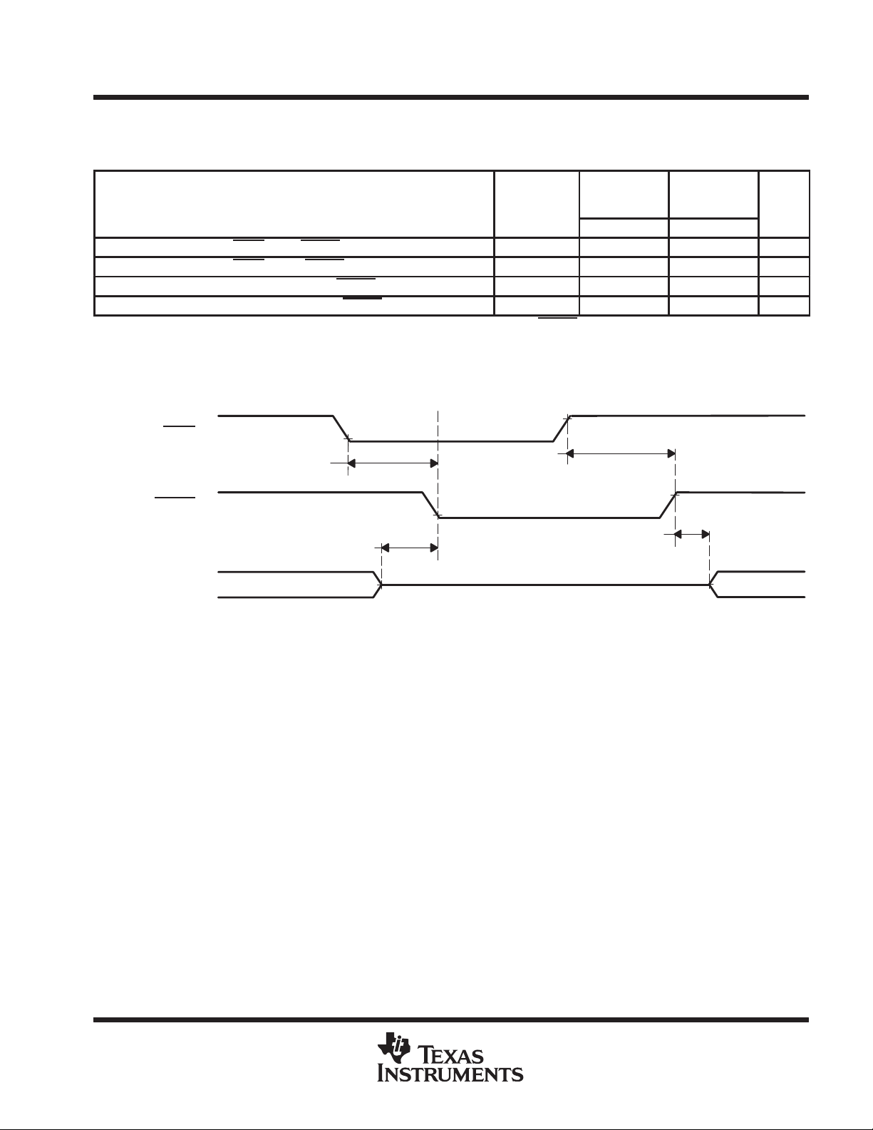
external DMA timing
TMS320C203, TMS320C209, TMS320LC203
DIGITAL SIGNAL PROCESSORS
SPRS025B – JUNE 1995 – REVISED AUGUST 1998
switching characteristics over recommended operating conditions [H = 0.5t
’320C203-40
PARAMETER
t
d(HL-HAL)
t
d(HH-HAH)
t
hz(M-HAL)
t
en(HAH-M)
†
The delay values will change based on the software logic (IDLE instruction) that activates HOLDA. See the
number SPRU127) for functional description of HOLD logic.
‡
This parameter includes all memory control lines.
§
Values derived from characterization data and not tested
Delay time, HOLD low to HOLDA low
Delay time, HOLD high to HOLDA high
Address high impedance before HOLDA low
Enable time, address driven from HOLDA high
HOLD
t
d(HL-HAL)
HOLDA
t
hz(M-HAL)
†
†
‡§
§
ALTERNATE
SYMBOL
t
z(M-HAL)
t
d(HH-HAH)
’320C203-57
’320LC203-40
MIN MAX MIN MAX
4H 4H ns
2H 2H ns
H – 15 H – 10 ns
H – 5 H – 4 ns
TMS320C2xx User’s Guide
t
en(HAH-M)
] (see Figure 16)
c(CO)
’320C203-80
UNIT
(literature
Address Bus
Control Signals
Figure 16. External DMA Timing for ’C203/’LC203
POST OFFICE BOX 1443 • HOUSTON, TEXAS 77251–1443
61
Page 62

TMS320C203, TMS320C209, TMS320LC203
DIGITAL SIGNAL PROCESSORS
SPRS025B – JUNE 1995 – REVISED AUGUST 1998
serial-port receive timing
timing requirements over recommended ranges of supply voltage and operating free-air
temperature [H = 0.5t
t
c(CLKR)
t
f(CLKR)
t
r(CLKR)
t
w(CLKR)
t
su(FR-CLKR)
t
su(DR-CLKR)
t
h(CLKR-FR)
t
h(CLKR-DR)
†
Values derived from characterization data and not tested
Cycle time, serial-port clock (CLKR) t
Fall time, serial-port clock† (CLKR) t
Rise time, serial-port clock† (CLKR) t
Pulse duration, serial-port clock (CLKR) low/high t
Setup time, FSR before CLKR falling edge t
Setup time, DR before CLKR falling edge t
Hold time, FSR after CLKR falling edge t
Hold time, DR after CLKR falling edge t
] (see Figure 17)
c(CO)
t
c(CLKR)
t
w(CLKR)
ALTERNATE
SYMBOL
c(SCK)
f(SCK)
r(SCK)
w(SCK)
su(FS)
su(DR)
h(FS)
h(DR)
t
f(CLKR)
’320C203-40
’320C203-57
’320LC203-40
MIN MAX MIN MAX
4H 4H ns
2H 2H ns
10 7 ns
10 7 ns
10 7 ns
10 7 ns
’320C203-80
8 6 ns
8 6 ns
UNIT
CLKR
FSR
DR
t
h(CLKR-FR)
t
su(FR-CLKR)
t
1 2 15/7 16/8
t
w(CLKR)
t
su(DR-CLKR)
t
h(CLKR-DR)
r(CLKR)
Figure 17. Serial-Port Receive Timing for ’C203/’LC203
62
POST OFFICE BOX 1443 • HOUSTON, TEXAS 77251–1443
Page 63

TMS320C203, TMS320C209, TMS320LC203
DIGITAL SIGNAL PROCESSORS
serial-port transmit timing of external clocks and external frames
SPRS025B – JUNE 1995 – REVISED AUGUST 1998
switching characteristics over recommended operating conditions (see Figure 18) [H = 0.5t
’320C203-40
PARAMETER
t
d(CLKX-DX)
t
dis(DX-CLKX)
t
h(CLKX-DX)
t
c(CLKX)
t
f(CLKX)
t
r(CLKX)
t
w(CLKX)
t
d(CLKX-FX)
t
h(CLKXL-FX)
t
h(CLKXH-FX)
†
Values derived from characterization data and not tested
CLKX
FSX
DX
Delay time, CLKX high to DX valid t
Disable time, DX valid from CLKX high
Hold time, DX valid after CLKX high t
Cycle time, serial-port clock (CLKX) t
Fall time, serial-port clock† (CLKX) t
Rise time, serial-port clock† (CLKX) t
Pulse duration, serial-port clock (CLKX) low/high t
Delay time, CLKX rising edge to FSX t
Hold time, FSX after CLKX falling edge low t
Hold time, FSX after CLKX rising edge
t
c(CLKX)
t
d(CLKX-FX)
t
h(CLKXH-FX)
t
h(CLKXL-FX)
t
d(CLKX-DX)
1 2 15/7 16/8
†
†
t
w(CLKX)
d(DX)
t
dis(DX)
h(DX)
c(SCK)
f(SCK)
r(SCK)
w(SCK)
d(FS)
h(FS)
t
h(FS)H
t
w(CLKX)
t
h(CLKX-DX)
ALTERNATE
SYMBOL
t
f(CLKX)
’320C203-57
’320LC203-40
MIN MAX MIN MAX
– 5 – 5 ns
4H 4H ns
2H 2H ns
2H – 8 2H – 8 ns
10 7 ns
2H – 8 2H – 8 ns
t
r(CLKX)
’320C203-80
†
25 25 ns
40 40 ns
8 6 ns
8 6 ns
t
dis(DX-CLKX)
c(CO)
UNIT
]
Figure 18. Serial-Port Transmit Timing of External Clocks and External Frames for ’C203/’LC203
POST OFFICE BOX 1443 • HOUSTON, TEXAS 77251–1443
63
Page 64

TMS320C203, TMS320C209, TMS320LC203
DIGITAL SIGNAL PROCESSORS
SPRS025B – JUNE 1995 – REVISED AUGUST 1998
serial-port transmit timing of internal clocks and internal frames
switching characteristics over recommended operating conditions [H = 0.5t
’320C203-40
PARAMETER
t
d(CLKX-DX)
t
dis(DX-CLKX)
t
h(CLKX-DX)
t
c(CLKX)
t
f(CLKX)
t
r(CLKX)
t
w(CLKX)
t
d(CLKX-FX)
t
h(CLKXH-FX)
†
Values derived from characterization data and not tested
CLKX
Delay time, CLKX high to DX valid t
Disable time, DX valid from CLKX high
Hold time, DX valid after CLKX high t
Cycle time, serial-port clock (CLKX) t
Fall time, serial-port clock† (CLKX) t
Rise time, serial-port clock† (CLKX) t
Pulse duration, serial-port clock (CLKX) low/high t
Delay time, CLKX rising edge to FSX t
Hold time, FSX after CLKX rising edge
t
c(CLKX)
t
d(CLKX-FX)
t
h(CLKXH-FX)
†
†
t
w(CLKX)
ALT
SYMBOL
d(DX)
t
dis(DX)
h(DX)
c(SCK)
f(SCK)
r(SCK)
w(SCK)
d(FS)
t
h(FS)H
t
w(CLKX)
’320C203-57
’320LC203-40
MIN TYP MAX MIN TYP MAX
25 18 ns
†
40
†
0
4H 4H ns
5 4 ns
5 4 ns
†
2H – 8
†
– 5
†
– 5
t
f(CLKX)
t
r(CLKX)
25 – 4
] (see Figure 19)
c(CO)
’320C203-80
†
0
†
2H – 6
†
†
– 5
UNIT
29†ns
ns
ns
18 ns
ns
FSX
t
d(CLKX-DX)
DX
1 2 15/7 16/8
t
h(CLKX-DX)
t
dis(DX-CLKX)
Figure 19. Serial-Port Transmit Timing of Internal Clocks and Internal Frames for ’C203/’LC203
64
POST OFFICE BOX 1443 • HOUSTON, TEXAS 77251–1443
Page 65

CLKIN/X2
3
V
3
VIHHigh-level in ut voltage
V
TMS320C203, TMS320C209, TMS320LC203
DIGITAL SIGNAL PROCESSORS
SPRS025B – JUNE 1995 – REVISED AUGUST 1998
absolute maximum ratings over case temperature range (unless otherwise noted) (’320C209 only)
Supply voltage range, V
Input voltage range – 0.3 V to 7 V. . . . . . . . . . . . . . . . . . . . . . . . . . . . . . . . . . . . . . . . . . . . . . . . . . . . . . . . . . . . . . . .
Output voltage range – 0.3 V to 7 V. . . . . . . . . . . . . . . . . . . . . . . . . . . . . . . . . . . . . . . . . . . . . . . . . . . . . . . . . . . . . . .
Operating free-air temperature range, T
Storage temperature range, T
†
Stresses beyond those listed under “absolute maximum ratings” may cause permanent damage to the device. These are stress ratings only, and
functional operation of the device at these or any other conditions beyond those indicated under “recommended operating conditions” is not
implied. Exposure to absolute-maximum-rated conditions for extended periods may affect device reliability.
NOTE 1: All voltage values are with respect to VSS.
(see Note 1) – 0.3 V to 7 V. . . . . . . . . . . . . . . . . . . . . . . . . . . . . . . . . . . . . . . . . . . . . .
DD
0°C to 85°C. . . . . . . . . . . . . . . . . . . . . . . . . . . . . . . . . . . . . . . . . . . . . .
– 55°C to 150°C. . . . . . . . . . . . . . . . . . . . . . . . . . . . . . . . . . . . . . . . . . . . . . . . . .
stg
C
recommended operating conditions for TMS320C209 @ 5 V
TEST CONDITIONS MIN NOM MAX UNIT
V
V
V
I
I
T
DD
SS
IL
OH
OL
C
Supply voltage 5-V operation 4.5 5 5.5 V
Supply voltage 0 V
+ 0.
p
Low-level input voltage
High-level output current – 300 µA
Low-level output current 2 mA
Case temperature 0 85 °C
Inputs 2.0 VDD + 0.3
CLKIN/X2 – 0.3 0.7
RS
All other inputs – 0.3 0.8
DD
0.8
V
†
electrical characteristics over recommended ranges of supply voltage and operating case
temperature for TMS320C209 @ 5 V
PARAMETER TEST CONDITIONS MIN TYP MAX UNIT
V
V
I
I
I
C
C
I
OZ
DD
High-level output voltage 5-V operation, IOH = MAX 2.4 V
OH
Low-level output voltage 5-V operation, IOL = MAX 0.6 V
OL
Input current VI = VDD or 0 V – 10 10 µA
Output current, high-impedance state (off-state) VO = VDD or 0 V ± 5 µA
Supply current, core CPU 5-V operation, 57 MHz 76 mA
Input capacitance 15 pF
i
Output capacitance 15 pF
o
POST OFFICE BOX 1443 • HOUSTON, TEXAS 77251–1443
65
Page 66

TMS320C203, TMS320C209, TMS320LC203
DIGITAL SIGNAL PROCESSORS
SPRS025B – JUNE 1995 – REVISED AUGUST 1998
PARAMETER MEASUREMENT INFORMATION FOR ’C209
Tester Pin
Electronics
I
OL
V
LOAD
Where: I
OL
I
OH
V
LOAD
C
T
50 Ω
C
T
I
OH
= 2 mA (all outputs)
= 300 µA (all outputs)
= 1.5 V
= 60-pF typical load-circuit capacitance
Output
Under
Test
Figure 20. Test Load Circuit
signal-transition levels
The data in this section is shown for the 5-V version (’C209). Note that some of the signals use different
reference voltages, see the recommended operating conditions table for 5-V devices. TTL-output levels are
driven to a minimum logic-high level of 2.4 V and to a maximum logic-low level of 0.6 V.
Figure 5 shows the TTL-level outputs.
2.4 V
80%
20%
0.6 V
Figure 21. TTL-Level Outputs
TTL-output transition times are specified as follows:
D
For a
high-to-low transition
, the level at which the output is said to be no longer high is below 80% of the
total voltage range and lower and the level at which the output is said to be low is 20% of the total voltage
range and lower.
D
For a
low-to-high transition
, the level at which the output is said to be no longer low is 20% of the total voltage
range and higher and the level at which the output is said to be high is 80% of the total voltage range and
higher.
66
POST OFFICE BOX 1443 • HOUSTON, TEXAS 77251–1443
Page 67

PARAMETER MEASUREMENT INFORMATION FOR ’C209
Figure 6 shows the TTL-level inputs.
Figure 22. TTL-Level Inputs
TTL-compatible input transition times are specified as follows:
D
For a
high-to-low transition
of the total voltage range and lower and the level at which the input is said to be low is 10% of the total voltage
range and lower.
D
For a
low-to-high transition
of the total voltage range and higher and the level at which the input is said to be high is 90% of the total
voltage range and higher.
on an input signal, the level at which the input is said to be no longer high is 90%
on an input signal, the level at which the input is said to be no longer low is 10%
TMS320C203, TMS320C209, TMS320LC203
DIGITAL SIGNAL PROCESSORS
SPRS025B – JUNE 1995 – REVISED AUGUST 1998
2.0 V
90%
10%
0.7 V
POST OFFICE BOX 1443 • HOUSTON, TEXAS 77251–1443
67
Page 68

TMS320C203, TMS320C209, TMS320LC203
DIGITAL SIGNAL PROCESSORS
SPRS025B – JUNE 1995 – REVISED AUGUST 1998
PARAMETER MEASUREMENT INFORMATION FOR ’C209
timing parameter symbology
Timing parameter symbols used are created in accordance with JEDEC Standard 100-A. To shorten the
symbols, some of the pin names and other related terminology have been abbreviated as follows:
A Address or A[15:0] R READY
CI CLKIN/X2 RD Read cycle or RD
CO CLKOUT1 RS RESET pins RS or RS
D Data or D[15:0] S STRB
FS FSX SCK Serial-port clock
IN INTN; BIO
MS Memory strobe pins IS, DS, or PS
Lowercase subscripts and their meanings are: The following letters and symbols and their meanings are:
a access time H High
c cycle time (period) L Low
d delay time V Valid
dis disable time Z High impedance
en enable time X Unknown, changing, or don’t care level
f fall time
h hold time
r rise time
su setup time
t transition time
v valid time
w pulse duration (width)
, INT1–INT3, NMI W Write cycle or WE
general notes on timing parameters for ’C209
All output signals from the TMS320C2xx devices (including CLKOUT1) are derived from an internal clock such
that all output transitions for a given half cycle occur with a minimum of skewing relative to each other.
The signal combinations shown in the following timing diagrams may not necessarily represent actual cycles.
For actual cycle examples, refer to the appropriate cycle description section of this data sheet.
68
POST OFFICE BOX 1443 • HOUSTON, TEXAS 77251–1443
Page 69

TMS320C203, TMS320C209, TMS320LC203
DIGITAL SIGNAL PROCESSORS
SPRS025B – JUNE 1995 – REVISED AUGUST 1998
CLOCK CHARACTERISTICS AND TIMING FOR ’C209
TMS320C209 clock options
PARAMETER CLKMOD
Internal divide-by-two with external crystal 0
PLL multiply-by-two 1
internal divide-by-two clock option with external crystal
The internal oscillator is enabled by connecting a crystal across X1 and CLKIN/X2. The frequency of CLKOUT1
is one-half the crystal’s oscillating frequency . The crystal should be in either fundamental or overtone operation
and parallel resonant, with an effective series resistance of 30 Ω and a power dissipation of 1 mW; it should be
specified at a load capacitance of 20 pF. Note that overtone crystals require an additional tuned-LC circuit.
Figure 23 shows an external crystal (fundamental frequency) connected to the on-chip oscillator.
X1 CLKIN/X2
Crystal
C1 C2
Figure 23. Internal Clock Option
POST OFFICE BOX 1443 • HOUSTON, TEXAS 77251–1443
69
Page 70

TMS320C203, TMS320C209, TMS320LC203
†
PARAMETER
UNIT
UNIT
(CO)
DIGITAL SIGNAL PROCESSORS
SPRS025B – JUNE 1995 – REVISED AUGUST 1998
timing at VDD = 5 V with the PLL circuit disabled, divide-by-two mode for TMS320C209
PARAMETER TEST CONDITIONS MIN MAX UNIT
f
Input clock frequency TC = 0°C to 85°C, 5 V 0
x
†
This device is implemented in static logic and therefore can operate with t
approaching 0 Hz, but is tested at fx = 6.7 MHz to meet device test time requirements.
approaching ∞. The device is characterized at frequencies
c(CI)
†
57 MHz
switching characteristics over recommended operating conditions for TMS320C209
(see Figure 24)
’320C209-57
MIN TYP MAX
t
c(CO)
t
d(CIH-CO)
t
f(CO)
t
r(CO)
t
w(COL)
t
w(COH)
‡
This device is implemented in static logic and therefore can operate with t
approaching 0 Hz, but is tested at t
Cycle time, CLKOUT1 35 2t
Delay time, CLKIN high to CLKOUT1 high/low 1 11 20 ns
Fall time, CLKOUT1 5 ns
Rise time, CLKOUT1 5 ns
Pulse duration, CLKOUT1 low H – 2 H H + 2 ns
Pulse duration, CLKOUT1 high H – 2 H H + 2 ns
= 300 ns to meet device test time requirements.
c(CI)
c(CI)
approaching ∞. The device is characterized at frequencies
c(CI)
‡
ns
timing requirements over recommended operating conditions for TMS320C209 (see Figure 24)
’320C209-57
MIN MAX
t
c(CI)
t
f(CI)
t
r(CI)
t
w(CIL)
t
w(CIH)
§
Values derived from characterization data and not tested
¶
This device is implemented in static logic and therefore can operate with t
approaching 0 Hz, but is tested at a minimum t
Cycle time, CLKIN 17.5
Fall time, CLKIN
Rise time, CLKIN
Pulse duration, CLKIN low 8
Pulse duration, CLKIN high 8
§
§
= 150 ns to meet device test time requirements.
c(CI)
approaching ∞. The device is characterized at frequencies
c(CI)
¶
ns
5 ns
5 ns
¶
ns
¶
ns
CLKIN
CLKOUT1
70
t
t
c(CI)
t
d(CIH-CO)
t
f(CI)
t
c(CO)
w(CIH)
t
w(COL)
t
w(CIL)
t
r(CI)
t
r(CO)
t
w(COH)
t
f
Figure 24. CLKIN-to-CLKOUT1 Timing Without PLL (using ÷2 clock option) for TMS320C209
POST OFFICE BOX 1443 • HOUSTON, TEXAS 77251–1443
Page 71

PARAMETER
UNIT
UNIT
t
TMS320C203, TMS320C209, TMS320LC203
DIGITAL SIGNAL PROCESSORS
SPRS025B – JUNE 1995 – REVISED AUGUST 1998
timing @ VDD = 5 V with the PLL circuit enabled, multiply-by-two mode for TMS320C209
PARAMETER TEST CONDITIONS MIN MAX UNIT
f
x
switching characteristics over recommended operating conditions for TMS320C209 @ 5 V
(see Figure 25)
t
c(CO)
t
d(CIH-CO)
t
f(CO)
t
r(CO)
t
w(COL)
t
w(COH)
t
p
†
Values derived from characterization data and not tested
Input clock frequency TC = 0°C to 85°C, 5 V 5 14.25 MHz
’320C209-57
MIN TYP MAX
Cycle time, CLKOUT1 35 75 ns
Delay time, CLKIN high to CLKOUT1 high/low 3 8 18 ns
Fall time, CLKOUT1
Rise time, CLKOUT1
Pulse duration, CLKOUT1 low H – 2 H H + 2 ns
Pulse duration, CLKOUT1 high H – 2 H H + 2 ns
Transition time, PLL synchronized after CLKIN supplied 1000 cycles
†
†
5 ns
5 ns
timing requirements over recommended operating conditions for TMS320C209 @ 5 V
(see Figure 25)
’320C209-57
MIN MAX
c(CI)
t
f(CI)
t
r(CI)
t
w(CIL)
t
w(CIH)
†
Values derived from characterization data and not tested
CLKIN
Cycle time, CLKIN multiply-by-one 35 75 ns
Cycle time, CLKIN multiply-by-two 70 200 ns
Fall time, CLKIN
Rise time, CLKIN
Pulse duration, CLKIN low 14 95 ns
Pulse duration, CLKIN high 14 95 ns
†
†
t
d(CIH–CO)
t
c(CO)
t
c(CI)
t
w(COH)
t
w(CIH)
t
w(COL)
t
f(CI)
t
f(CO)
t
w(CIL)
t
r(CO)
4 ns
4 ns
t
r(CI)
CLKOUT1
Figure 25. CLKIN-to-CLKOUT1 Timing With PLL (using ×2 clock option) for TMS320C209
POST OFFICE BOX 1443 • HOUSTON, TEXAS 77251–1443
71
Page 72

TMS320C203, TMS320C209, TMS320LC203
PARAMETER
UNIT
UNIT
DIGITAL SIGNAL PROCESSORS
SPRS025B – JUNE 1995 – REVISED AUGUST 1998
MEMORY AND PERIPHERAL INTERFACE TIMING
memory and parallel I/O interface
read
timing for TMS320C209 @ 5 V
A15–A0, PS, DS, IS, R/W, and BR timings are all included in the timings referenced to A15–A0 except when
in transition between read and write operations, where PS
switching characteristics over recommended operating conditions [H = 0.5t
t
su(A-RD)
t
h(RD-A)
t
d(COL-A)
t
h(COL-A)RD
t
d(CO-RD)
t
d(COL-S)
t
w(RDL)
t
w(RDH)
t
d(RD-W)
†
Values derived from characterization data and not tested
Setup time, address valid before RD low t
Hold time, address valid after RD high t
Delay time, CLKOUT1 low to read address valid 8 ns
Hold time, read address valid after CLKOUT1 low t
Delay time, CLKOUT1 high/low to RD low/high 0 6 ns
Delay time, CLKOUT1 low to STRB low/high
Pulse duration, RD low (no wait states) H – 3 H + 2 ns
Pulse duration, RD high H – 4 H + 2 ns
Delay time, RD high to WE low t
†
timing requirements over recommended operating conditions [H = 0.5t
t
a(A)
t
su(D-RD)
t
h(RD-D)
t
h(AIV-D)
t
su(D-COL)RD
t
h(COL-D)RD
t
a(RD)
Access time, from address valid to read data 2H – 15 ns
Setup time, read data before RD high t
Hold time, read data after RD high t
Hold time, read data after address invalid t
Setup time, read data before CLKOUT1 low t
Hold time, read data after CLKOUT1 low t
Access time, from RD low to read data H – 12 ns
, DS, and IS pulse high [see t
c(CO)
ALTERNATE
SYMBOLS
su(A)RD
h(A)RD
h(A)COLRD
d(RDW)
] (see Figure 26)
c(CO)
ALTERNATE
SYMBOLS
su(D)RD
h(D)RD
h(D)A
su(DCOL)RD
h(DCOL)RD
w(NSN)
].
] (see Figure 26)
’320C209-57
MIN MAX
H – 5 ns
– 6 ns
– 2 ns
0 5 ns
2H – 8 ns
’320C209-57
MIN MAX
13 ns
– 2 ns
0 ns
9 ns
– 1 ns
72
POST OFFICE BOX 1443 • HOUSTON, TEXAS 77251–1443
Page 73

TMS320C203, TMS320C209, TMS320LC203
DIGITAL SIGNAL PROCESSORS
SPRS025B – JUNE 1995 – REVISED AUGUST 1998
memory and parallel I/O interface read timing for TMS320C209 @ 5 V (continued)
CLKOUT1
t
h(COL-A)RD
A0–A15
t
d(COL–A)
RD
D0–D15
(data in)
R/W
STRB
t
d(CO–RD)
t
su(D–COL)RD
t
h(COL-D)RD
t
a(A)
t
a(RD)
t
su(D-RD)
t
su(A-RD)
t
d(COL–S)
t
d(CO–RD)
t
h(AIV-D)
t
h(RD-D)
t
w(RDH)
Figure 26. Memory Interface Read Timing for TMS320C209
t
w(RDL)
t
h(RD-A)
POST OFFICE BOX 1443 • HOUSTON, TEXAS 77251–1443
73
Page 74

TMS320C203, TMS320C209, TMS320LC203
PARAMETER
UNIT
DIGITAL SIGNAL PROCESSORS
SPRS025B – JUNE 1995 – REVISED AUGUST 1998
memory and parallel I/O interface
write
timing for TMS320C209 @ 5 V
A15–A0, PS, DS, IS, R/W, and BR timings are all included in the timings referenced to A15–A0 except when
in transition between read and write operations, where PS
, DS, and IS pulse high [see t
w(NSN)
].
switching characteristics over recommended operating conditions @ 5 V [H = 0.5t
(see Figure 27)
’320C209-57
MIN MAX
H – 7 ns
H – 10 ns
H – 9 ns
H – 3 ns
H – 9 ns
2H – 8 ns
3H – 8 ns
2H – 15 2H
H – 4 H + 7
2H – 20 2H
H – 4 H + 11
– 4 ns
†
†
†
†
t
su(A-W)
t
h(W-A)
t
su(A-COL)
t
h(COL-A)W
t
w(MS)
t
w(WL)
t
w(WH)
t
d(COL-W)
t
d(RD-W)
t
d(W-RD)
t
su(D-W)
t
h(W-D)
t
su(D-COL)W
t
h(COL-D)W
t
en(D-W)
†
Values derived from characterization data and not tested
Setup time, address valid before WE low t
Hold time, address valid after WE high t
Setup time, write address valid before CLKOUT1 low t
Hold time, write address valid after CLKOUT1 low t
Pulse duration, IS, DS, PS inactive high
Pulse duration, WE low (no wait states) 2H – 2 2H + 2 ns
Pulse duration, WE high 2H – 2 ns
Delay time, CLKOUT1 low to WE low/high 0 6 ns
Delay time, RD high to WE low t
Delay time, WE high to RD low t
Setup time, write data valid before WE high t
Hold time, write data valid after WE high t
Setup time, write data valid before CLKOUT1 low t
Hold time, write data valid after CLKOUT1 low t
Enable time, data bus driven from WE
ALTERNATE
SYMBOLS
su(A)W
h(A)W
su(A)CO
†
†
h(A)COLW
t
w(NSN)
d(RDW)
d(WRD)
su(D)W
h(D)W
su(DCOL)W
h(DCOL)W
t
en(D)W
c(CO)
ns
ns
ns
ns
]
74
POST OFFICE BOX 1443 • HOUSTON, TEXAS 77251–1443
Page 75

TMS320C203, TMS320C209, TMS320LC203
DIGITAL SIGNAL PROCESSORS
SPRS025B – JUNE 1995 – REVISED AUGUST 1998
memory and parallel I/O interface write timing for TMS320C209 @ 5 V (continued)
CLKOUT1
RD
STRB
IS, DS
or PS
A0–A15
R/W
WE
t
t
su(A-W)
d(RD-W)
t
w(WL)
t
en(D-W)
t
h(COL-A)W
t
d(COL-W)
t
su(D-W)
t
h(W-D)
t
su(A-COL)
t
d(COL-W)
t
w(WH)
t
d(W-RD)
t
h(W-A)
t
su(D-COL)W
t
h(COL-D)W
t
w(MS)
D0–D15
(data out)
Figure 27. Memory Interface Write Timing for TMS320C209
POST OFFICE BOX 1443 • HOUSTON, TEXAS 77251–1443
75
Page 76

TMS320C203, TMS320C209, TMS320LC203
UNIT
DIGITAL SIGNAL PROCESSORS
SPRS025B – JUNE 1995 – REVISED AUGUST 1998
READY timing
timing requirements over recommended operating conditions for TMS320C209 @ 5 V
(see Figure 28)
320C209-57
MIN MAX
14 ns
4 ns
H – 13 ns
H + 4 ns
H – 17 ns
2H – 18 ns
t
su(R-CO)
t
h(CO-R)
t
su(R-RD)
t
h(RD-R)
t
v(R-W)
t
h(W-R)
t
v(R-A)RD
t
v(R-A)W
CLKOUT1
RD
ALTERNATE
SYMBOL
Setup time, READY before CLKOUT1 rising edge 11 ns
Hold time, READY after CLKOUT1 rising edge 0 ns
Setup time, READY before RD falling edge t
Hold time, READY after RD falling edge t
Valid time, READY after WE falling edge t
Hold time, READY after WE falling edge t
Valid time, READY after address valid on read t
Valid time, READY after address valid on write t
su(R)RD
h(R)RD
v(R)W
h(R)W
v(R)ARD
v(R)AW
WE
READY
A0–A15
t
su(R-CO)
t
su(R-RD)
t
v(R-A)RD
t
h(CO-R)
t
h(RD-R)
t
v(R-A)W
t
h(W-R)
t
v(R-W)
Figure 28. READY Timing for TMS320C209
76
POST OFFICE BOX 1443 • HOUSTON, TEXAS 77251–1443
Page 77

PARAMETER
UNIT
TMS320C203, TMS320C209, TMS320LC203
DIGITAL SIGNAL PROCESSORS
SPRS025B – JUNE 1995 – REVISED AUGUST 1998
XF, TOUT, RS, INT1 – INT3, NMI, and BIO timing
switching characteristics over recommended operating conditions for TMS320C209 @ 5 V
(see Figure 29)
’320C209-57
MIN MAX
†
0
†
0
13 ns
†
11
ns
t
d(COH-XF)
t
d(COH-TOUT)
t
w(TOUT)
†
Values derived from characterization data and not tested
Delay time, CLKOUT1 high to XF valid t
Delay time, CLKOUT1 high to TOUT high/low t
Pulse duration, TOUT high 2H – 12 ns
CLKOUT1
XF
t
d(COH-XF)
ALTERNATE
SYMBOL
d(XF)
d(TOUT)
t
d(COH-TOUT)
t
w(TOUT)
TOUT
Figure 29. XF and TOUT Timing for TMS320C209
POST OFFICE BOX 1443 • HOUSTON, TEXAS 77251–1443
77
Page 78

TMS320C203, TMS320C209, TMS320LC203
UNIT
DIGITAL SIGNAL PROCESSORS
SPRS025B – JUNE 1995 – REVISED AUGUST 1998
XF, TOUT, RS, INT1 – INT3, NMI, and BIO timing (continued)
timing requirements over recommended operating conditions for TMS320C209 @ 5 V
[H = 0.5t
t
su(RS-CIL)
t
su(RS-COL)
t
w(RSL)
t
d(RS-RST)
t
su(IN-COLS)
t
h(COLS-IN)
t
w(IN)
t
d(IN-INT)
†
This parameter assumes the CLKOUT1 to be stable before RS
] (see Figure 30 and Figure 31)
c(CO)
ALTERNATE
SYMBOL
Setup time, RS before CLKIN low t
Setup time, RS before CLKOUT1 low t
Pulse duration, RS low
Delay time, RS high to reset-vector fetch t
Setup time, INTN before CLKOUT1 low (synchronous) t
Hold time, INTN after CLKOUT1 low (synchronous) t
Pulse duration, INTN low/high 2H + 18 ns
Delay time, INTN low to interrupt-vector fetch t
†
goes active.
su(RS)CIL
su(RS)COL
d(EX)
su(IN)COL
h(IN)COL
d(IN)
’320C209-57
MIN MAX
11 ns
14 ns
12H ns
34H ns
10 ns
0 ns
12H ns
CLKIN/X2
RS
CLKOUT1
A0–A15
t
su(RS-CIL)
CLKOUT1
†
INTN: BIO
t
t
w(RSL)
d(RS-RST)
t
su(RS-COL)
Figure 30. Reset Timing for TMS320C209
t
†
INTN
, INT1 – INT3, NMI
su(IN-COLS)
t
w(IN)
t
h(COLS-IN)
Figure 31. Interrupts and BIO Timing for TMS320C209
78
POST OFFICE BOX 1443 • HOUSTON, TEXAS 77251–1443
Page 79

PARAMETER
UNIT
TMS320C203, TMS320C209, TMS320LC203
DIGITAL SIGNAL PROCESSORS
SPRS025B – JUNE 1995 – REVISED AUGUST 1998
IACK timing (’C209 only)
IACK goes low during the fetch of the first word of the interrupt vector. It goes low only on the first cycle of the
read when wait states are used. Address pins A1–A4 can be decoded at the falling edge to identify the interrupt
being acknowledged.
switching characteristics over recommended operating conditions [H = 0.5 t
†
†
t
d(IACK)CO
t
su(A)IACK
t
w(IACK)
t
h(A)IACK
t
su(A)IACK
t
h(A)IACK
t
w(IACK)
t
d(IACK)CO
†
Values derived from characterization data and not tested
NOTE A: IACK are not affected by wait states.
Setup time, address valid before IACK low
Hold time, address valid after IACK high
Pulse duration, IACK low
Delay time, CLKOUT1 to IACK low – 1
CLKOUT1
A0–A15
IACK
†
Figure 32. IACK Timing for TMS320C209
] (see Figure 32)
c(CO)
’320C209-57
MIN MAX
H – 9 ns
H – 7 ns
H – 7 ns
†
3 ns
POST OFFICE BOX 1443 • HOUSTON, TEXAS 77251–1443
79
Page 80

TMS320C203, TMS320C209, TMS320LC203
DIGITAL SIGNAL PROCESSORS
SPRS025B – JUNE 1995 – REVISED AUGUST 1998
MECHANICAL DATA
PN (S-PQFP-G80) PLASTIC QUAD FLATPACK
61
80
1,45
1,35
0,50
60
1
9,50 TYP
12,20
SQ
11,80
14,20
SQ
13,80
0,27
0,17
20
41
0,08
M
40
21
0,05 MIN
0,13 NOM
Gage Plane
0,25
0°–7°
0,75
0,45
1,60 MAX
NOTES: A. All linear dimensions are in millimeters.
80
B. This drawing is subject to change without notice.
C. Falls within JEDEC MO-136
POST OFFICE BOX 1443 • HOUSTON, TEXAS 77251–1443
Seating Plane
0,08
4040135/B10/94
Page 81

TMS320C203, TMS320C209, TMS320LC203
DIGITAL SIGNAL PROCESSORS
SPRS025B – JUNE 1995 – REVISED AUGUST 1998
MECHANICAL DATA
PZ (S-PQFP-G100) PLASTIC QUAD FLATPACK
76
100
0,50
75
0,27
0,17
51
50
26
1
12,00 TYP
14,20
SQ
13,80
16,20
SQ
15,80
25
0,08
M
0,05 MIN
0,13 NOM
Gage Plane
0,25
0°–7°
1,45
1,35
1,60 MAX
NOTES: A. All linear dimensions are in millimeters.
B. This drawing is subject to change without notice.
C. Falls within JEDEC MO-136
0,75
0,45
Seating Plane
0,08
4040149/B 10/94
POST OFFICE BOX 1443 • HOUSTON, TEXAS 77251–1443
81
Page 82

PACKAGE OPTION ADDENDUM
www.ti.com
17-Dec-2004
PACKAGING INFORMATION
Orderable Device Status
(1)
Package
Type
Package
Drawing
Pins Package
Qty
Eco Plan
TMS320C203PZ ACTIVE LQFP PZ 100 90 None CU NIPDAU Level-1-220C-UNLIM
TMS320C203PZ57 ACTIVE LQFP PZ 100 90 None CU NIPDAU Level-1-220C-UNLIM
TMS320C203PZ80 ACTIVE LQFP PZ 100 90 None CU NIPDAU Level-1-220C-UNLIM
TMS320C203PZA ACTIVE LQFP PZ 100 90 None CU NIPDAU Level-1-220C-UNLIM
TMS320C203PZA57 ACTIVE LQFP PZ 100 90 None CU NIPDAU Level-1-220C-UNLIM
TMS320C209PN57 ACTIVE LQFP PN 80 49 None CU NIPDAU Level-1-220C-UNLIM
TMS320LC203PZ ACTIVE LQFP PZ 100 90 None CU NIPDAU Level-1-220C-UNLIM
TMS320LC203PZA ACTIVE LQFP PZ 100 90 None CU NIPDAU Level-1-220C-UNLIM
(1)
The marketing status values are defined as follows:
ACTIVE: Product device recommended for new designs.
LIFEBUY: TI has announced that the device will be discontinued, and a lifetime-buy period is in effect.
NRND: Not recommended for new designs. Device is in production to support existing customers, but TI does not recommend using this part in
a new design.
PREVIEW: Device has been announced but is not in production. Samples may or may not be available.
OBSOLETE: TI has discontinued the production of the device.
(2)
Eco Plan - May not be currently available - please check http://www.ti.com/productcontent for the latest availability information and additional
product content details.
None: Not yet available Lead (Pb-Free).
Pb-Free (RoHS): TI's terms "Lead-Free" or "Pb-Free" mean semiconductor products that are compatible with the current RoHS requirements
for all 6 substances, including the requirement that lead not exceed 0.1% by weight in homogeneous materials. Where designed to be soldered
at high temperatures, TI Pb-Free products are suitable for use in specified lead-free processes.
Green (RoHS & no Sb/Br): TI defines "Green" to mean "Pb-Free" and in addition, uses package materials that do not contain halogens,
including bromine (Br) or antimony (Sb) above 0.1% of total product weight.
(2)
Lead/Ball Finish MSL Peak Temp
(3)
(3)
MSL, Peak Temp. -- The Moisture Sensitivity Level rating according to the JEDECindustry standard classifications, and peak solder
temperature.
Important Information and Disclaimer:The information provided on this page represents TI's knowledge and belief as of the date that it is
provided. TI bases its knowledge and belief on information provided by third parties, and makes no representation or warranty as to the
accuracy of such information. Efforts are underway to better integrate information from third parties. TI has taken and continues to take
reasonable steps to provide representative and accurate information but may not have conducted destructive testing or chemical analysis on
incoming materials and chemicals. TI and TI suppliers consider certain information to be proprietary, and thus CAS numbers and other limited
information may not be available for release.
In no event shall TI's liability arising out of such information exceed the total purchase price of the TI part(s) at issue in this document sold by TI
to Customer on an annual basis.
Addendum-Page 1
Page 83

IMPORTANT NOTICE
Texas Instruments Incorporated and its subsidiaries (TI) reserve the right to make corrections, modifications,
enhancements, improvements, and other changes to its products and services at any time and to discontinue
any product or service without notice. Customers should obtain the latest relevant information before placing
orders and should verify that such information is current and complete. All products are sold subject to TI’s terms
and conditions of sale supplied at the time of order acknowledgment.
TI warrants performance of its hardware products to the specifications applicable at the time of sale in
accordance with TI’s standard warranty. Testing and other quality control techniques are used to the extent TI
deems necessary to support this warranty . Except where mandated by government requirements, testing of all
parameters of each product is not necessarily performed.
TI assumes no liability for applications assistance or customer product design. Customers are responsible for
their products and applications using TI components. To minimize the risks associated with customer products
and applications, customers should provide adequate design and operating safeguards.
TI does not warrant or represent that any license, either express or implied, is granted under any TI patent right,
copyright, mask work right, or other TI intellectual property right relating to any combination, machine, or process
in which TI products or services are used. Information published by TI regarding third-party products or services
does not constitute a license from TI to use such products or services or a warranty or endorsement thereof.
Use of such information may require a license from a third party under the patents or other intellectual property
of the third party, or a license from TI under the patents or other intellectual property of TI.
Reproduction of information in TI data books or data sheets is permissible only if reproduction is without
alteration and is accompanied by all associated warranties, conditions, limitations, and notices. Reproduction
of this information with alteration is an unfair and deceptive business practice. TI is not responsible or liable for
such altered documentation.
Resale of TI products or services with statements different from or beyond the parameters stated by TI for that
product or service voids all express and any implied warranties for the associated TI product or service and
is an unfair and deceptive business practice. TI is not responsible or liable for any such statements.
Following are URLs where you can obtain information on other Texas Instruments products and application
solutions:
Products Applications
Amplifiers amplifier.ti.com Audio www.ti.com/audio
Data Converters dataconverter.ti.com Automotive www.ti.com/automotive
DSP dsp.ti.com Broadband www.ti.com/broadband
Interface interface.ti.com Digital Control www.ti.com/digitalcontrol
Logic logic.ti.com Military www.ti.com/military
Power Mgmt power.ti.com Optical Networking www.ti.com/opticalnetwork
Microcontrollers microcontroller.ti.com Security www.ti.com/security
Telephony www.ti.com/telephony
Video & Imaging www.ti.com/video
Wireless www.ti.com/wireless
Mailing Address: Texas Instruments
Post Office Box 655303 Dallas, Texas 75265
Copyright 2004, Texas Instruments Incorporated
 Loading...