

Texas Instruments TMS320*2801 Series, TMS320*280 Series, TMS320*2804 Series Reference Manual
Page 1

TMS320x280x, 2801x, 2804x Boot ROM
Reference Guide
Literature Number: SPRU722C
November 2004 – Revised October 2006
Page 2

2 SPRU722C – November 2004 – Revised October 2006
Submit Documentation Feedback
Page 3

Contents
Preface ............................................................................................................................... 7
1 Boot ROM Overview .................................................................................................. 11
1.1 Boot ROM Memory Map.......................................................................................... 12
1.2 On-Chip Boot ROM IQ Math Tables ............................................................................ 13
1.3 CPU Vector Table ................................................................................................. 14
2 Bootloader Features ................................................................................................. 17
2.1 Bootloader Functional Operation ................................................................................ 18
2.2 Bootloader Device Configuration ................................................................................ 19
2.3 PLL Multiplier Selection .......................................................................................... 19
2.4 Watchdog Module ................................................................................................. 19
2.5 Taking an ITRAP Interrupt ....................................................................................... 20
2.6 Internal Pullup Resisters ......................................................................................... 20
2.7 PIE Configuration .................................................................................................. 20
2.8 Reserved Memory ................................................................................................. 20
2.9 Bootloader Modes ................................................................................................. 21
2.10 Bootloader Data Stream Structure .............................................................................. 24
2.11 Basic Transfer Procedure ........................................................................................ 28
2.12 InitBoot Assembly Routine ....................................................................................... 29
2.13 SelectBootMode Function ........................................................................................ 30
2.14 CopyData Function ................................................................................................ 33
2.15 SCI_Boot Function ................................................................................................ 33
2.16 Parallel_Boot Function (GPIO) .................................................................................. 35
2.17 SPI_Boot Function ................................................................................................ 40
2.18 I
2.19 eCAN Boot Function .............................................................................................. 45
2.20 ExitBoot Assembly Routine ...................................................................................... 47
2
C Boot Function .................................................................................................. 42
3 Building the Boot Table ............................................................................................. 49
3.1 The C2000 Hex Utility ............................................................................................ 50
3.2 Example: Preparing a COFF File For eCAN Bootloading ................................................... 51
4 Bootloader Code Overview ........................................................................................ 55
4.1 Boot ROM Version and Checksum Information ............................................................... 56
4.2 Bootloader Code Revision History .............................................................................. 56
4.3 Bootloader Code Listing (V3.0) .................................................................................. 57
4.4 Bootloader Code Listing (V4.0) .................................................................................. 87
A Revision History ....................................................................................................... 93
SPRU722C – November 2004 – Revised October 2006 Contents 3
Submit Documentation Feedback
Page 4

List of Figures
1-1 Memory Map of On-Chip ROM ........................................................................................... 12
1-2 Vector Table Map .......................................................................................................... 14
2-1 Bootloader Flow Diagram ................................................................................................. 18
2-2 Boot ROM Function Overview ............................................................................................ 22
2-3 Jump-to-Flash Flow Diagram ............................................................................................. 22
2-4 Flow Diagram of Jump to M0 SARAM ................................................................................... 23
2-5 Flow Diagram of Jump-to-OTP Memory ................................................................................ 23
2-6 Bootloader Basic Transfer Procedure .................................................................................. 29
2-7 Overview of InitBoot Assembly Function ................................................................................ 30
2-8 Overview of the SelectBootMode Function ............................................................................ 32
2-9 Overview of CopyData Function ......................................................................................... 33
2-10 Overview of SCI Bootloader Operation .................................................................................. 33
2-11 Overview of SCI_Boot Function .......................................................................................... 34
2-12 Overview of SCI_GetWordData Function .............................................................................. 35
2-13 Overview of Parallel GPIO bootloader Operation ...................................................................... 35
2-14 Parallel GPIO bootloader Handshake Protocol ........................................................................ 36
2-15 Parallel GPIO Mode Overview ............................................................................................ 36
2-16 Parallel GPIO Mode - Host Transfer Flow .............................................................................. 37
2-17 16-Bit Parallel GetWord Function ........................................................................................ 38
2-18 8-Bit Parallel GetWord Function .......................................................................................... 39
2-19 SPI Loader .................................................................................................................. 40
2-20 Data Transfer From EEPROM Flow ..................................................................................... 41
2-21 Overview of SPIA_GetWordData Function ............................................................................. 42
2-22 EEPROM Device at Address 0x50 ....................................................................................... 42
2-23 Overview of I2C_Boot Function ......................................................................................... 43
2-24 Random Read .............................................................................................................. 44
2-25 Sequential Read ............................................................................................................ 45
2-26 Overview of eCAN-A bootloader Operation ............................................................................. 45
2-27 ExitBoot Procedure Flow .................................................................................................. 47
4 List of Figures SPRU722C – November 2004 – Revised October 2006
Submit Documentation Feedback
Page 5

List of Tables
1-1 Vector Locations ............................................................................................................ 15
2-1 Configuration for Device Modes .......................................................................................... 19
2-2 Boot Mode Selection ....................................................................................................... 21
2-3 General Structure Of Source Program Data Stream In 16-Bit Mode ............................................... 25
2-4 LSB/MSB Loading Sequence in 8-Bit Data Stream ................................................................... 27
2-5 Boot Mode Selection ...................................................................................................... 30
2-6 SPI 8-Bit Data Stream .................................................................................................... 40
2-7 I
2-8 Bit-Rate Values for Different XCLKIN Values .......................................................................... 45
2-9 eCAN 8-Bit Data Stream .................................................................................................. 46
2-10 CPU Register Restored Values .......................................................................................... 48
3-1 Boot-Loader Options ....................................................................................................... 51
4-1 Bootloader Revision and Checksum Information ...................................................................... 56
4-2 Bootloader Revision Per Device.......................................................................................... 56
A-1 Changes for Revision C ................................................................................................... 93
2
C 8-Bit Data Stream ..................................................................................................... 44
SPRU722C – November 2004 – Revised October 2006 List of Tables 5
Submit Documentation Feedback
Page 6

List of Tables6 SPRU722C – November 2004 – Revised October 2006
Submit Documentation Feedback
Page 7

Preface
SPRU722C – November 2004 – Revised October 2006
Read This First
This reference guide is applicable for the code and data stored in the on-chip boot
ROM on the TMS320x280x, TMS320x2801x and TMS320x2804x processors. This
includes all flash-based, ROM-based, and RAM-based devices within these families.
The boot ROM is factory programmed with boot-loading software. Boot-mode signals
(general purpose I/Os) are used to tell the bootloader software which mode to use on
power up. The boot ROM also contains standard math tables, such as SIN/COS
waveforms, for use in IQ math related algorithms found in the C28x™ IQMath Library -
A Virtual Floating Point Engine (literature number SPRC087).
This guide describes the purpose and features of the bootloader. It also describes other
contents of the device on-chip boot ROM and identifies where all of the information is
located within that memory.
Notational Conventions
This document uses the following conventions.
• Hexadecimal numbers are shown with the suffix h or with a leading 0x. For example, the following
number is 40 hexadecimal (decimal 64): 40h or 0x40.
• Registers in this document are shown in figures and described in tables.
– Each register figure shows a rectangle divided into fields that represent the fields of the register.
Each field is labeled with its bit name, its beginning and ending bit numbers above, and its
read/write properties below. A legend explains the notation used for the properties.
– Reserved bits in a register figure designate a bit that is used for future device expansion.
Related Documentation From Texas Instruments
The following documents describe the related devices and related support tools. Copies of these
documents are available on the Internet at www.ti.com. Tip: Enter the literature number in the search box
provided at www.ti.com .
Data Manuals —
SPRS230: — TMS320F2809, F2808, F2806, F2802, F2801, F2801x UCD9501, C2802, C2801 DSPs
Data Manual contains the pinout, signal descriptions, as well as electrical and timing specifications
for the F280x devices.
SPRS357: — TMS320F28044 Digital Signal Processor Data Manual contains the pinout, signal
descriptions, as well as electrical and timing specifications for the F28044 device.
User's Guides —
SPRU051: — TMS320x28xx, 28xxx Serial Communication Interface (SCI) Reference Guide describes the
SCI, which is a two-wire asynchronous serial port, commonly known as a UART. The SCI modules
support digital communications between the CPU and other asynchronous peripherals that use the
standard non-return-to-zero (NRZ) format.
SPRU059: — TMS320x28xx, 28xxx Serial Peripheral Interface (SPI) Reference Guide describes the SPI -
a high-speed synchronous serial input/output (I/O) port - that allows a serial bit stream of
programmed length (one to sixteen bits) to be shifted into and out of the device at a programmed
bit-transfer rate.
SPRU722C – November 2004 – Revised October 2006 Read This First 7
Submit Documentation Feedback
Page 8

www.ti.com
Related Documentation From Texas Instruments
SPRU074: — TMS320x28xx, 28xxx Enhanced Controller Area Network (eCAN) Reference Guide
describes the eCAN that uses established protocol to communicate serially with other controllers in
electrically noisy environments.
SPRU430: — TMS320C28x DSP CPU and Instruction Set Reference Guide describes the central
processing unit (CPU) and the assembly language instructions of the TMS320C28x fixed-point
digital signal processors (DSPs). It also describes emulation features available on these DSPs.
SPRU513: — TMS320C28x Assembly Language Tools User's Guide describes the assembly language
tools (assembler and other tools used to develop assembly language code), assembler directives,
macros, common object file format, and symbolic debugging directives for the TMS320C28x device.
SPRU514: — TMS320C28x Optimizing C Compiler User's Guide describes the TMS320C28x™ C/C++
compiler. This compiler accepts ANSI standard C/C++ source code and produces TMS320 DSP
assembly language source code for the TMS320C28x device.
SPRU566: — TMS320x28xx, 28xxx Peripheral Reference Guide describes the peripheral reference
guides of the 28x digital signal processors (DSPs).
SPRU608: — The TMS320C28x Instruction Set Simulator Technical Overview describes the simulator,
available within the Code Composer Studio for TMS320C2000 IDE, that simulates the instruction
set of the C28x™ core.
SPRU625: — TMS320C28x DSP/BIOS Application Programming Interface (API) Reference Guide
describes development using DSP/BIOS.
SPRU712: — TMS320x28xx, 28xxx System Control and Interrupts Reference Guide describes the
various interrupts and system control features of the 280x digital signal processors (DSPs).
SPRU716: — TMS320x280x, 2801x, 2804x Analog-to-Digital Converter (ADC) Reference Guide
describes how to configure and use the on-chip ADC module, which is a 12-bit pipelined ADC.
SPRU721: — TMS320x28xx, 28xxx Inter-Integrated Circuit (I2C) Reference Guide describes the features
and operation of the inter-integrated circuit (I2C) module that is available on the TMS320x280x
digital signal processor (DSP).
SPRU790: — TMS320x28xx, 28xxx Enhanced Quadrature Encoder Pulse (eQEP) Reference Guide
describes the eQEP module, which is used for interfacing with a linear or rotary incremental
encoder to get position, direction, and speed information from a rotating machine in high
performance motion and position control systems. It includes the module description and registers
SPRU791: — TMS320x28xx, 28xxx Enhanced Pulse Width Modulator (ePWM) Module Reference Guide
describes the main areas of the enhanced pulse width modulator that include digital motor control,
switch mode power supply control, UPS (uninterruptible power supplies), and other forms of power
conversion
SPRU807: — TMS320x28xx, 28xxx Enhanced Capture (eCAP) Module Reference Guide describes the
enhanced capture module. It includes the module description and registers.
SPRU924: — TMS320x28xx, 28xxx High-Resolution Pulse Width Modulator (HRPWM) describes the
operation of the high-resolution extension to the pulse width modulator (HRPWM)
Application Reports —
SPRAA58: — TMS320x281x to TMS320x280x Migration Overview describes differences between the
Texas Instruments TMS320x281x and TMS320x280x DSPs to assist in application migration from
the 281x to the 280x. While the main focus of this document is migration from 281x to 280x, users
considering migrating in the reverse direction (280x to 281x) will also find this document useful.
SPRA550: — 3.3 V DSP for Digital Motor Control describes a scenario of a 3.3-V-only motor controller
indicating that for most applications, no significant issue of interfacing between 3.3 V and 5 V
exists. On-chip 3.3-V analog-to-digital converter (ADC) versus 5-V ADC is also discussed.
Guidelines for component layout and printed circuit board (PCB) design that can reduce system
noise and EMI effects are summarized.
8 Read This First SPRU722C – November 2004 – Revised October 2006
Submit Documentation Feedback
Page 9

www.ti.com
Related Documentation From Texas Instruments
SPRA820: — Online Stack Overflow Detection on the TMS320C28x DSP presents the methodology for
online stack overflow detection on the TMS320C28x™ DSP. C-source code is provided that
contains functions for implementing the overflow detection on both DSP/BIOS™ and
non-DSP/BIOS applications.
SPRA861: — RAMDISK: A Sample User-Defined C I/O Driver provides an easy way to use the
sophisticated buffering of the high-level CIO functions on an arbitrary device. This application report
presents a sample implementation of a user-defined device driver.
SPRA873: — Thermo-Electric Cooler Control Using a TMS320F2812 DSP & DRV592 Power Amplifier
presents a thermoelectric cooler system consisting of a Texas Instruments TMS320F2812 digital
signal processor (DSP) and DRV592 power amplifier. The DSP implements a digital
proportional-integral-derivative feedback controller using an integrated 12-bit analog-to-digital
converter to read the thermistor, and direct output of pulse-width-modulated waveforms to the
H-bridge DRV592 power amplifier. A complete description of the experimental system, along with
software and software operating instructions, is provided.
SPRA876: — Programming Examples for the TMS320F281x eCAN contains several programming
examples to illustrate how the eCAN module is set up for different modes of operation to help you
come up to speed quickly in programming the eCAN. All projects and CANalyzer configuration files
are included in the attached SPRA876.zip file.
SPRA953: — IC Package Thermal Metrics describes the traditional and new thermal metrics and will put
their application in perspective with respect to system level junction temperature estimation.
SPRA958: — Running an Application from Internal Flash Memory on the TMS320F281x DSP (Rev. B)
covers the requirements needed to properly configure application software for execution from
on-chip flash memory. Requirements for both DSP/BIOS™ and non-DSP/BIOS projects are
presented. Example code projects are included.
SPRA963: — Reliability Data for TMS320LF24x and TMS320F281x Devices describes reliability data for
TMS320LF24x and TMS320F281x devices.
SPRA989: — F2810, F2811, and F2812 ADC Calibration describes a method for improving the absolute
accuracy of the 12-bit analog-to-digital converter (ADC) found on the F2810/F2811/F2812 devices.
This application note is accompanied by an example program (ADCcalibration.zip) that executes
from RAM on the F2812 eZdsp.
SPRA991: — Simulation Fulfills its Promise for Enhancing Debug and Analysis - A White Paper describes
simulation enhancements that enable developers to speed up the development cycle by allowing
them to evaluate system alternatives more effectively.
SPRU722C – November 2004 – Revised October 2006 Read This First 9
Submit Documentation Feedback
Page 10

www.ti.com
Related Documentation From Texas Instruments
Read This First10 SPRU722C – November 2004 – Revised October 2006
Submit Documentation Feedback
Page 11

SPRU722C – November 2004 – Revised October 2006
Boot ROM Overview
The boot ROM is a block of read-only memory that is factory programmed.
Topic .................................................................................................. Page
1.1 Boot ROM Memory Map ............................................................. 12
1.2 On-Chip Boot ROM IQ Math Tables ............................................. 13
1.3 CPU Vector Table ...................................................................... 14
Chapter 1
SPRU722C – November 2004 – Revised October 2006 Boot ROM Overview 11
Submit Documentation Feedback
Page 12

www.ti.com
Sin/Cos
(644 x 16)
Data space Prog space
Normalized inverse
(528 x 16)
Normalized square root
(274 x 16)
Normalized Arctan
(452 x 16)
(360 x 16)
Rounding and saturation
Bootloader functions
ROM version
ROM checksum
Reset vector
CPU vector table
(64 x 16)
On-chip boot ROM
Section start
address
0x3F F000
0x3F F502
0x3F F712
0x3F F9E8
0x3F FB50
0x3F F834
0x3F FFC0
0x3F FFFF
Boot ROM Memory Map
1.1 Boot ROM Memory Map
The boot ROM is a 4K x 16 block of read-only memory located at addresses 0x3F F000 - 0x3F FFF.
The on-chip boot ROM is factory programmed with boot-load routines and math tables for use with the
C28x™ IQMath Library - A Virtual Floating Point Engine (literature number SPRC087). Chapter 4 contains
the code for each of the following items:
• Bootloader functions
• Version number, release date and checksum
• Reset vector
• CPU vector table (Used for test purposes only)
• IQmath Tables
Figure 1-1 shows the memory map of the on-chip boot ROM. The memory block is 4Kx16 in size and is
located at 0x3F F000 - 0x3F FFFF in both program and data space.
Figure 1-1. Memory Map of On-Chip ROM
Boot ROM Overview12 SPRU722C – November 2004 – Revised October 2006
Submit Documentation Feedback
Page 13

www.ti.com
1.2 On-Chip Boot ROM IQ Math Tables
3K x 16 words of the boot ROM memory is reserved for IQ math tables. These math tables are provided
to help improve performance and save RAM space.
The math tables included in the boot ROM are used by the Texas Instruments™ C28x™ IQMath Library -
A Virtual Floating Point Engine (literature number SPRC087). The 28x IQmath Library is a collection of
highly optimized and high precision mathematical functions for C/C++ programmers to seamlessly port a
floating-point algorithm into fixed-point code on TMS320C28x devices.
These routines are typically used in computational-intensive real-time applications where optimal
execution speed and high accuracy is critical. By using these routines you can achieve execution speeds
that are considerably faster than equivalent code written in standard ANSI C language. In addition, by
providing ready-to-use high precision functions, the TI IQmath Library can shorten significantly your DSP
application development time. The C28x™ IQMath Library - A Virtual Floating Point Engine (literature
number SPRC087) can be downloaded from the TI website.
The following math tables are included in the Boot ROM:
• Sine/Cosine Table
– Table size: 1282 words
– Q format: Q30
– Contents: 32-bit samples for one and a quarter period sine wave
This is useful for accurate sine wave generation and 32-bit FFTs. This can also be used for 16-bit
math, just skip over every second value.
• Normalized Inverse Table
– Table size: 528 words
– Q format: Q29
– Contents: 32-bit normalized inverse samples plus saturation limits
This table is used as an initial estimate in the Newton-Raphson inverse algorithm. By using a more
accurate estimate the convergence is quicker and hence cycle time is faster.
• Normalized Square Root Table
– Table size: 274 words
– Q format: Q30
– Contents: 32-bit normalized inverse square root samples plus saturation
This table is used as an initial estimate in the Newton-Raphson square-root algorithm. By using a more
accurate estimate the convergence is quicker and hence cycle time is faster.
• Normalized Arctan Table
– Table size: 452 words
– Q format: Q30
– Contents 32-bit second order coefficients for line of best fit plus normalization table
This table is used as an initial estimate in the Arctan iterative algorithm. By using a more accurate
estimate the convergence is quicker and hence cycle time is faster.
• Rounding and Saturation Table
– Table size: 360 words
– Q format: Q30
– Contents: 32-bit rounding and saturation limits for various Q values
On-Chip Boot ROM IQ Math Tables
SPRU722C – November 2004 – Revised October 2006 Boot ROM Overview 13
Submit Documentation Feedback
Page 14

www.ti.com
Math tables
and functions
Bootloader
functions
Reset vector
CPU vector table
64 x 16
0x3F F000
0x3F FB50
0x3F FFFF
0x3F FFC0
Reset fetched from here when
VMAP=1
Other vectors fetched from here when
VMAP=1, ENPIE=0
CPU Vector Table
1.3 CPU Vector Table
A CPU vector table resides in boot ROM memory from address 0x3F FFC0 - 0x3F FFFF. This vector table
is active after reset when VMAP = 1, ENPIE = 0 (PIE vector table disabled).
Figure 1-2. Vector Table Map
A The VMAP bit is located in Status Register 1 (ST1). VMAP is always 1 on reset. It can be changed after reset by
software, however the normal operating mode will be to leave VMAP = 1.
B The ENPIE bit is located in the PIECTRL register. The default state of this bit at reset is 0, which disables the
Peripheral Interrupt Expansion block (PIE).
The only vector that will normally be handled from the internal boot ROM memory is the reset vector
located at 0x3F FFC0. The reset vector is factory programmed to point to the InitBoot function stored in
the boot ROM. This function starts the boot load process. A series of checking operations is performed on
General Purpose I/O (GPIO I/O) pins to determine which boot mode to use. This boot mode selection is
described in Section 2.9 of this document.
The remaining vectors in the boot ROM are not used during normal operation. After the boot process is
complete, you should initialize the Peripheral Interrupt Expansion (PIE) vector table and enable the PIE
block. From that point on, all vectors, except reset, will be fetched from the PIE module and not the CPU
vector table shown in Table 1-1 .
14 Boot ROM Overview SPRU722C – November 2004 – Revised October 2006
Submit Documentation Feedback
Page 15

www.ti.com
CPU Vector Table
For TI silicon debug and test purposes the vectors located in the boot ROM memory point to locations in
the M0 SARAM block as described in Table 1-1 . During silicon debug, you can program the specified
locations in M0 with branch instructions to catch any vectors fetched from boot ROM. This is not required
for normal device operation.
Table 1-1. Vector Locations
Vector Boot ROM (i.e., points to) Vector Boot ROM (i.e., points to)
RESET 0x3F FFC0 InitBoot (0x3F FB50) RTOSINT 0x3F FFE0 0x00 0060
INT1 0x3F FFC2 0x00 0042 Reserved 0x3F FFE2 0x00 0062
INT2 0x3F FFC4 0x00 0044 NMI 0x3F FFE4 0x00 0064
INT3 0x3F FFC6 0x00 0046 ILLEGAL
INT4 0x3F FFC8 0x00 0048 USER1 0x3F FFE8 0x00 0068
INT5 0x3F FFCA 0x00 004A USER2 0x3F FFEA 0x00 006A
INT6 0x3F FFCC 0x00 004C USER3 0x3F FFEC 0x00 006C
INT7 0x3F FFCE 0x00 004E USER4 0x3F FFEE 0x00 006E
INT8 0x3F FFD0 0x00 0050 USER5 0x3F FFF0 0x00 0070
INT9 0x3F FFD2 0x00 0052 USER6 0x3F FFF2 0x00 0072
INT10 0x3F FFD4 0x00 0054 USER7 0x3F FFF4 0x00 0074
INT11 0x3F FFD6 0x00 0056 USER8 0x3F FFF6 0x00 0076
INT12 0x3F FFD8 0x00 0058 USER9 0x3F FFF8 0x00 0078
INT13 0x3F FFDA 0x00 005A USER10 0x3F FFFA 0x00 007A
INT14 0x3F FFDC 0x00 005C USER11 0x3F FFFC 0x00 007C
DLOGINT 0x3F FFDE 0x00 005E USER12 0x3F FFFE 0x00 007E
Location in Contents Location in Contents
(1)
0x3F FFE6 0x00 0066 or ITRAPIsr
(1)
As of version 4 of the boot ROM code, this vector points to a ITRAP interrupt service routine, ITRAPIsr(), within the boot ROM.
This ISR attempts to enable the watchdog and loops until the watchdog resets the part. On previous revisions, this vector points
to location 0x66 in M0 SARAM. Refer to Section 4.1 to determine the version of the boot ROM code on a particular device.
SPRU722C – November 2004 – Revised October 2006 Boot ROM Overview 15
Submit Documentation Feedback
Page 16

www.ti.com
CPU Vector Table
Boot ROM Overview16 SPRU722C – November 2004 – Revised October 2006
Submit Documentation Feedback
Page 17

SPRU722C – November 2004 – Revised October 2006
Bootloader Features
This section describes in detail the boot mode selection process, as well as the
specifics of the bootloader operation.
Topic .................................................................................................. Page
2.1 Bootloader Functional Operation ................................................ 18
2.2 Bootloader Device Configuration ................................................ 19
2.3 PLL Multiplier Selection ............................................................. 19
2.4 Watchdog Module ..................................................................... 19
2.5 Taking an ITRAP Interrupt .......................................................... 20
2.6 Internal Pullup Resisters ............................................................ 20
2.7 PIE Configuration ...................................................................... 20
2.8 Reserved Memory ..................................................................... 20
2.9 Bootloader Modes ..................................................................... 21
2.10 Bootloader Data Stream Structure ............................................... 24
2.11 Basic Transfer Procedure .......................................................... 28
2.12 InitBoot Assembly Routine ......................................................... 29
2.13 SelectBootMode Function .......................................................... 30
2.14 CopyData Function.................................................................... 33
2.15 SCI_Boot Function .................................................................... 33
2.16 Parallel_Boot Function (GPIO) .................................................... 35
2.17 SPI_Boot Function .................................................................... 40
2.18 I
2.19 eCAN Boot Function .................................................................. 45
2.20 ExitBoot Assembly Routine ........................................................ 47
2
C Boot Function ...................................................................... 42
Chapter 2
SPRU722C – November 2004 – Revised October 2006 Bootloader Features 17
Submit Documentation Feedback
Page 18

www.ti.com
Boot ROM
Reset vector fetched from boot ROM
address 0x3F FFC0
Jump to InitBoot function to start
boot process
Boot determined by the state of I/O pins
SelectBootMode function
Begin execution at Entry Point as
determined by selected boot mode
PIE disabled (ENPIE−0)
VMAP=1
OBJMODE=0
AMODE=0
MOM1MAP=1
Reset
(power-on reset or warm reset)
Silicon sets the following:
Bootloader Functional Operation
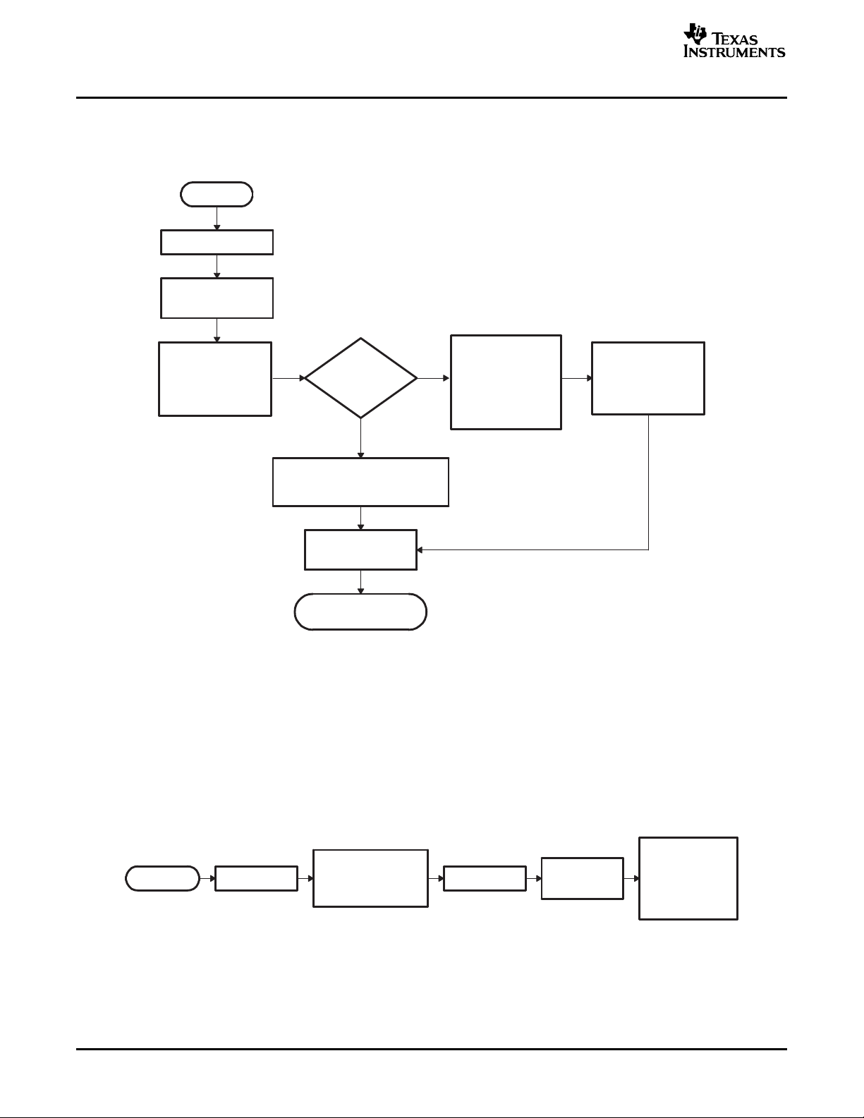
2.1 Bootloader Functional Operation
The bootloader is the program located in the on-chip boot ROM that is executed following a reset.
The bootloader is used to transfer code from an external source into internal memory following power up.
This allows code to reside in slow non-volatile memory externally, and be transferred to high-speed
memory to be executed.
The bootloader provides a variety of different ways to download code to accommodate different system
requirements. The bootloader uses various GPIO signals to determine which boot mode to use. The boot
mode selection process as well as the specifics of each bootloader are described in the remainder of this
document. Figure 2-1 shows the basic bootloader flow.
Figure 2-1. Bootloader Flow Diagram
The reset vector in boot ROM redirects program execution to the InitBoot function. After performing device
initialization the bootloader will check the state of GPIO pins to determine which boot mode you want to
execute. Options include: jump to flash, jump to SARAM, jump to OTP, or call one of the on-chip boot
loading routines.
After the selection process and if the required boot loading is complete, the processor will continue
execution at an entry point determined by the boot mode selected. If a bootloader was called, then the
input stream loaded by the peripheral determines this entry address. This data stream is described in
Section 2.10 . If, instead, you choose to boot directly to flash, OTP, or SARAM, the entry address is
predefined for each of these memory blocks.
The following sections discuss in detail the different boot modes available and the process used for
loading data code into the device.
Bootloader Features18 SPRU722C – November 2004 – Revised October 2006
Submit Documentation Feedback
Page 19

www.ti.com
2.2 Bootloader Device Configuration
At reset, any 28x™ CPU-based device is in 27x™ object-compatible mode. It is up to the application to
place the device in the proper operating mode before execution proceeds.
On the 28x devices, when booting from the internal boot ROM, the device is configured for 28x operating
mode by the boot ROM software. You are responsible for any additional configuration required.
For example, if your application includes C2xLP™ source, then you are responsible for configuring the
device for C2xLP source compatibility prior to execution of code generated from C2xLP source.
The configuration required for each operating mode is summarized in Table 2-1 .
Bootloader Device Configuration
Table 2-1. Configuration for Device Modes
C27x Mode (Reset) 28x Mode Compatible Mode
OBJMODE 0 1 1
AMODE 0 0 1
PAGE0 0 0 0
M0M1MAP
Other Settings SXM = 1, C = 1, SPM = 0
(1)
(1)
Normally for C27x compatibility, the M0M1MAP would be 0. On these devices, however, it is tied off
high internally; therefore, at reset, M0M1MAP is always configured for 28x mode.
1 1 1
C2xLP Source
2.3 PLL Multiplier Selection
The boot ROM does not change the state of the PLL. Note that the PLL multiplier is not affected by a
reset from the debugger. Therefore, a boot that is initialized from a reset from Code Composer Studio™
may be at a different speed than booting by pulling the external reset line ( XRS) low.
2.4 Watchdog Module
When branching directly to flash, M0 single-access RAM (SARAM), or one-time-programmable (OTP)
memory, the watchdog is not touched. In the other boot modes, the watchdog is disabled before booting
and then re-enabled and cleared before branching to the final destination address.
SPRU722C – November 2004 – Revised October 2006 Bootloader Features 19
Submit Documentation Feedback
Page 20

www.ti.com
Taking an ITRAP Interrupt
2.5 Taking an ITRAP Interrupt
If an illegal opcode is fetched, the 28x will take an ITRAP (illegal trap) interrupt. During the boot process,
the interrupt vector used by the ITRAP is within the CPU vector table of the boot ROM. As of version 4 of
the boot ROM code, the ITRAP vector points to an interrupt service routine (ISR) within the boot ROM
named ITRAPIsr(). This interrupt service routine attempts to enable the watchdog and then loops forever
until the processor is reset. This ISR will be used for any ITRAP until the user's application initializes and
enables the peripheral interrupt expansion (PIE) block. Once the PIE is enabled, the ITRAP vector located
within the PIE vector table will be used. Prior to boot ROM code version 4, the ITRAP interrupt vector in
the CPU vector table pointed to a RAM location in M0 memory. Refer to Section 4.1 to determine the boot
ROM code version of a particular device.
2.6 Internal Pullup Resisters
Each GPIO pin has an internal pullup resistor that can be enabled or disabled in software. The pins that
are read by the boot mode selection code to determine the boot mode selection have pull-ups enabled
after reset by default. In noisy conditions it is still recommended that you configure each of the three boot
mode selection pins externally.
The individual bootloaders SCI, SPI, eCAN, and parallel boot all enable the pullup resistors for the pins
that are used for control and data transfer. The bootloader leaves the resistors enabled for these pins
when it exits. For example, the SCI-A bootloader enables the pullup resistors on the SCITXA and SCIRXA
pins. It is your responsibility to disable them, if desired, after the bootloader exits.
2.7 PIE Configuration
The boot modes do not enable the PIE. It is left in its default state, which is disabled.
2.8 Reserved Memory
The first 80 words of the M1 memory block (address 0x400 - 0x44F) are reserved for the stack and .ebss
code sections during the boot-load process. If code is bootloaded into this region there is no error
checking to prevent it from corrupting the boot ROM stack.
Bootloader Features20 SPRU722C – November 2004 – Revised October 2006
Submit Documentation Feedback
Page 21

www.ti.com
2.9 Bootloader Modes
To accommodate different system requirements, the boot ROM offers a variety of different boot modes.
This section describes the different boot modes and gives brief summary of their functional operation. The
states of three GPIO pins are used to determine the desired boot mode as shown in Table 2-2 .
Boot to Flash
SCI-A Boot Load a data stream from SCI-A. 1 1 0
SPI-A Boot Load from an external serial SPI EEPROM on SPI-A. 1 0 1
I2C Boot Load data from an external EEPROM at address 0x50 on the 1 0 0
eCAN-A Boot
Boot to M0 SARAM
Boot to OTP
Parallel I/O Boot Load data from GPIO0 - GPIO15. 0 0 0
(1)
You must take extra care because of any effect toggling SPICLKA to select a boot mode may have on external logic.
(2)
When booting directly to flash, it is assumed that you have previously programmed a branch statement at 0x3F 7FF6 to redirect
program flow as desired.
(3)
On devices that do not have an eCAN-A module this configuration is reserved. If it is selected, then the eCAN-A bootloader will
run and will loop forever waiting for an incoming message.
(4)
When booting directly to OTP or M0 SARAM, it is assumed that you have previously programmed or loaded code starting at the
entry point location.
Bootloader Modes
Table 2-2. Boot Mode Selection
Mode Description GPIO18 GPIO29 GPIO34
SPICLKA
SCITXDB
(2)
Jump to flash address 0x3F 7FF6. You must have programmed 1 1 1
a branch instruction here prior to reset to redirect code
execution as desired.
I2C bus.
(3)
(4)
Call CAN_Boot to load from eCAN-A mailbox 1. 0 1 1
(4)
Jump to M0 SARAM address 0x00 0000. 0 1 0
Jump to OTP address 0x3D 7800. 0 0 1
(1)
SCITXDA
SPRU722C – November 2004 – Revised October 2006 Bootloader Features 21
Submit Documentation Feedback
Page 22
www.ti.com
Reset
InitBoot
Call
SelectBootMode
Read the state
of I/O pins to
determine what
boot mode is
desired
Call
Boot Loader
?
No
Yes
EntryPoint determined
directly from state of
I/O pins
Call
boot loader,
SCI, SPI,
I2C, eCAN, or
parallel I/O
EntryPoint
and load
data/code
Read
Call
ExitBoot
Begin execution
at EntryPoint
Reset InitBoot
SelectBootMode
Select jump
to flash
ExitBoot
Jump to
0x3F 7FF6
User
programmed
branch to
desired
location
Bootloader Modes
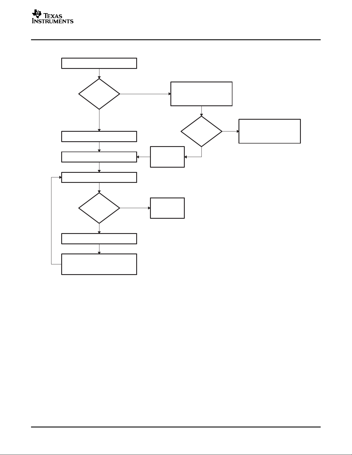
Figure 2-2 shows an overview of the boot process. Each step is described in greater detail in following
sections.
Figure 2-2. Boot ROM Function Overview
The following boot modes do not call a bootloader. Instead, they jump to a predefined location in memory:
• Jump to branch instruction in flash memory
• Jump to M0 SARAM
22 Bootloader Features SPRU722C – November 2004 – Revised October 2006
In this mode, the boot ROM software will configure the device for 28x operation and then branch
directly to location 0x3F 7FF6 in flash memory. This location is just before the 128-bit code security
module (CSM) password locations. You are required to have previously programmed a branch
instruction at location 0x3F 7FF6 that will redirect code execution to either a custom boot-loader or the
application code.
On RAM-only devices, the boot-to-flash option jumps to reserved memory and should not be used. On
ROM-only devices, the boot-to-flash option jumps to the location 0x3F7FF6 in ROM.
Figure 2-3. Jump-to-Flash Flow Diagram
In this mode, the boot ROM software will configure the device for 28x operation and then branch
directly to 0x00 0000; the first address in the M0 SARAM memory block
Submit Documentation Feedback
Page 23
www.ti.com
Reset InitBoot
SelectBootMode
Select jump
to M0 SARAM
ExitBoot
Jump to
0x00 0000
Execution
continues
Reset InitBoot
SelectBootMode
Select jump
to OTP
ExitBoot
Jump to
0x3D 7800
Execute
preprogrammed
OTP code
Bootloader Modes
Figure 2-4. Flow Diagram of Jump to M0 SARAM
• Jump to OTP memory
In this mode, the boot ROM software will configure the device for 28x operation and then branch
directly to at 0x3D 7800; the first address in the OTP memory block.
On ROM devices, the boot-to-OTP option jumps to address 0x3D 7800 in ROM. On RAM devices, the
boot-to-OTP option jumps to reserved memory and should not be used.
Figure 2-5. Flow Diagram of Jump-to-OTP Memory
The following boot modes call a boot load routine that loads a data stream from the peripheral into
memory:
• Standard serial boot mode (SCI-A)
In this mode, the boot ROM will load code to be executed into on-chip memory via the SCI-A port.
• SPI EEPROM boot mode (SPI-A)
In this mode, the boot ROM will load code and data into on-chip memory from an external EEPROM
via the SPI-A port.
• I2C-A boot mode (I2C-A)
In this mode, the boot ROM will load code and data into on-chip memory from an external EEPROM at
address 0x50 on the I2C-A bus. The EEPROM must adhere to conventional I2C EEPROM protocol with
a 16-bit base address architecture.
• eCAN Boot Mode (eCAN-A)
In this mode, the eCAN-A peripheral is used to transfer data and code into the on-chip memory using
eCAN-A mailbox 1. The transfer is an 8-bit data stream with two 8-bit values being transferred during
each communication. On devices that do not have an eCAN-A peripheral, this mode is reserved and
should not be used.
• Boot from GPIO Port (Parallel Boot from GPIO0-GPIO15)
In this mode, the boot ROM uses GPIO port A pins GPIO0-GPIO15 to load code and data from an
external source. This mode supports both 8-bit and 16-bit data streams. Since this mode requires a
number of GPIO pins, it is typically used to download code for flash programming when the device is
connected to a platform explicitly for flash programming and not a target board.
SPRU722C – November 2004 – Revised October 2006 Bootloader Features 23
Submit Documentation Feedback
Page 24

www.ti.com
Bootloader Data Stream Structure
2.10 Bootloader Data Stream Structure
The following two tables and associated examples show the structure of the data stream incoming to the
bootloader. The basic structure is the same for all the bootloaders and is based on the C54x source data
stream generated by the C54x hex utility. The C28x hex utility (hex2000.exe) has been updated to support
this structure. The hex2000.exe utility is included with the C2000 code generation tools. All values in the
data stream structure are in hex.
The first 16-bit word in the data stream is known as the key value. The key value is used to tell the
bootloader the width of the incoming stream: 8 or 16 bits. Note that not all bootloaders will accept both 8
and 16-bit streams. Please refer to the detailed information on each loader for the valid data stream width.
For an 8-bit data stream, the key value is 0x08AA and for a 16-bit stream it is 0x10AA. If a bootloader
receives an invalid key value, then the load is aborted. In this case, the entry point for the flash memory
(0x3F 7FF6) will be used.
The next 8 words are used to initialize register values or otherwise enhance the bootloader by passing
values to it. If a bootloader does not use these values then they are reserved for future use and the
bootloader simply reads the value and then discards it. Currently only the SPI and I2C bootloaders use
these words to initialize registers.
The tenth and eleventh words comprise the 22-bit entry point address. This address is used to initialize
the PC after the boot load is complete. This address is most likely the entry point of the program
downloaded by the bootloader.
The twelfth word in the data stream is the size of the first data block to be transferred. The size of the
block is defined for both 8-bit and 16-bit data stream formats as the number of 16-bit words in the block.
For example, to transfer a block of 20 8-bit data values from an 8-bit data stream, the block size would be
0x000A to indicate 10 16-bit words.
The next two words tell the loader the destination address of the block of data. Following the size and
address will be the 16-bit words that makeup that block of data.
This pattern of block size/destination address repeats for each block of data to be transferred. Once all the
blocks have been transferred, a block size of 0x0000 signals to the loader that the transfer is complete. At
this point the loader will return the entry point address to the calling routine which in turn will cleanup and
exit. Execution will then continue at the entry point address as determined by the input data stream
contents.
Bootloader Features24 SPRU722C – November 2004 – Revised October 2006
Submit Documentation Feedback
Page 25

www.ti.com
Bootloader Data Stream Structure
Table 2-3. General Structure Of Source Program Data Stream In 16-Bit Mode
Word Contents
1 10AA (KeyValue for memory width = 16bits)
2 Register initialization value or reserved for future use
3 Register initialization value or reserved for future use
4 Register initialization value or reserved for future use
5 Register initialization value or reserved for future use
6 Register initialization value or reserved for future use
7 Register initialization value or reserved for future use
8 Register initialization value or reserved for future use
9 Register initialization value or reserved for future use
10 Entry point PC[22:16]
11 Entry point PC[15:0]
12 Block size (number of words) of the first block of data to load. If the block size is 0, this indicates the end
13 Destination address of first block Addr[31:16]
14 Destination address of first block Addr[15:0]
15 First word of the first block in the source being loaded
... ...
... ...
. Last word of the first block of the source being loaded
. Block size of the 2nd block to load.
. Destination address of second block Addr[31:16]
. Destination address of second block Addr[15:0]
. First word of the second block in the source being loaded
. …
. Last word of the second block of the source being loaded
. Block size of the last block to load
. Destination address of last block Addr[31:16]
. Destination address of last block Addr[15:0]
. First word of the last block in the source being loaded
... ...
... ...
n Last word of the last block of the source being loaded
n+1 Block size of 0000h - indicates end of the source program
of the source program. Otherwise another section follows.
SPRU722C – November 2004 – Revised October 2006 Bootloader Features 25
Submit Documentation Feedback
Page 26

www.ti.com
Bootloader Data Stream Structure
Example 2-1. Data Stream Structure 16-bit
10AA ; 0x10AA 16-bit key value
0000 ; 8 reserved words
0000
0000
0000
0000
0000
0000
0000
003F ; 0x003F8000 EntryAddr, starting point after boot load completes
8000
0005 ; 0x0005 - First block consists of 5 16-bit words
003F ; 0x003F9010 - First block will be loaded starting at 0x3F9010
9010
0001 ; Data loaded = 0x0001 0x0002 0x0003 0x0004 0x0005
0002
0003
0004
0005
0002 ; 0x0002 - 2nd block consists of 2 16-bit words
003F ; 0x003F8000 - 2nd block will be loaded starting at 0x3F8000
8000
7700 ; Data loaded = 0x7700 0x7625
7625
0000 ; 0x0000 - Size of 0 indicates end of data stream
After load has completed the following memory values will have been initialized as follows:
Location Value
0x3F9010 0x0001
0x3F9011 0x0002
0x3F9012 0x0003
0x3F9013 0x0004
0x3F9014 0x0005
0x3F8000 0x7700
0x3F8001 0x7625
PC Begins execution at 0x3F8000
26 Bootloader Features SPRU722C – November 2004 – Revised October 2006
Submit Documentation Feedback
Page 27

www.ti.com
Bootloader Data Stream Structure
In 8-bit mode, the least significant byte (LSB) of the word is sent first followed by the most significant byte
(MSB). For 32-bit values, such as a destination address, the most significant word (MSW) is loaded first,
followed by the least significant word (LSW). The bootloaders take this into account when loading an 8-bit
data stream.
Table 2-4. LSB/MSB Loading Sequence in 8-Bit Data Stream
Byte Contents
LSB (First Byte of 2) MSB (Second Byte of 2)
1 2 LSB: AA (KeyValue for memory width = 8 bits) MSB: 08h (KeyValue for memory width = 8 bits)
3 4 LSB: Register initialization value or reserved MSB: Register initialization value or reserved
5 6 LSB: Register initialization value or reserved MSB: Register initialization value or reserved
7 8 LSB: Register initialization value or reserved MSB: Register initialization value or reserved
... ... ... ...
... ... ... ...
17 18 LSB: Register initialization value or reserved MSB: Register initialization value or reserved
19 20 LSB: Upper half of Entry point PC[23:16] MSB: Upper half of entry point PC[31:24] (Always 0x00)
21 22 LSB: Lower half of Entry point PC[7:0] MSB: Lower half of Entry point PC[15:8]
23 24 LSB: Block size in words of the first block to load. If the MSB: block size
25 26 LSB: MSW destination address, first block Addr[23:16] MSB: MSW destination address, first block Addr[31:24]
27 28 LSB: LSW destination address, first block Addr[7:0] MSB: LSW destination address, first block Addr[15:8]
29 30 LSB: First word of the first block being loaded MSB: First word of the first block being loaded
... ... ... ...
... ... ... ...
. . LSB: Last word of the first block to load MSB: Last word of the first block to load
. . LSB: Block size of the second block MSB: Block size of the second block
. . LSB: MSW destination address, second block Addr[23:16] MSB: MSW destination address, second block
. . LSB: LSW destination address, second block Addr[7:0] MSB: LSW destination address, second block Addr[15:8]
. . LSB: First word of the second block being loaded MSB: First word of the second block being loaded
... ... ... ...
... ... ... ...
. . LSB: Last word of the second block MSB: Last word of the second block
. . LSB: Block size of the last block MSB: Block size of the last block
. . LSB: MSW of destination address of last block Addr[23:16] MSB: MSW destination address, last block Addr[31:24]
. . LSB: LSW destination address, last block Addr[7:0] MSB: LSW destination address, last block Addr[15:8]
. . LSB: First word of the last block being loaded MSB: First word of the last block being loaded
... ... ... ...
... ... ... ...
. . LSB: Last word of the last block MSB: Last word of the last block
n n+1 LSB: 00h MSB: 00h - indicates the end of the source
block size is 0, this indicates the end of the source
program. Otherwise another block follows. For example, a
block size of 0x000A would indicate 10 words or 20 bytes
in the block.
Addr[31:24]
SPRU722C – November 2004 – Revised October 2006 Bootloader Features 27
Submit Documentation Feedback
Page 28

www.ti.com
Basic Transfer Procedure
Example 2-2. Data Stream Structure 8-bit
AA 08 ; 0x08AA 8-bit key value
00 00 00 00 ; 8 reserved words
00 00 00 00
00 00 00 00
00 00 00 00
3F 00 00 80 ; 0x003F8000 EntryAddr, starting point after boot load completes
05 00 ; 0x0005 - First block consists of 5 16-bit words
3F 00 10 90 ; 0x003F9010 - First block will be loaded starting at 0x3F9010
01 00 ; Data loaded = 0x0001 0x0002 0x0003 0x0004 0x0005
02 00
03 00
04 00
05 00
02 00 ; 0x0002 - 2nd block consists of 2 16-bit words
3F 00 00 80 ; 0x003F8000 - 2nd block will be loaded starting at 0x3F8000
00 77 ; Data loaded = 0x7700 0x7625
25 76
00 00 ; 0x0000 - Size of 0 indicates end of data stream
After load has completed the following memory values will have been initialized as follows:
Location Value
0x3F9010 0x0001
0x3F9011 0x0002
0x3F9012 0x0003
0x3F9013 0x0004
0x3F9014 0x0005
0x3F8000 0x7700
0x3F8001 0x7625
PC Begins execution at 0x3F8000
2.11 Basic Transfer Procedure
Figure 2-6 illustrates the basic process a bootloader uses to determine whether 8-bit or 16-bit data stream
has been selected, transfer that data, and start program execution. This process occurs after the
bootloader finds the valid boot mode selected by the state of GPIO pins.
The loader first compares the first value sent by the host against the 16-bit key value of 0x10AA. If the
value fetched does not match then the loader will read a second value. This value will be combined with
the first value to form a word. This will then be checked against the 8-bit key value of 0x08AA. If the
loader finds that the header does not match either the 8-bit or 16-bit key value, or if the value is not valid
for the given boot mode then the load will abort. In this case the loader will return the entry point address
for the flash to the calling routine.
28 Bootloader Features SPRU722C – November 2004 – Revised October 2006
Submit Documentation Feedback
Page 29
www.ti.com
Read first word (W1)
W1=
0x10AA
?
No
16-bit data size
Yes
Read EntryPoint address
Read second word
(W2) and discard
upper 8-bits
?
0x08AA
W2:W1=
Yes
No
8-bit
DataSize
Data format error
Return
FLASH_ENTRY_POINT
Read BlockSize (R)
?
R=0
No
Yes
Return
EntryPoint
Read BlockAddress
Transfer R words of
data from source to
destination
Figure 2-6. Bootloader Basic Transfer Procedure
InitBoot Assembly Routine
A 8-bit and 16-bit transfers are not valid for all boot modes. See the info specific to a particular bootloader for any
limitations.
B In 8-bit mode, the LSB of the 16-bit word is read first followed by the MSB.
2.12 InitBoot Assembly Routine
The first routine called after reset is the InitBoot assembly routine. This routine initializes the device for
operation in C28x object mode. InitBoot also performs a dummy read of the Code Security Module (CSM)
password locations. If the CSM passwords are erased (all 0xFFFFs) then this has the effect of unlocking
the CSM. Otherwise the CSM will remain locked and this dummy read of the password locations will have
no effect. This can be useful if you have a new device that you want to boot load.
After the dummy read of the CSM password locations, the InitBoot routine calls the SelectBootMode
function. This function determines the type of boot mode desired by the state of certain GPIO pins. This
process is described in Section 2.13 . Once the boot is complete, the SelectBootMode function passes
back the entry point address (EntryAddr) to the InitBoot function. EntryAddr is the location where code
execution will begin after the bootloader exits. InitBoot then calls the ExitBoot routine that then restores
CPU registers to their reset state and exits to the EntryAddr that was determined by the boot mode.
SPRU722C – November 2004 – Revised October 2006 Bootloader Features 29
Submit Documentation Feedback
Page 30

www.ti.com
Init Boot
Initialize device
OBJMODE=1
AMODE = 0
MOM1MAP=1
DP = 0
OVM = 0
SPM= 0
SP = 0x400
Dummy read of
CSM password
locations
Call
SelectBootMode
Call
ExitBoot
SelectBootMode Function
2.13 SelectBootMode Function
To determine the desired boot mode, the SelectBootMode function examines the state of 3 GPIO pins as
shown in Table 2-5 .
Mode Description GPIO18 GPIO29 GPIO34
Boot to Flash
SCI-A Boot Load from SCI-A. 1 1 0
SPI-A Boot Load from an external serial SPI EEPROM on SPI-A. 1 0 1
I2C-A Boot Load from an external EEPROM at address 0x50 on the 1 0 0
eCAN-A Boot
Boot to M0 SARAM
Boot to OTP
Parallel I/O Boot Load from GPIO0 - GPIO15. 0 0 0
Figure 2-7. Overview of InitBoot Assembly Function
Table 2-5. Boot Mode Selection
SPICLKA
(2)
(3)
(4)
Jump to flash address 0x3F 7FF6. You must have 1 1 1
programmed a branch instruction here prior to reset to
redirect code execution as desired.
I2C-A bus.
Call CAN_Boot to load from eCAN-A mailbox 1. 0 1 1
(4)
Jump to M0 SARAM address 0x00 0000. 0 1 0
Jump to OTP address 0x3D 7800. 0 0 1
(1)
SCITXB
SCITXA
30 Bootloader Features SPRU722C – November 2004 – Revised October 2006
(1)
You must take extra care because of any effect toggling SPICLKA to select a boot mode may have on external logic.
(2)
When booting directly to flash, it is assumed that you have previously programmed a branch statement at 0x3F 7FF6 to redirect
program flow as desired.
(3)
On devices without an eCAN-A module, this mode is reserved and should not be used.
(4)
When booting directly to OTP or MO, it is assumed that you have previously programmed or loaded code starting at the entry
point location.
For a boot mode to be selected, the pins corresponding to the desired boot mode have to be pulled low or
high until the selection process completes. Note that the state of the selection pins is not latched at reset;
they are sampled some cycles later in the SelectBootMode function. The internal pullup resistors are
enabled at reset for the boot mode selection pins. It is still suggested that the boot mode configuration be
made externally to avoid the effect of any noise on these pins.
The SelectBootMode function checks the missing clock detect bit (MCLKSTS) in the PLLSTS register to
determine if the PLL is operating in limp mode. If the PLL is operating in limp mode, the boot mode select
function takes an appropriate action depending on the boot mode selected:
• Boot to flash, OTP, SARAM, I2C-A, SPI-A and the parallel I/O
These modes behave as normal. The user's software must check for missing clock status and take the
appropriate action if the MCLKSTS bit is set.
Submit Documentation Feedback
Page 31

www.ti.com
SelectBootMode Function
• SCI-A boot
The SCI bootloader will be called. Depending on the requested baud rate, however, the device may
not be able to autobaud lock. In this case the boot ROM software will loop in the autobaud lock
function indefinitely. Should the SCI-A boot complete, the user's software must check for a missing
clock status and take the appropriate action.
• eCAN-A boot
The eCAN bootloader will not be called. Instead the boot ROM will loop indefinitely.
Note: The SelectBootMode routine disables the watchdog before calling the SCI, I2C, eCAN,
SPI or parallel bootloader. The bootloaders do not service the watchdog and assume that
it is disabled. Before exiting, the SelectBootMode routine will re-enable the watchdog and
reset its timer.
If a bootloader is not going to be called, then the watchdog is left untouched.
When selecting a boot mode, the pins should be pulled high or low through a weak pulldown or weak
pull-up such that the DSP can drive them to a new state when required. For example, if you wanted to
boot from the SCI-A one of the pins you pull high is the SCITXDA pin. This pullup must be weak so that
when the SCI boot process begins the DSP will be able to properly transmit through the TX pin. Likewise
for the remaining boot mode selection pins.
You must take extra care using the SPICLKA signal to select a boot mode. Toggling of this signal may
affect external logic and this effect must be taken into account.
SPRU722C – November 2004 – Revised October 2006 Bootloader Features 31
Submit Documentation Feedback
Page 32

www.ti.com
SelectBootMode
Configure GPIO18, GPIO29,
GPIO34 as input pins
Read boot mode
pins
Dummy read of
CSM password
FLASH
boot
?
Return
FLASH_ENTRY_POINT
EntryAddr: 0x3F 7FF6
Yes
No
boot
?
M0
Return
M0_ENTRY_POINT
EntryAddr: 0x00 0000
OTP
boot
?
Return
OTP_ENTRY_POINT
EntryAddr: 0x3D 7800
WatchDogDisable
Call
SCI
boot
?
Call
SCI_Boot
?
SPI
boot
SPI_Boot
Call
?
eCAN
boot
?
I2C
boot
Call
eCAN_Boot
I2C_Boot
Call
Parallel_Boot
Call
WatchDogEnable
Call
Return EntryAddr as
determined by boot
loader called.
This location is just before the
CSM password.
Direct branch to the
M0 SARAM block
Execute user custom boot
loader or TI-provided boot loader
memory without using up main
flash memory.
Bootloader selected (SCI, SPI or
parallel) will copy data from the
external device to internal memory.
A section of the data read determines
the EntryPoint for execution after the
boot routines have completed.
Yes
Yes
Yes
Yes
Yes
Yes
No
No
No
No
No
No
You must have previously programmed
a branch statement at flash address
0x3F 7FF6 to redirect program as
desired.
SelectBootMode Function
Figure 2-8. Overview of the SelectBootMode Function
Bootloader Features32 SPRU722C – November 2004 – Revised October 2006
Submit Documentation Feedback
Page 33

www.ti.com
2.14 CopyData Function
CopyData
Call peripheral-specific
GetWordData to read
Yes
No
Return
BlockHeader.BlockSize
BlockSize=
0x0000
?
Call GetLongData
to read
BlockHeader.DestAddr
Transfer
BlockHeader.BlockSize
words of data from
port to memory
starting at DestAddr
DSP
SCIRXDA
SCITXDA
Host
(Data and program
source)
Each of the bootloaders uses the same function to copy data from the port to the DSP SARAM. This
function is the CopyData() function. This function uses a pointer to a GetWordData function that is
initialized by each of the loaders to properly read data from that port. For example, when the SPI loader is
evoked, the GetWordData function pointer is initialized to point to the SPI-specific SPI_GetWordData
function. Thus when the CopyData() function is called, the correct port is accessed. The flow of the
CopyData function is shown in Figure 2-9 .
CopyData Function
Figure 2-9. Overview of CopyData Function
2.15 SCI_Boot Function
SPRU722C – November 2004 – Revised October 2006 Bootloader Features 33
Submit Documentation Feedback
The SCI boot mode asynchronously transfers code from SCI-A to internal memory. This boot mode only
supports an incoming 8-bit data stream and follows the same data flow as outlined in Example 2-2 .
Figure 2-10. Overview of SCI Bootloader Operation
The DSP communicates with the external host device by communication through the SCI-A Peripheral.
The autobaud feature of the SCI port is used to lock baud rates with the host. For this reason the SCI
loader is very flexible and you can use a number of different baud rates to communicate with the DSP.
After each data transfer, the DSP will echo back the 8-bit character received to the host. In this manner,
the host can perform checks that each character was received by the DSP.
Page 34

www.ti.com
SCI_Boot
Enable the SCI-A clock
set the LSPCLK to /4
functionality and pullups on
Enable the SCIA TX and RX pin
Setup SCI-A for
1 stop, 8-bit character,
no parity, use internal
SC clock, no loopback,
disable Rx/Tx interrupts
Disable SCI FIFOs
Prime SCI-A baud register
Enable autobaud detection
Autobaud
lock
?
No
Yes
Echo autobaud character
Read KeyValue
Yes
No
Valid
KeyValue
(0x08AA)
?
Return
FLASH_ENTRY_POINT
Read and discard 8
reserved words
Read EntryPoint address
Call CopyData
EntryPoint
Return
Set GetWord function pointer
to SCIA_GetWordData
TX and RX
SCI_Boot Function
At higher baud rates, the slew rate of the incoming data bits can be effected by transceiver and connector
performance. While normal serial communications may work well, this slew rate may limit reliable
auto-baud detection at higher baud rates (typically beyond 100kbaud) and cause the auto-baud lock
feature to fail. To avoid this, the following is recommended:
1. Achieve a baud-lock between the host and 28x SCI bootloader using a lower baud rate.
2. Load the incoming 28x application or custom loader at this lower baud rate.
3. The host may then handshake with the loaded 28x application to set the SCI baud rate register to the
desired high baud rate.
Figure 2-11. Overview of SCI_Boot Function
34 Bootloader Features SPRU722C – November 2004 – Revised October 2006
Submit Documentation Feedback
Page 35

www.ti.com
SCIA_GetWordData
Yes
NoData
Received
?
Echoback LSB
to host
Read LSB
Data
Received
?
No
Yes
Read MSB
Echoback MSB
to host
Return MSB:LSB
DSP
DSP control − GPIO26
Host control − GPIO27
Host
(Data and program
source)
Data GP I/O port GPIO[15:0]
16
Figure 2-12. Overview of SCI_GetWordData Function
Parallel_Boot Function (GPIO)
2.16 Parallel_Boot Function (GPIO)
The parallel general purpose I/O (GPIO) boot mode asynchronously transfers code from GPIO0-GPIO15
to internal memory. Each value can be 16 bits or 8 bits long and follows the same data flow as outlined
inData Stream Structure.
Figure 2-13. Overview of Parallel GPIO bootloader Operation
The 28x communicates with the external host device by polling/driving the GPIO27 and GPIO26 lines. The
handshake protocol shown in Figure 2-14 must be used to successfully transfer each word via
GPIO[15:0]. This protocol is very robust and allows for a slower or faster host to communicate with the
DSP.
If the 8-bit mode is selected, two consecutive 8-bit words are read to form a single 16-bit word. The most
significant byte (MSB) is read first followed by the least significant byte (LSB). In this case, data is read
from the lower eight lines of GPIO[7:0] ignoring the higher byte.
The DSP first signals the host that the DSP is ready to begin data transfer by pulling the GPIO26 pin low.
The host load then initiates the data transfer by pulling the GPIO27 pin low. The complete protocol is
shown in the diagram below:
SPRU722C – November 2004 – Revised October 2006 Bootloader Features 35
Submit Documentation Feedback
Page 36

www.ti.com
Host control
GPIO27
DSP control
GPIO26
1 2 3 4 65
Parallel_Boot
No
Yes
Initialize GP I/O MUX
and Dir registers
GPIO[15:0] = input
GPIO27 = input
GPIO26=output
Read KeyValue to
determine DataSize
Valid
KeyValue
(0x08AA or
0x10AA)
?
reserved words
Read and discard 8
Read EntryPoint
address
CopyData
Call
Return
EntryPoint
Return
FLASH_ENTRY_POINT
Enable pullups on
GPIO[15:0], GPIO26,
and GPIO27
and assign appropriate
GetWordData function
Parallel_Boot Function (GPIO)
1. The DSP indicates it is ready to start receiving data by pulling the GPIO26 pin low.
2. The bootloader waits until the host puts data on GPIO[15:0]. The host signals to the DSP that data is
ready by pulling the GPIO27 pin low.
3. The DSP reads the data and signals the host that the read is complete by pulling GPIO26 high.
4. The bootloader waits until the host acknowledges the DSP by pulling GPIO27 high.
5. The DSP again indicates it is ready for more data by pulling the GPIO26 pin low.
This process is repeated for each data value to be sent.
Figure 2-15 shows an overview of the Parallel GPIO bootloader flow.
Figure 2-14. Parallel GPIO bootloader Handshake Protocol
Figure 2-15. Parallel GPIO Mode Overview
36 Bootloader Features SPRU722C – November 2004 – Revised October 2006
Figure 2-16 shows the transfer flow from the host side. The operating speed of the CPU and host are not
critical in this mode as the host will wait for the DSP and the DSP will in turn wait for the host. In this
manner the protocol will work with both a host running faster and a host running slower then the DSP.
Submit Documentation Feedback
Page 37

www.ti.com
Start transfer
No
More
data
?
DSP ready
(GPIO26=0)
?
Yes
Load GPIO[15:0] with data
Signal that data
is ready
(GPIO27=0)
DSP ack
(GPIO26=1)
?
No
Yes
Acknowledge DSP
(GPIO27=1)
Yes
No
End transfer
Figure 2-16. Parallel GPIO Mode - Host Transfer Flow
Parallel_Boot Function (GPIO)
Figure 2-17 and Figure 2-18 show the flow used to read a single word of data from the parallel port. The
loader uses the method shown in Figure 2-6 to read the key value and to determine if the incoming data
stream width is 8-bit or 16-bit. A different GetWordData function is used by the parallel loader depending
on the data size of the incoming data stream.
• 16-bit data stream
For an 16-bit data stream, the function Parallel_GetWordData16bit is used. This function reads all
16-bits at a time. The flow of this function is shown in Figure 2-17 .
• 8-bit data stream
For an 8-bit data stream, the function Parallel_GetWordData8bit is used. The 8-bit routine, shown in
Figure 2-18 , discards the upper 8 bits of the first read from the port and treats the lower 8 bits as the
least significant byte (LSB) of the word to be fetched. The routine will then perform a second read to
fetch the most significant byte (MSB). It then combines the MSB and LSB into a single 16-bit value to
be passed back to the calling routine.
SPRU722C – November 2004 – Revised October 2006 Bootloader Features 37
Submit Documentation Feedback
Page 38

www.ti.com
(GPIO26 = 0)
Signal host that DSP is ready
Parallel_GetWordData16bit
Data
ready
(GPIO27 = 0)
?
No
Yes
GPIO[15:0]
Read word of data from
(GPIO26 = 1)
DSP ack read complete
Host
ack
(GPIO27 = 1)
?
Yes
No
Return WordData
Parallel_Boot Function (GPIO)
Figure 2-17. 16-Bit Parallel GetWord Function
38 Bootloader Features SPRU722C – November 2004 – Revised October 2006
Submit Documentation Feedback
Page 39

www.ti.com
(GPIO26 = 0)
Signal host that DSP is ready
Parallel_GetWordData
8 bit
(GPIO27 = 0)
?
Data
ready
Yes
from GPIO 15:0
Read word of data
(GPIO26 = 1)
DSP ack read complete
(GPIO27 = 1)
ack
Host
No
?
A
ack
Host
(GPIO27 = 1)
DSP ack read complete
(GPIO26 = 1)
?
ready
Data
(GPIO27 = 0)
Signal host that DSP
(GPIO26 = 0)
is ready to read MSB
?
A
Read word from
GPIO[15:0], discard
the upper 8 bits, MSB
of data = lower 8 bits
Return WordData
WordData = MSB:LSB
No
No
No
Yes
Yes
Yes
Figure 2-18. 8-Bit Parallel GetWord Function
Parallel_Boot Function (GPIO)
SPRU722C – November 2004 – Revised October 2006 Bootloader Features 39
Submit Documentation Feedback
Page 40

www.ti.com
SPISIMOA
SPISOMIA
SPICLKA
SPIESTEA
DIN
DOUT
CLK
CS
DSP
Serial SPI
EEPROM
SPI_Boot Function
2.17 SPI_Boot Function
The SPI loader expects an 8-bit wide SPI-compatible serial EEPROM device to be present on the SPI-A
pins as indicated in Figure 2-19 . The SPI bootloader does not support a 16-bit data stream.
Figure 2-19. SPI Loader
The SPI boot ROM loader initializes the SPI module to interface to a serial SPI EEPROM. Devices of this
type include, but are not limited to, the Xicor X25320 (4Kx8) and Xicor X25256 (32Kx8) SPI serial SPI
EEPROMs.
The SPI boot ROM loader initializes the SPI with the following settings: FIFO enabled, 8-bit character,
internal SPICLK master mode and talk mode, clock phase = 0, polarity = 0, using the slowest baud rate.
If the download is to be performed from an SPI port on another device, then that device must be setup to
operate in the slave mode and mimic a serial SPI EEPROM. Immediately after entering the SPI_Boot
function, the pin functions for the SPI pins are set to primary and the SPI is initialized. The initialization is
done at the slowest speed possible. Once the SPI is initialized and the key value read, you could specify a
change in baud rate or low speed peripheral clock.
Table 2-6. SPI 8-Bit Data Stream
Byte Contents
1 LSB: AA (KeyValue for memory width = 8-bits)
2 MSB: 08h (KeyValue for memory width = 8-bits)
3 LSB: LOSPCP
4 MSB: SPIBRR
5 LSB: reserved for future use
6 MSB: reserved for future use
... ...
... ...
17 LSB: reserved for future use
18 MSB: reserved for future use
19 LSB: Upper half (MSW) of Entry point PC[23:16]
20 MSB: Upper half (MSW) of Entry point PC[31:24] (Note: Always 0x00)
21 LSB: Lower half (LSW) of Entry point PC[7:0]
22 MSB: Lower half (LSW) of Entry point PC[15:8]
... ...
... ...
... Blocks of data in the format size/destination address/data as shown in the generic
... ...
... ...
n LSB: 00h
n+1 MSB: 00h - indicates the end of the source
data stream description
Bootloader Features40 SPRU722C – November 2004 – Revised October 2006
Submit Documentation Feedback
Page 41

www.ti.com
SPI_Boot
Yes
No
(0x08AA)
?
Valid
KeyValue
Enable the SPI-A clock
Set the LSPCLK to 4
Enable SPISIMOA,
SPISOMI and SPICLKA
pin functionality and enable
Set up SPI-A for
8-bit character,
Use internal SPI clock,
master mode
Use slowest baud rate (0x7F)
Relinquish SPI-A from reset
(GPIO19)
Set chip enable high
Enable EEPROM
Send read command and
start at EEPROM address
0x0000
Read KeyValue
Return
FLASH_ENTRY_POINT
Read LOSPCP value
Change LOSPCP
Change SPIBRRRead SPIBRR value
Read and discard 7
reserved words
address
Read EntryPoint
Call CopyData
EntryPoint
Return
pullups on those pins
SPI_Boot Function
The data transfer is done in "burst" mode from the serial SPI EEPROM. The transfer is carried out entirely
in byte mode (SPI at 8 bits/character). A step-by-step description of the sequence follows:
Step 1. The SPI-A port is initialized
Step 2. The GPIO19 (SPISTE) pin is used as a chip-select for the serial SPI EEPROM
Step 3. The SPI-A outputs a read command for the serial SPI EEPROM
Step 4. The SPI-A sends the serial SPI EEPROM an address 0x0000; that is, the host requires that the
EEPROM must have the downloadable packet starting at address 0x0000 in the EEPROM.
Step 5. The next word fetched must match the key value for an 8-bit data stream (0x08AA). The least
significant byte of this word is the byte read first and the most significant byte is the next byte
fetched. This is true of all word transfers on the SPI. If the key value does not match, then the
load is aborted and the entry point for the flash (0x3F 7FF6) is returned to the calling routine.
Step 6. The next 2 bytes fetched can be used to change the value of the low speed peripheral clock
register (LOSPCP) and the SPI baud rate register (SPIBRR). The first byte read is the LOSPCP
value and the 2
nd
byte read is the SPIBRR value. The next 7 words are reserved for future
enhancements. The SPI bootloader reads these 7 words and discards them.
Step 7. The next 2 words makeup the 32-bit entry point address where execution will continue after the
boot load process is complete. This is typically the entry point for the program being downloaded
through the SPI port.
Step 8. Multiple blocks of code and data are then copied into memory from the external serial SPI
EEPROM through the SPI port. The blocks of code are organized in the standard data stream
structure presented earlier. This is done until a block size of 0x0000 is encountered. At that point
in time the entry point address is returned to the calling routine that then exits the bootloader and
resumes execution at the address specified.
Figure 2-20. Data Transfer From EEPROM Flow
SPRU722C – November 2004 – Revised October 2006 Bootloader Features 41
Submit Documentation Feedback
Page 42

www.ti.com
SPIA_GetWordData
Yes
NoData
Received
?
Send dummy
character
Read LSB
Data
Received
?
No
Yes
Read MSB
Return MSB:LSB
Send dummy
character
280x
Master
SDAA
SCLA
SDA SCL
SDA
SCL
I2C
EEPROM
Slave Address
0x50
I2C Boot Function
2.18 I2C Boot Function
Figure 2-21. Overview of SPIA_GetWordData Function
The I2C bootloader expects an 8-bit wide I2C-compatible EEPROM device to be present at address 0x50
on the I2C-A bus as indicated in Figure 2-22 . The EEPROM must adhere to conventional I2C EEPROM
protocol, as described in this section, with a 16-bit base address architecture.
42 Bootloader Features SPRU722C – November 2004 – Revised October 2006
Figure 2-22. EEPROM Device at Address 0x50
If the download is to be performed from a device other than an EEPROM, then that device must be set up
to operate in the slave mode and mimic the I2C EEPROM. Immediately after entering the I2C boot
function, the GPIO pins are configured for I2C-A operation and the I2C is initialized. The following
requirements must be met when booting from the I2C module:
• The input frequency to the device must be between 14 MHz and 24 MHz
• The EEPROM must be at slave address 0x50
Submit Documentation Feedback
Page 43

www.ti.com
I2C_Boot
Set CopyWord function
pointer to
I2C_CopyWord
Enable SDAA and
SCLA pins
Enable pullups on
SDAA and SCLA
Enable I2C−A clock
Set slave address 0x50
I2C prescaler I2CPSC=0
100-kHz bit rate at
12-MHz SYSCLKOUT
†
Enable TX/RX FIFOs to
receive 2 bytes
Place I2C in master
transmitter mode.
Set EEPROM address
pointer to 0x0000
NACK
received
?
Yes
Read KeyValue
No
Valid
KeyValue
(0x08AA)
?
Return
FLASH_ENTRY_POINT
Return
FLASH_ENTRY_POINT
No
Read I2CPSC value
Read I2CCLKH value
Read I2CCLKL value
Put I2C−A in Reset
Set I2CPSC value
Set I2CCLKH value
Set I2CCLKL value
Bring I2C−A out of Reset
Read and discard 5
reserved words
Yes
Read EntryPoint
address
Call CopyData
Return
EntryPoint
†
During device boot, SYSCLKOUT will be the device input frequency divided by two.
I2C Boot Function
Figure 2-23. Overview of I2C_Boot Function
To use the I2C-A bootloader, the input clock frequency to the device must be between 14 MHz and 24
MHz. This input clock frequency will result in a default 7 MHz to 12 MHz system clock (SYSCLKOUT). By
default, the bootloader sets the I2CPSC prescale value to 0 so that the I2C clock will not be divided down
from SYSCLKOUT. This results in an I2C clock between 7 MHz and 12 MHz, which meets the I2C
peripheral clocking specification. The I2CPSC value can be modified after receiving the first few bytes
from the EEPROM, but it is not advisable to do this, because this can cause the I2C to operate out of the
required specification.
The bit-period prescalers (I2CCLKH and I2CCLKL) are configured by the bootloader to run the I2C at a 50
percent duty cycle at 100-kHz bit rate (standard I2C mode) when the system clock is 12 MHz. These
registers can be modified after receiving the first few bytes from the EEPROM. This allows the
communication to be increased up to a 400-kHz bit rate (fast I2C mode) during the remaining data reads.
SPRU722C – November 2004 – Revised October 2006 Bootloader Features 43
Submit Documentation Feedback
Page 44

www.ti.com
1
SDA LINE
START
MSB
LSB
1 0 1 0 0 0 0 0 0 0 0 0 0 0 0 0
WRITE
ACK
0 0 0 0 0 0 0 00
0
00 0
0
ACK
1
RESTART
MSB
0 0 0
LSB
1 0
READ
ACK
ACK
NO ACK
STOP
Device
Address
Address
Pointer, MSB
Address
Pointer, LSB
ACK
Device
Address
DATA BYTE 1 DATA BYTE 2
I2C Boot Function
Arbitration, bus busy, and slave signals are not checked. Therefore, no other master is allowed to control
the bus during this initialization phase. If the application requires another master during I2C boot mode,
that master must be configured to hold off sending any I2C messages until the application software signals
that it is past the bootloader portion of initialization.
The nonacknowledgment bit is checked only during the first message sent to initialize the EEPROM base
address. This is to make sure that an EEPROM is present at address 0x50 before continuing. If an
EEPROM is not present, code will jump to the flash entry point. The nonacknowledgment bit is not
checked during the address phase of the data read messages (I2C_Get Word). If a non acknowledgment
is received during the data read messages, the I2C bus will hang. Table 2-7 shows the 8-bit data stream
used by the I2C.
Table 2-7. I2C 8-Bit Data Stream
Byte Contents
1 LSB: AA (KeyValue for memory width = 8 bits)
2 MSB: 08h (KeyValue for memory width = 8 bits)
3 LSB: I2CPSC[7:0]
4 reserved
5 LSB: I2CCLKH[7:0]
6 MSB: I2CCLKH[15:8]
7 LSB: I2CCLKL[7:0]
8 MSB: I2CCLKL[15:8]
... ...
... ...
17 LSB: Reserved for future use
18 MSB: Reserved for future use
19 LSB: Upper half of entry point PC
20 MSB: Upper half of entry point PC[22:16] (Note: Always 0x00)
21 LSB: Lower half of entry point PC[15:8]
22 MSB: Lower half of entry point PC[7:0]
... ...
... ...
Blocks of data in the format size/destination address/data as shown in the generic data stream
description.
... ...
... ...
n LSB: 00h
n+1 MSB: 00h - indicates the end of the source
The I2C EEPROM protocol required by the I2C bootloader is shown in Figure 2-24 and Figure 2-25 . The
first communication, which sets the EEPROM address pointer to 0x0000 and reads the KeyValue
(0x08AA) from it, is shown in Figure 2-24 . All subsequent reads are shown in Figure 2-25 and are read
two bytes at a time.
Figure 2-24. Random Read
Submit Documentation Feedback
44 Bootloader Features SPRU722C – November 2004 – Revised October 2006
Page 45

www.ti.com
1
SDA LINE
001
START
0 0 0 1 0
READ
ACK
ACK
NO ACK
STOP
Device
Address
DATA BYTE n DATA BYTE n+1
2.19 eCAN Boot Function
280x
target
#1
#n
target
280x
CAN
host
CAN bus
The eCAN bootloader asynchronously transfers code from eCAN-A to internal memory. The host can be
any CAN node. The communication is first done with 11-bit standard identifiers (with a MSGID of 0x1)
using two bytes per data frame. The host can download a kernel to reconfigure the eCAN if higher data
throughput is desired.
eCAN Boot Function
Figure 2-25. Sequential Read
Figure 2-26. Overview of eCAN-A bootloader Operation
The bit-timing registers are programmed in such a way that a valid bit-rate is achieved for different
XCLKIN values as shown in Table 2-8 .
Table 2-8. Bit-Rate Values for Different XCLKIN Values
XCLKIN SYSCLKOUT Bit Rate
40 MHz 20 MHz 1 Mbps
20 MHz 10 MHz 500 kbps
10 MHz 5 MHz 250 kbps
5 MHz 2.5 MHz 125 kbps
The SYSCLKOUT values shown are the reset values with the default PLL setting. The BRP
values are hard coded to 1 and 10, respectively.
Mailbox 1 is programmed with a standard MSGID of 0x1 for boot-loader communication. The CAN host
should transmit only 2 bytes at a time, LSB first and MSB next. For example, to transmit the word 0x08AA
to the 280x, transmit AA first, followed by 08. The program flow of the CAN bootloader is identical to the
SCI bootloader. The data sequence for the CAN bootloader shown in Table 2-9 :
SPRU722C – November 2004 – Revised October 2006 Bootloader Features 45
Submit Documentation Feedback
and bit-time
reg
Page 46

www.ti.com
eCAN Boot Function
Table 2-9. eCAN 8-Bit Data Stream
AA 08 Keyvalue: 0x08AA
00 00 Part of 8 reserved words stream
00 00 Part of 8 reserved words stream
00 00 Part of 8 reserved words stream
00 00 Part of 8 reserved words stream
00 00 Part of 8 reserved words stream
00 00 Part of 8 reserved words stream
00 00 Part of 8 reserved words stream
00 00 Part of 8 reserved words stream
bb aa Most significant (MSW) part of 32-bit address (aabb)
dd cc Least significant (LSW) part of 32-bit address (ccdd) -
Final entry-point address = 0xaabbccdd
nn mm Length of first section (mmnn)
ff ee MSW part of 32-bit address (eeff)
hh hh LSW part of 32-bit address (gghh) - Starting address of first section = 0xeeffgghh
xx xx First word of first section
xx xx Second word of first section
... ...
... ...
... ...
xx xx Last word of first section
nn mm Length of second section (mmnn)
ff ee MSW part of 32-bit address (eeff)
hh gg LSW part of 32-bit address (gghh) - Starting address of second section = 0xeeffgghh
xx xx First word of second section
xx xx Second word of second section
... ...
... ...
xx xx Last word of second section
(more sections if needed)
00 00 Section length of zero for next section indicates end of data.
Bootloader Features46 SPRU722C – November 2004 – Revised October 2006
Submit Documentation Feedback
Page 47

www.ti.com
2.20 ExitBoot Assembly Routine
Reset
InitBoot
Yes
No
Call
BootLoader
?
Call ExitBoot
Cleanup CPU
registers to default
value after reset*
Call
SelectBootMode
Call Boot Loader
Deallocate stack
(SP=0x400)
Branch to EntryPoint
Begin execution
at EntryPoint
The Boot ROM includes an ExitBoot routine that restores the CPU registers to their default state at reset.
This is performed on all registers with one exception. The OBJMODE bit in ST1 is left set so that the
device remains configured for C28x operation. This flow is detailed in the following diagram:
ExitBoot Assembly Routine
Figure 2-27. ExitBoot Procedure Flow
The following CPU registers are restored to their default values:
• ACC = 0x0000 0000
• RPC = 0x0000 0000
• P = 0x0000 0000
• XT = 0x0000 0000
• ST0 = 0x0000
• ST1 = 0x0A0B
• XAR0 = XAR7 = 0x0000 0000
After the ExitBoot routine completes and the program flow is redirected to the entry point address, the
CPU registers will have the following values:
SPRU722C – November 2004 – Revised October 2006 Bootloader Features 47
Submit Documentation Feedback
Page 48

www.ti.com
ExitBoot Assembly Routine
Register Value Register Value
ACC 0x0000 0000 P 0x0000 0000
XT 0x0000 0000 RPC 0x00 0000
XAR0-XAR7 0x0000 0000 DP 0x0000
ST0 0x0000 15:10 OVC = 0 ST1 0x0A0B 15:13 ARP = 0
Table 2-10. CPU Register Restored Values
9:7 PM = 0 12 XF = 0
6 V = 0 11 M0M1MAP = 1
5 N = 0 10 reserved
4 Z = 0 9 OBJMODE = 1
3 C = 0 8 AMODE = 0
2 TC = 0 7 IDLESTAT = 0
1 OVM = 0 6 EALLOW = 0
0 SXM = 0 5 LOOP = 0
4 SPA = 0
3 VMAP = 1
2 PAGE0 = 0
1 DBGM = 1
0 INTM = 1
Bootloader Features48 SPRU722C – November 2004 – Revised October 2006
Submit Documentation Feedback
Page 49

SPRU722C – November 2004 – Revised October 2006
Building the Boot Table
This chapter explains how to generate the data stream and boot table required for the
bootloader.
Topic .................................................................................................. Page
3.1 The C2000 Hex Utility ................................................................ 50
3.2 Example: Preparing a COFF File For eCAN Bootloading ................ 51
Chapter 3
SPRU722C – November 2004 – Revised October 2006 Building the Boot Table 49
Submit Documentation Feedback
Page 50

www.ti.com
The C2000 Hex Utility
3.1 The C2000 Hex Utility
To use the features of the bootloader, you must generate a data stream and boot table as described in
Section 2.10 . The hex conversion utility tool, included with the 28x code generation tools, can generate
the required data stream including the required boot table. This section describes the hex2000 utility. An
example of a file conversion performed by hex2000 is described in Section 3.2 .
The hex utility supports creation of the boot table required for the SCI, SPI, I2C, eCAN, and parallel I/O
loaders. That is, the hex utility adds the required information to the file such as the key value, reserved
bits, entry point, address, block start address, block length and terminating value. The contents of the boot
table vary slightly depending on the boot mode and the options selected when running the hex conversion
utility. The actual file format required by the host (ASCII, binary, hex, etc.) will differ from one specific
application to another and some additional conversion may be required.
To build the boot table, follow these steps:
1. Assemble or compile the code.
This creates the object files that will then be used by the linker to create a single output file.
2. Link the file.
The linker combines all of the object files into a single output file in common object file format (COFF).
The specified linker command file is used by the linker to allocate the code sections to different
memory blocks. Each block of the boot table data corresponds to an initialized section in the COFF file.
Uninitialized sections are not converted by the hex conversion utility. The following options may be
useful:
The linker -m option can be used to generate a map file. This map file will show all of the sections that
were created, their location in memory and their length. It can be useful to check this file to make sure
that the initialized sections are where you expect them to be.
The linker -w option is also very useful. This option will tell you if the linker has assigned a section to a
memory region on its own. For example, if you have a section in your code called ramfuncs.
3. Run the hex conversion utility.
Choose the appropriate options for the desired boot mode and run the hex conversion utility to convert
the COFF file produced by the linker to a boot table.
See the TMS320C28x Assembly Language Tools User's Guide (SPRU513) and the TMS320C28x
Optimizing C/C++ Compiler User's Guide (SPRU514) for more information on the compiling and linking
process.
Table 3-1 summarizes the hex conversion utility options available for the bootloader. See the
TMS320C28x Assembly Language Tools User's Guide (SPRU513) for a detailed description of the
hex2000 operations used to generate a boot table. Updates will be made to support the I2C boot. See the
Codegen release notes for the latest information.
Building the Boot Table50 SPRU722C – November 2004 – Revised October 2006
Submit Documentation Feedback
Page 51

www.ti.com
Example: Preparing a COFF File For eCAN Bootloading
Table 3-1. Boot-Loader Options
Option Description
-boot Convert all sections into bootable form (use instead of a SECTIONS directive)
-sci8 Specify the source of the bootloader table as the SCI-A port, 8-bit mode
-spi8 Specify the source of the bootloader table as the SPI-A port, 8-bit mode
-gpio8 Specify the source of the bootloader table as the GPIO port, 8-bit mode
-gpio16 Specify the source of the bootloader table as the GPIO port, 16-bit mode
-bootorg value Specify the source address of the bootloader table
-lospcp value Specify the initial value for the LOSPCP register. This value is used only for the spi8 boot table format
-spibrr value Specify the initial value for the SPIBRR register. This value is used only for the spi8 boot table format and
-e value Specify the entry point at which to begin execution after boot loading. The value can be an address or a
-i2c8 Specify the source of the bootloader table as the I2C-A port, 8-bit
-i2cpsc value Specify the value for the I2CPSC register. This value will be loaded and take effect after all I2C options
-i2cclkh value Specify the value for the I2CCLKH register. This value will be loaded and take effect after all I2C options
-i2cclkl value Specify the value for the I2CCLKL register. This value will be loaded and take effect after all I2C options
and ignored for all other formats. If the value is greater than 0x7F, the value is truncated to 0x7F.
ignored for all other formats. If the value is greater than 0x7F, the value is truncated to 0x7F.
global symbol. This value is optional. The entry point can be defined at compile time using the linker -e
option to assign the entry point to a global symbol. The entry point for a C program is normally _c_int00
unless defined otherwise by the -e linker option.
are loaded, prior to reading data from the EEPROM. This value will be truncated to the least significant
eight bits and should be set to maintain an I2C module clock of 7-12 MHz.
are loaded, prior to reading data from the EEPROM.
are loaded, prior to reading data from the EEPROM.
3.2 Example: Preparing a COFF File For eCAN Bootloading
This section shows how to convert a COFF file into a format suitable for CAN based bootloading. This
example assumes that the host sending the data stream is capable of reading an ASCII hex format file. An
example COFF file named GPIO34TOG.out has been used for the conversion.
Build the project and link using the -m linker option to generate a map file. Examine the .map file produced
by the linker. The information shown in Example 3-1 has been copied from the example map file
(GPIO34TOG.map). This shows the section allocation map for the code. The map file includes the
following information:
• Output Section
This is the name of the output section specified with the SECTIONS directive in the linker command
file.
• Origin
The first origin listed for each output section is the starting address of that entire output section. The
following origin values are the starting address of that portion of the output section.
• Length
The first length listed for each output section is the length for that entire output section. The following
length values are the lengths associated with that portion of the output section.
• Attributes/input sections
This lists the input files that are part of the section or any value associated with an output section.
See the TMS320C28x Assembly Language Tools User's Guide (SPRU513) for detailed information on
generating a linker command file and a memory map.
All sections shown in Example 3-1 that are initialized need to be loaded into the DSP in order for the code
to execute properly. In this case, the codestart, ramfuncs, .cinit, myreset and .text sections need to be
loaded. The other sections are uninitialized and will not be included in the loading process. The map file
also indicates the size of each section and the starting address. For example, the .text section has 0x155
words and starts at 0x3FA000.
SPRU722C – November 2004 – Revised October 2006 Building the Boot Table 51
Submit Documentation Feedback
Page 52

www.ti.com
Example: Preparing a COFF File For eCAN Bootloading
Example 3-1. GPIO34TOG Map File
output attributes/
section page origin length input sections
-------- ---- ---------- ---------- ---------------codestart
* 0 00000000 00000002
00000000 00000002 DSP280x_CodeStartBranch.obj (codestart)
.pinit 0 00000002 00000000
.switch 0 00000002 00000000 UNINITIALIZED
ramfuncs 0 00000002 00000016
00000002 00000016 DSP280x_SysCtrl.obj (ramfuncs)
.cinit 0 00000018 00000019
00000018 0000000e rts2800_ml.lib : exit.obj (.cinit)
00000026 0000000a : _lock.obj (.cinit)
00000030 00000001 --HOLE-- [fill = 0]
myreset 0 00000032 00000002
00000032 00000002 DSP280x_CodeStartBranch.obj (myreset)
IQmath 0 003fa000 00000000 UNINITIALIZED
.text 0 003fa000 00000155
003fa000 00000046 rts2800_ml.lib : boot.obj (.text)
To load the code using the CAN bootloader, the host must send the data in the format that the bootloader
understands. That is, the data must be sent as blocks of data with a size, starting address followed by the
data. A block size of 0 indicates the end of the data. The HEX2000.exe utility can be used to convert the
COFF file into a format that includes this boot information. The following command syntax has been used
to convert the application into an ASCII hex format file that includes all of the required information for the
bootloader:
Example 3-2. HEX2000.exe Command Syntax
C: HEX2000 GPIO34TOG.OUT -boot -gpio8 -a
Where:
- boot Convert all sections into bootable form.
- gpio8 Use the GPIO in 8-bit mode data format. The eCAN
uses the same data format as the GPIO in 8-bit mode.
- a Select ASCII-Hex as the output format.
The command line shown in Example 3-2 will generate an ASCII-Hex output file called GPIO34TOG.a00,
whose contents are explained in Example 3-3 . This example assumes that the host will be able to read an
ASCII hex format file. The format may differ for your application. . Each section of data loaded can be tied
back to the map file described in Example 3-1 . After the data stream is loaded, the boot ROM will jump to
the Entrypoint address that was read as part of the data stream. In this case, execution will begin at
0x3FA0000.
52 Building the Boot Table SPRU722C – November 2004 – Revised October 2006
Submit Documentation Feedback
Page 53

www.ti.com
Example: Preparing a COFF File For eCAN Bootloading
Example 3-3. GPIO34TOG Data Stream
AA 08 ;Keyvalue
00 00 00 00 00 00 00 00 ;8 reserved words
00 00 00 00 00 00 00 00
3F 00 00 A0 ;Entrypoint 0x003FA000
02 00 ;Load 2 words - codestart section
00 00 00 00 ;Load block starting at 0x000000
7F 00 9A A0 ;Data block 0x007F, 0xA09A
16 00 ;Load 0x0016 words - ramfuncs section
00 00 02 00 ;Load block starting at 0x000002
22 76 1F 76 2A 00 00 1A 01 00 06 CC F0 ;Data = 0x7522, 0x761F etc...
FF 05 50 06 96 06 CC FF F0 A9 1A 00 05
06 96 04 1A FF 00 05 1A FF 00 1A 76 07
F6 00 77 06 00
55 01 ;Load 0x0155 words - .text section
3F 00 00 A0 ;Load block starting at 0x003FA000
AD 28 00 04 69 FF 1F 56 16 56 1A 56 40 ;Data = 0x28AD, 0x4000 etc...
29 1F 76 00 00 02 29 1B 76 22 76 A9 28
18 00 A8 28 00 00 01 09 1D 61 C0 76 18
00 04 29 0F 6F 00 9B A9 24 01 DF 04 6C
04 29 A8 24 01 DF A6 1E A1 F7 86 24 A7
06 .. ..
.. .. ..
.. .. ..
FC 63 E6 6F
19 00 ;Load 0x0019 words - .cinit section
00 00 18 00 ;Load block starting at 0x000018
FF FF 00 B0 3F 00 00 00 FE FF 02 B0 3F ;Data = 0xFFFF, 0xB000 etc...
00 00 00 00 00 FE FF 04 B0 3F 00 00 00
00 00 FE FF .. .. ..
.. .. ..
3F 00 00 00
02 00 ;Load 0x0002 words - myreset section
00 00 32 00 ;Load block starting at 0x000032
00 00 00 00 ;Data = 0x0000, 0x0000
00 00 ;Block size of 0 - end of data
SPRU722C – November 2004 – Revised October 2006 Building the Boot Table 53
Submit Documentation Feedback
Page 54

www.ti.com
Example: Preparing a COFF File For eCAN Bootloading
Building the Boot Table54 SPRU722C – November 2004 – Revised October 2006
Submit Documentation Feedback
Page 55

SPRU722C – November 2004 – Revised October 2006
Bootloader Code Overview
This chapter contains information on the Boot ROM version, checksum, and code.
Topic .................................................................................................. Page
4.1 Boot ROM Version and Checksum Information ............................. 56
4.2 Bootloader Code Revision History .............................................. 56
4.3 Bootloader Code Listing (V3.0) ................................................... 57
4.4 Bootloader Code Listing (V4.0) ................................................... 87
Chapter 4
SPRU722C – November 2004 – Revised October 2006 Bootloader Code Overview 55
Submit Documentation Feedback
Page 56

www.ti.com
Boot ROM Version and Checksum Information
4.1 Boot ROM Version and Checksum Information
The boot ROM contains its own version number located at address 0x3F FFBA. This version number
starts at 1 and will be incremented any time the boot ROM code is modified. The next address, 0x3F
FFBB contains the month and year (MM/YY in decimal) that the boot code was released. The next four
memory locations contain a checksum value for the boot ROM. Taking a 64-bit summation of all
addresses within the ROM, except for the checksum locations, generates this checksum.
0x3F FFB9 Flash API silicon compatibility check.
0x3F FFBA Boot ROM Version Number
0x3F FFBB MM/YY of release (in decimal)
0x3F FFBC Least significant word of checksum
0x3F FFBD . . .
0x3F FFBE . . .
0x3F FFBF Most significant word of checksum
The following table shows the boot ROM revision per device. A revision history and code listing for the
latest boot ROM code can be found in Chapter 4 . In addition, a .zip file with each revision of the boot
ROM code can be downloaded from the TI website at the same location as this document.
Table 4-1. Bootloader Revision and Checksum
Information
Address Contents
This location is read by some versions of
the flash API to make sure it is running
on a compatible silicon version.
4.2 Bootloader Code Revision History
• Version 4, Released: April 2006
The following changes were made in V4:
– The ITRAP vector location in the CPU vector table was changed to point to an ITRAP interrupt
service routine located within the boot ROM. This ISR attempts to enable the watchdog and then
loops until the device resets. This vector will be used for any ITRAP that occurs after reset and
before the user initializes and enables the PIE vector table. In previous revisions of the boot ROM
code, this vector pointed to a memory location in M0 SARAM.
– The version number, release date and checksum memory locations have been updated to reflect
the new release.
• Version 3, Released: April 2005
The following changes were made in V3:
– The contents of the flash API silicon compatibility location (0x3F FFB9) was changed from 0xFFFF
Table 4-2. Bootloader Revision Per Device
Device(s) Silicon REVID Boot ROM Revision
(Address 0x883)
F2808, F2806, 0 (First silicon) Version 1
F2802, F2801
F2808, F2806, 1 (Rev A) Version 2
F2802, F2801
F2808, F2806, 2 (Rev B) and later Version 3
F2802, F2801
C2802, C2801 0 (First silicon) and Version 3
later
F2809 0 (First silicon) Version 4
F28044 0 (First silicon) Version 4
56 Bootloader Code Overview SPRU722C – November 2004 – Revised October 2006
Submit Documentation Feedback
Page 57

www.ti.com
Bootloader Code Listing (V3.0)
to 0xFFFE.
– The version number, release date and checksum memory locations have been updated to reflect
the new release.
• Version: 2, Released: January 2005
The following changes were made in V2:
– The version number, release date and checksum memory locations have been updated to reflect
the new release.
– Updated the eCAN-A bootloader to correctly initialize the IDE and AME bits of the MSGID1 register.
– The input configuration of the SCI-A, SPI-A, I2C-A and eCAN-A peripherals are now configured to
be asynchronous inputs when the appropriate bootloader is called. In the previous version, these
inputs were left configured in the default mode which is synch to SYSCLKOUT.
– The boot mode selection routine now checks the missing clock detect bit (MCLKSTS) in the
PLLSTS register to determine if the PLL is operating in limp mode. If the PLL is operating in limp
mode, the boot mode select function takes action depending on the boot mode selected:
• Boot to flash, OTP, SARAM, I2C-A, SPI-A and the parallel I/O modes behave as normal. The
user's software must check for missing clock status and take the appropriate action if the
MCLKSTS bit is set.
• SCI-A boot will be taken, however, depending on the requested baud rate the device may not
be able to autobaud lock. In this case, the boot ROM software will loop in the autobaud lock
function indefinitely. Should the SCI-A boot complete, the user's software must check for a
missing clock status and take the appropriate action.
• Boot to eCAN-A will not be taken. Instead the boot ROM will loop indefinitely.
• Version: 1, Released: August 2004:
The initial release of the 280x boot ROM. This version has the following known issues:
– The eCAN-A bootloader does not initialize the IDE and AME bits of the MSGID1 register. Since
these bits can come up as 1 or 0, the frames transmitted by the host may or may not be received.
This bootloader can be used for software development by manually initializing this register before
running the e-CAN bootloader.
– The input configuration of the SCI-A, SPI-A, I2C-A and eCAN-A peripherals are configured in the
default mode which is synch to SYSCLKOUT. This will be changed to asynchronous mode in the
next version.
4.3 Bootloader Code Listing (V3.0)
The following code listing is for the boot ROM code V3.0. Code changes related to V4.0 are shown in .To
determine the version of the bootloader code check the contents of memory address 0x3F FFBA in the
boot ROM. See Section 4.1 for more information.
Note: The boot ROM code uses the 280x version of the header files.
// TI File $Revision: /main/2 $
// Checkin $Date: January 10, 2005 14:45:35 $
//###########################################################################
//
// FILE: F280x_Boot.h
//
// TITLE: F280x Boot ROM Definitions.
//
//###########################################################################
// $TI Release:$
// $Release Date:$
//###########################################################################
#ifndef F280X_BOOT_H
#define F280X_BOOT_H
//--------------------------------------------------------------------------// Fixed boot entry points:
SPRU722C – November 2004 – Revised October 2006 Bootloader Code Overview 57
Submit Documentation Feedback
Page 58

www.ti.com
Bootloader Code Listing (V3.0)
//
#define FLASH_ENTRY_POINT 0x3F7FF6
#define OTP_ENTRY_POINT 0x3D7800
#define RAM_ENTRY_POINT 0x000000
#define PASSWORD_LOCATION 0x3F7FF8
#define ERROR 1
#define NO_ERROR 0
#define EIGHT_BIT 8
#define SIXTEEN_BIT 16
#define EIGHT_BIT_HEADER 0x08AA
#define SIXTEEN_BIT_HEADER 0x10AA
typedef Uint16 (* uint16fptr)();
extern uint16fptr GetWordData;
#endif // end of F280x_BOOT_H definition
58 Bootloader Code Overview SPRU722C – November 2004 – Revised October 2006
Submit Documentation Feedback
Page 59

www.ti.com
;; TI File $Revision: /main/6 $
;; Checkin $Date: April 21, 2005 16:00:01 $
;;###########################################################################
;;
;; FILE: Init_Boot.asm
;;
;; TITLE: 280x Boot Rom Initialization and Exit routines.
;;
;; Functions:
;;
;; _InitBoot
;; _ExitBoot
;;
;; Notes:
;;
;;###########################################################################
;; $TI Release:$
;; $Release Date:$
;;###########################################################################
.def _InitBoot
.ref _SelectBootMode
.sect ".Flash" ; Flash API checks this for
.word 0xFFFE ; silicon compatibility
.sect ".Version"
.word 0x0003 ; 280x Boot ROM Version 3
.word 0x0405 ; Month/Year: (4/05 = April 2005)
Bootloader Code Listing (V3.0)
.sect ".Checksum"; 64-bit Checksum
.long 0x6A78A069 ; least significant 32-bits
.long 0x000003B5 ; most significant 32-bits
.sect ".InitBoot"
;----------------------------------------------; _InitBoot
;----------------------------------------------;----------------------------------------------; This function performs the initial boot routine
; for the boot ROM.
;
; This module performs the following actions:
;
; 1) Initializes the stack pointer
; 2) Sets the device for C28x operating mode
; 3) Calls the main boot functions
; 4) Calls an exit routine
;-----------------------------------------------
_InitBoot:
; Initialize the stack pointer.
__stack: .usect ".stack",0
MOV SP, #__stack ; Initialize the stack pointer
; Initialize the device for running in C28x mode.
C28OBJ ; Select C28x object mode
C28ADDR ; Select C27x/C28x addressing
C28MAP ; Set blocks M0/M1 for C28x mode
CLRC PAGE0 ; Always use stack addressing mode
MOVW DP,#0 ; Initialize DP to point to the low 64 K
SPRU722C – November 2004 – Revised October 2006 Bootloader Code Overview 59
Submit Documentation Feedback
Page 60

www.ti.com
Bootloader Code Listing (V3.0)
CLRC OVM
; Set PM shift of 0
SPM 0
; Decide which boot mode to use
LCR _SelectBootMode
; Cleanup and exit. At this point the EntryAddr
; is located in the ACC register
BF _ExitBoot,UNC
;----------------------------------------------; _ExitBoot
;----------------------------------------------;----------------------------------------------;This module cleans up after the boot loader
;
; 1) Make sure the stack is deallocated.
; SP = 0x400 after exiting the boot
; loader
; 2) Push 0 onto the stack so RPC will be
; 0 after using LRETR to jump to the
; entry point
; 2) Load RPC with the entry point
; 3) Clear all XARn registers
; 4) Clear ACC, P and XT registers
; 5) LRETR - this will also clear the RPC
; register since 0 was on the stack
;-----------------------------------------------
_ExitBoot:
;----------------------------------------------; Insure that the stack is deallocated
;-----------------------------------------------
MOV SP,#__stack
;----------------------------------------------; Clear the bottom of the stack. This will end up
; in RPC when you are finished
;-----------------------------------------------
MOV *SP++,#0
MOV *SP++,#0
;----------------------------------------------; Load RPC with the entry point as determined
; by the boot mode. This address will be returned
; in the ACC register.
;-----------------------------------------------
PUSH ACC
POP RPC
;----------------------------------------------; Put registers back in their reset state.
;
; Clear all the XARn, ACC, XT, and P and DP
; registers
;
; NOTE: Leave the device in C28x operating mode
60 Bootloader Code Overview SPRU722C – November 2004 – Revised October 2006
Submit Documentation Feedback
Page 61

www.ti.com
; (OBJMODE = 1, AMODE = 0)
;-----------------------------------------------
ZAPA
MOVL XT,ACC
MOVZ AR0,AL
MOVZ AR1,AL
MOVZ AR2,AL
MOVZ AR3,AL
MOVZ AR4,AL
MOVZ AR5,AL
MOVZ AR6,AL
MOVZ AR7,AL
MOVW DP, #0
;-----------------------------------------------; Restore ST0 and ST1. Note OBJMODE is
; the only bit not restored to its reset state.
; OBJMODE is left set for C28x object operating
; mode.
;
; ST0 = 0x0000 ST1 = 0x0A0B
; 15:10 OVC = 0 15:13 ARP = 0
; 9: 7 PM = 0 12 XF = 0
; 6 V = 0 11 M0M1MAP = 1
; 5 N = 0 10 reserved
; 4 Z = 0 9 OBJMODE = 1
; 3 C = 0 8 AMODE = 0
; 2 TC = 0 7 IDLESTAT = 0
; 1 OVM = 0 6 EALLOW = 0
; 0 SXM = 0 5 LOOP = 0
; 4 SPA = 0
; 3 VMAP = 1
; 2 PAGE0 = 0
; 1 DBGM = 1
; 0 INTM = 1
;-----------------------------------------------
Bootloader Code Listing (V3.0)
MOV *SP++,#0
MOV *SP++,#0x0A0B
POP ST1
POP ST0
;-----------------------------------------------; Jump to the EntryAddr as defined by the
; boot mode selected and continue execution
;-----------------------------------------------
LRETR
;eof ----------
SPRU722C – November 2004 – Revised October 2006 Bootloader Code Overview 61
Submit Documentation Feedback
Page 62

www.ti.com
Bootloader Code Listing (V3.0)
// TI File $Revision: /main/2 $
// Checkin $Date: January 10, 2005 14:39:40 $
//###########################################################################
//
// FILE: SelectMode_Boot.c
//
// TITLE: 280x Boot Mode selection routines
//
// Functions:
//
// Uint32 SelectBootMode(void)
// inline void SelectMode_GPOISelect(void)
//
// Notes:
//
//###########################################################################
// $TI Release:$
// $Release Date:$
//###########################################################################
#include "DSP280x_Device.h"
#include "280x_Boot.h"
extern Uint32 SCI_Boot(void);
extern Uint32 SPI_Boot(void);
extern Uint32 Parallel_Boot(void);
extern Uint32 I2C_Boot(void);
extern Uint32 CAN_Boot();
// GPIO18 GPIO29 GPIO34
// SPICLKA SCITXDA
// SCITXB
//Flash 1 1 1
//SCI 1 1 0
//SPI 1 0 1
//I2C 1 0 0
//ECAN 0 1 1
//RAM 0 1 0
//OTP 0 0 1
//I/0 0 0 0
#define FLASH_BOOT 7
#define SCI_BOOT 6
#define SPI_BOOT 5
#define I2C_BOOT 4
#define CAN_BOOT 3
#define RAM_BOOT 2
#define OTP_BOOT 1
#define PARALLEL_BOOT 0
Uint32 SelectBootMode()
{
Uint32 EntryAddr;
Uint16 BootMode;
EALLOW;
// Set MUX for BOOT Select
GpioCtrlRegs.GPAMUX2.bit.GPIO18 = 0;
GpioCtrlRegs.GPAMUX2.bit.GPIO29 = 0;
GpioCtrlRegs.GPBMUX1.bit.GPIO34 = 0;
// Set DIR for BOOT Select
GpioCtrlRegs.GPADIR.bit.GPIO18 = 0;
GpioCtrlRegs.GPADIR.bit.GPIO29 = 0;
GpioCtrlRegs.GPBDIR.bit.GPIO34 = 0;
62 Bootloader Code Overview SPRU722C – November 2004 – Revised October 2006
Submit Documentation Feedback
Page 63

www.ti.com
EDIS;
// Form BootMode from BOOT select pins
BootMode = GpioDataRegs.GPADAT.bit.GPIO18 << 2;
BootMode |= GpioDataRegs.GPADAT.bit.GPIO29 << 1;
BootMode |= GpioDataRegs.GPBDAT.bit.GPIO34;
// Read the password locations - this will unlock the
// CSM only if the passwords are erased. Otherwise it
// will not have an effect.
CsmPwl.PSWD0;
CsmPwl.PSWD1;
CsmPwl.PSWD2;
CsmPwl.PSWD3;
CsmPwl.PSWD4;
CsmPwl.PSWD5;
CsmPwl.PSWD6;
CsmPwl.PSWD7;
// First check for modes which do not require
// a boot loader (Flash/RAM/OTP)
if(BootMode == FLASH_BOOT) return FLASH_ENTRY_POINT;
if(BootMode == RAM_BOOT) return RAM_ENTRY_POINT;
if(BootMode == OTP_BOOT) return OTP_ENTRY_POINT;
// Otherwise, disable the watchdog and check for the
// other boot modes that requre loaders
EALLOW;
SysCtrlRegs.WDCR = 0x0068;
EDIS;
Bootloader Code Listing (V3.0)
if(BootMode == SCI_BOOT) EntryAddr = SCI_Boot();
else if(BootMode == SPI_BOOT) EntryAddr = SPI_Boot();
else if(BootMode == I2C_BOOT) EntryAddr = I2C_Boot();
else if(BootMode == CAN_BOOT) EntryAddr = CAN_Boot();
else if(BootMode == PARALLEL_BOOT) EntryAddr = Parallel_Boot();
else return FLASH_ENTRY_POINT;
EALLOW;
SysCtrlRegs.WDCR = 0x0028; // Enable watchdog module
SysCtrlRegs.WDKEY = 0x55; // Clear the WD counter
SysCtrlRegs.WDKEY = 0xAA;
EDIS;
return EntryAddr;
}
SPRU722C – November 2004 – Revised October 2006 Bootloader Code Overview 63
Submit Documentation Feedback
Page 64

www.ti.com
Bootloader Code Listing (V3.0)
// TI File $Revision: /main/2 $
// Checkin $Date: January 10, 2005 14:39:44 $
//###########################################################################
//
// FILE: SysCtrl_Boot.c
//
// TITLE: F2810/12 Boot Rom System Control Routines
//
// Functions:
//
// void WatchDogDisable(void)
// void WatchDogEnable(void)
//
// Notes:
//
//###########################################################################
// $TI Release:$
// $Release Date:$
//###########################################################################
#include "DSP280x_Device.h"
//--------------------------------------------------------------// This module disables the watchdog timer.
//---------------------------------------------------------------
void WatchDogDisable()
{
EALLOW;
SysCtrlRegs.WDCR = 0x0068; // Disable watchdog module
EDIS;
}
//--------------------------------------------------------------// This module enables the watchdog timer.
//---------------------------------------------------------------
void WatchDogEnable()
{
EALLOW;
SysCtrlRegs.WDCR = 0x0028; // Enable watchdog module
SysCtrlRegs.WDKEY = 0x55; // Clear the WD counter
SysCtrlRegs.WDKEY = 0xAA;
EDIS;
}
// EOF --------
64 Bootloader Code Overview SPRU722C – November 2004 – Revised October 2006
Submit Documentation Feedback
Page 65

www.ti.com
// TI File $Revision: /main/2 $
// Checkin $Date: January 10, 2005 14:39:41 $
//###########################################################################
//
// FILE: Shared_Boot.c
//
// TITLE: 280x Boot loader shared functions
//
// Functions:
//
// void CopyData(void)
// Uint32 GetLongData(void)
// void ReadReservedFn(void)
//
//###########################################################################
// $TI Release:$
// $Release Date:$
//###########################################################################
#include "DSP280x_Device.h"
#include "280x_Boot.h"
// GetWordData is a pointer to the function that interfaces to the peripheral.
// Each loader assigns this pointer to it's particular GetWordData function.
uint16fptr GetWordData;
Bootloader Code Listing (V3.0)
// Function prototypes
Uint32 GetLongData();
void CopyData(void);
void ReadReservedFn(void);
//#################################################
// void CopyData(void)
//----------------------------------------------------// This routine copies multiple blocks of data from the host
// to the specified RAM locations. There is no error
// checking on any of the destination addresses.
// That is it is assumed all addresses and block size
// values are correct.
//
// Multiple blocks of data are copied until a block
// size of 00 00 is encountered.
//
//-----------------------------------------------------
void CopyData()
{
struct HEADER {
Uint16 BlockSize;
Uint32 DestAddr;
} BlockHeader;
Uint16 wordData;
Uint16 I;
// Get the size in words of the first block
BlockHeader.BlockSize = (*GetWordData)();
// While the block size is > 0 copy the data
// to the DestAddr. There is no error checking
// as it is assumed the DestAddr is a valid
// memory location
while(BlockHeader.BlockSize != (Uint16)0x0000)
SPRU722C – November 2004 – Revised October 2006 Bootloader Code Overview 65
Submit Documentation Feedback
Page 66

www.ti.com
Bootloader Code Listing (V3.0)
{
BlockHeader.DestAddr = GetLongData();
for(I = 1; I <= BlockHeader.BlockSize; I++)
{
}
// Get the size of the next block
BlockHeader.BlockSize = (*GetWordData)();
}
return;
}
//#################################################
// Uint32 GetLongData(void)
//----------------------------------------------------// This routine fetches a 32-bit value from the peripheral
// input stream.
//-----------------------------------------------------
Uint32 GetLongData()
{
Uint32 longData;
// Fetch the upper ? of the 32-bit value
longData = ( (Uint32)(*GetWordData)() << 16);
wordData = (*GetWordData)();
*(Uint16 *)BlockHeader.DestAddr++ = wordData;
// Fetch the lower ? of the 32-bit value
longData |= (Uint32)(*GetWordData)();
return longData;
}
//#################################################
// void Read_ReservedFn(void)
//------------------------------------------------// This function reads 8 reserved words in the header.
// None of these reserved words are used by the
// this boot loader at this time, they may be used in
// future devices for enhancements. Loaders that use
// these words use their own read function.
//-------------------------------------------------
void ReadReservedFn()
{
Uint16 I;
// Read and discard the 8 reserved words.
for(I = 1; I <= 8; I++)
{
GetWordData();
}
return;
}
66 Bootloader Code Overview SPRU722C – November 2004 – Revised October 2006
Submit Documentation Feedback
Page 67

www.ti.com
// TI File $Revision: /main/3 $
// Checkin $Date: January 10, 2005 15:57:54 $
//###########################################################################
//
// FILE: SPI_Boot.c
//
// TITLE: 280x SPI Boot mode routines
//
// Functions:
//
// Uint32 SPI_Boot(void)
// inline void SPIA_Init(void)
// inline void SPIA_Transmit(u16 cmdData)
// inline void SPIA_ReservedFn(void);
// Uint32 SPIA_GetWordData(void)
//
// Notes:
//
//###########################################################################
// $TI Release:$
// $Release Date:$
//###########################################################################
#include "DSP280x_Device.h"
#include "280x_Boot.h"
// Private functions
inline void SPIA_Init(void);
inline Uint16 SPIA_Transmit(Uint16 cmdData);
inline void SPIA_ReservedFn(void);
Uint16 SPIA_GetWordData(void);
Bootloader Code Listing (V3.0)
// External functions
extern void CopyData(void);
Uint32 GetLongData(void);
//#################################################
// Uint32 SPI_Boot(void)
//-------------------------------------------// This module is the main SPI boot routine.
// It will load code via the SPI-A port.
//
// It will return a entry point address back
// to the ExitBoot routine.
//--------------------------------------------
Uint32 SPI_Boot()
{
Uint32 EntryAddr;
// Assign GetWordData to the SPI-A version of the
// function. GetWordData is a pointer to a function.
GetWordData = SPIA_GetWordData;
// 1. Init SPI-A and set
// EEPROM chip enable - low
SPIA_Init();
// 2. Enable EEPROM and send EEPROM Read Command
SPIA_Transmit(0x0300);
// 3. Send Starting for the EEPROM address 16bit
// Sending 0x0000,0000 will work for address and data packets
SPIA_GetWordData();
// 4. Check for 0x08AA data header, else go to flash
if(SPIA_GetWordData() != 0x08AA) return FLASH_ENTRY_POINT;
// 5.Check for Clock speed change and reserved words
SPIA_ReservedFn();
// 6. Get point of entry address after load
SPRU722C – November 2004 – Revised October 2006 Bootloader Code Overview 67
Submit Documentation Feedback
Page 68

www.ti.com
Bootloader Code Listing (V3.0)
EntryAddr = GetLongData();
// 7. Receive and copy one or more code sections to destination addresses
CopyData();
// 8. Disable EEPROM chip enable - high
// Chip enable - high
GpioDataRegs.GPASET.bit.GPIO19 = 1;
return EntryAddr;
}
//#################################################
// void SPIA_Init(void)
//---------------------------------------------// Initialize the SPI-A port for communications
// with the host.
//----------------------------------------------
inline void SPIA_Init()
{
// Enable SPI-A clocks
EALLOW;
SysCtrlRegs.PCLKCR0.bit.SPIAENCLK = 1;
SysCtrlRegs.LOSPCP.all = 0x0002;
// Enable FIFO reset bit only
SpiaRegs.SPIFFTX.all=0x8000;
// 8-bit character
SpiaRegs.SPICCR.all = 0x0007;
// Use internal SPICLK master mode and Talk mode
SpiaRegs.SPICTL.all = 0x000E;
// Use the slowest baud rate
SpiaRegs.SPIBRR = 0x007f;
// Relinquish SPI-A from reset
SpiaRegs.SPICCR.all = 0x0087;
// Enable SPISIMO/SPISOMI/SPICLK pins
// Enable pull-ups on SPISIMO/SPISOMI/SPICLK/SPISTE pins
// GpioCtrlRegs.GPAPUD.bit.GPIO16 = 0;
// GpioCtrlRegs.GPAPUD.bit.GPIO17 = 0;
// GpioCtrlRegs.GPAPUD.bit.GPIO18 = 0;
// GpioCtrlRegs.GPAPUD.bit.GPIO19 = 0;
GpioCtrlRegs.GPAPUD.all &= 0xFFF0FFFF;
// GpioCtrlRegs.GPAMUX2.bit.GPIO16 = 1;
// GpioCtrlRegs.GPAMUX2.bit.GPIO17 = 1;
// GpioCtrlRegs.GPAMUX2.bit.GPIO18 = 1;
GpioCtrlRegs.GPAMUX2.all |= 0x00000015;
// SPI-A pins are asynch
// GpioCtrlRegs.GPAQSEL2.bit.GPIO16 = 3;
// GpioCtrlRegs.GPAQSEL2.bit.GPIO17 = 3;
// GpioCtrlRegs.GPAQSEL2.bit.GPIO18 = 3;
GpioCtrlRegs.GPAQSEL2.all |= 0x0000003F;
// IOPORT as output pin instead of SPISTE
GpioCtrlRegs.GPAMUX2.bit.GPIO19 = 0;
GpioCtrlRegs.GPADIR.bit.GPIO19 = 1;
// Chip enable - low
GpioDataRegs.GPACLEAR.bit.GPIO19 = 1;
EDIS;
return;
}
//#################################################
// Uint16 SPIA_Transmit(Uint16 cmdData)
//-----------------------------------------------// Send a byte/words through SPI transmit channel
//------------------------------------------------
inline Uint16 SPIA_Transmit(Uint16 cmdData)
{
68 Bootloader Code Overview SPRU722C – November 2004 – Revised October 2006
Submit Documentation Feedback
Page 69

www.ti.com
Uint16 recvData;
// Send Read command/dummy word to EEPROM to fetch a byte
SpiaRegs.SPITXBUF = cmdData;
while( (SpiaRegs.SPISTS.bit.INT_FLAG) !=1);
// Clear SPIINT flag and capture received byte
recvData = SpiaRegs.SPIRXBUF;
return recvData;
}
//#################################################
// void SPIA_ReservedFn(void)
//------------------------------------------------// This function reads 8 reserved words in the header.
// The first word has parameters for LOSPCP
// and SPIBRR register 0xMSB:LSB, LSB = is a three
// bit field for LOSPCP change MSB = is a 6bit field
// for SPIBRR register update
//
// If either byte is the default value of the register
// then no speed change occurs. The default values
// are LOSPCP = 0x02 and SPIBRR = 0x7F
// The remaining reserved words are read and discarded
// and then returns to the main routine.
//-------------------------------------------------
inline void SPIA_ReservedFn()
{
Uint16 speedData;
Uint16 I;
Bootloader Code Listing (V3.0)
// update LOSPCP register
speedData = SPIA_Transmit((Uint16)0x0000);
EALLOW;
SysCtrlRegs.LOSPCP.all = speedData;
EDIS;
asm(" RPT #0x0F ||NOP");
// update SPIBRR register
speedData = SPIA_Transmit((Uint16)0x0000);
SpiaRegs.SPIBRR = speedData;
asm(" RPT #0x0F ||NOP");
// Read and discard the next 7 reserved words.
for(I = 1; I <= 7; I++)
{
SPIA_GetWordData();
}
return;
}
//#################################################
// Uint16 SPIA_GetWordData(void)
//----------------------------------------------// This routine fetches two bytes from the SPI-A
// port and puts them together to form a single
// 16-bit value. It is assumed that the host is
// sending the data in the form MSB:LSB.
//-----------------------------------------------
Uint16 SPIA_GetWordData()
{
Uint16 wordData;
// Fetch the LSB
wordData = SPIA_Transmit(0x0000);
// Fetch the MSB
wordData |= (SPIA_Transmit(0x0000) << 8);
SPRU722C – November 2004 – Revised October 2006 Bootloader Code Overview 69
Submit Documentation Feedback
Page 70

www.ti.com
Bootloader Code Listing (V3.0)
return wordData;
}
70 Bootloader Code Overview SPRU722C – November 2004 – Revised October 2006
Submit Documentation Feedback
Page 71

www.ti.com
// TI File $Revision: /main/3 $
// Checkin $Date: January 10, 2005 15:06:37 $
//###########################################################################
//
// FILE: SCI_Boot.c
//
// TITLE: 280x SCI Boot mode routines
//
// Functions:
//
// Uint32 SCI_Boot(void)
// inline void SCIA_Init(void)
// inline void SCIA_AutobaudLock(void)
// Uint32 SCIA_GetWordData(void)
//
// Notes:
//
//###########################################################################
// $TI Release:$
// $Release Date:$
//###########################################################################
#include "DSP280x_Device.h"
#include "280x_Boot.h"
// Private functions
inline void SCIA_Init(void);
inline void SCIA_AutobaudLock(void);
Uint16 SCIA_GetWordData(void);
Bootloader Code Listing (V3.0)
// External functions
extern void CopyData(void);
Uint32 GetLongData(void);
extern void ReadReservedFn(void);
//#################################################
// Uint32 SCI_Boot(void)
//-------------------------------------------// This module is the main SCI boot routine.
// It will load code via the SCI-A port.
//
// It will return a entry point address back
// to the InitBoot routine which in turn calls
// the ExitBoot routine.
//--------------------------------------------
Uint32 SCI_Boot()
{
Uint32 EntryAddr;
// Assign GetWordData to the SCI-A version of the
// function. GetWordData is a pointer to a function.
GetWordData = SCIA_GetWordData;
SCIA_Init();
SCIA_AutobaudLock();
// If the KeyValue was invalid, abort the load
// and return the flash entry point.
if (SCIA_GetWordData() != 0x08AA) return FLASH_ENTRY_POINT;
ReadReservedFn();
EntryAddr = GetLongData();
SPRU722C – November 2004 – Revised October 2006 Bootloader Code Overview 71
Submit Documentation Feedback
Page 72

www.ti.com
Bootloader Code Listing (V3.0)
CopyData();
return EntryAddr;
}
//#################################################
// void SCIA_Init(void)
//---------------------------------------------// Initialize the SCI-A port for communications
// with the host.
//----------------------------------------------
inline void SCIA_Init()
{
// Enable the SCI-A clocks
EALLOW;
SysCtrlRegs.PCLKCR0.bit.SCIAENCLK=1;
SysCtrlRegs.LOSPCP.all = 0x0002;
SciaRegs.SCIFFTX.all=0x8000;
// 1 stop bit, No parity, 8-bit character
// No loopback
SciaRegs.SCICCR.all = 0x0007;
// Enable TX, RX, Use internal SCICLK
SciaRegs.SCICTL1.all = 0x0003;
// Disable RxErr, Sleep, TX Wake,
// Disable Rx Interrupt, Tx Interrupt
SciaRegs.SCICTL2.all = 0x0000;
// Relinquish SCI-A from reset
SciaRegs.SCICTL1.all = 0x0023;
// Enable pull-ups on SCI-A pins
// GpioCtrlRegs.GPAPUD.bit.GPIO28 = 0;
// GpioCtrlRegs.GPAPUD.bit.GPIO29 = 0;
GpioCtrlRegs.GPAPUD.all &= 0xCFFFFFFF;
// Enable the SCI-A pins
// GpioCtrlRegs.GPAMUX2.bit.GPIO28 = 1;
// GpioCtrlRegs.GPAMUX2.bit.GPIO29 = 1;
GpioCtrlRegs.GPAMUX2.all |= 0x05000000;
// Input qual for SCI-A RX is asynch
GpioCtrlRegs.GPAQSEL2.bit.GPIO28 = 3;
EDIS;
return;
}
//#################################################
// void SCIA_AutobaudLock(void)
//-----------------------------------------------// Perform autobaud lock with the host.
// Note that if autobaud never occurs
// the program will hang in this routine as there
// is no timeout mechanism included.
//------------------------------------------------
inline void SCIA_AutobaudLock()
{
Uint16 byteData;
// Must prime baud register with >= 1
SciaRegs.SCILBAUD = 1;
// Prepare for autobaud detection
// Set the CDC bit to enable autobaud detection
// and clear the ABD bit
SciaRegs.SCIFFCT.bit.CDC = 1;
SciaRegs.SCIFFCT.bit.ABDCLR = 1;
// Wait until you correctly read an
72 Bootloader Code Overview SPRU722C – November 2004 – Revised October 2006
Submit Documentation Feedback
Page 73

www.ti.com
// 'A' or 'a' and lock
while(SciaRegs.SCIFFCT.bit.ABD != 1) {}
// After autobaud lock, clear the CDC bit
SciaRegs.SCIFFCT.bit.CDC = 0;
while(SciaRegs.SCIRXST.bit.RXRDY != 1) { }
byteData = SciaRegs.SCIRXBUF.bit.RXDT;
SciaRegs.SCITXBUF = byteData;
return;
}
//#################################################
// Uint16 SCIA_GetWordData(void)
//----------------------------------------------// This routine fetches two bytes from the SCI-A
// port and puts them together to form a single
// 16-bit value. It is assumed that the host is
// sending the data in the order LSB followed by MSB.
//-----------------------------------------------
Uint16 SCIA_GetWordData()
{
Uint16 wordData;
Uint16 byteData;
wordData = 0x0000;
byteData = 0x0000;
Bootloader Code Listing (V3.0)
// Fetch the LSB and verify back to the host
while(SciaRegs.SCIRXST.bit.RXRDY != 1) { }
wordData = (Uint16)SciaRegs.SCIRXBUF.bit.RXDT;
SciaRegs.SCITXBUF = wordData;
// Fetch the MSB and verify back to the host
while(SciaRegs.SCIRXST.bit.RXRDY != 1) { }
byteData = (Uint16)SciaRegs.SCIRXBUF.bit.RXDT;
SciaRegs.SCITXBUF = byteData;
// form the wordData from the MSB:LSB
wordData |= (byteData << 8);
return wordData;
}
// EOF-------
SPRU722C – November 2004 – Revised October 2006 Bootloader Code Overview 73
Submit Documentation Feedback
Page 74

www.ti.com
Bootloader Code Listing (V3.0)
// TI File $Revision: /main/2 $
// Checkin $Date: January 10, 2005 14:39:37 $
//###########################################################################
//
// FILE: Parallel_Boot.c
//
// TITLE: 280x Parallel Port I/O boot routines
//
// Functions:
//
// Uint32 Parallel_Boot(void)
// inline void Parallel_GPIOSelect(void)
// inline Uint16 Parallel_CheckKeyVal(void)
// Uint16 Parallel_GetWordData_8bit()
// Uint16 Parallel_GetWordData_16bit()
// void Parallel_WaitHostRdy(void)
// void Parallel_HostHandshake(void)
// Notes:
//
//###########################################################################
// $TI Release:$
// $Release Date:$
//###########################################################################
#include "DSP280x_Device.h"
#include "280x_Boot.h"
// Private function definitions
inline void Parallel_GPIOSelect(void);
inline Uint16 Parallel_CheckKeyVal(void);
Uint16 Parallel_GetWordData_8bit(void);
Uint16 Parallel_GetWordData_16bit(void);
void Parallel_WaitHostRdy(void);
void Parallel_HostHandshake(void);
// External function definitions
extern void CopyData(void);
extern Uint32 GetLongData(void);
extern void ReadReservedFn(void);
#define HOST_CTRL GPIO27 // GPIO27 is the host control signal
#define DSP_CTRL GPIO26 // GPIO26 is the DSP's control signal
#define HOST_DATA_NOT_RDY GpioDataRegs.GPADAT.bit.HOST_CTRL!=0
#define WAIT_HOST_ACK GpioDataRegs.GPADAT.bit.HOST_CTRL!=1
// Set (DSP_ACK) or Clear (DSP_RDY) GPIO 17
#define DSP_ACK GpioDataRegs.GPASET.bit.DSP_CTRL = 1;
#define DSP_RDY GpioDataRegs.GPACLEAR.bit.DSP_CTRL = 1;
#define DATA GpioDataRegs.GPADAT.all
//#################################################
// Uint32 Parallel_Boot(void)
//-------------------------------------------// This module is the main Parallel boot routine.
// It will load code via GP I/O port B.
//
// This boot mode accepts 8-bit or 16-bit data.
// 8-bit data is expected to be the order LSB
// followed by MSB.
//
// This function returns a entry point address back
// to the InitBoot routine which in turn calls
// the ExitBoot routine.
//--------------------------------------------
74 Bootloader Code Overview SPRU722C – November 2004 – Revised October 2006
Submit Documentation Feedback
Page 75

www.ti.com
Uint32 Parallel_Boot()
{
Uint32 EntryAddr;
// Setup for Parallel boot
Parallel_GPIOSelect();
// Check for the key value. Based on this the data will
// be read as 8-bit or 16-bit values.
if (Parallel_CheckKeyVal() == ERROR) return FLASH_ENTRY_POINT;
// Read and discard the reserved words
ReadReservedFn();
// Get the entry point address
EntryAddr = GetLongData();
// Load the data
CopyData();
return EntryAddr;
}
//#################################################
// void Parallel_GPIOSelect(void)
//-----------------------------------------// Enable I/O pins for input GPIO 15:0. Also
// enable the control pins for HOST_CTRL and
// DSP_CTRL.
//------------------------------------------
Bootloader Code Listing (V3.0)
inline void Parallel_GPIOSelect()
{
EALLOW;
// Enable pull-ups for GPIO Port A 15:0
// GPIO Port 15:0 are all I/O pins
// and DSP_CTRL/HOST_CTRL
// GpioCtrlRegs.GPAPUD.bit.GPIO15 = 0;
// GpioCtrlRegs.GPAPUD.bit.GPIO14 = 0;
// GpioCtrlRegs.GPAPUD.bit.GPIO13 = 0;
// GpioCtrlRegs.GPAPUD.bit.GPIO12 = 0;
// GpioCtrlRegs.GPAPUD.bit.GPIO11 = 0;
// GpioCtrlRegs.GPAPUD.bit.GPIO10 = 0;
// GpioCtrlRegs.GPAPUD.bit.GPIO9 = 0;
// GpioCtrlRegs.GPAPUD.bit.GPIO8 = 0;
// GpioCtrlRegs.GPAPUD.bit.GPIO7 = 0;
// GpioCtrlRegs.GPAPUD.bit.GPIO6 = 0;
// GpioCtrlRegs.GPAPUD.bit.GPIO5 = 0;
// GpioCtrlRegs.GPAPUD.bit.GPIO4 = 0;
// GpioCtrlRegs.GPAPUD.bit.GPIO3 = 0;
// GpioCtrlRegs.GPAPUD.bit.GPIO2 = 0;
// GpioCtrlRegs.GPAPUD.bit.GPIO1 = 0;
// GpioCtrlRegs.GPAPUD.bit.GPIO0 = 0;
// GpioCtrlRegs.GPAPUD.bit.DSP_CTRL = 0;
// GpioCtrlRegs.GPAPUD.bit.HOST_CTRL = 0;
GpioCtrlRegs.GPAPUD.all &= 0xF3FF0000;
// 0 = I/O pin 1 = Peripheral pin
GpioCtrlRegs.GPAMUX1.all = 0x0000;
GpioCtrlRegs.GPAMUX2.bit.DSP_CTRL = 0;
GpioCtrlRegs.GPAMUX2.bit.HOST_CTRL = 0;
// HOST_CTRL is an input control
// from the Host
// to the DSP Ack/Rdy
// DSP_CTRL is an output from the DSP Ack/Rdy
// 0 = input 1 = output
SPRU722C – November 2004 – Revised October 2006 Bootloader Code Overview 75
Submit Documentation Feedback
Page 76

www.ti.com
Bootloader Code Listing (V3.0)
GpioCtrlRegs.GPADIR.bit.DSP_CTRL = 1;
GpioCtrlRegs.GPADIR.bit.HOST_CTRL = 0;
EDIS;
}
//#################################################
// void Parallel_CheckKeyVal(void)
//----------------------------------------// Determine if the data you are loading is in
// 8-bit or 16-bit format.
// If neither, return an error.
//
// Note that if the host never responds then
// the code will be stuck here. That is there
// is no timeout mechanism.
//-----------------------------------------inline Uint16 Parallel_CheckKeyVal()
{
Uint16 wordData;
// Fetch a word from the parallel port and compare
// it to the defined 16-bit header format, if not check
// for a 8-bit header format.
wordData = Parallel_GetWordData_16bit();
if(wordData == SIXTEEN_BIT_HEADER)
{
// Assign GetWordData to the parallel 16bit version of the
// function. GetWordData is a pointer to a function.
GetWordData = Parallel_GetWordData_16bit;
return SIXTEEN_BIT;
}
// If not 16-bit mode, check for 8-bit mode
// Call Parallel_GetWordData with 16-bit mode
// so you only fetch the MSB of the KeyValue and not
// two bytes. You will ignore the upper 8-bits and combine
// the result with the previous byte to form the
// header KeyValue.
wordData = wordData & 0x00FF;
wordData |= Parallel_GetWordData_16bit() << 8;
if(wordData == EIGHT_BIT_HEADER)
{
// Assign GetWordData to the parallel 8bit version of the
// function. GetWordData is a pointer to a function.
GetWordData = Parallel_GetWordData_8bit;
return EIGHT_BIT;
}
// Didn't find a 16-bit or an 8-bit KeyVal header so return an error.
else return ERROR;
}
//#################################################
// Uint16 Parallel_GetWordData_16bit()
// Uint16 Parallel_GetWordData_8bit()
//----------------------------------------------// This routine fetches a 16-bit word from the
// GP I/O port. The 16bit function is used if the
// input 16-bits and the function fetches a
// single word and returns it to the host.
//
// The _8bit function is used if the input stream is
// an 8-bit input stream and the upper 8-bits of the
76 Bootloader Code Overview SPRU722C – November 2004 – Revised October 2006
Submit Documentation Feedback
Page 77

www.ti.com
// GP I/O port are ignored. In the 8-bit case the
// first fetches the LSB and then the MSB from the
// GPIO port. These two bytes are then put together to
// form a single 16-bit word that is then passed back
// to the host. Note that in this case, the input stream
// from the host is in the order LSB followed by MSB
//----------------------------------------------Uint16 Parallel_GetWordData_8bit()
{
Uint16 wordData;
// Get LSB.
Parallel_WaitHostRdy();
wordData = DATA;
Parallel_HostHandshake();
// Fetch the MSB.
wordData = wordData & 0x00FF;
Parallel_WaitHostRdy();
wordData |= (DATA << 8);
Parallel_HostHandshake();
return wordData;
}
Uint16 Parallel_GetWordData_16bit()
{
Uint16 wordData;
Bootloader Code Listing (V3.0)
// Get a word of data. If you are in
// 16-bit mode then you are done.
Parallel_WaitHostRdy();
wordData = DATA;
Parallel_HostHandshake();
return wordData;
}
//#################################################
// void Parallel_WaitHostRdy(void)
//----------------------------------------------------// This routine tells the host that the DSP is ready to
// receive data. The DSP then waits for the host to
// signal that data is ready on the GP I/O port.e
//----------------------------------------------------void Parallel_WaitHostRdy()
{
DSP_RDY;
while(HOST_DATA_NOT_RDY) { }
}
//#################################################
// void Parallel_HostHandshake(void)
//----------------------------------------------------// This routine tells the host that the DSP has received
// the data. The DSP then waits for the host to acknowledge
// the receipt before continuing.
//----------------------------------------------------void Parallel_HostHandshake()
{
DSP_ACK;
while(WAIT_HOST_ACK) { }
}
// EOF --------
SPRU722C – November 2004 – Revised October 2006 Bootloader Code Overview 77
Submit Documentation Feedback
Page 78

www.ti.com
Bootloader Code Listing (V3.0)
// TI File $Revision: /main/4 $
// Checkin $Date: January 10, 2005 15:57:47 $
//###########################################################################
//
// FILE: I2C_Boot.c
//
// TITLE: 280x I2C Boot mode routines
//
// Functions:
//
// Uint32 I2C_Boot(void)
// inline void I2C_Init(void)
// inline Uint16 I2C_CheckKeyVal(void)
// inline void I2C_ReservedFn(void)
// Uint16 I2C_GetWord(void)
//
// Notes:
// The I2C code contained here is specifically streamlined for the F280x
// bootloader. It can be used to load code via the I2C port into the
// 280x RAM and jump to an entry point within that code.
//
// Features/Limitations:
// - The I2C boot loader code is written to communicate with an EEPROM
// device at address 0x50. The EEPROM must adhere to conventional I2C
// EEPROM protocol (see the boot rom documentation) with a 16-bit
// base address architecture (as opposed to 8-bits). The base address
// of the code should be contained at address 0x0000 in the EEPROM.
// - The input frequency to the F280x device must be between 14Mhz and
// 24Mhz, creating a 7Mhz to 12Mhz system clock. This is due to a
// requirement that the I2C clock be between 7Mhz and 12Mhz to meet all
// of the I2C specification timing requirements. The I2CPSC default value
// is hardcoded to 0 so that the I2C clock will not be divided down from
// the system clock. The I2CPSC value can be modified after receiving
// the first few bytes from the EEPROM (see the boot rom documentation),
// but it is advisable not to, as this can cause the I2C to operate out
// of specification with a system clock between 7Mhz and 12Mhz.
// - The bit period prescalers (I2CCLKH and I2CCLKL) are configured to
// run the I2C at 50% duty cycle at 100kHz bit rate (standard I2C mode)
// when the system clock is 12Mhz. These registers can be modified after
// receiving the first few bytes from the EEPROM (see the boot rom
// documentation). This allows the communication to be increased up to
// a 400kHz bit rate (fast I2C mode) during the remaining data reads.
// - Arbitration, bus busy, and slave signals are not checked. Therefore,
// no other master is allowed to control the bus during this
// initialization phase. If the application requires another master
// during I2C boot mode, that master must be configured to hold off
// sending any I2C messages until the F280x application software
// signals that it is past the bootloader portion of initialization.
// - The non-acknowledgement bit is only checked during the first message
// sent to initialize the EEPROM base address. This ensures that an
// EEPROM is present at address 0x50 before continuing on. If an EEPROM
// is not present, code will jump to the Flash entry point. The
// non-acknowledgement bit is not checked during the address phase of
// the data read messages (I2C_GetWord). If a non-acknowledge is
// received during the data read messages, the I2C bus will hang.
//
//###########################################################################
// $TI Release:$
// $Release Date:$
//###########################################################################
#include "DSP280x_Device.h" // DSP280x Headerfile Include File
#include "280x_Boot.h"
// Private functions
78 Bootloader Code Overview SPRU722C – November 2004 – Revised October 2006
Submit Documentation Feedback
Page 79

www.ti.com
inline void I2C_Init(void);
inline Uint16 I2C_CheckKeyVal(void);
inline void I2C_ReservedFn(void);
Uint16 I2C_GetWord(void);
// External functions
extern void CopyData(void);
extern Uint32 GetLongData(void);
//#################################################
// Uint32 I2C_Boot(void)
//-------------------------------------------// This module is the main I2C boot routine.
// It will load code via the I2C-A port.
//
// It will return an entry point address back
// to the ExitBoot routine.
//--------------------------------------------
Uint32 I2C_Boot(void)
{
Uint32 EntryAddr;
// Assign GetWordData to the I2C-A version of the
// function. GetWordData is a pointer to a function.
GetWordData = I2C_GetWord;
Bootloader Code Listing (V3.0)
// Init I2C pins, clock, and registers
I2C_Init();
// Check for 0x08AA data header, else go to flash
if (I2C_CheckKeyVal() == ERROR) { return FLASH_ENTRY_POINT; }
// Check for clock and prescaler speed changes and reserved words
I2C_ReservedFn();
// Get point of entry address after load
EntryAddr = GetLongData();
// Receive and copy one or more code sections to destination addresses
CopyData();
return EntryAddr;
}
//#################################################
// void I2C_Init(void)
//---------------------------------------------// Initialize the I2C-A port for communications
// with the host.
//----------------------------------------------
inline void I2C_Init(void)
{
// Configure I2C pins and turn on I2C clock
EALLOW;
GpioCtrlRegs.GPBMUX1.bit.GPIO32 = 1; // Configure as SDA pin
GpioCtrlRegs.GPBMUX1.bit.GPIO33 = 1; // Configure as SCL pin
GpioCtrlRegs.GPBPUD.bit.GPIO32 = 0; // Turn SDA pullup on
GpioCtrlRegs.GPBPUD.bit.GPIO33 = 0; // Turn SCL pullup on
GpioCtrlRegs.GPBQSEL1.bit.GPIO32 = 3; // Asynch
GpioCtrlRegs.GPBQSEL1.bit.GPIO33 = 3; // Asynch
SysCtrlRegs.PCLKCR0.bit.I2CAENCLK = 1; // Turn I2C module clock on
EDIS;
SPRU722C – November 2004 – Revised October 2006 Bootloader Code Overview 79
Submit Documentation Feedback
Page 80

www.ti.com
Bootloader Code Listing (V3.0)
// Initialize I2C in master transmitter mode
I2caRegs.I2CSAR = 0x0050; // Slave address - EEPROM control code
I2caRegs.I2CPSC.all = 0x0; // I2C clock should be between 7Mhz-12Mhz
I2caRegs.I2CCLKL = 0x0035; // Prescalers set for 100kHz bit rate
I2caRegs.I2CCLKH = 0x0035; // at a 12Mhz I2C clock
I2caRegs.I2CMDR.all = 0x0620; // Master transmitter
I2caRegs.I2CFFTX.all = 0x6000; // Enable FIFO mode and TXFIFO
I2caRegs.I2CFFRX.all = 0x2000; // Enable RXFIFO
return;
}
//#################################################
// Uint16 I2C_CheckKeyVal(void)
//----------------------------------------------// This routine sets up the starting address in the
// EEPROM by writing two bytes (0x0000) via the
// I2C-A port to slave address 0x50. Without
// sending a stop bit, the communication is then
// restarted and two bytes are read from the EEPROM.
// If these two bytes read do not equal 0x08AA
// (little endian), an error is returned.
//-----------------------------------------------
// Take I2C out of reset
// Stop when suspended
inline Uint16 I2C_CheckKeyVal(void)
{
// To read a word from the EEPROM, an address must be given first in
// master transmitter mode. Then a restart is performed and data can
// be read back in master receiver mode.
I2caRegs.I2CCNT = 0x02; // Setup how many bytes to send
I2caRegs.I2CDXR = 0x00; // Configure fifo data for byte
I2caRegs.I2CDXR = 0x00; // address of 0x0000
I2caRegs.I2CMDR.all = 0x2620; // Send data to setup EEPROM address
while (I2caRegs.I2CSTR.bit.ARDY == 0) // Wait until communication
{ // complete and registers ready
}
if (I2caRegs.I2CSTR.bit.NACK == 1) // Set stop bit & return error if
{ // NACK received
I2caRegs.I2CMDR.bit.STP = 1;
return ERROR;
}
// Check to make sure key value received is correct
if (I2C_GetWord() != 0x08AA) {return ERROR;}
return NO_ERROR;
}
//#################################################
// void I2C_ReservedFn(void)
//------------------------------------------------// This function reads 8 reserved words in the header.
// 1st word - parameters for I2CPSC register
// 2nd word - parameters for I2CCLKH register
// 3rd word - parameters for I2CCLKL register
//
80 Bootloader Code Overview SPRU722C – November 2004 – Revised October 2006
Submit Documentation Feedback
Page 81

www.ti.com
// The remaining reserved words are read and discarded
// and then program execution returns to the main routine.
//-------------------------------------------------
inline void I2C_ReservedFn(void)
{
Uint16 I2CPrescaler;
Uint16 I2cClkHData;
Uint16 I2cClkLData;
Uint16 I;
// Get I2CPSC, I2CCLKH, and I2CCLKL values
I2CPrescaler = I2C_GetWord();
I2cClkHData = I2C_GetWord();
I2cClkLData = I2C_GetWord();
// Store I2C clock prescalers
I2caRegs.I2CMDR.bit.IRS = 0;
I2caRegs.I2CCLKL = I2cClkLData;
I2caRegs.I2CCLKH = I2cClkHData;
I2caRegs.I2CPSC.all = I2CPrescaler;
I2caRegs.I2CMDR.bit.IRS = 1;
// Read and discard the next 5 reserved words
for (I=1; I<=5; I++)
{
I2cClkHData = I2C_GetWord();
}
Bootloader Code Listing (V3.0)
return;
}
//#################################################
// Uint16 I2C_GetWord(void)
//----------------------------------------------// This routine fetches two bytes from the I2C-A
// port and puts them together little endian style
// to form a single 16-bit value.
//-----------------------------------------------
Uint16 I2C_GetWord(void)
{
Uint16 LowByte;
I2caRegs.I2CCNT = 2; // Setup how many bytes to expect
I2caRegs.I2CMDR.all = 0x2C20; // Send start as master receiver
// Wait until communication done
while (I2caRegs.I2CMDR.bit.STP == 1) {}
// Combine two bytes to one word & return
LowByte = I2caRegs.I2CDRR;
return (LowByte | (I2caRegs.I2CDRR<<8));
}
//===========================================================================
// No more.
//===========================================================================
SPRU722C – November 2004 – Revised October 2006 Bootloader Code Overview 81
Submit Documentation Feedback
Page 82

www.ti.com
Bootloader Code Listing (V3.0)
// TI File $Revision: /main/7 $
// Checkin $Date: January 20, 2005 10:05:26 $
//###########################################################################
//
// FILE: CAN_Boot.c
//
// TITLE: 280x CAN Boot mode routines
//
// Functions:
//
// Uint32 CAN_Boot(void)
// void CAN_Init(void)
// Uint32 CAN_GetWordData(void)
//
// Notes:
// BRP = 2, Bit time = 10. This would yield the following bit rates with the
// default PLL setting:
// XCLKIN = 40 MHz SYSCLKOUT = 20 MHz Bit rate = 1 Mbits/s
// XCLKIN = 20 MHz SYSCLKOUT = 10 MHz Bit rate = 500 kbits/s
// XCLKIN = 10 MHz SYSCLKOUT = 5 MHz Bit rate = 250 kbits/s
// XCLKIN = 5 MHz SYSCLKOUT = 2.5MHz Bit rate = 125 kbits/s
//###########################################################################
// $TI Release:$
// $Release Date:$
//###########################################################################
#include "DSP280x_Device.h"
#include "280x_Boot.h"
// Private functions
void CAN_Init(void);
Uint16 CAN_GetWordData(void);
// External functions
extern void CopyData(void);
extern Uint32 GetLongData(void);
extern void ReadReservedFn(void);
//#################################################
// Uint32 CAN_Boot(void)
//-------------------------------------------// This module is the main CAN boot routine.
// It will load code via the CAN-A port.
//
// It will return a entry point address back
// to the InitBoot routine which in turn calls
// the ExitBoot routine.
//--------------------------------------------
Uint32 CAN_Boot()
{
Uint32 EntryAddr;
// If the missing clock detect bit is set, just
// loop here.
if(SysCtrlRegs.PLLSTS.bit.MCLKSTS == 1)
{
for(;;);
}
// Assign GetWordData to the CAN-A version of the
// function. GetWordData is a pointer to a function.
GetWordData = CAN_GetWordData;
CAN_Init();
82 Bootloader Code Overview SPRU722C – November 2004 – Revised October 2006
Submit Documentation Feedback
Page 83

www.ti.com
// If the KeyValue was invalid, abort the load
// and return the flash entry point.
if (CAN_GetWordData() != 0x08AA) return FLASH_ENTRY_POINT;
ReadReservedFn();
EntryAddr = GetLongData();
CopyData();
return EntryAddr;
}
//#################################################
// void CAN_Init(void)
//---------------------------------------------// Initialize the CAN-A port for communications
// with the host.
//----------------------------------------------
void CAN_Init()
{
/* Create a shadow register structure for the CAN control registers. This is
needed, since, only 32-bit access is allowed to these registers. 16-bit access
to these registers could potentially corrupt the register contents. This is
especially true while writing to a bit (or group of bits) among bits 16 - 31 */
Bootloader Code Listing (V3.0)
struct ECAN_REGS ECanaShadow;
EALLOW;
/* Enable CAN clock */
SysCtrlRegs.PCLKCR0.bit.ECANAENCLK=1;
/* Configure eCAN-A pins using GPIO regs*/
GpioCtrlRegs.GPAMUX2.bit.GPIO30 = 1; // GPIO30 is CANRXA
GpioCtrlRegs.GPAMUX2.bit.GPIO31 = 1; // GPIO31 is CANTXA
/* Configure eCAN RX and TX pins for eCAN transmissions using eCAN regs*/
ECanaRegs.CANTIOC.bit.TXFUNC = 1;
ECanaRegs.CANRIOC.bit.RXFUNC = 1;
/* Enable internal pullups for the CAN pins */
GpioCtrlRegs.GPAPUD.bit.GPIO30 = 0;
GpioCtrlRegs.GPAPUD.bit.GPIO31 = 0;
/* Asynch Qual */
GpioCtrlRegs.GPAQSEL2.bit.GPIO30 = 3;
/* Initialize all bits of 'Master Control Field' to zero */
// Some bits of MSGCTRL register come up in an unknown state. For proper operation,
// all bits (including reserved bits) of MSGCTRL must be initialized to zero
ECanaMboxes.MBOX1.MSGCTRL.all = 0x00000000;
// RMPn, GIFn bits are all zero upon reset and are cleared again
// as a matter of precaution.
/* Clear all RMPn bits */
ECanaRegs.CANRMP.all = 0xFFFFFFFF;
/* Clear all interrupt flag bits */
ECanaRegs.CANGIF0.all = 0xFFFFFFFF;
SPRU722C – November 2004 – Revised October 2006 Bootloader Code Overview 83
Submit Documentation Feedback
Page 84

www.ti.com
Bootloader Code Listing (V3.0)
ECanaRegs.CANGIF1.all = 0xFFFFFFFF;
/* Configure bit timing parameters for eCANA*/
ECanaShadow.CANMC.all = ECanaRegs.CANMC.all;
ECanaShadow.CANMC.bit.CCR = 1 ; // Set CCR = 1
ECanaRegs.CANMC.all = ECanaShadow.CANMC.all;
while(ECanaRegs.CANES.bit.CCE != 1 ) {} // Wait for CCE bit to be set..
ECanaShadow.CANBTC.all = 0;
ECanaShadow.CANBTC.bit.BRPREG = 1;
ECanaShadow.CANBTC.bit.TSEG2REG = 2;
ECanaShadow.CANBTC.bit.TSEG1REG = 5;
ECanaShadow.CANBTC.bit.SAM = 1;
ECanaRegs.CANBTC.all = ECanaShadow.CANBTC.all;
ECanaShadow.CANMC.all = ECanaRegs.CANMC.all;
ECanaShadow.CANMC.bit.CCR = 0 ; // Set CCR = 0
ECanaRegs.CANMC.all = ECanaShadow.CANMC.all;
while(ECanaRegs.CANES.bit.CCE == !0 ) {} // Wait for CCE bit to be cleared..
/* Disable all Mailboxes */
ECanaRegs.CANME.all = 0; // Required before writing the MSGIDs
/* Assign MSGID to MBOX1 */
ECanaMboxes.MBOX1.MSGID.all = 0x00040000;
/* Configure MBOX1 to be a receive MBOX */
ECanaRegs.CANMD.all = 0x0002;
/* Enable MBOX1 */
ECanaRegs.CANME.all = 0x0002;
EDIS;
return;
}
//#################################################
// Uint16 CAN_GetWordData(void)
//----------------------------------------------// This routine fetches two bytes from the CAN-A
// port and puts them together to form a single
// 16-bit value. It is assumed that the host is
// sending the data in the order LSB followed by MSB.
//-----------------------------------------------
Uint16 CAN_GetWordData()
{
Uint16 wordData;
Uint16 byteData;
wordData = 0x0000;
byteData = 0x0000;
// Fetch the LSB
while(ECanaRegs.CANRMP.all == 0) { }
wordData = (Uint16) ECanaMboxes.MBOX1.MDL.byte.BYTE0; // LS byte
84 Bootloader Code Overview SPRU722C – November 2004 – Revised October 2006
Submit Documentation Feedback
Page 85

www.ti.com
Bootloader Code Listing (V3.0)
// Fetch the MSB
byteData = (Uint16)ECanaMboxes.MBOX1.MDL.byte.BYTE1; // MS byte
// form the wordData from the MSB:LSB
wordData |= (byteData << 8);
/* Clear all RMPn bits */
ECanaRegs.CANRMP.all = 0xFFFFFFFF;
return wordData;
}
/*
Data frames with a Standard MSGID of 0x1 should be transmitted to the ECAN-A bootloader.
This data will be received in Mailbox1, whose MSGID is 0x1. No message filtering is employed.
Transmit only 2 bytes at a time, LSB first and MSB next. For example, to transmit
the word 0x08AA to the 280x, transmit AA first, followed by 08. Following is the
order in which data should be transmitted:
AA 08 - Keyvalue
00 00 - Part of 8 reserved words stream
00 00 - Part of 8 reserved words stream
00 00 - Part of 8 reserved words stream
00 00 - Part of 8 reserved words stream
00 00 - Part of 8 reserved words stream
00 00 - Part of 8 reserved words stream
00 00 - Part of 8 reserved words stream
00 00 - Part of 8 reserved words stream
bb aa - MS part of 32-bit address (aabb)
dd cc - LS part of 32-bit address (ccdd) - Final Entry-point address = 0xaabbccdd
nn mm - Length of first section (mm nn)
ff ee - MS part of 32-bit address (eeff)
hh gg - LS part of 32-bit address (gghh) - Entry-point address of first section = 0xeeffgghh
xx xx - First word of first section
xx xx - Second word......
...
...
...
xxx - Last word of first section
nn mm - Length of second section (mm nn)
ff ee - MS part of 32-bit address (eeff)
hh gg - LS part of 32-bit address (gghh) - Entry-point address of second section =
0xeeffgghh
xx xx - First word of second section
xx xx - Second word......
...
...
...
xxx - Last word of second section
(more sections, if need be)
00 00 - Section length of zero for next section indicates end of data.
*/
/*
Notes:
-----Summary of changes in ver 2.0, as compared to 1.0
1. Changed the statement
ECanaMboxes.MBOX0.MSGCTRL.all = 0x00000000;
to
ECanaMboxes.MBOX1.MSGCTRL.all = 0x00000000;
since it is MBOX1 that is used, not MBOX0.
SPRU722C – November 2004 – Revised October 2006 Bootloader Code Overview 85
Submit Documentation Feedback
Page 86

www.ti.com
Bootloader Code Listing (V3.0)
2. Made BRP = 1. BRP was 0 in rev 1.0 . BT is now 10 to maintain
the SYSCLKOUT-bitrate relationship.
3. Changed the statement
to
since IDE,AME bits are not initialized in the previous version.
4. Employed Shadow writes to CANBTC register
*/
// EOF-------
ECanaMboxes.MBOX1.MSGID.bit.STDMSGID = 1;
ECanaMboxes.MBOX1.MSGID.all = 0x00040000;
86 Bootloader Code Overview SPRU722C – November 2004 – Revised October 2006
Submit Documentation Feedback
Page 87

www.ti.com
/*
// TI File $Revision: /main/5 $
// Checkin $Date: April 21, 2005 15:59:42 $
//###########################################################################
//
// FILE: F280x_boot_rom_lnk.cmd
//
// TITLE: F280x boot rom linker command file
//
//
//###########################################################################
// $TI Release:$
// $Release Date:$
//###########################################################################
*/
MEMORY
{
PAGE 0 :
TABLES : origin = 0x3FF000, length = 0x000b50
BOOT : origin = 0x3FFB50, length = 0x000386
RSVD1 : origin = 0x3FFED6, length = 0x0000E3
FLASH_API : origin = 0x3FFFB9, length = 0x000001
VERSION : origin = 0x3FFFBA, length = 0x000002
CHECKSUM : origin = 0x3FFFBC, length = 0x000004
VECS : origin = 0x3FFFC0, length = 0x000040
Bootloader Code Listing (V4.0)
PAGE 1 :
EBSS : origin = 0x400, length = 0x002
STACK : origin = 0x402, length = 0x200
}
SECTIONS
{
IQmathTables : load = TABLES, PAGE = 0
.InitBoot : load = BOOT, PAGE = 0
.text : load = BOOT, PAGE = 0
.BootVecs : load = VECS, PAGE = 0
.Checksum : load = CHECKSUM, PAGE = 0
.Version : load = VERSION, PAGE = 0
.stack : load = STACK, PAGE = 1
.ebss : load = EBSS, PAGE = 1
rsvd1 : load = RSVD1, PAGE = 0
}
4.4 Bootloader Code Listing (V4.0)
This section only shows the code that was modified from V3.0 to V4.0.
;; TI File $Revision: /main/7 $
;; Checkin $Date: May 2, 2006 20:49:39 $
;;###########################################################################
;;
;; FILE: Init_Boot.asm
;;
;; TITLE: 280x Boot Rom Initialization and Exit routines.
;;
;; Functions:
;;
;; _InitBoot
;; _ExitBoot
;;
;; Notes:
;;
SPRU722C – November 2004 – Revised October 2006 Bootloader Code Overview 87
Submit Documentation Feedback
Page 88

www.ti.com
Bootloader Code Listing (V4.0)
;;###########################################################################
;; $TI Release:$
;; $Release Date:$
;;###########################################################################
.def _InitBoot
.ref _SelectBootMode
.sect ".Flash" ; Flash API checks this for
.word 0xFFFE ; silicon compatability
.sect ".Version"
.word 0x0004 ; 280x Boot ROM Version 4
.word 0x0406 ; Month/Year: (4/06 = April 2006)
.sect ".Checksum"; 64-bit Checksum
.long 0x7F1F1DE5 ; least significant 32-bits
.long 0x000003B3 ; most significant 32-bits
.sect ".InitBoot"
;----------------------------------------------; _InitBoot
;----------------------------------------------;----------------------------------------------; This function performs the initial boot routine
; for the boot ROM.
;
; This module performs the following actions:
;
; 1) Initalizes the stack pointer
; 2) Sets the device for C28x operating mode
; 3) Calls the main boot functions
; 4) Calls an exit routine
;-----------------------------------------------
_InitBoot:
; Initalize the stack pointer.
__stack: .usect ".stack",0
MOV SP, #__stack ; Initalize the stack pointer
; Initalize the device for running in C28x mode.
C28OBJ ; Select C28x object mode
C28ADDR ; Select C27x/C28x addressing
C28MAP ; Set blocks M0/M1 for C28x mode
CLRC PAGE0 ; Always use stack addressing mode
MOVW DP,#0 ; Initialize DP to point to the low 64 K
CLRC OVM
; Set PM shift of 0
SPM 0
; Decide which boot mode to use
LCR _SelectBootMode
; Cleanup and exit. At this point the EntryAddr
; is located in the ACC register
BF _ExitBoot,UNC
88 Bootloader Code Overview SPRU722C – November 2004 – Revised October 2006
Submit Documentation Feedback
Page 89

www.ti.com
;----------------------------------------------; _ExitBoot
;----------------------------------------------;----------------------------------------------;This module cleans up after the boot loader
;
; 1) Make sure the stack is deallocated.
; SP = 0x400 after exiting the boot
; loader
; 2) Push 0 onto the stack so RPC will be
; 0 after using LRETR to jump to the
; entry point
; 2) Load RPC with the entry point
; 3) Clear all XARn registers
; 4) Clear ACC, P and XT registers
; 5) LRETR - this will also clear the RPC
; register since 0 was on the stack
;-----------------------------------------------
_ExitBoot:
;----------------------------------------------; Insure that the stack is deallocated
;-----------------------------------------------
MOV SP,#__stack
;----------------------------------------------; Clear the bottom of the stack. This will endup
; in RPC when we are finished
;-----------------------------------------------
Bootloader Code Listing (V4.0)
MOV *SP++,#0
MOV *SP++,#0
;----------------------------------------------; Load RPC with the entry point as determined
; by the boot mode. This address will be returned
; in the ACC register.
;-----------------------------------------------
PUSH ACC
POP RPC
;----------------------------------------------; Put registers back in their reset state.
;
; Clear all the XARn, ACC, XT, and P and DP
; registers
;
; NOTE: Leave the device in C28x operating mode
; (OBJMODE = 1, AMODE = 0)
;-----------------------------------------------
ZAPA
MOVL XT,ACC
MOVZ AR0,AL
MOVZ AR1,AL
MOVZ AR2,AL
MOVZ AR3,AL
MOVZ AR4,AL
MOVZ AR5,AL
MOVZ AR6,AL
MOVZ AR7,AL
MOVW DP, #0
;------------------------------------------------
SPRU722C – November 2004 – Revised October 2006 Bootloader Code Overview 89
Submit Documentation Feedback
Page 90

www.ti.com
Bootloader Code Listing (V4.0)
; Restore ST0 and ST1. Note OBJMODE is
; the only bit not restored to its reset state.
; OBJMODE is left set for C28x object operating
; mode.
;
; ST0 = 0x0000 ST1 = 0x0A0B
; 15:10 OVC = 0 15:13 ARP = 0
; 9: 7 PM = 0 12 XF = 0
; 6 V = 0 11 M0M1MAP = 1
; 5 N = 0 10 reserved
; 4 Z = 0 9 OBJMODE = 1
; 3 C = 0 8 AMODE = 0
; 2 TC = 0 7 IDLESTAT = 0
; 1 OVM = 0 6 EALLOW = 0
; 0 SXM = 0 5 LOOP = 0
; 4 SPA = 0
; 3 VMAP = 1
; 2 PAGE0 = 0
; 1 DBGM = 1
; 0 INTM = 1
;-----------------------------------------------
MOV *SP++,#0
MOV *SP++,#0x0A0B
POP ST1
POP ST0
;-----------------------------------------------; Jump to the EntryAddr as defined by the
; boot mode selected and continue execution
;-----------------------------------------------
LRETR
;eof ----------
;; TI File $Revision: /main/1 $
;; Checkin $Date: May 2, 2006 21:10:16 $
;;###########################################################################
;;
;; FILE: ITRAPIsr.asm
;;
;; TITLE: 280x Boot Rom ITRAP ISR.
;;
;; Functions:
;;
;; _ITRAPIsr
;;
;; Notes:
;;
;;###########################################################################
;; $TI Release:$
;; $Release Date:$
;;###########################################################################
.def _ITRAPIsr
;----------------------------------------------; _ITRAPIsr
;----------------------------------------------;----------------------------------------------; This is the ITRAP interrupt service routine for
; thet boot ROM CPU vector table. This routine
; would be called should an ITRAP be encoutered
; before the PIE module was initalized and enabled.
;
90 Bootloader Code Overview SPRU722C – November 2004 – Revised October 2006
Submit Documentation Feedback
Page 91

www.ti.com
; This module performs the following actions:
;
; 1) enables the watchdog
; 2) loops forever
;-----------------------------------------------
.sect ".Isr"
_ITRAPIsr:
SETC OBJMODE ;Set OBJMODE for 28x object code
EALLOW ;Enable EALLOW protected register access
MOVZ DP, #7029h>>6 ;Set data page for WDCR register
MOV @7029h, #0028h ;Clear WDDIS bit in WDCR to enable Watchdog
EDIS ;Disable EALLOW protected register access
SB 0,UNC ;Loop forever
;eof ----------
;; TI File $Revision: /main/3 $
;; Checkin $Date: May 2, 2006 20:49:30 $
;;###########################################################################
;;
;; FILE: Vectors_Boot.h
;;
;; TITLE: Boot Rom vector table.
;;
;; Functions:
;;
;; This section of code populates the vector table in the boot ROM. The reset
;; vector at 0x3FFFC0 points to the entry into the boot loader functions (InitBoot())
;; The rest of the vectors are populated for test purposes only.
;;
;;###########################################################################
;; $TI Release:$
;; $Release Date:$
;;###########################################################################
;----------------------------------------------------------; The vector table located in boot ROM at 0x3F FFC0 - 0x3F FFFF
; will be filled with the following data.
;
; Only the reset vector, which points to the InitBoot
; routine will be used during normal operation. The remaining
; vectors are set for internal testing purposes and will not be
; fetched from this location during normal operation.
;
; On the 280x reset is always fetched from this table.
;
;----------------------------------------------------------
.ref _InitBoot
.ref _ITRAPIsr
.sect ".BootVecs"
.long _InitBoot ;Reset
.long 0x000042
.long 0x000044
.long 0x000046
.long 0x000048
.long 0x00004a
.long 0x00004c
.long 0x00004e
.long 0x000050
.long 0x000052
.long 0x000054
.long 0x000056
.long 0x000058
.long 0x00005a
.long 0x00005c
Bootloader Code Listing (V4.0)
SPRU722C – November 2004 – Revised October 2006 Bootloader Code Overview 91
Submit Documentation Feedback
Page 92

www.ti.com
Bootloader Code Listing (V4.0)
.long 0x00005e
.long 0x000060
.long 0x000062
.long 0x000064
.long _ITRAPIsr ;ITRAP
.long 0x000068
.long 0x00006a
.long 0x00006c
.long 0x00006e
.long 0x000070
.long 0x000072
.long 0x000074
.long 0x000076
.long 0x000078
.long 0x00007a
.long 0x00007c
.long 0x00007e
92 Bootloader Code Overview SPRU722C – November 2004 – Revised October 2006
Submit Documentation Feedback
Page 93

Appendix A
SPRU722C – November 2004 – Revised October 2006
Revision History
This document was revised to SPRU722C from SPRU722B. This appendix lists only revisions made in the
most recent version. The scope of the revisions was limited to technical changes as shown in Table A-1 .
Table A-1. Changes for Revision C
Location Addition, Deletion, Modification
Preface Added the 280xx family to the description.
Table 4-1 Added a boot ROM version per device table.
Table 1-1 Updated the ITRAP vector information and added a note to the table to explain the change.
Section 2.5 Added this section to describe the behavior of the ITRAP vector within the CPU vector table.
Table 2-2 Added info for devices that do not have an eCAN-A module.
Section 4.2 Inserted information for version 4 of the boot ROM code.
Section 4.1 Moved the version and checksum information to this section.
Section 4.4 Added code listing section to show changes as of V4.0 of the boot ROM code.
SPRU722C – November 2004 – Revised October 2006 Revision History 93
Submit Documentation Feedback
Page 94

IMPORTANT NOTICE
Texas Instruments Incorporated and its subsidiaries (TI) reserve the right to make corrections, modifications,
enhancements, improvements, and other changes to its products and services at any time and to discontinue
any product or service without notice. Customers should obtain the latest relevant information before placing
orders and should verify that such information is current and complete. All products are sold subject to TI’s terms
and conditions of sale supplied at the time of order acknowledgment.
TI warrants performance of its hardware products to the specifications applicable at the time of sale in
accordance with TI’s standard warranty. Testing and other quality control techniques are used to the extent TI
deems necessary to support this warranty . Except where mandated by government requirements, testing of all
parameters of each product is not necessarily performed.
TI assumes no liability for applications assistance or customer product design. Customers are responsible for
their products and applications using TI components. To minimize the risks associated with customer products
and applications, customers should provide adequate design and operating safeguards.
TI does not warrant or represent that any license, either express or implied, is granted under any TI patent right,
copyright, mask work right, or other TI intellectual property right relating to any combination, machine, or process
in which TI products or services are used. Information published by TI regarding third-party products or services
does not constitute a license from TI to use such products or services or a warranty or endorsement thereof.
Use of such information may require a license from a third party under the patents or other intellectual property
of the third party, or a license from TI under the patents or other intellectual property of TI.
Reproduction of information in TI data books or data sheets is permissible only if reproduction is without
alteration and is accompanied by all associated warranties, conditions, limitations, and notices. Reproduction
of this information with alteration is an unfair and deceptive business practice. TI is not responsible or liable for
such altered documentation.
Resale of TI products or services with statements different from or beyond the parameters stated by TI for that
product or service voids all express and any implied warranties for the associated TI product or service and
is an unfair and deceptive business practice. TI is not responsible or liable for any such statements.
Following are URLs where you can obtain information on other Texas Instruments products and application
solutions:
Products Applications
Amplifiers amplifier.ti.com Audio www.ti.com/audio
Data Converters dataconverter.ti.com Automotive www.ti.com/automotive
DSP dsp.ti.com Broadband www.ti.com/broadband
Interface interface.ti.com Digital Control www.ti.com/digitalcontrol
Logic logic.ti.com Military www.ti.com/military
Power Mgmt power.ti.com Optical Networking www.ti.com/opticalnetwork
Microcontrollers microcontroller.ti.com Security www.ti.com/security
Low Power Wireless www.ti.com/lpw Telephony www.ti.com/telephony
Video & Imaging www.ti.com/video
Wireless www.ti.com/wireless
Mailing Address: Texas Instruments
Post Office Box 655303 Dallas, Texas 75265
Copyright 2006, Texas Instruments Incorporated
 Loading...