

Page 1
• 80-ns Instruction Cycle Time
• 544 Words of On-Chip Data RAM
TMS320 SECOND-GENERATION
DIGITAL SIGNAL PROCESSORS
SPRS010B — MAY 1987 — REVISED NOVEMBER 1990
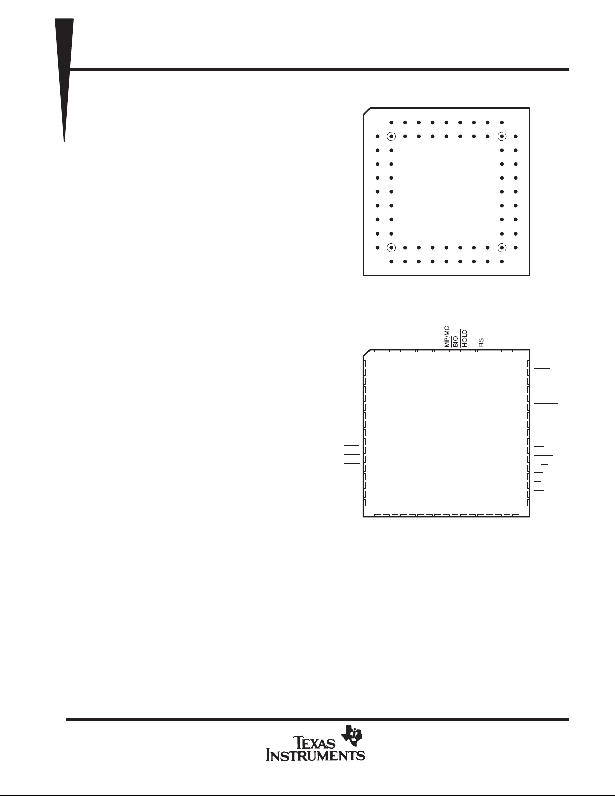
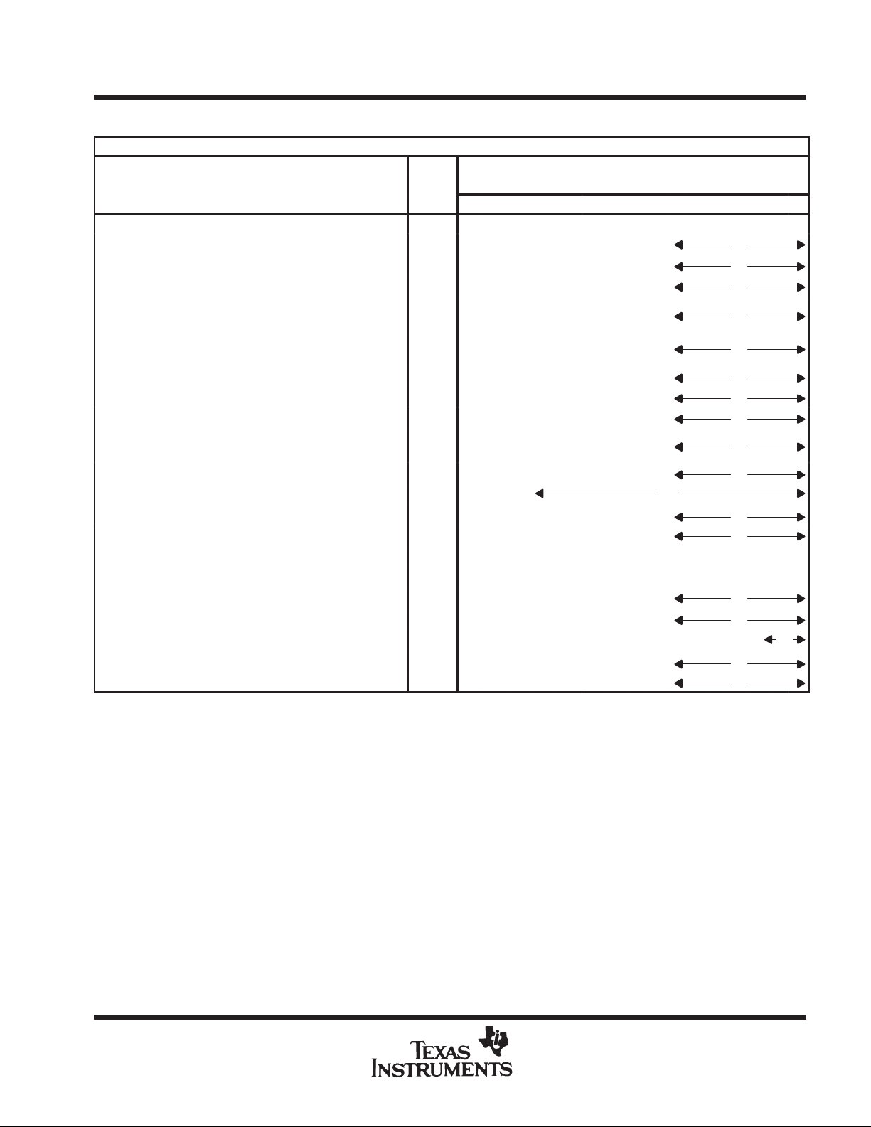
68-Pin GB Package
(Top View)
1234567891011
†
• 4K Words of On-Chip Secure Program
EPROM (TMS320E25)
• 4K Words of On-Chip Program ROM
(TMS320C25)
• 128K Words of Data/Program Space
• 32-Bit ALU/Accumulator
• 16 × 16-Bit Multiplier With a 32-Bit Product
• Block Moves for Data/Program
Management
• Repeat Instructions for Efficient Use of
Program Space
• Serial Port for Direct Codec Interface
• Synchronization Input for Synchronous
Multiprocessor Configurations
• Wait States for Communication to Slow
Off-Chip Memories/Peripherals
• On-Chip Timer for Control Operations
• Single 5-V Supply
• Packaging: 68-Pin PGA, PLCC, and
CER-QUAD
• 68-to-28 Pin Conversion Adapter Socket for
EPROM Programming
• Commercial and Military Versions Available
• NMOS Technology:
— TMS32020 200-ns cycle time. . . . . . . . .
• CMOS Technology:
— TMS320C25 100-ns cycle time. . . . . . . .
— TMS320E25 100-ns cycle time. . . . . . . .
— TMS320C25-50 80-ns cycle time. . . . . .
description
V
SS
D7
D6
D4
D3
D2
D1
D0
SYNC
INT0
INT1
INT2
V
CC
DR
FSR
A0
A
B
C
D
E
F
G
H
J
K
L
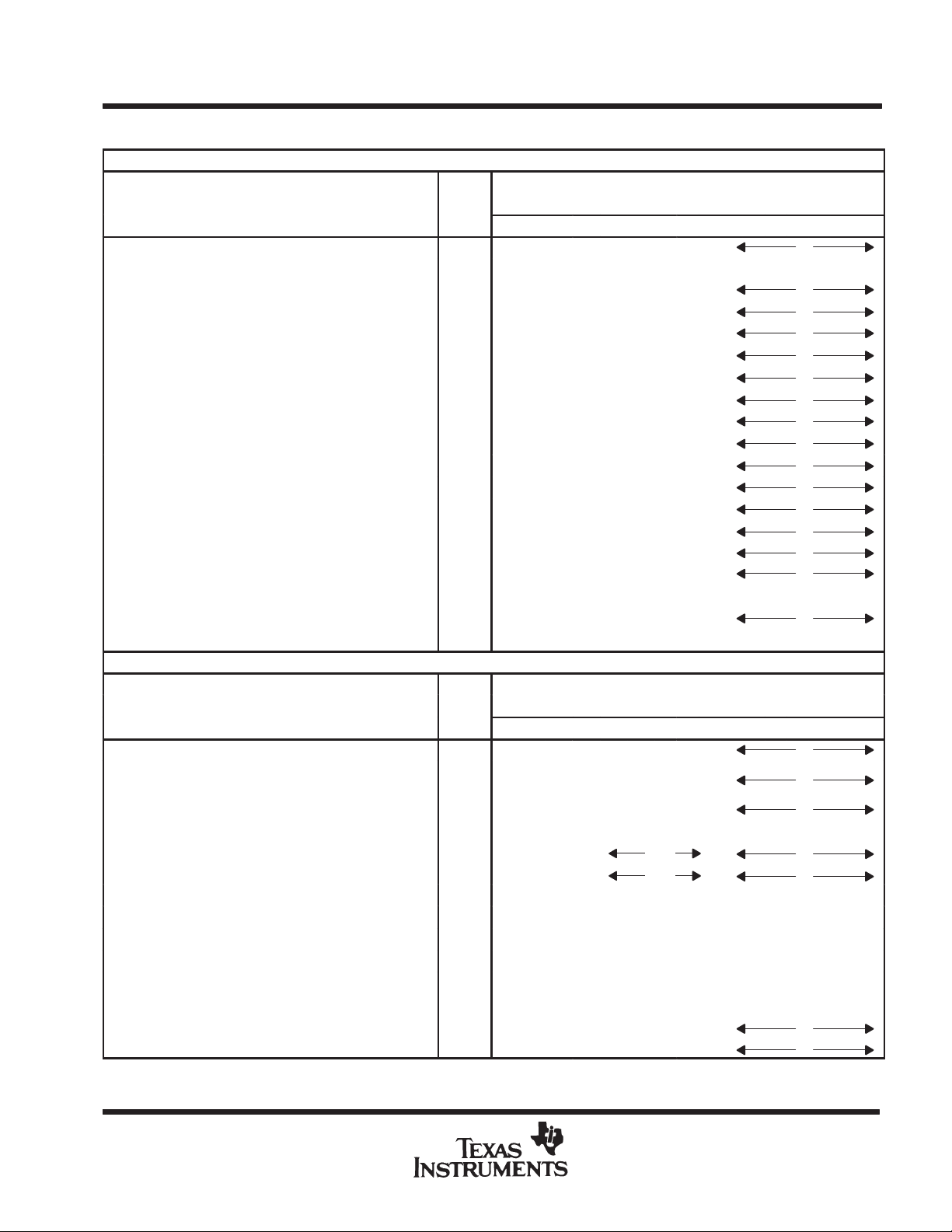
68-Pin FN and FZ Packages
D8D9D10
9 8 7 6 5 4 3 2 1 6867666564636261
10
11
12
D5
13
14
15
16
17
18
19
20
21
22
23
24
25
26
27 28 29 30 31 32 33 34 35 36 37 38 39 40 41 42 43
A1A2A3A4A5A6A7A8A9
SS
V
D11
D12
(Top View)
D13
D14
D15
CC
V
READY
A11
A10
†
CLKR
CLKX
A12
A13
CC
A14
VCCV
60
59
58
57
56
55
54
53
52
51
50
49
48
47
46
45
44
A15
IACK
MSC
CLKOUT1
CLKOUT2
XF
HOLDA
DX
FSX
X2 CLKIN
X1
BR
STRB
R/W
PS
IS
DS
V
SS
ADVANCE INFORMATION
This data sheet provides complete design documentation for the second-generation devices of the TMS320
family . This facilitates the selection of the devices best suited for user applications by providing all specifications
and special features for each TMS320 member. This data sheet is divided into four major sections: architecture,
electrical specifications (NMOS and CMOS), timing diagrams, and mechanical data. In each of these sections,
generic information is presented first, followed by specific device information. An index is provided for quick
reference to specific information about a device.
ADVANCE INFORMATION concerns new products in the
sampling or preproduction phase of development.
Characteristic data and other specifications are subject to
change without notice.
POST OFFICE BOX 1443 • HOUSTON, TEXAS 77001
Copyright 1991, T exas Instruments Incorporated
1
Page 2
TMS320 SECOND-GENERATION
DEVICES
SPRS010B — MA Y 1987—REVISED NOVEMBER 1990
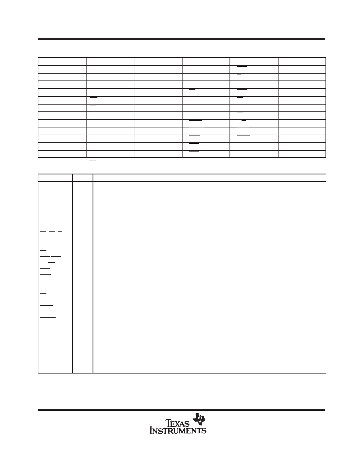
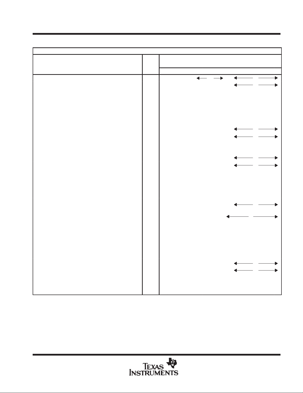
PGA AND PLCC/CER-QUAD PIN ASSIGNMENTS
FUNCTION PIN FUNCTION PIN FUNCTION PIN FUNCTION PIN FUNCTION PIN FUNCTION PIN
A0 K1/26 A12 K8/40 D2 E1/16 D14 A5/3 INT2 H1/22 V
A1 K2/28 A13 L9/41 D3 D2/15 D15 B6/2 IS J11/46 V
A2 L3/29 A14 K9/42 D4 D1/14 DR J1/24 MP/MC†A6/1 V
A3 K3/30 A15 L10/43 D5 C2/13 DS K10/45 MSC C10/59 V
A4 L4/31 BIO B7/68 D6 C1/12 DX E11/54 PS J10/47 V
A5 K4/32 BR G11/50 D7 B2/11 FSR J2/25 READY B8/66 XF D11/56
A6 L5/33 CLKOUT1 C11/58 D8 A2/9 FSX F10/53 RS A8/65 X1 G10/51
A7 K5/34 CLKOUT2 D10/57 D9 B3/8 HOLD A7/67 R/W H11/48 X2/CLKIN F11/52
A8 K6/36 CLKR B9/64 D10 A3/7 HOLDA E10/55 STRB H10/49
A9 L7/37 CLKX A9/63 D11 B4/6 IACK B11/60 SYNC F2/19
A10 K7/38 D0 F1/18 D12 A4/5 INT0 G1/20 V
A11 L8/39 D1 E2/17 D13 B5/4 INT1 G2/21 V
†
On the TMS32020, MP/MC must be connected to VCC.
‡
SIGNALS
V
CC
V
SS
X1
X2/CLKIN
CLKOUT1
CLKOUT2
D15-D0
A15-A0
, DS, IS
PS
R/W
STRB
RS
INT2-INT0
MP/MC
MSC
IACK
READY
BR
XF
HOLD
HOLDA
SYNC
BIO
DR
CLKR
FSR
DX
CLKX
FSX
‡
I/O/Z denotes input/output/high-impedance state.
I/O/Z
O
O
O
I/O/Z
O/Z
O/Z
O/Z
O/Z
O
O
O
O
O
O/Z
I/O/Z
I
5-V supply pins
I
Ground pins
Output from internal oscillator for crystal
I
Input to internal oscillator from crystal or external clock
Master clock output (crystal or CLKIN frequency/4)
A second clock output signal
16-bit data bus D15 (MSB) through D0 (LSB). Multiplexed between program, data, and I/O spaces.
16-bit address bus A15 (MSB) through A0 (LSB)
Program, data, and I/O space select signals
Read/write signal
Strobe signal
I
Reset input
I
External user interrupt inputs
I
Microprocessor/microcomputer mode select pin
Microstate complete signal
Interrupt acknowledge signal
I
Data ready input. Asserted by external logic when using slower devices to indicate that the current bus transaction
is complete.
Bus request signal. Asserted when the TMS320C2x requires access to an external global data memory space.
External flag output (latched software-programmable signal)
I
Hold input. When asserted, TMS320C2x goes into an idle mode and places the data, address, and control lines in
the high impedance state.
Hold acknowledge signal
I
Synchronization input
I
Branch control input. Polled by BIOZ instruction.
I
Serial data receive input
I
Clock for receive input for serial port
I
Frame synchronization pulse for receive input
Serial data transmit output
I
Clock for transmit output for serial port
Frame synchronization pulse for transmit. Configuration as either an input or an output.
DEFINITION
CC
CC
A10/61
B10/62
CC
CC
SS
SS
SS
H2/23
L6/35
B1/10
K11/44
L2/27
2
POST OFFICE BOX 1443 • HOUSTON, TEXAS 77001
Page 3

TMS320 SECOND-GENERATION
DEVICES
SPRS010B — MA Y 1987—REVISED NOVEMBER 1990
description
The TMS320 family of 16/32-bit single-chip digital signal processors combines the flexibility of a high-speed
controller with the numerical capability of an array processor, thereby offering an inexpensive alternative to
multichip bit-slice processors. The highly paralleled architecture and efficient instruction set provide speed and
flexibility to produce a MOS microprocessor family that is capable of executing more than 12.5 MIPS (million
instructions per section). The TMS320 family optimizes speed by implementing functions in hardware that other
processors implement through microcode or software. This hardware-intensive approach provides the design
engineer with processing power previously unavailable on a single chip.
The TMS320 family consists of three generations of digital signal processors. The first generation contains the
TMS32010 and its spinoffs. The second generation includes the TMS32020, TMS320C25, and TMS320E25,
which are described in this data sheet. The TMS320C30 is a floating-point DSP device designed for even higher
performance. Many features are common among the TMS320 processors. Specific features are added in each
processor to provide different cost/performance tradeoffs. Software compatibility is maintained throughout the
family to protect the user’s investment in architecture. Each processor has software and hardware tools to
facilitate rapid design.
introduction
The TMS32010, the first NMOS digital signal processor in the TMS320 family, was introduced in 1983. Its
powerful instruction set, inherent flexibility, high-speed number-crunching capabilities, and innovative
architecture have made this high-performance, cost-effective processor the ideal solution to many
telecommunications, computer, commercial, industrial, and military applications. Since that time, the
TMS320C10, a low-power CMOS version of the industry-standard TMS32010, and other spinoff devices have
been added to the first generation of the TMS320 family.
The second generation of the TMS320 family (referred to as TMS320C2x) includes four members, the
TMS32020, TMS320C25, TMS320C25-50, and TMS320E25. The architecture of these devices is based upon
that of the TMS32010.
The TMS32020, processed in NMOS technology, is source-code compatible with he TMS32010 and in many
applications is capable of two times the throughput of the first-generation devices. Its enhanced instruction set
(109 instructions), large on-chip data memory (544 words), large memory spaces, on-chip serial port, and
hardware timer make the TMS32020 a powerful addition to the TMS320 family.
The TMS320C25 is the second member of the TMS320 second generation. It is processed in CMOS technology,
is capable of an instruction cycle time of 100 ns, and is pin-for-pin and object-code compatible with the
TMS32020. The TMS320C25’s enhanced feature set greatly increases the functionality of the device over the
TMS32020. Enhancements included 24 additional instructions (133 total), eight auxiliary registers, an
eight-level hardware stack, 4K words of on-chip program ROM, a bit-reversed indexed-addressing mode, and
the low-power dissipation inherent to the CMOS process. An extended-temperature range version
(TMS320C25GBA) is also available.
The TMS320C25-50 is a high-speed version of the TMS320C25. It is capable of an instruction cycle time of less
than 80 ns. It is architecturally identical to the original 40-MHz version of the TMS320C25 and, thus, is pin-for-pin
and object-code compatible with the TMS320C25.
The TMS320E25 is identical to the TMS320C25, with the exception that the on-chip 4K-word program ROM is
replaced with a 4K-word on-chip program EPROM. On-chip EPROM allows realtime code development and
modification for immediate evaluation of system performance.
POST OFFICE BOX 1443 • HOUSTON, TEXAS 77001
3
Page 4
TMS320 SECOND-GENERATION
DEVICES
SPRS010B — MA Y 1987—REVISED NOVEMBER 1990
Key Features: TMS32020
• 200-ns Instruction Cycle Time
• 544 Words of On-Chip Data RAM
• 128K Words of Total Data/Program
Memory Space
• Wait States for Communication to Slower Off-Chip
Memories
• Source Code Compatible With the TMS320C1x
• Single-Cycle Multiply/Accumulate Instructions
• Repeat Instructions
• Global Data Memory Interface
• Block Moves for Data/Program Management
• Five Auxiliary Registers With Dedicated
Arithmetic Unit
• Serial Port for Multiprocessing or Interfacing
to Codecs, Serial Analog-to-Digital
Converters, etc.
Key Features: TMS320C25, TMS320C25-50, TMS320E25
• 80-ns Instruction Cycle Time (TMS320C25-50)
• 100-ns Instruction Cycle Time (TMS320C25)
• 4K Words of On-Chip Secure Program EPROM
(TMS320E25)
• 4K Words of On-Chip Program
ROM (TMS320C25)
• 544 Words of On-Chip RAM
• 128K Words of Total Program/Data
Memory Space
• Wait States for Communications to
Slower Off-Chip Memories
• Object-Code Compatible With the TMS32020
• Source-Code Compatible W ith TMS320C1x
• 24 Additional Instructions to Support
Adaptive Filtering, FFTs, and
Extended-Precision Arithmetic
• Block Moves for Data/Program Management
• Single-Cycle Multiply/Accumulate Instructions
• Eight Auxiliary Registers W ith Dedicated
Arithmetic Unit
• Bit-Reversed Indexed-Addressing Mode for
Radix-2 FFTS
• Double-Buffered Serial Port
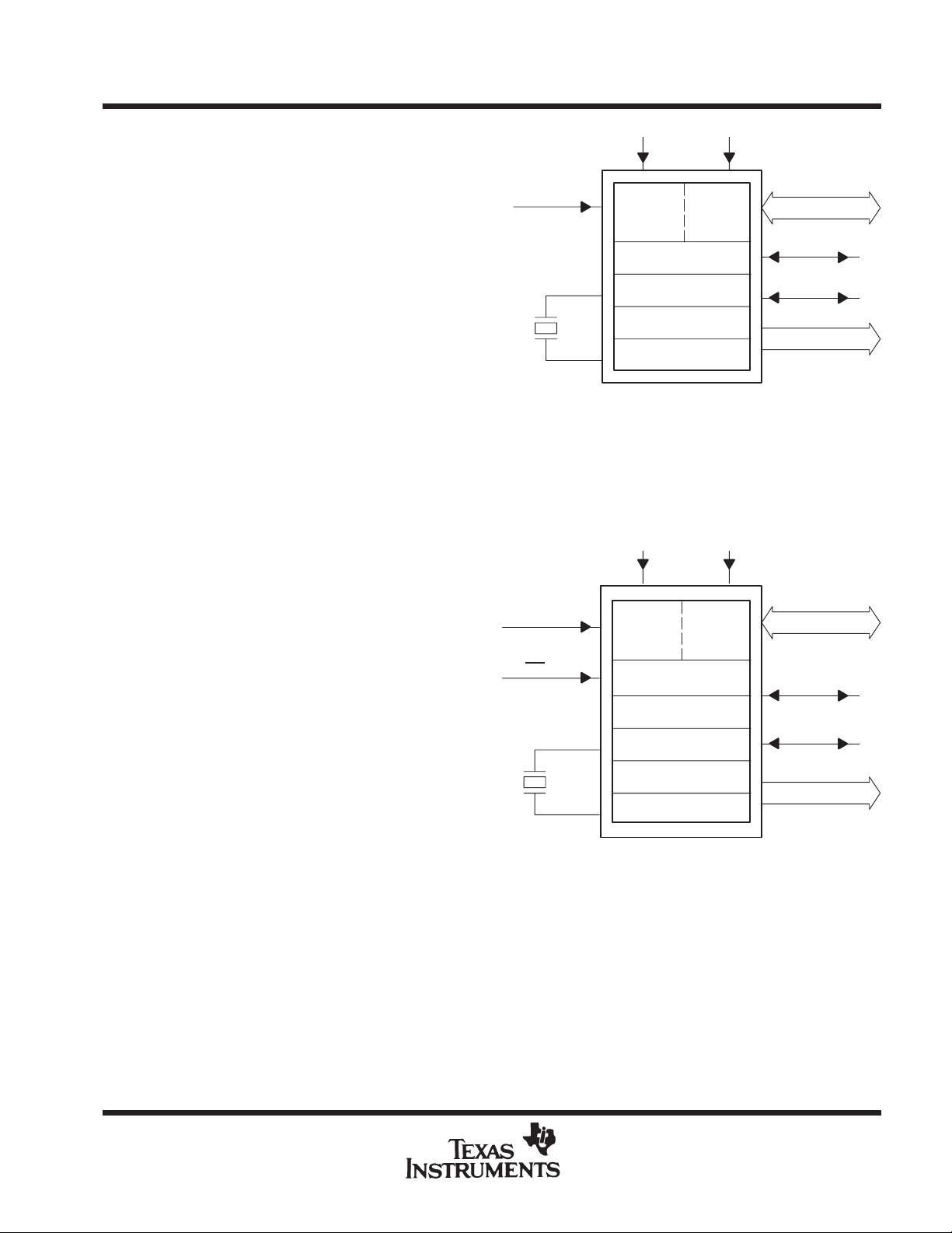
+5 V GND
Interrupts
256-Word
Data/Prog
RAM
32-BIT ALU/ACC
288-Word
Multiplier
Shifters
Timer
Data
RAM
Data (16)
Multi-
Processor
Interface
Serial
Interface
Address (16)
• On-Chip Clock Generator
• Single 5-V Supply
• NMOS Technology
• 68-Pin Grid Array (PGA) Package
+5 V GND
Interrupts
MP/MC
256-Word
Data/Prog
RAM
32-Bit ALU/ACC
288-Word
Data
RAM
4K-Words
ROM/EPROM
Multiplier
Shifters
Timer
Data (16)
Multi-
Processor
Interface
Serial
Interface
Address (16)
• On-Chip Clock Generator
• Single 5-V Supply
• Internal Security Mechanism (TMS320E25)
• 68-to-28 Pin Conversion Adapter Socket
• CMOS Technology
• 68-Pin Grid Array (PGA) Package
(TMS320C25)
• 68-Lead Plastic Leaded Chip Carrier (PLCC)
Package (TMS320C25, TMS320C25-50)
• 68-Lead CER-QUAD Package (TMS320E25)
4
POST OFFICE BOX 1443 • HOUSTON, TEXAS 77001
Page 5
TMS320 SECOND-GENERATION
DEVICES
SPRS010B — MA Y 1987—REVISED NOVEMBER 1990
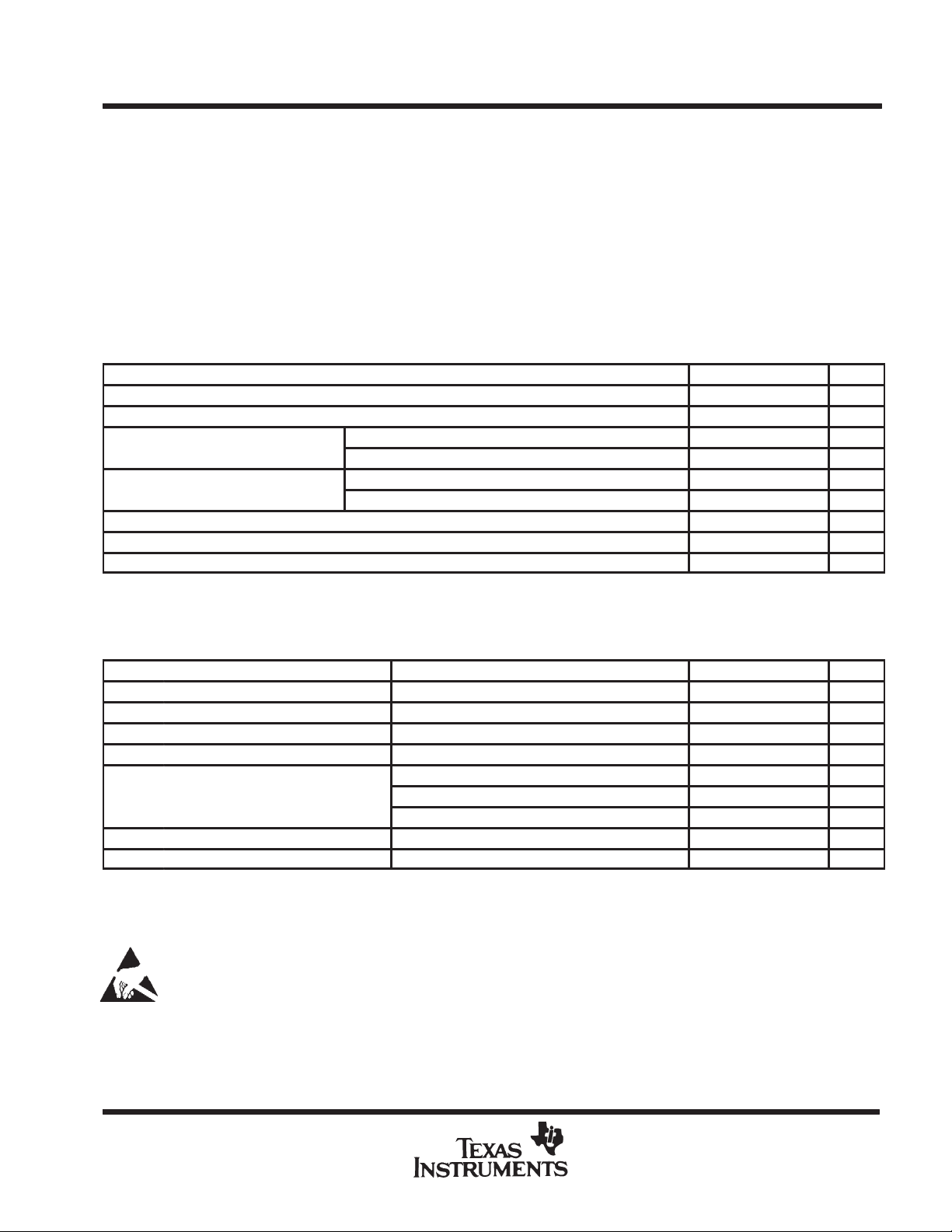
T able 1 provides an overview of the second-generation TMS320 processors with comparisons of memory, I/O,
cycle timing, power, package type, technology , and military support. For specific availability , contact the nearest
TI Field Sales Office.
Table 1. TMS320 Second-Generation Device Overview
MEMORY
DEVICE
‡
TMS32020
TMS320C25
TMS320C25-50§(CMOS) 544 4K 64K 64K YES
TMS320E25
†
SER = serial; PAR = parallel; DMA = direct memory access; CON = concurrent DMA.
‡
Military version available; contact nearest TI Field Sales Office for availability .
§
Military version planned; contact nearest TI Field Sales Office for details.
(NMOS) 544 — 64K 64K YES
‡
(CMOS) 544 4K 64K 64K YES
§
(CMOS) 544 4K 64K 64K YES
ON-CHIP OFF-CHIP
RAM ROM/EPROM PROG DATA
SER PAR DMA PGA PLCC CER-QUAD
I/O
16 × 16
16 × 16
16 × 16
16 × 16
†
YES YES 200 1250 68 — —
CON YES 100 500 68 68 —
CON YES 80 500 — 68 —
CON YES 100 500 — — 68
TIMER
CYCLE
TIME
(ns)
TYP
POWER
(mW)
PACKAGE
TYPE
architecture
The TMS320 family utilizes a modified Harvard architecture for speed and flexibility. In a strict Harvard
architecture, program and data memory lie in two separate spaces, permitting a full overlap of instruction fetch
and execution. The TMS320 family’s modification of the Harvard architecture allows transfers between program
and data spaces, thereby increasing the flexibility of the device. This modification permits coefficients stored
in program memory to be read into the RAM, eliminating the need for a separate coefficient ROM. It also makes
available immediate instructions and subroutines based on computed values.
Increased throughput on the TMS320C2x devices for many DSP applications is accomplished by means of
single-cycle multiply/accumulate instructions with a data move option, up to eight auxiliary registers with a
dedicated arithmetic unit, and faster I/O necessary for data-intensive signal processing.
The architectural design of the TMS320C2x emphasizes overall speed, communication, and flexibility in
processor configuration. Control signals and instructions provide floating-point support, block-memory
transfers, communication to slower off-chip devices, and multiprocessing implementations.
32-bit ALU/accumulator
The 32-bit Arithmetic Logic Unit (ALU) and accumulator perform a wide range of arithmetic and logical
instructions, the majority of which execute in a single clock cycle. The ALU executes a variety of branch
instructions dependent on the status of the ALU or a single bit in a word. These instructions provide the following
capabilities:
• Branch to an address specified by the accumulator
• Normalize fixed-point numbers contained in the accumulator
• Test a specified bit of a word in data memory
One input to the ALU is always provided from the accumulator, and the other input may be provided from the
Product Register (PR) of the multiplier or the input scaling shifter which has fetched data from the RAM on the
data bus. After the ALU has performed the arithmetic or logical operations, the result is stored in the accumulator.
The 32-bit accumulator is split into two 16-bit segments for storage in data memory. Additional shifters at the
output of the accumulator perform shifts while the data is being transferred to the data bus for storage. The
contents of the accumulator remain unchanged.
POST OFFICE BOX 1443 • HOUSTON, TEXAS 77001
5
Page 6
TMS320 SECOND-GENERATION
DEVICES
SPRS010B — MA Y 1987—REVISED NOVEMBER 1990
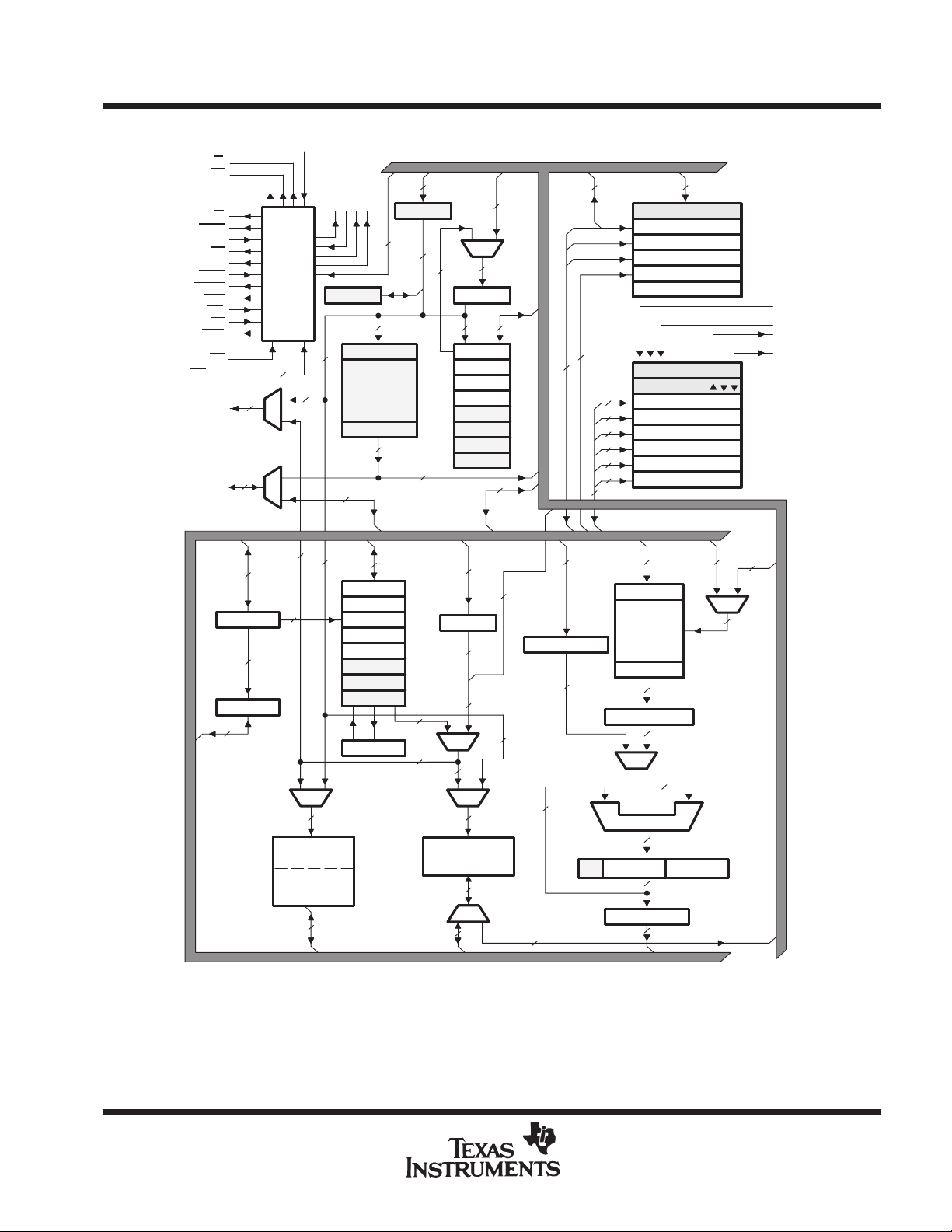
functional block diagram (TMS320C2x)
SYNC
IS
DS
PS
X1
X2/CLKIN
CLKOUT1
MCS(16)
(4096
Instruction
16
CLKOUT2
16
16
16 16 16
Address
Program
ROM/
EPROM
× 16)
16
Data Bus
R/W
STRB
READY
BR
XF
HOLD
HOLDA
MSC
BIO
RS
IACK
MP/MC
INT(2-0)
A15-A0
D15-D0
Controller
16
3
16
16
16
MUXMUX
16
PFC(16)
16
16
MUX
PC(16)
Stack
(8 x 16)
Program Bus
16
16
16 16
QIR(16)
IR(16)
STO(16)
ST1(16)
RPTC(8)
IFR(6)
RSR(16)
16
16
16
16
6
8
16
XSR(16)
DRR(16)
DXR(16)
TIM(16)
PRD(16)
IMR(6)
GREG(8)
Program Bus
DR
CLKR
FSR
DX
CLKX
FSX
16
16
16
16
3
MUX
Block B2
× 16)
(32
Data RAM
Block B1
(256
16
16
× 16)
16
3
ARP(3)
3
ARB(3)
3
LEGEND:
ACCH = Accumulator high IFR = Interrupt flag register PC = Program counter
ACCL = Accumulator low IMR = Interrupt mask register PFC = Prefetch counter
ALU = Arithmetic logic unit IR = Instruction register RPTC = Repeat instruction counter
ARAU = Auxiliary register arithmetic unitMCS = Microcall stack GREG = Global memory allocation register
ARB = Auxiliary register pointer buffer QIR = Queue instruction register RSR = Serial port receive shift register
ARP = Auxiliary register pointer PR = Product register XSR = Serial port transmit shift register
DP = Data memory page pointer PRD = Period register for timer AR0-AR7 = Auxiliary registers
DRR = Serial port data receive registerTIM = Timer ST0, ST1 = Status registers
DXR = Serial port data transmit register TR = Temporary register C = Carry bit
AR0(16)
AR1(16)
AR2(16)
AR3(16)
AR4(16)
AR5(16)
AR6(16)
AR7(16)
ARAU(16)
Data Bus
16
16
16
DP(9)
MUX
16
MUX
DATA/PROG
RAM (256
Block B0
MUX
16
9
9
16
16
× 16)
16
7 LSB
From IR
16
16
Shifter(0-16)
32
32
16
Shifter(-6, 0, 1, 4)
C
ACCH(16)
Shifters (0-7)
16
TR(16)
Multiplier
PR(32)
32
32
MUX
32
ALU(32)
32
ACCL(16)
32
†
16
16
MUX
16
16
6
POST OFFICE BOX 1443 • HOUSTON, TEXAS 77001
Page 7

TMS320 SECOND-GENERATION
DEVICES
SPRS010B — MA Y 1987—REVISED NOVEMBER 1990
scaling shifter
The TMS320C2x scaling shifter has 16-bit input connected to the data bus and a 32-bit output connected to the
ALU. The scaling shifter produces a left shift of 0 to 16 bits on the input data, as programmed in the instruction.
The LSBs of the output are filled with zeroes, and the MSBs may be either filled with zeroes or sign-extended,
depending upon the status programmed into the SXM (sign-extension mode) bit of status register ST1.
16 × 16-bit parallel multiplier
The 16 × 16-bit hardware multiplier is capable of computing a signed or unsigned 32-bit product in a single
machine cycle. The multiplier has the following two associated registers.
• A 16-bit Temporary Register (TR) that holds one of the operands for the multiplier, and
• A 32-bit Product Register (PR) that holds the product.
Incorporated into the instruction set are single-cycle multiply/accumulate instructions that allow both operands
to be processed simultaneously. The data for these operations may reside anywhere in internal or external
memory, and can be transferred to the multiplier each cycle via the program and data buses.
Four product shift modes are available at the Product Register (PR) output that are useful when performing
multiply/accumulate operations, fractional arithmetic, or justifying fractional products.
timer
The TMS320C2x provides a memory-mapped 16-bit timer for control operations. The on-chip timer (TIM)
register is a down counter that is continuously clocked by CLKOUT1 on the TMS320C25. The timer is clocked
by CLKOUT1/4 on the TMS32020. A timer interrupt (TINT) is generated every time the timer decrements to zero.
The timer is reloaded with the value contained in the period (PRD) register within the next cycle after it reaches
zero so that interrupts may be programmed to occur at regular intervals of PRD + 1 cycles of CLKOUT 1 on the
TMS320C25 or 4 × PRD × CLKOUT 1 cycles on the TMS32020.
memory control
The TMS320C2x provides a total of 544 16-bit words of on-chip data RAM, divided into three separate blocks
(B0, B1, and B2). Of the 544 words, 288 words (blocks B1 and B2) are always data memory, and 256 words
(block B0) are programmable as either data or program memory . A data memory size of 544 words allows the
TMS320C2x to handle a data array of 512 words (256 words if on-chip RAM is used for program memory), while
still leaving 32 locations for intermediate storage. When using block B0 as program memory, instructions can
be downloaded from external program memory into on-chip RAM and then executed.
When using on-chip program RAM, ROM, EPROM, or high-speed external program memory , the TMS320C2x
runs at full speed without wait states. However, the READY line can be used to interface the TMS320C2x to
slower, less-expensive external memory . Downloading programs from slow off-chip memory to on-chip program
RAM speeds processing while cutting system costs.
The TMS320C2x provides three separate address spaces for program memory, data memory, and I/O. The
on-chip memory is mapped into either the 64K-word data memory or program memory space, depending upon
the memory configuration (see Figure 1). The CNFD (configure block B0 as data memory) and CNFP (configure
block B0 as program memory) instructions allow dynamic configuration of the memory maps through software.
Regardless of the configuration, the user may still execute from external program memory.
The TMS320C2x has six registers that are mapped into the data memory space: a serial port data receive
register, serial port data transmit register, timer register, period register, interrupt mask register, and global
memory allocation register.
POST OFFICE BOX 1443 • HOUSTON, TEXAS 77001
7
Page 8
TMS320 SECOND-GENERATION
DEVICES
SPRS010B — MA Y 1987—REVISED NOVEMBER 1990
0(0000h)
31(001Fh)
32(0020h)
65,535(FFFFh)
If MP/MC
(Microprocessor Mode)
Program Program Data
Interrupts
and Reserved
(External)
External
= 1
Interrupts
and Reserved
(On-Chip
31(001Fh)
32(0020h)
4015(0FAFh)
4016(0FB0h)
4095(0FFFh)
4096(1000h)
65,535(0FFFFh)
ROM/EPROM)
On-Chip
ROM/EPROM
Reserved
External
If MP/MC = 0
(Microcomputer Mode on TMS320C25)
0(0000h)0(0000h)
5(0005h)
6(0006h)
95(005Fh)
96(0060h)
127(007Fh)
128(0080h)
511(01FFh)
512(0200h)
767(02FFh)
768(0300h)
1023(03FFh)
1024(0400h)
65,535(0FFFFh)
(a) Memory Maps After a CNFD Instruction
On-Chip
Memory-Mapped
Registers
Reserved
On-Chip
Block B2
Reserved
On-Chip
Block B0
On-Chip
Block B1
External
Page 0
Pages 1-3
Pages 4-5
Pages 6 -7
Pages 8 -511
0(0000h)
31(001Fh)
32(0020h)
65,279(0FEFFh)
65,280(0FF00h)
65,535(0FFFFh)
If MP/MC
(Microprocessor Mode)
Program Program Data
Interrupts
and Reserved
(External)
Block B0
= 1
External
On-Chip
0(0000h)
31(001Fh)
32(0020h)
4015(0FAFh)
4016(0FB0h)
4095(0FFFh)
4096(1000h)
65,279(0FEFFh)
65,280(0FF00h)
65,535(0FFFFh)
If MP/MC
(Microcomputer Mode on TMS320C25)
Interrupts
and Reserved
(On-Chip
ROM/EPROM)
On-Chip
ROM/EPROM
Reserved
External
On-Chip
Block B0
= 0
0(0000h)
5(0005h)
6(0006h)
95(005Fh)
96(0060h)
127(007Fh)
128(0080h)
511(01FFh)
512(0200h)
767(02FFh)
768(0300h)
1023(03FFh)
1024(0400h)
65,535(0FFFFh)
(b) Memory Maps After a CNFP Instruction
On-Chip
Memory-Mapped
Registers
Reserved
On-Chip
Block B2
Reserved
Does Not
Exist
On-Chip
Block B1
External
Page 0
Pages 1-3
Pages 4-5
Pages 6 -7
Pages 8 -511
Figure 1. Memory Maps
8
POST OFFICE BOX 1443 • HOUSTON, TEXAS 77001
Page 9

TMS320 SECOND-GENERATION
DEVICES
SPRS010B — MA Y 1987—REVISED NOVEMBER 1990
interrupts and subroutines
The TMS320C2x has three external maskable user interrupts INT2-INT0, available for external devices that
interrupt the processor. Internal interrupts are generated by the serial port (RINT and XINT), by the timer (TINT),
and by the software interrupt (TRAP) instruction. Interrupts are prioritized with reset (RS
priority and the serial port transmit interrupt (XINT) having the lowest priority. All interrupt locations are on
two-word boundaries so that branch instructions can be accommodated in those locations if desired.
A built-in mechanism protects multicycle instructions from interrupts. If an interrupt occurs during a multicycle
instruction, the interrupt is not processed until the instruction is completed. This mechanism applies to
instructions that are repeated and to instructions that become multicycle due to the READY signal.
external interface
The TMS320C2x supports a wide range of system interfacing requirements. Program, data, and I/O address
spaces provide interface to memory and I/O, thus maximizing system throughput. I/O design is simplified by
having I/O treated the same way as memory. I/O devices are mapped into the I/O address space using the
processor’s external address and data buses in the same manner as memory-mapped devices. Interface to
memory and I/O devices of varying speeds is accomplished by using the READY line. When transactions are
made with slower devices, the TMS320C2x processor waits until the other device completes its function and
signals the processor via the READY line. Then, the TMS320C2x continues execution.
A full-duplex serial port provides communication with serial devices, such as codecs, serial A/D converters, and
other serial systems. The interface signals are compatible with codecs and many other serial devices with a
minimum of external hardware. The serial port may also be used for intercommunication between processors
in multiprocessing applications.
) having the highest
The serial port has two memory-mapped registers: the data transmit register (DXR) and the data receive register
(DRR). Both registers operate in either the byte mode or 16-bit word mode, and may be accessed in the same
manner as any other data memory location. Each register has an external clock, a framing synchronization
pulse, and associated shift registers. One method of multiprocessing may be implemented by programming one
device to transmit while the others are in the receive mode. The serial port on the TMS320C25 is double-buffered
and fully static.
multiprocessing
The flexibility of the TMS320C2x allows configurations to satisfy a wide range of system requirements and can
be used as follows:
• A standalone processor
• A multiprocessor with devices in parallel
• A slave/host multiprocessor with global memory space
• A peripheral processor interfaced via processor-controlled signals to another device.
For multiprocessing applications, the TMS320C2x has the capability of allocating global data memory space
and communicating with that space via the BR (bus request) and READY control signals. Global memory is data
memory shared by more than one processor. Global data memory access must be arbitrated. The 8-bit
memory-mapped GREG (global memory allocation register) specifies part of the TMS320C2x’s data memory
as global external memory . The contents of the register determine the size of the global memory space. If the
current instruction addresses an operand within that space, BR is asserted to request control of the bus. The
length of the memory cycle is controlled by the READY line.
The TMS320C2x supports DMA (direct memory access) to its external program/data memory using the HOLD
and HOLDA signals. Another processor can take complete control of the TMS320C2x’s external memory by
asserting HOLD
high-impedance state, and assert HOLDA. On the TMS320C2x, program execution from on-chip ROM may
proceed concurrently when the device is in the hold mode.
low. This causes the TMS320C2x to place its address data and control lines in a
POST OFFICE BOX 1443 • HOUSTON, TEXAS 77001
9
Page 10

TMS320 SECOND-GENERATION
DEVICES
SPRS010B — MA Y 1987—REVISED NOVEMBER 1990
instruction set
The TMS320C2x microprocessor implements a comprehensive instruction set that supports both
numeric-intensive signal processing operations as well as general-purpose applications, such as
multiprocessing and high-speed control. The TMS32020 source code is upward-compatible with TMS320C25
source code. TMS32020 object code runs directly on the TMS320C25.
For maximum throughput, the next instruction is prefetched while the current one is being executed. Since the
same data lines are used to communicate to external data/program or I/O space, the number of cycles may vary
depending upon whether the next data operand fetch is from internal or external memory . Highest throughput
is achieved by maintaining data memory on-chip and using either internal or fast external program memory.
addressing modes
The TMS320C2x instruction set provides three memory addressing modes: direct, indirect, and immediate
addressing.
Both direct and indirect addressing can be used to access data memory . In direct addressing, seven bits of the
instruction word are concatenated with the nine bits of the data memory page pointer to form the 16-bit data
memory address. Indirect addressing accesses data memory through the auxiliary registers. In immediate
addressing, the data is based on a portion of the instruction word(s).
In direct memory addressing, the instruction word contains the lower seven bits of the data memory address.
This field is concatenated with the nine bits of the data memory page pointer to form the full 16-bit address. Thus,
memory is paged in the direct addressing mode with a total of 512 pages, each page containing 128 words.
Up to eight auxiliary registers (AR0-AR7) provide flexible and powerful indirect addressing (five on the
TMS32020, eight on the TMS320C25). To select a specific auxiliary register, the Auxiliary Register Pointer
(ARP) is loaded with a value from 0 to 7 for AR0 through AR7, respectively.
There are seven types of indirect addressing: auto-increment or auto-decrement, post-indexing by either adding
or subtracting the contents of AR0, single indirect addressing with no increment or decrement, and bit-reversal
addressing (used in FFT s on the TMS320C25 only) with increment or decrement. All operations are performed
on the current auxiliary register in the same cycle as the original instruction, following which the current auxiliary
register and ARP may be modified.
repeat feature
A repeat feature, used with instructions such as multiply/accumulates, block moves, I/O transfers, and table
read/writes, allows a single instruction to be performed up to 256 times. The repeat counter (RPTC) is loaded
with either a data memory value (RPT instruction) or an immediate value (RPTK instruction). The value of this
operand is one less than the number of times that the next instruction is executed. Those instructions that are
normally multicycle are pipelined when using the repeat feature, and effectively become single-cycle
instructions.
10
POST OFFICE BOX 1443 • HOUSTON, TEXAS 77001
Page 11

TMS320 SECOND-GENERATION
DEVICES
SPRS010B — MA Y 1987—REVISED NOVEMBER 1990
instruction set summary
Table 2 lists the symbols and abbreviations used in Table 3, the TMS320C25 instruction set summary. Table 3
consists primarily of single-cycle, single-word instructions. Infrequently used branch, I/O, and CALL instructions
are multicycle. The instruction set summary is arranged according to function and alphabetized within each
functional grouping. The symbol (
instruction set. The symbol (‡) indicates instructions that are not included in the TMS32020 instruction set.
SYMBOL DEFINITION
B
CM
D
FO
I
K
PA
PM
AR
S
X
†
) indicates those instructions that are not included in the TMS320C1x
Table 2. Instruction Symbols
4-bit field specifying a bit code
2-bit field specifying compare mode
Data memory address field
Format status bit
Addressing mode bit
Immediate operand field
Port address (PA0 through P A15 are predefined assembler symbols
equal to 0 through 15, respectively .)
2-bit field specifying P register output shift code
3-bit operand field specifying auxiliary register
4-bit left-shift code
3-bit accumulator left-shift field
POST OFFICE BOX 1443 • HOUSTON, TEXAS 77001
11
Page 12
TMS320C25
SPRS010B — MA Y 1987—REVISED NOVEMBER 1990
Table 3. TMS320C25 Instruction Set Summary
ACCUMULATOR MEMORY REFERENCE INSTRUCTIONS
MNEMONIC
ABS Absolute value of accumulator 1 1 1 0 0 1 1 1 0 0 0 0 1 1 0 1 1
ADD Add to accumulator with shift 1 0 000 I
‡
ADDC
ADDH Add to high accumulator 1 0 1001000I
ADDK
ADDS
ADDT
ADLK
AND AND with accumulator 1 0 1001110I
ANDK
CMPL
LAC Load accumulator with shift 1 0 010 I
LACK Load accumulator immediate short 1 1 1001010
LACT
LALK
†
NEG
NORM
OR OR with accumulator 1 0 1001101I
†
ORK
‡
ROL
‡
ROR
SACH Store high accumulator with shift 1 0 1101 I
SACL Store low-order accumulator with shift 1 0 1100 I
SBLK†
†
SFL
†
SFR
SUB Subtract from accumulator with shift 1 0 001 I
SUBB
SUBC Conditional subtract 1 0 1000111I
SUBH Subtract from high accumulator 1 0 1000100I
SUBK
SUBS
†
These instructions are not included in the TMS320C1x instruction set.
‡
These instructions are not included in the TMS32020 instruction set.
Add to accumulator with carry 1 0 1000011I
‡
Add to accumulator short immediate 1 1 1001100
Add to low accumulator with sign
extension suppressed
Add to accumulator with shift specified by
T register
†
Add to accumulator long immediate with shift 2 1 1 0 1 00000010
†
AND immediate with accumulator with shift 2 1 1 0 1 00000100
†
Complement accumulator 1 1 100111000100111
Load accumulator with shift specified by
†
T register
†
Load accumulator long immediate with shift 2 1 1 0 1 00000001
Negate accumulator 1 1 100111000100011
†
Normalize contents of accumulator 1 1 10011101XXX0010
OR immediate with accumulator with shift 2 1 1 0 1 00000101
Rotate accumulator left 1 1 100111000110100
Rotate accumulator right 1 1 100111000110101
Subtract from accumulator long immediate
with shift
Shift accumulator left 1 1 100111000011000
Shift accumulator right 1 1 100111000011001
‡
Subtract from accumulator with borrow 1 0 1001111I
‡
Subtract from accumulator short immediate 1 1 1001101
Subtract from low accumulator with sign
extension suppressed
DESCRIPTION
NO.
WORDS
15 14 13 12 11 10 9 8 7 6 5 4 3 2 1 0
1
0 1001001I
1
0 1001010I
1
0 1000010I
2
1 1 0 1 00000011
1 0 1 0 0 0 1 0 1 I
INSTRUCTION BIT CODE
S
S
S
S
S
S
X D
S
S D
D
D
D
K
D
D
D
D
K
D
D
DX
D
D
D
K
D
12
POST OFFICE BOX 1443 • HOUSTON, TEXAS 77001
Page 13
SPRS010B — MA Y 1987—REVISED NOVEMBER 1990
Table 3. TMS320C25 Instruction Set Summary (continued)
ACCUMULATOR MEMORY REFERENCE INSTRUCTIONS
TMS320C25
MNEMONIC
Subtract from accumulator with shift specified by
†
SUBT
XOR Exclusive-OR with accumulator 1 0 1001100I
XORK
ZAC Zero accumulator 1 1 100101000000000
ZALH Zero low accumulator and load high accumulator 1 0 1000000I
ZALR
ZALS
MNEMONIC
ADRK‡Add to auxiliary register short immediate 1 0 1 1 1 1 1 1 0
CMPR
LAR Load auxiliary register 1 0 0110 I
LARK Load auxilliary register short immediate 1 1 1000
LARP Load auxilliary register pointer 1 0 101010110001
LDP Load data memory page pointer 1 0 1010010I
LDPK Load data memory page pointer immediate 1 1 100100
LRLK†Load auxiliary register long immediate 2 1 1010 00000000
MAR Modify auxiliary register 1 0 1010101I
SAR Store auxiliary register 1 0 1110 I
SBRK‡Subtract from auxiliary register short immediate 1 0 1 1 1 1 1 1 1
†
These instructions are not included in the TMS320C1x instruction set.
‡
These instructions are not included in the TMS32020 instruction set.
T register
Exclusive-OR immediate with accumulator with
†
shift
Zero low accumulator and load high accumulator
‡
with rounding
Zero accumulator and load low accumulator with
sign extension suppressed
Compare auxiliary register with auxiliary
†
register AR0
DESCRIPTION
AUXILIARY REGISTERS AND DATA PAGE POINTER INSTRUCTIONS
DESCRIPTION
NO.
WORDS
WORDS
15 14 13 12 11 10 9 8 7 6 5 4 3 2 1 0
1 0 1 0 0 0 1 1 0 I
1 1 0 1 00000110
2
0 1111011I
1
1
0 1000001I
NO.
15 14 13 12 11 10 9 8 7 6 5 4 3 2 1 0
1 1001110010100
1
INSTRUCTION BIT CODE
D
D
S
D
D
D
INSTRUCTION BIT CODE
K
CM
DR
KR
R
D
DP
R
D
DR
K
POST OFFICE BOX 1443 • HOUSTON, TEXAS 77001
13
Page 14
TMS320C25
SPRS010B — MA Y 1987—REVISED NOVEMBER 1990
Table 3. TMS320C25 Instruction Set Summary (continued)
T REGISTER, P REGISTER, AND MULTIPLY INSTRUCTIONS
MNEMONIC
APAC Add P register to accumulator 1 1 1 0 0 1 1 1 0 0 0 0 1 0 1 0 1
†
LPH
LT Load T register 1 0 0111100I
LTA Load T register and accumulate previous product 1 0 0111101I
LTD
LTP
LTS
MAC†Multiply and accumulate 2 0 1011101I
MACD†Multiply and accumulate with data move 2 0 1011100I
MPY
MPYA‡Multiply and accumulate previous product 1 0 0111010I
MPYK Multiply immediate 1 1 01
MPYS‡
MPYU‡
PAC Load accumulator with P register 1 1 100111000010100
SPAC Subtract P register from accumulator 1 1 100111000010110
SPH
SPL
SPM
SQRA†Square and accumulate 1 0 0111001I
SQRS†Square and subtract previous product 1 0 1 0 1 1 0 1 0 I
†
These instructions are not included in the TMS320C1x instruction set.
‡
These instructions are not included in the TMS32020 instruction set.
Load high P register 1 0 1010011I
Load T register, accumulate previous product,
and move data
Load T register and store P register in
†
accumulator
†
Load T register and subtract previous product 1 0 1011011I
Multiply (with T register, store product in
P register)
Multiply and subtract previous product 1 0 0111011I
Multiply unsigned 1 1 1001111I
‡
Store high P register 1 0 1111101I
‡
Store low P register 1 0 1111100I
†
Set P register output shift mode 1 1 1001110000010
DESCRIPTION
NO.
WORDS
1
1
1
15 14 13 12 11 10 9 8 7 6 5 4 3 2 1 0
0 0111111I
0 0111110I
0 0111000I
INSTRUCTION BIT CODE
D
D
D
D
D
D
D
D
D
D
K
D
D
D
D
PM
D
D
14
POST OFFICE BOX 1443 • HOUSTON, TEXAS 77001
Page 15
SPRS010B — MA Y 1987—REVISED NOVEMBER 1990
Table 3. TMS320C25 Instruction Set Summary (continued)
BRANCH/CALL INSTRUCTIONS
TMS320C25
MNEMONIC
B Branch unconditionally 2 1 1 1 1 1 1 1 1 1
BACC†Branch to address specified by accumulator 1 1 100111000100101
BANZ Branch on auxiliary register not zero 2 1 11110111
BBNZ†Branch if TC bit ≠ 021 11110011
†
BBZ
BC
BGEZ Branch if accumulator ≥ 021 11101001
BGZ Branch if accumulator > 0 2 1 11100011
BIOZ Branch on I/O status = 0 2 1 11110101
BLEZ Branch if accumulator ≤ 021 11100101
BLZ Branch if accumulator < 0 2 1 11100111
BNC‡Branch on no carry 2 0 10111111
BNV†Branch if no overflow 2 1 11101111
BNZ Branch if accumulator ≠ 021 11101011
BV Branch on overflow 2 1 11100001
BZ Branch if accumulator = 0 2 1 11101101
CALA Call subroutine indirect 1 1 100111000100100
CALL Call subroutine 2 1 11111101
RET Return from subroutine 1 1 100111000100110
Branch if TC bit = 0 2 1 11110001
‡
Branch on carry 2 0 10111101
DESCRIPTION
I/O AND DATA MEMORY OPERATIONS
NO.
WORDS
15 14 13 12 11 10 9 8 7 6 5 4 3 2 1 0
INSTRUCTION BIT CODE
D
D
D
D
D
D
D
D
D
D
D
D
D
D
D
D
MNEMONIC
BLKD†Block move from data memory to data memory 2 1 1 1 0 1 1 0 1 I
Block move from program memory to data
†
BLKP
DMOV Data move in data memory 1 0 1010110I
FORT†Format serial port registers 1 1 10011100000111FO
IN Input data from port 1 1 000 I
OUT Output data to port 1 1 110 I
RFSM‡Reset serial port frame synchronization mode 1 1 100111000110110
RTXM†Reset serial port transmit mode 1 1 100111000100000
RXF†Reset external flag 1 1 100111000001100
SFSM‡Set serial port frame synchronization mode 1 1 100111000110111
STXM†Set serial port transmit mode 1 1 100111000100001
SXF
TBLR Table read 1 0 1011000I
TBLW Table write 1 0 1 0 1 1 0 0 1 I
†
These instructions are not included in the TMS320C1x instruction set.
‡
These instructions are not included in the TMS32020 instruction set.
memory
†
Set external flag 1 1 100111000001101
DESCRIPTION
NO.
WORDS
2
15 14 13 12 11 10 9 8 7 6 5 4 3 2 1 0
1 1111100I
INSTRUCTION BIT CODE
PA
PA
D
D
D
D
D
D
D
POST OFFICE BOX 1443 • HOUSTON, TEXAS 77001
15
Page 16
TMS320C25
SPRS010B — MA Y 1987—REVISED NOVEMBER 1990
Table 3. TMS320C25 Instruction Set Summary (concluded)
CONTROL INSTRUCTIONS
MNEMONIC
†
BIT
†
BITT
CNFD
CNFP
DINT Disable interrupt 1 1 100111000000001
EINT Enable interrupt 1 1 100111000000000
†
IDLE
LST Load status register STO 1 0 1010000I
LST1
NOP No operation 1 0 101010100000000
POP Pop top of stack to low accumulator 1 1 100111000011101
POPD
PSHD
PUSH Push low accumulator onto stack 1 1 100111000011100
‡
RC
RHM
ROVM Reset overflow mode 1 1 100111000000010
†
RPT
RPTK
RSXM
‡
RTC
‡
SC
‡
SHM
SOVM Set overflow mode 1 1 100111000000011
SST Store status register ST0 1 0 1111000I
SST1
SSXM
‡
STC
TRAP
†
These instructions are not included in the TMS320C1x instruction set.
‡
These instructions are not included in the TMS32020 instruction set.
Test bit 1 1 0 0 1 I
Test bit specified by T register 1 0 1010111I
†
Configure block as data memory 1 1 100111000000100
†
Configure block as program memory 1 1 100111000000101
Idle until interrupt 1 1 100111000011111
†
Load status register ST1 1 0 1010001I
†
Pop top of stack to data memory 1 0 1111010I
†
Push data memory value onto stack 1 0 1010100I
Reset carry bit 1 1 100111000110000
‡
Reset hold mode 1 1 100111000111000
Repeat instruction as specified by data
memory value
Repeat instruction as specified by immediate
†
value
†
Reset sign-extension mode 1 1 100111000000110
Reset test/control flag 1 1 100111000110010
Set carry bit 1 1 100111000110001
Set hold mode 1 1 100111000111001
†
Store status register ST1 1 0 1111001I
†
Set sign-extension mode 1 1 100111000000111
Set test/control flag 1 1 100111000110011
†
Software interrupt 1 1 1 0 0 1 1 1 0 0 0 0 1 1 1 1 0
DESCRIPTION
NO.
WORDS
1
1
15 14 13 12 11 10 9 8 7 6 5 4 3 2 1 0
0 1001011I
1 1001011
INSTRUCTION BIT CODE
B
D
D
D
D
D
D
D
K
D
D
16
POST OFFICE BOX 1443 • HOUSTON, TEXAS 77001
Page 17

TMS32020
SPRS010B — MA Y 1987—REVISED NOVEMBER 1990
TMS32020 PRODUCT NOTIFICATION
Texas Instruments has identified an unusual set of circumstances that will cause the BIT (Test Bit) instruction
on the TMS32020 to affect the contents of the accumulator; ideally, the BIT instruction should not affect the
accumulator. This set of conditions is:
1. The overflow mode is set (the OVM status register bit is set to one.)
2. And, the two LSBs of the BIT instruction opcode word are zero.
a. When direct memory addressing is used, every fourth data word is affected; all other locations are not
affected.
b. When indirect addressing is used, the two LSBs will be zero if a new ARP is not selected or if a new
ARP is selected and that ARP is 0 or 4.
3. And, adding the contents of the accumulator with the contents of the addressed data memory location,
shifted by 2
If all of these conditions are met, the contents of the accumulator will be replaced by the positive or negative
saturation value, depending on the polarity of the overflow.
Various methods for avoiding this phenomenon are available:
(bit code)
, causes an overflow of the accumulator.
• If the TMS32020 is not in the saturation mode when the BIT instruction is executed, the device operates
properly and the accumulator is not affected.
• Execute the Reset Overflow Mode (ROVM) instruction immediately prior to the BIT instruction and the Set
Overflow Mode (SOVM) instruction immediately following the BIT instruction.
• If direct memory addressing is being used during the BIT instructions, reorganize memory so that the page
relative locations 0, 4, 8, C, 10 . . . are not used.
• If indirect addressing is being used during the Bit instruction, select a new ARP which is not AR0 or AR4.
If necessary, follow the instruction with a LARP AR0 or LARP AR4 to restore the code.
• Use the T est Bit Specified by T Register (BITT) instruction instead of the BIT instruction. The BITT instruction
operates correctly and will not affect the accumulator under any circumstances.
• Replace TMS32020 with TMS320C25 for ideal pin-to-pIn and object-code compatibility . The BIT instruction
on the TMS320C25 executes properly and will not affect the accumulator under any circumstances.
POST OFFICE BOX 1443 • HOUSTON, TEXAS 77001
17
Page 18

TMS320 SECOND-GENERATION
DEVICES
SPRS010B — MA Y 1987—REVISED NOVEMBER 1990
development support
Together, Texas Instruments and its authorized third-party suppliers offer an extensive line of development
support products to assist the user in all aspects of TMS320 second-generation-based design and
development. These products range from development and application software to complete hardware
development and evaluation systems. T able 4 lists the development support products for the second-generation
TMS320 devices.
System development may begin with the use of the simulator, Software Development System (SWDS), or
emulator (XDS) along with an assembler/linker. These tools give the TMS320 user various means of evaluation,
from software simulation of the second-generation TMS320s (simulator) to full-speed in-circuit emulation with
hardware and software breakpoint trace and timing capabilities (XDS).
Software and hardware can be developed simultaneously by using the macro assembler/linker, C compiler , and
simulator for software development, the XDS for hardware development, and the Software Development
System for both software development and limited hardware development.
Many third-party vendors offer additional development support for the second-generation TMS320s, including
assembler/linkers, simulators, high-level languages, applications software, algorithm development tools,
application boards, software development boards, and in-circuit emulators. Refer to the
Development Support Reference Guide
support products offered by both Texas Instruments and its third-party suppliers.
(SPRU011A) for further information about TMS320 development
TMS320 Family
Additional support for the TMS320 products consists of an extensive library or product and applications
documentation. Three-day DSP design workshops are offered by the TI Regional Technology Centers (RTCs).
These workshops provide insight into the architecture and the instruction set of the second-generation
TMS320s as well as hands-on training with the TMS320 development tools. When technical questions arise
regarding the TMS320 family, contact the Texas Instruments TMS320 Hotline at (713) 274-2320. Or, keep
informed on the latest TI and third-party development support tools by accessing the DSP Bulletin Board Service
(BBS) at (713) 274-2323. The BBS serves 2400-, 1200- and 300-bps modems. Also, TMS320 application
source code may be downloaded from the BBS.
18
POST OFFICE BOX 1443 • HOUSTON, TEXAS 77001
Page 19
TMS320 SECOND-GENERATION
SPRS010B — MA Y 1987—REVISED NOVEMBER 1990
Table 4. TMS320 Second-Generation Software and Hardware Support
SOFTWARE TOOLS PART NUMBER
Macro Assembler/Linker
IBM MS/PC-DOS TMDS3242850-02
VAX/VMS TMDS3242250-08
VAX ULTRIX TMDS3242260-08
SUN UNIX TMDS3242550-08
Simulator
IBM MS/PC-DOS TMDS3242851-02
VAX/VMS TMDS3242251-08
C Compiler
IBM MS/PC-DOS TMDX3242855-02
VAX/VMS TMDX3242255-08
VAX ULTRIX TMDX3242265-08
SUN UNIX TMDX3242555-08
DEVICES
Digital Filter Design Package (DFDP)
IBM PC-DOS DFDP-IBM002
DSP Software Library
IBM MS/PC-DOS TMDC3240812-12
VAX/VMS TMDC3204212-18
HARDWARE TOOLS PART NUMBER
Analog Interface Board 2 (AIB2) RTC/AIB320A-06
Analog Interface Board Adaptor RTC/ADP320A-06
EPROM Programmer Adaptor Socket
(68 to 28-pin)
Software Development System (SWDS) TMDX3268821
XDS/22 Emulator (see Note) TMDS3262221
XDS/22 Upgrade (TMS32020 to TMS320C2x) TMDX3282226
NOTE: Emulation support for the TMS320C25-50 is available from Macrochip
Research, Inc.; refer to the
(SPRU011A) for the mailing address.
Guide
TMS320 Family Development Support Reference
TMDX3270120
IBM is a trademark of International Business Machines Corporation.
PC-DOS is a trademark of International Business Machines Corporation.
VAX and VMS are trademarks of Digital Equipment Corporation.
XDS is a trademark of Texas Instruments Incorporated.
POST OFFICE BOX 1443 • HOUSTON, TEXAS 77001
19
Page 20

TMS320 SECOND-GENERATION
DEVICES
SPRS010B — MA Y 1987—REVISED NOVEMBER 1990
documentation support
Extensive documentation supports the second-generation TMS320 devices from product announcement
through applications development. The types of documentation include data sheets with design specifications,
complete user’s guides, and 750 pages of application reports published in the book,
Applications with the TMS320 Family
TMS320C25
A series of DSP textbooks is being published by Prentice-Hall and John Wiley & Sons to support digital signal
processing research and education. The TMS320 newsletter,
quarterly and distributed to update TMS320 customers on product information. The TMS320 DSP bulletin board
service provides access to large amounts of information pertaining to the TMS320 family.
(SPRA014A), is available for that device.
(SPRA012A). An application report,
Details on Signal Processing
Digital Signal Processing
Hardware Interfacing to the
, is published
Refer to the
TMS320 documentation. To receive copies of second-generation TMS320 literature, call the Customer
Response Center at 1-800-232-3200.
TMS320 Family Development Support Reference Guide
(SPRU01 1A) for further information about
specification overview
The electrical specifications for the TMS32020, TMS320C25, TMS320E25, and TMS320C25-50 are given in
the following pages. Note that the electrical specifications for the TMS320E25 are identical to those for the
TMS320C25, with the addition of EPROM-related specifications. A summary of differences between
TMS320C25 and TMS320C25-50 specifications immediately follows the TMS320C25-50 specification.
20
POST OFFICE BOX 1443 • HOUSTON, TEXAS 77001
Page 21
TMS32020
SPRS010B — MA Y 1987—REVISED NOVEMBER 1990
absolute maximum ratings over specified temperature range (unless otherwise noted)†
Supply voltage range, V
Input voltage range – 0.3 V to 7 V. . . . . . . . . . . . . . . . . . . . . . . . . . . . . . . . . . . . . . . . . . . . . . . . . . . . . . . . . . . . . . .
Output voltage range – 0.3 V to 7 V. . . . . . . . . . . . . . . . . . . . . . . . . . . . . . . . . . . . . . . . . . . . . . . . . . . . . . . . . . . . . .
Continuous power dissipation 2 W. . . . . . . . . . . . . . . . . . . . . . . . . . . . . . . . . . . . . . . . . . . . . . . . . . . . . . . . . . . . . . .
Operating free-air temperature range 0°C to 70°C. . . . . . . . . . . . . . . . . . . . . . . . . . . . . . . . . . . . . . . . . . . . . . . . . .
Storage temperature range – 55°C to 150°C. . . . . . . . . . . . . . . . . . . . . . . . . . . . . . . . . . . . . . . . . . . . . . . . . . . . . . .
†
Stresses beyond those listed under “Absolute Maximum Ratings” may cause permanent damage to the device. This is a stress rating only, and
functional operation of the device at these or any other conditions beyond those indicated in the “Recommended Operating Conditions” section of
this specification is not implied. Exposure to absolute-maximum-rated conditions for extended periods may affect device reliability .
‡
All voltage values are with respect to VSS.
recommended operating conditions
V
CC
V
SS
V
IH
IL
I
OH
I
OL
T
A
NOTES: 1. Case temperature (TC) must be maintained below 90°C.
Supply voltage 4.75 5 5.25 V
Supply voltage 0 V
High-level input voltage
Low-level input voltageV
High-level output current 300 µA
Low-level output current 2 mA
Operating free-air temperature (see Notes 1 and 2) 0 70 °C
2. R
= 36°C/Watt, R
θJA
‡
– 0.3 V to 7 V. . . . . . . . . . . . . . . . . . . . . . . . . . . . . . . . . . . . . . . . . . . . . . . . . . . . . . . .
CC
All inputs except CLKIN 2 VCC + 0.3 V
CLKIN 2.4 VCC + 0.3 V
All inputs except CLKIN – 0.3 0.8 V
CLKIN – 0.3 0.8 V
= 6°C/Watt.
θJC
MIN NOM MAX UNIT
electrical characteristics over specified free-air temperature range (unless otherwise noted)
PARAMETER TEST CONDITIONS MIN TYP§MAX UNIT
V
OH
V
OL
I
Z
I
I
I
CC
C
I
C
O
§
All typical values for ICC are at VCC = 5 V, TA = 25°C.
should be placed in conductive foam. In a circuit, unused inputs should always be connected to an appropriated logic voltage level, preferably either
VCC or ground. Specific guidelines for handling devices of this type are contained in the publication
Electrostatic-Discharge-Sensitive (ESDS) Devices and Assemblies
High-level output voltage VCC = MIN, IOH = MAX 2.4 3 V
Low-level output voltage VCC = MIN, IOL = MAX 0.3 0.6 V
Three-state current VCC = MAX –20 20 µA
Input current VI = VSS to V
TA = 0°C, VCC = MAX, fx = MAX 360 mA
Supply current TA = 25°C, VCC = MAX, fx = MAX 250 mA
TC = 90°C, VCC = MAX, fx = MAX 285 mA
Input capacitance 15 pF
Output capacitance 15 pF
This device contains circuits to protect its inputs and outputs against damage due to high static voltages or electrostatic fields. These
circuits have been qualified to protect this device against electrostatic discharges (ESD) of up to 2 kV according to MIL-STD-883C,
Method 3015; however, it is advised that precautions should be taken to avoid application of any voltage higher than maximum-rated
voltages to these high-impedance circuits. During storage or handling, the device leads should be shorted together or the device
available from Texas Instruments.
CC
–10 10 µA
Guidelines for Handling
ADVANCE INFORMATION
POST OFFICE BOX 1443 • HOUSTON, TEXAS 77001
21
Page 22

TMS32020
SPRS010B — MA Y 1987—REVISED NOVEMBER 1990
The TMS32020 can use either its internal oscillator or an external frequency source for a clock.
internal clock option
The internal oscillator is enabled by connecting a crystal across X1 and X2/CLKIN (see Figure 2). The frequency
of CLKOUT1
is one-fourth the crystal fundamental frequency. The crystal should be fundamental
mode, and parallel resonant, with an effective series resistance of 30
and be specified at a load capacitance of 20 pF.
PARAMETER TEST CONDITIONS MIN TYP†MAX UNIT
f
x
f
xs
C1, C2 TA = 0°C to 70°C 10 pF
†
Value derived from characterization data; minimum fsx at test = 825 kHz.
Input clock frequency TA = 0°C to 70°C 6.7 20.5 MHz
Serial port frequency TA = 0°C to 70°C 50
ADVANCE INFORMATION
CLOCK CHARACTERISTICS AND TIMING
Ω, a power dissipation of 1 mW,
†
2563 MHz
X1
X2/CLKIN
Crystal
C2C1
Figure 2. Internal Clock Option
external clock option
An external frequency source can be used by injecting the frequency directly into X2/CLKIN with X1 left
unconnected. The external frequency injected must conform to the specifications listed in the following table.
switching characteristics over recommended operating conditions (see Note 3)
PARAMETER MIN NOM MAX UNIT
t
c(C)
t
d(CIH-C)
t
f(C)
t
r(C)
t
w(CL)
t
w(CH)
td(C1-C2) CLKOUT1 high to CLKOUT2 low, CLKOUT2 high to CLKOUT1 high, etc. Q – 10 Q Q+10 ns
NOTE 3: Q = 1/4t
CLKOUT1/CLKOUT2 cycle time 195 597 ns
CLKIN high to CLKOUT1/CLKOUT2/STRB high/low 25 60 ns
CLKOUT1/CLKOUT2/STRB fall time 10 ns
CLKOUT1/CLKOUT2/STRB rise time 10 ns
CLKOUT1/CLKOUT2 low pulse duration 2Q – 15 2Q 2Q + 15 ns
CLKOUT1/CLKOUT2 high pulse duration 2Q – 15 2Q 2Q + 15 ns
.
c(C)
22
POST OFFICE BOX 1443 • HOUSTON, TEXAS 77001
Page 23

SPRS010B — MA Y 1987—REVISED NOVEMBER 1990
timing requirements over recommended operating conditions (see Note 3)
t
c(C)
t
f(CI)
t
r(CI)
t
w(CIL)
t
w(CIH)
t
su(S)
t
h(S)
†
Value derived from characterization data and not tested.
NOTES: 3. Q = 1/4t
CLKIN cycle time 195 597 ns
CLKIN fall time 10
CLKIN rise time 10
CLKIN low pulse duration, t
CLKIN high pulse duration, t
SYNC setup time before CLKIN low 10 Q – 10 ns
SYNC hold time from CLKIN low 15 ns
.
4. CLKIN duty cycle [t
c(C)
r(CI)
+ t
= 50 ns (see Note 4) 40 ns
c(CI)
= 50 ns (see Note 4) 40 ns
c(CI)
w(CIH)]/tc(CI)
must be within 40-60%.
2.15 V
RL = 825 Ω
TMS32020
MIN NOM MAX UNIT
†
ns
†
ns
2.0 V
1.88 V
0.92 V
0.80 V
2.4 V
2.2 V
0.8 V
0.6 V
From Output
Under Test
Figure 3. Test Load Circuit
0
(a) Input
0
Test
Point
CL = 100 pF
VIH (Min)
VIL (Max)
VOH (Min)
VOL (Max)
ADVANCE INFORMATION
(b) Output
Figure 4. Voltage Reference Levels
POST OFFICE BOX 1443 • HOUSTON, TEXAS 77001
23
Page 24

TMS32020
SPRS010B — MA Y 1987—REVISED NOVEMBER 1990
MEMORY AND PERIPHERAL INTERFACE TIMING
switching characteristics over recommended operating conditions (see Note 3)
PARAMETER MIN TYP MAX UNIT
t
d(C1-S)
t
d(C2-S)
t
su(A)
t
h(A)
t
w(SL)
t
w(SH)
t
su(D)W
t
h(D)W
t
en(D)
t
ADVANCE INFORMATION
dis(D)
t
d(MSC)
†
Value derived from characterization data and not tested.
NOTES: 3. Q = 1/4t
STRB from CLKOUT1 (if STRB is present) Q – 15 Q Q + 15 ns
CLKOUT2 to STRB (if STRB is present) – 15 0 15 ns
Address setup hold time before STRB low (see Note 5) Q – 30 ns
Address hold time after STRB high (see Note 5) Q – 15 ns
STRB low pulse duration (no wait states, see Note 6) 2Q ns
STRB high pulse duration (between consecutive cycles, see Note 6) 2Q ns
Data write setup time before STRB high (no wait states) 2Q – 45 ns
Data write hold time from STRB high Q – 15 Q ns
Data bus starts being driven after STRB low (write cycle) 0
Data bus three-state after STRB high (write cycle) Q Q+30†ns
MSC valid from CLKOUT1 –25 0 25 ns
.
5. A15-A0, PS, DS, IS, R/W, and BR timings are all included in timings referenced as “address”.
6. Delays between CLKOUT1/CLKOUT2 edges and STRB
c(C)
edges track each other, resulting in t
no wait states.
†
w(SL)
and t
being 2Q with
w(SH)
ns
timing requirements over recommended operating conditions (see Note 3)
MIN NOM MAX UNIT
t
a(A)
t
su(D)R
t
h(D)R
t
d(SL-R)
t
d(C2H-R)
t
h(SL-R)
t
h(C2H-R)
t
d(M-R)
t
h(M-R)
†
Value derived from characterization data and not tested.
NOTES: 3. Q = 1/4t
Read data access time from address time (read cycle, see Notes 5 and 7) 3Q – 70
Data read setup time before STRB high 40 ns
Data read hold time from STRB high 0 ns
READY valid after STRB low (no wait states) Q – 40 ns
READY valid after CLKOUT2 high Q – 40 ns
READY hold time after STRB low (no wait states) Q – 5 ns
READY hold after CLKOUT2 high Q – 5 ns
READY valid after MSC valid 2Q – 50 ns
READY hold time after MSC valid 0 ns
.
5. A15-A0, PS, DS, IS, R/W, and BR timings are all included in timings referenced as “address”.
7. Read data access time is defined as t
c(C)
a(A)
= t
su(A)
+ t
w(SL)
– t
su(D)R
.
†
ns
24
POST OFFICE BOX 1443 • HOUSTON, TEXAS 77001
Page 25

SPRS010B — MA Y 1987—REVISED NOVEMBER 1990
RS, INT, BIO, AND XF TIMING
switching characteristics over recommended operating conditions (see Note 3 and 8)
PARAMETER MIN TYP MAX UNIT
t
d(RS)
t
d(IACK)
t
d(XF)
NOTES: 3. Q = 1/4t
CLKOUT1 low to reset state entered 45 ns
CLKOUT1 to IACK valid – 25 0 25 ns
XF valid before falling edge of STRB Q – 30 ns
.
c(C)
, INT , and BIO are asynchronous inputs and can occur at any time during a clock cycle. However , if the specified setup time is met,
8. RS
the exact sequence shown in the timing diagrams will occur.
timing requirements over recommended operating conditions (see Note 3 and 8)
MIN NOM MAX UNIT
t
su(IN)
t
h(IN)
t
f(IN)
t
w(IN)
t
w(RS)
†
Value derived from characterization data and not tested.
NOTES: 3. Q = 1/4t
INT/BIO/RS setup before CLKOUT1 high 50 ns
INT/BIO/RS hold after CLKOUT1 high 0 ns
INT/BIO fall time 15
INT/BIO low pulse duration t
RS low pulse duration 3t
.
8. RS
c(C)
, INT , and BIO are asynchronous inputs and can occur at any time during a clock cycle. However , if the specified setup time is met,
the exact sequence shown in the timing diagrams will occur.
c(C)
c(C)
TMS32020
†
ns
ns
ns
HOLD TIMING
switching characteristics over recommended operating conditions (see Note 3)
PARAMETER MIN TYP MAX UNIT
t
d(C1L-AL)
t
dis(AL-A)
t
dis(C1L-A)
t
d(HH-AH)
t
en(A-C1L)
†
Value derived from characterization data and not tested.
NOTES: 3. Q = 1/4t
HOLDA low after CLKOUT1 low –25
HOLDA low to address three-state 15
Address three-state after CLKOUT1 low (HOLD mode, see Note 9) 30
HOLD high to HOLDA high 50 ns
Address driven before CLKOUT1 low (HOLD mode, see Note 9) 10
.
9. A15-A0, PS, DS, IS, STRB, and R/W timings are all included in timings referenced as “address.”
c(C)
†
timing requirements over recommended operating conditions (see Note 3)
MIN NOM MAX UNIT
t
d(C2H-H)
NOTE 3: Q = 1/4t
HOLD valid after CLKOUT2 high Q – 45 ns
.
c(C)
†
25 ns
ns
†
ns
†
ns
ADVANCE INFORMATION
POST OFFICE BOX 1443 • HOUSTON, TEXAS 77001
25
Page 26

TMS32020
SPRS010B — MA Y 1987—REVISED NOVEMBER 1990
SERIAL PORT TIMING
switching characteristics over recommended operating conditions (see Note 3)
PARAMETER MIN TYP MAX UNIT
t
d(CH-DX)
t
d(FL-DX)
t
d(CH-FS)
NOTES: 3. Q = 1/4t
timing requirements over recommended operating conditions (see Note 3)
t
c(SCK)
t
ADVANCE INFORMATION
f(SCK)
t
r(SCK)
t
w(SCK)
t
w(SCK)
t
su(FS)
t
h(FS)
t
su(DR)
t
h(DR)
†
Value derived from characterization data; minimum fsx at test = 825 kHz.
‡
Value derived from characterization data and not tested.
NOTES: 3. Q = 1/4t
DX valid after CLKX rising edge (see Note 10) 100 ns
DX valid after FSX falling edge (TXM = 0, see Note 10) 50 ns
FSX valid after CLKX rising edge (TXM = 1) 60 ns
.
10. The last occurrence of FSX falling and CLKX rising.
11. The duty cycle of the serial port clock must be within 40-60%.
c(C)
Serial port clock (CLKX/CLKR) cycle time 390 20 000
Serial port clock (CLKX/CLKR) fall time 50
Serial port clock (CLKX/CLKR) rise time 50
Serial port clock (CLKX/CLKR) low pulse duration (see Note 11) 150 12 000 ns
Serial port clock (CLKX/CLKR) high pulse duration (see Note 11) 150 12 000 ns
FSX/FSR setup time before CLKX/CLKR falling edge (TXM = 0) 20 ns
FSX/FSR hold time after CLKX/CLKR falling edge (TXM = 0) 20 ns
DR setup time before CLKR falling edge 20 ns
DR hold time after CLKR falling edge 20 ns
.
c(C)
MIN NOM MAX UNIT
†
ns
‡
ns
‡
ns
26
POST OFFICE BOX 1443 • HOUSTON, TEXAS 77001
Page 27

TMS320C25, TMS320E25
SPRS010B — MA Y 1987—REVISED NOVEMBER 1990
absolute maximum ratings over specified temperature range (unless otherwise noted)
Supply voltage range, V
‡
– 0.3 V to 7 V. . . . . . . . . . . . . . . . . . . . . . . . . . . . . . . . . . . . . . . . . . . . . . . . . . . . . . . .
CC
†
Input voltage range: TMS320E25 pins 24 and 25 – 0.3 V to 15 V. . . . . . . . . . . . . . . . . . . . . . . . . . . . . . . . . . . . .
All other inputs – 0.3 V to 7 V. . . . . . . . . . . . . . . . . . . . . . . . . . . . . . . . . . . . . . . . . . . . . . . . .
Output voltage range – 0.3 V to 7 V. . . . . . . . . . . . . . . . . . . . . . . . . . . . . . . . . . . . . . . . . . . . . . . . . . . . . . . . . . . . . .
Continuous power dissipation 1.5 W. . . . . . . . . . . . . . . . . . . . . . . . . . . . . . . . . . . . . . . . . . . . . . . . . . . . . . . . . . . . .
Operating free-air temperature range 0°C to 70°C. . . . . . . . . . . . . . . . . . . . . . . . . . . . . . . . . . . . . . . . . . . . . . . . . .
Storage temperature range – 55°C to 150°C. . . . . . . . . . . . . . . . . . . . . . . . . . . . . . . . . . . . . . . . . . . . . . . . . . . . . . .
†
Stresses beyond those listed under “Absolute Maximum Ratings” may cause permanent damage to the device. This is a stress rating only, and
functional operation of the device at these or any other conditions beyond those indicated in the “Recommended Operating Conditions” section of
this specification is not implied. Exposure to absolute-maximum-rated conditions for extended periods may affect device reliability .
‡
All voltage values are with respect to VSS.
recommended operating conditions
MIN NOM MAX UNIT
V
V
V
V
I
I
T
CC
SS
IH
IL
OH
OL
A
Supply voltage 4.75 5 5.25 V
Supply voltage 0 V
All inputs except CLKIN/CLKX/CLKR/INT (0-2) 2.35 VCC + 0.3 V
High-level input voltage INT (0-2) 2.5 VCC + 0.3 V
CLKIN/CLKX/CLKR 3.5 VCC + 0.3 V
Low-level input voltage
High-level output current 300 µA
Low-level output current 2 mA
Operating free-air temperature
All inputs except MP/MC – 0.3 0.8 V
MP/MC – 0.3 0.8 V
TMS320C25, TMS320E25 0 70 °C
TMS320C25GBA – 40 85 °C
electrical characteristics over specified free-air temperature range (unless otherwise noted)
PARAMETER TEST CONDITIONS MIN TYP§MAX UNIT
V
OH
V
OL
I
Z
I
I
I
CC
C
I
C
O
§
All typical values are at VCC = 5 V, TA = 25°.
or the device should be placed in conductive foam. In a circuit, unused inputs should always be connected to an appropriate logic voltage level,
preferably either VCC or ground. Specific guidelines for handling devices of this type are contained in the publication “Guidelines for Handling
Electrostatic-Discharge Sensitive (ESDS) Devices and Assemblies” available from Texas Instruments
High-level output voltage VCC = MIN, IOH = MAX 2.4 3 V
Low-level output voltage VCC = MIN, IOL = MAX 0.3 0.6 V
Three-state current VCC = MAX –20 20 µA
Input current VI = VSS to V
Low-level input voltage TA = 0°C, VCC = MAX, fx = MAX
Input capacitance 15 pF
Output capacitance 15 pF
Caution. This device contains circuits to protect its inputs and outputs against damage due to high static voltages or electrostatic
fields. These circuits have been qualified to protect this device against electrostatic discharges (ESD) of up to 2 kV according to
MIL-STD-883C, Method 3015; however, it is advised that precautions to be taken to avoid application of any voltage higher than
maximum rated voltages to these high-impedance circuits. During storage or handling, the device leads should be shorted together
Normal 110 185
Idle/HOLD 50 100
CC
–10 10 µA
mA
ADVANCE INFORMATION
POST OFFICE BOX 1443 • HOUSTON, TEXAS 77001
27
Page 28

TMS320C25, TMS320E25
SPRS010B — MA Y 1987—REVISED NOVEMBER 1990
The TMS32025 can use either its internal oscillator or an external frequency source for a clock.
internal clock option
The internal oscillator is enabled by connecting a crystal across X1 and X2/CLKIN (see Figure 2). The frequency
f
x
f
xs
C1, C2 TA = 0°C to 70°C 10 pF
†
ADVANCE INFORMATION
The serial port was tested at a minimum frequency of 1.25 MHz. However, the serial port was fully static but will properly function down
to fsx = 0 Hz.
of CLKOUT1
or overtone mode, and parallel resonant, with an effective series resistance of 30
of 1 mW, and be specified at a load capacitance of 20 pF. Note that overtone crystals require an additional tuned
LC circuit; see the application report,
Input clock frequency TA = 0°C to 70°C 6.7 40.96 MHz
Serial port frequency TA = 0°C to 70°C 0
is one-fourth the crystal fundamental frequency. The crystal should be either fundamental
PARAMETER TEST CONDITIONS MIN TYP MAX UNIT
CLOCK CHARACTERISTICS AND TIMING
Hardware Interfacing to the TMS320C25
Ω, a power dissipation
(SPRA014A).
†
5120 MHz
X1
X2/CLKIN
Crystal
C2C1
Figure 2. Internal Clock Option
external clock option
An external frequency source can be used by injecting the frequency directly into X2/CLKIN with X1 left
unconnected. The external frequency injected must conform to the specifications listed in the following table.
switching characteristics over recommended operating conditions (see Note 3)
PARAMETER MIN TYP MAX UNIT
t
c(C)
t
d(CIH-C)
t
f(C)
t
r(C)
t
w(CL)
t
w(CH)
t
d(C1-C2
NOTE 3: Q = 1/4t
CLKOUT1/CLKOUT2 cycle time 97.7 597 ns
CLKIN high to CLKOUT1/CLKOUT2/STRB high/low 5 30 ns
CLKOUT1/CLKOUT2/STRB fall time 5 ns
CLKOUT1/CLKOUT2/STRB rise time 5 ns
CLKOUT1/CLKOUT2 low pulse duration 2Q – 8 2Q 2Q + 8 ns
CLKOUT1/CLKOUT2 high pulse duration 2Q – 8 2Q 2Q + 8 ns
) CLKOUT1 high to CLKOUT2 low, CLKOUT2 high to CLKOUT1 high, etc. Q – 5 Q Q + 5 ns
.
c(C)
28
POST OFFICE BOX 1443 • HOUSTON, TEXAS 77001
Page 29

TMS320C25, TMS320E25
SPRS010B — MA Y 1987—REVISED NOVEMBER 1990
timing requirements over recommended operating conditions (see Note 3)
t
c(CI)
t
f(CI)
t
r(CI)
t
w(CIL)
t
w(CIH)
t
su(S)
t
h(S)
†
Value derived from characterization data and not tested.
NOTES: 3. Q = 1/4t
CLKIN cycle time 24.4 150 ns
CLKIN fall time 5
CLKIN rise time 5
CLKIN low pulse duration, t
CLKIN high pulse duration, t
SYNC setup time before CLKIN low 5 Q – 5 ns
SYNC hold time from CLKIN low 8 ns
.
4. CLKIN duty cycle [t
TMS320C25
c(C)
CLKIN
F11
r(CI)
+ t
= 50 ns (see Note 4) 20 ns
c(CI)
= 50 ns (see Note 4) 20 ns
c(CI)
]/t
w(CIH)
74HC04
must be within 40-60%.
c(CI)
+5 V
10 kΩ
f
crystal
4.7 kΩ
MIN NOM MAX UNIT
†
ns
†
ns
47 pF
TMS320C25
TMS320C25-50
TMS320E25
f
crystal,
40.96
51.20
40.96
74AS04
(MHz) L, (µH)
1.8
1.0
1.8
10 kΩ
C = 20 pF 0.1 µF
L
Figure 3. External Clock Option
Shown above is a crystal oscillator circuit suitable for providing the input clock signal to the TMS320C25,
TMS320E25, and TMS320C25-50. Please refer to
Hardware Interfacing to the TMS320C25
(document number
SPRA014A) for details on circuit operation.
2.15 V
RL = 825 Ω
From Output
Under Test
Test
Point
ADVANCE INFORMATION
CL = 100 pF
Figure 4. Test Load Circuit
POST OFFICE BOX 1443 • HOUSTON, TEXAS 77001
29
Page 30

TMS320C25, TMS320E25
SPRS010B — MA Y 1987—REVISED NOVEMBER 1990
2.0 V
1.88 V
0.92 V
0.80 V
VIH (Min)
VIL (Max)
0
(a) Input
2.4 V
2.2 V
0.8 V
0.6 V
0
Figure 5. Voltage Reference Levels
MEMORY AND PERIPHERAL INTERFACE TIMING
switching characteristics over recommended operating conditions (see Note 3)
ADVANCE INFORMATION
t
d(C1-S)
t
d(C2-S)
t
su(A)
t
h(A)
t
w(SL)
t
w(SH)
t
su(D)W
t
h(D)W
t
en(D)
t
dis(D)
t
d(MSC)
†
Value derived from characterization data and not tested.
NOTES: 3. Q = 1/4t
STRB from CLKOUT1 (if STRB is present) Q – 6 Q Q + 6 ns
CLKOUT2 to STRB (if STRB is present) – 6 0 6 ns
Address setup time before STRB low (see Note 5) Q – 12 ns
Address hold time after STRB high (see Note 5) Q – 8 ns
STRB low pulse duration (no wait states, see Note 6) 2Q – 5 2Q + 5 ns
STRB high pulse duration (between consecutive cycles, see Note 6) 2Q – 5 2Q + 5 ns
Data write setup time before STRB high (no wait states) 2Q – 20 ns
Data write hold time from STRB high Q – 10 Q ns
Data bus starts being driven after STRB low (write cycle) 0
Data bus three-state after STRB high (write cycle) Q Q+15†ns
MSC valid from CLKOUT1 – 12 0 12 ns
.
5. A15-A0, PS
6. Delays between CLKOUT1/CLKOUT2 edges and STRB
c(C)
, DS, IS, R/W, and BR timings are all included in timings referenced as “address”.
states.
PARAMETER MIN TYP MAX UNIT
edges track each other, resulting in t
(b) Output
†
and t
w(SL)
being 2Q with no wait
w(SH)
VOH (Min)
VOL (Max)
ns
timing requirements over recommended operating conditions (see Note 3)
MIN NOM MAX UNIT
t
a(A)
t
su(D)R
t
h(D)R
t
d(SL-R)
t
d(C2H-R)
t
h(SL-R)
t
h(C2H-R)
t
d(M-R)
t
h(M-R)
NOTES: 3. Q = 1/4t
30
Read data access time from address time (read cycle, see Notes 5 and 7) 3Q – 35 ns
Data read setup time before STRB high 23 ns
Data read hold time from STRB high 0 ns
READY valid after STRB low (no wait states) Q – 20 ns
READY valid after CLKOUT2 high Q – 20 ns
READY hold time after STRB low (no wait states) Q + 3 ns
READY hold after CLKOUT2 high Q + 3 ns
READY valid after MSC valid 2Q – 25 ns
READY hold time after MSC valid 0 ns
.
c(C)
5. A15-A0, PS
7. Read data access time is defines as t
, DS, IS, R/W, and BR timings are all included in timings referenced as “address”.
= t
su(A)
+ t
a(A)
POST OFFICE BOX 1443 • HOUSTON, TEXAS 77001
w(SL)
– t
su(D)R
.
Page 31

TMS320C25, TMS320E25
SPRS010B — MA Y 1987—REVISED NOVEMBER 1990
RS, INT, BIO, AND XF TIMING
switching characteristics over recommended operating conditions (see Note 3 and 8)
PARAMETER MIN TYP MAX UNIT
t
d(RS)
t
d(IACK)
t
d(XF)
NOTES: 3. Q = 1/4t
timing requirements over recommended operating conditions (see Note 3 and 8)
t
su(IN)
t
h(IN)
t
f(IN)
t
w(IN)
t
w(RS)
†
Value derived from characterization data and not tested.
NOTES: 3. Q = 1/4t
CLKOUT1 low to reset state entered 22
CLKOUT1 to IACK valid – 6 0 12 ns
XF valid before falling edge of STRB Q – 15 ns
.
c(C)
, INT, and BIO are asynchronous inputs and can occur at any time during a clock cycle. However, if the specified setup time is
8. RS
met, the exact sequence shown in the timing diagrams will occur.
MIN NOM MAX UNIT
INT/BIO/RS setup before CLKOUT1 high 32 ns
INT/BIO/RS hold after CLKOUT1 high 0 ns
INT/BIO fall time 8
INT/BIO low pulse duration t
RS low pulse duration 3
.
8. RS
c(C)
, INT, and BIO are asynchronous inputs and can occur at any time during a clock cycle. However, if the specified setup time is
met, the exact sequence shown in the timing diagrams will occur.
c(C)
tc(C)
†
ns
†
ns
ns
ns
HOLD TIMING
switching characteristics over recommended operating conditions (see Note 3)
PARAMETER MIN TYP MAX UNIT
t
d(C1L-AL)
t
dis(AL-A)
t
dis(C1L-A)
t
d(HH-AH)
t
en(A-C1L)
†
Value derived from characterization data and not tested.
NOTES: 3. Q = 1/4t
HOLDA low after CLKOUT1 low 0 10 ns
HOLDA low to address three-state 0
Address three-state after CLKOUT1 low (HOLD mode, see Note 9) 20
HOLD high to HOLDA high 25 ns
Address driven before CLKOUT1 low (HOLD mode, see Note 9) 8
.
9. A15-A0, PS, DS, IS, STRB, and R/W timings are all included in timings referenced as “address.”
c(C)
timing requirements over recommended operating conditions (see Note 3)
MIN NOM MAX UNIT
t
d(C2H-H)
NOTE 3: Q = 1/4t
HOLD valid after CLKOUT2 high Q – 24 ns
.
c(C)
†
ns
†
ns
†
ns
ADVANCE INFORMATION
POST OFFICE BOX 1443 • HOUSTON, TEXAS 77001
31
Page 32

TMS320C25, TMS320E25
SPRS010B — MA Y 1987—REVISED NOVEMBER 1990
SERIAL PORT TIMING
switching characteristics over recommended operating conditions (see Note 3)
PARAMETER MIN TYP MAX UNIT
t
d(CH-DX)
t
d(FL-DX)
t
d(CH-FS)
NOTES: 3. Q = 1/4t
timing requirements over recommended operating conditions (see Note 3)
t
c(SCK)
t
ADVANCE INFORMATION
f(SCK)
t
r(SCK)
t
w(SCK)
t
w(SCK)
t
su(FS)
t
h(FS)
t
su(DR)
t
h(DR)
†
The serial port was tested at a minimum frequency of 1.25 MHz. However, the serial port was fully static but will properly function down
to fsx = 0 Hz.
‡
Value derived from characterization data and not tested.
NOTES: 3. Q = 1/4t
DX valid after CLKX rising edge (see Note 10) 75 ns
DX valid after FSX falling edge (TXM = 0, see Note 10) 40 ns
FSX valid after CLKX rising edge (TXM = 1) 40 ns
.
10. The last occurrence of FSX falling and CLKX rising.
11. The duty cycle of the serial port clock must be within 40-60%.
c(C)
Serial port clock (CLKX/CLKR) cycle time
Serial port clock (CLKX/CLKR) fall time 25
Serial port clock (CLKX/CLKR) rise time 25
Serial port clock (CLKX/CLKR) low pulse duration (see Note 11) 80 ns
Serial port clock (CLKX/CLKR) high pulse duration (see Note 11) 80 ns
FSX/FSR setup time before CLKX/CLKR falling edge (TXM = 0) 18 ns
FSX/FSR hold time after CLKX/CLKR falling edge (TXM = 0) 20 ns
DR setup time before CLKR falling edge 10 ns
DR hold time after CLKR falling edge 20 ns
.
c(C)
†
MIN NOM MAX UNIT
200 ns
‡
ns
‡
ns
32
POST OFFICE BOX 1443 • HOUSTON, TEXAS 77001
Page 33

EPROM PROGRAMMING
TMS320E25
SPRS010B — MA Y 1987— REVISED NOVEMBER 1990
absolute maximum ratings over specified temperature range (unless otherwise noted)
Supply voltage range, V
‡
– 0.6 V to 15 V. . . . . . . . . . . . . . . . . . . . . . . . . . . . . . . . . . . . . . . . . . . . . . . . . . . . . . .
PP
†
Input voltage range on pins 24 and 25 – 0.3 V to 15 V. . . . . . . . . . . . . . . . . . . . . . . . . . . . . . . . . . . . . . . . . . . . . .
†
Stresses beyond those listed under “Absolute Maximum Ratings” may cause permanent damage to the device. This is a stress rating only, and
functional operation of the device at these or any other conditions beyond those indicated in the “Recommended Operating Conditions” section of
this specification is not implied. Exposure to absolute-maximum-rated conditions for extended periods may affect device reliability .
‡
All voltage values are with respect to GND.
recommended operating conditions
MIN NOM MAX UNIT
V
CC
V
CC
V
PP
V
PP
NOTES: 12. VPP can be connected to VCC directly (except in the program mode). VCC supply current in this case would be ICC + IPP. During
Programming mode supply voltage (see Note 13) 6 V
Read mode supply voltage 4.75 5 5.25 V
Programming mode supply voltage 12 12.5 13 V
Read mode supply voltage (see Note 12) V
programming, VPP must be maintained at 12.5 V (± 0.25 V).
13. VCC must be applied before or at the same time as VPP and removed after or at the same time as VPP. This device must not be
inserted into or removed from the board when VPP or VCC is applied.
CC
V
electrical characteristics over specified temperature range (unless otherwise noted)
PARAMETER TEST CONDITIONS MIN TYP§MAX UNIT
I
PP1
I
PP2
§
All typical values for ICC are at VCC = 5 V, TA = 25°C.
VPP supply current VPP = VCC = 5.25 V 100 µA
VPP supply current (during program pulse) VPP = 13 V 30 50 mA
recommended timing requirements for programming, TA = 25°C, V
= 6 V, VPP = 12.5 V
CC
(see Notes 14 and 15)
MIN NOM MAX UNIT
t
w(IPGM)
t
w(FPGM)
t
su(A)
t
su(E)
t
su(G)
t
dis(G)
t
en(G)
t
su(D)
t
su(VPP)
t
su(VCC)
t
h(A)
t
h(D)
¶
Value derived from characterization data and not tested.
NOTES: 14. For all switching characteristics and timing measurements, input pulse levels are 0.4 V to 2.4 V and VPP = 12.5 V ± 0.5 V during
Initial program pulse duration 0.95 1 1.05 ms
Final pulse duration 2.85 78.75 ms
Address setup time 2 µs
E setup time 2 µs
G setup time 2 µs
Output disable time from G 0 130¶ ns
Output enable time from G 150¶ ns
Data setup time 2 µs
VPP setup time 2 µs
VCC setup time 2 µs
Address hold time 0 µs
Data hold time 2 µs
programming.
15. Common test conditions apply for t
except during programming.
dis(G)
ADVANCE INFORMATION
POST OFFICE BOX 1443 • HOUSTON, TEXAS 77001
33
Page 34

TMS320C25-50
SPRS010B — MA Y 1987— REVISED NOVEMBER 1990
absolute maximum ratings over specified temperature range (unless otherwise noted)
Supply voltage range, V
Input voltage range – 0.3 V to 7 V. . . . . . . . . . . . . . . . . . . . . . . . . . . . . . . . . . . . . . . . . . . . . . . . . . . . . . . . . . . . . . .
Output voltage range – 0.3 V to 7 V. . . . . . . . . . . . . . . . . . . . . . . . . . . . . . . . . . . . . . . . . . . . . . . . . . . . . . . . . . . . . .
Continuous power dissipation 1.5 W. . . . . . . . . . . . . . . . . . . . . . . . . . . . . . . . . . . . . . . . . . . . . . . . . . . . . . . . . . . . .
Operating free-air temperature range 0°C to 70°C. . . . . . . . . . . . . . . . . . . . . . . . . . . . . . . . . . . . . . . . . . . . . . . . . .
Storage temperature range – 55°C to 150°C. . . . . . . . . . . . . . . . . . . . . . . . . . . . . . . . . . . . . . . . . . . . . . . . . . . . . . .
†
Stresses beyond those listed under “Absolute Maximum Ratings” may cause permanent damage to the device. This is a stress rating only, and
functional operation of the device at these or any other conditions beyond those indicated in the “Recommended Operating Conditions” section of
this specification is not implied. Exposure to absolute-maximum-rated conditions for extended periods may affect device reliability .
‡
All voltage values are with respect to VSS.
‡
– 0.3 V to 7 V. . . . . . . . . . . . . . . . . . . . . . . . . . . . . . . . . . . . . . . . . . . . . . . . . . . . . . . .
CC
recommended operating conditions
MIN NOM MAX UNIT
V
V
ADVANCE INFORMATION
V
V
I
I
T
CC
SS
IH
IL
OH
OL
A
Supply voltage 4.75 5 5.25 V
Supply voltage 0 V
INT0-INT2 2.5 V
High-level input voltage CLKIN, CLKX, CLKR 3.5 V
Other inputs 2.35 V
MP/MC 0.8 V
Low-level input voltage CLKIN 0.8 V
Other inputs 0.8 V
High-level output current 300 µA
Low-level output current 2 mA
Operating free-air temperature 0 70 °C
†
electrical characteristics over specified free-air temperature range (unless otherwise noted)
PARAMETER TEST CONDITIONS MIN TYP§MAX UNIT
V
OH
V
OL
I
Z
I
I
I
CC
C
I
C
O
§
All typical values are at VCC = 5 V, TA = 25°C.
High-level output voltage VCC = MIN, IOH = MAX 2.4 V
Low-level output voltage VCC = MIN, IOL = MAX 0.6 V
High-impedance current VCC = MAX – 20 20 µA
Input current VI = VSS to V
Normal 110 185
Idle, HOLD 50 100
Input capacitance 15 pF
Output capacitance 15 pF
TA = 0°C, VCC = MAX, fx = MAX
CC
– 10 10 µA
mASupply current
34
POST OFFICE BOX 1443 • HOUSTON, TEXAS 77001
Page 35

TMS320C25-50
SPRS010B — MA Y 1987— REVISED NOVEMBER 1990
CLOCK CHARACTERISTICS AND TIMING
The TMS320C25-50 can use either its internal oscillator or an external frequency source for a clock.
internal clock option
The internal oscillator is enabled by connecting a crystal across X1 and X2, CLKIN. The frequency of CLKOUT1
is one-fourth the crystal fundamental frequency . The crystal should be in either fundamental or overtone mode,
and parallel resonant, with an effective series resistance of 30 Ω, a power dissipation of 1 mW, and be specified
at a load capacitance of 20 pF. Note that overtone crystals require an additional tuned LC circuit.
PARAMETER TEST CONDITIONS MIN TYP†MAX UNIT
f
x
f
sx
C1, C2 TA = 0°C to 70°C 10 pF
†
The serial port was tested at a minimum frequency of 1.25 MHz. However, the serial port was fully static but will properly function down to
fsx = 0 Hz.
Input clock frequency TA = 0°C to 70°C 6.7 51.2 MHz
Serial port frequency TA = 0°C to 70°C 0 6.4 MHz
X1
X2/CLKIN
Crystal
C2C1
Figure 6. Internal Clock Option
external clock option
An external frequency source can be used by injecting the frequency directly into X2/CLK, with X1 left
unconnected. The external frequency injected must conform to specifications listed in the following table.
switching characteristics over recommended operating conditions (see Note 3)
MIN NOM MAX UNIT
t
c(C)
t
d(CIH-C)
t
f(C)
t
r(C)
t
w(CL)
t
w(CH)
t
d(C1-C2)
CLKOUT1, CLKOUT2 cycle time 78.13 597 ns
CLKIN high to CLKOUT1, CLKOUT2, STRB high, low 12 27 ns
CLKOUT1, CLKOUT2, STRB fall time 4 ns
CLKOUT1, CLKOUT2, STRB rise time 4 ns
CLKOUT1, CLKOUT2, STRB low pulse duration 2Q – 7 2Q + 3 ns
CLKOUT1, CLKOUT2, STRB high pulse duration 2Q – 3 2Q + 7 ns
CLKOUT1 high to CLKOUT2 low,
CLKOUT2 high to CLKOUT1 high, etc.
Q – 6 Q + 2 ns
ADVANCE INFORMATION
NOTE 3: Q = 1/4 t
c(C)
POST OFFICE BOX 1443 • HOUSTON, TEXAS 77001
35
Page 36

TMS320C25-50
SPRS010B — MA Y 1987— REVISED NOVEMBER 1990
ADVANCE INFORMATION
TMS320C25
CLKIN
F11
74HC04
+5 V
10 kΩ
47 pF
TMS320C25
TMS320C25-50
TMS320E25
f
crystal,
f
crystal
4.7 kΩ
74AS04
(MHz) L, (µH)
40.96
51.20
40.96
1.8
1.0
1.8
Figure 7. External Clock Option
timing requirements over recommended operating conditions (see Note 3)
t
c(CI)
t
f(CI)
t
r(CI)
t
w(CIL)
t
w(CIH)
t
su(S)
t
h(S)
†
Value derived from characterization data and not tested.
NOTES: 3. Q = 1/4 t
CLKIN cycle time
CLKIN fall time 5
CLKIN rise time 5
CLKIN low pulse duration, t
CLKIN high pulse duration, t
SYNC setup time before CLKIN low 4 Q – 4 ns
SYNC hold time from CLKIN low 4 ns
4. CLKIN duty cycle [t
c(C)
r(CI)
+ t
w(CIH)
= 50 ns (see Note 4) 20 ns
c(CI)
= 50 ns (see Note 4) 20 ns
c(CI)
]/t
must be within 40-60%.
c(CI)
C = 20 pF 0.1 µF
10 kΩ
MIN NOM MAX UNIT
19.5
3
150 ns
†
ns
†
ns
L
36
POST OFFICE BOX 1443 • HOUSTON, TEXAS 77001
Page 37

SPRS010B — MA Y 1987— REVISED NOVEMBER 1990
MEMORY AND PERIPHERAL INTERFACE TIMING
switching characteristics over recommended operating conditions (see Note 3)
PARAMETER MIN TYP MAX UNIT
t
d(C1-S)
t
d(C2-S)
t
su(A)
t
n(A)
t
w(SL)
t
w(SH)
t
su(D)W
t
h(D)W
t
en(D)
t
dis(D)
t
d(MSC)
†
Value derived from characterization data and not tested.
NOTES: 3. Q = 1/4 t
STRB from CLKOUT (if STRB is present) Q – 5 Q + 3 ns
CLKOUT2 to STRB (if STRB is present) – 2 5 ns
Address setup time before STRB low (see Note 5) Q – 11 ns
Address hold time after STRB high (see Note 5) Q – 4 ns
STRB low pulse duration (no wait states, see Note 6) 2Q – 5 2Q + 2 ns
STRB high pulse duration (between consecutive cycles, see Note 6) 2Q – 2 2Q + 5
Data write setup time before STRB high (no wait) 2Q – 17 ns
Data write hold time from STRB high Q – 5 ns
and t
†
being 2Q with no wait states.
w(SH)
Data bus starts being driven after STRB low (write) 0
Data bus high-impedance state after STRB high, (write) Q Q + 15
MSC valid from CLKOUT1 –1 9 ns
5. A15-A0, PS
6. Delay between CLKOUT1, CLKOUT2, and STRB
c(C)
, DS, IS, R/W, and BR timings are all included in timings referenced as “address”.
edges track each other, resulting in t
w(SL)
TMS320C25-50
†
ns
ns
†
ns
timing requirements over recommended operating conditions (see Note 3)
MIN NOM MAX UNIT
t
a(A)
t
su(D)R
t
h(D)R
t
d(SL-R)
t
d(C2H-R)
t
h(SL-R)
t
h(C2H-R)
t
d(M-R)
t
h(M-R)
NOTES: 3. Q = 1/4 t
Read data access time from address time (see Notes 5 and 7) 3Q – 30 ns
Data read setup time before STRB high 19 ns
Data read hold time from STRB high 0 ns
READY valid after STRB low (no wait states) Q – 21 ns
READY valid after CLKOUT2 high Q – 21 ns
READY hold time after STRB low (no wait states) Q – 1 ns
READY valid after CLKOUT2 high Q – 1 ns
READY valid after MSC valid 2Q – 24 ns
READY hold time after MSC valid 0 ns
5. A15-A0, PS
7. Read data access time is defined as t
c(C)
, DS, IS, R/W, and BR timings are all included in timings referenced as “address”.
a(A)
= t
su(A)
+ t
w(SL)
– t
su(D)R
.
ADVANCE INFORMATION
POST OFFICE BOX 1443 • HOUSTON, TEXAS 77001
37
Page 38

TMS320C25-50
SPRS010B — MA Y 1987— REVISED NOVEMBER 1990
RS, INT, BIO, AND XF TIMING
switching characteristics over recommended operating conditions (see Notes 3 and 16)
PARAMETER MIN TYP MAX UNIT
t
d(RS)
t
d(IACK)
t
d(XF)
†
Value derived from characterization data and not tested.
NOTES: 3. Q = 1/4 t
timing requirements over recommended operating conditions (see Notes 3 and 16)
t
su(IN)
t
ADVANCE INFORMATION
h(IN)
t
f(IN)
t
w(IN)
t
w(RS)
†
Value derived from characterization data and not tested.
NOTES: 3. Q = 1/4 t
CLKOUT1 low to reset state entered 22
CLKOUT1 to IACK valid – 5 7 ns
XF valid before falling edge of STRB Q – 8 ns
16. RS
16. RS
c(C)
, INT, BIO are asynchronous inputs and can occur at any time during a clock cycle.
MIN NOM MAX UNIT
INT, BIO, RS setup before CLKOUT1 high 25 ns
INT, BIO, RS hold after CLKOUT1 high 0 ns
INT, BIO fall time 8
INT, BIO low pulse duration t
RS low pulse duration 3t
c(C)
, INT, BIO are asynchronous inputs and can occur at any time during a clock cycle.
c(C)
c(C)
†
ns
†
ns
ns
ns
HOLD TIMING
switching characteristics over recommended operating conditions (see Note 3)
PARAMETER MIN TYP MAX UNIT
t
d(CIL-AL)
t
dis(AL-A)
t
dis(CIL-A)
t
d(HH-AH)
t
en(A-CIL)
†
Value derived from characterization data and not tested.
NOTES: 3. Q = 1/4 t
HOLDA low after CLKOUT1 low 1
HOLDA low to address high-impedance 0
Address high-impedance after CLKOUT1 low (HOLD mode, see Note 17) 20
HOLD high to HOLDA high 19 ns
Address driven before CLKOUT1 low (HOLD mode, see Note 17) 8
17. A15-A0, PS
c(C)
, DS, STRB, and R/W timings are all included in timings referenced as “address”.
†
timing requirements over recommended operating conditions (see Note 3)
MIN NOM MAX UNIT
t
d(C2H-H)
NOTE 3: Q = 1/4 t
HOLD valid after CLKOUT2 high Q – 19 ns
c(C)
†
11 ns
ns
†
ns
†
ns
38
POST OFFICE BOX 1443 • HOUSTON, TEXAS 77001
Page 39

TMS320C25-50
SPRS010B — MA Y 1987— REVISED NOVEMBER 1990
SERIAL PORT TIMING
switching characteristics over recommended operating conditions (see Note 3)
PARAMETER MIN TYP MAX UNIT
t
d(CH-DX)
t
d(FL-DX)
t
d(CH-FS)
NOTES: 3. Q = 1/4 t
timing requirements over recommended operating conditions (see Note 3)
t
c(SCK)
t
f(SCK)
t
r(SCK)
t
w(SCK)
t
su(FS)
t
h(FS)
t
su(DR)
t
h(DR)
†
The serial port was tested at a minimum frequency of 1.25 MHz. However, the serial port was fully static but will properly function down to
fsx = 0 Hz.
‡
Value derived from characterization data and not tested.
NOTES: 3. Q = 1/4 t
DX valid after CLKX rising edge (see Note 18) 75 ns
DX valid after falling edge (TXM = 0, see Note 18) 40 ns
FSX valid after CLKX raising edge (TXM = 1) 40 ns
18. The last occurrence of FSX falling and CLKX rising.
19. The cycle of the serial port must be within 40%-60%.
c(C)
MIN NOM MAX UNIT
Serial port clock (CLKX/CLKR) cycle time
Serial port clock (CLKX/CLKR) fall time 25
Serial port clock (CLKX/CLKR) rise time 25
Serial port clock (CLKX/CLKR) low or high pulse duration (see Note 19) 64 ns
FSX or FSR setup time before CLKX, CLKR falling edge (TXM = 0) 5 ns
FSX or FSR hold time before CLKX, CLKR falling edge (TXM = 0) 10 ns
DR setup time before CLKR falling edge 5 ns
DR hold time after CLKR falling edge 10 ns
c(C)
†
160 ns
‡
ns
‡
ns
CONTRAST SUMMARY OF ELECTRICAL SPECIFICATIONS
The following table presents electrical parameters which differ between TMS320C25 (40 MHz, 100 ns) and
TMS320C25-50 (50 MHz, 80 ns).
clock characteristics and timing
TMS320C25 TMS320C25-50
MIN TYP MAX MIN TYP MAX
97.7 597 78.13 597 ns
5 30 12 27 ns
5 4 ns
5 4 ns
2Q – 8 2Q 2Q + 8 2Q – 7 2Q + 3 ns
2Q – 8 2Q 2Q + 8 2Q – 3 2Q + 7 ns
Q – 5 Q Q + 5 Q – 6 Q + 2 ns
5 Q – 5 4 Q – 4 ns
8 4 ns
t
c(SCK)
t
d(CIH-C)
t
f(C)
t
r(C)
t
w(CL)
t
w(CH)
t
d(C1-C2)
t
su(S)
t
h(S)
PARAMETER UNIT
ADVANCE INFORMATION
POST OFFICE BOX 1443 • HOUSTON, TEXAS 77001
39
Page 40

TMS320C25-50
SPRS010B — MA Y 1987— REVISED NOVEMBER 1990
memory and peripheral interface timing
PARAMETER
t
d(C1-S)
t
d(C2-S)
t
su(A)
t
h(A)
t
w(SL)
t
w(SH)
t
su(D)W
t
h(D)W
t
d(MSC)
t
a(A)
t
su(D)R
t
ADVANCE INFORMATION
h(D)R
t
d(SL-R)
t
d(C2H-R)
t
h(SL-R)
t
h(C2H-R)
t
d(M-R)
t
h(M-R)
TMS320C25 TMS320C25-50
MIN TYP MAX MIN TYP MAX
Q – 6 Q Q+6 Q – 5 Q + 3 ns
– 6 0 6 – 2 5 ns
Q – 12 Q – 11 ns
Q – 8 Q – 4 ns
2Q 2Q – 5 2Q + 2 ns
2Q 2Q – 2 2Q + 5 ns
2Q – 20 2Q – 17 ns
Q – 10 Q Q – 5 ns
– 12 0 12 –1 9 ns
3Q – 35 3Q – 30 ns
23 19 ns
0 0 ns
Q – 20 Q – 21 ns
Q – 20 Q – 21 ns
Q + 3 Q – 1 ns
Q + 3 Q – 1 ns
2Q – 25 2Q – 24 ns
0 0 ns
UNIT
RS, INT, BIO, and XF timing
PARAMETER
t
d(IACK)
t
d(XF)
t
su(IN)
t
h(IN)
HOLD timing
PARAMETER
t
d(C1L-AL)
t
d(HH-AH)
t
d(C2H-H)
serial port timing
PARAMETER
t
d(CH-DX)
t
d(FL-DX)
t
d(CH-FS)
t
su(FS)
t
h(FS)
t
su(DR)
t
h(DR)
TMS320C25 TMS320C25-50
MIN TYP MAX MIN TYP MAX
– 6 0 12 – 5 7 ns
Q – 15 Q – 8 ns
32 25 ns
0 0 ns
TMS320C25 TMS320C25-50
MIN TYP MAX MIN TYP MAX
0 10 1 11 ns
25 19 ns
Q – 24 Q – 19 ns
TMS320C25 TMS320C25-50
MIN TYP MAX MIN TYP MAX
75 70 ns
40 40 ns
40 40 ns
18 5 ns
20 10 ns
10 5 ns
20 10 ns
UNIT
UNIT
UNIT
40
POST OFFICE BOX 1443 • HOUSTON, TEXAS 77001
Page 41

TMS320 SECOND-GENERATION
SPRS010B — MA Y 1987— REVISED NOVEMBER 1990
TIMING DIAGRAMS
This section contains all the timing diagrams for the TMS320 second-generation devices. Refer to the top corner
of page for the specific device.
Timing measurements are referenced to and from a low voltage of 0.8 voltage and a high voltage of 2 volts,
unless otherwise noted.
clock timing
t
c(CI)
t
X/2CLKIN
SYNC
t
d(CIH-C)
t
su(S)
t
h(S)
t
su(S)
f(CI)
t
w(CL)
t
d(CIH-C)
t
w(CIL)
t
c(C)
t
r(CI)
t
w(CIH)
DEVICES
CLKOUT1
STRB
CLKOUT2
t
d(C1-C2)
t
d(CIH-C)
t
d(C1-C2)
t
d(C1-C2)
t
d(CIH-C)
t
c(C)
t
d(C1-C2)
t
w(CH)
t
r(C)
t
w(CH)
t
f(C)
t
w(CL)
t
r(C)
t
f(C)
ADVANCE INFORMATION
POST OFFICE BOX 1443 • HOUSTON, TEXAS 77001
41
Page 42
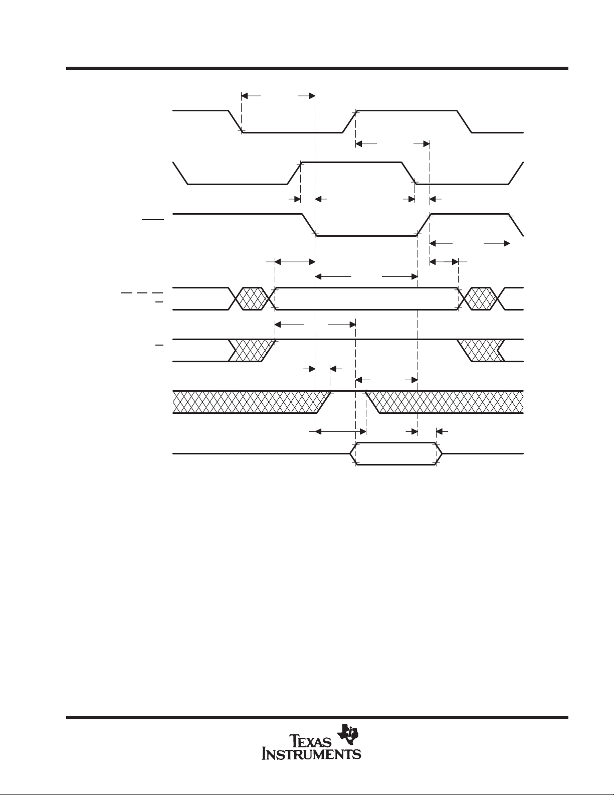
TMS320 SECOND-GENERATION
DEVICES
SPRS010B — MA Y 1987— REVISED NOVEMBER 1990
memory read timing
CLKOUT1
CLKOUT2
t
d(C1-S)
t
d(C1-S)
ADVANCE INFORMATION
STRB
A15-A0,
BR, PS, DS
or IS
R/W
READY
D15-D0
t
su(A)
t
d(C2-S)
t
d(SL-R)
t
h(SL-R)
t
a(A)
t
w(SL)
Valid
t
d(C2-S)
t
su(D)R
Data In
t
w(SH)
t
h(D)R
t
h(A)
42
POST OFFICE BOX 1443 • HOUSTON, TEXAS 77001
Page 43

memory write timing
CLKOUT1
CLKOUT2
STRB
A15-A0,
BR, PS, DS
or IS
t
su(A)
Valid
TMS320 SECOND-GENERATION
DEVICES
SPRS010B — MA Y 1987— REVISED NOVEMBER 1990
t
h(A)
R/W
READY
D15-D0
t
en(D)
t
su(D)W
Data Out
t
dis(D)
t
h(D)W
ADVANCE INFORMATION
POST OFFICE BOX 1443 • HOUSTON, TEXAS 77001
43
Page 44

TMS320 SECOND-GENERATION
DEVICES
SPRS010B — MA Y 1987— REVISED NOVEMBER 1990
one wait-state memory access timing
CLKOUT1
CLKOUT2
STRB
A15-A0, BR,
PS
, DS, R/W or
ADVANCE INFORMATION
IS
READY
t
d(C2H-R)
t
h(C2H-R)
t
h(C2H-R)
Valid
t
d(C2H-R)
D15-D0
(For Read
Operation)
D15-D0
(For Write
Operation)
MSC
t
d(M-R)
t
d(MSC)
t
h(M-R)
t
d(MSC)
t
d(M-R)
Data Out
t
h(M-R)
Data In
44
POST OFFICE BOX 1443 • HOUSTON, TEXAS 77001
Page 45

reset timing
CLKOUT1
RS
A15-A0
D15-D0
t
su(IN)
t
w(RS)
t
d(RS)
t
h(IN)
t
su(IN)
TMS320 SECOND-GENERATION
DEVICES
SPRS010B — MA Y 1987— REVISED NOVEMBER 1990
Valid
Fetch
Location 0
PS
STRB
Control
†
Signals
IACK
Serial Port
†
Control signals are DS
‡
Serial port controls are DX and FSX.
Control
‡
, IS, R/W, and XF.
Valid
Begin
Program
Execution
ADVANCE INFORMATION
POST OFFICE BOX 1443 • HOUSTON, TEXAS 77001
45
Page 46

TMS320 SECOND-GENERATION
DEVICES
SPRS010B — MA Y 1987— REVISED NOVEMBER 1990
interrupt timing (TMS32020)
CLKOUT1
STRB
INT2-INT0
A15-A0
ADVANCE INFORMATION
IACK
interrupt timing (TMS320C25)
CLKOUT1
STRB
t
su(IN)
t
w(IN)
t
f(IN)
FETCH N FETCH N + 1 FETCH I FETCH I + 1
t
d(IACK)
t
su(IN)
t
h(IN)
t
d(IACK)
INT2-INT0
A15-A0
IACK
46
t
h(IN)
t
w(IN)
t
f(IN)
FETCH N FETCH N + 1 FETCH N + 2 N + 3
t
d(IACK)
POST OFFICE BOX 1443 • HOUSTON, TEXAS 77001
t
d(IACK)
FETCH I
Page 47

serial port receive timing
CLKR
FSR
t
su(FS)
DR
t
h(FS)
t
h(DR)
t
t
su(DR)
f(SCK)
TMS320 SECOND-GENERATION
DEVICES
SPRS010B — MA Y 1987— REVISED NOVEMBER 1990
t
c(SCK)
t
r(SCK)
t
w(SCK)
t
w(SCK)
serial port transmit timing
t
CLKX
t
d(CH-DX)
FSX
(Input,
TXM = 0)
t
su(FS)
DX
t
d(CH-FS)
FSX
(Output,
TXM = 1)
w(SCK)
t
h(FS)
t
c(SCK)
t
r(SCK)
t
f(SCK)
t
w(SCK)
t
t
d(FL-DX)
N = 1 N = 8,16
t
d(CH-FS)
d(CH-DX)
ADVANCE INFORMATION
POST OFFICE BOX 1443 • HOUSTON, TEXAS 77001
47
Page 48

TMS32020
SPRS010B — MA Y 1987— REVISED NOVEMBER 1990
BIO timing
CLKOUT1
STRB
FETCH Branch Address FETCH Next Instruction
A15-A0
ADVANCE INFORMATION
external flag timing
CLKOUT1
A15-A0
BIO
STRB
t
su(IN)
FETCH
BIOZ
PC = NPC
t
h(IN)
Valid
Valid
PC = N – 1PC
= N +
1PC
FETCH
SXF/RXF
=
NPC
= N +
2PC
Valid Valid
= N +
1PC
= N +
or Branch Address
t
= N +
3
d(XF)
2
48
XF
Valid
POST OFFICE BOX 1443 • HOUSTON, TEXAS 77001
Page 49

BIO timing
CLKOUT1
STRB
TMS320C25
SPRS010B — MA Y 1987— REVISED NOVEMBER 1990
A15-A0
BIO
external flag timing
CLKOUT1
STRB
t
su(IN)
FETCH Branch Address
FETCH
BIOZ
PC = NPC
t
h(IN)
Valid
= N +
1PC
FETCH Next Instruction
= N +
or Branch Address
2
t
d(XF)
A15-A0
XF
FETCH
SXF/RXF
PC = NPC
POST OFFICE BOX 1443 • HOUSTON, TEXAS 77001
Valid
= N +
1PC
Valid Valid
= N +
2PC
= N +
ADVANCE INFORMATION
3
Valid
49
Page 50

TMS32020
SPRS010B — MA Y 1987— REVISED NOVEMBER 1990
HOLD timing (part A)
CLKOUT1
CLKOUT2
STRB
ADVANCE INFORMATION
HOLD
A15-A0
PS
, DS,
or IS
R/W
D15-D0
HOLDA
FETCH
EXECUTE
t
d(C2H-H)
N N + 1 N + 2
Valid Valid
In In
N N + 1 N/A N/A
N – 1 N Dummy Dead
†
t
dis(C1L-A)
t
dis(AL-A)
t
d(C1L-AL)
†
HOLD
is an asynchronous input and can occur at any time during a clock cycle. If the specified timing is met, the exact sequence shown will occur;
otherwise, a delay of one CLKOUT2 cycle will occur.
50
POST OFFICE BOX 1443 • HOUSTON, TEXAS 77001
Page 51

HOLD timing (part B)
CLKOUT1
CLKOUT2
STRB
TMS32020
SPRS010B — MA Y 1987— REVISED NOVEMBER 1990
t
en(A-C1L)
HOLD
A15-A0
, DS,
PS
or IS
R/W
D15-D0
HOLDA
FETCH
EXECUTE
t
d(C2H-H)
t
d(HH-AH)
N/A N /A N + 2 N + 3
Dead Dead N + 1 N + 2
†
Valid Valid
In In
N + 2 N + 3
ADVANCE INFORMATION
†
HOLD
is an asynchronous input and can occur at any time during a clock cycle. If the specified timing is met, the exact sequence shown will occur;
otherwise, a delay of one CLKOUT2 cycle will occur.
POST OFFICE BOX 1443 • HOUSTON, TEXAS 77001
51
Page 52

TMS320C25
SPRS010B — MA Y 1987— REVISED NOVEMBER 1990
HOLD timing (part A)
CLKOUT1
CLKOUT2
STRB
ADVANCE INFORMATION
HOLD
A15-A0
PS
, DS,
or IS
R/W
D15-D0
HOLDA
FETCH
EXECUTE
t
d(C2H-H)
N N + 1 N + 2
Valid Valid
In In
N N + 1 – –
N – 2 N – 1 N –
†
t
dis(C1L-A)
t
dis(AL-A)
t
d(C1L-AL)
†
is an asynchronous input and can occur at any time during a clock cycle. If the specified timing is met, the exact sequence shown will occur;
HOLD
otherwise, a delay of one CLKOUT2 cycle will occur.
52
POST OFFICE BOX 1443 • HOUSTON, TEXAS 77001
Page 53

HOLD timing (part B)
CLKOUT1
CLKOUT2
STRB
TMS320C25
SPRS010B — MA Y 1987— REVISED NOVEMBER 1990
t
en(A-C1L)
HOLD
PS, DS,
or IS
R/W
D15-D0
HOLDA
A15-A0
FETCH
EXECUTE
t
d(C2H-H)
t
d(HH-AH)
– – – N + 2
– – – N + 1
†
N + 2 N + 2
Valid
In
ADVANCE INFORMATION
†
HOLD
is an asynchronous input and can occur at any time during a clock cycle. If the specified timing is met, the exact sequence shown will occur;
otherwise, a delay of one CLKOUT2 cycle will occur.
POST OFFICE BOX 1443 • HOUSTON, TEXAS 77001
53
Page 54

TMS320 SECOND-GENERATION
DEVICES
SPRS010B — MA Y 1987— REVISED NOVEMBER 1990
TYPICAL SUPPLY CURRENT CHARACTERISTICS FOR TMS320C25
ICC vs f
170
160
150
140
130
120
110
100
90
CC,
80
I mA
70
60
50
40
30
20
10
4 8 12 16 20 24 28 32 36 40 44 48 52
TMS320C25FNL (PLCC) reflow soldering precautions
ADVANCE INFORMATION
Normal Operating Mode
TA = 25°C
f
(CLKIN)
(CLKIN)
and V
, MHz
CC
VCC = 5.50 V
VCC = 5.25 V
VCC = 5.00 V
VCC = 4.75 V
VCC = 4.50 V
Recent tests have identified an industry-wide problem experienced by surface mounted devices exposed to
reflow soldering temperatures. This problem involves a package cracking phenomenon sometimes
experienced by large (e.g., 68-lead) plastic leaded chip carrier (PLCC) packages during surface mount
manufacturing. This phenomenon occur if the TMS320C25FNL is exposed to uncontrolled levels of humidity
prior to reflow solder. This moisture can flash to steam during solder reflow, causing sufficient stress to crack
the package and compromise device integrity. If the TMS320C25FNL is being socketed,
precautions are required. In addition, once the device is soldered into the board, no special handling precautions
are required.
ICC vs f
80
70
60
50
40
CC,
I mA
30
20
10
0
4 8 12 16 20 24 28 32 36 40 44 48 52
Powerdown Mode
f
(CLKIN)
(CLKIN)
and V
, MHz
CC
VCC = 5.50 V
VCC = 5.25 V
VCC = 5.00 V
VCC = 4.75 V
VCC = 4.50 V
no
special handling
In order to minimize moisture absorption, TI ships the TMS320C25FNL in “dry pack” shipping bags with a RH
indicator card and moisture-absorbing desiccant. These moisture-barrier shipping bags will adequately block
moisture transmission to allow shelf storage for 12 months from date of seal when stored at less than 60%
relative humidity (RH) and less than 30°C. Devices may be stored outside the sealed bags indefinitely if stored
at less than 25% RH and 30°C.
Once the bag seal is broken, the devices should be stored at less than 60% RH and 30°C as well as reflow
soldered within two days of removal. In the event that either of the above conditions is not met, TI recommends
these devices be baked in a clean oven at 125°C and 10% maximum RH for 24 hours. This restores the devices
to their “dry packed” moisture level.
NOTE
Shipping tubes will not withstand the 125
°C baking process. Devices should be transferred to a metal tray or tube be-
fore baking. Standard ESD precautions should be followed.
In addition, TI recommends that the reflow process not exceed two solder cycles and the temperature not
exceed 220°C.
If you have any additional questions or concerns, please contact your local TI representative.
54
POST OFFICE BOX 1443 • HOUSTON, TEXAS 77001
Page 55

TMS320 SECOND-GENERATION
SPRS010B — MA Y 1987— REVISED NOVEMBER 1990
MECHANICAL DATA
68-pin GB grid array ceramic package (TMS32020, TMS320C25)
28,448 (1.120)
27,432 (1.080)
DEVICES
Thermal Resistance Characteristics
PARAMETER MAX UNIT
R
R
θJA
θJC
Junction-to-free-air
thermal resistance
Junction-to-case
thermal resistance
3,302 (0.130)
2,794 (0.110)
36 °C/W
6 °C/W
4,953 (0.195)
2,032 (0.080)
0,508 (0.020)
0,406 (0.016)
17,02 (0.670)
Nom
17,02
(0.670)
1,575 (0.062)
1,473 (0.058)
28,448 (1.120)
27,432 (1.080)
Nom
1,397 (0.055)
Max
Dia
2,54
(0.100)
L
K
J
H
G
F
E
D
C
B
A
1234567891011
ALL LINEAR DIMENSIONS ARE IN MILLIMETERS AND PARENTHETICALLY IN INCHES
T.P.
2,54
(0.100)
T.P.
1,27
(0.050)
Nom
ADVANCE INFORMATION
1,524 (0.060)
Nom
4 Places
POST OFFICE BOX 1443 • HOUSTON, TEXAS 77001
55
Page 56

TMS320C25
TMS320C25-50
SPRS010B — MA Y 1987— REVISED NOVEMBER 1990
68-lead plastic leaded chip carrier package (TMS320C25 and TMS320C25-50)
0,25 (0.010) R Max
3 Places
24,33 (0.956)
24,13 (0.950)
(see Note A)
25,27 (0.995)
ADVANCE INFORMATION
25,02 (0.985)
Seating
Plane
(At Seating Plane)
1,27 (0.050) T.P.
(see Note B)
23,62 (0.930)
23,11 (0.910)
Thermal Resistance Characteristics
PARAMETER MAX UNIT
R
R
θJA
θJC
Junction-to-free-air
thermal resistance
Junction-to-case
thermal resistance
ALL LINEAR DIMENSIONS ARE IN MILLIMETERS AND PARENTHETICALLY IN INCHES
1,22 (0.048)
1,07 (0.042)
24,33 (0.956)
24,13 (0.950)
(see Note A)
25,27 (0.995)
25,02 (0.985)
46 °C/W
11 °C/W
× 45°
0,81 (0.032)
0,66 (0.026)
0,51 (0.020)
0,36 (0.014)
Lead Detail
1,35 (0.053)
1,19 (0.047)
2,79 (0.110)
2,41 (0.095)
4,50 (0.177)
4,24 (0.167)
1,52 (0.060)
Min
0,64 (0.025)
Min
0,94 (0.037)
0,69 (0.027)
R
× 45°
NOTES: A. Centerline of center pin, each side, is within 0,10 (0.004) of package centerline as determined by this dimension.
B. Location of each pin is within 0,127 (0.005) of true position with respect to center pin on each side.
WARNING
When reflow soldering is required, refer to page 54 for special handling instructions.
56
POST OFFICE BOX 1443 • HOUSTON, TEXAS 77001
Page 57

TMS320E25
SPRS010B — MA Y 1987— REVISED NOVEMBER 1990
MECHANICAL DATA
68-lead FZ CER-QUAD, ceramic leaded chip carrier package (TMS320E25 only)
This hermetically-sealed chip carrier package consists of a ceramic base, ceramic cap, and a 68-lead frame.
Hermetic sealing is accomplished with glass. The FZ package is intended for both socket- or surface- mounting.
Having a Sn/Pb ratio of 60/40, the tin/lead-coated leads do not require special cleaning or processing
when being surface-mounted.
1,02 (0.040) × 45°
A
(see Note 2)
(see Note 1)
Thermal Resistance Characteristics
PARAMETER
R
θJA
R
θJC
B
Junction-to-free-air
thermal resistance
Junction-to-case
thermal resistance
A
(see Note 2)
B
MAX UNIT
49 °C/W
8 °C/W
0,81 (0.032)
0,66 (0.026)
0,64 (0.025)
R
Max
3 Places
4,57 (0.180)
3,94 (0.155)
3,55 (0.140)
3,05 (0.120)
1,27 (0.050) Typ
(see Note 3)
C
(At Seating
Plane)
0,51 (0.020)
0,36 (0.014)
1,016 (0.040) Min
Ref
3,05 (0.120)
2,29 (0.090)
Seating Plane
(see Note 4)
ADVANCE INFORMATION
JEDEC
OUTLINE
MO-087AA 28
MO-087AB 44
––– 68
NOTES: 1. Glass is optional, and the diameter is dependent on device application.
2. Centerline of center pin, each side, is within 0,10 (0.004) of package centerline as determined by dimension B.
3. Location of each pin is within 0,127 (0.005) of true position with respect to center pin on each side.
4. The lead contact points are within 0,15 (0.006) of being planar.
NO. OF
TERMINALS
(0.485)
(0.685)
(0.985)
ALL LINEAR DIMENSIONS ARE IN MILLIMETERS AND PARENTHETICALLY IN INCHES
A B C
MIN MAX MIN MAX MIN MAX
12,32
17,40
25,02
POST OFFICE BOX 1443 • HOUSTON, TEXAS 77001
12,57
(0.465)
17,65
(0.695)
25,27
(0.995)
10,92
(0.430)
16,00
(0.630)
23,62
(0.930)
11,56
(0.455)
16,64
(0.655)
24,26
(0.955)
10,41
(0.410)
15,49
(0.610)
23,11
(0.910)
10,92
(0.430)
16,00
(0.630)
23,62
(0.930)
57
Page 58

TMS320E25
SPRS010B — MA Y 1987— REVISED NOVEMBER 1990
programming the TMS320E25 EPROM cell
The TMS320E25 includes a 4K × 16-bit EPROM, implemented from an industry-standard EPROM cell, to
perform prototyping and early field testing and to achieve low-volume production. When used with a 4K-word
masked-ROM TMS320C25, the TMS320E25 yields a high-volume, low-cost production as a result of more
migration paths for data. An EPROM adapter socket (part # TMDX3270120), shown in Figure 8, is available to
provide 68-pin to 28-pin conversion for programming the TMS320E25.
ADVANCE INFORMATION
Figure 8. EPROM Adapter Socket
Key features of the EPROM cell include standard programming and verification. For security against copyright
violations, the EPROM cell features an internal protection mechanism to prevent proprietary code from being
read. The protection feature can be used to protect reading the EPROM contents. This section describes
erasure, fast programming and verification, and EPROM protection and verification.
fast programming and verification
The TMS320E25 EPROM cell is programmed using the same family and device codes as the TMS27C64
8K × 8-bit EPROM. The TMS27C64 EPROM series are ultraviolet-light erasable, electrically programmable
read-only memories, fabricated using HVCMOS technology. The TMS27C64 is pin-compatible with existing
28-pin ROMs and EPROMs. The TMS320E25, like the TMS27C64, operates from a single 5-V supply in the
read mode; however, a 12.5-V supply is needed for programming. All programming signals are TTL level. For
programming outside the system, existing EPROM programmers can be used. Locations may be programmed
singly , in blocks, or at random. When programmed in blocks, the data is loaded into the EPROM cell one byte
at a time, the high byte first and the low byte second.
58
POST OFFICE BOX 1443 • HOUSTON, TEXAS 77001
Page 59

TMS320E25
SPRS010B — MA Y 1987— REVISED NOVEMBER 1990
Figure 9 shows the wiring conversion to program the TMS320E25 using the 28-pin pinout of the TMS27C64.
The pin nomenclature table provides a description of the TMS27C64 pins. The code to be programmed into the
device should be serial mode. The TMS320E25 uses 13 address lines to address the 4K-word memory in byte
format.
RS
TMS27C64
V
28
PGM
27
EPT
26
A8
25
A9
24
A11
23
G
22
A10
21
E
20
Q8
19
Q7
18
Q6
17
Q5
16
Q4
15
CC
D7
D6
D5
D4
D3
D2
D1
D0
EPT
V
PP
A0
9876543216867666564636261
10
11
12
13
14
15
16
17
18
19
20
21
E
22
23
24
25
26
27 28 29 30 31 32 33 34 35 36 37 38 39 40 41 42 43
A1A2A3A4A5A6A7
SS
V
8
TMS320E25
68-Pin (FZ)
A8
CC
V
A9
3.9 K
A10
A11
A12
PGM
60
59
58
57
56
55
54
53
CLKIN
52
51
50
49
48
47
46
45
44
G
SIGNALS I/O DEFINITION
A12 (MSB)-A0 (LSB)
CLIN
E
EPT
G
GND
PGM
Q8 (MSB)-Q1 (LSB)
RS
V
CC
V
PP
PP
A7A6A5A4A3A2A1
V
A12
1234567
TMS27C64
A0
8
9
1011121314
Q1Q2Q3
GND
Pin Nomenclature (TMS320E25)
I
I
I
I
I
I
I
I/O
I
I
I
On-chip EPROM programming address lines
Clock oscillator input
EPROM chip select
EPROM test mode select
EPROM read/verify select
Ground
EPROM write/program select
Data lines for byte-wide programming of on-chip 8K bytes of EPROM
Reset for initializing the device
5-V power supply
12.5-V power supply
Figure 9. TMS320E25 EPROM Conversion to TMS27C64 EPROM Pinout
POST OFFICE BOX 1443 • HOUSTON, TEXAS 77001
ADVANCE INFORMATION
59
Page 60

TMS320E25
SPRS010B — MA Y 1987— REVISED NOVEMBER 1990
Table 5 shows the programming levels required for programming, verifying and reading the EPROM cell. The
paragraphs following the table describe the function of each programming level.
Table 5. TMS320E25 Programming Mode Levels
SIGNAL
NAME
PGM 41 27 PULSE V
V
V
V
CLKIN 52 14 V
EPT 24 26 V
ADVANCE INFORMATION
Q1-Q8 18-11 11-13,15-19 D
A12-A10 40-38 2,23,21, ADDR ADDR X ADDR X
A9-A7 37,36,34 24,25,3 ADDR ADDR X ADDR X
A3-A0 30-28,26 7-10 ADDR ADDR X ADDR X
†
In accordance with TMS27C64.
erasure
fast programming
TMS320E25
†
E 22 20 V
G 42 22 V
PP
CC
SS
RS 65 14 V
A6 33 4 ADDR ADDR X ADDR X
A5 32 5 ADDR ADDR X ADDR X
A4 31 3 ADDR ADDR X ADDR X
LEGEND;
VIH = TTL high level; VIL = TTL low level; ADDR = byte address bit
VPP = 12.5 V ± 0.5 V; VCC = 5 ± 0.25 V; X = don’t care
PULSE
Q
OUT
PIN
25 1 V
61,35 28 V
27,44,10 14 V
= low-going TTL level pulse; DIN = byte to be programmed at ADDR
= byte stored at ADDR; RBIT = ROM protect bit.
TMS27C64
PIN
PROGRAM
IL
IH
PP
CC+1
SS
SS
SS
SS
IN
PROGRAM
VERIFY
V
IL
PULSE X PULSE V
IH
V
PP
V
CC+1
V
SS
V
SS
V
SS
V
SS
Q
OUT
PROGRAM
INHIBIT
V
IH
X V
V
PP
V
CC+1
V
SS
V
SS
V
SS
V
SS
HI-Z Q
READ
V
IL
IH
V
CC
V
CC
V
SS
V
SS
V
SS
V
SS
OUT
OUTPUT
DISABLE
V
IL
IH
V
IH
V
CC
V
CC
V
SS
V
SS
V
SS
V
SS
HI-Z
Before programming, the device is erased by exposing the chip through the transparent lid to high-intensity
ultraviolet light (wavelength 2537 Å). The recommended minimum exposure dose (UV-intensity ×
exposure-time) is 15 W•s/cm2. A typical 12 mW/cm2, filterless UV lamp will erase the device in 21 minutes. The
lamp should be located approximately 2.5 cm above the chip during erasure. After erasure, all bits are in the
high state. Note that normal ambient light contains the correct wavelength for erasure. Therefore, when using
the TMS320E25, the window should be covered with an opaque label.
After erasure (all memory bits in the cell are logic one), logic zeroes are programmed into the desired locations.
The fast programming algorithm, shown in Figure 10, is normally used to program the entire EPROM contents,
although individual locations may be programmed separately . A programmed logic zero can be erased only by
ultraviolet light. Data is presented in parallel (eight bits) on pins Q8-Q1. Once addresses and data are stable,
is pulsed. The programming mode is achieved when VPP = 12.5 V , PGM = VIL, VCC = 6 V , G = VIH, and
PGM
E = VIL More than one TMS320E25 can be programmed when the devices are connected in parallel. Locations
can be programmed in any order.
Programming uses two types of programming pulses: prime and final. The length of the prime pulse is 1 ms.
After each prime pulse, the byte being programmed is verified. If correct data is read, the final programming
pulse is applied; if correct data is not read, an additional 1-ms prime pulse is applied up to a maximum of 15
times. The final programming pulse is 4 ms times the number of prime programming pulses applied. This
sequence of programming and verification is performed at V
= 6 V, and VPP = 12.5 V. When the full fast
CC
programming routine is complete, all bits are verified with VCC = VPP = 5 V.
60
POST OFFICE BOX 1443 • HOUSTON, TEXAS 77001
Page 61

TMS320E25
SPRS010B — MA Y 1987— REVISED NOVEMBER 1990
program verify
Programmed bits may be verified with VPP = 12.5 V when G = VIL, E = VIL, and PGM = VIH. Figure 1 1 shows
the timing for the program and verify operation.
Start
Address = First
Location
VCC = 6 ± 0.25 V
VPP = 12.5 V ± 0.25
V
X = 0
Program One
1-ms Pulse
No
Yes Fail
X = 25?
Device
Failed
VCC = VPP = 5 V ± 0.25 V
Fail
Increment X
Verify
One
Byte
Pass
Program One
Pulse of
3X-ms Duration
Last
Address?
Yes
Compare All
Bytes to Original
Data
Pass
No
Increment
Address
ADVANCE INFORMATION
Device
Passed
Figure 10. Fast Programming Flowchart
POST OFFICE BOX 1443 • HOUSTON, TEXAS 77001
61
Page 62

TMS320E25
SPRS010B — MA Y 1987— REVISED NOVEMBER 1990
ADVANCE INFORMATION
A12-A0
Q8-Q1
V
PP
V
CC
PGM
Program
Address Stable Address N + 1
Data In Stable Data Out Valid
E
G
HI-Z
Verify
V
IH
V
IL
VIH/V
VIL/V
V
PP
V
CC
VCC +
V
CC
V
IH
V
IL
V
IH
V
IL
V
IH
V
IL
OH
OL
1
Figure 11. Fast Programming Timing
program inhibit
Programming may be inhibited by maintaining a high level input on the E pin or PGM pin.
read
The EPROM contents may be read independent of the programming cycle, provided the RBIT (ROM protect
bit) has not been programmed. The read is accomplished by setting E to zero and pulsing G low. The contents
of the EPROM location selected by the value on the address inputs appear on Q8-Q1.
output disable
During the EPROM programming process, the EPROM data outputs may be disabled, if desired, by establishing
the output disable state. This state is selected by setting the G
and PGM pins high. While output disable is
selected, Q8-Q1 are placed in the high-impedance state.
ROM protection and verification
This section describes the code protection feature included in the EPROM cell, which protects code against
copyright violations. Table 6 shows the programming levels required for protecting and verifying the EPROM.
The paragraphs following the table describe the protect and verify functions.
62
POST OFFICE BOX 1443 • HOUSTON, TEXAS 77001
Page 63

TMS320E25
SPRS010B — MA Y 1987— REVISED NOVEMBER 1990
Table 6. TMS320E25 Protect and Verify EPROM Mode Levels
SIGNAL
†
In accordance with TMS27C64.
EPROM protect
†
E 22 20 V
G 42 22 V
PGM 41 27 V
V
PP
V
CC
V
SS
CLKIN 52 14 V
RS 65 14 V
EPT 24 26 V
Q8-Q1 18-11 11-13, 15-19 Q8 = PULSE Q8 = RBIT
A12-A10 40-38 2, 23, 21, X X
A9-A7 37, 36, 34 24, 25, 3 X X
A6 33 4 X V
A5 32 5 X X
A4 31 6 V
A3-A0 30-28, 26 7-10 X X
LEGEND;
VIH = TTL high level; VIL = TTL low level; VCC = 5 V ± 0.25 V
VPP = 12.5 V ± 0.5 V; X = don’t care
PULSE
= low-going TTL level pulse; RBIT = ROM protect bit.
TMS320E25 PIN TMS27C64 PIN ROM PROTECT PROTECT VERIFY
V
IL
V
IL
V
IH
V
CC
V
CC
V
SS
V
SS
V
SS
V
PP
IL
X
25 1 V
61,35 28 VCC +
10, 27, 44 14 V
IH
IH
IH
PP
1
SS
SS
SS
PP
IH
The EPROM protect facility is used to completely disable reading of the EPROM contents to guarantee security
of propietary algorithms. This facility is implemented through a unique EPROM cell called the RBIT (EPROM
protect bit) cell. Once the contents to be protected are programmed into the EPROM, the RBIT is programmed,
disabling access to the EPROM contents and disabling the microprocessor mode on the device. Once
programmed, the RBIT can be cleared only by erasing the entire EPROM array with ultraviolet light, thereby
maintaining security of the propietary algorithm. Programming the RBIT is accomplished using the EPROM
protect cycle, which consists of setting the E
, G, PGM, and A4 pins high, VPP and EPT to 2.5 V ± 0.5 V, and
pulsing Q8 low. The complete sequence of operations involved in programming the RBIT is shown in the
flowchart of Figure 12. The required setups in the figure are detailed in Table 6.
ADVANCE INFORMATION
POST OFFICE BOX 1443 • HOUSTON, TEXAS 77001
63
Page 64

TMS320E25
SPRS010B — MA Y 1987— REVISED NOVEMBER 1990
Start
X = 0
Program One
Pulse of 3X-ms
Duration
ADVANCE INFORMATION
Fail
EPROM
Protect
Setup
Program One
1-ms Pulse
X = X + 1
X = 25?
No
Protect
Verify
Setup
Verify
RBIT
Pass
EPROM
Protect
Setup
Yes
Device
Failed
Protect
Verify
Setup
Verify
RBIT
Device
Passed
Figure 12. EPROM Protect Flowchart
protect verify
Protect verify is used following the EPROM protect to verify correct programming of the RBIT (see Figure 12).
When using protect verify , Q8 outputs the state of the RBIT . When RBIT = 1, the EPROM is unprotected; when
RBIT = 0, the EPROM is protected. The EPROM protect and verify timings are shown in Figure 13.
64
POST OFFICE BOX 1443 • HOUSTON, TEXAS 77001
Page 65

TMS320E25
SPRS010B — MA Y 1987— REVISED NOVEMBER 1990
A4
V
PP
V
CC
PGM
Q8
Protect
E
G
HI-Z HI-ZHI-Z
Verify
V
IH
V
IL
V
PP
V
CC
VCC +
V
CC
V
IH
V
IL
V
IH
V
IL
V
IH
V
IL
VIH/V
VIL/V
1
OH
OL
EPT
A6
Figure 13. EPROM Protect Timing
V
PP
V
SS
V
IH
V
IL
ADVANCE INFORMATION
POST OFFICE BOX 1443 • HOUSTON, TEXAS 77001
65
Page 66

TMS320 SECOND-GENERATION
DEVICES
SPRS010B — MA Y 1987— REVISED NOVEMBER 1990
ADVANCE INFORMATION
INDEX
66
POST OFFICE BOX 1443 • HOUSTON, TEXAS 77001
Page 67

NIL
NIL
NIL
SPRS010B — MA Y 1987— REVISED NOVEMBER 1990
accumulator 5. . . . . . . . . . . . . . . . . . . . . . . . . . . . . . .
adapter socket 58. . . . . . . . . . . . . . . . . . . . . . . . . . . .
addressing modes 10. . . . . . . . . . . . . . . . . . . . . . . . .
ALU 5. . . . . . . . . . . . . . . . . . . . . . . . . . . . . . . . . . . . . . .
architecture 5. . . . . . . . . . . . . . . . . . . . . . . . . . . . . . . .
BIT instruction 17. . . . . . . . . . . . . . . . . . . . . . . . . . . . .
block diagram 6. . . . . . . . . . . . . . . . . . . . . . . . . . . . . .
Bulletin board Service 18. . . . . . . . . . . . . . . . . . . . . .
clock
TMS32020 22. . . . . . . . . . . . . . . . . . . . . . . . . . . . .
TMS320C25/E25 28, 29. . . . . . . . . . . . . . . . . . . . .
TMS320C25-50 35, 36. . . . . . . . . . . . . . . . . . . . . .
description 1. . . . . . . . . . . . . . . . . . . . . . . . . . . . . . . . .
development support 18, 19. . . . . . . . . . . . . . . . . . . .
direct addressing 10, 17. . . . . . . . . . . . . . . . . . . . . . .
DMA documentation support 20. . . . . . . . . . . . . . . .
EPROM protection/verification 58-65. . . . . . . . . . . .
external interface 9. . . . . . . . . . . . . . . . . . . . . . . . . . .
flowcharts
EPROM protect 63. . . . . . . . . . . . . . . . . . . . . . . . .
fast 60, 61. . . . . . . . . . . . . . . . . . . . . . . . . . . . . . . . .
hotline 18. . . . . . . . . . . . . . . . . . . . . . . . . . . . . . . . . . . .
immediate addressing 10. . . . . . . . . . . . . . . . . . . . . .
indirect addressing 10, 17. . . . . . . . . . . . . . . . . . . . . .
instruction set 10-16. . . . . . . . . . . . . . . . . . . . . . . . . .
interrupts 9. . . . . . . . . . . . . . . . . . . . . . . . . . . . . . . . . .
introduction 3. . . . . . . . . . . . . . . . . . . . . . . . . . . . . . . .
key features
TMS320 family 1. . . . . . . . . . . . . . . . . . . . . . . . . . .
TMS32020 4. . . . . . . . . . . . . . . . . . . . . . . . . . . . . .
TMS320C25/C25-50/E25 4. . . . . . . . . . . . . . . . . .
microcomputer/microprocessor mode
multiplier 7. . . . . . . . . . . . . . . . . . . . . . . . . . . . . . . . . .
multiprocessing 9. . . . . . . . . . . . . . . . . . . . . . . . . . . . .
operation conditions
TMS32020 17, 21. . . . . . . . . . . . . . . . . . . . . . . . . .
TMS320C25 27. . . . . . . . . . . . . . . . . . . . . . . . . . . .
TMS320C25-50 34. . . . . . . . . . . . . . . . . . . . . . . . .
TMS320E25 27, 33. . . . . . . . . . . . . . . . . . . . . . . . .
overflow 17. . . . . . . . . . . . . . . . . . . . . . . . . . . . . . . . . .
overview
TMS320 5. . . . . . . . . . . . . . . . . . . . . . . . . . . . . . . .
specification 20. . . . . . . . . . . . . . . . . . . . . . . . . . . .
package types 1-5. . . . . . . . . . . . . . . . . . . . . . . . . . . .
pin assignments 2. . . . . . . . . . . . . . . . . . . . . . . . . . . .
pin nomenclature
TMS32020/C25/C25-50 2. . . . . . . . . . . . . . . . . . .
TMS320E25 60. . . . . . . . . . . . . . . . . . . . . . . . . . . .
pinouts
TMS32020/C25/C25-50 1. . . . . . . . . . . . . . . . . . .
TMS320E25 60. . . . . . . . . . . . . . . . . . . . . . . . . . . .
programming levels for EPROM 58-65. . . . . . . . . .
repeat feature 10. . . . . . . . . . . . . . . . . . . . . . . . . . . . .
reflow soldering precaution 54. . . . . . . . . . . . . . . . . .
serial port 7, 9. . . . . . . . . . . . . . . . . . . . . . . . . . . . . . . .
shifter 7. . . . . . . . . . . . . . . . . . . . . . . . . . . . . . . . . . . . .
specification overview 20. . . . . . . . . . . . . . . . . . . . . .
subroutines 9. . . . . . . . . . . . . . . . . . . . . . . . . . . . . . . .
supply current characteristics 54. . . . . . . . . . . . . . . .
switching characteristics
TMS32020 21, 23-26. . . . . . . . . . . . . . . . . . . . . . .
TMS320C25/E25 27, 28-33. . . . . . . . . . . . . . . . . .
TMS320C25-50 34, 35-40. . . . . . . . . . . . . . . . . . .
mechanical data
TMS32020 55. . . . . . . . . . . . . . . . . . . . . . . . . . . . .
TMS320C25 55, 56. . . . . . . . . . . . . . . . . . . . . . . . .
TMS320C25-50 56. . . . . . . . . . . . . . . . . . . . . . . . .
TMS320E25 57. . . . . . . . . . . . . . . . . . . . . . . . . . . .
memory
addressing modes 10, 17. . . . . . . . . . . . . . . . . . . .
control 7. . . . . . . . . . . . . . . . . . . . . . . . . . . . . . . . . .
maps 8. . . . . . . . . . . . . . . . . . . . . . . . . . . . . . . . . . .
POST OFFICE BOX 1443 • HOUSTON, TEXAS 77001
timer 7. . . . . . . . . . . . . . . . . . . . . . . . . . . . . . . . . . . . . .
timing diagrams 41-53, 62, 65. . . . . . . . . . . . . . . . . .
TMS320 Second-Generation 41-47. . . . . . . . . . .
TMS32020 46, 48, 50, 51. . . . . . . . . . . . . . . . . . .
TMS320C25/E25 46, 49, 52, 53. . . . . . . . . . . . . .
TMS3220 product notification 17. . . . . . . . . . . . .
67
Page 68

PACKAGE OPTION ADDENDUM
www.ti.com 4-May-2009
PACKAGING INFORMATION
Orderable Device Status
TMS320C25FNA NRND PLCC FN 68 18 Green (RoHS &
TMS320C25FNAR NRND PLCC FN 68 TBD Call TI Call TI
TMS320C25FNL NRND PLCC FN 68 18 Green (RoHS &
TMS320C25FNL33 OBSOLETE PLCC FN 68 TBD Call TI Call TI
TMS320C25FNLR NRND PLCC FN 68 250 Green (RoHS &
TMS320C25FNLW OBSOLETE PLCC FN 68 Green (RoHS &
TMS320C25GBA NRND CPGA GB 68 21 TBD AU N / A for Pkg Type
TMS320C25GBL NRND CPGA GB 68 21 TBD AU N / A for Pkg Type
TMS320C25PHL NRND QFP PH 80 66 Green (RoHS &
(1)
The marketing status values are defined as follows:
ACTIVE: Product device recommended for new designs.
LIFEBUY: TI has announced that the device will be discontinued, and a lifetime-buy period is in effect.
NRND: Not recommended for new designs. Device is in production to support existing customers, but TI does not recommend using this part in
a new design.
PREVIEW: Device has been announced but is not in production. Samples may or may not be available.
OBSOLETE: TI has discontinued the production of the device.
(2)
Eco Plan - The planned eco-friendly classification: Pb-Free (RoHS), Pb-Free (RoHS Exempt), or Green (RoHS & no Sb/Br) - please check
http://www.ti.com/productcontent for the latest availability information and additional product content details.
TBD: The Pb-Free/Green conversion plan has not been defined.
Pb-Free (RoHS): TI's terms "Lead-Free" or "Pb-Free" mean semiconductor products that are compatible with the current RoHS requirements
for all 6 substances, including the requirement that lead not exceed 0.1% by weight in homogeneous materials. Where designed to be soldered
at high temperatures, TI Pb-Free products are suitable for use in specified lead-free processes.
Pb-Free (RoHS Exempt): This component has a RoHS exemption for either 1) lead-based flip-chip solder bumps used between the die and
package, or 2) lead-based die adhesive used between the die and leadframe. The component is otherwise considered Pb-Free (RoHS
compatible) as defined above.
Green (RoHS & no Sb/Br): TI defines "Green" to mean Pb-Free (RoHS compatible), and free of Bromine (Br) and Antimony (Sb) based flame
retardants (Br or Sb do not exceed 0.1% by weight in homogeneous material)
(1)
Package
Type
Package
Drawing
Pins Package
Qty
Eco Plan
no Sb/Br)
no Sb/Br)
no Sb/Br)
no Sb/Br)
no Sb/Br)
(2)
Lead/Ball Finish MSL Peak Temp
CU NIPDAU Level-3-260C-168 HR
CU NIPDAU Level-3-260C-168 HR
CU NIPDAU Level-3-260C-168 HR
CU NIPDAU Level-3-260C-168 HR
CU NIPDAU Level-4-260C-72 HR
(3)
(3)
MSL, Peak Temp. -- The Moisture Sensitivity Level rating according to the JEDEC industry standard classifications, and peak solder
temperature.
Important Information and Disclaimer:The information provided on this page represents TI's knowledge and belief as of the date that it is
provided. TI bases its knowledge and belief on information provided by third parties, and makes no representation or warranty as to the
accuracy of such information. Efforts are underway to better integrate information from third parties. TI has taken and continues to take
reasonable steps to provide representative and accurate information but may not have conducted destructive testing or chemical analysis on
incoming materials and chemicals. TI and TI suppliers consider certain information to be proprietary, and thus CAS numbers and other limited
information may not be available for release.
In no event shall TI's liability arising out of such information exceed the total purchase price of the TI part(s) at issue in this document sold by TI
to Customer on an annual basis.
OTHER QUALIFIED VERSIONS OF TMS320C25 :
Military: SMJ320C25
•
NOTE: Qualified Version Definitions:
Military - QML certified for Military and Defense Applications
•
Addendum-Page 1
Page 69

IMPORTANT NOTICE
Texas Instruments Incorporated and its subsidiaries (TI) reserve the right to make corrections, modifications, enhancements, improvements,
and other changes to its products and services at any time and to discontinue any product or service without notice. Customers should
obtain the latest relevant information before placing orders and should verify that such information is current and complete. All products are
sold subject to TI’s terms and conditions of sale supplied at the time of order acknowledgment.
TI warrants performance of its hardware products to the specifications applicable at the time of sale in accordance with TI’s standard
warranty. Testing and other quality control techniques are used to the extent TI deems necessary to support this warranty. Except where
mandated by government requirements, testing of all parameters of each product is not necessarily performed.
TI assumes no liability for applications assistance or customer product design. Customers are responsible for their products and
applications using TI components. To minimize the risks associated with customer products and applications, customers should provide
adequate design and operating safeguards.
TI does not warrant or represent that any license, either express or implied, is granted under any TI patent right, copyright, mask work right,
or other TI intellectual property right relating to any combination, machine, or process in which TI products or services are used. Information
published by TI regarding third-party products or services does not constitute a license from TI to use such products or services or a
warranty or endorsement thereof. Use of such information may require a license from a third party under the patents or other intellectual
property of the third party, or a license from TI under the patents or other intellectual property of TI.
Reproduction of TI information in TI data books or data sheets is permissible only if reproduction is without alteration and is accompanied
by all associated warranties, conditions, limitations, and notices. Reproduction of this information with alteration is an unfair and deceptive
business practice. TI is not responsible or liable for such altered documentation. Information of third parties may be subject to additional
restrictions.
Resale of TI products or services with statements different from or beyond the parameters stated by TI for that product or service voids all
express and any implied warranties for the associated TI product or service and is an unfair and deceptive business practice. TI is not
responsible or liable for any such statements.
TI products are not authorized for use in safety-critical applications (such as life support) where a failure of the TI product would reasonably
be expected to cause severe personal injury or death, unless officers of the parties have executed an agreement specifically governing
such use. Buyers represent that they have all necessary expertise in the safety and regulatory ramifications of their applications, and
acknowledge and agree that they are solely responsible for all legal, regulatory and safety-related requirements concerning their products
and any use of TI products in such safety-critical applications, notwithstanding any applications-related information or support that may be
provided by TI. Further, Buyers must fully indemnify TI and its representatives against any damages arising out of the use of TI products in
such safety-critical applications.
TI products are neither designed nor intended for use in military/aerospace applications or environments unless the TI products are
specifically designated by TI as military-grade or "enhanced plastic." Only products designated by TI as military-grade meet military
specifications. Buyers acknowledge and agree that any such use of TI products which TI has not designated as military-grade is solely at
the Buyer's risk, and that they are solely responsible for compliance with all legal and regulatory requirements in connection with such use.
TI products are neither designed nor intended for use in automotive applications or environments unless the specific TI products are
designated by TI as compliant with ISO/TS 16949 requirements. Buyers acknowledge and agree that, if they use any non-designated
products in automotive applications, TI will not be responsible for any failure to meet such requirements.
Following are URLs where you can obtain information on other Texas Instruments products and application solutions:
Products Applications
Amplifiers amplifier.ti.com Audio www.ti.com/audio
Data Converters dataconverter.ti.com Automotive www.ti.com/automotive
DLP® Products www.dlp.com Broadband www.ti.com/broadband
DSP dsp.ti.com Digital Control www.ti.com/digitalcontrol
Clocks and Timers www.ti.com/clocks Medical www.ti.com/medical
Interface interface.ti.com Military www.ti.com/military
Logic logic.ti.com Optical Networking www.ti.com/opticalnetwork
Power Mgmt power.ti.com Security www.ti.com/security
Microcontrollers microcontroller.ti.com Telephony www.ti.com/telephony
RFID www.ti-rfid.com Video & Imaging www.ti.com/video
RF/IF and ZigBee® Solutions www.ti.com/lprf Wireless www.ti.com/wireless
Mailing Address: Texas Instruments, Post Office Box 655303, Dallas, Texas 75265
Copyright © 2009, Texas Instruments Incorporated
 Loading...