

x
Ǹ
TMP320C40KGDC, SMJ320C40KGDC, TMP320C40KGDCT, SMJ320C40KGDCT
FLOATING-POINT DIGITAL SIGNAL PROCESSOR
KNOWN GOOD DIES
SGUS024B – MARCH 1997 – REVISED APRIL 2000
1
POST OFFICE BOX 1443 • HOUSTON, TEXAS 77251–1443
D
SMJ: QML Processing to MIL–PRF–38535
D
TMP: Commercial Level Processing
D
Operating Temperature Ranges:
– Military (M) –55°C to 125°C
– Commercial (C) –25°C to 85°C
– Commercial (L) 0°C to 70°C
D
Highest Performance Floating-Point Digital
Signal Processor (DSP)
– ’C40-50:
40-ns Instruction Cycle Time:
50 MFLOPS, 25 MIPS, 275 MOPS,
320 MBps
– ’C40-40:
50-ns Instruction Cycle Time:
40 MFLOPS, 20 MIPS, 220 MOPS,
256 MBps
D
Six Communications Ports
D
6-Channel Direct Memory Access (DMA)
Coprocessor
D
Single-Cycle Conversion to and From
IEEE-745 Floating-Point Format
D
Single Cycle 1/x, 1/
D
Source-Code Compatible With SMJ320C30
D
Validated Ada Compiler
D
Single-Cycle 40-Bit Floating-Point,
32-Bit Integer Multipliers
D
12 40-Bit Registers, 8 Auxiliary Registers,
14 Control Registers, and 2 Timers
D
IEEE Standard 1149.1† Test-Access Port
(JTAG)
D
Two Identical External Data and Address
Buses Supporting Shared Memory Systems
and High Data-Rate, Single-Cycle
Transfers:
– High Port-Data Rate of 100 MBytes/s
(Each Bus)
– 16G-Byte Continuous
Program/Data/Peripheral Address Space
– Memory-Access Request for Fast,
Intelligent Bus Arbitration
– Separate Address-, Data-, and
Control-Enable Pins
– Four Sets of Memory-Control Signals
Support Different Speed Memories in
Hardware
D
Fabricated Using 0.72-µm Enhanced
Performance Implanted CMOS (EPIC)
Technology by Texas Instruments (TI)
D
Separate Internal Program, Data, and DMA
Coprocessor Buses for Support of Massive
Concurrent Input/Output (I/O) of Program
and Data Throughput, Maximizing
Sustained Central Processing Unit (CPU)
Performance
D
On-Chip Program Cache and
Dual-Access/Single-Cycle RAM for
Increased Memory-Access Performance
– 512-Byte Instruction Cache
– 8K Bytes of Single-Cycle Dual-Access
Program or Data RAM
– ROM-Based Bootloader Supports
Program Bootup Using 8-, 16-, or 32-Bit
Memories Over Any One of the
Communications Ports
description
The TMP/SMJ320C40KGD DSP is a 32-bit, floating-point processor manufactured in 0.72-µm, double-level
metal CMOS technology . It is the fourth generation of DSPs from Texas Instruments, and it is the world’ s first
DSP designed for parallel processing. The on-chip parallel processing capabilities of the ’C40 make the
floating-point performance required by many applications achievable and cost-effective.
The TMP/SMJ320C40 is the first DSP with on-chip communication ports for processor-to-processor
communication using simple communication software with no external hardware. This allows connectivity with
no external glue logic. The communication ports remove I/O bottlenecks, and the independent smart-DMA
coprocessor is able to handle the CPU I/O requirements.
Please be aware that an important notice concerning availability, standard warranty, and use in critical applications of
Texas Instruments semiconductor products and disclaimers thereto appears at the end of this data sheet.
PRODUCTION DATA information is current as of publication date.
Products conform to specifications per the terms of Texas Instruments
standard warranty. Production processing does not necessarily include
testing of all parameters.
Copyright 2000, Texas Instruments Incorporated
†
IEEE Standard 1149.1–1990 Standard Test-Access Port and Boundary-Scan Architecture
EPIC and TI are trademarks of Texas Instruments Incorporated.
On products compliant to MIL-PRF-38535, all parameters are tested
unless otherwise noted. On all other products, production
processing does not necessarily include testing of all parameters.
TMP320C40KGDC, SMJ320C40KGDC, TMP320C40KGDCT, SMJ320C40KGDCT
FLOATING-POINT DIGITAL SIGNAL PROCESSOR
KNOWN GOOD DIES
SGUS024B – MARCH 1997 – REVISED APRIL 2000
2
POST OFFICE BOX 1443 • HOUSTON, TEXAS 77251–1443
description (continued)
The features of the communication ports are:
D
Six communication ports for direct interprocessor communication and processor I/O
D
20 MBps bidirectional interface on each communication port for high-speed and low-cost multiprocessor
interface
D
Separate input and output first-in, first-out (FIFO) buffers for I/O and processor-to-processor
communication
D
Automatic arbitration and handshaking for direct processor-to-processor connection
The DMA coprocessor allows concurrent I/O and CPU processing for superior sustained CPU performance.
The key features of the DMA coprocessor:
D
Link pointers that allow DMA channels to auto-initialize
D
Parallel CPU operation and DMA transfers
D
Six DMA channels support communication-port-to-memory data transfers
The TMP/SMJ320C40KGD CPU is configured for high-speed internal parallel processing. The key features of
the CPU are:
D
Eight operations/cycles
– 40-/32-bit floating-point/integer multiply
– 40-/32-bit floating-point/integer arithmetic and logic unit (ALU) operation
– Two data accesses
– Two address-register updates
D
IEEE floating-point conversion
D
Division and square-root support
D
’C30 assembly language compatibility
D
Byte and halfword accessibility
Key factors in a parallel-processing implementation are the development tools that are available. The ’C40 is
supported by a host of parallel-processing development tools for developing and simulating code and for
debugging parallel-processing systems. The code generation tools include:
D
Optimizing ANSI C compiler with a runtime library that supports use of communication ports and DMA
D
SPOX, by Spectron Microsystems Incorporated, which provides parallel processing support as well as
DMA and communication port drivers
D
Assembler and linker with support for mapping program and data to parallel processors.
SPOX is a trademark of Spectron Microsystems, Inc.

TMP320C40KGDC, SMJ320C40KGDC, TMP320C40KGDCT, SMJ320C40KGDCT
FLOATING-POINT DIGITAL SIGNAL PROCESSOR
KNOWN GOOD DIES
SGUS024B – MARCH 1997 – REVISED APRIL 2000
3
POST OFFICE BOX 1443 • HOUSTON, TEXAS 77251–1443
description (continued)
The simulation tools include:
D
Parallel DSP system-level simulation, by Logic Modeling Corporation (LMC), which includes a hardware
verification (HV) model and a full functional (FF) model
D
TI software simulator with high-level language debugger interface for simulating a single processor
The hardware development and verification tools include:
D
Parallel processor in-circuit emulator and high-level language debugger: XDS510
D
Parallel processor development system with four TMS320C40s, local and global memory, and
communication port connections
known good die technology
Known good die (KGD) options are offered for use in multichip modules and chip-on-board (COB) applications.
There are currently two verification technologies used at TI to support KGD requirements for the
TMP/SMJ320C40KGD: Removable Tab (R-Tab), and Temporary Wire Bond (TWB).
The availability of selected DSP products in a tape-automated bond (T AB) configuration has made possible the
use of a removable T AB technique. The TAB leadframe is attached to a gold-bumped die using modified bonding
parameters. This technique allows easy removal of the tape after all needed 100% screens and parametric tests
have been performed. The tape is removed from the tested part and the die is shipped in a conventional die
container. The gold bumps remain on the bond pads, which allow for subsequent attachment of gold-ball bonds.
Similarly , with KGD using the TWB technique, bond wires are attached to the bond pads using adjusted bonding
parameters which allow for easy removal of the die after all needed 100% screens and parametric tests have
been performed. The die is removed from the temporary package and the die is shipped in a conventional die
container.
visual inspection of known good die (KGD) using temporary wire bond (TWB) process
QML KGD devices produced using the TWB technology do not optically meet MIL-STD-883E (Method 2010,
paragraph 3.1.1.1.h) metal bond pad visual inspection criterion due to the bond pad marks formed during
bonding removal process. However, these devices have been reliably bonded using normal wire bond
precesses, and pass bond strength evaluations.
electrical specifications
For military electrical and timing specifications, please refer to the
SMJ320C40 Digital Signal Processor
data
sheet, literature number SGUS017. For commercial electrical and timing specifications, see the
TMS320C40
Digital Signal Processor Data Sheet
, literature number SPRS038.
XDS510 is a trademark of Texas Instruments Incorporated.
TMP320C40KGDC, SMJ320C40KGDC, TMP320C40KGDCT, SMJ320C40KGDCT
FLOATING-POINT DIGITAL SIGNAL PROCESSOR
KNOWN GOOD DIES
SGUS024B – MARCH 1997 – REVISED APRIL 2000
4
POST OFFICE BOX 1443 • HOUSTON, TEXAS 77251–1443
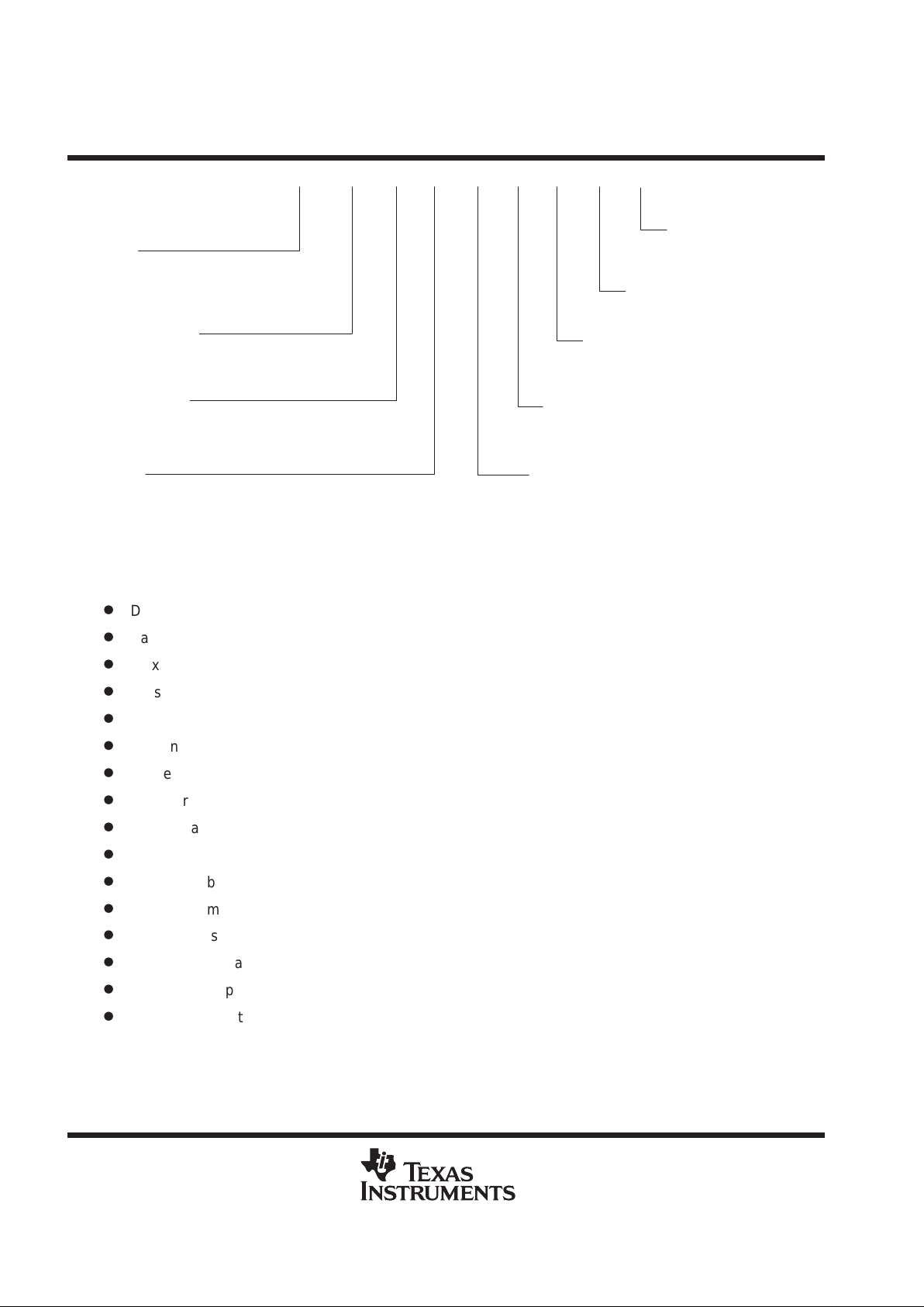
SMJ 320 C 40 MKGD 50
PREFIX
SMJ = MIL-PRF-38535 Processing
TMP = Commercial Level
DEVICE FAMILY
320 = DSP Family
TECHNOLOGY
C = CMOS
DEVICE
40 = Floating-Point DSP
SPEED RANGE
40 = 40 MHz
50 = 50 MHz
PACKAGE TYPE
KGD = Known Good Die
TEMPERATURE RANGE
M (Military) = –55°C to 125°C
L (Commercial) = 0°Cto70°C
C
DIE REVISION
C = Revision 5.2
T
KGD OPTION
T = TWB process
blank = R-T ab process
Figure 1. TMP/SMJ320C40KGD Device Nomenclature
JEDEC STANDARD
D
Die thickness is approximately 15 mils ± 1 mil.
D
Backside surface finish is silicon.
D
Maximum allowable die junction operating temperature is 175°C.
D
Glassivation material is compressive nitride.
D
Bond pad metal is composed of copper-doped aluminum.
D
Percent defective allowed for burned-in die is 5.
D
Life test data is available.
D
Configuration control notification.
D
Group A attribute summary is available (SMJ only).
D
Suggested die-attach material is silver glass (QMI 2569F).
D
Suggested bond wire size is 1.25 mil.
D
For gold bumped KGD die, suggested bonding method is gold-ball bonding.
D
ESD rating is Class II.
D
Maximum allowable peak process temperature for die-attach is 440°C ± 5°C (for QMS2569F)
D
Saw kerf is dependent on blade size used.
D
Die backside potential is left floating.

TMP320C40KGDC, SMJ320C40KGDC, TMP320C40KGDCT, SMJ320C40KGDCT
FLOATING-POINT DIGITAL SIGNAL PROCESSOR
KNOWN GOOD DIES
SGUS024B – MARCH 1997 – REVISED APRIL 2000
5
POST OFFICE BOX 1443 • HOUSTON, TEXAS 77251–1443
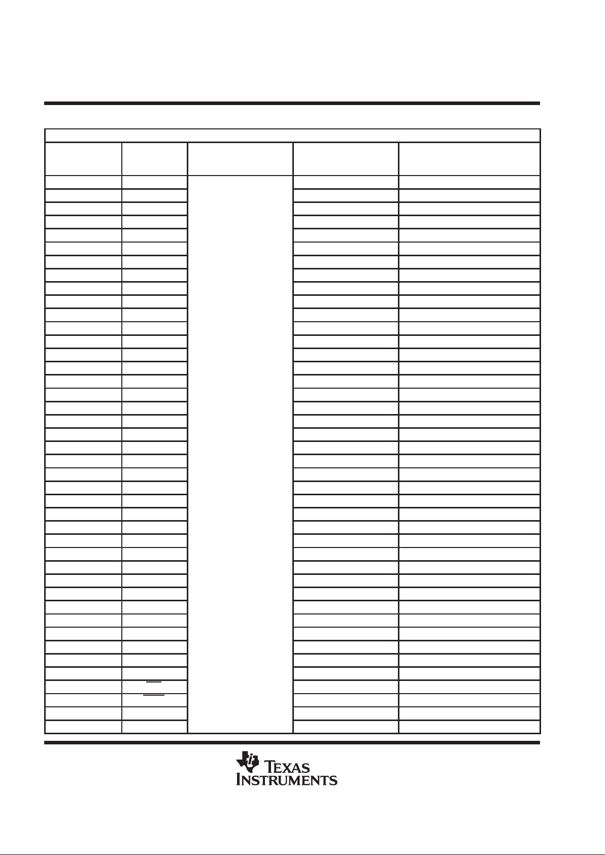
’320C40 (rev 5.2) known good die pad information
325 244Die Side Number 4
Pad Number One 1
•
•
•
Die Side Number 1
•
•
•
81
Zero-Zero
(origin)
82 162Die Side Number 2
243
•
•
•
Die Side Number 3
•
•
•
163
Die Designator
Figure 2. ’320C40 Die Numbering Format
(See Table 1)
Table 1 provides a reference for the following:
D
The ’C40 signal identities in relation to the pad numbers
D
The ’C40 X,Y coordinates, where bond pad 82 serves as the origin (0,0)
In addition, the following notes are significant:
A. X,Y coordinate data is in microns.
B. The active silicon dimensions are 12424.86 µm × 12035.52 µm (489.16 mils × 473.83 mils).
C. The die size is approximately 12598.40 µm × 12192.00 µm (496.00 mils × 480.00 mils).
D. Bond pad dimensions are 108.00 µm × 108.00 µm (4.25 mils × 4.25 mils).
E. Center of bond pad to edge of die min (without scribe) = 107.80 µm (4.24 mils).
F. For R-Tab devices, gold bump dimensions are approximately 92 µm × 92 µm (3.62 mils × 3.62 mils).
G. Coordinate origin is at (0,0) (center of bond pad 82).
TMP320C40KGDC, SMJ320C40KGDC, TMP320C40KGDCT, SMJ320C40KGDCT
FLOATING-POINT DIGITAL SIGNAL PROCESSOR
KNOWN GOOD DIES
SGUS024B – MARCH 1997 – REVISED APRIL 2000
6
POST OFFICE BOX 1443 • HOUSTON, TEXAS 77251–1443
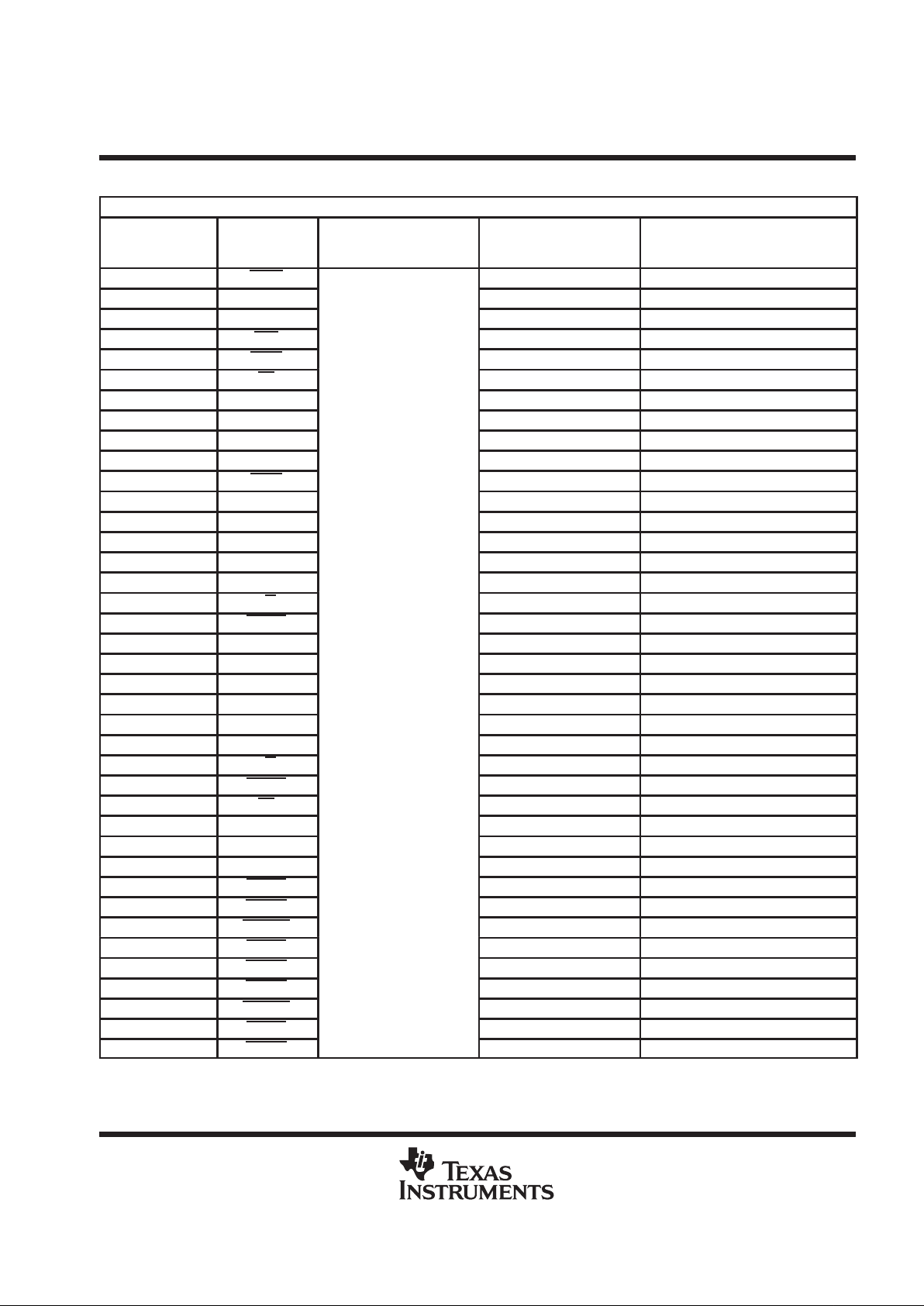
Table 1. ’320C40 Die Pad/TAB Lead Information : Rev. 5.2 (0,72 µm)
DIE SIDE #1
C40 DIE BOND
PAD LOCATIONS
DIE/TAB BOND
PAD IDENTITY
X-COORDINATE OF DIE
BOND PAD
Y-COORDINATE OF DIE
BOND PAD
PITCH OF LEAD
(#, #) REFERENCES WHICH DIE
BOND PADS
1 D31 11368.44 126.00 (1, 2)
2 D30 11242.44 126.00 (2, 3)
3 D29 11116.44 126.00 (3, 4)
4 D28 10990.44 126.00 (4, 5)
5 D27 10864.44 126.00 (5, 6)
6 D26 10738.44 126.00 (6, 7)
7 GDDV
DD
10612.44 126.00 (7, 8)
8 D25 10486.44 126.00 (8, 9)
9 D24 10360.44 126.00 (9, 10)
10 D23 10234.44 126.00 (10, 11)
11 D22 10108.44 126.00 (11, 12)
12 D21 9982.44 126.00 (12, 13)
13 D20 9856.44 126.00 (13, 14)
14 D19 9730.44 126.00 (14, 15)
15 D18 9604.44 126.00 (15, 16)
16 D17 9478.44 126.00 (16, 17)
17 D16 9352.44 126.00 (17, 18)
18 CV
SS
9226.44 126.00 (18, 19)
19 IV
SS
9100.44 126.00 (19, 20)
20 GDDV
DD
8974.44 126.00 (20, 21)
21 D
VSS
8848.44 126.00 (21, 22)
22 D15
–
429.48
8722.44 126.00 (22, 23)
23 D14 8596.44 126.00 (23, 24)
24 D13 8470.44 126.00 (24, 25)
25 D12 8344.44 126.00 (25, 26)
26 D11 8218.44 126.00 (26, 27)
27 D10 8092.44 126.00 (27, 28)
28 D9 7966.44 126.00 (28, 29)
29 D8 7840.44 126.00 (29, 30)
30 D7 7714.44 126.00 (30, 31)
31 D6 7588.44 126.00 (31, 32)
32 D5 7462.44 126.00 (32, 33)
33 GDDV
DD
7336.44 126.00 (33, 34)
34 D4 7210.44 126.00 (34, 35)
35 D3 7084.44 126.00 (35, 36)
36 D2 6958.44 126.00 (36, 37)
37 D1 6832.44 126.00 (37, 38)
38 D0 6706.44 156.42 (38, 39)
39 CE1 6550.02 172.80 (39, 40)
40 RDY1 6377.22 152.10 (40, 41)
41 DV
SS
6225.12 126.00 (41, 42)
42 CV
SS
6099.12 126.00 (42, 43)
TMP320C40KGDC, SMJ320C40KGDC, TMP320C40KGDCT, SMJ320C40KGDCT
FLOATING-POINT DIGITAL SIGNAL PROCESSOR
KNOWN GOOD DIES
SGUS024B – MARCH 1997 – REVISED APRIL 2000
7
POST OFFICE BOX 1443 • HOUSTON, TEXAS 77251–1443
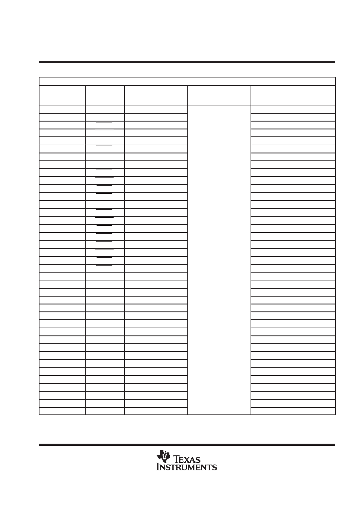
Table 1. ’320C40 Die Pad/TAB Lead Information : Rev. 5.2 (0,72 µm) (Continued)
DIE SIDE #1 (CONTINUED)
C40 DIE BOND
PAD LOCATIONS
DIE/TAB BOND
PAD IDENTITY
X-COORDINATE OF DIE
BOND PAD
Y-COORDINATE OF DIE
BOND PAD
PITCH OF LEAD
(#, #) REFERENCES WHICH DIE
BOND PADS
43 LOCK 5973.12 126.00 (43, 44)
44 V
DDL
5847.12 126.00 (44, 45)
45 V
SSL
5721.12 156.42 (45, 46)
46 CE0 5564.70 172.80 (46, 47)
47 RDY0 5391.90 172.80 (47, 48)
48 DE 5219.10 172.80 (48, 49)
49 TCK 5046.30 152.10 (49, 50)
50 TDO 4894.20 156.42 (50, 51)
51 TDI 4737.78 172.80 (51, 52)
52 TMS 4564.98 172.80 (52, 53)
53 TRST 4392.18 151.10 (53, 54)
54 EMU0 4240.08 126.00 (54, 55)
55 EMU1 4114.08 126.00 (55, 56)
56 DV
SS
3988.08 126.00 (56, 57)
57 DV
DD
3962.08 126.00 (57, 58)
58 PAGE1 3736.08 126.00 (58, 59)
59 R/W1 3610.08 126.00 (59, 60)
60 STRB1 3484.08 126.00 (60, 61)
61 STAT0 3358.08 126.00 (61, 62)
62 STAT1
– 429.48
3232.08 126.00 (62, 63)
63 IV
SS
3106.08 126.00 (63, 64)
64 STAT2 2980.08 126.00 (64, 65)
65 STAT3 2854.08 127.44 (65, 66)
66 PAGE0 2726.64 126.00 (66, 67)
67 R/W0 2600.64 126.00 (67, 68)
68 STRB0 2474.64 156.42 (68, 69)
69 AE 2318.22 174.24 (69, 70)
70 RESETLOC 1 2143.98 152.10 (70, 71)
71 DV
DD
1991.88 156.42 (71, 72)
72 RESETLOC 0 1835.46 172.80 (72, 73)
73 RESET 1662.66 172.80 (73, 74)
74 CRDY5 1510.56 126.00 (74, 75)
75 CSTRB5 1384.56 126.00 (75, 76)
76 CACK5 1258.56 126.00 (76, 77)
77 CREQ5 1132.56 126.00 (77, 78)
78 CRDY4 1006.56 126.00 (78, 79)
79 CSTRB4 880.56 126.00 (79, 80)
80 CACK4 754.56 126.00 (80, 81)
81 CREQ4 628.56

TMP320C40KGDC, SMJ320C40KGDC, TMP320C40KGDCT, SMJ320C40KGDCT
FLOATING-POINT DIGITAL SIGNAL PROCESSOR
KNOWN GOOD DIES
SGUS024B – MARCH 1997 – REVISED APRIL 2000
8
POST OFFICE BOX 1443 • HOUSTON, TEXAS 77251–1443
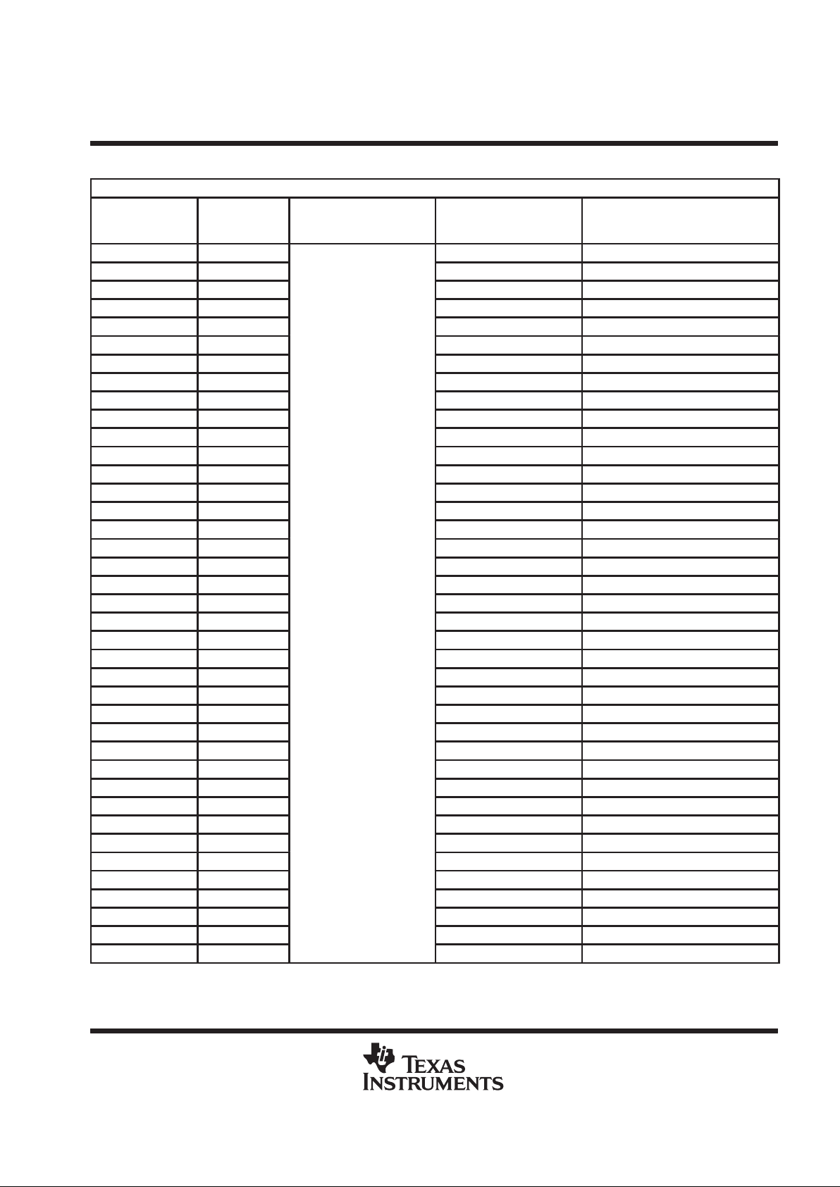
Table 1. ’320C40 Die Pad/TAB Lead Information : Rev. 5.2 (0,72 µm) (Continued)
DIE SIDE #2
C40 DIE BOND
PAD LOCATIONS
DIE/TAB BOND
PAD IDENTITY
X-COORDINATE OF DIE
BOND PAD
Y-COORDINATE OF DIE
BOND PAD
PITCH OF LEAD
(#, #) REFERENCES WHICH DIE
BOND PADS
82 CV
SS
0.00 1062.00 (82, 83)
83 DV
SS
1062.00 126.00 (83, 84)
84 DV
DD
1188.00 126.00 (84, 85)
85 C5D7 1314.00 126.00 (85, 86)
86 C5D6 1440.00 126.00 (86, 87)
87 C5D5 1566.00 126.00 (87, 88)
88 C5D4 1692.00 126.00 (88, 89)
89 C5D3 1818.00 126.00 (89, 90)
90 C5D2 1944.00 126.00 (90, 91)
91 C5D1 2070.00 126.00 (91, 92)
92 C5D0 2196.00 126.00 (92, 93)
93 DV
DD
2322.00 126.00 (93, 94)
94 C4D7 2448.00 126.00 (94, 95)
95 C4D6 2574.00 126.00 (95, 96)
96 C4D5 2700.00 126.00 (96, 97)
97 C4D4 2813.40 126.00 (97, 98)
98 C4D3 2952.00 126.00 (98, 99)
99 C4D2 3078.00 126.00 (99, 100)
100 C4D1 3204.00 126.00 (100, 101)
101 C4D0 3330.00 126.00 (101, 102)
102 CV
SS
3456.00
126.00 (102, 103)
103 DV
SS
3582.00
0.00
126.00 (103, 104)
104 DV
DD
3708.00 126.00 (104, 105)
105 C3D7 3834.00 126.00 (105, 106)
106 C3D6 3960.00 126.00 (106, 107)
107 C3D5 4086.00 126.00 (107, 108)
108 C3D4 4212.00 126.00 (108, 109)
109 C3D3 4338.00 126.00 (109, 110)
110 C3D2 4464.00 126.00 (110, 111)
111 C3D1 4590.00 126.00 (111, 112)
112 C3D0 4716.00 126.00 (1 12, 113)
113 DV
DD
4842.00 126.00 (113, 114)
114 IV
SS
4968.00 126.00 (114, 115)
115 C2D7 5094.00 126.00 (1 15, 116)
116 C2D6 5220.00 126.00 (1 16, 117)
117 C2D5 5346.00 126.00 (1 17, 118)
118 C2D4 5472.00 126.00 (1 18, 119)
119 C2D3 5598.00 126.00 (119, 120)
120 C2D2 5724.00 126.00 (120, 121)
121 C2D1 5850.00 126.00 (121, 122)
122 C2D0 5976.00 126.00 (122, 123)
123 CV
SS
6102.00 126.00 (123, 124)
TMP320C40KGDC, SMJ320C40KGDC, TMP320C40KGDCT, SMJ320C40KGDCT
FLOATING-POINT DIGITAL SIGNAL PROCESSOR
KNOWN GOOD DIES
SGUS024B – MARCH 1997 – REVISED APRIL 2000
9
POST OFFICE BOX 1443 • HOUSTON, TEXAS 77251–1443
Table 1. ’320C40 Die Pad/TAB Lead Information : Rev. 5.2 (0,72 µm) (Continued)
DIE SIDE #2 (CONTINUED)
C40 DIE BOND
PAD LOCATIONS
DIE/TAB BOND
PAD IDENTITY
X-COORDINATE OF DIE
BOND PAD
Y-COORDINATE OF DIE
BOND PAD
PITCH OF LEAD
(#, #) REFERENCES WHICH DIE
BOND PADS
124 DV
SS
6228.00 126.00 (124, 125)
125 DV
DD
6354.00 126.00 (125, 126)
126 CRDY3 6480.00 126.00 (126, 127)
127 CSTRB3 6606.00 126.00 (127, 128)
128 CACK3 6732.00 126.00 (128, 129)
129 CREQ3 6858.00 126.00 (129, 130)
130 V
DDL
6984.00 126.00 (130, 131)
131 V
SSL
7110.00 126.00 (131, 132)
132 CRDY2 7236.00 126.00 (132, 133)
133 CSTRB2 7362.00 126.00 (133, 134)
134 CACK2 7488.00 126.00 (134, 135)
135 CREQ2 7614.00 126.00 (135, 136)
136 DV
DD
7740.00 126.00 (136, 137)
137 CRDY1 7866.00 126.00 (137, 138)
138 CSTRB1 7992.00 126.00 (138, 139)
139 CACK1 8118.00 126.00 (139, 140)
140 CREQ1 8244.00 126.00 (140, 141)
141 CRDY0 8370.00 126.00 (141, 142)
142 CSTRB0 8496.00 126.00 (142, 143)
143 CACK0 8622.00
0.00
126.00 (143, 144)
144 CREQ0 8748.00 126.00 (144, 145)
145 CV
SS
8874.00 126.00 (145, 146)
146 DV
SS
9000.00 126.00 (146, 147)
147 IV
SS
9126.00 126.00 (147, 148)
148 DV
DD
9252.00 126.00 (148, 149)
149 C1D7 9378.00 126.00 (149, 150)
150 C1D6 9504.00 126.00 (150, 151)
151 C1D5 9630.00 126.00 (151, 152)
152 C1D4 9756.00 126.00 (152, 153)
153 C1D3 9882.00 126.00 (153, 154)
154 C1D2 10008.00 126.00 (154, 155)
155 C1D1 10134.00 126.00 (155, 156)
156 C1D0 10260.00 126.00 (156, 157)
157 DV
DD
10386.00 126.00 (157, 158)
158 C0D7 10512.00 126.00 (158, 159)
159 C0D6 10638.00 126.00 (159, 160)
160 C0D5 10764.00 126.00 (160, 161)
161 C0D4 10890.00 126.00 (161, 162)
162 C0D3 11016.00

TMP320C40KGDC, SMJ320C40KGDC, TMP320C40KGDCT, SMJ320C40KGDCT
FLOATING-POINT DIGITAL SIGNAL PROCESSOR
KNOWN GOOD DIES
SGUS024B – MARCH 1997 – REVISED APRIL 2000
10
POST OFFICE BOX 1443 • HOUSTON, TEXAS 77251–1443
Table 1. ’320C40 Die Pad/TAB Lead Information : Rev. 5.2 (0,72 µm) (Continued)
DIE SIDE #3
C40 DIE BOND
PAD LOCATIONS
DIE/TAB BOND
PAD IDENTITY
X-COORDINATE OF DIE
BOND PAD
Y-COORDINATE OF DIE
BOND PAD
PITCH OF LEAD
(#, #) REFERENCES WHICH DIE
BOND PADS
163 C0D2 810.00 126.00 (163, 164)
164 C0D1 936.00 126.00 (164, 165)
165 C0D0 1062.00 126.00 (165, 166)
166 CV
SS
1188.00 126.00 (166, 167)
167 DV
DD
1314.00 156.42 (167, 168)
168 ROMEN 1470.42 152.46 (168, 169)
169 IIOF0 1622.88 126.00 (169, 170)
170 DV
SS
1748.88 126.00 (170, 171)
171 IIOF1 1874.88 126.00 (171, 172)
172 IIOF2 2000.88 126.00 (172, 173)
173 IIOF3 2126.88 156.42 (173, 174)
174 NMI 2283.30 152.10 (174, 175)
175 LSTRB0 2435.40 126.00 (175, 176)
176 LR/W0 2561.40 126.00 (176, 177)
177 LP AGE0 2687.40 156.42 (177, 178)
178 LRDY0 2843.82 172.80 (178, 179)
179 LCE0 3016.62 152.10 (179, 180)
180 LSTRB1 3168.72 126.00 (180, 181)
181 LR/W1 3294.72 126.00 (181, 182)
182 DV
DD
3420.72 126.00 (182, 183)
183 CV
SS
3546.72 126.00 (183, 184)
184 LP AGE1
11779.74
3672.72 156.42 (184, 185)
185 LRDY1 3829.14 172.80 (185, 186)
186 LCE1 4001.94 172.80 (186, 187)
187 LDE 4174.74 152.10 (187, 188)
188 TCLK0 4326.84 126.00 (188, 189)
189 TCLK1 4452.84 126.00 (189, 190)
190 H3 4578.84 126.00 (190, 191)
191 H1 4704.84 156.42 (191, 192)
192 LAE 4861.26 152.10 (192, 193)
193 IV
SS
5013.36 126.00 (193, 194)
194 LLOCK 5139.36 126.00 (194, 195)
195 LSTAT0 5265.36 126.00 (195, 196)
196 LSTAT1 5391.36 126.00 (196, 197)
197 LSTAT2 5517.36 126.00 (197, 198)
198 LSTAT3 5643.36 127.44 (198, 199)
199 IACK 5770.80 126.00 (199, 200)
200 V
DDL
5896.80 126.00 (200, 201)
201 V
SSL
6022.80 131.94 (201, 202)
202 X1 6154.74 171.58 (202, 203)
203 X2/CLKIN 6326.28 168.12 (203, 204)
204 CV
SS
6494.40 126.00 (204, 205)
TMP320C40KGDC, SMJ320C40KGDC, TMP320C40KGDCT, SMJ320C40KGDCT
FLOATING-POINT DIGITAL SIGNAL PROCESSOR
KNOWN GOOD DIES
SGUS024B – MARCH 1997 – REVISED APRIL 2000
11
POST OFFICE BOX 1443 • HOUSTON, TEXAS 77251–1443
Table 1. ’320C40 Die Pad/TAB Lead Information : Rev. 5.2 (0,72 µm) (Continued)
DIE SIDE #3 (CONTINUED)
C40 DIE BOND
PAD LOCATIONS
DIE/TAB BOND
PAD IDENTITY
X-COORDINATE OF DIE
BOND PAD
Y-COORDINATE OF DIE
BOND PAD
PITCH OF LEAD
(#, #) REFERENCES WHICH DIE
BOND PADS
205 DV
DD
6620.40 126.00 (205, 206)
206 DV
SS
6746.40 127.44 (206, 207)
207 LA30 6873.84 126.00 (207, 208)
208 LA29 6999.84 126.00 (208, 209)
209 LA28 7125.84 126.00 (209, 210)
210 LA27 7251.84 126.00 (210, 211)
211 LADV
DD
7377.84 126.00 (211, 212)
212 LA26 7503.84 126.00 (212, 213)
213 LA25 7629.84 126.00 (213, 214)
214 LA24 7755.84 126.00 (214, 215)
215 LA23 7881.84 126.00 (215, 216)
216 LA22 8007.84 126.00 (216, 217)
217 LA21 8133.84 126.00 (217, 218)
218 LA20 8259.84 126.00 (218, 219)
219 LA19 8385.84 126.00 (219, 220)
220 LA18 8511.84 126.00 (220, 221)
221 LA17 8637.84 126.00 (221, 222)
222 LA16 8763.84 126.00 (222, 223)
223 LADV
DD
8889.84 126.00 (223, 224)
224 CV
SS
11779.74
9015.84 126.00 (224, 225)
225 DV
SS
9141.84 126.00 (225, 226)
226 LA15 9267.84 126.00 (226, 227)
227 LA14 9393.84 126.00 (227, 228)
228 LA13 9519.84 126.00 (228, 229)
229 LA12 9645.84 126.00 (229, 230)
230 LA11 9771.84 126.00 (230, 231)
231 LA10 9897.84 126.00 (231, 232)
232 LA9 10023.84 126.00 (232, 233)
233 LA8 10149.84 126.00 (233, 234)
234 LA7 10275.84 126.00 (234, 235)
235 LA6 10401.84 126.00 (235, 236)
236 LA5 10527.84 126.00 (236, 237)
237 LA4 10653.84 126.00 (237, 238)
238 LADV
DD
10779.84 126.00 (238, 239)
239 LA3 10905.84 126.00 (239, 240)
240 LA2 11031.84 126.00 (240, 241)
241 LA1 11157.84 126.00 (241, 242)
242 LA0 11283.84 205.92 (242, 243)
243 DV
SS
11489.76

TMP320C40KGDC, SMJ320C40KGDC, TMP320C40KGDCT, SMJ320C40KGDCT
FLOATING-POINT DIGITAL SIGNAL PROCESSOR
KNOWN GOOD DIES
SGUS024B – MARCH 1997 – REVISED APRIL 2000
12
POST OFFICE BOX 1443 • HOUSTON, TEXAS 77251–1443
Table 1. ’320C40 Die Pad/TAB Lead Information : Rev. 5.2 (0,72 µm) (Continued)
DIE SIDE #4
C40 DIE BOND
PAD LOCATIONS
DIE/TAB BOND
PAD IDENTITY
X-COORDINATE OF DIE
BOND PAD
Y-COORDINATE OF DIE
BOND PAD
PITCH OF LEAD
(#, #) REFERENCES WHICH DIE
BOND PADS
244 CV
SS
10953.72 126.00 (244, 245)
245 LD31 10827.72 126.00 (245, 246)
246 LD30 10701.72 126.00 (246, 247)
247 LD29 10575.72 126.00 (247, 248)
248 LD28 10449.72 126.00 (248, 249)
249 LDDV
DD
10323.72 126.00 (249, 250)
250 LD27 10197.72 126.00 (250, 251)
251 LD26 10071.72 126.00 (251, 252)
252 LD25 9945.72 126.00 (252, 253)
253 LD24 9819.72 126.00 (253, 254)
254 LD23 9693.72 126.00 (254, 255)
255 LD22 9567.72 126.00 (255, 256)
256 LD21 9441.72 126.00 (256, 257)
257 LD20 9315.72 126.00 (257, 258)
258 LD19 9189.72 126.00 (258, 259)
259 LD18 9063.72 126.00 (259, 260)
260 LD17 8937.72 126.00 (260, 261)
261 LDDV
DD
8811.72 126.00 (261, 262)
262 CV
SS
8685.72 126.00 (262, 263)
263 DV
SS
8559.72 126.00 (263, 264)
264 IV
SS
8433.72
126.00 (264, 265)
265 LD16 8307.72
11819.88
126.00 (265, 266)
266 LD15 8181.72 126.00 (266, 267)
267 LD14 8055.72 126.00 (267, 268)
268 LD13 7929.72 126.00 (268, 269)
269 LD12 7803.72 126.00 (269, 270)
270 LD11 7677.72 126.00 (270, 271)
271 LD10 7551.72 126.00 (271, 272)
272 LD9 7425.72 126.00 (272, 273)
273 LD8 7299.72 126.00 (273, 274)
274 LD7 7173.72 126.00 (274, 275)
275 LD6 7047.72 126.00 (275, 276)
276 LD5 6921.72 126.00 (276, 277)
277 LDDV
DD
6795.72 126.00 (277, 278)
278 LD4 6669.72 126.00 (278, 279)
279 LD3 6543.72 126.00 (279, 280)
280 LD2 6417.72 126.00 (280, 281)
281 LD1 6291.72 126.00 (281, 282)
282 LD0 6165.72 127.62 (282, 283)
283 V
DDL
6038.10 126.00 (283, 284)
284 V
SSL
5912.10 126.00 (284, 285)
285 CV
SS
5786.10 126.00 (285, 286)

TMP320C40KGDC, SMJ320C40KGDC, TMP320C40KGDCT, SMJ320C40KGDCT
FLOATING-POINT DIGITAL SIGNAL PROCESSOR
KNOWN GOOD DIES
SGUS024B – MARCH 1997 – REVISED APRIL 2000
13
POST OFFICE BOX 1443 • HOUSTON, TEXAS 77251–1443
Table 1. ’320C40 Die Pad/TAB Lead Information : Rev. 5.2 (0,72 µm) (Continued)
DIE SIDE #4 (CONTINUED)
C40 DIE BOND
PAD LOCATIONS
DIE/TAB BOND
PAD IDENTITY
X-COORDINATE OF DIE
BOND PAD
Y-COORDINATE OF DIE
BOND PAD
PITCH OF LEAD
(#, #) REFERENCES WHICH DIE
BOND PADS
286 DV
SS
5660.10 126.00 (286, 287)
287 A30 5534.10 126.00 (287, 288)
288 A29 5408.10 126.00 (288, 289)
289 A28 5282.10 126.00 (289, 290)
290 GADV
DD
5156.10 126.00 (290, 291)
291 A27 5030.10 126.00 (291, 292)
292 A26 4904.10 126.00 (292, 293)
293 A25 4778.10 126.00 (293, 294)
294 A24 4652.10 126.00 (294, 295)
295 A23 4526.10 126.00 (295, 296)
296 A22 4400.10 126.00 (296, 297)
297 A21 4274.10 126.00 (297, 298)
298 A20 4148.10 126.00 (298, 299)
299 A19 4022.10 126.00 (299, 300)
300 A18 3896.10 126.00 (300, 301)
301 A17 3770.10 126.00 (301, 302)
302 GADV
DD
3644.10 126.00 (302, 303)
303 CV
SS
3518.10 126.00 (303, 304)
304 DV
SS
3392.10 126.00 (304, 305)
305 A16 3266.10
126.00 (305, 306)
306 A15 3140.10
11819.88
126.00 (306, 307)
307 A14 3014.10 126.00 (307, 308)
308 A13 2888.10 126.00 (308, 309)
309 A12 2762.10 126.00 (309, 310)
310 A11 2636.10 126.00 (310, 311)
311 A10 2510.10 126.00 (311, 312)
312 A9 2384.10 126.00 (312, 313)
313 A8 2258.10 126.00 (313, 314)
314 A7 2132.10 126.00 (314, 315)
315 A6 2006.10 126.00 (315, 316)
316 A5 1880.10 126.00 (316, 317)
317 A4 1754.10 126.00 (317, 318)
318 GADV
DD
1628.10 126.00 (318, 319)
319 A3 1502.10 126.00 (319, 320)
320 A2 1376.10 126.00 (320, 321)
321 A1 1250.10 126.00 (321, 322)
322 A0 1124.10 126.00 (322, 323)
323 CV
SS
998.10 558.00 (323, 324)
324 DV
SS
440.10 630.00 (324, 325)
325 SUBS – 189.90

IMPORTANT NOTICE
T exas Instruments and its subsidiaries (TI) reserve the right to make changes to their products or to discontinue
any product or service without notice, and advise customers to obtain the latest version of relevant information
to verify, before placing orders, that information being relied on is current and complete. All products are sold
subject to the terms and conditions of sale supplied at the time of order acknowledgment, including those
pertaining to warranty, patent infringement, and limitation of liability.
TI warrants performance of its semiconductor products to the specifications applicable at the time of sale in
accordance with TI’s standard warranty. Testing and other quality control techniques are utilized to the extent
TI deems necessary to support this warranty. Specific testing of all parameters of each device is not necessarily
performed, except those mandated by government requirements.
Customers are responsible for their applications using TI components.
In order to minimize risks associated with the customer’s applications, adequate design and operating
safeguards must be provided by the customer to minimize inherent or procedural hazards.
TI assumes no liability for applications assistance or customer product design. TI does not warrant or represent
that any license, either express or implied, is granted under any patent right, copyright, mask work right, or other
intellectual property right of TI covering or relating to any combination, machine, or process in which such
semiconductor products or services might be or are used. TI’s publication of information regarding any third
party’s products or services does not constitute TI’s approval, warranty or endorsement thereof.
Copyright 2000, Texas Instruments Incorporated
 Loading...