

Page 1

Please be aware that an important notice concerning availability, standard warranty, and use in critical applications of Texas Instruments
查询TMP141供应商
TMP141
SBAS347 − MARCH 2005
Digital Out Temperature Sensor with
Single-Wire SensorPath Bus
FEATURES
D SensorPath INTERFACE
D FOUR ADDRESSES
D RESOLUTION: +0.25°C (10-bit)
D WIDE TEMPERATURE RANGE:
−40°C to +125°C
D LOW QUIESCENT CURRENT: 110µA (typ)
D TEMPERATURE ACCURACY: ±2°C (max)
D EXTENDED SUPPLY RANGE: +2.7V to +5.5V
D MICRO-SIZE PACKAGES:
SOT23-6 or MSOP-8
APPLICATIONS
D MOTHERBOARDS
D VIDEO CARDS
D BASE STATIONS
D ROUTERS
Temperature
DESCRIPTION
The TMP141 is a digital output temperature sensor that
utilizes the single-wire SensorPath interface. The TMP141
is capable of measuring temperatures within 2°C of
accuracy over a temperature range of −25°C to +85°C and
3°C of accuracy over −40°C to +125°C. Low supply
current, and a supply range from 2.7V to 5.5V, make the
TMP141 an excellent candidate for a wide range of
low-power applications. The TMP141 is available in
SOT23-6 and MSOP-8 packages.
The TMP141 provides a simple, low-cost way to do
temperature measurement/monitoring and is ideal as a
part of an overall hardware health monitoring system. Up
to four TMP141s can be attached to a SensorPath bus. A
master configures the TMP141s and reads the
temperature output from all devices. No external sensing
components are needed for the TMP141 to measure and
report temperature.
Diode
Temp.
Sensor
V+
GND
semiconductor products and disclaimers thereto appears at the end of this data sheet.
SensorPath is a trademark of National Semiconductor. All other trademarks are the property of their respective owners.
! !
∆Σ
A/D
Converter
OSC
TMP141
www.ti.com
Control
Logic
Serial
Interface
Config.
and Temp.
Register
ADD0
ADD1
SWD
Copyright 2005, Texas Instruments Incorporated
Page 2

"#$#
TMP141
SOT23-6
DBV
−40°C to +125°C
T141
TMP141
MSOP-8
DGK
−40°C to +125°C
T14G
SBAS347 − MARCH 2005
www.ti.com
ABSOLUTE MAXIMUM RATINGS
(1)
Supply Voltage +7V. . . . . . . . . . . . . . . . . . . . . . . . . . . . . . . . . . . . . . .
Signal Input Terminals, Voltage
Signal Input Terminals, Current
(2)
(V−) −0.5V to (V+) + 0.5V. . . .
(2)
10mA. . . . . . . . . . . . . . . . . . . . .
Maximum Output Current (SWD low) 10mA. . . . . . . . . . . . . . . . . . .
Operating Temperature −55°C to +127°C. . . . . . . . . . . . . . . . . . . . .
Storage Temperature −60°C to +150°C. . . . . . . . . . . . . . . . . . . . . . .
proper handling and installation procedures can cause damage.
ESD damage can range from subtle performance degradation to
complete device failure. Precision integrated circuits may be more
susceptible t o damage because very small parametric changes could
cause the device not to meet its published specifications.
This integrated circuit can be damaged by ESD. Texas
Instruments recommends that all integrated circuits be
handled with appropriate precautions. Failure to observe
Junction Temperature +150°C. . . . . . . . . . . . . . . . . . . . . . . . . . . . . . .
Lead Temperature (infrared 15s, vapor 60s) +300°C. . . . . . . . . . . .
ESD Rating:
Human Body Model (HBM) 4000V. . . . . . . . . . . . . . . . . . . . . . .
Charged-Device Model 1000V. . . . . . . . . . . . . . . . . . . . . . . . . .
(1)
Stresses above these ratings may cause permanent damage.
Exposure to absolute maximum conditions for extended periods
may degrade device reliability. These are stress ratings only , an d
functional operation of the device at these or any other conditions
beyond those specified is not supported.
(2)
Input terminals should not be driven beyond the power-supply
rails. Input signals that can swing more than 0.5V beyond the
supply rails should be current-limited to 10mA or less.
ORDERING INFORMATION
PRODUCT PACKAGE-LEAD
(1)
PACKAGE
DESIGNATOR
SPECIFIED
TEMPERATURE
RANGE
PACKAGE
MARKING
ORDERING
NUMBER
TRANSPORT
MEDIA, QUANTITY
TMP141AIDBVT Tape and Reel, 250
TMP141AIDBVR Tape and Reel, 3000
TMP141AIDGKT Tape and Reel, 250
TMP141AIDGKR Tape and Reel, 3000
(1)
For the most current package and ordering information, see the Package Option Addendum at the end of this document, or see the TI web site
at www .ti.com.
PIN CONFIGURATIONS
Top View
1
ADD0
2
GND
(1)
3
NC
NOTE: Pin 1 is determined by orienting the package marking as indicated in the diagram.
(1) NC = no connection. NC pins must be tied to ground.
2
T141
SOT23−6
1
6
ADD1
5
SWD
4
V+
NC
NC
NC
V+
(1)
(1)
(1)
T14G
2
3
4
MSOP−8
8
SWD
7
ADD1
6
ADD0
5
GND
Page 3

"#$#
www.ti.com
SBAS347 − MARCH 2005
ELECTRICAL CHARACTERISTICS
At TA = −40°C to +125°C and VS = +3.0V to +3.6V , unless otherwise noted.
PARAMETER CONDITIONS MIN TYP MAX UNIT
TEMPERATURE INPUT
Range −40 +125 °C
Error T
ERROR
T = −25°C to +85°C ±0.2 ±2 °C
T = −40°C to +125°C ±3 °C
vs Supply ±0.2 ±0.5 °C/V
Resolution 10 Bits
Default Conversion Time t
CONV
See Table 4 for conversion time settings. 162 190 218 ms
DIGIT AL INPUT/OUTPUT PINS (SWD and ADD pins)
Input/Output Capacitance C
IN/OUT
SWD PIN
Input Leakage Current I
Input Logic Level Voltage (High) V
L
I
L
IH
GND < VIN < 5.5V and VS = GND/OPEN 0.005 µA
VS = 2.7V to 5.5V 0.6 × V
Input Logic Level Voltage (Low) V
IL
VS = 2.7V to 5.5V −0.5 0.25 × V
Input Hysteresis V
Output Logic Level Voltage (Low) V
Output OFF Current I
HYST
OL
OH
ADD0 and ADD1 PINS
Input Leakage Current I
Input Logic Level Voltage (High) V
Input Logic Level Voltage (Low) V
L
IH
IL
SensorPath CHARACTERISTICS
SWD Fall Time t
SWD Rise Time t
Min. Inactive Time Between SWD Signals t
Master or TMP141 Reset Drive Time t
TMP141 Detects Bus Activity t
f
r
INACT
RST
SFEdet
R
PULL-UP
R
PULL-UP
= 1.25kΩ ± 30%, CL = 400pF 300 ns
= 1.25kΩ ± 30%, CL = 400pF 1000 ns
Bus at High Level 11 µs
Master Drive Time
Data Bit 0 Write, Data Bit 0 Read t
Data Bit 1 Write t
Start Bit t
Mtr0
Mtr1
MtrS
TMP141 Drive Time
Data Bit 0−1 Read t
Attention Request t
Reset t
SLout1
SLoutA
RST_MA X
After VS is Above 2.6V 95 500 ms
POWER SUPPLY
Specified Voltage Range 3.0 3.6 V
Operating Voltage Range 2.7 5.5 V
Quiescent Current I
Q
While Converting
Power-On Reset Voltage 1.5 2.6 V
TEMPERATURE RANGE
Specified Range −40 +125 °C
Operating Range −55 +127 °C
Storage Range −60 +150 °C
Thermal Resistance q
JA
MSOP-8 150 °C/W
SOT23-6 200 °C/W
(1)
SensorPath activity only has a slight effect on quiescent current.
TMP141
0.25 °C
3 pF
GND < VIN < V
S
0.005 10 µA
2.1 VS + 0.5 V
S
VS + 0.5 V
−0.5 0.8 V
300 mV
S
IOL = 4mA 0.4 V
IOL = 50µA 0.2 V
0.005 10 µA
GND < VIN < V
S
0.9 × V
−0.5 0.1 × V
0.005 10 µA
S
VS + 0.5 V
S
354 µs
9.6 µs
11.8 17 µs
35.4 48.9 µs
80 109 µs
28.3 38.3 µs
165 228 µs
Standby 80 120 µA
(1)
110 170 µA
V
V
3
Page 4

"#$#
SBAS347 − MARCH 2005
TYPICAL CHARACTERISTICS
At TA = −40°C to +125°C and VS = +3.0V to +3.6V , unless otherwise noted.
200
180
160
140
A)
µ
120
(
Q
I
100
80
60
40
QUIESCENT CURRENT vsTEMPERATURE
5.5V
3.3V
2.7V
−55−35−
155 25456585105125
Temperature (_C)
200
180
160
140
A)
µ
(
120
STBY
I
100
80
60
40
2.7V
−55−35−
www.ti.com
I
vs TEMPERATURE
STBY
5.5V
3.3V
155 25456585105125
Temperature (_C)
1.0
0.8
0.6
0.4
C)
_
0.2
Error (
0
−
0.2
−
0.4
−
0.6
TYPICAL PERFORMANCE FOR THREE UNITS
−55−35−
155 25456585105125
Temperature (_C)
120
110
100
A)
µ
90
(
Q
I
80
220
210
200
190
180
170
Conversion Time −Default Setting (ms)
160
QUIESCENT CURRENT vs CONVERSION TIME
Peak Current
Average Current
TYPICAL CONVERSION TIME vs TEMPERATURE
−55−35−
3.3V
155 25456585105125
Temperature (_C)
2.7V
5.5V
70
60
0 200 400 600 800 1000 1200 1400 1600
Conversion Time (ms)
4
Page 5
www.ti.com
"#$#
SBAS347 − MARCH 2005
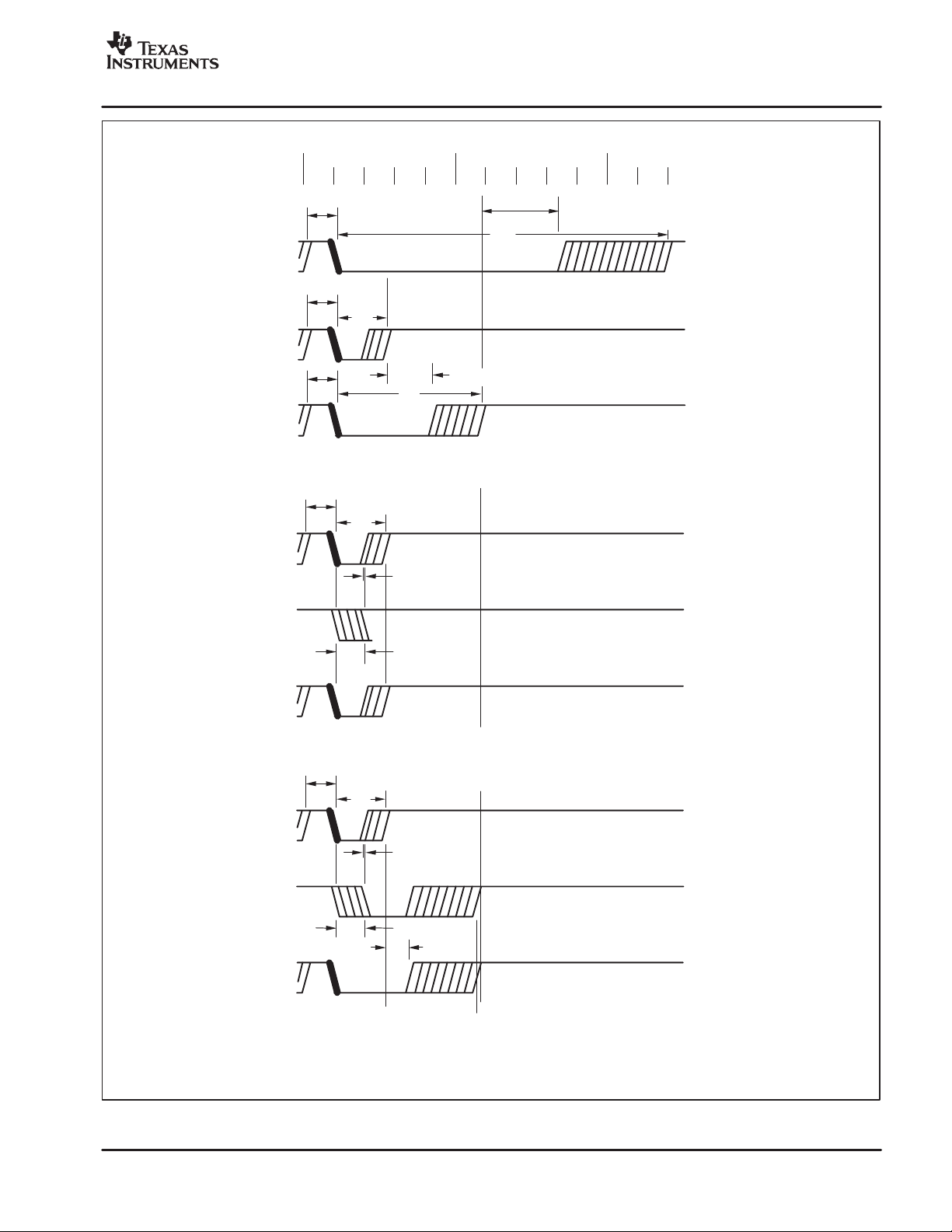
0µs50
t
INACT
t
INACT
t
Mtr0
µ
s 100µs
DetectStart
t
MtrS
Master Write Start
Master Write 0
t
INACT
t
Mtr1
SlvDetectData1
Master Write 1
1a: Master Write timing and slave detection of the data placed on the SWD bus by the master .
t
INACT
t
Mtr0
Masterstartsa bit
SlvDetect_st
(1)
Slave detects bus activity and
doesnothing,leaving the bit a 0.
t
SFEdet
Master Read 0
1b: To place a ‘0’ on the bus, the slave does not drive the bus.
t
INACT
t
Mtr0
Master starts a bit
SlvDetect_st
(1)
Slave pulls Bus low to send back a 1
t
SFEdet
MstDetect_1
Master Read 1
1c: To place a ‘1’ on the bus, the slave holds the bus low after detecting that the master has started a data bit.
NOTE: (1) Margin from t
SFEdet
to t
Mtr0
is 2.2µs.
Figure 1. TMP141 Read and Write Signal Timing
5
Page 6
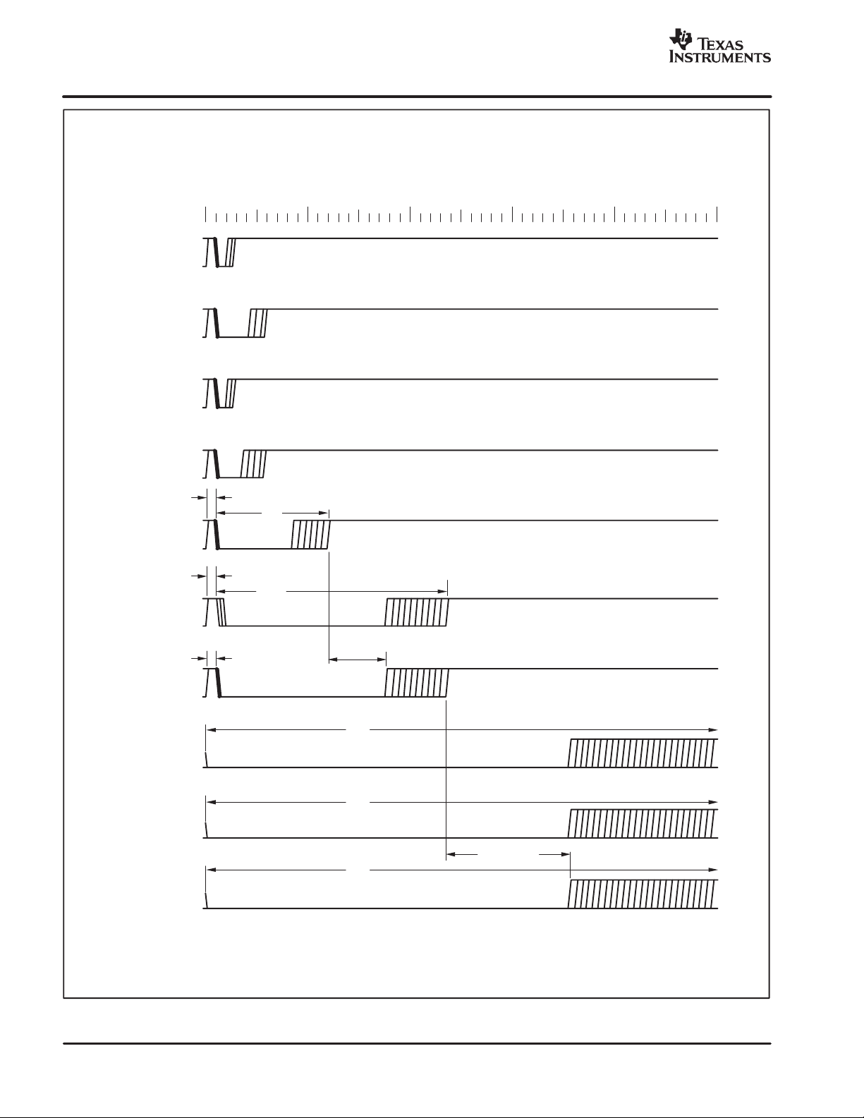
"#$#
SBAS347 − MARCH 2005
www.ti.com
Master Write 0
Master Write 1
Master Read 0
Master Read 1
Master Write Start
Sout_Attention
0µs50
µ
s 100µs150µs 200µs250µs300µs 350µs 400µs450µs
t
INACT
t
MtrS
t
INACT
t
SLoutA
Attention
Mout_Reset
Sout_Reset
Reset
Attention
t
INACT
Detect
t
RST
t
RST
Reset Detect
t
RST
Figure 2. Relationship of the Five Types of Signals on SWD
6
Page 7

www.ti.com
"#$#
SBAS347 − MARCH 2005
OVERVIEW
The TMP141 is a digital output temperature sensor that
uses the single-wire SensorPath interface protocol. It does
not require any external sensing components for
measuring temperature. In order to minimize circuit board
space, the TMP141 is offered in the MSOP-8 and
SOT23-6 packages.
The primary usage of SensorPath-based systems is for
systems that monitor hardware health. The predefined
SensorPath functions are: temperature measurement,
voltage measurement, and non-volatile memory. The
specification allows for expansion by defining new
functions or enlarging upon the predefined functions. The
TMP141 implements the temperature measurement
function with a resolution of 0.25°C.
The SensorPath interface allows a master to read up to
seven slave devices on a bus, four of which can be
TMP141s. The master interrogates devices on the bus to
determine what they are, their capabilities, and how they
can be used. Devices on the Single-Wire Data (SWD) bus
are open drain. Therefore, the SWD bus requires a 1.25kΩ
pull-up resistor on the bus. This resistor may be provided
by the master. If the pull-up resistor is not included within
the master, an external resistor must be attached to the
bus. A 0.1µF capacitor is recommended for power-supply
bypassing, as shown in Figure 3. Registers inside each
device include information that identifies the device
capabilities, manufacturer, part ID, and even device
revision number.
VS=3.3V
TEMPERATURE SENSING AND
CONVERSION
The TMP141 senses the absolute temperature by utilizing
a diode which is part of the IC. Therefore, the sensing
device of the TMP141 is the chip itself. Thermal paths run
through the package leads as well as the plastic package,
and the lower thermal resistance of metal causes the leads
to provide the primary thermal path.
To maintain accuracy in applications that require air or
surface temperature measurement, care should be taken
that the package and leads thermally connect with the
surface where the temperature measurement is desired.
For example, a thermally-conductive adhesive assists in
achieving accurate surface temperature measurements.
Even without special precautions, because of the very low
power consumption of the TMP141, self-heating will
normally be well below 1LSB (0.25°C).
TYPICAL APPLICATION
The TMP141 is normally used with the address pins wired
high or low to select one of four possible addresses. The
value read from the hardware pins plus one is stored in
register 0 as the device number. When the master
transmits a matching device number, the TMP141 will
respond. In the example shown in Figure 3, ADD1:ADD0
are wired to 2h. In this example, 3h will be stored in register
0. When the master addresses device number 3, the
TMP141 in Figure 3 will respond. The TMP141 will also
work well in applications where ADD0:ADD1 are driven by
logic levels since it reads these pins every time it does a
conversion or bus transaction (see Table 2).
0.1µF
ADD1
TMP141 Master
ADD0
V
SS
Optional
Ω
R = 1.25k
SWD
The resistor R may be
integratedinto the master.
Figure 3. Typical Connections of the TMP141
7
Page 8

"#$#
SBAS347 − MARCH 2005
www.ti.com
DIGITAL INTERFACE
Up to four TMP141 devices can be connected to a single
signaling line, which is called Single-Wire Data (SWD).
This line is similar to the data line (SMBDAT) of the
industry-standard SMBus. The SensorPath bus uses a
power supply of 3.3V; therefore, the signaling levels are
approximately 3.3V and 0V.
Data is encoded in a pulse width encoding scheme. All
signaling is done by pulling the bus low for varying lengths
of time. With the exception of Reset and Attention
Request, the master starts all bits. Thus, when sending
data, the TMP141 does not pull the bus low. Rather, when
the TMP141 needs to send a ‘1’, it first detects that the line
has been pulled low by the master, and then holds the line
low long enough to signal a ‘1’. To send a ‘0’, the TMP141
simply leaves the bus alone; the master has already
placed a ‘0’ on the bus.
The SWD interface used on the TMP141 has five types of
signals that are identified by the length of time that the line
is held low. Conceptually, this device operates as a
five-state signaling system. The more common signals
have shorter durations in order to speed overall
transmission. The five signals and their approximate times
are:
D Data 0: Transmit a ‘0’ bit (15µs)
D Data 1: Transmit a ‘1’ bit (42µs)
D Start: Used by the master at the beginning of a
transaction (95µs)
D Attention Request: May be used by the TMP141 to
request service (196µs)
D Reset: Must be asserted by both the master and
slave(s) after power up. It may be asserted at other
times as needed (at least 348µs).
The bus must be inactive for at least 11µs before any
signal.
Attention Request
Any slave device may signal an Attention Request. Before
sending an Attention Request, the slave monitors the bus
to ensure that it is inactive. If an Attention Request
coincides with a data bit from another device or a Start Bit
from the master, the Attention Request will take
precedence since the Attention Request signal holds the
bus low longer. The master and all communicating slaves
will monitor the bus to detect an Attention Request. The
master monitors the bus in order to allow resending, in
case the Attention Request started simultaneously with a
Start Bit or a data bit. If the master was in the midst of a
transaction when the Attention Request was asserted, the
master can either continue with the transaction by
repeating the bit that was extended by the Attention
Request, initiating the next bit if a bit was not extended, or
it can service the Attention Request by issuing a new start
command for a new transaction.
Power-On Reset
All devices on the SWD bus, including the TMP141, are
required to generate a Reset signal at power up. Reset
aborts any operation in progress, and sets all registers to
the default values. The device that holds SWD low the
longest will define how long the Reset lasts. After a Reset,
a slave device may not send an Attention Request until the
master has sent at least 14 bits of data on the SWD bus.
Device Reset
The TMP141 will also Reset when the Reset bit is written
to the Device Control Register (bit 0). All registers are set
to the default value. The two least significant bits of the
Device Control Register are the only locations that
respond to a broadcast write command from the master.
A software-programmed reset of a device by writing to its
Device Control Register will not cause a Reset signal on
the bus.
Start
All devices on the bus continuously monitor the bus. The
master also monitors the bus to verify that it is inactive
before issuing a Start Bit. During the Start Bit, both the
master and slave(s) monitor the bus to detect an Attention
Request or a Reset. If there is an Attention Request, or a
Reset, the current signal is not treated as a Start Bit. The
master may reissue the Start Bit at a later time, but is not
required to.
8
BUS RESET
A Bus Reset occurs when the TMP141 detects a Reset
signal on the SWD bus. Upon Bus Reset, the TMP141 will
abandon any communication in progress. Internal
registers are not reset to their power-up values; thus, any
error flags such as BER or ORUN will remain unaffected.
If a conversion was in progress, it will continue to
completion.
Page 9

"#$#
www.ti.com
SBAS347 − MARCH 2005
Read and Write Transactions
A complete Read transmission consists of a Start Bit, the device number, the Register Number, R/W = 1, the data bits, an
even parity bit, and an Acknowledge bit. The most significant bit is sent first.
Read Transaction
START DEVICE NUMBER REGISTER NUMBER R/W 8 or 16 DATA BITS EP ACK
M M M M M M M M M M M S … S S M
A complete Write transmission consists of a Start Bit, the device number, the Register Number, R/W = 0, the data bits, an
even parity bit, and an Acknowledge bit.
Write Transaction
START DEVICE NUMBER REGISTER NUMBER R/W 8 or 16 DATA BITS EP ACK
M M M M M M M M M M M M … M M S
M indicates that the bit is initiated and controlled by the master. S indicates that the bit is initiated by the master but controlled
by the slave; if the data is a ‘1’, the slave lengthens the time that the bus is held low to signal a ‘1’.
The device number is three bits long. Device number 0 is reserved for a broadcast to all devices, leaving address space
for seven slaves.
The Register Number is six bits long.
The R/W
All data bits are started by the master pulling the bus low. The TMP141 will detect the bus being low within time t
If it is a read transaction and the TMP141 needs to send a ‘1’ for that bit period, it will hold the bus low for time t
is a ‘1’ for a read operation. The R/W bit is a ‘0’ for a write operation.
SFEdet
SLout1
.
In a Write operation, the data bits and parity are sent by the master . In a Read operation, the data bits and parity are sent
by the TMP141. Data length is eight bits for registers 0, 4, and 20h. All other registers are 16 bits long. The number of bits
transmitted or received depends on the length of the register: 8 bits for an 8-bit register and 16 bits for a 16-bit register.
Even parity (EP) is used on the SensorPath. The parity calculation includes all bits after the Start Bit, up to and including
the parity bit. Thus, the parity calculation includes the device number, the Register Number, R/W
, the data bits, and the
parity bit. In a Write operation, the TMP141 checks the parity sent by the master before generating the Acknowledge bit.
The Acknowledge bit is sent by the receiving unit. In a Write operation, the Acknowledge bit will come from the TMP141.
In a Read operation, the master generates the Acknowledge bit.
ACKNOWLEDGE Bit Definition:
1: A complete data transmission was completed without a parity error.
0: An error was detected. (BER in the Status Register will be set. An Attention Request will be generated.)
.
9
Page 10

"#$#
ADDRESS
VALUE
0
Device
R
1
(1)
Not Available (this register is 8 bits long)
2
Device ID
R
8D
3
Capabilities
R
1
5
Device
R/W
0
ENAB
Low
Shut
Reset
8
Capabilities
R
014A
9
Temperature
R0Sign
64°C
32°C
16°C
8°C
4°C
2°C
1°C
0.5°C
0.25°C
A
Temperature
R/W
0
EN_S
AT_E
www.ti.com
SBAS347 − MARCH 2005
APPLICATIONS INFORMATION
Table 1. Register Set Summary
RESET
(hex)
1
4 Status R 0 Not Available (this register is 8 bits long) BER 0 0 ORUN 0 0 0 SF1
8
B−1F Reserved R Undefined
20
21−3F Undefined Undefined
NAME R/W
Device
Number
Manufacturer
ID
Device
Control
Temperature
Temperature
Readout
Temperature
Control
Conversion
Rate
R 104C 0 0 0 1 0 0 0 0 0 1 0 0 1 1 0 0
R 014A
R/W 2
(hex)
(2)
15 14 13 12 11 10 9 8 7 6 5 4 3 2 1 0
Revision ID Device ID
0 0 0 0 0 0 0 0 1 0 0 0 1 1 0 1
0 0 0 0 0 0 0 0 0 0 0 0 0 0 0 1
0 0 0 0 0 0 0 0 0 0 0
0 0 0 0 0 0 0 1 0 1 0 0 1 0 1 0
°
0 0 0 0 0 0 0 0 0 0 0 0 0 0
Not Available (this register is 8 bits long) 0 0 0 0 0 0
BIT POSITION (MSB to the left. In a transmission, the MSB is sent first.)
Reserved See Table 2
0 0 0 0 0 AS2 AS1 AS0
Reserved Function 1
Reserved
Reserved
°
Internal
°
°
°
°
Sense
°
R
OUT
Sign Result is10 Bits Resolution Is 0.25°C
Size
°
°
0 0 0 0 0 0
Res
0
Reserved
Low
Pwr
Shut
Down
Conversion
Rate
(1)
See Table 2 for the value of register 0 at Reset.
(2)
See Table 4 for the conversion rate settings.
REGISTER DETAILS
Register 0: Device Number (Read-Only)
Register 0 is an 8-bit register. The device number is
created from the inputs at the address pins. The result is
placed in Register 0 according to Table 2.
Table 2. Device Number—Assignments
ADD1:ADD0 AS2:AS0
BITS 2:0
00 001
01 010
10 011
11 100
ADD1 and ADD0 are the physical pins used to define the
address to which the TMP141 responds to—they are not
the actual addresses. AS2:AS0 is the address to which the
device responds.
Device number 000b is the broadcast address reserved for
communicating with all devices, and can be responded to
by all slave devices. The TMP141 ignores a broadcast
Read transaction. A broadcast Write message may be
used to write to the Device Control Register, which is the
only register which responds to broadcast messages (see
the Device Control Register description).
Register 1: Manufacturer ID (Read-Only)
The Manufacturer ID for Texas Instruments is 104Ch.
Register 2: Device ID (Read-Only)
The device ID is unique for each device produced by TI.
Bits 10:0 contain 8Dh, which is the identifier for the
TMP141. Bits 15:11 identify the revision of the die and will
be incremented upon device revision.
Register 3: Capabilities (Read-Only)
Function 1 for the TMP141 is temperature measurement;
this is the only function defined for the TMP141. This
register has the value of 1h.
10
Page 11

www.ti.com
"#$#
SBAS347 − MARCH 2005
Register 4: Device Status (Read-Only)
This is an 8-bit register with the following bits defined:
Bit 7, Bus Error (BER): This bit is set whenever there is
an error indication in the Acknowledge bit of either
received or transmitted data. A bus error is cleared when
the master reads the Device Status Register or sends
Device Reset.
Bits 6−5: Reserved. These bits read as ‘0’.
Bit 4, Overrun (ORUN): This flag is set when another
temperature conversion is completed before the previous
conversion has been read by the master. This error is
cleared by Device Reset, or by reading the temperature
result from the Temperature Readout register.
Bits 3−1: Reserved. These bits read as ‘0’.
Bit 0, Status Function 1 (SF1): This flag is set when a
temperature conversion is completed, and the data is
stored in the Readout register. It is reset either when the
master reads the temperature conversion, or when the
TMP141 is reset.
Register 5: Device Control (Read/Write)
Bits 15−5: Reserved. These bits read as ‘0’.
Bit 4, Enable Function 1 (ENAB): This bit enables
temperature measurement; the default setting is disabled.
To begin temperature measurement, a ‘1’ must be written
to this bit. The enable sensor bit (EN_S) in the
Temperature Control register must also be set to enable
the sensor. (Bits cannot be written individually; a Write
operation affects the entire register.)
Bit 3: Reserved. This bit reads as ‘0’.
Bit 2, Low-Power Mode: When this bit is set, the
operation of all functions slow down in order to conserve
power. Default is ‘0’ for normal speed operation. (See
Table 4.)
Bit 1, Shutdown: When this bit is set, all functions are
disabled, placing the TMP141 in the lowest possible power
consumption mode. Default is ‘0’; this is normal operation.
To exit shutdown, write a ‘0’ to this location.
Bit 0, Reset: When this bit is set, the TMP141 performs a
Device Reset. During Reset, any operation is progress is
aborted, and all registers are set to their default values.
This bit self-clears when the Reset operation is completed.
It is not necessary to do a Device Reset after power-up.
Bits 1−0: These bits are the only location in the TMP141
that accepts a broadcast Write message.
Register 8: Temperature Capabilities (Read-Only)
Bits 15−9: Reserved. These bits read as ‘0’.
Bit 8: This bit is set, indicating that the internal temperature
sensing is the only option available.
Bit 7: This bit is ‘0’; it indicates that the TMP141 Tempera-
ture Readout register is 16 bits.
Bit 6: This bit is set to indicate that signed two’s
complement is the format of the temperature data.
Bits 5−3: These bits are 001b; they indicate that the
temperature data is 10 bits long.
Bits 2−0: These bits are 010b, and indicate that the
temperature data resolution is 0.25°C.
Register 9: Temperature Readout (Read-Only)
The TMP141 outputs 10 bits of precision to a resolution of
0.25°C. This 10-bit format covers a range from +127.75°C
to −128°C. Negative numbers are in two’s complement.
Table 3 shows some examples of the Temperature Data
format.
Data is left-justified, meaning that the ten bits of data are
in the most significant bits of this register. The temperature
data is contained in Bits 15:6. Bits 5:0 always read as ‘0’.
Table 3. Data Format Example
TEMPERATURE BINARY HEX
+127.75°C
+125.00°C 01 1111 0100 1F4h
+100.0°C 01 1001 0000 190h
−128°C
(1)
Both −128°C and +127.75 °C are beyond the specified operating
range of − 4 0 °C to +125°C. This table only illustrates the format
of the data.
(1)
+1.0°C 00 0000 0100 004h
+0.25°C 00 0000 0001 001h
0°C 00 0000 0000 000h
−0.25°C 11 1111 1111 3FFh
−1.0°C 11 1111 1100 3FCh
−100°C 10 011 1 0000 270h
(1)
01 1111 1111 1FFh
10 0000 0000 200h
11
Page 12

"#$#
SBAS347 − MARCH 2005
www.ti.com
Register Ah: Temperature Control (Read/Write)
Bits 15−2: Reserved. These bits read as ‘0’.
Bit 1, Enable Sensor (EN_S): Default is ‘0’, which is the
disabled state. In addition to setting this bit, the enable bit
in register 5 must also be set in order to measure
temperature.
Bit 0, Attention Enable (AT_E): Default is disabled.
When this bit is set, and the sensor is enabled (bit 1), the
TMP141 will generate Attention Requests. If enabled, an
Attention Request will be generated when a bit is set in the
Device Status register (register 4). See Figure 5 for the
details on the conditions for generating an Attention
Request.
Note: A bus error always attempts to generate an Attention
Request.
(For more information on the Attention Request
conditions, see the flowcharts in Figure 4 and Figure 5,
and the information on Exception Handling on page 14.)
The rules for generating an Attention Request are
different, depending on whether it was caused by a bus
error or a temperature conversion. A bus error always
attempts to generate an Attention Request, whereas a
conversion or a conversion overrun has several conditions
that may prevent the assertion of Attention Request.
These differences are illustrated in Figure 4 and Figure 5.
Register 20h: Conversion Rate (Read/Write)
The conversion rate is controlled by both the low-power bit
in the Device Control register, and the Conversion Rate
setting in the Conversion Rate register. This register is
device-specific, and therefore not defined by the
SensorPath specification. The conversion rate for a given
application is chosen based on system requirements and
limitations, such as the thermal response time of the
system (including the TMP141).
Table 4. Conversion Time Settings
LOW-POWER
MODE
(register 5, bit 2)
0 00 64
1 00 96
0 01 96
1 01 382
0 10 190 (default)
1 10 766
0 11 382
1 11 1532
CONVERSION
RATE SETTING
(register 20h, bits
1−0 binary)
TYPICAL
CONVERSION
TIME
(ms)
12
Page 13

www.ti.com
"#$#
SBAS347 − MARCH 2005
Attention
Request
Flow for
Conversion
Complete
Attention Request
Flow fo rBus Error
No
Bus Error?
Yes
SetBER = 1
Bus Reset?
No
Device Reset?
No
Yes
Yes
Set BER = 0
Yes
Conversion
Ready?
Yes
SF = 1?
Yes
Set ORUN = 1
Attention
Request
Enabled
(AT_E)?
Yes
Attention
Request
Service
Pending?
No
No
Set SF = 1
No
No
Bus Free?
Yes
Generate
Attention
Request
Figure 4. Attention Request Generated by a Bus
Error
No
Bus Free?
Yes
Generate
Attention
Request
No
Figure 5. Attention Request Generated by a
Conversion Complete
13
Page 14

"#$#
SBAS347 − MARCH 2005
www.ti.com
EXCEPTION HANDLING
ATTENTION REQUEST
Two conditions can cause the TM141 to generate an
Attention Request: a conversion completion and a bus
error.
Upon completion of a conversion, an Attention Request
may be asserted if an Attention Request is enabled (bit 0
in the Temperature Control register), if the bus is inactive,
and if there has not been an Attention Request on the bus
since the Device Status register was last read or the last
bus reset.
A slave generates an Attention Request by holding the bus
low for time t
signal (except Reset), it takes priority over the other bus
signals (Start, Data 1, and Data 0).
ATTENTION REQUEST SERVICE
The master is required to read the status register of all
slaves after an Attention Request to determine which
slave sent the request. While an Attention Request service
is pending, no slave can generate another Attention
Request to request a read of its Temperature Readout
register. However, Attention Requests caused by bus
errors will continue to be generated.
ACKNOWLEDGE (ACK)
During a Read transaction, the master sends the ACK bit
to indicate that the even parity (EP) bit was received, found
to be correct when compared to the data preceding it, and
no conflict was detected on the bus. During a Write
transaction, the slave sends the ACK bit with the same
meaning as when the master sends it. A transaction is
considered complete only when the ACK bit is received. If
. Because it is longer than any other
SLoutA
an ACK bit of ‘1’ is not received during a Write transaction,
the TMP141 will not perform any internal operations based
on that transaction. A transaction with an Acknowledge bit
of 0 is not considered complete by the TMP141, and the
following actions are performed:
1. The bus error bit in the TMP141 Device Status register
is set.
2. The TMP141 generates an Attention Request before
(or together with) the Start Bit of the next transaction.
A transaction that was not positively acknowledged is also
not considered complete by the master (that is, the master
will not use data that it received from a transaction that was
not acknowledged). The transaction may be repeated by
the master after detecting the source of the Attention
Request (the TMP141 or other slave that has a set BER bit
in the Device Status Register). Note that the SensorPath
protocol neither forces, nor automates re-execution of, the
transaction by the master.
Incomplete Transactions:
If the TMP141 receives a Start Bit during a transaction, it
aborts the current transaction, and begins a new one. This
process is not recommended, but is a legal operation. No
error will be generated.
If excess bits are received, the extra bits are ignored. The
TMP141 expects the parity (EP) and acknowledge (ACK)
bits in the usual places. However, in such cases, there is
usually a parity error, and the transaction is not
acknowledged. Error handling proceeds as described in
the Acknowledge section.
If insufficient bits are received, the TMP141 will wait
indefinitely for the missing bits. If the master starts a new
transaction before those bits are received, the TMP141
abandons the current transaction, and begins the new
transaction. No error is generated.
14
Page 15

"#$#
www.ti.com
SBAS347 − MARCH 2005
GLOSSARY
ACK (Acknowledge Bit): The bit that concludes a transmission indicating whether any errors were detected in the
transmission. A ‘1’ indicates that no errors were found; a ‘0’ indicates an error. An acknowledge error causes BER to be
set. BER will be set regardless of whether the device or the master generates the acknowledge error.
AT_E (Attention Enable): This is the LSB in the Temperature Control register (bit 0, register Ah). When set, the TMP141
will generate Attention Requests. If enabled, an Attention Request will be generated when a conversion is complete.
BER (Bus Error): A flag that is set when the TMP141 either generates or receives an Acknowledge error (bit 7 in the Status
register).
EN_S: (Sensor Enable Bit): This is bit 1 in the Temperature Control register. When set, temperature measurement is
enabled. Default setting is disabled. To report temperature, ENAB must also be set.
ENAB (Enable Temperature Sensing): This is a bit in the Device Control register. In the case of the TMP141, function
1 is temperature measurement. Setting this bit will enable temperature measurement (bit 4 in the Device Control register).
The sensor should also be turned on by the Sensor Enable flag (bit 1) in the Temperature Control register.
Even Parity: The number of bits in a transmission that are ‘1’ is even. The SensorPath uses even parity. All bits after the
start bit (up to and including the parity bit) are included in this calculation, but the ACK bit is not.
ORUN (Overrun Error): This flag is set when a temperature conversion is completed before the previous conversion has
been read by the master (bit 4 in the Device Status register). If other conditions are met, overrun will generate an Attention
Request.
PCI SIG (assigned identifiers): The ID for Texas Instruments is 104Ch. This number is programmed into the Manufacturer
ID register. Other IDs can be fond at http://www.pcisig.com/membership/vid_search/. This number enables identification
of the device manufacturer (which can be useful in determining the features of a device) and to perform
manufacturer-specific operations. There are no vendor-specific operations for the TMP141—all of the operations conform
to industry standards.
Pulse Width Encoding: A signaling scheme whereby the information is differentiated by the width of the pulse. In the case
of SensorPath, the pulses are created by pulling the bus low. The length of time that it is low determines the meaning of
that pulse. See the Digital Interface section on page 8.
SF1 (Status Function One): This flag is set when a temperature conversion is completed, and the data is stored in the
Readout register. It is reset when the master reads the temperature conversion, or when the TMP141 is reset.
Shutdown Mode: A very low-power state entered when the master writes to the shutdown bit (bit 1) in the Device Control
register. In the shutdown state, temperature conversions are stopped. The TMP141 consumes the lowest possible power
in this state (see also Low-Power Mode on page 11).
SWCLK: Single-Wire Clock, an optional signal used only when the SensorPath is used in synchronous mode. The TMP141
does not use and does not support this option. Systems that use SWCLK are using a two-wire SensorPath bus.
SWD (Single-Wire Data): The line used to communicate between master and slave devices as required by the specified
SensorPath. Five types of signals go over this line (Zero, One, Start, Attention Request, and Reset). Signals are
differentiated by the length of time that they hold the bus low. This is the only line used to communicate between the slaves,
such as the TMP141, and the master. A 1.25kΩ pull-up resistor may be integrated into the master, or it may be external.
Synchronous Mode: An optional mode used with SensorPath devices that do not meet the ±15% clock timing accuracy
requirement. The TMP141 clock meets the clock accuracy requirement, and therefore does not support the synchronous
mode (see SWCLK).
15
Page 16

PACKAGE OPTION ADDENDUM
www.ti.com
19-May-2005
PACKAGING INFORMATION
Orderable Device Status
(1)
Package
Type
Package
Drawing
Pins Package
Qty
Eco Plan
TMP141AIDBVR ACTIVE SOT-23 DBV 6 3000 Green (RoHS &
no Sb/Br)
TMP141AIDBVRG4 ACTIVE SOT-23 DBV 6 3000 Green (RoHS &
no Sb/Br)
TMP141AIDBVT ACTIVE SOT-23 DBV 6 250 Green (RoHS &
no Sb/Br)
TMP141AIDBVTG4 ACTIVE SOT-23 DBV 6 250 Green (RoHS &
no Sb/Br)
TMP141AIDGKR ACTIVE MSOP DGK 8 2500 Green (RoHS &
no Sb/Br)
TMP141AIDGKRG4 ACTIVE MSOP DGK 8 2500 Green (RoHS &
no Sb/Br)
TMP141AIDGKT ACTIVE MSOP DGK 8 250 Green (RoHS &
no Sb/Br)
TMP141AIDGKTG4 ACTIVE MSOP DGK 8 250 Green (RoHS &
no Sb/Br)
(1)
The marketing status values are defined as follows:
ACTIVE: Product device recommended for new designs.
LIFEBUY: TI has announced that the device will be discontinued, and a lifetime-buy period is in effect.
NRND: Not recommended for new designs. Device is in production to support existing customers, but TI does not recommend using this part in
a new design.
PREVIEW: Device has been announced but is not in production. Samples may or may not be available.
OBSOLETE: TI has discontinued the production of the device.
(2)
Lead/Ball Finish MSL Peak Temp
CU NIPDAU Level-1-260C-UNLIM
CU NIPDAU Level-1-260C-UNLIM
CU NIPDAU Level-1-260C-UNLIM
CU NIPDAU Level-1-260C-UNLIM
CU NIPDAU Level-2-260C-1 YEAR
CU NIPDAU Level-2-260C-1 YEAR
CU NIPDAU Level-2-260C-1 YEAR
CU NIPDAU Level-2-260C-1 YEAR
(3)
(2)
Eco Plan - The planned eco-friendly classification: Pb-Free (RoHS) or Green (RoHS & no Sb/Br) - please check
http://www.ti.com/productcontent for the latest availability information and additional product content details.
TBD: The Pb-Free/Green conversion plan has not been defined.
Pb-Free (RoHS): TI's terms "Lead-Free" or "Pb-Free" mean semiconductor products that are compatible with the current RoHS requirements
for all 6 substances, including the requirement that lead not exceed 0.1% by weight in homogeneous materials. Where designed to be soldered
at high temperatures, TI Pb-Free products are suitable for use in specified lead-free processes.
Green (RoHS & no Sb/Br): TI defines "Green" to mean Pb-Free (RoHS compatible), and free of Bromine (Br) and Antimony (Sb) based flame
retardants (Br or Sb do not exceed 0.1% by weight in homogeneous material)
(3)
MSL, Peak Temp. -- The Moisture Sensitivity Level rating according to the JEDEC industry standard classifications, and peak solder
temperature.
Important Information and Disclaimer:The information provided on this page represents TI's knowledge and belief as of the date that it is
provided. TI bases its knowledge and belief on information provided by third parties, and makes no representation or warranty as to the
accuracy of such information. Efforts are underway to better integrate information from third parties. TI has taken and continues to take
reasonable steps to provide representative and accurate information but may not have conducted destructive testing or chemical analysis on
incoming materials and chemicals. TI and TI suppliers consider certain information to be proprietary, and thus CAS numbers and other limited
information may not be available for release.
In no event shall TI's liability arising out of such information exceed the total purchase price of the TI part(s) at issue in this document sold by TI
to Customer on an annual basis.
Addendum-Page 1
Page 17

Page 18

Page 19

IMPORTANT NOTICE
Texas Instruments Incorporated and its subsidiaries (TI) reserve the right to make corrections, modifications,
enhancements, improvements, and other changes to its products and services at any time and to discontinue
any product or service without notice. Customers should obtain the latest relevant information before placing
orders and should verify that such information is current and complete. All products are sold subject to TI’s terms
and conditions of sale supplied at the time of order acknowledgment.
TI warrants performance of its hardware products to the specifications applicable at the time of sale in
accordance with TI’s standard warranty. Testing and other quality control techniques are used to the extent TI
deems necessary to support this warranty . Except where mandated by government requirements, testing of all
parameters of each product is not necessarily performed.
TI assumes no liability for applications assistance or customer product design. Customers are responsible for
their products and applications using TI components. To minimize the risks associated with customer products
and applications, customers should provide adequate design and operating safeguards.
TI does not warrant or represent that any license, either express or implied, is granted under any TI patent right,
copyright, mask work right, or other TI intellectual property right relating to any combination, machine, or process
in which TI products or services are used. Information published by TI regarding third-party products or services
does not constitute a license from TI to use such products or services or a warranty or endorsement thereof.
Use of such information may require a license from a third party under the patents or other intellectual property
of the third party, or a license from TI under the patents or other intellectual property of TI.
Reproduction of information in TI data books or data sheets is permissible only if reproduction is without
alteration and is accompanied by all associated warranties, conditions, limitations, and notices. Reproduction
of this information with alteration is an unfair and deceptive business practice. TI is not responsible or liable for
such altered documentation.
Resale of TI products or services with statements different from or beyond the parameters stated by TI for that
product or service voids all express and any implied warranties for the associated TI product or service and
is an unfair and deceptive business practice. TI is not responsible or liable for any such statements.
Following are URLs where you can obtain information on other Texas Instruments products and application
solutions:
Products Applications
Amplifiers amplifier.ti.com Audio www.ti.com/audio
Data Converters dataconverter.ti.com Automotive www.ti.com/automotive
DSP dsp.ti.com Broadband www.ti.com/broadband
Interface interface.ti.com Digital Control www.ti.com/digitalcontrol
Logic logic.ti.com Military www.ti.com/military
Power Mgmt power .ti.com Optical Networking www.ti.com/opticalnetwork
Microcontrollers microcontroller.ti.com Security www.ti.com/security
Telephony www.ti.com/telephony
Video & Imaging www.ti.com/video
Wireless www.ti.com/wireless
Mailing Address: Texas Instruments
Post Office Box 655303 Dallas, Texas 75265
Copyright 2005, Texas Instruments Incorporated
 Loading...