

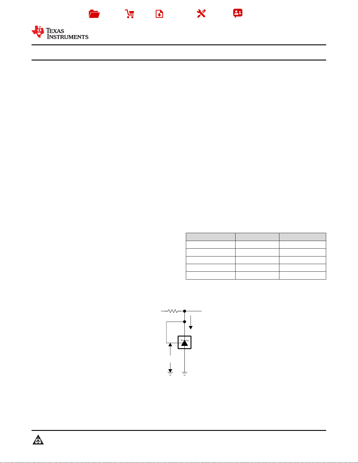
V
REF
Input
V
I
O
K
Product
Folder
Order
Now
Technical
Documents
Tools &
Software
Support &
Community
TLVH431,TLVH431A,TLVH431B
TLVH432,TLVH432A,TLVH432B
SLVS555L –NOVEMBER 2004–REVISED APRIL 2020
TLVH431, TLVH432 Low-Voltage Adjustable Precision Shunt Regulators
1 Features
1
• Low-voltage operation: down to 1.24 V
• Reference voltage tolerances at 25°C
– 0.5% for B grade
– 1% for A grade
– 1.5% for standard grade
• Adjustable output voltage, VO= V
REF
to 18 V
• Wide operating cathode current range:
100 μA to 70 mA
• 0.25-Ω typical output impedance
• –40°C to +125°C specifications
• TLVH432 provides alternative pinouts for
SOT-23-3 and SOT-89 packages
• Ultra-small SC-70 package offers 40%
smaller footprint than SOT-23-3
2 Applications
• Adjustable voltage reference for data Converters
• Secondary side regulation in flyback SMPSs
• Zener replacement with low leakage current
• Voltage monitoring for power rails
• Comparator with integrated reference
3 Description
The TLVH431 and TLVH432 devices are low-voltage
3-terminal adjustable voltage references, with
specified thermal stability over applicable industrial
and commercial temperature ranges. Output voltage
can be set to any value between V
18 V with two external resistors (see Figure 19).
These devices operate from a lower voltage (1.24 V)
than the widely used TL431 and TL1431 shuntregulator references.
When used with an optocoupler, the TLVH431 and
TLVH432 devices are ideal voltage references in
isolated feedback circuits for 3-V to 3.3-V switchingmode power supplies. They have a typical output
impedance of 0.25 Ω. Active output circuitry provides
a very sharp turn-on characteristic, making the
TLVH431 and TLVH432 devices excellent
replacements for low-voltage Zener diodes in many
applications, including on-board regulation and
adjustable power supplies.
The TLVH432 device is identical to the TLVH431
device, but is offered with different pinouts for the
3-pin SOT-23 and SOT-89 packages.
Device Information
PART NUMBER PACKAGE BODY SIZE (NOM)
TLVH43xxDBZ SOT-23 (5) 2.90 mm × 1.60 mm
TLVH43xxDBZ SOT-23 (3) 2.92 mm × 1.30 mm
TLVH43xxDCK SC70 (6) 2.00 mm × 1.25 mm
TLVH43xxLP TO-92 (3) 4.30 mm × 4.30 mm
TLVH43xxPK SOT-89 (3) 4.50 mm × 2.50 mm
(1) For all available packages, see the orderable addendum at
the end of the data sheet.
(1.24 V) and
REF
(1)
Simplified Schematic
1
An IMPORTANT NOTICE at the end of this data sheet addresses availability, warranty, changes, use in safety-critical applications,
intellectual property matters and other important disclaimers. PRODUCTION DATA.

TLVH431,TLVH431A,TLVH431B
TLVH432,TLVH432A,TLVH432B
SLVS555L –NOVEMBER 2004–REVISED APRIL 2020
www.ti.com
Table of Contents
1 Features.................................................................. 1
2 Applications ........................................................... 1
3 Description ............................................................. 1
4 Revision History..................................................... 2
5 Pin Configuration and Functions......................... 3
6 Specifications......................................................... 4
6.1 Absolute Maximum Ratings ...................................... 4
6.2 ESD Ratings.............................................................. 4
6.3 Recommended Operating Conditions....................... 4
6.4 Thermal Information.................................................. 4
6.5 TLVH43x Electrical Characteristics........................... 5
6.6 TLVH43xA Electrical Characteristics ........................ 6
6.7 TLVH43xB Electrical Characteristics ........................ 7
6.8 Typical Characteristics.............................................. 8
7 Parameter Measurement Information ................ 15
8 Detailed Description............................................ 16
8.1 Overview ................................................................. 16
8.2 Functional Block Diagram....................................... 16
8.3 Feature Description................................................. 17
8.4 Device Functional Modes........................................ 18
9 Applications and Implementation ...................... 19
9.1 Application Information............................................ 19
9.2 Typical Applications ................................................ 20
10 Power Supply Recommendations ..................... 24
11 Layout................................................................... 24
11.1 Layout Guidelines ................................................. 24
11.2 Layout Example .................................................... 24
12 Device and Documentation Support................. 25
12.1 Documentation Support ........................................ 25
12.2 Receiving Notification of Documentation Updates 25
12.3 Community Resources.......................................... 25
12.4 Related Links ........................................................ 25
12.5 Trademarks........................................................... 25
12.6 Electrostatic Discharge Caution............................ 25
12.7 Glossary................................................................ 25
13 Mechanical, Packaging, and Orderable
Information........................................................... 25
4 Revision History
NOTE: Page numbers for previous revisions may differ from page numbers in the current version.
Changes from Revision K (September 2016) to Revision L Page
• Added links to applications on TI.com ................................................................................................................................... 1
• Changed Thermal Information................................................................................................................................................ 4
• Changed load capacitance value to better reflect the device behavior................................................................................ 22
Changes from Revision J (January 2015) to Revision K Page
• Changed data sheet title......................................................................................................................................................... 1
• Updated pinout images and Pin Functions table.................................................................................................................... 3
• Deleted D package from Pin Functions table......................................................................................................................... 3
• Added Receiving Notification of Documentation Updates section and Community Resources section.............................. 25
Changes from Revision I (September 2009) to Revision J Page
• Added Applications, Device Information table, Pin Functions table, ESD Ratings table, Thermal Information table,
Typical Characteristics, Feature Description section, Device Functional Modes, Application and Implementation
section, Power Supply Recommendations section, Layout section, Device and Documentation Support section, and
Mechanical, Packaging, and Orderable Information section.................................................................................................. 1
• Deleted Ordering Information table. ....................................................................................................................................... 1
2
Submit Documentation Feedback Copyright © 2004–2020, Texas Instruments Incorporated
Product Folder Links: TLVH431 TLVH431A TLVH431B TLVH432 TLVH432A TLVH432B
3 REF
2 ANODE
1 CATHODE
Not to scale
Not to scale
1 CATHODE
2 ANODE
3 REF
3 CATHODE
2 ANODE
1 REF
Not to scale
1CATHODE 6 ANODE
2NC 5 NC
3REF 4 NC
Not to scale
1CATHODE
2REF
3 ANODE
Not to scale
1NC
2*
3CATHODE 4 REF
5 ANODE
Not to scale
1REF
2CATHODE
3 ANODE
Not to scale
www.ti.com
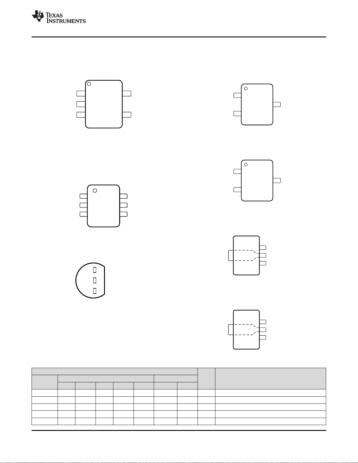
5 Pin Configuration and Functions
TLVH431,TLVH431A,TLVH431B
TLVH432,TLVH432A,TLVH432B
SLVS555L –NOVEMBER 2004–REVISED APRIL 2020
TLVH431 DBV Package
5-Pin SOT-23
Top View
NC – No internal connection
* Pin 2 is attached to Substrate and must
be connected to ANODE or left open.
TLVH431 DCK Package
6-Pin SC70
Top View
TLVH431 DBZ Package
3-Pin SOT-23
Top View
TLVH432 DBZ Package
3-Pin SOT-23
Top View
TLVH431 PK Package
3-Pin SOT-89
Top View
NAME
CATHODE 2 3 1 1 3 1 1 I/O Shunt Current/Voltage input
REF 1 4 3 3 1 2 3 I Threshold relative to common anode
ANODE 3 5 2 6 2 3 2 O Common pin, normally connected to ground
NC — 1 — 2, 4, 5 — — — I No Internal Connection
* — 2 — — — — — I Substrate Connection
TLVH431 LP Package
3-Pin TO-92
Top View
Pin Functions
PIN
TLVH431 TLVH432
DBZ DBV LP DCK PK DBZ PK
Product Folder Links: TLVH431 TLVH431A TLVH431B TLVH432 TLVH432A TLVH432B
TLVH432 PK Package
3-Pin SOT-89
Top View
TYPE DESCRIPTION
Submit Documentation FeedbackCopyright © 2004–2020, Texas Instruments Incorporated
3
TLVH431,TLVH431A,TLVH431B
TLVH432,TLVH432A,TLVH432B
SLVS555L –NOVEMBER 2004–REVISED APRIL 2020
www.ti.com
6 Specifications
6.1 Absolute Maximum Ratings
over operating free-air temperature range (unless otherwise noted)
V
KA
I
K
I
ref
T
J
T
stg
Cathode voltage
Cathode current –25 80 mA
Reference current –0.05 3 mA
Operating virtual junction temperature 150 °C
Storage temperature –65 150 °C
(1) Stresses beyond those listed under Absolute Maximum Ratings may cause permanent damage to the device. These are stress ratings
only, which do not imply functional operation of the device at these or any other conditions beyond those indicated under Recommended
Operating Conditions. Exposure to absolute-maximum-rated conditions for extended periods may affect device reliability.
(2) Voltage values are with respect to the anode terminal, unless otherwise noted.
(2)
6.2 ESD Ratings
V
(ESD)
Electrostatic
discharge
(1) JEDEC document JEP155 states that 500-V HBM allows safe manufacturing with a standard ESD control process.
(2) JEDEC document JEP157 states that 250-V CDM allows safe manufacturing with a standard ESD control process.
Human body model (HBM), per ANSI/ESDA/JEDEC JS-001
Charged device model (CDM), per JEDEC specification JESD22-C101
(1)
MIN MAX UNIT
20 V
VALUE UNIT
(1)
(2)
±2000
±1000
V
6.3 Recommended Operating Conditions
(1)
See
MIN MAX UNIT
V
I
Cathode voltage V
KA
Cathode current (continuous) 0.1 70 mA
K
REF
18 V
TLVH43x_C 0 70
T
Operating free-air temperature
A
°CTLVH43x_I –40 85
TLVH43x_Q –40 125
(1) Maximum power dissipation is a function of TJ(max), θJA, and TA. The maximum allowable power dissipation at any allowable ambient
temperature is PD= (TJ(max) – TA) / θJA. Operating at the absolute maximum TJof 150°C can affect reliability.
6.4 Thermal Information
TLVH43xx
THERMAL METRIC
(1)
DCK
(SC70)PK(SOT-89)
6 PINS 3 PINS 5 PINS 3 PINS 3 PINS
R
θJA
R
θJC(top)
Junction-to-ambient thermal resistance 259 52 206 206 140 °C/W
Junction-to-case (top) thermal resistance 87 9 131 76 55 °C/W
(1) For more information about traditional and new thermal metrics, see the Semiconductor and IC Package Thermal Metrics application
report.
DBV
(SOT-23)
DBZ
(SOT-23)LP(TO-92)
UNIT
4
Submit Documentation Feedback Copyright © 2004–2020, Texas Instruments Incorporated
Product Folder Links: TLVH431 TLVH431A TLVH431B TLVH432 TLVH432A TLVH432B

ka ka
V
z z
I
R1
1
R2
D
D
+¢ = » ´
æ ö
ç ÷
è ø
KA
K
ka
V
z
IDD
=
( )
REF( dev)
6
REF A
REF
A
V
10
V T 25 C
ppm
V
C T
´
= °
a =
° D
æ ö
ç ÷
æ ö
è ø
ç ÷
è ø
DV
REF
DV
KA
TLVH431,TLVH431A,TLVH431B
TLVH432,TLVH432A,TLVH432B
www.ti.com
SLVS555L –NOVEMBER 2004–REVISED APRIL 2020
6.5 TLVH43x Electrical Characteristics
at 25°C free-air temperature (unless otherwise noted)
TLVH431
PARAMETER TEST CONDITIONS
TA= 25°C 1.222 1.24 1.258
V
REF
Reference voltage
VKA= V
IK= 10 mA
REF
,
TA= full range,
See Figure 18
(1)
TLVH431C 1.21 1.27
TLVH431I 1.202 1.278
TLVH431Q 1.194 1.286
TLVH431C 4 12
V
REF(dev)
deviation over full
REF
temperature range
(2)
VKA= V
, IK= 10 mA, See Figure 18
REF
(1)
V
TLVH431Q 11 31
Ratio of V
cathode voltage change
I
ref
Reference terminal current IK= 10 mA, R1 = 10 kΩ, R2 = open, See Figure 19 0.1 0.5 μA
REF
change to
IK= 10 mA, VK= V
to 18 V, See Figure 19 –1.5 –2.7 mV/V
REF
TLVH431C 0.05 0.3
I
ref(dev)
deviation over full
ref
temperature range
(2)
IK= 10 mA, R1 = 10 kΩ, R2 = open,
See Figure 19
(1)
I
TLVH431Q 0.15 0.5
I
K(min)
I
K(off)
|zKA| Dynamic impedance
Minimum cathode current
for regulation
Off-state cathode current V
(3)
VKA= V
REF
VKA= V
See Figure 18
, See Figure 18 60 100 μA
REF
= 0, VKA= 18 V, See Figure 20 0.02 0.1 μA
, f ≤ 1 kHz, IK= 0.1 mA to 70 mA,
REF
(1) Full temperature ranges are –40°C to +125°C for TLVH431Q, –40°C to +85°C for TLVH431I, and 0°C to 70°C for TLVH431C.
(2) The deviation parameters V
the rated temperature range. The average full-range temperature coefficient of the reference input voltage, αV
REF(dev)
and I
are defined as the differences between the maximum and minimum values obtained over
ref(dev)
TLVH432
MIN TYP MAX
0.25 0.4 Ω
, is defined as:
REF
UNIT
V
mVTLVH431I 6 20
μATLVH431I 0.1 0.4
where ΔTAis the rated operating free-air temperature range of the device.
αV
can be positive or negative, depending on whether minimum V
REF
temperature.
or maximum V
REF
, respectively, occurs at the lower
REF
(3) The dynamic impedance is defined as:
When the device is operating with two external resistors (see Figure 19), the total dynamic impedance of the circuit is defined as:
Submit Documentation FeedbackCopyright © 2004–2020, Texas Instruments Incorporated
Product Folder Links: TLVH431 TLVH431A TLVH431B TLVH432 TLVH432A TLVH432B
5
ka ka
V
z z
I
R1
1
R2
D
D
+¢ = » ´
æ ö
ç ÷
è ø
KA
K
ka
V
z
IDD
=
( )
REF( dev)
6
REF A
REF
A
V
10
V T 25 C
ppm
V
C T
´
= °
a =
° D
æ ö
ç ÷
æ ö
è ø
ç ÷
è ø
DV
REF
DV
KA
TLVH431,TLVH431A,TLVH431B
TLVH432,TLVH432A,TLVH432B
SLVS555L –NOVEMBER 2004–REVISED APRIL 2020
6.6 TLVH43xA Electrical Characteristics
at 25°C free-air temperature (unless otherwise noted)
TLVH431A
PARAMETER TEST CONDITIONS
TA= 25°C 1.228 1.24 1.252
V
REF
Reference voltage
VKA= V
IK= 10 mA
REF
,
TA= full range,
See Figure 18
(1)
TLVH431AC 1.221 1.259
TLVH431AI 1.215 1.265
TLVH431AQ 1.209 1.271
TLVH431AC 4 12
V
REF(dev)
deviation over full
REF
temperature range
(2)
VKA= V
, IK= 10 mA, See Figure 18
REF
(1)
V
TLVH431AQ 11 31
Ratio of V
cathode voltage change
I
ref
Reference terminal current IK= 10 mA, R1 = 10 kΩ, R2 = open, See Figure 19 0.1 0.5 μA
REF
change to
VK= V
to 18 V, IK= 10 mA, See Figure 19 –1.5 –2.7 mV/V
REF
TLVH431AC 0.05 0.3
I
ref(dev)
deviation over full
ref
temperature range
(2)
IK= 10 mA, R1 = 10 kΩ, R2 = open,
See Figure 19
(1)
I
TLVH431AQ 0.15 0.5
I
K(min)
I
K(off)
|zKA| Dynamic impedance
Minimum cathode current
for regulation
Off-state cathode current V
(3)
VKA= V
REF
VKA= V
See Figure 18
, See Figure 18 60 100 μA
REF
= 0, VKA= 18 V, See Figure 20 0.02 0.1 μA
, f ≤ 1 kHz, IK= 0.1 mA to 70 mA,
REF
(1) Full temperature ranges are –40°C to +125°C for TLVH431Q, –40°C to +85°C for TLVH431I, and 0°C to 70°C for TLVH431C.
(2) The deviation parameters V
the rated temperature range. The average full-range temperature coefficient of the reference input voltage, αV
REF(dev)
and I
are defined as the differences between the maximum and minimum values obtained over
ref(dev)
TLVH432A
MIN TYP MAX
0.25 0.4 Ω
, is defined as:
REF
www.ti.com
UNIT
V
mVTLVH431AI 6 20
μATLVH431AI 0.1 0.4
where ΔTAis the rated operating free-air temperature range of the device.
αV
can be positive or negative, depending on whether minimum V
REF
temperature.
or maximum V
REF
, respectively, occurs at the lower
REF
(3) The dynamic impedance is defined as:
When the device is operating with two external resistors (see Figure 19), the total dynamic impedance of the circuit is defined as:
6
Submit Documentation Feedback Copyright © 2004–2020, Texas Instruments Incorporated
Product Folder Links: TLVH431 TLVH431A TLVH431B TLVH432 TLVH432A TLVH432B
ka ka
V
z z
I
R1
1
R2
D
D
+¢ = » ´
æ ö
ç ÷
è ø
KA
K
ka
V
z
IDD
=
( )
REF( dev)
6
REF A
REF
A
V
10
V T 25 C
ppm
V
C T
´
= °
a =
° D
æ ö
ç ÷
æ ö
è ø
ç ÷
è ø
DV
REF
DV
KA
TLVH431,TLVH431A,TLVH431B
TLVH432,TLVH432A,TLVH432B
www.ti.com
SLVS555L –NOVEMBER 2004–REVISED APRIL 2020
6.7 TLVH43xB Electrical Characteristics
at 25°C free-air temperature (unless otherwise noted)
TLVH431B
PARAMETER TEST CONDITIONS
TA= 25°C 1.234 1.24 1.246
V
REF
Reference voltage
VKA= V
IK= 10 mA
REF
,
TA= full range,
See Figure 18
(1)
TLVH431BC 1.227 1.253
TLVH431BI 1.224 1.259
TLVH431BQ 1.221 1.265
TLVH431BC 4 12
V
REF(dev)
deviation over full
REF
temperature range
(2)
VKA= V
, IK= 10 mA, See Figure 18
REF
(1)
V
TLVH431BQ 11 31
Ratio of V
cathode voltage change
I
ref
Reference terminal current IK= 10 mA, R1 = 10 kΩ, R2 = open, See Figure 19 0.1 0.5 μA
REF
change to
IK= 10 mA, VK= V
to 18 V, See Figure 19 –1.5 –2.7 mV/V
REF
TLVH431BC 0.05 0.3
I
ref(dev)
deviation over full
ref
temperature range
(2)
IK= 10 mA, R1 = 10 kΩ, R2 = open,
See Figure 19
(1)
I
TLVH431BQ 0.15 0.5
I
K(min)
I
K(off)
|zKA| Dynamic impedance
Minimum cathode current
for regulation
Off-state cathode current V
(3)
VKA= V
REF
VKA= V
, See Figure 18 60 100 μA
REF
= 0, VKA= 18 V, See Figure 20 0.02 0.1 μA
, f ≤ 1 kHz, IK= 0.1 mA to 70 mA, See Figure 18 0.25 0.4 Ω
REF
(1) Full temperature ranges are –40°C to +125°C for TLVH431Q, –40°C to +85°C for TLVH431I, and 0°C to 70°C for TLVH431C.
(2) The deviation parameters V
the rated temperature range. The average full-range temperature coefficient of the reference input voltage, αV
REF(dev)
and I
are defined as the differences between the maximum and minimum values obtained over
ref(dev)
TLVH432B
MIN TYP MAX
, is defined as:
REF
UNIT
V
mVTLVH431BI 6 20
μATLVH431BI 0.1 0.4
where ΔTAis the rated operating free-air temperature range of the device.
αV
can be positive or negative, depending on whether minimum V
REF
temperature.
or maximum V
REF
, respectively, occurs at the lower
REF
(3) The dynamic impedance is defined as:
When the device is operating with two external resistors (see Figure 19), the total dynamic impedance of the circuit is defined as:
Submit Documentation FeedbackCopyright © 2004–2020, Texas Instruments Incorporated
Product Folder Links: TLVH431 TLVH431A TLVH431B TLVH432 TLVH432A TLVH432B
7
0
500
1000
1500
2000
2500
3000
3500
4000
−50 −25 0 25 50 75 100 125 150
VKA= 5 V
V
REF
= 0
TJ− Junction Temperature − °C
− Off-State Cathode Current − nA
I
K(off)
Temperature (qC)
Ik(min)
-40 -20 0 20 40 60 80 100 120 140
55
60
65
70
75
80
85
90
95
100
105
110
115
120
− Cathode Current − mA
70
10
5
0
−5
−10
−15
−1 − 0.5 0 0.5 1 1.5
I
K
VKA= V
REF
TA= 25°C
VKA− Cathode Voltage − V
~
~
~
~
− Cathode Current −
250
200
150
100
50
0
−200
−250
−1 −0.5 0 0.5 1 1.5
I
K
Aµ
V
− Cathode Voltage − V
−50
−100
−150
VKA= V
REF
TA= 25°C
50
70
90
110
130
150
170
190
210
230
250
−50 −25 0 25 50 75 100 125 150
IK= 10 mA
R1 = 10 kΩ
R2 = Open
− Reference Input Current − nA
I
ref
TJ− Junction Temperature − °C
1.246
1.242
1.240
1.238
− Reference V
oltage − V
1.250
1.252
1.254
1.248
1.244
−50 − 25 0 25 50 75 100 125 150
IK= 10 mA
V
ref
TJ− Junction Temperature − °C
TLVH431,TLVH431A,TLVH431B
TLVH432,TLVH432A,TLVH432B
SLVS555L –NOVEMBER 2004–REVISED APRIL 2020
www.ti.com
6.8 Typical Characteristics
Operation of the device at these or any other conditions beyond those indicated in the Recommended Operating Conditions
table are not implied.
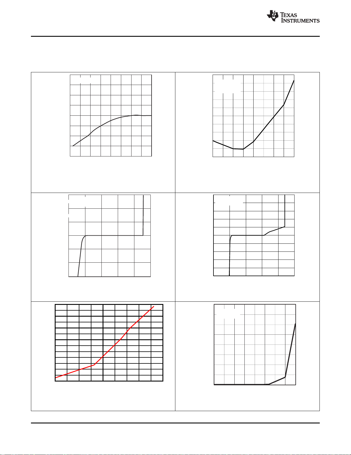
Figure 1. Reference Voltage
vs Junction Temperature
Figure 2. Reference Input Current
vs Junction Temperature
Figure 3. Cathode Current
vs Cathode Voltage
Figure 5. Minimum Cathode Current vs. Temperature
8
Submit Documentation Feedback Copyright © 2004–2020, Texas Instruments Incorporated
Product Folder Links: TLVH431 TLVH431A TLVH431B TLVH432 TLVH432A TLVH432B
Figure 4. Cathode Current
vs Cathode Voltage
Figure 6. Off-State Cathode Current
vs Junction Temperature
200
150
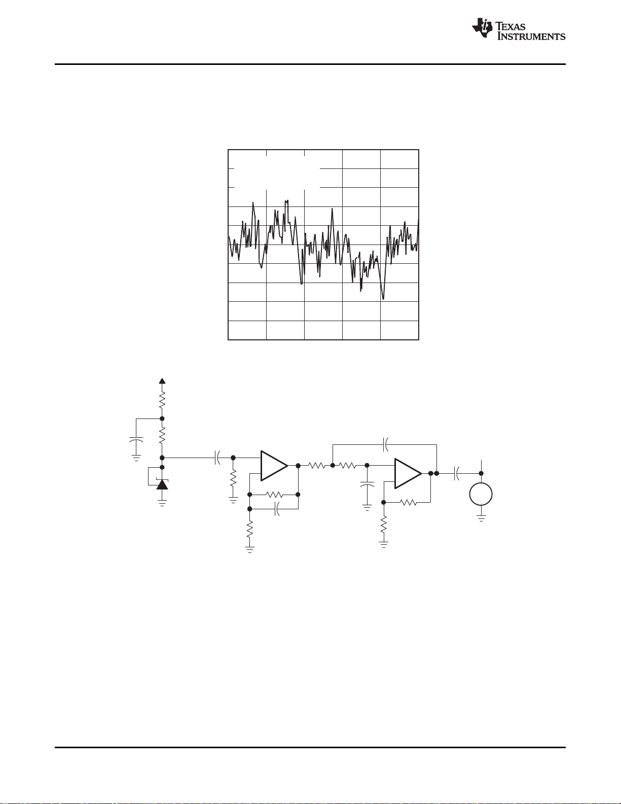
10 100 1 k
− Equivalent Input Noise V
oltage −
EQUIVALENT INPUT NOISE VOLTAGE
vs
FREQUENCY
350
10 k 100 k
300
250
V
n
(nV/
Hz)
VKA= V
REF
IK= 1 mA
TA= 25°C
_
+
820 W
+
2200 mF
750 W
1 kW
470 mF
3 V
TLVH431
TLVH432
TP
160 kW
160 W
TLE2027
TEST CIRCUIT FOR EQUIVALENT INPUT NOISE VOLTAGE
+
f – Frequency – (Hz)
− 0.025
− 0.075
− 0.1
− 0.125
Percentage Change in V
ref − %
0.025
0
− 0.05
0 10 20 30 40 50 60
IK= 1 mA
V
ref
Operating Life at 55°C − kh
(1)
% Change (3
δ
)
% Change (−3
δ
)
% Change (avg)
(1) Extrapolated from life-test data taken at 125°C; the activation energy
assumed is 0.7 eV.
−1.0
−0.9
−0.8
−0.7
−0.6
−0.5
−0.4
−0.3
−0.2
−0.1
0.0
−50 −25 0 25 50 75 100 125 150
IK= 10 mA
ΔV
KA
= V
REF
to 18 V
− Ratio of Delta Reference V
oltage
to Delta Cathode V
oltage − mV/V
V
ref/
Δ
V
KA
Δ
TJ− Junction Temperature − °C
−1
0
TLVH431,TLVH431A,TLVH431B
TLVH432,TLVH432A,TLVH432B
www.ti.com
SLVS555L –NOVEMBER 2004–REVISED APRIL 2020
Typical Characteristics (continued)
Operation of the device at these or any other conditions beyond those indicated in the Recommended Operating Conditions
table are not implied.
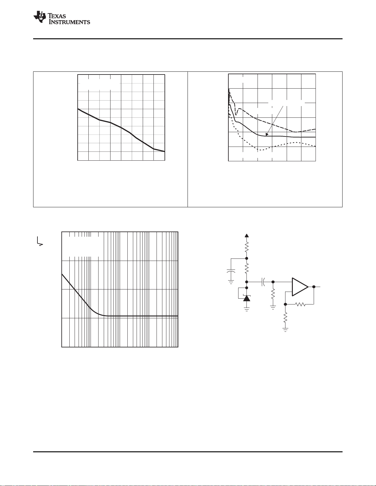
Figure 7. Ratio of Delta Reference Voltage to Delta Cathode
Voltage
vs Junction Temperature
Product Folder Links: TLVH431 TLVH431A TLVH431B TLVH432 TLVH432A TLVH432B
Figure 8. Percentage Change in V
Figure 9. Equivalent Input Noise Voltage
vs
Operating Life at 55°C
Submit Documentation FeedbackCopyright © 2004–2020, Texas Instruments Incorporated
REF
9
0 2 4 6
t − Time − (s)
EQUIVALENT INPUT NOISE VOLTAGE
OVER A 10-S PERIOD
8 10
10
8
6
4
2
0
−2
−4
−6
−8
−10
f = 0.1 Hz to 10 Hz
IK= 1 mA
TA= 25°C
− Equivalent Input Noise V
oltage −
V
n
V)
(m
_
+
1 mF
750 W
1 kW
470 mF
3 V
TLVH431
TLVH432
33 kW
TLE2027
TEST CIRCUIT FOR 0.1-Hz TO 10-Hz EQUIVALENT NOISE VOLTAGE
+
33 kW
10 kW
_
+
16 W
0.1 mF
160 kW
820 W
+
2200 mF
TP
2.2 mF
CRO
1 MW
TLE2027
0.47 mF
10 kW
+
TLVH431,TLVH431A,TLVH431B
TLVH432,TLVH432A,TLVH432B
SLVS555L –NOVEMBER 2004–REVISED APRIL 2020
www.ti.com
Typical Characteristics (continued)
Operation of the device at these or any other conditions beyond those indicated in the Recommended Operating Conditions
table are not implied.
Figure 10. Equivalent Input Noise Voltage
10
Submit Documentation Feedback Copyright © 2004–2020, Texas Instruments Incorporated
Product Folder Links: TLVH431 TLVH431A TLVH431B TLVH432 TLVH432A TLVH432B
Input and Output Voltage − V
Output
R = 18 kΩ
T
A
= 25°C
18 kΩ
50 Ω
GND
Output
Pulse
Generator
f = 100 kHz
TEST CIRCUIT FOR PULSE RESPONSE 1
0 1 2 3 4
PULSE RESPONSE 1
5 6 7 8
3.5
3
2.5
2
1.5
1
0.5
0
−0.5
t − Time − µs
Input
I
k
SMALL-SIGNAL VOLTAGE GAIN
/PHASE MARGIN
vs
FREQUENCY
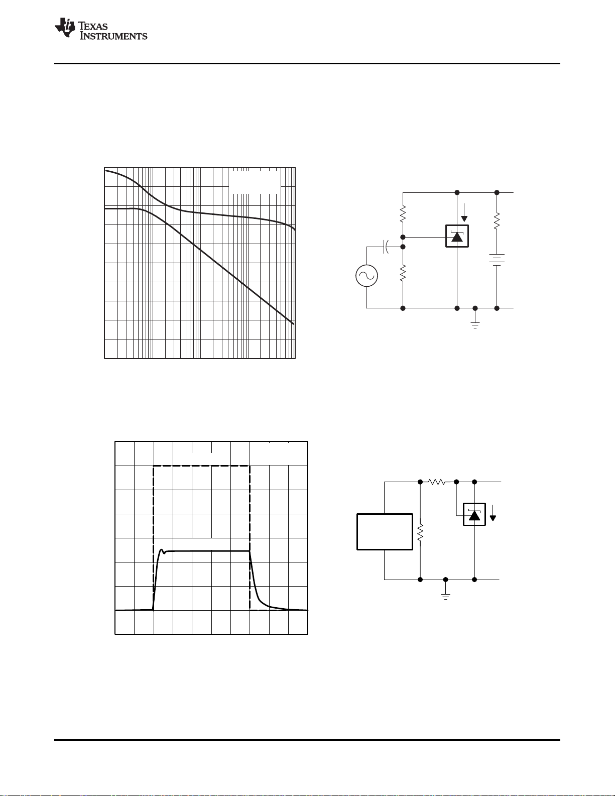
10 mF
GND
Output
180 W
I
K
6.8 kW
1 k 10 k 100 k 1 M100
− Small-Signal V
oltage Gain/Phase Margin − (dB)
f − Frequency − (Hz)
A
V
TEST CIRCUIT FOR VOLTAGE GAIN
AND PHASE MARGIN
80
70
60
50
40
30
20
10
0
−10
0°
36°
72°
108°
144°
180°
Phase Shift
4.3 kW
5 V
IK= 10 mA
TA= 25°C
−20
TLVH431,TLVH431A,TLVH431B
TLVH432,TLVH432A,TLVH432B
www.ti.com
SLVS555L –NOVEMBER 2004–REVISED APRIL 2020
Typical Characteristics (continued)
Operation of the device at these or any other conditions beyond those indicated in the Recommended Operating Conditions
table are not implied.
Figure 11. Voltage Gain and Phase Margin
Product Folder Links: TLVH431 TLVH431A TLVH431B TLVH432 TLVH432A TLVH432B
Figure 12. Pulse Response 1
Submit Documentation FeedbackCopyright © 2004–2020, Texas Instruments Incorporated
11
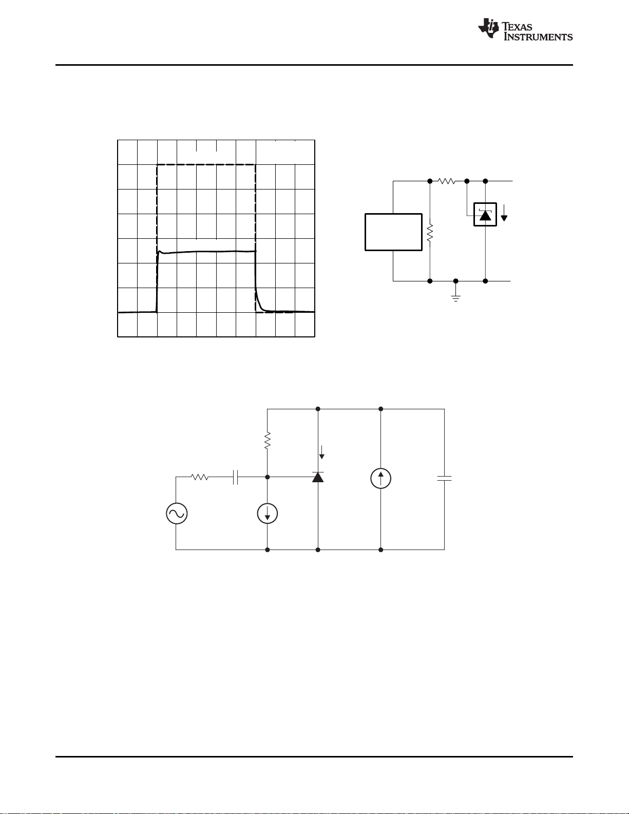
50 W
100 µF
30 kW
I
1
I
K
I
2
C
L
Input and Output Voltage − V
Output
R = 1.8 kΩ
T
A
= 25°C
1.8 kΩ
50 Ω
GND
Output
Pulse
Generator
f = 100 kHz
TEST CIRCUIT FOR PULSE RESPONSE 2
0 1 2 3 4
PULSE RESPONSE 2
5 6 7 8
3.5
3
2.5
2
1.5
1
0.5
0
−0.5
t − Time − µs
Input
I
K
TLVH431,TLVH431A,TLVH431B
TLVH432,TLVH432A,TLVH432B
SLVS555L –NOVEMBER 2004–REVISED APRIL 2020
www.ti.com
Typical Characteristics (continued)
Operation of the device at these or any other conditions beyond those indicated in the Recommended Operating Conditions
table are not implied.
Figure 13. Pulse Response 2
Figure 14. Phase Margin Test Circuit
12
Submit Documentation Feedback Copyright © 2004–2020, Texas Instruments Incorporated
Product Folder Links: TLVH431 TLVH431A TLVH431B TLVH432 TLVH432A TLVH432B
I
K
I
K
TLVH431,TLVH431A,TLVH431B
TLVH432,TLVH432A,TLVH432B
www.ti.com
SLVS555L –NOVEMBER 2004–REVISED APRIL 2020
Typical Characteristics (continued)
Operation of the device at these or any other conditions beyond those indicated in the Recommended Operating Conditions
table are not implied.
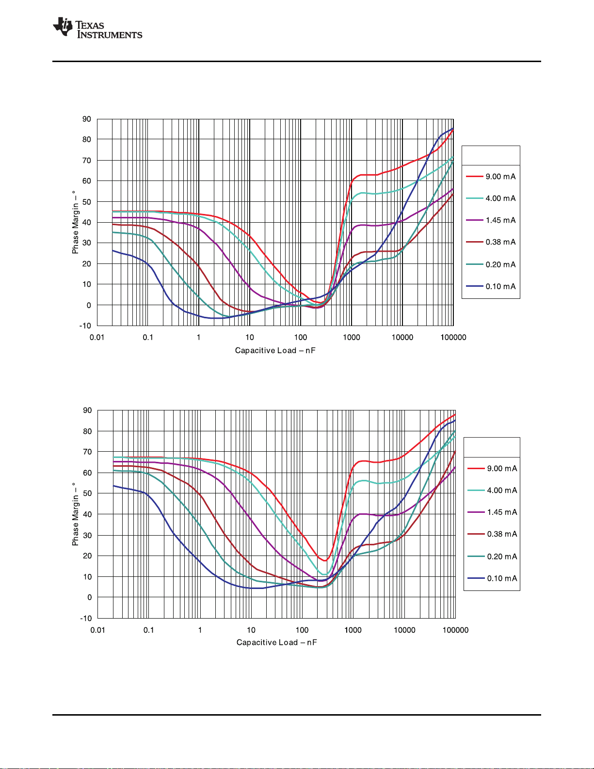
Figure 15. Phase Margin vs Capacitive Load
VKA= V
(1.25 V), TA= 25°C
REF
Figure 16. Phase Margin vs Capacitive Load
VKA= 2.50 V, TA= 25°C
Submit Documentation FeedbackCopyright © 2004–2020, Texas Instruments Incorporated
Product Folder Links: TLVH431 TLVH431A TLVH431B TLVH432 TLVH432A TLVH432B
13
I
K
TLVH431,TLVH431A,TLVH431B
TLVH432,TLVH432A,TLVH432B
SLVS555L –NOVEMBER 2004–REVISED APRIL 2020
www.ti.com
Typical Characteristics (continued)
Operation of the device at these or any other conditions beyond those indicated in the Recommended Operating Conditions
table are not implied.
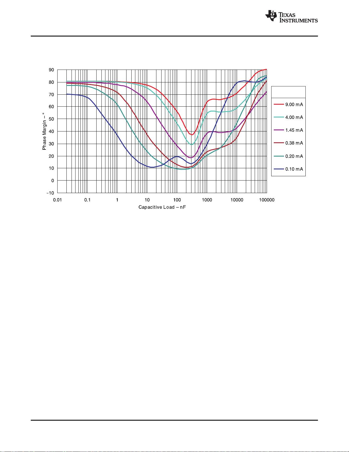
Figure 17. Phase Margin vs Capacitive Load
VKA= 5.00 V, TA= 25°C
14
Submit Documentation Feedback Copyright © 2004–2020, Texas Instruments Incorporated
Product Folder Links: TLVH431 TLVH431A TLVH431B TLVH432 TLVH432A TLVH432B
I
K(off)
V
O
Input
I
ref
I
K
V
O
Input
V
REF
R1
R2
V
REF
Input
V
O
I
K
www.ti.com
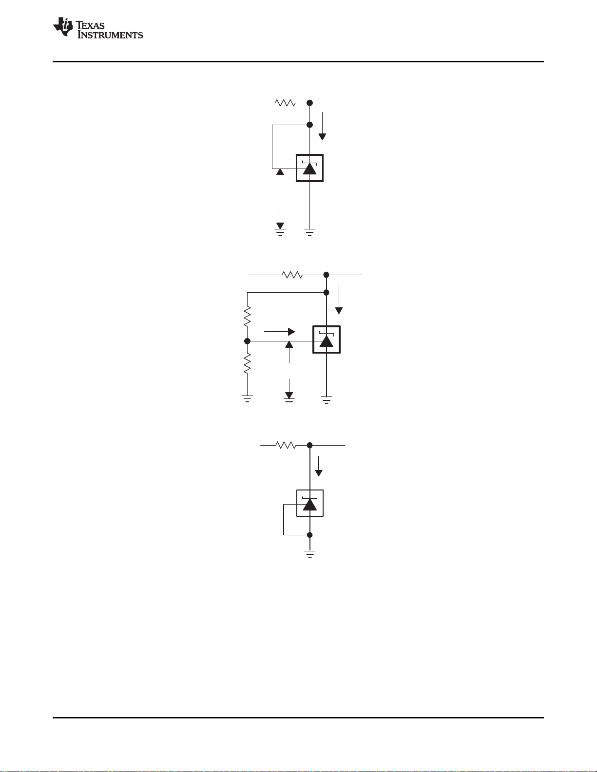
7 Parameter Measurement Information
TLVH431,TLVH431A,TLVH431B
TLVH432,TLVH432A,TLVH432B
SLVS555L –NOVEMBER 2004–REVISED APRIL 2020
Figure 18. Test Circuit for VKA= V
Figure 19. Test Circuit for VKA> V
, VO= VKA= V
REF
, VO= VKA= V
REF
× (1 + R1/R2) + I
REF
REF
ref
× R1
Figure 20. Test Circuit for I
Product Folder Links: TLVH431 TLVH431A TLVH431B TLVH432 TLVH432A TLVH432B
K(off)
Submit Documentation FeedbackCopyright © 2004–2020, Texas Instruments Incorporated
15
CATHODE
REF
ANODE
V
REF
= 1.24 V
−
+
TLVH431,TLVH431A,TLVH431B
TLVH432,TLVH432A,TLVH432B
SLVS555L –NOVEMBER 2004–REVISED APRIL 2020
www.ti.com
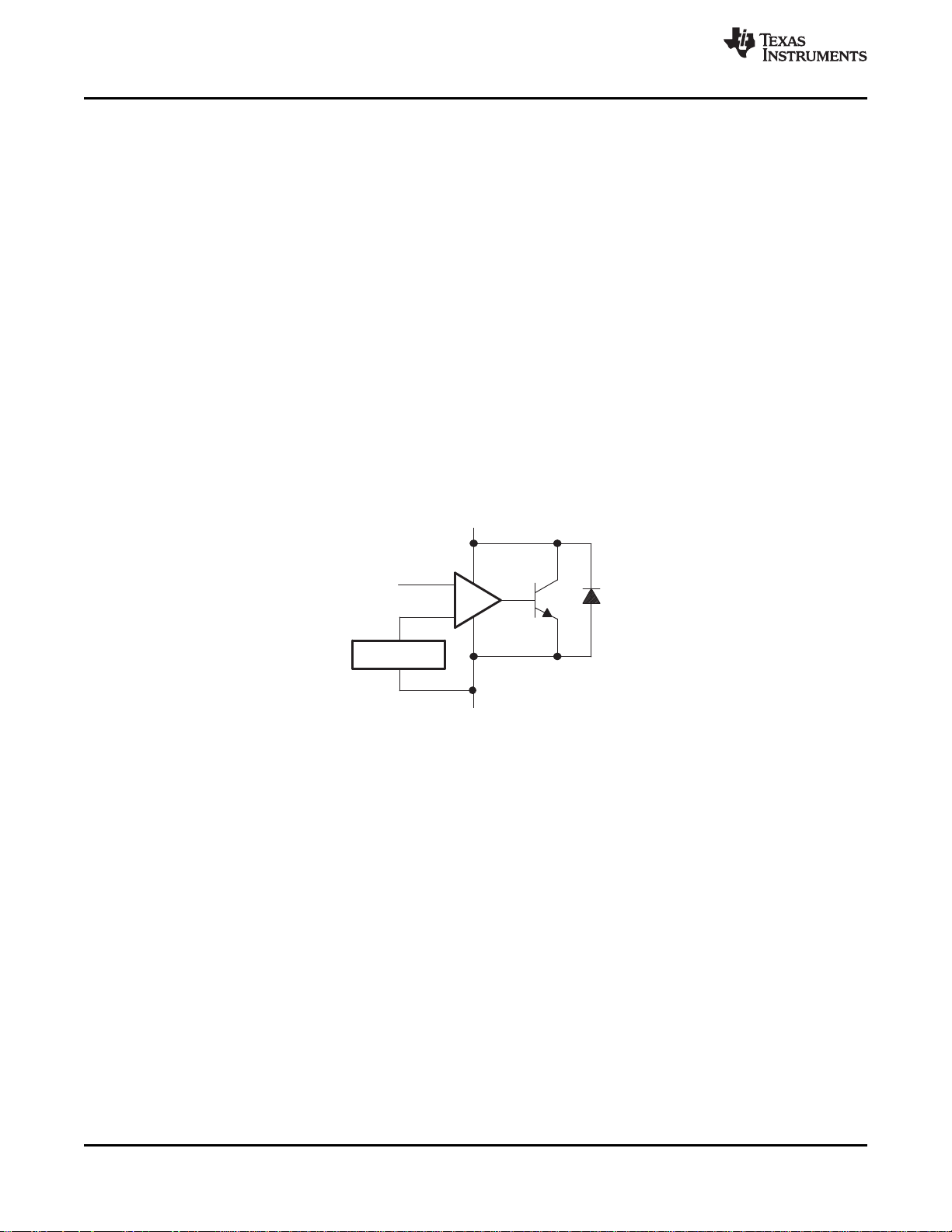
8 Detailed Description
8.1 Overview
TLVH431 is a low power counterpart to TL431, having lower reference voltage (1.24 V versus 2.5 V) for lower
voltage adjustability and lower minimum cathode current (I
used in conjunction with its key components to behave as a single voltage reference, error amplifier, voltage
clamp or comparator with integrated reference.
TLVH431 is also a higher voltage counterpart to TLV431, with cathode voltage adjustability from 1.24 V to 18 V,
making this part optimum for a wide range of end equipments in industrial, auto, telecom and computing. In order
for this device to behave as a shunt regulator or error amplifier, >100 µA (I
cathode pin. Under this condition, feedback can be applied from the Cathode and Ref pins to create a replica of
the internal reference voltage.
Various reference voltage options can be purchased with initial tolerances (at 25°C) of 0.5%, 1%, and 1.5%.
These reference options are denoted by B (0.5%), A (1.0%) and blank (1.5%) after the TLVH431.
The TLVH431xC devices are characterized for operation from 0°C to 70°C, the TLVH431xI devices are
characterized for operation from –40°C to +85°C, and the TLVH431xQ devices are characterized for operation
from –40°C to +125°C.
8.2 Functional Block Diagram
= 100 µA versus 1 mA). Like TL431, TLVH431 is
k(min)
(max)) must be supplied in to the
min
16
Figure 21. Equivalent Schematic
Submit Documentation Feedback Copyright © 2004–2020, Texas Instruments Incorporated
Product Folder Links: TLVH431 TLVH431A TLVH431B TLVH432 TLVH432A TLVH432B
REF
Cathode
Anode
www.ti.com
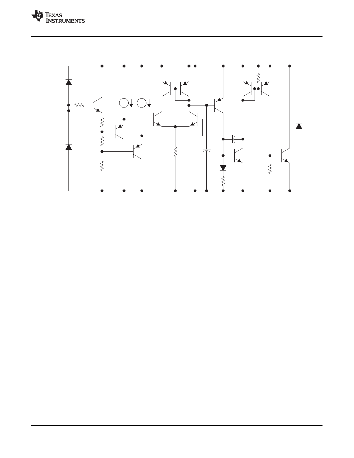
Functional Block Diagram (continued)
TLVH431,TLVH431A,TLVH431B
TLVH432,TLVH432A,TLVH432B
SLVS555L –NOVEMBER 2004–REVISED APRIL 2020
Figure 22. Detailed Schematic
8.3 Feature Description
TLVH431 consists of an internal reference and amplifier that outputs a sink current base on the difference
between the reference pin and the virtual internal pin. The sink current is produced by an internal Darlington pair.
When operated with enough voltage headroom (≥ 1.24 V) and cathode current (Ika), TLVH431 forces the
reference pin to 1.24 V. However, the reference pin can not be left floating, as it needs Iref ≥ 0.5 µA (see
Specifications). This is because the reference pin is driven into an NPN, which needs base current in order
operate properly.
When feedback is applied from the Cathode and Reference pins, TLVH431 behaves as a Zener diode, regulating
to a constant voltage dependent on current being supplied into the cathode. This is due to the internal amplifier
and reference entering the proper operating regions. The same amount of current needed in the above feedback
situation must be applied to this device in open loop, servo or error amplifying implementations in order for it to
be in the proper linear region giving TLVH431 enough gain.
Unlike many linear regulators, TLVH431 is internally compensated to be stable without an output capacitor
between the cathode and anode. However, if it is desired to use an output capacitor Figure 15, Figure 16, and
Figure 17 can be used as a guide to assist in choosing the correct capacitor to maintain stability.
Submit Documentation FeedbackCopyright © 2004–2020, Texas Instruments Incorporated
Product Folder Links: TLVH431 TLVH431A TLVH431B TLVH432 TLVH432A TLVH432B
17

TLVH431,TLVH431A,TLVH431B
TLVH432,TLVH432A,TLVH432B
SLVS555L –NOVEMBER 2004–REVISED APRIL 2020
www.ti.com
8.4 Device Functional Modes
8.4.1 Open Loop (Comparator)
When the cathode/output voltage or current of TLVH431 is not being fed back to the reference/input pin in any
form, this device is operating in open loop. With proper cathode current (Ika) applied to this device, TLVH431 has
the characteristics shown in Figure 4. With such high gain in this configuration, the TLVH431 device is typically
used as a comparator. With the reference integrated makes TLVH431 the preferred choice when users are trying
to monitor a certain level of a single signal.
8.4.2 Closed Loop
When the cathode/output voltage or current of TLVH431 is being fed back to the reference/input pin in any form,
this device is operating in closed loop. The majority of applications involving TLVH431 use it in this manner to
regulate a fixed voltage or current. The feedback enables this device to behave as an error amplifier, computing
a portion of the output voltage and adjusting it to maintain the desired regulation. This is done by relating the
output voltage back to the reference pin in a manner to make it equal to the internal reference voltage, which can
be accomplished through resistive or direct feedback.
18
Submit Documentation Feedback Copyright © 2004–2020, Texas Instruments Incorporated
Product Folder Links: TLVH431 TLVH431A TLVH431B TLVH432 TLVH432A TLVH432B

P
−
+
P
P
V
CC
V
FB
Current
Sense
Gate Drive
GND
Controller
P
P
P P
TLVH431
V
O
3.3 V
V
I
120 V
~
~
TLVH431,TLVH431A,TLVH431B
TLVH432,TLVH432A,TLVH432B
www.ti.com
SLVS555L –NOVEMBER 2004–REVISED APRIL 2020
9 Applications and Implementation
NOTE
Information in the following applications sections is not part of the TI component
specification, and TI does not warrant its accuracy or completeness. TI’s customers are
responsible for determining suitability of components for their purposes. Customers should
validate and test their design implementation to confirm system functionality.
9.1 Application Information
Figure 23 shows the TLVH431, TLVH431A, or TLVH431B used in a 3.3-V isolated flyback supply. Output voltage
VOcan be as low as reference voltage V
drop of the optocoupler LED (1.24 + 1.4 = 2.64 V), determine the minimum voltage that can be regulated in an
isolated supply configuration. Regulated voltage as low as 2.7 Vdc is possible in the topology shown in
Figure 23.
The TLVH431 family of devices are prevalent in these applications, being designers go to choice for secondary
side regulation. Due to this prevalence, this section explains operation and design in both states of TLVH431 that
this application will see, open loop (Comparator + V
Further information about system stability and using a TLVH431 device for compensation see Compensation
Design With TL431 for UCC28600, SLUA671.
(1.24 V ± 1%). The output of the regulator, plus the forward voltage
REF
) and closed loop (Shunt Regulator).
REF
Figure 23. Flyback With Isolation Using TLVH431 or TLVH432
as Voltage Reference and Error Amplifier
Product Folder Links: TLVH431 TLVH431A TLVH431B TLVH432 TLVH432A TLVH432B
Submit Documentation FeedbackCopyright © 2004–2020, Texas Instruments Incorporated
19

+
1.24 V
CATHODE
ANODE
REF
V
IN
Vout
Vsup
Rsup
R1
R2
V
L
R
IN
TLVH431,TLVH431A,TLVH431B
TLVH432,TLVH432A,TLVH432B
SLVS555L –NOVEMBER 2004–REVISED APRIL 2020
9.2 Typical Applications
9.2.1 Comparator With Integrated Reference (Open Loop)
Figure 24. Comparator Application Schematic
www.ti.com
9.2.1.1 Design Requirements
For this design example, use the parameters listed in Table 1 as the input parameters.
Table 1. Design Parameters
DESIGN PARAMETER EXAMPLE VALUE
Input Voltage Range 0 V to 5 V
Input Resistance 10 kΩ
Supply Voltage 9 V
Cathode Current (Ik) 500 µA
Output Voltage Level ~1 V - V
Logic Input Thresholds VIH/V
IL
sup
V
L
9.2.1.2 Detailed Design Procedure
When using TLVH431 as a comparator with reference, determine the following:
• Input voltage range
• Reference voltage accuracy
• Output logic input high and low level thresholds
• Current source resistance
9.2.1.2.1 Basic Operation
In the configuration shown in Figure 24, TLVH431 behaves as a comparator, comparing the V
pin voltage to
ref
the internal virtual reference voltage. When provided a proper cathode current (Ik), TLVH431 will have enough
open loop gain to provide a quick response. With the TLVH431's max Operating Current (I
up to 150 uA over temperature, operation below that could result in low gain, leading to a slow response.
) being 100 uA and
min
20
Submit Documentation Feedback Copyright © 2004–2020, Texas Instruments Incorporated
Product Folder Links: TLVH431 TLVH431A TLVH431B TLVH432 TLVH432A TLVH432B

Time (ms)
Voltage (V)
-0.4 -0.2 0 0.2 0.4 0.6 0.8
0
1
2
3
4
5
6
7
8
9
10
11
12
13
14
D001
Vin~1.24V (+/-5%)
Vo(Vin=1.18V)
Vo(Vin=1.24V)
Vo(Vin=1.30V)
Time (ms)
Voltage (V)
-0.4 -0.2 0 0.2 0.4 0.6 0.8
-2
-1
0
1
2
3
4
5
6
7
8
9
10
D001
Vo(Vin=5.0V)
Vin=5.0V
TLVH431,TLVH431A,TLVH431B
TLVH432,TLVH432A,TLVH432B
www.ti.com
9.2.1.2.2 Overdrive
SLVS555L –NOVEMBER 2004–REVISED APRIL 2020
Slow or inaccurate responses can also occur when the reference pin is not provided enough overdrive voltage.
This is the amount of voltage that is higher than the internal virtual reference. The internal virtual reference
voltage will be within the range of 1.24 V ±(0.5%, 1.0% or 1.5%) depending on which version is being used.
The more overdrive voltage provided, the faster the TLVH431 will respond. See figures Figure 25 and Figure 26,
for the output responses to various input voltages.
For applications where TLVH431 is being used as a comparator, it is best to set the trip point to greater than the
positive expected error (that is, +1.0% for the A version). For fast response, setting the trip point to > 10% of the
internal V
should suffice.
ref
For minimal voltage drop or difference from Vin to the ref pin, it is recommended to use an input resistor <10 kΩ
to provide I
9.2.1.2.3 Output Voltage and Logic Input Level
ref
.
In order for TLVH431 to properly be used as a comparator, the logic output must be readable by the receiving
logic device. This is accomplished by knowing the input high and low level threshold voltage levels, typically
denoted by VIHand VIL.
As shown in Figure 25 and Figure 26, TLVH431's output low level voltage in open-loop/comparator mode is
approximately 1 V, which is sufficient for some 3.3 V supplied logic. However, would not work for 2.5 V and 1.8 V
supplied logic. To accommodate this a resistive divider can be tied to the output to attenuate the output voltage
to a voltage legible to the receiving low voltage logic device.
TLVH431's output high voltage is approximately V
due to TLVH431 being open-collector. If V
SUP
SUP
is much
higher than the receiving logic's maximum input voltage tolerance, the output must be attenuated to
accommodate the outgoing logic's reliability.
When using a resistive divider on the output, be sure to make the sum of the resistive divider (R1 and R2 in
Figure 24) is much greater than R
in order to not interfere with TLVH431's ability to pull close to V
SUP
SUP
when
turning off.
9.2.1.2.3.1 Input Resistance
TLVH431 requires an input resistance in this application in order to source the reference current (I
from this device to be in the proper operating regions while turning on. The actual voltage seen at the ref pin will
be V
REF
= VIN– I
× RIN. Because I
REF
enough that will mitigate the error that I
9.2.1.3 Application Curves
Figure 25. Output Response With Small Overdrive
Product Folder Links: TLVH431 TLVH431A TLVH431B TLVH432 TLVH432A TLVH432B
Voltages
REF
can be as high as 0.5 µA, TI recommends to use a resistance small
REF
creates from VIN.
REF
Figure 26. Output Response With Large Overdrive Voltage
Submit Documentation FeedbackCopyright © 2004–2020, Texas Instruments Incorporated
) needed
21

REF
CATHODE
ANODE
V
SUP
R1
0.1%
R2
0.1%
TLVH431
C
L
R
SUP
V
REF
Copyright © 2016, Texas Instruments Incorporated
O REF
R 1
V ( 1 ) V
R 2
TLVH431,TLVH431A,TLVH431B
TLVH432,TLVH432A,TLVH432B
SLVS555L –NOVEMBER 2004–REVISED APRIL 2020
9.2.2 Shunt Regulator/Reference
Figure 27. Shunt Regulator Schematic
9.2.2.1 Design Requirements
For this design example, use the parameters listed in Table 2 as the input parameters.
Table 2. Design Parameters
DESIGN PARAMETER EXAMPLE VALUE
Reference Initial Accuracy 1.0%
Supply Voltage 6 V
Cathode Current (Ik) 500 µA
Output Voltage Level 1.24 V - 18 V
Load Capacitance 4.7 µF
Feedback Resistor Values and
Accuracy (R1 and R2)
10 kΩ
www.ti.com
9.2.2.2 Detailed Design Procedure
When using TLVH431 as a Shunt Regulator, determine the following:
• Input voltage range
• Temperature range
• Total accuracy
• Cathode current
• Reference initial accuracy
• Output capacitance
9.2.2.2.1 Programming Output/Cathode Voltage
To program the cathode voltage to a regulated voltage a resistive bridge must be shunted between the cathode
and anode pins with the mid point tied to the reference pin. This can be seen in Figure 27, with R1 and R2 being
the resistive bridge. The cathode/output voltage in the shunt regulator configuration can be approximated by the
equation shown in Figure 27. The cathode voltage can be more accurately determined by taking in to account
the cathode current:
VO=(1+R1/R2) × V
REF-IREF
× R1
In order for this equation to be valid, TLVH431 must be fully biased so that it has enough open loop gain to
mitigate any gain error. This can be done by meeting the I
22
Submit Documentation Feedback Copyright © 2004–2020, Texas Instruments Incorporated
Product Folder Links: TLVH431 TLVH431A TLVH431B TLVH432 TLVH432A TLVH432B
spec denoted in Specifications.
min

Time (s)
Voltage (V)
-1E-6 1E-6 3E-6 5E-6 7E-6 9E-6
-0.5
0
0.5
1
1.5
2
2.5
3
3.5
4
4.5
5
5.5
6
6.5
D001
Vsup
Vka=Vref
R1=10k: & R2=10k:
TLVH431,TLVH431A,TLVH431B
TLVH432,TLVH432A,TLVH432B
www.ti.com
9.2.2.2.2 Total Accuracy
When programming the output above unity gain (VKA=V
effect the overall accuracy beyond V
. These errors include:
REF
), TLVH431 is susceptible to other errors that may
REF
SLVS555L –NOVEMBER 2004–REVISED APRIL 2020
• R1 and R2 accuracies
• V
• ΔV
- Change in reference voltage over temperature
I(dev)
/ ΔVKA- Change in reference voltage to the change in cathode voltage
ref
• |zKA| - Dynamic impedance, causing a change in cathode voltage with cathode current
Worst case, cathode voltage can be determined taking all of the variables in to account. The application note
Setting the Shunt Voltage on an Adjustable Shunt Regulator, SLVA445, assists designers in setting the shunt
voltage to achieve optimum accuracy for this device.
9.2.2.2.3 Stability
Though TLVH431 is stable with no capacitive load, the device that receives the shunt regulator's output voltage
could present a capacitive load that is within the TLVH431 region of stability, shown in Figure 15, Figure 16 and
Figure 17. Also, designers may use capacitive loads to improve the transient response or for power supply
decoupling.
TI recommends to choose capacitors that will give a phase margin > 5° to guarantee stability of the TLVH431.
9.2.2.3 Application Curve
Product Folder Links: TLVH431 TLVH431A TLVH431B TLVH432 TLVH432A TLVH432B
Figure 28. TLVH431 Start-up Response
Submit Documentation FeedbackCopyright © 2004–2020, Texas Instruments Incorporated
23

DBZ
(TOP VIEW)
REF
1
CATHODE
2
3
ANODE
Rsup
Rref
Vsup
C
L
Vin
GND
GND
TLVH431,TLVH431A,TLVH431B
TLVH432,TLVH432A,TLVH432B
SLVS555L –NOVEMBER 2004–REVISED APRIL 2020
www.ti.com
10 Power Supply Recommendations
When using TLVH431 as a Linear Regulator to supply a load, designers will typically use a bypass capacitor on
the output/cathode pin. When doing this, be sure that the capacitance is within the stability criteria shown in
Figure 15, Figure 16, and Figure 17.
To not exceed the maximum cathode current, be sure that the supply voltage is current limited. Also, limit the
current being driven into the Ref pin, as not to exceed its absolute maximum rating.
For applications shunting high currents, pay attention to the cathode and anode trace lengths, adjusting the width
of the traces to have the proper current density.
11 Layout
11.1 Layout Guidelines
Place decoupling capacitors as close to the device as possible. Use appropriate widths for traces when shunting
high currents to avoid excessive voltage drops.
11.2 Layout Example
24
Figure 29. DBZ Layout example
Submit Documentation Feedback Copyright © 2004–2020, Texas Instruments Incorporated
Product Folder Links: TLVH431 TLVH431A TLVH431B TLVH432 TLVH432A TLVH432B

TLVH431,TLVH431A,TLVH431B
TLVH432,TLVH432A,TLVH432B
www.ti.com
SLVS555L –NOVEMBER 2004–REVISED APRIL 2020
12 Device and Documentation Support
12.1 Documentation Support
12.1.1 Related Documentation
For related documentation see the following:
• , Compensation Design With TL431 for UCC28600SLUA671
• Setting the Shunt Voltage on an Adjustable Shunt Regulator,SLVA445
12.2 Receiving Notification of Documentation Updates
To receive notification of documentation updates, navigate to the device product folder on ti.com. In the upper
right corner, click on Alert me to register and receive a weekly digest of any product information that has
changed. For change details, review the revision history included in any revised document.
12.3 Community Resources
TI E2E™ support forums are an engineer's go-to source for fast, verified answers and design help — straight
from the experts. Search existing answers or ask your own question to get the quick design help you need.
Linked content is provided "AS IS" by the respective contributors. They do not constitute TI specifications and do
not necessarily reflect TI's views; see TI's Terms of Use.
12.4 Related Links
The table below lists quick access links. Categories include technical documents, support and community
resources, tools and software, and quick access to sample or buy.
Table 3. Related Links
PARTS PRODUCT FOLDER SAMPLE & BUY
TLVH431 Click here Click here Click here Click here Click here
TLVH431A Click here Click here Click here Click here Click here
TLVH431B Click here Click here Click here Click here Click here
TLVH432 Click here Click here Click here Click here Click here
TLVH432A Click here Click here Click here Click here Click here
TLVH432B Click here Click here Click here Click here Click here
TECHNICAL
DOCUMENTS
TOOLS &
SOFTWARE
SUPPORT &
COMMUNITY
12.5 Trademarks
E2E is a trademark of Texas Instruments.
All other trademarks are the property of their respective owners.
12.6 Electrostatic Discharge Caution
These devices have limited built-in ESD protection. The leads should be shorted together or the device placed in conductive foam
during storage or handling to prevent electrostatic damage to the MOS gates.
12.7 Glossary
SLYZ022 — TI Glossary.
This glossary lists and explains terms, acronyms, and definitions.
13 Mechanical, Packaging, and Orderable Information
The following pages include mechanical packaging and orderable information. This information is the most
current data available for the designated devices. This data is subject to change without notice and revision of
this document. For browser based versions of this data sheet, refer to the left hand navigation.
Submit Documentation FeedbackCopyright © 2004–2020, Texas Instruments Incorporated
Product Folder Links: TLVH431 TLVH431A TLVH431B TLVH432 TLVH432A TLVH432B
25

PACKAGE OPTION ADDENDUM
www.ti.com
PACKAGING INFORMATION
Orderable Device Status
TLVH431ACDBVR ACTIVE SOT-23 DBV 5 3000 RoHS & Green NIPDAU | SN Level-1-260C-UNLIM 0 to 70 (Y3PG, Y3PJ, Y3PU)
TLVH431ACDBVRG4 ACTIVE SOT-23 DBV 5 3000 RoHS & Green NIPDAU Level-1-260C-UNLIM 0 to 70 Y3PG
TLVH431ACDBVT ACTIVE SOT-23 DBV 5 250 RoHS & Green NIPDAU | SN Level-1-260C-UNLIM 0 to 70 (Y3PG, Y3PJ, Y3PU)
TLVH431ACDBZR ACTIVE SOT-23 DBZ 3 3000 RoHS & Green NIPDAU Level-1-260C-UNLIM 0 to 70 (Y3PS, Y3PU)
TLVH431ACDBZRG4 ACTIVE SOT-23 DBZ 3 3000 RoHS & Green NIPDAU Level-1-260C-UNLIM 0 to 70 (Y3PS, Y3PU)
TLVH431ACDBZT ACTIVE SOT-23 DBZ 3 250 RoHS & Green NIPDAU Level-1-260C-UNLIM 0 to 70 (Y3PS, Y3PU)
TLVH431ACDCKR ACTIVE SC70 DCK 6 3000 RoHS & Green NIPDAU Level-1-260C-UNLIM 0 to 70 YPU
TLVH431ACDCKRE4 ACTIVE SC70 DCK 6 3000 RoHS & Green NIPDAU Level-1-260C-UNLIM 0 to 70 YPU
TLVH431ACDCKT ACTIVE SC70 DCK 6 250 RoHS & Green NIPDAU Level-1-260C-UNLIM 0 to 70 YPU
TLVH431ACDCKTG4 ACTIVE SC70 DCK 6 250 RoHS & Green NIPDAU Level-1-260C-UNLIM 0 to 70 YPU
Package Type Package
(1)
Drawing
Pins Package
Qty
Eco Plan
(2)
Lead finish/
Ball material
(6)
MSL Peak Temp
(3)
Op Temp (°C) Device Marking
5-Feb-2021
Samples
(4/5)
TLVH431ACLP ACTIVE TO-92 LP 3 1000 RoHS &
SN N / A for Pkg Type 0 to 70 ZA431A
Non-Green
TLVH431ACLPR ACTIVE TO-92 LP 3 2000 RoHS &
SN N / A for Pkg Type 0 to 70 ZA431A
Non-Green
TLVH431ACPK ACTIVE SOT-89 PK 3 1000 RoHS & Green SN Level-2-260C-1 YEAR 0 to 70 W2
TLVH431AIDBVR ACTIVE SOT-23 DBV 5 3000 RoHS & Green NIPDAU | SN Level-1-260C-UNLIM -40 to 85 (Y3TJ, Y3TU)
TLVH431AIDBVRE4 ACTIVE SOT-23 DBV 5 3000 RoHS & Green SN Level-1-260C-UNLIM -40 to 85 (Y3TJ, Y3TU)
TLVH431AIDBVT ACTIVE SOT-23 DBV 5 250 RoHS & Green NIPDAU | SN Level-1-260C-UNLIM -40 to 85 (Y3TJ, Y3TU)
TLVH431AIDBVTG4 ACTIVE SOT-23 DBV 5 250 RoHS & Green NIPDAU Level-1-260C-UNLIM -40 to 85 (Y3TJ, Y3TU)
TLVH431AIDBZR ACTIVE SOT-23 DBZ 3 3000 RoHS & Green NIPDAU Level-1-260C-UNLIM -40 to 85 (Y3T3, Y3TS, Y3TU)
TLVH431AIDBZRG4 ACTIVE SOT-23 DBZ 3 3000 RoHS & Green NIPDAU Level-1-260C-UNLIM -40 to 85 (Y3T3, Y3TS, Y3TU)
Addendum-Page 1

PACKAGE OPTION ADDENDUM
www.ti.com
Orderable Device Status
Package Type Package
(1)
Drawing
Pins Package
Qty
Eco Plan
(2)
Lead finish/
Ball material
(6)
MSL Peak Temp
(3)
Op Temp (°C) Device Marking
TLVH431AIDBZT ACTIVE SOT-23 DBZ 3 250 RoHS & Green NIPDAU Level-1-260C-UNLIM -40 to 85 (Y3TS, Y3TU)
TLVH431AIDBZTG4 ACTIVE SOT-23 DBZ 3 250 RoHS & Green NIPDAU Level-1-260C-UNLIM -40 to 85 (Y3TS, Y3TU)
TLVH431AIDCKR ACTIVE SC70 DCK 6 3000 RoHS & Green NIPDAU Level-1-260C-UNLIM -40 to 85 YTU
TLVH431AIDCKT ACTIVE SC70 DCK 6 250 RoHS & Green NIPDAU Level-1-260C-UNLIM -40 to 85 YTU
TLVH431AILP ACTIVE TO-92 LP 3 1000 RoHS &
SN N / A for Pkg Type -40 to 85 ZB431A
Non-Green
TLVH431AILPR ACTIVE TO-92 LP 3 2000 RoHS &
SN N / A for Pkg Type -40 to 85 ZB431A
Non-Green
TLVH431AIPK ACTIVE SOT-89 PK 3 1000 RoHS & Green SN Level-2-260C-1 YEAR -40 to 85 W3
TLVH431AIPKG3 ACTIVE SOT-89 PK 3 1000 RoHS & Green SN Level-2-260C-1 YEAR -40 to 85 W3
TLVH431AQDBVR ACTIVE SOT-23 DBV 5 3000 RoHS & Green NIPDAU | SN Level-1-260C-UNLIM -40 to 125 (Y3NJ, Y3NU)
TLVH431AQDBVT ACTIVE SOT-23 DBV 5 250 RoHS & Green NIPDAU | SN Level-1-260C-UNLIM -40 to 125 (Y3NJ, Y3NU)
TLVH431AQDBZR ACTIVE SOT-23 DBZ 3 3000 RoHS & Green NIPDAU Level-1-260C-UNLIM -40 to 125 (Y3NS, Y3NU)
TLVH431AQDBZRG4 ACTIVE SOT-23 DBZ 3 3000 RoHS (In work)
Call TI Call TI -40 to 125 (Y3NS, Y3NU)
& Non-Green
TLVH431AQDBZT ACTIVE SOT-23 DBZ 3 250 RoHS & Green NIPDAU Level-1-260C-UNLIM -40 to 125 (Y3NS, Y3NU)
5-Feb-2021
Samples
(4/5)
TLVH431AQDBZTG4 ACTIVE SOT-23 DBZ 3 250 RoHS & Green NIPDAU Level-1-260C-UNLIM -40 to 125 (Y3NS, Y3NU)
TLVH431AQDCKR ACTIVE SC70 DCK 6 3000 RoHS & Green NIPDAU Level-1-260C-UNLIM -40 to 125 YNU
TLVH431AQDCKT ACTIVE SC70 DCK 6 250 RoHS & Green NIPDAU Level-1-260C-UNLIM -40 to 125 YNU
TLVH431AQLP ACTIVE TO-92 LP 3 1000 RoHS &
SN N / A for Pkg Type -40 to 125 ZD431A
Non-Green
TLVH431AQLPR ACTIVE TO-92 LP 3 2000 RoHS &
SN N / A for Pkg Type -40 to 125 ZD431A
Non-Green
TLVH431AQPK ACTIVE SOT-89 PK 3 1000 RoHS & Green SN Level-2-260C-1 YEAR -40 to 125 VD
TLVH431AQPKG3 ACTIVE SOT-89 PK 3 1000 RoHS & Green SN Level-2-260C-1 YEAR -40 to 125 VD
Addendum-Page 2

PACKAGE OPTION ADDENDUM
www.ti.com
Orderable Device Status
Package Type Package
(1)
Drawing
Pins Package
Qty
Eco Plan
(2)
Lead finish/
Ball material
(6)
MSL Peak Temp
(3)
Op Temp (°C) Device Marking
TLVH431BCDBVR ACTIVE SOT-23 DBV 5 3000 RoHS & Green NIPDAU | SN Level-1-260C-UNLIM 0 to 70 (Y3JJ, Y3JU)
TLVH431BCDBVRG4 ACTIVE SOT-23 DBV 5 3000 RoHS & Green NIPDAU Level-1-260C-UNLIM 0 to 70 (Y3JJ, Y3JU)
TLVH431BCDBVT ACTIVE SOT-23 DBV 5 250 RoHS & Green NIPDAU | SN Level-1-260C-UNLIM 0 to 70 (Y3JJ, Y3JU)
TLVH431BCDBVTE4 ACTIVE SOT-23 DBV 5 250 RoHS & Green SN Level-1-260C-UNLIM 0 to 70 (Y3JJ, Y3JU)
TLVH431BCDBVTG4 ACTIVE SOT-23 DBV 5 250 RoHS & Green NIPDAU Level-1-260C-UNLIM 0 to 70 (Y3JJ, Y3JU)
TLVH431BCDBZR ACTIVE SOT-23 DBZ 3 3000 RoHS & Green NIPDAU Level-1-260C-UNLIM 0 to 70 (Y3J3, Y3JS, Y3JU)
TLVH431BCDBZRG4 ACTIVE SOT-23 DBZ 3 3000 RoHS & Green NIPDAU Level-1-260C-UNLIM 0 to 70 (Y3J3, Y3JS, Y3JU)
TLVH431BCDBZT ACTIVE SOT-23 DBZ 3 250 RoHS & Green NIPDAU Level-1-260C-UNLIM 0 to 70 (Y3JS, Y3JU)
TLVH431BCDBZTG4 ACTIVE SOT-23 DBZ 3 250 RoHS (In work)
Call TI Call TI 0 to 70 (Y3JS, Y3JU)
& Non-Green
TLVH431BCDCKR ACTIVE SC70 DCK 6 3000 RoHS & Green NIPDAU Level-1-260C-UNLIM 0 to 70 YHU
TLVH431BCDCKT ACTIVE SC70 DCK 6 250 RoHS & Green NIPDAU Level-1-260C-UNLIM 0 to 70 YHU
5-Feb-2021
Samples
(4/5)
TLVH431BCDCKTG4 ACTIVE SC70 DCK 6 250 RoHS & Green NIPDAU Level-1-260C-UNLIM 0 to 70 YHU
TLVH431BCLP ACTIVE TO-92 LP 3 1000 RoHS &
SN N / A for Pkg Type 0 to 70 ZA431B
Non-Green
TLVH431BCLPR ACTIVE TO-92 LP 3 2000 RoHS &
SN N / A for Pkg Type 0 to 70 ZA431B
Non-Green
TLVH431BCPK ACTIVE SOT-89 PK 3 1000 RoHS & Green SN Level-2-260C-1 YEAR 0 to 70 V7
TLVH431BIDBVR ACTIVE SOT-23 DBV 5 3000 RoHS & Green NIPDAU | SN Level-1-260C-UNLIM -40 to 85 (Y3KJ, Y3KU)
TLVH431BIDBVT ACTIVE SOT-23 DBV 5 250 RoHS & Green NIPDAU | SN Level-1-260C-UNLIM -40 to 85 (Y3KJ, Y3KU)
TLVH431BIDBZR ACTIVE SOT-23 DBZ 3 3000 RoHS & Green NIPDAU Level-1-260C-UNLIM -40 to 85 (Y3K3, Y3KS, Y3KU)
TLVH431BIDBZRG4 ACTIVE SOT-23 DBZ 3 3000 RoHS & Green NIPDAU Level-1-260C-UNLIM -40 to 85 (Y3K3, Y3KS, Y3KU)
TLVH431BIDBZT ACTIVE SOT-23 DBZ 3 250 RoHS & Green NIPDAU Level-1-260C-UNLIM -40 to 85 (Y3KS, Y3KU)
Addendum-Page 3

PACKAGE OPTION ADDENDUM
www.ti.com
Orderable Device Status
Package Type Package
(1)
Drawing
Pins Package
Qty
Eco Plan
(2)
Lead finish/
Ball material
(6)
MSL Peak Temp
(3)
Op Temp (°C) Device Marking
TLVH431BIDBZTG4 ACTIVE SOT-23 DBZ 3 250 RoHS & Green NIPDAU Level-1-260C-UNLIM -40 to 85 (Y3KS, Y3KU)
TLVH431BIDCKR ACTIVE SC70 DCK 6 3000 RoHS & Green NIPDAU Level-1-260C-UNLIM -40 to 85 YJU
TLVH431BIDCKRE4 ACTIVE SC70 DCK 6 3000 RoHS & Green NIPDAU Level-1-260C-UNLIM -40 to 85 YJU
TLVH431BIDCKRG4 ACTIVE SC70 DCK 6 3000 RoHS & Green NIPDAU Level-1-260C-UNLIM -40 to 85 YJU
TLVH431BIDCKT ACTIVE SC70 DCK 6 250 RoHS & Green NIPDAU Level-1-260C-UNLIM -40 to 85 YJU
TLVH431BIDCKTG4 ACTIVE SC70 DCK 6 250 RoHS & Green NIPDAU Level-1-260C-UNLIM -40 to 85 YJU
TLVH431BILP ACTIVE TO-92 LP 3 1000 RoHS &
SN N / A for Pkg Type -40 to 85 ZB431B
Non-Green
TLVH431BILPR ACTIVE TO-92 LP 3 2000 RoHS &
SN N / A for Pkg Type -40 to 85 ZB431B
Non-Green
TLVH431BIPK ACTIVE SOT-89 PK 3 1000 RoHS & Green SN Level-2-260C-1 YEAR -40 to 85 V8
TLVH431BIPKG3 ACTIVE SOT-89 PK 3 1000 RoHS & Green SN Level-2-260C-1 YEAR -40 to 85 V8
TLVH431BQDBVR ACTIVE SOT-23 DBV 5 3000 RoHS & Green NIPDAU | SN Level-1-260C-UNLIM -40 to 125 (Y3LJ, Y3LU)
TLVH431BQDBVRE4 ACTIVE SOT-23 DBV 5 3000 RoHS & Green SN Level-1-260C-UNLIM -40 to 125 (Y3LJ, Y3LU)
5-Feb-2021
Samples
(4/5)
TLVH431BQDBVT ACTIVE SOT-23 DBV 5 250 RoHS & Green NIPDAU | SN Level-1-260C-UNLIM -40 to 125 (Y3LJ, Y3LU)
TLVH431BQDBZR ACTIVE SOT-23 DBZ 3 3000 RoHS & Green NIPDAU | NIPDAUAG Level-1-260C-UNLIM -40 to 125 (Y3LS, Y3LU)
TLVH431BQDBZRG4 ACTIVE SOT-23 DBZ 3 3000 RoHS & Green NIPDAU Level-1-260C-UNLIM -40 to 125 (Y3LS, Y3LU)
TLVH431BQDBZT ACTIVE SOT-23 DBZ 3 250 RoHS & Green NIPDAU | NIPDAUAG Level-1-260C-UNLIM -40 to 125 (Y3LS, Y3LU)
TLVH431BQDBZTG4 ACTIVE SOT-23 DBZ 3 250 RoHS & Green NIPDAU Level-1-260C-UNLIM -40 to 125 (Y3LS, Y3LU)
TLVH431BQDCKR ACTIVE SC70 DCK 6 3000 RoHS & Green NIPDAU Level-1-260C-UNLIM -40 to 125 YKU
TLVH431BQDCKT ACTIVE SC70 DCK 6 250 RoHS & Green NIPDAU Level-1-260C-UNLIM -40 to 125 YKU
TLVH431BQLP ACTIVE TO-92 LP 3 1000 RoHS &
SN N / A for Pkg Type -40 to 125 ZD431B
Non-Green
Addendum-Page 4

PACKAGE OPTION ADDENDUM
www.ti.com
Orderable Device Status
TLVH431BQLPE3 ACTIVE TO-92 LP 3 1000 RoHS &
Package Type Package
(1)
Drawing
Pins Package
Qty
Eco Plan
(2)
Lead finish/
Ball material
(6)
MSL Peak Temp
(3)
Op Temp (°C) Device Marking
SN N / A for Pkg Type -40 to 125 ZD431B
Non-Green
TLVH431BQLPR ACTIVE TO-92 LP 3 2000 RoHS &
SN N / A for Pkg Type -40 to 125 ZD431B
Non-Green
TLVH431BQPK ACTIVE SOT-89 PK 3 1000 RoHS & Green SN Level-2-260C-1 YEAR -40 to 125 V9
TLVH431CDBVR ACTIVE SOT-23 DBV 5 3000 RoHS & Green NIPDAU | SN Level-1-260C-UNLIM 0 to 70 (Y3UJ, Y3UU)
TLVH431CDBVT ACTIVE SOT-23 DBV 5 250 RoHS & Green NIPDAU | SN Level-1-260C-UNLIM 0 to 70 (Y3UJ, Y3UU)
TLVH431CDBZR ACTIVE SOT-23 DBZ 3 3000 RoHS & Green NIPDAU Level-1-260C-UNLIM 0 to 70 (Y3US, Y3UU)
TLVH431CDBZRG4 ACTIVE SOT-23 DBZ 3 3000 RoHS & Green NIPDAU Level-1-260C-UNLIM 0 to 70 (Y3US, Y3UU)
TLVH431CDBZT ACTIVE SOT-23 DBZ 3 250 RoHS & Green NIPDAU Level-1-260C-UNLIM 0 to 70 (Y3US, Y3UU)
TLVH431CDBZTG4 ACTIVE SOT-23 DBZ 3 250 RoHS & Green NIPDAU Level-1-260C-UNLIM 0 to 70 (Y3US, Y3UU)
TLVH431CDCKT ACTIVE SC70 DCK 6 250 RoHS & Green NIPDAU Level-1-260C-UNLIM 0 to 70 YUU
TLVH431CDCKTE4 ACTIVE SC70 DCK 6 250 RoHS & Green NIPDAU Level-1-260C-UNLIM 0 to 70 YUU
TLVH431CLP ACTIVE TO-92 LP 3 1000 RoHS &
SN N / A for Pkg Type 0 to 70 ZA431
Non-Green
TLVH431CLPE3 ACTIVE TO-92 LP 3 1000 RoHS &
SN N / A for Pkg Type 0 to 70 ZA431
Non-Green
TLVH431CLPR ACTIVE TO-92 LP 3 2000 RoHS &
SN N / A for Pkg Type 0 to 70 ZA431
Non-Green
TLVH431CPK ACTIVE SOT-89 PK 3 1000 RoHS & Green SN Level-2-260C-1 YEAR 0 to 70 W4
5-Feb-2021
Samples
(4/5)
TLVH431CPKG3 ACTIVE SOT-89 PK 3 1000 RoHS & Green SN Level-2-260C-1 YEAR 0 to 70 W4
TLVH431IDBVR ACTIVE SOT-23 DBV 5 3000 RoHS & Green NIPDAU | SN Level-1-260C-UNLIM -40 to 85 (Y3VJ, Y3VU)
TLVH431IDBVT ACTIVE SOT-23 DBV 5 250 RoHS & Green NIPDAU | SN Level-1-260C-UNLIM -40 to 85 (Y3VJ, Y3VU)
TLVH431IDBVTG4 ACTIVE SOT-23 DBV 5 250 RoHS & Green NIPDAU Level-1-260C-UNLIM -40 to 85 (Y3VJ, Y3VU)
TLVH431IDBZR ACTIVE SOT-23 DBZ 3 3000 RoHS & Green NIPDAU Level-1-260C-UNLIM -40 to 85 (Y3VS, Y3VU)
Addendum-Page 5

PACKAGE OPTION ADDENDUM
www.ti.com
Orderable Device Status
Package Type Package
(1)
Drawing
Pins Package
Qty
Eco Plan
(2)
Lead finish/
Ball material
(6)
MSL Peak Temp
(3)
Op Temp (°C) Device Marking
TLVH431IDBZRG4 ACTIVE SOT-23 DBZ 3 3000 RoHS & Green NIPDAU Level-1-260C-UNLIM -40 to 85 (Y3VS, Y3VU)
TLVH431IDBZT ACTIVE SOT-23 DBZ 3 250 RoHS & Green NIPDAU Level-1-260C-UNLIM -40 to 85 (Y3VS, Y3VU)
TLVH431IDCKR ACTIVE SC70 DCK 6 3000 RoHS & Green NIPDAU Level-1-260C-UNLIM -40 to 85 YVU
TLVH431IDCKT ACTIVE SC70 DCK 6 250 RoHS & Green NIPDAU Level-1-260C-UNLIM -40 to 85 YVU
TLVH431ILP ACTIVE TO-92 LP 3 1000 RoHS &
SN N / A for Pkg Type -40 to 85 ZB431
Non-Green
TLVH431ILPR ACTIVE TO-92 LP 3 2000 RoHS &
SN N / A for Pkg Type -40 to 85 ZB431
Non-Green
TLVH431IPK ACTIVE SOT-89 PK 3 1000 RoHS & Green SN Level-2-260C-1 YEAR -40 to 85 W5
TLVH431QDBVR ACTIVE SOT-23 DBV 5 3000 RoHS & Green NIPDAU | SN Level-1-260C-UNLIM -40 to 125 (Y3MJ, Y3MU)
TLVH431QDBVT ACTIVE SOT-23 DBV 5 250 RoHS & Green NIPDAU | SN Level-1-260C-UNLIM -40 to 125 (Y3MJ, Y3MU)
TLVH431QDBVTG4 ACTIVE SOT-23 DBV 5 250 RoHS & Green NIPDAU Level-1-260C-UNLIM -40 to 125 (Y3MJ, Y3MU)
TLVH431QDBZR ACTIVE SOT-23 DBZ 3 3000 RoHS & Green NIPDAU Level-1-260C-UNLIM -40 to 125 (Y3MS, Y3MU)
TLVH431QDBZT ACTIVE SOT-23 DBZ 3 250 RoHS & Green NIPDAU Level-1-260C-UNLIM -40 to 125 (Y3MS, Y3MU)
5-Feb-2021
Samples
(4/5)
TLVH431QDBZTG4 ACTIVE SOT-23 DBZ 3 250 RoHS & Green NIPDAU Level-1-260C-UNLIM -40 to 125 (Y3MS, Y3MU)
TLVH431QDCKR ACTIVE SC70 DCK 6 3000 RoHS & Green NIPDAU Level-1-260C-UNLIM -40 to 125 YMU
TLVH431QDCKT ACTIVE SC70 DCK 6 250 RoHS & Green NIPDAU Level-1-260C-UNLIM -40 to 125 YMU
TLVH431QLP ACTIVE TO-92 LP 3 1000 RoHS &
SN N / A for Pkg Type -40 to 125 ZD431
Non-Green
TLVH431QLPR ACTIVE TO-92 LP 3 2000 RoHS &
SN N / A for Pkg Type -40 to 125 ZD431
Non-Green
TLVH431QPK ACTIVE SOT-89 PK 3 1000 RoHS & Green SN Level-2-260C-1 YEAR -40 to 125 VC
TLVH432ACDBZR ACTIVE SOT-23 DBZ 3 3000 RoHS & Green NIPDAU Level-1-260C-UNLIM 0 to 70 (Y2ES, Y2EU)
TLVH432ACDBZRG4 ACTIVE SOT-23 DBZ 3 3000 RoHS & Green NIPDAU Level-1-260C-UNLIM 0 to 70 (Y2ES, Y2EU)
Addendum-Page 6

PACKAGE OPTION ADDENDUM
www.ti.com
Orderable Device Status
Package Type Package
(1)
Drawing
Pins Package
Qty
Eco Plan
(2)
Lead finish/
Ball material
(6)
MSL Peak Temp
(3)
Op Temp (°C) Device Marking
TLVH432ACDBZT ACTIVE SOT-23 DBZ 3 250 RoHS & Green NIPDAU Level-1-260C-UNLIM 0 to 70 (Y2ES, Y2EU)
TLVH432AIDBZR ACTIVE SOT-23 DBZ 3 3000 RoHS & Green NIPDAU Level-1-260C-UNLIM -40 to 85 (Y2FS, Y2FU)
TLVH432AIPK ACTIVE SOT-89 PK 3 1000 RoHS & Green SN Level-2-260C-1 YEAR -40 to 85 VL
TLVH432AQDBZR ACTIVE SOT-23 DBZ 3 3000 RoHS & Green NIPDAU Level-1-260C-UNLIM -40 to 125 (Y2GS, Y2GU)
TLVH432AQDBZT ACTIVE SOT-23 DBZ 3 250 RoHS & Green NIPDAU Level-1-260C-UNLIM -40 to 125 (Y2GS, Y2GU)
TLVH432BCDBZR ACTIVE SOT-23 DBZ 3 3000 RoHS & Green NIPDAU Level-1-260C-UNLIM 0 to 70 (Y2HS, Y2HU)
TLVH432BCDBZRG4 ACTIVE SOT-23 DBZ 3 3000 RoHS & Green NIPDAU Level-1-260C-UNLIM 0 to 70 (Y2HS, Y2HU)
TLVH432BCPK ACTIVE SOT-89 PK 3 1000 RoHS & Green SN Level-2-260C-1 YEAR 0 to 70 VN
TLVH432BIDBZR ACTIVE SOT-23 DBZ 3 3000 RoHS & Green NIPDAU Level-1-260C-UNLIM -40 to 85 (Y2JS, Y2JU)
TLVH432BQDBZR ACTIVE SOT-23 DBZ 3 3000 RoHS & Green NIPDAU Level-1-260C-UNLIM -40 to 125 (Y2KS, Y2KU)
TLVH432BQDBZT ACTIVE SOT-23 DBZ 3 250 RoHS & Green NIPDAU Level-1-260C-UNLIM -40 to 125 (Y2KS, Y2KU)
TLVH432BQDBZTG4 ACTIVE SOT-23 DBZ 3 250 RoHS & Green NIPDAU Level-1-260C-UNLIM -40 to 125 (Y2KS, Y2KU)
5-Feb-2021
Samples
(4/5)
TLVH432CDBZR ACTIVE SOT-23 DBZ 3 3000 RoHS & Green NIPDAU Level-1-260C-UNLIM 0 to 70 (Y2AS, Y2AU)
TLVH432CDBZT ACTIVE SOT-23 DBZ 3 250 RoHS & Green NIPDAU Level-1-260C-UNLIM 0 to 70 (Y2AS, Y2AU)
TLVH432CPK ACTIVE SOT-89 PK 3 1000 RoHS & Green SN Level-2-260C-1 YEAR 0 to 70 VG
TLVH432IDBZR ACTIVE SOT-23 DBZ 3 3000 RoHS & Green NIPDAU Level-1-260C-UNLIM -40 to 85 (Y2BS, Y2BU)
TLVH432QDBZR ACTIVE SOT-23 DBZ 3 3000 RoHS & Green NIPDAU Level-1-260C-UNLIM -40 to 125 (Y2DS, Y2DU)
TLVH432QDBZT ACTIVE SOT-23 DBZ 3 250 RoHS & Green NIPDAU Level-1-260C-UNLIM -40 to 125 (Y2DS, Y2DU)
TLVH432QPK ACTIVE SOT-89 PK 3 1000 RoHS & Green SN Level-2-260C-1 YEAR -40 to 125 VJ
TLVH432QPKG3 ACTIVE SOT-89 PK 3 1000 RoHS & Green SN Level-2-260C-1 YEAR -40 to 125 VJ
(1)
The marketing status values are defined as follows:
Addendum-Page 7

PACKAGE OPTION ADDENDUM
www.ti.com
ACTIVE: Product device recommended for new designs.
LIFEBUY: TI has announced that the device will be discontinued, and a lifetime-buy period is in effect.
NRND: Not recommended for new designs. Device is in production to support existing customers, but TI does not recommend using this part in a new design.
PREVIEW: Device has been announced but is not in production. Samples may or may not be available.
OBSOLETE: TI has discontinued the production of the device.
(2)
RoHS: TI defines "RoHS" to mean semiconductor products that are compliant with the current EU RoHS requirements for all 10 RoHS substances, including the requirement that RoHS substance
do not exceed 0.1% by weight in homogeneous materials. Where designed to be soldered at high temperatures, "RoHS" products are suitable for use in specified lead-free processes. TI may
reference these types of products as "Pb-Free".
RoHS Exempt: TI defines "RoHS Exempt" to mean products that contain lead but are compliant with EU RoHS pursuant to a specific EU RoHS exemption.
Green: TI defines "Green" to mean the content of Chlorine (Cl) and Bromine (Br) based flame retardants meet JS709B low halogen requirements of <=1000ppm threshold. Antimony trioxide based
flame retardants must also meet the <=1000ppm threshold requirement.
(3)
MSL, Peak Temp. - The Moisture Sensitivity Level rating according to the JEDEC industry standard classifications, and peak solder temperature.
(4)
There may be additional marking, which relates to the logo, the lot trace code information, or the environmental category on the device.
(5)
Multiple Device Markings will be inside parentheses. Only one Device Marking contained in parentheses and separated by a "~" will appear on a device. If a line is indented then it is a continuation
of the previous line and the two combined represent the entire Device Marking for that device.
(6)
Lead finish/Ball material - Orderable Devices may have multiple material finish options. Finish options are separated by a vertical ruled line. Lead finish/Ball material values may wrap to two
lines if the finish value exceeds the maximum column width.
Important Information and Disclaimer:The information provided on this page represents TI's knowledge and belief as of the date that it is provided. TI bases its knowledge and belief on information
provided by third parties, and makes no representation or warranty as to the accuracy of such information. Efforts are underway to better integrate information from third parties. TI has taken and
continues to take reasonable steps to provide representative and accurate information but may not have conducted destructive testing or chemical analysis on incoming materials and chemicals.
TI and TI suppliers consider certain information to be proprietary, and thus CAS numbers and other limited information may not be available for release.
In no event shall TI's liability arising out of such information exceed the total purchase price of the TI part(s) at issue in this document sold by TI to Customer on an annual basis.
OTHER QUALIFIED VERSIONS OF TLVH431A, TLVH431B :
Automotive: TLVH431A-Q1, TLVH431B-Q1
•
5-Feb-2021
Enhanced Product: TLVH431B-EP
•
NOTE: Qualified Version Definitions:
Automotive - Q100 devices qualified for high-reliability automotive applications targeting zero defects
•
Addendum-Page 8

PACKAGE OPTION ADDENDUM
www.ti.com
Enhanced Product - Supports Defense, Aerospace and Medical Applications
•
5-Feb-2021
Addendum-Page 9

PACKAGE MATERIALS INFORMATION
www.ti.com 5-Jan-2021
TAPE AND REEL INFORMATION
*All dimensions are nominal
Device Package
Type
TLVH431ACDBVR SOT-23 DBV 5 3000 178.0 9.0 3.3 3.2 1.4 4.0 8.0 Q3
TLVH431ACDBVR SOT-23 DBV 5 3000 178.0 9.0 3.23 3.17 1.37 4.0 8.0 Q3
TLVH431ACDBVRG4 SOT-23 DBV 5 3000 178.0 9.0 3.23 3.17 1.37 4.0 8.0 Q3
TLVH431ACDBVT SOT-23 DBV 5 250 178.0 9.0 3.3 3.2 1.4 4.0 8.0 Q3
TLVH431ACDBVT SOT-23 DBV 5 250 178.0 9.0 3.23 3.17 1.37 4.0 8.0 Q3
TLVH431ACDBZR SOT-23 DBZ 3 3000 180.0 8.4 3.15 2.77 1.22 4.0 8.0 Q3
TLVH431ACDBZT SOT-23 DBZ 3 250 180.0 8.4 3.15 2.77 1.22 4.0 8.0 Q3
TLVH431ACDCKR SC70 DCK 6 3000 179.0 8.4 2.2 2.5 1.2 4.0 8.0 Q3
TLVH431ACDCKT SC70 DCK 6 250 179.0 8.4 2.2 2.5 1.2 4.0 8.0 Q3
TLVH431ACPK SOT-89 PK 3 1000 180.0 12.4 4.91 4.52 1.9 8.0 12.0 Q3
TLVH431AIDBVR SOT-23 DBV 5 3000 178.0 9.0 3.3 3.2 1.4 4.0 8.0 Q3
TLVH431AIDBVR SOT-23 DBV 5 3000 180.0 8.4 3.2 3.2 1.4 4.0 8.0 Q3
TLVH431AIDBVT SOT-23 DBV 5 250 178.0 9.0 3.3 3.2 1.4 4.0 8.0 Q3
TLVH431AIDBVT SOT-23 DBV 5 250 180.0 8.4 3.2 3.2 1.4 4.0 8.0 Q3
TLVH431AIDBZR SOT-23 DBZ 3 3000 180.0 8.4 3.15 2.77 1.22 4.0 8.0 Q3
TLVH431AIDBZR SOT-23 DBZ 3 3000 179.0 8.4 3.15 2.95 1.22 4.0 8.0 Q3
TLVH431AIDBZT SOT-23 DBZ 3 250 180.0 8.4 3.15 2.77 1.22 4.0 8.0 Q3
TLVH431AIDBZTG4 SOT-23 DBZ 3 250 180.0 8.4 3.15 2.77 1.22 4.0 8.0 Q3
Package
Drawing
Pins SPQ Reel
Diameter
(mm)
Reel
Width
W1 (mm)
A0
(mm)B0(mm)K0(mm)P1(mm)W(mm)
Pin1
Quadrant
Pack Materials-Page 1

PACKAGE MATERIALS INFORMATION
www.ti.com 5-Jan-2021
Device Package
Type
TLVH431AIDCKR SC70 DCK 6 3000 179.0 8.4 2.2 2.5 1.2 4.0 8.0 Q3
TLVH431AIDCKT SC70 DCK 6 250 179.0 8.4 2.2 2.5 1.2 4.0 8.0 Q3
TLVH431AIPK SOT-89 PK 3 1000 180.0 12.4 4.91 4.52 1.9 8.0 12.0 Q3
TLVH431AQDBVR SOT-23 DBV 5 3000 180.0 8.4 3.2 3.2 1.4 4.0 8.0 Q3
TLVH431AQDBVR SOT-23 DBV 5 3000 178.0 9.0 3.3 3.2 1.4 4.0 8.0 Q3
TLVH431AQDBVT SOT-23 DBV 5 250 178.0 9.0 3.3 3.2 1.4 4.0 8.0 Q3
TLVH431AQDBVT SOT-23 DBV 5 250 180.0 8.4 3.2 3.2 1.4 4.0 8.0 Q3
TLVH431AQDBZR SOT-23 DBZ 3 3000 180.0 8.4 3.15 2.77 1.22 4.0 8.0 Q3
TLVH431AQDBZT SOT-23 DBZ 3 250 180.0 8.4 3.15 2.77 1.22 4.0 8.0 Q3
TLVH431AQDBZTG4 SOT-23 DBZ 3 250 180.0 8.4 3.15 2.77 1.22 4.0 8.0 Q3
TLVH431AQDCKR SC70 DCK 6 3000 179.0 8.4 2.2 2.5 1.2 4.0 8.0 Q3
TLVH431AQDCKT SC70 DCK 6 250 179.0 8.4 2.2 2.5 1.2 4.0 8.0 Q3
TLVH431AQPK SOT-89 PK 3 1000 180.0 12.4 4.91 4.52 1.9 8.0 12.0 Q3
TLVH431BCDBVR SOT-23 DBV 5 3000 180.0 8.4 3.2 3.2 1.4 4.0 8.0 Q3
TLVH431BCDBVR SOT-23 DBV 5 3000 178.0 9.0 3.3 3.2 1.4 4.0 8.0 Q3
TLVH431BCDBVT SOT-23 DBV 5 250 180.0 8.4 3.2 3.2 1.4 4.0 8.0 Q3
TLVH431BCDBVT SOT-23 DBV 5 250 178.0 9.0 3.3 3.2 1.4 4.0 8.0 Q3
TLVH431BCDBZR SOT-23 DBZ 3 3000 180.0 8.4 3.15 2.77 1.22 4.0 8.0 Q3
TLVH431BCDBZR SOT-23 DBZ 3 3000 179.0 8.4 3.15 2.95 1.22 4.0 8.0 Q3
TLVH431BCDBZT SOT-23 DBZ 3 250 180.0 8.4 3.15 2.77 1.22 4.0 8.0 Q3
TLVH431BCDCKR SC70 DCK 6 3000 179.0 8.4 2.2 2.5 1.2 4.0 8.0 Q3
TLVH431BCDCKT SC70 DCK 6 250 179.0 8.4 2.2 2.5 1.2 4.0 8.0 Q3
TLVH431BCPK SOT-89 PK 3 1000 180.0 12.4 4.91 4.52 1.9 8.0 12.0 Q3
TLVH431BIDBVR SOT-23 DBV 5 3000 178.0 9.0 3.3 3.2 1.4 4.0 8.0 Q3
TLVH431BIDBVR SOT-23 DBV 5 3000 180.0 8.4 3.2 3.2 1.4 4.0 8.0 Q3
TLVH431BIDBVT SOT-23 DBV 5 250 180.0 8.4 3.2 3.2 1.4 4.0 8.0 Q3
TLVH431BIDBVT SOT-23 DBV 5 250 178.0 9.0 3.3 3.2 1.4 4.0 8.0 Q3
TLVH431BIDBZR SOT-23 DBZ 3 3000 179.0 8.4 3.15 2.95 1.22 4.0 8.0 Q3
TLVH431BIDBZR SOT-23 DBZ 3 3000 180.0 8.4 3.15 2.77 1.22 4.0 8.0 Q3
TLVH431BIDBZT SOT-23 DBZ 3 250 180.0 8.4 3.15 2.77 1.22 4.0 8.0 Q3
TLVH431BIDBZTG4 SOT-23 DBZ 3 250 180.0 8.4 3.15 2.77 1.22 4.0 8.0 Q3
TLVH431BIDCKR SC70 DCK 6 3000 179.0 8.4 2.2 2.5 1.2 4.0 8.0 Q3
TLVH431BIDCKT SC70 DCK 6 250 179.0 8.4 2.2 2.5 1.2 4.0 8.0 Q3
TLVH431BIPK SOT-89 PK 3 1000 180.0 12.4 4.91 4.52 1.9 8.0 12.0 Q3
TLVH431BQDBVR SOT-23 DBV 5 3000 178.0 9.0 3.3 3.2 1.4 4.0 8.0 Q3
TLVH431BQDBVR SOT-23 DBV 5 3000 179.0 8.4 3.2 3.2 1.4 4.0 8.0 Q3
TLVH431BQDBVT SOT-23 DBV 5 250 179.0 8.4 3.2 3.2 1.4 4.0 8.0 Q3
TLVH431BQDBVT SOT-23 DBV 5 250 178.0 9.0 3.3 3.2 1.4 4.0 8.0 Q3
TLVH431BQDBZR SOT-23 DBZ 3 3000 180.0 8.4 3.15 2.77 1.22 4.0 8.0 Q3
TLVH431BQDBZRG4 SOT-23 DBZ 3 3000 180.0 8.4 3.15 2.77 1.22 4.0 8.0 Q3
TLVH431BQDBZT SOT-23 DBZ 3 250 180.0 8.4 3.15 2.77 1.22 4.0 8.0 Q3
TLVH431BQDBZTG4 SOT-23 DBZ 3 250 180.0 8.4 3.15 2.77 1.22 4.0 8.0 Q3
TLVH431BQDCKR SC70 DCK 6 3000 179.0 8.4 2.2 2.5 1.2 4.0 8.0 Q3
Package
Drawing
Pins SPQ Reel
Diameter
(mm)
Reel
Width
W1 (mm)
A0
(mm)B0(mm)K0(mm)P1(mm)W(mm)
Pin1
Quadrant
Pack Materials-Page 2

PACKAGE MATERIALS INFORMATION
www.ti.com 5-Jan-2021
Device Package
Type
TLVH431BQDCKT SC70 DCK 6 250 179.0 8.4 2.2 2.5 1.2 4.0 8.0 Q3
TLVH431BQPK SOT-89 PK 3 1000 180.0 12.4 4.91 4.52 1.9 8.0 12.0 Q3
TLVH431CDBVR SOT-23 DBV 5 3000 180.0 8.4 3.2 3.2 1.4 4.0 8.0 Q3
TLVH431CDBVR SOT-23 DBV 5 3000 178.0 9.0 3.3 3.2 1.4 4.0 8.0 Q3
TLVH431CDBVT SOT-23 DBV 5 250 179.0 8.4 3.2 3.2 1.4 4.0 8.0 Q3
TLVH431CDBVT SOT-23 DBV 5 250 178.0 9.0 3.3 3.2 1.4 4.0 8.0 Q3
TLVH431CDBZR SOT-23 DBZ 3 3000 180.0 8.4 3.15 2.77 1.22 4.0 8.0 Q3
TLVH431CDBZT SOT-23 DBZ 3 250 180.0 8.4 3.15 2.77 1.22 4.0 8.0 Q3
TLVH431CDBZTG4 SOT-23 DBZ 3 250 180.0 8.4 3.15 2.77 1.22 4.0 8.0 Q3
TLVH431CDCKT SC70 DCK 6 250 179.0 8.4 2.2 2.5 1.2 4.0 8.0 Q3
TLVH431CPK SOT-89 PK 3 1000 180.0 12.4 4.91 4.52 1.9 8.0 12.0 Q3
TLVH431IDBVR SOT-23 DBV 5 3000 178.0 9.0 3.3 3.2 1.4 4.0 8.0 Q3
TLVH431IDBVR SOT-23 DBV 5 3000 180.0 8.4 3.2 3.2 1.4 4.0 8.0 Q3
TLVH431IDBVT SOT-23 DBV 5 250 180.0 8.4 3.2 3.2 1.4 4.0 8.0 Q3
TLVH431IDBVT SOT-23 DBV 5 250 178.0 9.0 3.3 3.2 1.4 4.0 8.0 Q3
TLVH431IDBZR SOT-23 DBZ 3 3000 180.0 8.4 3.15 2.77 1.22 4.0 8.0 Q3
TLVH431IDBZT SOT-23 DBZ 3 250 180.0 8.4 3.15 2.77 1.22 4.0 8.0 Q3
TLVH431IDCKR SC70 DCK 6 3000 179.0 8.4 2.2 2.5 1.2 4.0 8.0 Q3
TLVH431IDCKT SC70 DCK 6 250 179.0 8.4 2.2 2.5 1.2 4.0 8.0 Q3
TLVH431IPK SOT-89 PK 3 1000 180.0 12.4 4.91 4.52 1.9 8.0 12.0 Q3
TLVH431QDBVR SOT-23 DBV 5 3000 178.0 9.0 3.3 3.2 1.4 4.0 8.0 Q3
TLVH431QDBVR SOT-23 DBV 5 3000 180.0 8.4 3.2 3.2 1.4 4.0 8.0 Q3
TLVH431QDBVT SOT-23 DBV 5 250 178.0 9.0 3.3 3.2 1.4 4.0 8.0 Q3
TLVH431QDBVT SOT-23 DBV 5 250 180.0 8.4 3.2 3.2 1.4 4.0 8.0 Q3
TLVH431QDBZR SOT-23 DBZ 3 3000 180.0 8.4 3.15 2.77 1.22 4.0 8.0 Q3
TLVH431QDBZT SOT-23 DBZ 3 250 180.0 8.4 3.15 2.77 1.22 4.0 8.0 Q3
TLVH431QDBZTG4 SOT-23 DBZ 3 250 180.0 8.4 3.15 2.77 1.22 4.0 8.0 Q3
TLVH431QDCKR SC70 DCK 6 3000 179.0 8.4 2.2 2.5 1.2 4.0 8.0 Q3
TLVH431QDCKT SC70 DCK 6 250 179.0 8.4 2.2 2.5 1.2 4.0 8.0 Q3
TLVH431QPK SOT-89 PK 3 1000 180.0 12.4 4.91 4.52 1.9 8.0 12.0 Q3
TLVH432ACDBZR SOT-23 DBZ 3 3000 180.0 8.4 3.15 2.77 1.22 4.0 8.0 Q3
TLVH432ACDBZT SOT-23 DBZ 3 250 180.0 8.4 3.15 2.77 1.22 4.0 8.0 Q3
TLVH432AIDBZR SOT-23 DBZ 3 3000 180.0 8.4 3.15 2.77 1.22 4.0 8.0 Q3
TLVH432AIPK SOT-89 PK 3 1000 180.0 12.4 4.91 4.52 1.9 8.0 12.0 Q3
TLVH432AQDBZR SOT-23 DBZ 3 3000 180.0 8.4 3.15 2.77 1.22 4.0 8.0 Q3
TLVH432AQDBZT SOT-23 DBZ 3 250 180.0 8.4 3.15 2.77 1.22 4.0 8.0 Q3
TLVH432BCDBZR SOT-23 DBZ 3 3000 180.0 8.4 3.15 2.77 1.22 4.0 8.0 Q3
TLVH432BCDBZRG4 SOT-23 DBZ 3 3000 180.0 8.4 3.15 2.77 1.22 4.0 8.0 Q3
TLVH432BCPK SOT-89 PK 3 1000 180.0 12.4 4.91 4.52 1.9 8.0 12.0 Q3
TLVH432BIDBZR SOT-23 DBZ 3 3000 180.0 8.4 3.15 2.77 1.22 4.0 8.0 Q3
TLVH432BQDBZR SOT-23 DBZ 3 3000 180.0 8.4 3.15 2.77 1.22 4.0 8.0 Q3
TLVH432BQDBZT SOT-23 DBZ 3 250 180.0 8.4 3.15 2.77 1.22 4.0 8.0 Q3
TLVH432BQDBZTG4 SOT-23 DBZ 3 250 180.0 8.4 3.15 2.77 1.22 4.0 8.0 Q3
Package
Drawing
Pins SPQ Reel
Diameter
(mm)
Reel
Width
W1 (mm)
A0
(mm)B0(mm)K0(mm)P1(mm)W(mm)
Pin1
Quadrant
Pack Materials-Page 3

PACKAGE MATERIALS INFORMATION
www.ti.com 5-Jan-2021
Device Package
Type
TLVH432CDBZR SOT-23 DBZ 3 3000 180.0 8.4 3.15 2.77 1.22 4.0 8.0 Q3
TLVH432CDBZT SOT-23 DBZ 3 250 180.0 8.4 3.15 2.77 1.22 4.0 8.0 Q3
TLVH432CPK SOT-89 PK 3 1000 180.0 12.4 4.91 4.52 1.9 8.0 12.0 Q3
TLVH432IDBZR SOT-23 DBZ 3 3000 180.0 8.4 3.15 2.77 1.22 4.0 8.0 Q3
TLVH432QDBZR SOT-23 DBZ 3 3000 180.0 8.4 3.15 2.77 1.22 4.0 8.0 Q3
TLVH432QDBZT SOT-23 DBZ 3 250 180.0 8.4 3.15 2.77 1.22 4.0 8.0 Q3
TLVH432QPK SOT-89 PK 3 1000 180.0 12.4 4.91 4.52 1.9 8.0 12.0 Q3
Package
Drawing
Pins SPQ Reel
Diameter
(mm)
Reel
Width
W1 (mm)
A0
(mm)B0(mm)K0(mm)P1(mm)W(mm)
Pin1
Quadrant
*All dimensions are nominal
Device Package Type Package Drawing Pins SPQ Length (mm) Width (mm) Height (mm)
TLVH431ACDBVR SOT-23 DBV 5 3000 180.0 180.0 18.0
TLVH431ACDBVR SOT-23 DBV 5 3000 180.0 180.0 18.0
TLVH431ACDBVRG4 SOT-23 DBV 5 3000 180.0 180.0 18.0
TLVH431ACDBVT SOT-23 DBV 5 250 180.0 180.0 18.0
TLVH431ACDBVT SOT-23 DBV 5 250 180.0 180.0 18.0
TLVH431ACDBZR SOT-23 DBZ 3 3000 183.0 183.0 20.0
TLVH431ACDBZT SOT-23 DBZ 3 250 183.0 183.0 20.0
TLVH431ACDCKR SC70 DCK 6 3000 200.0 183.0 25.0
TLVH431ACDCKT SC70 DCK 6 250 203.0 203.0 35.0
TLVH431ACPK SOT-89 PK 3 1000 340.0 340.0 38.0
Pack Materials-Page 4

PACKAGE MATERIALS INFORMATION
www.ti.com 5-Jan-2021
Device Package Type Package Drawing Pins SPQ Length (mm) Width (mm) Height (mm)
TLVH431AIDBVR SOT-23 DBV 5 3000 180.0 180.0 18.0
TLVH431AIDBVR SOT-23 DBV 5 3000 200.0 183.0 25.0
TLVH431AIDBVT SOT-23 DBV 5 250 180.0 180.0 18.0
TLVH431AIDBVT SOT-23 DBV 5 250 203.0 203.0 35.0
TLVH431AIDBZR SOT-23 DBZ 3 3000 183.0 183.0 20.0
TLVH431AIDBZR SOT-23 DBZ 3 3000 200.0 183.0 25.0
TLVH431AIDBZT SOT-23 DBZ 3 250 183.0 183.0 20.0
TLVH431AIDBZTG4 SOT-23 DBZ 3 250 183.0 183.0 20.0
TLVH431AIDCKR SC70 DCK 6 3000 200.0 183.0 25.0
TLVH431AIDCKT SC70 DCK 6 250 203.0 203.0 35.0
TLVH431AIPK SOT-89 PK 3 1000 340.0 340.0 38.0
TLVH431AQDBVR SOT-23 DBV 5 3000 203.0 203.0 35.0
TLVH431AQDBVR SOT-23 DBV 5 3000 180.0 180.0 18.0
TLVH431AQDBVT SOT-23 DBV 5 250 180.0 180.0 18.0
TLVH431AQDBVT SOT-23 DBV 5 250 203.0 203.0 35.0
TLVH431AQDBZR SOT-23 DBZ 3 3000 183.0 183.0 20.0
TLVH431AQDBZT SOT-23 DBZ 3 250 183.0 183.0 20.0
TLVH431AQDBZTG4 SOT-23 DBZ 3 250 183.0 183.0 20.0
TLVH431AQDCKR SC70 DCK 6 3000 200.0 183.0 25.0
TLVH431AQDCKT SC70 DCK 6 250 200.0 183.0 25.0
TLVH431AQPK SOT-89 PK 3 1000 340.0 340.0 38.0
TLVH431BCDBVR SOT-23 DBV 5 3000 200.0 183.0 25.0
TLVH431BCDBVR SOT-23 DBV 5 3000 180.0 180.0 18.0
TLVH431BCDBVT SOT-23 DBV 5 250 200.0 183.0 25.0
TLVH431BCDBVT SOT-23 DBV 5 250 180.0 180.0 18.0
TLVH431BCDBZR SOT-23 DBZ 3 3000 183.0 183.0 20.0
TLVH431BCDBZR SOT-23 DBZ 3 3000 200.0 183.0 25.0
TLVH431BCDBZT SOT-23 DBZ 3 250 183.0 183.0 20.0
TLVH431BCDCKR SC70 DCK 6 3000 200.0 183.0 25.0
TLVH431BCDCKT SC70 DCK 6 250 200.0 183.0 25.0
TLVH431BCPK SOT-89 PK 3 1000 340.0 340.0 38.0
TLVH431BIDBVR SOT-23 DBV 5 3000 180.0 180.0 18.0
TLVH431BIDBVR SOT-23 DBV 5 3000 200.0 183.0 25.0
TLVH431BIDBVT SOT-23 DBV 5 250 203.0 203.0 35.0
TLVH431BIDBVT SOT-23 DBV 5 250 180.0 180.0 18.0
TLVH431BIDBZR SOT-23 DBZ 3 3000 200.0 183.0 25.0
TLVH431BIDBZR SOT-23 DBZ 3 3000 183.0 183.0 20.0
TLVH431BIDBZT SOT-23 DBZ 3 250 183.0 183.0 20.0
TLVH431BIDBZTG4 SOT-23 DBZ 3 250 183.0 183.0 20.0
TLVH431BIDCKR SC70 DCK 6 3000 200.0 183.0 25.0
TLVH431BIDCKT SC70 DCK 6 250 203.0 203.0 35.0
TLVH431BIPK SOT-89 PK 3 1000 340.0 340.0 38.0
TLVH431BQDBVR SOT-23 DBV 5 3000 180.0 180.0 18.0
TLVH431BQDBVR SOT-23 DBV 5 3000 200.0 183.0 25.0
Pack Materials-Page 5

PACKAGE MATERIALS INFORMATION
www.ti.com 5-Jan-2021
Device Package Type Package Drawing Pins SPQ Length (mm) Width (mm) Height (mm)
TLVH431BQDBVT SOT-23 DBV 5 250 203.0 203.0 35.0
TLVH431BQDBVT SOT-23 DBV 5 250 180.0 180.0 18.0
TLVH431BQDBZR SOT-23 DBZ 3 3000 183.0 183.0 20.0
TLVH431BQDBZRG4 SOT-23 DBZ 3 3000 183.0 183.0 20.0
TLVH431BQDBZT SOT-23 DBZ 3 250 183.0 183.0 20.0
TLVH431BQDBZTG4 SOT-23 DBZ 3 250 183.0 183.0 20.0
TLVH431BQDCKR SC70 DCK 6 3000 200.0 183.0 25.0
TLVH431BQDCKT SC70 DCK 6 250 203.0 203.0 35.0
TLVH431BQPK SOT-89 PK 3 1000 340.0 340.0 38.0
TLVH431CDBVR SOT-23 DBV 5 3000 203.0 203.0 35.0
TLVH431CDBVR SOT-23 DBV 5 3000 180.0 180.0 18.0
TLVH431CDBVT SOT-23 DBV 5 250 203.0 203.0 35.0
TLVH431CDBVT SOT-23 DBV 5 250 180.0 180.0 18.0
TLVH431CDBZR SOT-23 DBZ 3 3000 183.0 183.0 20.0
TLVH431CDBZT SOT-23 DBZ 3 250 183.0 183.0 20.0
TLVH431CDBZTG4 SOT-23 DBZ 3 250 183.0 183.0 20.0
TLVH431CDCKT SC70 DCK 6 250 200.0 183.0 25.0
TLVH431CPK SOT-89 PK 3 1000 340.0 340.0 38.0
TLVH431IDBVR SOT-23 DBV 5 3000 180.0 180.0 18.0
TLVH431IDBVR SOT-23 DBV 5 3000 200.0 183.0 25.0
TLVH431IDBVT SOT-23 DBV 5 250 203.0 203.0 35.0
TLVH431IDBVT SOT-23 DBV 5 250 180.0 180.0 18.0
TLVH431IDBZR SOT-23 DBZ 3 3000 183.0 183.0 20.0
TLVH431IDBZT SOT-23 DBZ 3 250 183.0 183.0 20.0
TLVH431IDCKR SC70 DCK 6 3000 203.0 203.0 35.0
TLVH431IDCKT SC70 DCK 6 250 203.0 203.0 35.0
TLVH431IPK SOT-89 PK 3 1000 340.0 340.0 38.0
TLVH431QDBVR SOT-23 DBV 5 3000 180.0 180.0 18.0
TLVH431QDBVR SOT-23 DBV 5 3000 200.0 183.0 25.0
TLVH431QDBVT SOT-23 DBV 5 250 180.0 180.0 18.0
TLVH431QDBVT SOT-23 DBV 5 250 203.0 203.0 35.0
TLVH431QDBZR SOT-23 DBZ 3 3000 183.0 183.0 20.0
TLVH431QDBZT SOT-23 DBZ 3 250 183.0 183.0 20.0
TLVH431QDBZTG4 SOT-23 DBZ 3 250 183.0 183.0 20.0
TLVH431QDCKR SC70 DCK 6 3000 200.0 183.0 25.0
TLVH431QDCKT SC70 DCK 6 250 200.0 183.0 25.0
TLVH431QPK SOT-89 PK 3 1000 340.0 340.0 38.0
TLVH432ACDBZR SOT-23 DBZ 3 3000 183.0 183.0 20.0
TLVH432ACDBZT SOT-23 DBZ 3 250 183.0 183.0 20.0
TLVH432AIDBZR SOT-23 DBZ 3 3000 183.0 183.0 20.0
TLVH432AIPK SOT-89 PK 3 1000 340.0 340.0 38.0
TLVH432AQDBZR SOT-23 DBZ 3 3000 183.0 183.0 20.0
TLVH432AQDBZT SOT-23 DBZ 3 250 183.0 183.0 20.0
TLVH432BCDBZR SOT-23 DBZ 3 3000 183.0 183.0 20.0
Pack Materials-Page 6

PACKAGE MATERIALS INFORMATION
www.ti.com 5-Jan-2021
Device Package Type Package Drawing Pins SPQ Length (mm) Width (mm) Height (mm)
TLVH432BCDBZRG4 SOT-23 DBZ 3 3000 183.0 183.0 20.0
TLVH432BCPK SOT-89 PK 3 1000 340.0 340.0 38.0
TLVH432BIDBZR SOT-23 DBZ 3 3000 183.0 183.0 20.0
TLVH432BQDBZR SOT-23 DBZ 3 3000 183.0 183.0 20.0
TLVH432BQDBZT SOT-23 DBZ 3 250 183.0 183.0 20.0
TLVH432BQDBZTG4 SOT-23 DBZ 3 250 183.0 183.0 20.0
TLVH432CDBZR SOT-23 DBZ 3 3000 183.0 183.0 20.0
TLVH432CDBZT SOT-23 DBZ 3 250 183.0 183.0 20.0
TLVH432CPK SOT-89 PK 3 1000 340.0 340.0 38.0
TLVH432IDBZR SOT-23 DBZ 3 3000 183.0 183.0 20.0
TLVH432QDBZR SOT-23 DBZ 3 3000 183.0 183.0 20.0
TLVH432QDBZT SOT-23 DBZ 3 250 183.0 183.0 20.0
TLVH432QPK SOT-89 PK 3 1000 340.0 340.0 38.0
Pack Materials-Page 7


PACKAGE OUTLINE
PIN 1
INDEX AREA
2X 0.95
1.9
0.5
5X
0.3
0.2 C A B
A
3.05
2.75
SOT-23 - 1.45 mm max heightDBV0005A
SMALL OUTLINE TRANSISTOR
C
0.1 C
1.45
0.90
(1.1)
0.15
0.00
TYP
SCALE 4.000
3.0
2.6
1.75
1.45
1
2
3
B
5
1.9
4
0.25
GAGE PLANE
8
TYP
0
0.6
0.3
TYP
SEATING PLANE
0.22
0.08
TYP
4214839/E 09/2019
NOTES:
1. All linear dimensions are in millimeters. Any dimensions in parenthesis are for reference only. Dimensioning and tolerancing
per ASME Y14.5M.
2. This drawing is subject to change without notice.
3. Refernce JEDEC MO-178.
4. Body dimensions do not include mold flash, protrusions, or gate burrs. Mold flash, protrusions, or gate burrs shall not
exceed 0.15 mm per side.
www.ti.com

EXAMPLE BOARD LAYOUT
SOT-23 - 1.45 mm max heightDBV0005A
SMALL OUTLINE TRANSISTOR
2X (0.95)
(R0.05) TYP
SOLDER MASK
OPENING
5X (0.6)
5X (1.1)
PKG
1
2
3
(2.6)
LAND PATTERN EXAMPLE
EXPOSED METAL SHOWN
SCALE:15X
METAL
METAL UNDER
SOLDER MASK
5
SYMM
(1.9)
4
SOLDER MASK
OPENING
EXPOSED METAL
0.07 MAX
ARROUND
NON SOLDER MASK
DEFINED
(PREFERRED)
EXPOSED METAL
0.07 MIN
ARROUND
SOLDER MASK
DEFINED
SOLDER MASK DETAILS
NOTES: (continued)
5. Publication IPC-7351 may have alternate designs.
6. Solder mask tolerances between and around signal pads can vary based on board fabrication site.
4214839/E 09/2019
www.ti.com

5X (0.6)
2X(0.95)
1
2
EXAMPLE STENCIL DESIGN
SOT-23 - 1.45 mm max heightDBV0005A
SMALL OUTLINE TRANSISTOR
PKG
5X (1.1)
5
SYMM
(1.9)
(R0.05) TYP
3
(2.6)
SOLDER PASTE EXAMPLE
BASED ON 0.125 mm THICK STENCIL
SCALE:15X
4
4214839/E 09/2019
NOTES: (continued)
7. Laser cutting apertures with trapezoidal walls and rounded corners may offer better paste release. IPC-7525 may have alternate
design recommendations.
8. Board assembly site may have different recommendations for stencil design.
www.ti.com

4203227/C

PACKAGE OUTLINE
PIN 1
INDEX AREA
0.95
1.9
0.5
3X
0.3
0.2 C A B
SCALE 4.000
2.64
2.10
1.4
1.2
1
2
B
3
A
3.04
2.80
SOT-23 - 1.12 mm max heightDBZ0003A
SMALL OUTLINE TRANSISTOR
C
1.12 MAX
0.1 C
0.10
(0.95)
0.01
TYP
0.25
GAGE PLANE
0.6
TYP
TYP-80
0.2
SEATING PLANE
0.20
0.08
TYP
4214838/C 04/2017
NOTES:
1. All linear dimensions are in millimeters. Any dimensions in parenthesis are for reference only. Dimensioning and tolerancing
per ASME Y14.5M.
2. This drawing is subject to change without notice.
3. Reference JEDEC registration TO-236, except minimum foot length.
www.ti.com

EXAMPLE BOARD LAYOUT
SOT-23 - 1.12 mm max heightDBZ0003A
SMALL OUTLINE TRANSISTOR
SOLDER MASK
OPENING
3X (0.6)
2X (0.95)
(R0.05) TYP
3X (1.3)
1
2
PKG
(2.1)
LAND PATTERN EXAMPLE
SCALE:15X
METAL
METAL UNDER
SOLDER MASK
SYMM
3
SOLDER MASK
OPENING
0.07 MAX
ALL AROUND
NON SOLDER MASK
DEFINED
(PREFERRED)
0.07 MIN
ALL AROUND
SOLDER MASK
DEFINED
SOLDER MASK DETAILS
NOTES: (continued)
4. Publication IPC-7351 may have alternate designs.
5. Solder mask tolerances between and around signal pads can vary based on board fabrication site.
www.ti.com
4214838/C 04/2017

3X (0.6)
2X(0.95)
EXAMPLE STENCIL DESIGN
SOT-23 - 1.12 mm max heightDBZ0003A
SMALL OUTLINE TRANSISTOR
PKG
3X (1.3)
1
SYMM
3
2
(R0.05) TYP
(2.1)
SOLDER PASTE EXAMPLE
BASED ON 0.125 THICK STENCIL
NOTES: (continued)
6. Laser cutting apertures with trapezoidal walls and rounded corners may offer better paste release. IPC-7525 may have alternate
design recommendations.
7. Board assembly site may have different recommendations for stencil design.
SCALE:15X
4214838/C 04/2017
www.ti.com


PACKAGE OUTLINE
2X
4 MAX
SEATING
PLANE
SCALE 1.200
5.34
4.32
3X
12.7 MIN
(2.54)
NOTE 3
SCALE 1.200
TO-92 - 5.34 mm max heightLP0003A
TO-92
5.21
4.44
EJECTOR PIN
OPTIONAL
(1.5) TYP
SEATING
PLANE
(0.51) TYP
6X
0.076 MAX
0.43
2X
2.6
0.2
3X
0.55
0.38
2X 1.27 0.13
3X
0.35
FORMED LEAD OPTION
OTHER DIMENSIONS IDENTICAL
TO STRAIGHT LEAD OPTION
NOTES:
1. All linear dimensions are in millimeters. Any dimensions in parenthesis are for reference only. Dimensioning and tolerancing
per ASME Y14.5M.
2. This drawing is subject to change without notice.
3. Lead dimensions are not controlled within this area.
4. Reference JEDEC TO-226, variation AA.
5. Shipping method:
a. Straight lead option available in bulk pack only.
b. Formed lead option available in tape and reel or ammo pack.
c. Specific products can be offered in limited combinations of shipping medium and lead options.
d. Consult product folder for more information on available options.
STRAIGHT LEAD OPTION
2.67
3X
2.03
3
3.43 MIN
1
2
4.19
3.17
4215214/B 04/2017
www.ti.com

0.05 MAX
ALL AROUND
TYP
(1.5)
(R0.05) TYP
SOLDER MASK
OPENING
EXAMPLE BOARD LAYOUT
FULL R
(1.07)
1
(1.27)
LAND PATTERN EXAMPLE
STRAIGHT LEAD OPTION
NON-SOLDER MASK DEFINED
SCALE:15X
TYP
METAL
TYP
2 3
(2.54)
TO-92 - 5.34 mm max heightLP0003A
TO-92
3X ( 0.85) HOLE
2X
METAL
2X (1.5)
2X
SOLDER MASK
OPENING
2X (1.07)
ALL AROUND
TYP
METAL
(R0.05) TYP
SOLDER MASK
OPENING
( 1.4)0.05 MAX
1
(2.6)
2
(5.2)
2X ( 1.4)
METAL
3X ( 0.9) HOLE
3
2X
SOLDER MASK
OPENING
LAND PATTERN EXAMPLE
FORMED LEAD OPTION
NON-SOLDER MASK DEFINED
SCALE:15X
4215214/B 04/2017
www.ti.com

32
23
TAPE SPECIFICATIONS
TO-92 - 5.34 mm max heightLP0003A
TO-92
13.7
11.7
16.5
15.5
11.0
8.5
(2.5) TYP
2.9
2.4
TYP
6.75
5.95
13.0
12.4
FOR FORMED LEAD OPTION PACKAGE
0.5 MIN
9.75
8.50
19.0
17.5
TYP-4.33.7
www.ti.com
4215214/B 04/2017

IMPORTANT NOTICE AND DISCLAIMER
TI PROVIDES TECHNICAL AND RELIABILITY DATA (INCLUDING DATASHEETS), DESIGN RESOURCES (INCLUDING REFERENCE
DESIGNS), APPLICATION OR OTHER DESIGN ADVICE, WEB TOOLS, SAFETY INFORMATION, AND OTHER RESOURCES “AS IS”
AND WITH ALL FAULTS, AND DISCLAIMS ALL WARRANTIES, EXPRESS AND IMPLIED, INCLUDING WITHOUT LIMITATION ANY
IMPLIED WARRANTIES OF MERCHANTABILITY, FITNESS FOR A PARTICULAR PURPOSE OR NON-INFRINGEMENT OF THIRD
PARTY INTELLECTUAL PROPERTY RIGHTS.
These resources are intended for skilled developers designing with TI products. You are solely responsible for (1) selecting the appropriate
TI products for your application, (2) designing, validating and testing your application, and (3) ensuring your application meets applicable
standards, and any other safety, security, or other requirements. These resources are subject to change without notice. TI grants you
permission to use these resources only for development of an application that uses the TI products described in the resource. Other
reproduction and display of these resources is prohibited. No license is granted to any other TI intellectual property right or to any third party
intellectual property right. TI disclaims responsibility for, and you will fully indemnify TI and its representatives against, any claims, damages,
costs, losses, and liabilities arising out of your use of these resources.
TI’s products are provided subject to TI’s Terms of Sale (https:www.ti.com/legal/termsofsale.html) or other applicable terms available either
on ti.com or provided in conjunction with such TI products. TI’s provision of these resources does not expand or otherwise alter TI’s
applicable warranties or warranty disclaimers for TI products.IMPORTANT NOTICE
Mailing Address: Texas Instruments, Post Office Box 655303, Dallas, Texas 75265
Copyright © 2021, Texas Instruments Incorporated
 Loading...