

Page 1

User's Guide
SLOU512–October 2018
TLV9001DPW-EVM
This user's guide contains support documentation for the TLV9001DPW evaluation module (EVM).
Included in this document is a description of how to set up and configure the EVM, printed circuit board
(PCB) layout, schematic, and bill of materials (BOM) of the TLV9001DPW EVM.
Contents
1 Introduction ................................................................................................................... 2
2 TLV9001DPW EVM Kit Contents.......................................................................................... 2
3 Circuit Configurations ....................................................................................................... 2
4 Schematic and PCB Layout................................................................................................ 3
5 Connections .................................................................................................................. 8
6 Bill of Materials and References........................................................................................... 8
List of Figures
1 TLV9001DPW EVM Schematic............................................................................................ 3
2 Silkscreen Schematic ....................................................................................................... 3
3 Difference Amplifier Schematic ............................................................................................ 4
4 Difference Amplifier Configured on TLV9001DPW EVM ............................................................... 4
5 Non-Inverting Amplifier Schematic ........................................................................................ 5
6 Non-Inverting Amplifier Configured on TLV9001DPW EVM ........................................................... 5
7 Inverting Amplifier Schematic.............................................................................................. 6
8 Inverting Amplifier Configured on TLV9001DPW EVM ................................................................. 6
9 Top Layer PCB Layout...................................................................................................... 7
10 Bottom Layer PCB Layout.................................................................................................. 7
List of Tables
1 TLV9001DPW EVM Kit Contents.......................................................................................... 2
SLOU512–October 2018
Submit Documentation Feedback
Copyright © 2018, Texas Instruments Incorporated
TLV9001DPW-EVM
1
Page 2

Introduction
1 Introduction
The TLV9001 is a high-performance, low cost, low power operational amplifier. For a full list of electrical
characteristics of the TLV9001, please refer to the TLV9001 product datasheet (SBOS833). This EVM is
developed to give users the ability to easily evaluate their design concepts using the TLV9001. The EVM
can be configured into three circuit configurations: difference amplifier, non-inverting amplifier and
inverting amplifier by populating different components on board.
2 TLV9001DPW EVM Kit Contents
Table 1 details the contents included in the TLV9001DPW EVM kit.
Table 1. TLV9001DPW EVM Kit Contents
Item Description Quantity
TLV9001DPW EVM PCB 1
Header Strip
3 Circuit Configurations
By populating different components on the PCB, the TLV9001DPW EVM can be configured into three
different circuits:
• Difference Amplifier
• Non-Inverting Amplifier
• Inverting Amplifier
100-mil (2.54-mm) spacing, 32 position,
through hole
www.ti.com
2
2
TLV9001DPW-EVM
Copyright © 2018, Texas Instruments Incorporated
SLOU512–October 2018
Submit Documentation Feedback
Page 3

-
+
V+
C2
C1
R1
C3
C4
R4
R2
R3
VOUT
VREF
V-
1
234
5
1
2
3
5
4
1
234
5
1
234
5
1
234
5
www.ti.com
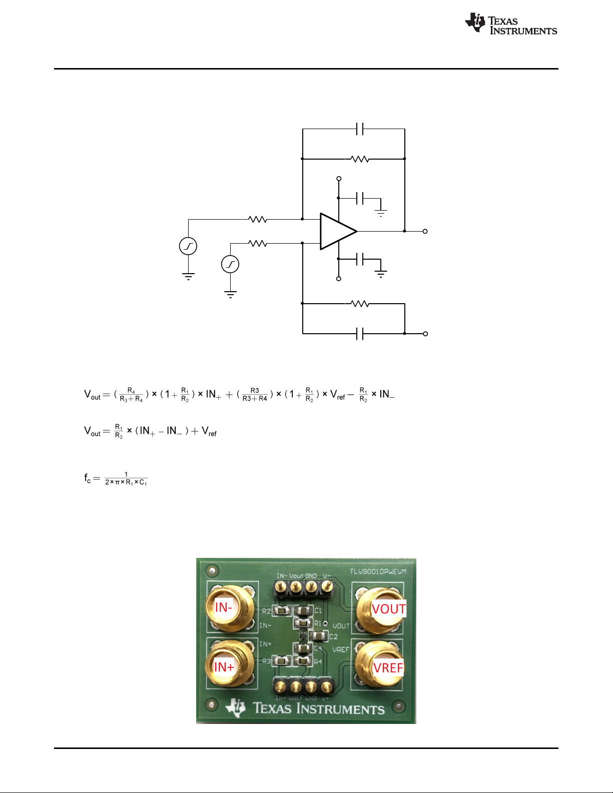
4 Schematic and PCB Layout
This section provides the schematic and PCB layout of the TLV9001DPW EVM. Also included are the
schematics for the three TLV9001DPW EVM circuit configuration options.
4.1 Schematic
Figure 1 displays the circuit schematic of the TLV9001DPW EVM.
Schematic and PCB Layout
Figure 1. TLV9001DPW EVM Schematic
The schematic of the EVM is provided in silk screen located on the back of the PCB for easy reference.
Figure 2 displays the schematic provided on the back of the PCB.
Figure 2. Silkscreen Schematic
SLOU512–October 2018
Submit Documentation Feedback
Copyright © 2018, Texas Instruments Incorporated
TLV9001DPW-EVM
3
Page 4
-
+
V+
C2
C1
R1
C3
C4
R4
R2
R3
IN+
VOUT
VREF
V-
Schematic and PCB Layout
4.2 Difference Amplifier
Figure 3 displays the schematic for the difference amplifier circuit configuration.
www.ti.com
Figure 3. Difference Amplifier Schematic
Equation 1 displays the transfer function of the difference amplifier circuit configuration.
If R1 = R4 and R2 = R3, Equation 1 can simplify to Equation 2.
Capacitors C1 and C4 provide the option to filter the output of the amplifier. Equation 3 calculates the
cutoff frequency, fc, of the filter.
Where
• R1 = R4, R2 = R3, and C1 = C4
Figure 4 displays the TLV9001DPW EVM populated with the required components to be configured as a
difference amplifier.
(1)
(2)
(3)
4
TLV9001DPW-EVM
Figure 4. Difference Amplifier Configured on TLV9001DPW EVM
Copyright © 2018, Texas Instruments Incorporated
SLOU512–October 2018
Submit Documentation Feedback
Page 5

-
+
V+
C2
C1
R1
C3
R2
IN+
VOUT
V-
www.ti.com
4.3 Non-Inverting Amplifier
Figure 5 displays the schematic for the non-inverting amplifier circuit configuration. To configure the EVM
in a non-inverting configuration short R3 using a 0-Ω resistor or solder bridge, leave R4 and C4
unpopulated, and ground the input connection IN–. The input signal is applied directly to the high
impedance non-inverting input terminal using the IN+ connection on the EVM.
Schematic and PCB Layout
Figure 5. Non-Inverting Amplifier Schematic
Equation 4 displays the DC transfer function of the non-inverting amplifier circuit configuration shown in
Figure 5.
Capacitor C1 provides the option to filter the output. The cutoff frequency, fc, of the filter can be calculated
using Equation 5.
Figure 6 displays the TLV9001DPW EVM populated with the required components to be configured as a
non-inverting amplifier.
Figure 6. Non-Inverting Amplifier Configured on TLV9001DPW EVM
(4)
(5)
SLOU512–October 2018
Submit Documentation Feedback
Copyright © 2018, Texas Instruments Incorporated
TLV9001DPW-EVM
5
Page 6

-
+
V+
C2
C1
R1
C3
R2
VOUT
V-
Vcm
Schematic and PCB Layout
4.4 Inverting Amplifier
Figure 7 shows the schematic for the inverting amplifier circuit configuration. To configure the EVM in an
inverting configuration short R3 using a 0-Ω resistor or solder bridge, leave R4 and C4 unpopulated, and
apply the desired common mode voltage to the input connection, IN+. The input signal is applied using the
input connection IN–.
www.ti.com
Figure 7. Inverting Amplifier Schematic
Equation 6 displays the DC transfer function of the inverting amplifier circuit configuration.
Capacitor C1 provides the option to filter the output. The cutoff frequency, fc, of the filter can be calculated
using Equation 7.
Figure 8 shows the TLV9001DPW EVM populated with the required components to be configured as an
inverting amplifier.
Figure 8. Inverting Amplifier Configured on TLV9001DPW EVM
(6)
(7)
6
TLV9001DPW-EVM
Copyright © 2018, Texas Instruments Incorporated
SLOU512–October 2018
Submit Documentation Feedback
Page 7

www.ti.com
4.5 PCB Layout
The TLV9001DPW EVM is a two layer board. The PCB layout of the top layer is displayed in Figure 9.
Schematic and PCB Layout
Figure 9. Top Layer PCB Layout
The PCB layout of the bottom layer is displayed in Figure 10.
Figure 10. Bottom Layer PCB Layout
SLOU512–October 2018
Submit Documentation Feedback
Copyright © 2018, Texas Instruments Incorporated
TLV9001DPW-EVM
7
Page 8
Connections
5 Connections
This section provides a description for each connection available on the EVM.
5.1 Power
The power supply connections for the TLV9001DPW EVM can only be applied using the header strips
located at the top and bottom of the PCB. The positive power supply connection is labeled V+, the
negative power supply connection is labeled V–, and the ground connection is labeled GND. For the
minimum and maximum supply voltages of the TLV9001DPW EVM, please refer to the TLV9001 product
datasheet (SBOS833).
5.2 Input Connections
Signals for the input can be applied to the TLV9001DPW EVM through the use of SMA connectors or the
header pins. The input connections are labeled as IN+ and IN–.
5.3 Output Connections
Output connections are provided through the use of SMA connectors or the header pin labeled as VOUT.
5.4 Reference Voltage Connections
Signals or DC voltages for the reference voltage is applied to the TLV9001DPW EVM through the use of
the SMA connector or header pin labeled VREF.
www.ti.com
6 Bill of Materials and References
6.1 Bill of Materials
Designator QTY Description Part Number
PCB 1 Printed-Circuit-Board TLV9001DPW EVM
Header Strips 2 Header, 100 mil, 4x1, Gold, TH TS-104-G-AA
6.2 References
1. DIYAMP-EVM
2. DUAL-DIYAMP-EVM
3. TI Precision Labs Training
8
TLV9001DPW-EVM
Copyright © 2018, Texas Instruments Incorporated
SLOU512–October 2018
Submit Documentation Feedback
Page 9

IMPORTANT NOTICE AND DISCLAIMER
TI PROVIDES TECHNICAL AND RELIABILITY DATA (INCLUDING DATASHEETS), DESIGN RESOURCES (INCLUDING REFERENCE
DESIGNS), APPLICATION OR OTHER DESIGN ADVICE, WEB TOOLS, SAFETY INFORMATION, AND OTHER RESOURCES “AS IS”
AND WITH ALL FAULTS, AND DISCLAIMS ALL WARRANTIES, EXPRESS AND IMPLIED, INCLUDING WITHOUT LIMITATION ANY
IMPLIED WARRANTIES OF MERCHANTABILITY, FITNESS FOR A PARTICULAR PURPOSE OR NON-INFRINGEMENT OF THIRD
PARTY INTELLECTUAL PROPERTY RIGHTS.
These resources are intended for skilled developers designing with TI products. You are solely responsible for (1) selecting the appropriate
TI products for your application, (2) designing, validating and testing your application, and (3) ensuring your application meets applicable
standards, and any other safety, security, or other requirements. These resources are subject to change without notice. TI grants you
permission to use these resources only for development of an application that uses the TI products described in the resource. Other
reproduction and display of these resources is prohibited. No license is granted to any other TI intellectual property right or to any third
party intellectual property right. TI disclaims responsibility for, and you will fully indemnify TI and its representatives against, any claims,
damages, costs, losses, and liabilities arising out of your use of these resources.
TI’s products are provided subject to TI’s Terms of Sale (www.ti.com/legal/termsofsale.html) or other applicable terms available either on
ti.com or provided in conjunction with such TI products. TI’s provision of these resources does not expand or otherwise alter TI’s applicable
warranties or warranty disclaimers for TI products.
Mailing Address: Texas Instruments, Post Office Box 655303, Dallas, Texas 75265
Copyright © 2018, Texas Instruments Incorporated
 Loading...