

TLV821 SINGLE/TLV822 DUAL/TLV824 QUAD
OPERATIONAL AMPLIFIERS
SLOS296A – FEBRUARY 2000 – REVISED MAY 2000
1
POST OFFICE BOX 655303 • DALLAS, TEXAS 75265
D
2.7-V and 5-V Performance
D
No Crossover Distortion
D
Low Supply Current at V
CC+
= 5 V:
TLV821 . . . 0.3 mA Typ
TL V822 . . . 0.5 mA Typ
TL V824 ...1 mA Typ
D
Rail-to-Rail Output Swing
D
Pin-to-Pin Compatible with LMV821,
LMV822, and LMV824 Devices
D
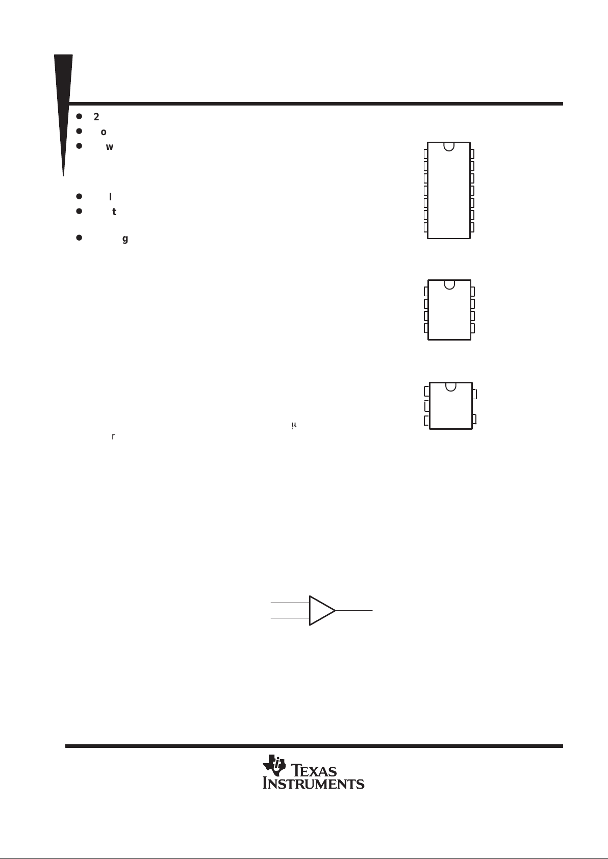
Package Options Include Plastic
Small-Outline (D), Small-Outline Transistor
(SOT-23 DBV, SC-70 DCK), and Thin Shrink
Small-Outline (PW) Packages
description
The TLV821, TLV822, and TLV824 devices are
low-voltage (2.5 V to 5.5 V) low-power operational
amplifiers, designed to be functionally and
pin-to-pin compatible with the LMV821, LMV822,
and LMV824 devices. Electrical characteristics
are very similar to the LMV3xx operational
amplifiers (low supply current, rail-to-rail outputs,
input common-mode range, which includes
ground). The TLV8xx devices have a significantly
higher bandwidth (8 MHz typically) and a 2.5-V/ms
slew rate. The TLV821 is a single, the TLV822 is
a dual, and the TLV824 is a quad operational
amplifier.
These devices are the most cost-effective solution for applications requiring low-voltage/low-power operation
and space-saving considerations. The TLV821 is available in the ultra-small DCK package, which is
approximately half the size of the DBV package. The DCK package saves space on PC boards and enables
the design of small portable electronic devices (cordless and cellular phones, laptops, PDAs, PCMIAs). It also
allows the designer to place the device closer to the signal source to reduce noise pickup and increase signal
integrity .
The TLV821I, TLV822I, and TLV824I devices are characterized for operation from –40°C to 85°C.
symbol (each amplifier)
OUT
IN–
IN+
_
+
PRODUCT PREVIEW
Copyright 2000, Texas Instruments Incorporated
1
2
3
4
5
6
7
14
13
12
11
10
9
8
1OUT
1IN–
1IN+
V
CC+
2IN+
2IN–
2OUT
4OUT
4IN–
4IN+
GND
3IN+
3IN–
3OUT
TLV824...D OR PW PACKAGE
(TOP VIEW)
TLV822...D OR PW PACKAGE
(TOP VIEW)
1
2
3
4
8
7
6
5
1OUT
1IN –
1IN+
GND
V
CC+
2OUT
2IN –
2IN+
TLV821. . . DBV OR DCK PACKAGE
(TOP VIEW)
V
CC+
1
2
3
5
4
IN+
GND
IN–
OUT
PRODUCT PREVIEW information concerns products in the formative or
design phase of development. Characteristic data and other
specifications are design goals. Texas Instruments reserves the right to
change or discontinue these products without notice.
TLV821 SINGLE/TLV822 DUAL/TLV824 QUAD
OPERATIONAL AMPLIFIERS
SLOS296A – FEBRUARY 2000 – REVISED MAY 2000
2
POST OFFICE BOX 655303 • DALLAS, TEXAS 75265
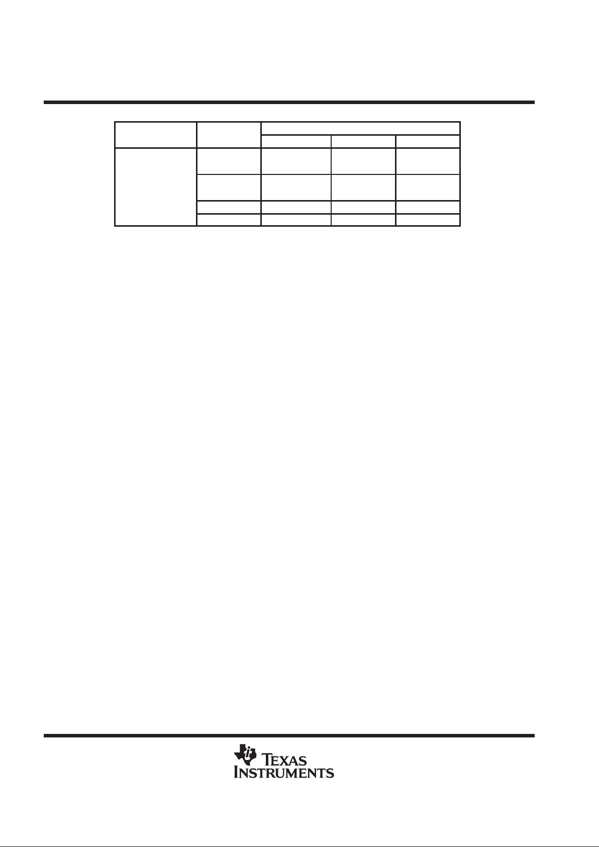
AVAILABLE OPTIONS
PACKAGE
PACKAGED DEVICES
T
A
TYPE
SINGLE DUAL QUADRUPLE
p
TLV821IDCKR — —
5-pin SOT
TLV821IDBVR — —
–40°C to 85°C
8-pin SOIC — TLV822ID —
8-pin TSSOP — TLV822IPWR —
14-pin SOIC — — TLV824ID
14-pin TSSOP — — TLV824IPWR
The D package is available taped and reeled. Add the suffix R to the device type (e.g., TL V824IDR).
The DCK, DBV, and PW packages are only available left-end taped and reeled.
absolute maximum ratings over operating free-air temperature range (unless otherwise noted)
†
Supply voltage, VCC (see Note 1) 5.5 V. . . . . . . . . . . . . . . . . . . . . . . . . . . . . . . . . . . . . . . . . . . . . . . . . . . . . . . . . . .
Differential input voltage, V
ID
(see Note 2) ±5.5 V. . . . . . . . . . . . . . . . . . . . . . . . . . . . . . . . . . . . . . . . . . . . . . . . . .
Input voltage range, VI (either input) 0 to 5.5 V. . . . . . . . . . . . . . . . . . . . . . . . . . . . . . . . . . . . . . . . . . . . . . . . . . . . .
Duration of output short circuit (one amplifier) to ground at (or below) T
A
= 25°C,
VCC ≤ 5.5 V (see Note 3) Unlimited. . . . . . . . . . . . . . . . . . . . . . . . . . . . . . . . . . . . . . . . . . . . . . . . . . . . . . . . . . . . .
Operating virtual junction temperature 150°C. . . . . . . . . . . . . . . . . . . . . . . . . . . . . . . . . . . . . . . . . . . . . . . . . . . . . .
Package thermal impedance, θ
JA
(see Notes 4 and 5): D (8-pin) package 97°C/W. . . . . . . . . . . . . . . . . . . . . .
D (14-pin) package 86°C/W. . . . . . . . . . . . . . . . . . . .
DBV package 347°C/W. . . . . . . . . . . . . . . . . . . . . . . .
DCK package 389°C/W. . . . . . . . . . . . . . . . . . . . . . . .
PW (8-pin) package 149°C/W. . . . . . . . . . . . . . . . . . .
PW (14-pin) package 113°C/W. . . . . . . . . . . . . . . . . .
Lead temperature 1,6 mm (1/16 inch) from case for 10 seconds: D or PW package 260°C. . . . . . . . . . . . . .
Storage temperature range, T
stg
–65 to 150°C. . . . . . . . . . . . . . . . . . . . . . . . . . . . . . . . . . . . . . . . . . . . . . . . . . . . .
†
Stresses beyond those listed under “absolute maximum ratings” may cause permanent damage to the device. These are stress ratings only, and
functional operation of the device at these or any other conditions beyond those indicated under “recommended operating conditions” is not
implied. Exposure to absolute-maximum-rated conditions for extended periods may affect device reliability.
NOTES: 1. All voltage values (except differential voltages and VCC specified for the measurement of IOS) are with respect to the network GND.
2. Differential voltages are at IN+ with respect to IN–.
3. Short circuits from outputs to VCC can cause excessive heating and eventual destruction.
4. Maximum power dissipation is a function of TJ(max), θJA, and TA. The maximum allowable power dissipation at any allowable
ambient temperature is PD = (TJ(max) – TA)/θJA. Selecting the maximum of 150°C can affect reliability.
5. The package thermal impedance is calculated in accordance with JESD 51.
PRODUCT PREVIEW
TLV821 SINGLE/TLV822 DUAL/TLV824 QUAD
OPERATIONAL AMPLIFIERS
SLOS296A – FEBRUARY 2000 – REVISED MAY 2000
3
POST OFFICE BOX 655303 • DALLAS, TEXAS 75265
recommended operating conditions
MIN MAX UNIT
V
CC
Supply voltage (single-supply operation) 2.5 5.5 V
T
A
Operating free-air temperature –40 85 °C
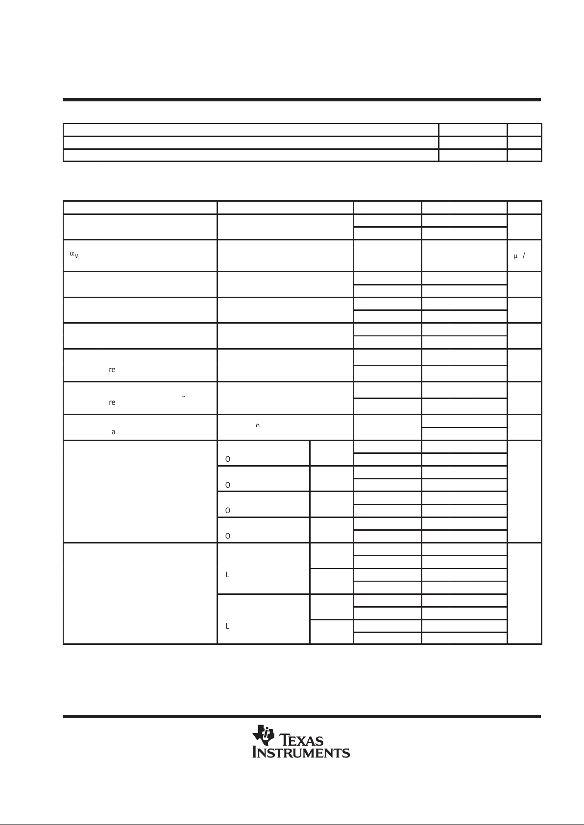
electrical characteristics at specified free-air temperature, V
CC+
= 2.7 V,
GND= 0 V, V
CM
= 1 V, VO = 1.35 V, and RL > 1 MΩ (unless otherwise noted)
PARAMETER
TEST CONDITIONS T
A
MIN TYP MAX UNIT
p
25°C 1 3.5
VIOInput offset voltage
–40°C to 85°C 4
mV
a
V
IO
Average temperature
coefficient of input offset
voltage
25°C 1
m
V/°C
p
25°C 30 90
IIBInput bias current
–40°C to 85°C 140
nA
p
25°C 0.5 30
IIOInput offset current
–40°C to 85°C 50
nA
25°C 60 73
CMRR
Common-mode rejection ratio
V
CM
= 0 to 1.7
V
–40°C to 85°C 58
dB
Positive supply-voltage
V
CC+
= 1.7 V to 4 V,
25°C 60 75
+
k
SVR
yg
rejection ratio
GND
= 1 V,
VCM = 0, VO = 0
–40°C to 85°C 58
dB
Negative supply-voltage
V
CC+
= 1.7 V,
25°C 60 75
–
k
SVR
gyg
rejection ratio
GND
= –1 V to –3.3 V,
VCM = 0, VO = 0
–40°C to 85°C 58
dB
Common-mode input voltage
°
–0.2 –0.3
V
ICR
g
range
CMRR ≥ 50 dB
25°C
1.9 2
V
R
= 600 Ω to 1.35 V ,
25°C 90 100
L
,
VO = 1.35 V to 2.2 V
Sourcing
–40°C to 85°C 85
R
= 600 Ω to 1.35 V ,
25°C 85 90
Large-signal
L
,
VO = 1.35 V to 0.5 V
Sinking
–40°C to 85°C 80
A
VD
diff
erential-voltage
a
mplification
R
= 2 kΩ to 1.35 V,
25°C 95 100
dB
am lification
L
,
VO = 1.35 V to 2.2 V
Sourcing
–40°C to 85°C 90
R
= 2 kΩ to 1.35 V,
25°C 90 95
L
,
VO = 1.35 V to 0.5 V
Sinking
–40°C to 85°C 85
25°C 2.5 2.58
V
= 2.7 V,
High level
–40°C to 85°C 2.4
CC+
,
RL = 600 Ω to 1.35 V
25°C 0.13 0.2
p
Low level
–40°C to 85°C 0.3
Output swing
25°C 2.6 2.66
V
V
= 2.7 V,
High level
–40°C to 85°C 2.5
CC+
,
RL = 2 kΩ to 1.35 V
25°C 0.08 0.12
Low level
–40°C to 85°C 0.2
PRODUCT PREVIEW

TLV821 SINGLE/TLV822 DUAL/TLV824 QUAD
OPERATIONAL AMPLIFIERS
SLOS296A – FEBRUARY 2000 – REVISED MAY 2000
4
POST OFFICE BOX 655303 • DALLAS, TEXAS 75265
electrical characteristics at specified free-air temperature, V
CC+
= 2.7 V,
GND = 0 V, V
CM
= 1 V, VO = 1.35 V, and RL > 1 MΩ (unless otherwise noted) (continued)
PARAMETER
TEST CONDITIONS T
A
MIN TYP MAX UNIT
p
VO = 0 V Sourcing 25°C 12 16
IOOutput current
VO = 2.7 V Sinking 25°C 12 26
mA
25°C 0.22 0.3
TLV821I
–40°C to 85°C 0.5
pp
p
25°C 0.45 0.6
ICCSupply current
TLV822I (both amplifiers)
–40°C to 85°C 0.8
mA
p
25°C 0.72 1
TLV824I (all four amplifiers)
–40°C to 85°C 1.2
SR Slew rate V
CC+
= 5 V
†
25°C 2 V/ms
GBM Gain-bandwidth product 25°C 7 MHz
f
m
Phase margin 25°C 61 deg
G
m
Gain margin 25°C 10 dB
Amplifier-to-amplifier isolation V
CC+
= 5 V, RL = 100 kΩ to 2.5 V
‡
25°C 135 dB
V
n
Equivalent input noise voltage f = 1 kHz, VCM = 1 V 25°C 28 nV/√Hz
I
n
Equivalent input noise voltage f = 1 kHz 25°C 0.1 pA/√Hz
THD Total harmonic distortion
f = 1 kHz,
AVD = –2, RL = 10 kΩ, VO = 4.1 V
PP
25°C 0.01%
†
Connected as voltage follower with 3-V step input. Value specified is the slower of the positive and negative slew rates.
‡
Refers to inputs only. Each amplifier is excited, in turn, with 1 kHz to produce VO = 3 VPP.
PRODUCT PREVIEW

TLV821 SINGLE/TLV822 DUAL/TLV824 QUAD
OPERATIONAL AMPLIFIERS
SLOS296A – FEBRUARY 2000 – REVISED MAY 2000
5
POST OFFICE BOX 655303 • DALLAS, TEXAS 75265
electrical characteristics at specified free-air temperature, V
CC+
= 5 V,
GND= 0 V, V
CM
= 2 V, VO = 2.5 V, and RL > 1 MΩ (unless otherwise noted)
PARAMETER
TEST CONDITIONS T
A
MIN TYP MAX UNIT
p
25°C 1 3.5
VIOInput offset voltage
–40°C to 85°C 4
mV
a
V
IO
Average temperature
coefficient of input offset
voltage
25°C 1
m
V/°C
p
25°C 40 100
IIBInput bias current
–40°C to 85°C 150
nA
p
25°C 0.5 30
IIOInput offset current
–40°C to 85°C 50
nA
Common-mode rejection
25°C 62 75
CMRR
j
ratio
V
CM
= 0 to 4
V
–40°C to 85°C 60
dB
Positive supply-voltage
V
CC+
= 1.7 V to 4 V,
25°C 60 75
+
k
SVR
yg
rejection ratio
GND
= –1 V,
VCM = 0, VO = 0
–40°C to 85°C 58
dB
Negative supply-voltage
V
CC+
= 1.7 V,
25°C 60 75
–
k
SVR
gyg
rejection ratio
GND
= –1 V to –3.3 V,
VCM = 0, VO = 0
–40°C to 85°C 58
dB
Common-mode input
°
–0.2 –0.3
V
ICR
voltage range
CMRR ≥ 50 dB
25°C
4.2 4.3
V
R
= 600 Ω to 2.5 V ,
25°C 95 105
L
,
VO = 2.5 V to 4.5 V
Sourcing
–40°C to 85°C 90
R
= 600 Ω to 2.5 V ,
25°C 95 105
Large-signal
L
,
VO = 2.5 V to 0.5 V
Sinking
–40°C to 85°C 90
A
VD
diff
erential-voltage
amplification
R
= 2 kΩ to 2.5 V,
25°C 95 105
dB
am lification
L
,
VO = 2.5 V to 4.5 V
Sourcing
–40°C to 85°C 90
R
= 2 kΩ to 2.5 V,
25°C 95 105
L
,
VO = 2.5 V to 0.5 V
Sinking
–40°C to 85°C 90
25°C 4.75 4.84
V
= 5 V,
High level
–40°C to 85°C 4.7
CC+
,
RL = 600 Ω to 2.5 V
25°C 0.17 0.25
p
Low level
–40°C to 85°C 0.3
Output swing
25°C 4.85 4.9
V
V
= 5 V,
High level
–40°C to 85°C 4.8
CC+
,
RL = 2 kΩ to 2.5 V
25°C 0.1 0.15
Low level
–40°C to 85°C 0.2
25°C 20 45
p
V
O
=
0 V
Sourcing
–40°C to 85°C 15
IOOutput current
25°C 20 40
mA
V
O
=
5 V
Sinking
–40°C to 85°C 15
PRODUCT PREVIEW

TLV821 SINGLE/TLV822 DUAL/TLV824 QUAD
OPERATIONAL AMPLIFIERS
SLOS296A – FEBRUARY 2000 – REVISED MAY 2000
6
POST OFFICE BOX 655303 • DALLAS, TEXAS 75265
electrical characteristics at specified free-air temperature, V
CC+
= 5 V,
GND = 0 V, V
CM
= 2 V, VO = 2.5 V, and RL > 1 MΩ (unless otherwise noted) (continued)
PARAMETER
TEST CONDITIONS T
A
MIN TYP MAX UNIT
25°C 0.3 0.4
TLV821I
–40°C to 85°C 0.6
pp
p
25°C 0.5 0.7
ICCSupply current
TLV822I (both amplifiers)
–40°C to 85°C 0.9
mA
p
25°C 1 1.3
TLV824I (all four amplifiers)
–40°C to 85°C 1.5
SR Slew rate V
CC+
= 5 V
†
25°C 2 2.5 V/ms
GBM Gain-bandwidth product 25°C 8 MHz
f
m
Phase margin 25°C 67 deg
G
m
Gain margin 25°C 15 dB
Amplifier-to-amplifier isolation V
CC+
= 5 V, RL = 100 kΩ to 2.5 V
‡
25°C 135 dB
V
n
Equivalent input noise voltage f = 1 kHz, VCM = 1 V 25°C 24 nV/√Hz
I
n
Equivalent input noise voltage f = 1 kHz 25 °C 0.25 pA/√Hz
THD T otal harmonic distortion
f = 1 kHz,
AVD = –2, RL = 10 kΩ, VO = 4.1 V
PP
25°C 0.01%
†
Connected as voltage follower with 3-V step input. Value specified is the slower of the positive and negative slew rates.
‡
Refers to inputs only. Each amplifier is excited, in turn, with 1 kHz to produce VO = 3 VPP.
PRODUCT PREVIEW

IMPORTANT NOTICE
T exas Instruments and its subsidiaries (TI) reserve the right to make changes to their products or to discontinue
any product or service without notice, and advise customers to obtain the latest version of relevant information
to verify, before placing orders, that information being relied on is current and complete. All products are sold
subject to the terms and conditions of sale supplied at the time of order acknowledgment, including those
pertaining to warranty, patent infringement, and limitation of liability.
TI warrants performance of its semiconductor products to the specifications applicable at the time of sale in
accordance with TI’s standard warranty. Testing and other quality control techniques are utilized to the extent
TI deems necessary to support this warranty. Specific testing of all parameters of each device is not necessarily
performed, except those mandated by government requirements.
Customers are responsible for their applications using TI components.
In order to minimize risks associated with the customer’s applications, adequate design and operating
safeguards must be provided by the customer to minimize inherent or procedural hazards.
TI assumes no liability for applications assistance or customer product design. TI does not warrant or represent
that any license, either express or implied, is granted under any patent right, copyright, mask work right, or other
intellectual property right of TI covering or relating to any combination, machine, or process in which such
semiconductor products or services might be or are used. TI’s publication of information regarding any third
party’s products or services does not constitute TI’s approval, warranty or endorsement thereof.
Copyright 2000, Texas Instruments Incorporated
 Loading...