

Page 1
www.ti.com
FEATURES APPLICATIONS
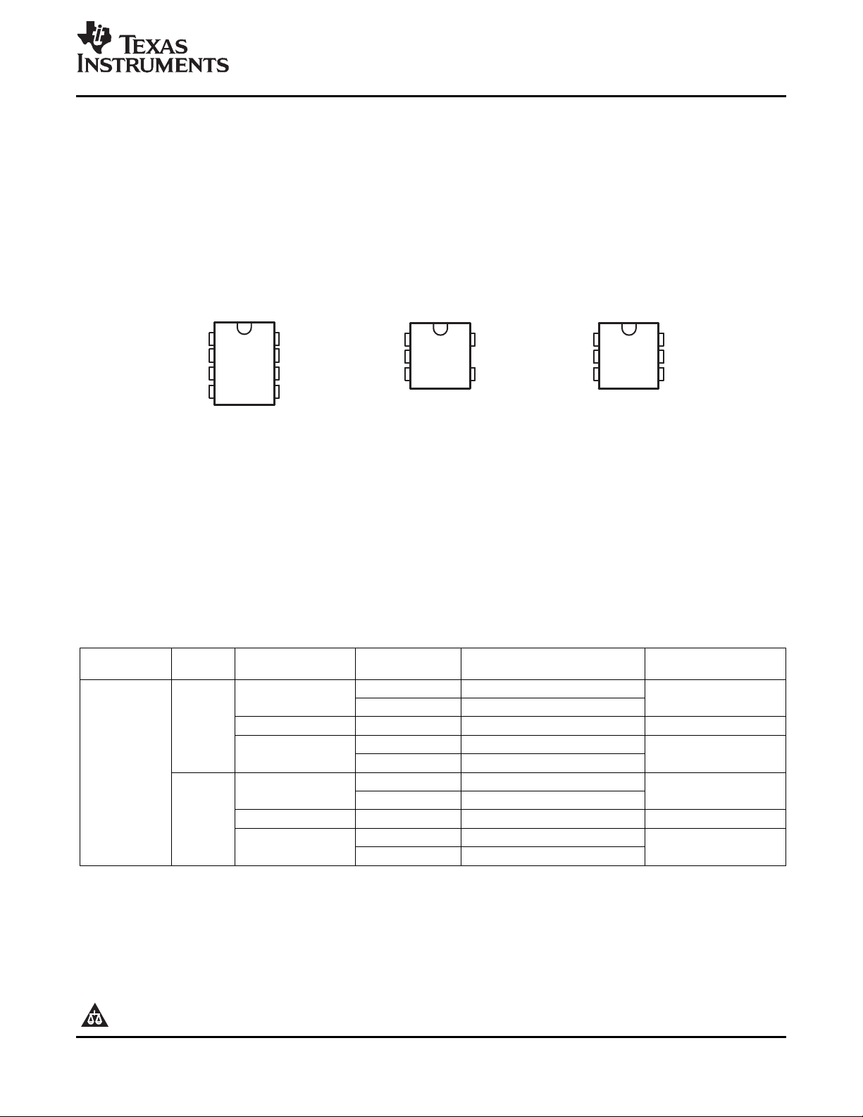
D PACKAGE
(TOPVIEW)
1
2
3
4
8
7
6
5
NC
V
CC+
OUT
NC
NC
IN–
IN+
V
CC–
NC – No internal connection
DBV PACKAGE
(TOPVIEW)
1
2
3
5
4
OUT
V
CC+
IN+
V
CC–
IN–
DCK PACKAGE
(TOPVIEW)
1
2
3
6
4
OUT
V
CC+
IN+
NC
IN–
5
V
CC–
• Parameters Specified at 2.7-V, 5-V, and 15-V
Supplies
• Supply Current 7 µ A (Typ) at 5 V
• Response Time 4 µ s (Typ) at 5 V
• Push-Pull Output
• Input Common-Mode Range Beyond
V
and V
CC–
• Low Input Current
CC+
TLV7211 , , TLV7211A
CMOS COMPARATORS
WITH RAIL-TO-RAIL INPUT AND PUSH-PULL OUTPUT
SLCS149B – AUGUST 2006 – REVISED JANUARY 2007
• Battery-Powered Products
• Notebooks and PDAs
• Mobile Communications
• Alarm and Security Circuits
• Direct Sensor Interface
• Replaces Amplifiers Used as Comparators
With Better Performance and Lower Current
DESCRIPTION/ORDERING INFORMATION
The TLV7211 and TLV7211A are micropower CMOS comparators available in the space-saving SOT-23-5
package. This makes the comparators ideal for space- and weight-critical designs. The TLV7211A features an
input offset voltage of 5 mV, and the TLV7211 features an input offset voltage of 15 mV.
The main benefits of the SOT-23-5 package are most apparent in small portable electronic devices, such as
mobile phones, pagers, notebook computers, personal digital assistants, and PCMCIA cards. The rail-to-rail
input voltage makes the TLV7211 or TLV7211A a good choice for sensor interfacing, such as light detector
circuits, optical and magnetic sensors, and alarm and status circuits.
The SOT-23-5 package's small size allows it to fit into tight spaces on PC boards.
ORDERING INFORMATION
V
T
A
–40 ° C to 85 ° C
(1) Package drawings, standard packing quantities, thermal data, symbolization, and PCB design guidelines are available at
www.ti.com/sc/package.
(2) DBV/DCK: The actual top-side marking has one additional character that designates the assembly/test site.
OS
(MAX)
5 mV SOT-23-5 – DBV Reel of 3000 TLV7211AIDBVR YBN_
15 mV SOT-23-5 – DBV Reel of 3000 TLV7211IDBVR YBK_
PACKAGE
SOIC – D 7211AI
SOT (SC-70) – DCK Y8_
SOIC – D TY7211
SOT (SC-70) – DCK Y7_
(1)
Reel of 2500 TLV7211AIDR
Tube of 75 TLV7211AID
Reel of 3000 TLV7211AIDCKR
Reel of 250 TLV7211AIDCKT
Reel of 2500 TLV7211IDR
Tube of 75 TLV7211ID
Reel of 3000 TLV7211IDCKR
Reel of 250 TLV7211IDCKT
ORDERABLE PART NUMBER TOP-SIDE MARKING
(2)
PRODUCTION DATA information is current as of publication date.
Products conform to specifications per the terms of the Texas
Instruments standard warranty. Production processing does not
necessarily include testing of all parameters.
Please be aware that an important notice concerning availability, standard warranty, and use in critical applications of Texas Instruments semiconductor products and disclaimers thereto appears at the end of this data sheet.
Copyright © 2006–2007, Texas Instruments Incorporated
Page 2
www.ti.com
IN–
IN+
OUT
TLV7211 , , TLV7211A
CMOS COMPARATORS
WITH RAIL-TO-RAIL INPUT AND PUSH-PULL OUTPUT
SLCS149B – AUGUST 2006 – REVISED JANUARY 2007
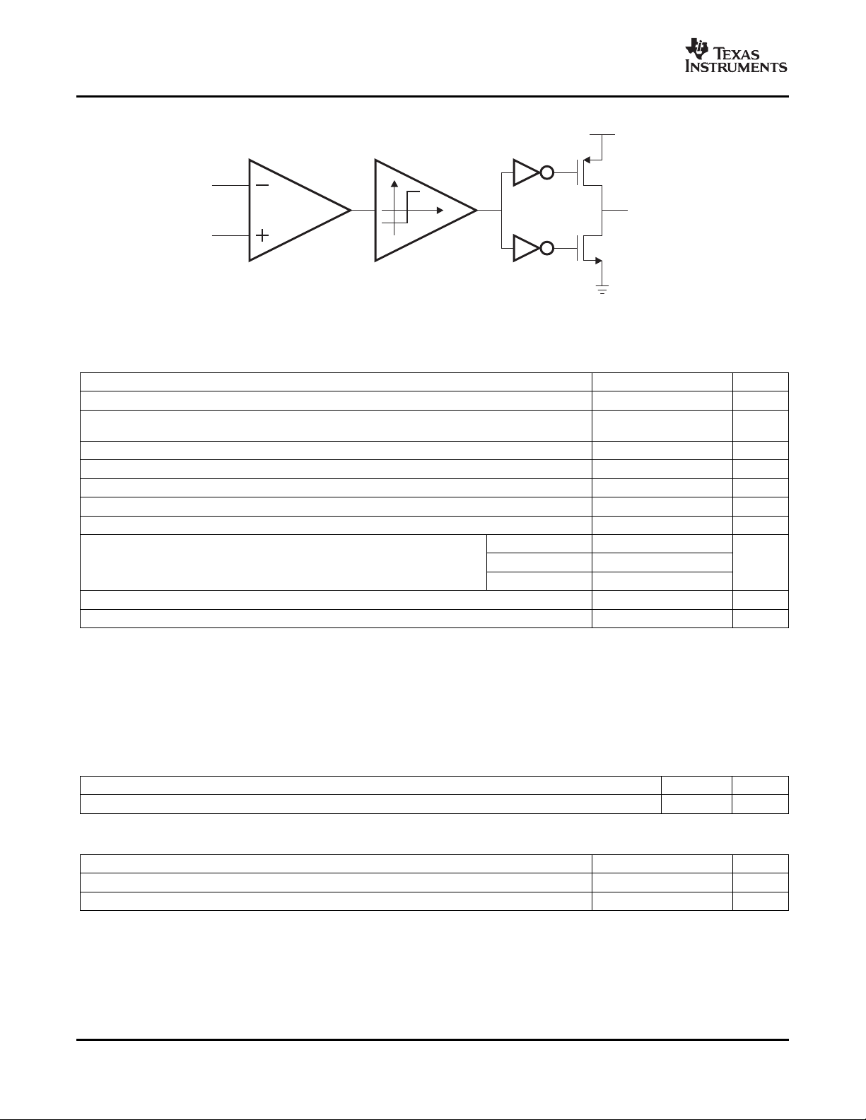
FUNCTIONAL BLOCK DIAGRAM
Absolute Maximum Ratings
(1)
over operating free-air temperature range (unless otherwise noted)
MIN MAX UNIT
V
– V
CC+
CC–
V
ID
V
I
V
O
I
CC
I
I
I
O
θ
JA
T
J
T
stg
Supply voltage
Differential input voltage
Input voltage range (any input) V
Output voltage range V
Supply current 40 mA
Input current ± 5 mA
Output current ± 30 mA
Package thermal impedance
Operating virtual junction temperature 150 ° C
Storage temperature range –65 150 ° C
(1) Stresses beyond those listed under "absolute maximum ratings" may cause permanent damage to the device. These are stress ratings
only, and functional operation of the device at these or any other conditions beyond those indicated under "recommended operating
conditions" is not implied. Exposure to absolute-maximum-rated conditions for extended periods may affect device reliability.
(2) All voltage values (except differential voltages and V
(3) Differential voltages are at IN+ with respect to IN–.
(4) Maximum power dissipation is a function of TJ(max), θJA, and TA. The maximum allowable power dissipation at any allowable ambient
temperature is PD= (TJ(max) – TA)/ θJA. Operating at the absolute maximum TJof 150 ° C can affect reliability.
(5) The package thermal impedance is calculated in accordance with JESD 51-7.
(2)
(3)
– 0.3 V
CC–
– 0.3 V
CC–
± Supply
voltage
CC+
CC+
+ 0.3 V
+ 0.3 V
D package 97
(4) (5)
DBV package 206 ° C/W
DCK package 259
specified for the measurement of IOS) are with respect to the network GND.
CC
16 V
V
ESD Protection
TYP UNIT
Human-Body Model 2000 V
Recommended Operating Conditions
MIN MAX UNIT
V
– V
CC+
CC–
T
J
2
Supply voltage 2.7 15 V
Operating virtual junction temperature –40 85 ° C
Submit Documentation Feedback
Page 3
www.ti.com
TLV7211 , , TLV7211A
CMOS COMPARATORS
WITH RAIL-TO-RAIL INPUT AND PUSH-PULL OUTPUT
SLCS149B – AUGUST 2006 – REVISED JANUARY 2007
2.7-V Electrical Characteristics
V
= 2.7 V, V
CC+
PARAMETER TEST CONDITIONS T
V
OS
TCV
Input offset voltage mV
Input offset voltage
OS
temperature drift
Input offset voltage
average drift
I
B
I
OS
CMRR 0 ≤ V
PSRR 2.7 V ≤ V
A
V
CMVR V
V
OH
V
OL
I
CC
Input current 25 ° C 0.04 0.04 pA
Input offset current 25 ° C 0.02 0.02 pA
Common-mode
rejection ratio
Power-supply rejection
ratio
Voltage gain 25 ° C 100 100 dB
Input common-mode
voltage range
High-level output
voltage
Low-level output
voltage
Supply current µ A
(1) Input offset voltage average drift is calculated by dividing the accelerated operating life V
represents worst-case input conditions and includes the first 30 days of drift.
CC–
= GND, V
(1)
CM
= VO= V
/2, and RL> 1 M Ω (unless otherwise noted)
CC+
TLV7211A TLV7211
J
MIN TYP MAX MIN TYP MAX
25 ° C 3 5 3 15
–40 ° C to 85 ° C 8 18
25 ° C 1 1 µ V/ ° C
25 ° C 3.3 3.3 µ V/month
≤ 2.7 V 25 ° C 75 75 dB
CM
≤ 15 V 25 ° C 80 80 dB
CC+
CMRR > 55 dB
CMRR > 55 dB
I
= 2.5 mA V
load
I
= 2.5 mA V
load
V
= Low
OUT
V
= High-Idle
OUT
25 ° C 2.9 3 2.9 3
–40 ° C to 85 ° C 2.7 2.7
25 ° C –0.3 –0.2 –0.3 –0.2
–40 ° C to 85 ° C 0 0
25 ° C 2.4 2.5 2.4 2.5
–40 ° C to 85 ° C 2.3 2.3
25 ° C 0.2 0.3 0.2 0.3
–40 ° C to 85 ° C 0.4 0.4
25 ° C 7 12 7 12
–40 ° C to 85 ° C 14 14
25 ° C 5 10 5 10
–40 ° C to 85 ° C 12 12
drift by the equivalent operational time. This
OS
UNIT
Submit Documentation Feedback
3
Page 4
www.ti.com
TLV7211 , , TLV7211A
CMOS COMPARATORS
WITH RAIL-TO-RAIL INPUT AND PUSH-PULL OUTPUT
SLCS149B – AUGUST 2006 – REVISED JANUARY 2007
5-V Electrical Characteristics
V
= 5 V, V
CC+
V
OS
TCV
OS
I
B
I
OS
CMRR 25 ° C 75 75 dB
PSRR 5 V ≤ V
A
V
CMVR V
V
OH
V
OL
I
CC
I
OH
I
OL
(1) Input offset voltage average drift is calculated by dividing the accelerated operating life V
represents worst-case input conditions and includes the first 30 days of drift.
(2) Do not short circuit the output to V+ if V+ is >12 V.
= GND, V
CC–
PARAMETER TEST CONDITIONS T
Input offset voltage mV
Input offset voltage
temperature drift
Input offset voltage
average drift
(1)
CM
= VO= V
/2, and RL> 1 M Ω (unless otherwise noted)
CC+
J
25 ° C 3 5 3 15
–40 ° C to 85 ° C 8 18
25 ° C 1 1 µ V/ ° C
25 ° C 3.3 3.3 µ V/month
TLV7211A TLV7211
MIN TYP MAX MIN TYP MAX
Input current 25 ° C 0.04 0.04 pA
Input offset current 25 ° C 0.02 0.02 pA
Common-mode
rejection ratio
Power-supply rejection
ratio
≤ 10 V 25 ° C 80 80 dB
CC+
Voltage gain 25 ° C 100 100 dB
Input common-mode
CMRR > 55 dB
voltage range
CMRR > 55 dB
High-level output
voltage
Low-level output
voltage
I
= 5 mA V
load
I
= 5 mA V
load
V
= Low
OUT
Supply current µ A
V
= High-Idle
OUT
Short-circuit output
current
Short-circuit output
current
I
source
I
sink
, VO< 12 V
(2)
25 ° C 5.2 5.3 5.2 5.3
–40 ° C to 85 ° C 5 5
25 ° C –0.3 –0.2 –0.3 –0.2
–40 ° C to 85 ° C 0 0
25 ° C 4.6 4.8 4.6 4.8
–40 ° C to 85 ° C 4.45 4.45
25 ° C 0.2 0.4 0.2 0.4
–40 ° C to 85 ° C 0.55 0.55
25 ° C 7 14 7 14
–40 ° C to 85 ° C 18 18
25 ° C 5 10 5 10
–40 ° C to 85 ° C 13 13
25 ° C 30 30 mA
25 ° C 45 45 mA
drift by the equivalent operational time. This
OS
UNIT
4
Submit Documentation Feedback
Page 5
www.ti.com
TLV7211 , , TLV7211A
CMOS COMPARATORS
WITH RAIL-TO-RAIL INPUT AND PUSH-PULL OUTPUT
SLCS149B – AUGUST 2006 – REVISED JANUARY 2007
15-V Electrical Characteristics
V
= 15 V, V
CC+
V
TCV
Input offset voltage mV
OS
Input offset voltage
OS
temperature drift
Input offset voltage average
drift
I
B
I
OS
CMRR 25 ° C 82 82 dB
Input current 25 ° C 0.04 0.04 pA
Input offset current 25 ° C 0.02 0.02 pA
Common-mode rejection
ratio
PSRR Power-supply rejection ratio 5 V ≤ V
A
CMVR V
V
V
I
CC
I
OH
I
OL
Voltage gain 25 ° C 100 100 dB
V
Input common-mode voltage
range
High-level output voltage I
OH
Low-level output voltage I
OL
Supply current µ A
Short-circuit output current I
Short-circuit output current I
(1) Input offset voltage average drift is calculated by dividing the accelerated operating life V
represents worst-case input conditions and includes the first 30 days of drift.
(2) Do not short circuit the output to V+ if V+ is >12 V.
= GND, V
CC–
PARAMETER T
CM
= VO= V
/2, and RL> 1 M Ω (unless otherwise noted)
CC+
TEST
CONDITIONS
–40 ° C to 85 ° C 8 18
(1)
≤ 10 V 25 ° C 80 80 dB
CC+
CMRR > 55 dB
CMRR > 55 dB
= 5 mA V
load
= 5 mA V
load
V
= Low
OUT
V
= High-Idle
OUT
source
, VO< 12 V
sink
–40 ° C to 85 ° C 15 15
–40 ° C to 85 ° C 0 0
–40 ° C to 85 ° C 14.45 14.45
–40 ° C to 85 ° C 0.55 0.55
–40 ° C to 85 ° C 18 18
–40 ° C to 85 ° C 14 14
(2)
J
MIN TYP MAX MIN TYP MAX
25 ° C 3 5 3 15
25 ° C 4 4 µ V/ ° C
25 ° C 4 4 µ V/month
25 ° C 15.2 15.3 15.2 15.3
25 ° C –0.3 –0.2 –0.3 –0.2
25 ° C 14.6 14.8 14.6 14.8
25 ° C 0.2 0.4 0.2 0.4
25 ° C 7 14 7 14
25 ° C 5 12 5 12
25 ° C 30 30 mA
25 ° C 45 45 mA
drift by the equivalent operational time. This
OS
TLV7211A TLV7211
UNIT
Submit Documentation Feedback
5
Page 6

www.ti.com
TLV7211 , , TLV7211A
CMOS COMPARATORS
WITH RAIL-TO-RAIL INPUT AND PUSH-PULL OUTPUT
SLCS149B – AUGUST 2006 – REVISED JANUARY 2007
Switching Characteristics
TJ= 25 ° C, V
t
rise
t
fall
t
PHL
t
PLH
(1) CLincludes probe and jig capacitance.
(2) Input step voltage for propagation delay measurement is 2 V.
= 5 V, V
CC+
CC–
= GND, V
CM
= VO= V
CC+
PARAMETER TEST CONDITIONS TYP UNIT
Rise time f = 10 kHz, CL= 50 pF
Fall time f = 10 kHz, CL= 50 pF
f = 10 kHz, CL= 50 pF
Propagation delay time, high to low
(2)
V
CC+
f = 10 kHz, CL= 50 pF
Propagation delay time, low to high
(2)
V
CC+
/2, and RL> 1 M Ω (unless otherwise noted)
(1)
, Overdrive = 10 mV 0.3 µ s
(1)
, Overdrive = 10 mV 0.3 µ s
(1)
= 2.7 V, f = 10 kHz, CL= 50 pF
(1)
= 2.7 V, f = 10 kHz, CL= 50 pF
(1)
(1)
10 mV 10
100 mV 4
10 mV 10
100 mV 4
10 mV 6
100 mV 4
10 mV 7
100 mV 4
µ s
µ s
6
Submit Documentation Feedback
Page 7
www.ti.com
0
2
4
6
8
10
12
14
16
18
0 1 2 3 4 5 6 7 8 9 10 11 12 13 14 15
Supply Voltage – V
Supply Current – µA
Positive Input = 0 V
Negative Input = 0.1 V
TA= -40°C
TA= 25°C
TA= 85°C
TA= 125°C
0
1
2
3
4
5
6
7
0 1 2 3 4 5 6 7 8 9 10 11 12 13 14 15
Supply Voltage – V
Supply Current – µA
TA= -40°C TA= 25°C
TA= 85°C
TA= 125°C
Positive Input = 0.1 V
Negative Input = 0 V
0
2
4
6
8
10
12
14
16
18
-40 -25 -10 5 20 35 50 65 80 95 110 125
Temperature – °C
Supply Current – µA
Positive Input = 0 V
Negative Input = 0.1 V
15 V
5 V
2.7 V
0
1
2
3
4
5
6
-40 -25 -10 5 20 35 50 65 80 95 110 125
Temperature – °C
Supply Current – µA
Positive Input = 0.1 V
Negative Input = 0 V
VCC= 15 V
VCC= 5 V
VCC= 2.7 V
TLV7211 , , TLV7211A
CMOS COMPARATORS
WITH RAIL-TO-RAIL INPUT AND PUSH-PULL OUTPUT
SLCS149B – AUGUST 2006 – REVISED JANUARY 2007
TYPICAL CHARACTERISTICS
SUPPLY CURRENT SUPPLY CURRENT
vs vs
SUPPLY VOLTAGE SUPPLY VOLTAGE
(SOURCING) (SINKING)
SUPPLY CURRENT SUPPLY CURRENT
vs vs
TEMPERATURE TEMPERATURE
(SOURCING) (SINKING)
Submit Documentation Feedback
7
Page 8

www.ti.com
0
10
20
30
40
50
60
70
80
0 1 2 3 4 5 6 7 8 9 10 11 12
Supply Voltage – V
Source Current – mA
Positive Input = 0.1 V
Negative Input = 0 V
TA= -40°C
TA= 25°C
TA= 85°C
TA= 125°C
0
20
40
60
80
100
120
0 1 2 3 4 5 6 7 8 9 10 11 12
Supply Voltage – V
Sinking Current – mA
Positive Input = 0.1 V
Negative Input = 0 V
TA= -40°C
TA= 25°C
TA= 85°C
TA= 125°C
0
100
200
300
400
500
600
700
800
900
0 1 2 3 4 5 6 7 8 9 10
Output Sinking Current – mA
Output Voltage to GND – mV
VCC= 5 V
TA= -40°C
TA= 25°C
TA= 85°C
TA= 125°C
0
200
400
600
800
1000
1200
0 1 2 3 4 5 6 7 8 9 10
Output Sourcing Current – mA
Output Voltage to V
CC
– mV
VCC= 5 V
TA= -40°C
TA= 25°C
TA= 125°C
TA= 85°C
OutputV
oltage toV – mV
CC
TLV7211 , , TLV7211A
CMOS COMPARATORS
WITH RAIL-TO-RAIL INPUT AND PUSH-PULL OUTPUT
SLCS149B – AUGUST 2006 – REVISED JANUARY 2007
TYPICAL CHARACTERISTICS (continued)
OUTPUT SOURCING CURRENT OUTPUT SINKING CURRENT
vs vs
SUPPLY VOLTAGE SUPPLY VOLTAGE
OUTPUT VOLTAGE OUTPUT VOLTAGE
vs vs
OUTPUT SOURCING CURRENT OUTPUT SINKING CURRENT
8
Submit Documentation Feedback
Page 9

www.ti.com
0
100
200
300
400
500
600
700
800
900
0 1 2 3 4 5 6 7 8 9 10
Output Sinking Current – mA
Output Voltage to GND – mV
VCC= 15 V
TA= -40°C
TA= 25°C
TA= 85°C
TA= 125°C
0
200
400
600
800
1000
1200
1400
1600
0 1 2 3 4 5 6 7 8 9 10
Output Sourcing Current – mA
Output Voltage to V
CC
– mV
VCC= 15 V
TA= -40°C
TA= 25°C
TA= 85°C
TA= 125°C
OutputVoltage to
V – mV
CC
2 µs per Division
1 V per Division
20 mV
100 mV
5 mV
10 mV
2 µs per Division
1 V perDivision
100 mV
20 mV
10 mV
5 mV
Input
WITH RAIL-TO-RAIL INPUT AND PUSH-PULL OUTPUT
TYPICAL CHARACTERISTICS (continued)
TLV7211 , , TLV7211A
CMOS COMPARATORS
SLCS149B – AUGUST 2006 – REVISED JANUARY 2007
OUTPUT SOURCING CURRENT OUTPUT SINKING CURRENT
Response Time (t
OUTPUT VOLTAGE OUTPUT VOLTAGE
vs vs
) for Various Input Overdrives Response Time (t
PLH
(V
= 2.7 V) (V
CC
PHL
) for Various Input Overdrives
= 2.7 V)
CC
Submit Documentation Feedback
9
Page 10
www.ti.com
2 µs per Division
1 V perDivision
100 mV
20 mV
10 mV
5 mV
Input
2 µs per Division
1 V perDivision
100 mV
20 mV
10 mV
5 mV
Input
2 µs per Division
3 V perDivision
100 mV
20 mV
10 mV
5 mV
Input
2 µs per Division
3 V perDivision
100 mV
20 mV
10 mV
5 mV
Input
TLV7211 , , TLV7211A
CMOS COMPARATORS
WITH RAIL-TO-RAIL INPUT AND PUSH-PULL OUTPUT
SLCS149B – AUGUST 2006 – REVISED JANUARY 2007
TYPICAL CHARACTERISTICS (continued)
Response Time (t
) for Various Input Overdrives Response Time (t
PLH
(V
= 5 V) (V
CC
PHL
) for Various Input Overdrives
= 5 V)
CC
Response Time (t
) for Various Input Overdrives Response Time (t
PLH
(V
= 15 V) (V
CC
PHL
) for Various Input Overdrives
= 15 V)
CC
10
Submit Documentation Feedback
Page 11

PACKAGE OPTION ADDENDUM
www.ti.com
25-Jan-2007
PACKAGING INFORMATION
Orderable Device Status
(1)
Package
Type
Package
Drawing
Pins Package
Qty
Eco Plan
TLV7211AID ACTIVE SOIC D 8 75 Green (RoHS &
no Sb/Br)
TLV7211AIDBVR ACTIVE SOT-23 DBV 5 3000 Green (RoHS &
no Sb/Br)
TLV7211AIDBVRG4 ACTIVE SOT-23 DBV 5 3000 Green (RoHS &
no Sb/Br)
TLV7211AIDCKR ACTIVE SC70 DCK 6 3000 Green (RoHS &
no Sb/Br)
TLV7211AIDCKRG4 ACTIVE SC70 DCK 6 3000 Green (RoHS &
no Sb/Br)
TLV7211AIDCKT ACTIVE SC70 DCK 6 250 Green (RoHS &
no Sb/Br)
TLV7211AIDCKTG4 ACTIVE SC70 DCK 6 250 Green (RoHS &
no Sb/Br)
TLV7211AIDG4 ACTIVE SOIC D 8 75 Green (RoHS &
no Sb/Br)
TLV7211AIDR ACTIVE SOIC D 8 2500 Green (RoHS &
no Sb/Br)
TLV7211AIDRG4 ACTIVE SOIC D 8 2500 Green (RoHS &
no Sb/Br)
TLV7211ID ACTIVE SOIC D 8 75 Green (RoHS &
no Sb/Br)
TLV7211IDBVR ACTIVE SOT-23 DBV 5 3000 Green (RoHS &
no Sb/Br)
TLV7211IDBVRG4 ACTIVE SOT-23 DBV 5 3000 Green (RoHS &
no Sb/Br)
TLV7211IDCKR ACTIVE SC70 DCK 6 3000 Green (RoHS &
no Sb/Br)
TLV7211IDCKRG4 ACTIVE SC70 DCK 6 3000 Green (RoHS &
no Sb/Br)
TLV7211IDCKT ACTIVE SC70 DCK 6 250 Green (RoHS &
no Sb/Br)
TLV7211IDCKTG4 ACTIVE SC70 DCK 6 250 Green (RoHS &
no Sb/Br)
TLV7211IDG4 ACTIVE SOIC D 8 75 Green (RoHS &
no Sb/Br)
TLV7211IDR ACTIVE SOIC D 8 2500 Green (RoHS &
no Sb/Br)
TLV7211IDRG4 ACTIVE SOIC D 8 2500 Green (RoHS &
no Sb/Br)
(1)
The marketing status values are defined as follows:
ACTIVE: Product device recommended for new designs.
LIFEBUY: TI has announced that the device will be discontinued, and a lifetime-buy period is in effect.
NRND: Not recommended for new designs. Device is in production to support existing customers, but TI does not recommend using this part in
a new design.
PREVIEW: Device has been announced but is not in production. Samples may or may not be available.
OBSOLETE: TI has discontinued the production of the device.
(2)
Lead/Ball Finish MSL Peak Temp
CU NIPDAU Level-1-260C-UNLIM
CU NIPDAU Level-1-260C-UNLIM
CU NIPDAU Level-1-260C-UNLIM
CU NIPDAU Level-1-260C-UNLIM
CU NIPDAU Level-1-260C-UNLIM
CU NIPDAU Level-1-260C-UNLIM
CU NIPDAU Level-1-260C-UNLIM
CU NIPDAU Level-1-260C-UNLIM
CU NIPDAU Level-1-260C-UNLIM
CU NIPDAU Level-1-260C-UNLIM
CU NIPDAU Level-1-260C-UNLIM
CU NIPDAU Level-1-260C-UNLIM
CU NIPDAU Level-1-260C-UNLIM
CU NIPDAU Level-1-260C-UNLIM
CU NIPDAU Level-1-260C-UNLIM
CU NIPDAU Level-1-260C-UNLIM
CU NIPDAU Level-1-260C-UNLIM
CU NIPDAU Level-1-260C-UNLIM
CU NIPDAU Level-1-260C-UNLIM
CU NIPDAU Level-1-260C-UNLIM
(3)
(2)
Eco Plan - The planned eco-friendly classification: Pb-Free (RoHS), Pb-Free (RoHS Exempt), or Green (RoHS & no Sb/Br) - please check
http://www.ti.com/productcontent for the latest availability information and additional product content details.
Addendum-Page 1
Page 12

PACKAGE OPTION ADDENDUM
www.ti.com
TBD: The Pb-Free/Green conversion plan has not been defined.
Pb-Free (RoHS): TI's terms "Lead-Free" or "Pb-Free" mean semiconductor products that are compatible with the current RoHS requirements
for all 6 substances, including the requirement that lead not exceed 0.1% by weight in homogeneous materials. Where designed to be soldered
at high temperatures, TI Pb-Free products are suitable for use in specified lead-free processes.
Pb-Free (RoHS Exempt): This component has a RoHS exemption for either 1) lead-based flip-chip solder bumps used between the die and
package, or 2) lead-based die adhesive used between the die and leadframe. The component is otherwise considered Pb-Free (RoHS
compatible) as defined above.
Green (RoHS & no Sb/Br): TI defines "Green" to mean Pb-Free (RoHS compatible), and free of Bromine (Br) and Antimony (Sb) based flame
retardants (Br or Sb do not exceed 0.1% by weight in homogeneous material)
(3)
MSL, Peak Temp. -- The Moisture Sensitivity Level rating according to the JEDEC industry standard classifications, and peak solder
temperature.
Important Information and Disclaimer:The information provided on this page represents TI's knowledge and belief as of the date that it is
provided. TI bases its knowledge and belief on information provided by third parties, and makes no representation or warranty as to the
accuracy of such information. Efforts are underway to better integrate information from third parties. TI has taken and continues to take
reasonable steps to provide representative and accurate information but may not have conducted destructive testing or chemical analysis on
incoming materials and chemicals. TI and TI suppliers consider certain information to be proprietary, and thus CAS numbers and other limited
information may not be available for release.
In no event shall TI's liability arising out of such information exceed the total purchase price of the TI part(s) at issue in this document sold by TI
to Customer on an annual basis.
25-Jan-2007
Addendum-Page 2
Page 13

Page 14

Page 15

Page 16

IMPORTANT NOTICE
Texas Instruments Incorporated and its subsidiaries (TI) reserve the right to make corrections, modifications,
enhancements, improvements, and other changes to its products and services at any time and to
discontinue any product or service without notice. Customers should obtain the latest relevant information
before placing orders and should verify that such information is current and complete. All products are sold
subject to TI’s terms and conditions of sale supplied at the time of order acknowledgment.
TI warrants performance of its hardware products to the specifications applicable at the time of sale in
accordance with TI’s standard warranty. Testing and other quality control techniques are used to the extent
TI deems necessary to support this warranty. Except where mandated by government requirements, testing
of all parameters of each product is not necessarily performed.
TI assumes no liability for applications assistance or customer product design. Customers are responsible
for their products and applications using TI components. To minimize the risks associated with customer
products and applications, customers should provide adequate design and operating safeguards.
TI does not warrant or represent that any license, either express or implied, is granted under any TI patent
right, copyright, mask work right, or other TI intellectual property right relating to any combination, machine,
or process in which TI products or services are used. Information published by TI regarding third-party
products or services does not constitute a license from TI to use such products or services or a warranty or
endorsement thereof. Use of such information may require a license from a third party under the patents or
other intellectual property of the third party, or a license from TI under the patents or other intellectual
property of TI.
Reproduction of information in TI data books or data sheets is permissible only if reproduction is without
alteration and is accompanied by all associated warranties, conditions, limitations, and notices.
Reproduction of this information with alteration is an unfair and deceptive business practice. TI is not
responsible or liable for such altered documentation.
Resale of TI products or services with statements different from or beyond the parameters stated by TI for
that product or service voids all express and any implied warranties for the associated TI product or service
and is an unfair and deceptive business practice. TI is not responsible or liable for any such statements.
Following are URLs where you can obtain information on other Texas Instruments products and application
solutions:
Products
Applications
Amplifiers amplifier.ti.com Audio www.ti.com/audio
Data Converters dataconverter.ti.com Automotive www.ti.com/automotive
DSP dsp.ti.com Broadband www.ti.com/broadband
Interface interface.ti.com Digital Control www.ti.com/digitalcontrol
Logic logic.ti.com Military www.ti.com/military
Power Mgmt power.ti.com Optical Networking www.ti.com/opticalnetwork
Microcontrollers microcontroller.ti.com Security www.ti.com/security
Low Power Wireless www.ti.com/lpw Telephony www.ti.com/telephony
Video & Imaging www.ti.com/video
Wireless www.ti.com/wireless
Mailing Address: Texas Instruments
Post Office Box 655303 Dallas, Texas 75265
Copyright © 2007, Texas Instruments Incorporated
 Loading...