

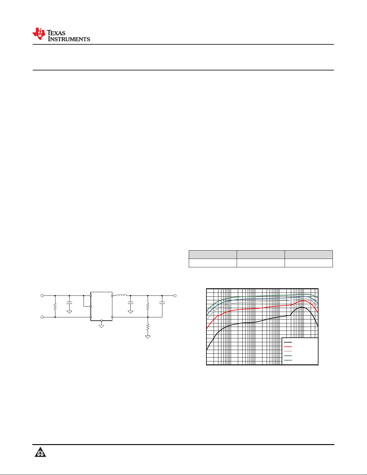
R1
200 k
R2
100 k
SW
GND FB
EN
PG
VIN
C2
3x10 µF
R3
100 k
C1
4.7 µF
V
IN
2.5 V to 5.5 V
V
PG
V
OUT
1.8 V
L1
0.47 µH
TLV62595
C3
120 pF
Load (A)
Efficiency (%)
50
55
60
65
70
75
80
85
90
95
100
100P 1m 10m 100m 1 4
D007
V
OUT
= 0.6V
V
OUT
= 1.2V
V
OUT
= 1.8V
V
OUT
= 2.5V
V
OUT
= 3.3V
TLV62595
www.ti.com
SLUSDR2 – DECEMBER 2020
SLUSDR2 – DECEMBER 2020
TLV62595
TLV62595, 2.5-V to 5.5-V Input, 4-A Step-Down Converter with 1% Output Accuracy in
1.5-mm × 1.5-mm QFN Package
1 Features
• Up to 97% efficiency
• Low R
power switches 26 mΩ / 25 mΩ
DS(ON)
• 2.5-V to 5.5-V input voltage range
• Adjustable output voltage from 0.6 V to 4 V
• 1% feedback voltage accuracy (full temperature
range)
• DCS-control topology
• Power save mode for light load efficiency
• 100% duty cycle for lowest dropout
• 10-μA operating quiescent current
• 2.2-MHz typical switching frequency
• Short circuit protection (HICCUP)
• Active output discharge
• Power good output
• Thermal shutdown protection
• Create a custom design using the TLV62595 with
the WEBENCH® Power Designer
2 Applications
• Solid state drive
• Portable electronics
• IP network camera
• Industrial PC
• Multifunction printers
3 Description
The TLV62595 is a high-frequency synchronous stepdown converter optimized for compact solution size
and high efficiency. The device integrates switches
capable of delivering an output current up to 4 A. At
medium to heavy loads, the converter operates in
pulse width modulation (PWM) mode with typical 2.2MHz switching frequency. At light load, the device
automatically enters Power Save Mode (PSM) to
maintain high efficiency over the entire load current
range with a quiescent current as low as 10-µA.
Based on the DCS Control topology, it provides a fast
transient response. The internal reference regulates
the output voltage down to 0.6 V with a high feedback
voltage accuracy of 1% over the junction temperature
range of –40°C to 125°C. The entire solution requires
a small 470-nH inductor, a single 4.7-μF input
capacitor and three 10-μF or single 47-μF output
capacitor.
The device is available in a 6-pin 1.5-mm x 1.5-mm
QFN package, offering a high power density solution.
Device Information
PART NUMBER PACKAGE
TLV62595 6-Pin VSON-HR 1.5 mm x 1.5 mm
(1) For all available packages, see the orderable addendum at
the end of the data sheet.
(1)
BODY SIZE (NOM)
Typical Application Schematic
Copyright © 2020 Texas Instruments Incorporated
An IMPORTANT NOTICE at the end of this data sheet addresses availability, warranty, changes, use in safety-critical applications,
intellectual property matters and other important disclaimers. PRODUCTION DATA.
Efficiency at VIN = 5 V
Product Folder Links: TLV62595
Submit Document Feedback
1
TLV62595
SLUSDR2 – DECEMBER 2020
www.ti.com
Table of Contents
1 Features............................................................................1
2 Applications.....................................................................1
3 Description.......................................................................1
4 Revision History.............................................................. 2
5 Pin Configuration and Functions...................................3
6 Specifications.................................................................. 4
6.1 Absolute Maximum Ratings........................................ 4
6.2 ESD Ratings............................................................... 4
6.3 Recommended Operating Conditions.........................4
6.4 Thermal Information....................................................4
6.5 Electrical Characteristics.............................................5
6.6 Typical Characteristics................................................6
7 Detailed Description........................................................7
7.1 Overview.....................................................................7
7.2 Functional Block Diagram...........................................7
7.3 Feature Description.....................................................8
7.4 Device Functional Modes............................................9
4 Revision History
DATE REVISION NOTES
December 2020 * Initial release
8 Application and Implementation..................................10
8.1 Application Information............................................. 10
8.2 Typical Application....................................................10
9 Power Supply Recommendations................................18
10 Layout...........................................................................19
10.1 Layout Guidelines................................................... 19
10.2 Layout Example...................................................... 19
11 Device and Documentation Support..........................20
11.1 Device Support........................................................20
11.2 Documentation Support.......................................... 20
11.3 Receiving Notification of Documentation Updates..20
11.4 Support Resources................................................. 20
11.5 Trademarks............................................................. 20
11.6 Electrostatic Discharge Caution..............................21
11.7 Glossary..................................................................21
12 Mechanical, Packaging, and Orderable
Information.................................................................... 21
2 Submit Document Feedback
Copyright © 2020 Texas Instruments Incorporated
Product Folder Links: TLV62595
SW
VIN
GND
PG
EN
FB
1
2
3
6
5
4
www.ti.com
5 Pin Configuration and Functions
Figure 5-1. 6-Pin VSON-HR DMQ Package (Bottom View)
Table 5-1. Pin Functions
PIN
NAME NO.
EN 1 I
PG 2 O
FB 3 I
GND 4 Ground pin
SW 5 PWR Switch pin of the power stage
VIN 6 PWR Input voltage pin
I/O DESCRIPTION
Device enable pin. To enable the device, this pin needs to be pulled high. Pulling this pin low
disables the device. Do not leave floating.
Power-good open-drain output pin. The pullup resistor can be connected to voltages up to
5.5 V. If unused, leave it floating.
Feedback pin. For the fixed output voltage versions, this pin must be connected to the
output.
SLUSDR2 – DECEMBER 2020
TLV62595
Copyright © 2020 Texas Instruments Incorporated
Product Folder Links: TLV62595
Submit Document Feedback
3
TLV62595
SLUSDR2 – DECEMBER 2020
www.ti.com
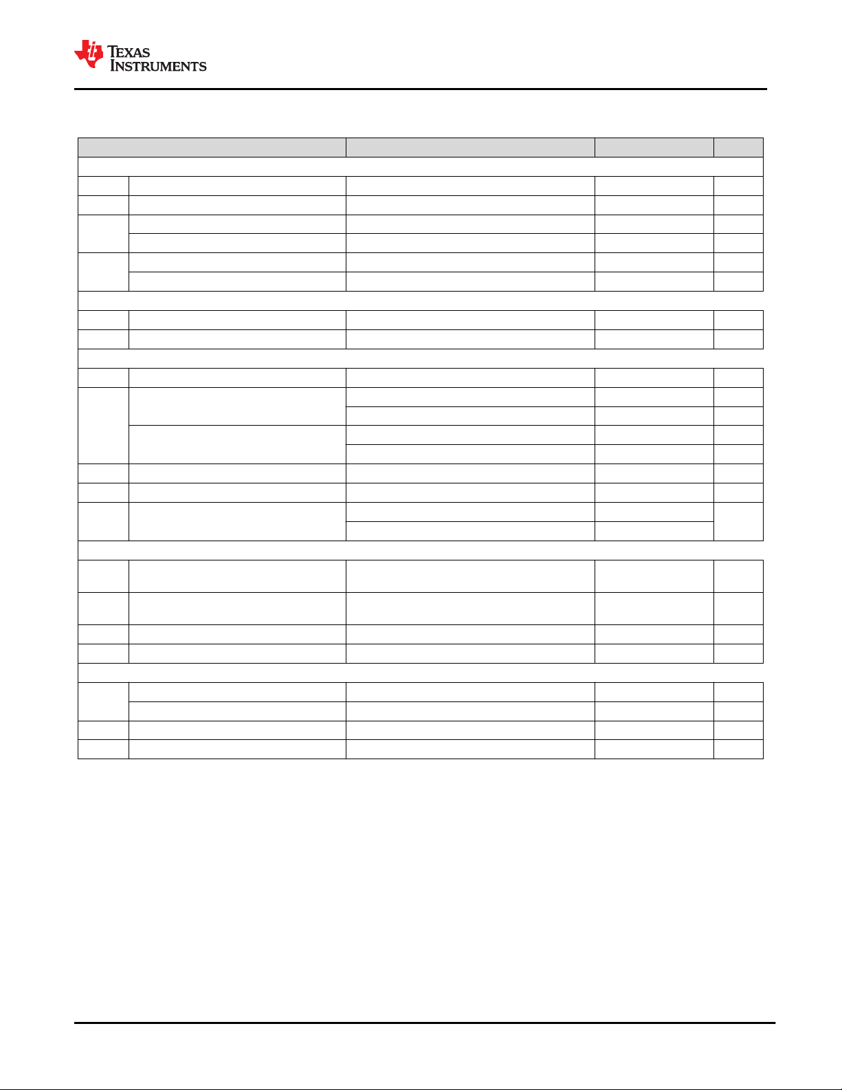
6 Specifications
6.1 Absolute Maximum Ratings
over operating temperature range (unless otherwise noted)
Pin voltage
Pin voltage
Pin voltage
Pin voltage
Temperature Operating Junction, T
Temperature Storage, T
(1) Stresses beyond those listed under Absolute Maximum Rating may cause permanent damage to the device. These are stress ratings
(2) All voltage values are with respect to the network ground terminal
(3) While switching
(2)
(2)
(2)
(2)
VIN, FB, EN, PG – 0.3 6 V
SW (DC) – 0.3 VIN + 0.3 V
SW (DC, in current limit) – 1 VIN + 0.3
SW (AC, less than 10ns)
STG
(3)
J
only, which do not imply functional operation of the device at these or any other conditions beyond those indicated under
Recommended Operating Condition. Exposure to absolute-maximum-rated conditions for extended periods may affect device
reliability.
6.2 ESD Ratings
Human body model (HBM), per ANSI/ESDA/JEDEC
(1)
V
(ESD)
Electrostatic discharge
JS-001
Charged device model (CDM), per JEDEC
specificationJESD22-C101
(1)
MIN MAX UNIT
– 2.5 10 V
–40 150 °C
–65 150 °C
VALUE UNIT
±2000
V
(2)
±500
(1) JEDEC document JEP155 states that 500-V HBM allows safe manufacturing with a standard ESD control process.
(2) JEDEC document JEP157 states that 250-V CDM allows safe manufacturing with a standard ESD control process.
6.3 Recommended Operating Conditions
Over operating temperature range (unless otherwise noted)
MIN NOM MAX UNIT
V
IN
V
OUT
I
OUT
V
PG
I
SINK_PG
T
J
Input voltage range 2.5 5.5 V
Output voltage range 0.6 4.0 V
Output curent range 0 4 A
Pull-up resistor voltage 5.5 V
Sink current at PG pin 1 mA
Operating junction temperature –40 125 °C
6.4 Thermal Information
TLV62595 TLV62595EVM-794
(1)
6 PINS 6 PINS
R
θJA
R
θJC(top)
R
θJB
Ψ
JT
Y
JB
THERMAL METRIC
Junction-to-ambient thermal resistance 129.5 71.4 °C/W
Junction-to-case (top) thermal resistance 103.9 n/a °C/W
Junction-to-board thermal resistance 33.1 n/a °C/W
Junction-to-top characterization parameter 3.8 3.9 °C/W
Junction-to-board characterization parameter 33.1 38.6 °C/W
UNITDMQ (JEDEC) DMQ (EVM)
(1) For more information about traditional and new thermal metrics, see the Semiconductor and IC Package Thermal Metrics application
report.
4 Submit Document Feedback
Copyright © 2020 Texas Instruments Incorporated
Product Folder Links: TLV62595
www.ti.com
6.5 Electrical Characteristics
TJ = 25 °C and VIN = 5 V, unless otherwise noted.
PARAMETER TEST CONDITIONS MIN TYP MAX UNIT
SUPPLY
I
Q
I
SD
V
UVLO
T
JSD
LOGIC INTERFACE EN
V
IH
V
IL
SOFT START, POWER GOOD
t
SS
V
PG
V
PG,OL
I
PG,LKG
t
PG,DLY
OUTPUT
V
FB
I
FB,LKG
I
DIS
POWER SWITCH
R
DS(on)
I
LIM
f
SW
Quiescent current EN = High, no load, device not switching 10 µA
Shutdown current EN = Low, TJ = -40℃ to 85℃ 0.05 µA
Undervoltage lock out threshold VIN falling 2.1 2.2 2.3 V
Undervoltage lock out hysteresis VIN rising 160 mV
Thermal shutdown threshold TJ rising 150 °C
Thermal shutdown hysteresis TJ falling 20 °C
High-level threshold voltage VIN = 2.5 V to 5.5 V 1.0 V
Low-level threshold voltage VIN = 2.5 V to 5.5 V 0.4 V
Soft start time Time from EN high to 95% of V
Power good lower threshold
Power good upper threshold
Low-level output voltage I
Input leakage current into PG pin VPG = 5.0 V 0.01 µA
Power good deglitch delay
Feedback regulation voltage
Feedback input leakage current for
adjustable output voltage
Output discharge current VSW = 0.4V; EN = LOW 400 mA
Load regulation I
High-side FET on-resistance 26 mΩ
Low-side FET on-resistance 25 mΩ
High-side FET switch current limit, DC 4.8 5.6 A
PWM switching frequency I
SLUSDR2 – DECEMBER 2020
TLV62595
nominal 1.75 ms
OUT
VPG rising, VFB referenced to VFB nominal 96 %
VPG falling, VFB referenced to VFB nominal 92 %
VPG rising, VFB referenced to VFB nominal 105 %
VPG falling, VFB referenced to VFB nominal 110 %
= 1 mA 0.4 V
sink
PG rising edge 100
PG falling edge 20
PWM mode, 2.5 V ≤ VIN ≤ 5.5 V, TJ = -40°C to
125°C
594 600 606 mV
VFB = 0.6 V 0.01 µA
= 0.5 A to 3 A, V
OUT
= 1 A, V
OUT
OUT
= 1.8 V 0.1 %/A
OUT
= 1.8 V 2.2 MHz
µs
Copyright © 2020 Texas Instruments Incorporated
Product Folder Links: TLV62595
Submit Document Feedback
5
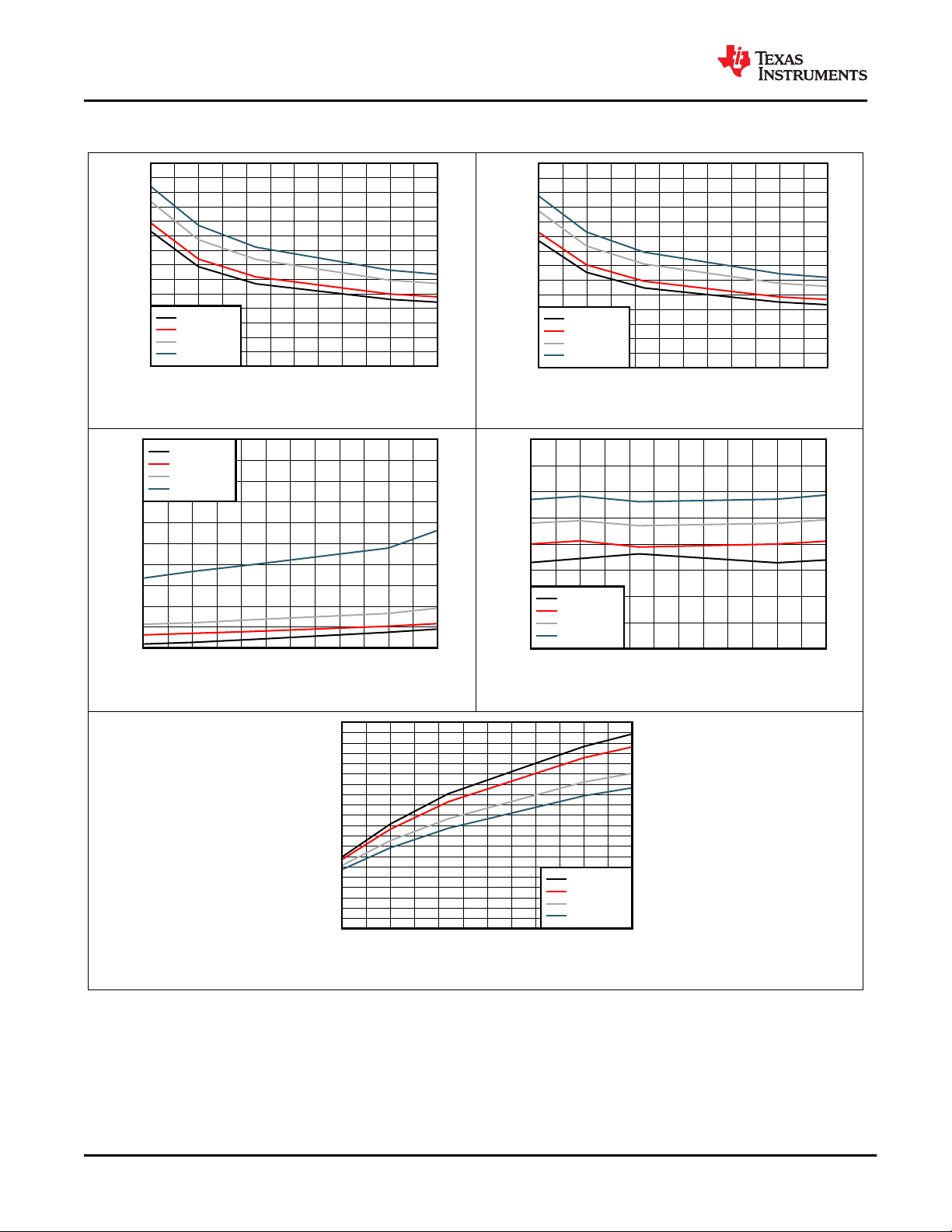
Input Voltage (V)
R
DS(on)
(mOhm)
2.5 3.0 3.5 4.0 4.5 5.0 5.5
0.0
10.0
20.0
30.0
40.0
50.0
60.0
70.0
D010
TJ = 0 °C
TJ = 25 °C
TJ = 85 °C
TJ = 125 °C
Input Voltage (V)
R
DS(on)
(mOhm)
2.5 3.0 3.5 4.0 4.5 5.0 5.5
0.0
10.0
20.0
30.0
40.0
50.0
60.0
70.0
D011
TJ = 0 °C
TJ = 25 °C
TJ = 85 °C
TJ = 125 °C
Input Voltage (V)
6KXWGRZQ&XUUHQW$
2.5 3.0 3.5 4.0 4.5 5.0 5.5
0.0
0.1
0.2
0.3
0.4
0.5
D000
TJ = -40 °C
TJ = 25 °C
TJ = 85 °C
TJ = 125 °C
Input Voltage (V)
4XLHVFHQW&XUUHQW$
2.5 3.0 3.5 4.0 4.5 5.0 5.5
0.0
2.0
4.0
6.0
8.0
D001
TJ = -40 °C
TJ = 25 °C
TJ = 85 °C
TJ = 125 °C
Input Voltage (V)
Output Discharge Current (mA)
2.5 3.0 3.5 4.0 4.5 5.0 5.5
0
50
100
150
200
250
300
350
400
450
500
D012
TJ = 0 °C
TJ = 25 °C
TJ = 85 °C
TJ = 125 °C
TLV62595
SLUSDR2 – DECEMBER 2020
6.6 Typical Characteristics
www.ti.com
Figure 6-1. High-Side FET On-Resistance
Figure 6-3. Shutdown Current
Figure 6-2. Low-Side FET On-Resistance
Figure 6-4. Quiescent Current
6 Submit Document Feedback
Figure 6-5. Output Discharge Current
Product Folder Links: TLV62595
Copyright © 2020 Texas Instruments Incorporated
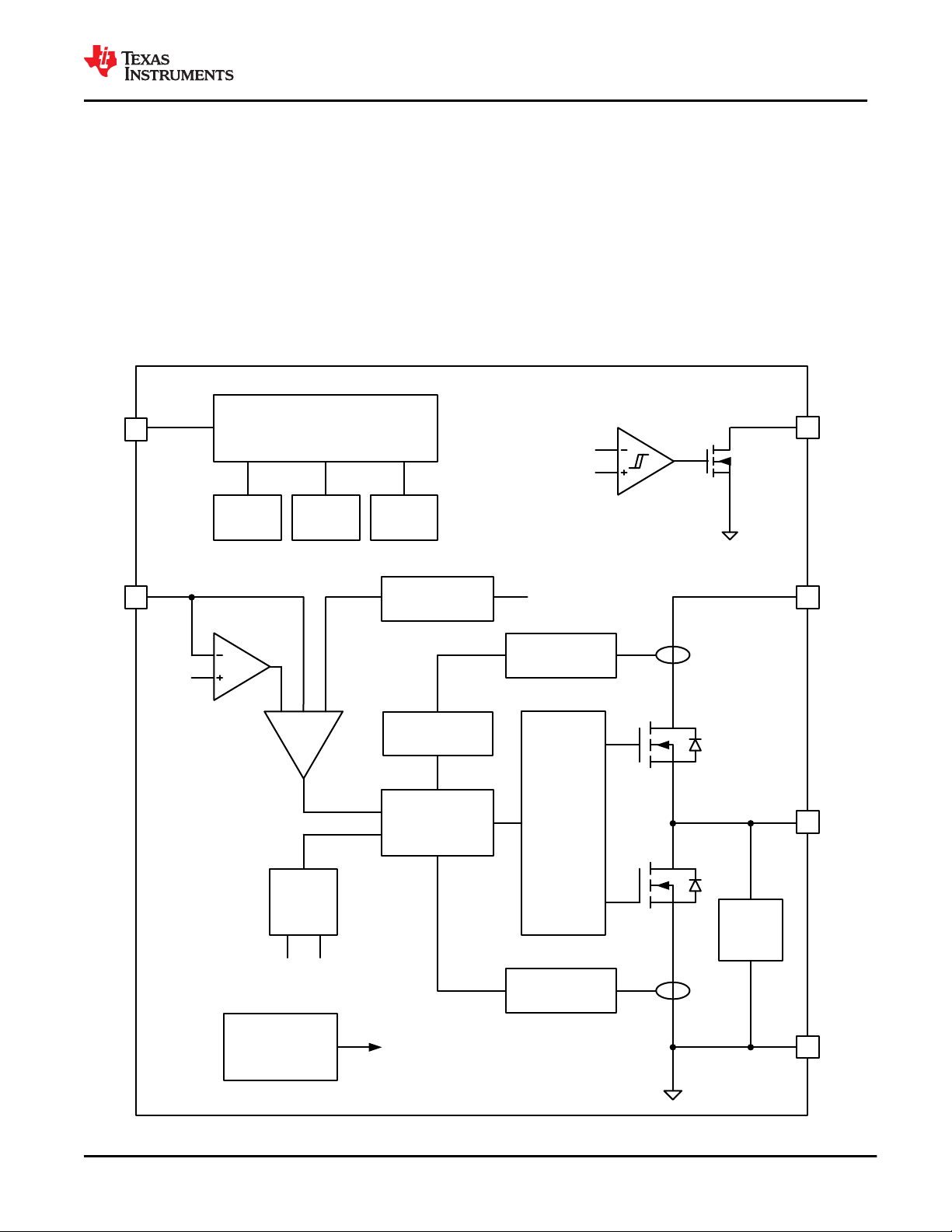
UVLO
Control Logic
Soft-Start
Thermal
Shutdown
Gate Drive
Peak Current Detect
Zero Current Detect
HICCUP
Modulator
Ton
Ramp
EA
V
SW
V
SW
V
REF
V
FB
V
REF
V
IN
V
SW
V
FB
V
REF
Comp
V
IN
FB
EN
0.6 V
Or
Fixed Output Voltages
PG
VIN
SW
GND
Output
Discharge
www.ti.com
SLUSDR2 – DECEMBER 2020
7 Detailed Description
7.1 Overview
The TLV62595 are synchronous step-down converters based on the DCS-Control topology with an adaptive
constant on-time control and a stabilized switching frequency. It operates in PWM (pulse width modulation) mode
for medium to heavy loads and in PSM (power save mode) at light load conditions, keeping the output voltage
ripple small. The nominal switching frequency is about 2.2 MHz with a small and controlled variation over the
input voltage range. As the load current decreases, the converter enters PSM, reducing the switching frequency
to keep efficiency high over the entire load current range. Since combining both PWM and PSM within a single
building block, the transition between modes is seamless and without effect on the output voltage. The devices
offer both excellent dc voltage and fast load transient regulation, combined with a very low output voltage ripple.
7.2 Functional Block Diagram
TLV62595
Copyright © 2020 Texas Instruments Incorporated
Product Folder Links: TLV62595
Submit Document Feedback
7

ns
V
V
OUT
ON
450×=
×
=
-
é ù
×
ê ú
ë û
2
2
OUT
PSM
IN OUT
IN
ON
OUT
I
f
V V
V
T
V L
IN,MIN OUT OUT,MAX DS(on) L
V V I (R + R )= + ´
TLV62595
SLUSDR2 – DECEMBER 2020
www.ti.com
7.3 Feature Description
7.3.1 Pulse Width Modulation (PWM) Operation
At load currents larger than half the inductor ripple current, the device operates in pulse width modulation in
continuous conduction mode (CCM). The PWM operation is based on an adaptive constant on-time control with
stabilized switching frequency. To achieve a stable switching frequency in a steady state condition, the on-time is
calculated as:
(1)
7.3.2 Power Save Mode (PSM) Operation
To maintain high efficiency at light loads, the device enters power save mode (PSM) at the boundary to
discontinuous conduction mode (DCM). This happens when the output current becomes smaller than half of the
ripple current of the inductor. The device operates now with a fixed on-time and the switching frequency further
decreases proportionally to the load current. It can be calculated as:
(2)
In PSM, the output voltage rises slightly above the nominal target, which can be minimized using larger output
capacitance. At duty cycles larger than 90%, the device may not enter PSM. The device maintains output
regulation in PWM mode.
7.3.3 Minimum Duty Cycle and 100% Mode Operation
There is no limitation for small duty cycles, since even at very low duty cycles, the switching frequency is
reduced as needed to always ensure a proper regulation.
If the output voltage level comes close to the input voltage, the device enters 100% mode. While the high-side
switch is constantly turned on, the low-side switch is switched off. The difference between VIN and VOUT is
determined by the voltage drop across the high-side FET and the dc resistance of the inductor. The minimum
VIN that is needed to maintain a specific VOUT value is estimated as:
(3)
where
• V
• I
• R
= Minimum input voltage to maintain an output voltage
IN,MIN
OUT,MAX
= Maximum output current
= High-side FET ON-resistance
DS(on)
• RL = Inductor ohmic resistance (DCR)
7.3.4 Soft Start
About 250 μs after EN goes high, the internal soft-start circuitry controls the output voltage during start-up. This
avoids excessive inrush current and ensures a controlled output voltage ramp. It also prevents unwanted voltage
drops from high-impedance power sources or batteries. The TLV62595 can start into a pre-biased output.
7.3.5 Switch Current Limit and HICCUP Short-Circuit Protection
The switch current limit prevents the device from drawing excessive current in case of externally-caused
overcurrent or short circuit condition. Due to an internal propagation delay (typically 60 ns), the actual ac peak
current can exceed the static current limit during that time.
8 Submit Document Feedback
Copyright © 2020 Texas Instruments Incorporated
Product Folder Links: TLV62595
www.ti.com
SLUSDR2 – DECEMBER 2020
TLV62595
If the current limit threshold is reached, the device delivers its maximum output current. Detecting this condition
for 32 switching cycles (about 13 μs), the device turns off the high-side MOSFET for about 100 μs which allows
the inductor current to decrease through the low-side MOSFET's body diode and then restart again with a soft
start cycle. As long as the overload condition is present, the device hiccups that way, limiting the output power.
7.3.6 Undervoltage Lockout
The undervoltage lockout (UVLO) function prevents misoperation of the device, if the input voltage drops below
the UVLO threshold. It is set to about 2.2 V with a hysteresis of typically 160 mV.
7.3.7 Thermal Shutdown
The junction temperature (TJ) of the device is monitored by an internal temperature sensor. If TJ exceeds 150°C
(typ.), the device goes in thermal shutdown with a hysteresis of typically 20°C. Once the TJ has decreased
enough, the device resumes normal operation.
7.4 Device Functional Modes
7.4.1 Enable, Disable and Output Discharge
The device starts operation, when Enable (EN) is set High. The input threshold levels are typically 0.9 V for
rising and 0.7 V for falling signals. Do not leave EN floating. Shutdown is forced if EN is pulled low with a
shutdown current of typically 50 nA. During shutdown, the internal power MOSFETs as well as the entire control
circuitry, are turned off and the output voltage is actively discharged through the SW pin by a current sink.
Therefore VIN must remain present for the discharge to function.
7.4.2 Power Good
The TLV62595 has a built-in power good (PG) function. The PG pin goes high impedance, when the output
voltage has reached its nominal value. Otherwise, including when disabled, in UVLO or in thermal shutdown, PG
is low (see Table 7-1). The PG function is formed with a window comparator, which has an upper and lower
voltage threshold. The PG pin is an open-drain output and is specified to sink up to 1 mA. The power good
output requires a pullup resistor connecting to any voltage rail less than 5.5 V.
The PG signal can be used for sequencing of multiple rails by connecting it to the EN pin of other converters.
Leave the PG pin unconnected when not used. The PG rising edge has a 100-µs blanking time and the PG
falling edge has a deglitch delay of 20 µs.
Table 7-1. PG Pin Logic
DEVICE CONDITIONS
EN = High, VFB ≥ 0.576 V √
Enable
Shutdown EN = Low √
Thermal Shutdown TJ > T
UVLO 0.7 V < VIN < V
Power Supply Removal VIN < 0.7 V √
EN = High, VFB ≤ 0.552 V √
EN = High, VFB ≤ 0.63 V √
EN = High, VFB ≥ 0.66 V √
JSD
UVLO
HIGH Z LOW
LOGIC STATUS
√
√
Copyright © 2020 Texas Instruments Incorporated
Product Folder Links: TLV62595
Submit Document Feedback
9

R1
200 k
R2
100 k
SW
GND FB
EN
PG
VIN
C2
3x10 µF
R3
100 k
C1
4.7 µF
V
IN
2.5 V to 5.5 V
V
PG
V
OUT
1.8 V
L1
0.47 µH
TLV62595
C3
120 pF
TLV62595
SLUSDR2 – DECEMBER 2020
www.ti.com
8 Application and Implementation
Note
Information in the following applications sections is not part of the TI component specification, and TI
does not warrant its accuracy or completeness. TI’s customers are responsible for determining
suitability of components for their purposes, as well as validating and testing their design
implementation to confirm system functionality.
8.1 Application Information
The following section discusses the design of the external components to complete the power supply design for
several input and output voltage options by using typical applications as a reference.
8.2 Typical Application
Figure 8-1. Typical Application of TLV62595
8.2.1 Design Requirements
For this design example, use the parameters listed in Table 8-1 as the input parameters.
Table 8-1. Design Parameters
DESIGN PARAMETER EXAMPLE VALUE
Input voltage, TLV62595 2.5 V to 5.5 V
Output voltage 1.8 V
Output ripple voltage <20 mV
Maximum output current, TLV62595 4 A
Table 8-2 lists the components used for the example.
Table 8-2. List of Components
REFERENCE DESCRIPTION MANUFACTURER
C1 4.7 µF, Ceramic capacitor, 6.3 V, X7R, size 0603, JMK107BB7475MA Taiyo Yuden
C2 3 x 10 µF, Ceramic capacitor, 10 V, X7R, size 0603, GRM188Z71A106MA73D Murata
C3 120 pF, Ceramic capacitor, 50 V, size 0402 Std
L1 0.47 µH, Power Inductor, XFL4015-471MEB Coilcraft
R1 Depending on the output voltage, 1%, size 0402 Std
R2 100 kΩ, Chip resistor, 1/16 W, 1%, size 0402 Std
R3 100 kΩ, Chip resistor, 1/16 W, 1%, size 0402 Std
1. See the Third-Party Products Disclaimer.
10 Submit Document Feedback
Product Folder Links: TLV62595
Copyright © 2020 Texas Instruments Incorporated

OUT OUT
FB
V V
R1 R2 1 R2 1
V 0.6V
§ ·
§ ·
u u
¨ ¸
¨ ¸
© ¹
© ¹
µ12
3C
www.ti.com
SLUSDR2 – DECEMBER 2020
8.2.2 Detailed Design Procedure
8.2.2.1 Custom Design With WEBENCH® Tools
Click here to create a custom design using the TLV62595 device with the WEBENCH® Power Designer.
TLV62595
1. Start by entering the input voltage (VIN), output voltage (V
), and output current (I
OUT
) requirements.
OUT
2. Optimize the design for key parameters such as efficiency, footprint, and cost using the optimizer dial.
3. Compare the generated design with other possible solutions from Texas Instruments.
The WEBENCH Power Designer provides a customized schematic along with a list of materials with real-time
pricing and component availability.
In most cases, these actions are available:
• Run electrical simulations to see important waveforms and circuit performance
• Run thermal simulations to understand board thermal performance
• Export customized schematic and layout into popular CAD formats
• Print PDF reports for the design, and share the design with colleagues
Get more information about WEBENCH tools at www.ti.com/WEBENCH.
8.2.2.2 Setting The Output Voltage
The output voltage is set by an external resistor divider according to Equation 4:
(4)
R2 must not be higher than 100 kΩ to achieve high efficiency at light load while providing acceptable noise
sensitivity. Equation 5 shows how to compute the value of the feedforward capacitor for a given R2 value. For
the recommended 100 k value for R2, a 120-pF feedforward capacitor is used.
(5)
For the fixed output voltage versions, connect the FB pin to the output. R1, R2, and C3 are not needed. The
fixed output voltage devices have an internal feedforward capacitor.
8.2.2.3 Output Filter Design
The inductor and the output capacitor together provide a low-pass filter. To simplify this process, Table 8-3
outlines possible inductor and capacitor value combinations for most applications. Checked cells represent
combinations that are proven for stability by simulation and lab test. Further combinations should be checked for
each individual application.
Table 8-3. Matrix of Output Capacitor and Inductor Combinations, TLV62595
NOMINAL L [µH]
0.33
0.47 + +
1.0
(1) This LC combination is the standard value and recommended for most applications.
(2) Inductor tolerance and current derating is anticipated. The effective inductance can vary by 20% and –30%.
(3) Capacitance tolerance and bias voltage derating is anticipated. The effective capacitance can vary by 20% and –35%.
(2)
10 2 x 10 or 22 47 100
NOMINAL C
(1)
OUT
[µF]
(3)
+
Copyright © 2020 Texas Instruments Incorporated
Product Folder Links: TLV62595
Submit Document Feedback
11

SW
IN
OUT
OUTL
L
MAX,OUTMAX,L
fL
V
V
1
VI
2
I
II
´
-
´=D
D
+=
TLV62595
SLUSDR2 – DECEMBER 2020
www.ti.com
Table 8-4. Matrix of Output Capacitor and Inductor Combinations, TLV62595
NOMINAL L [µH]
0.33
0.47 +
1.0
(2)
22 3 x 10 47 100
NOMINAL C
(1)
OUT
(3)
[µF]
+ +
8.2.2.4 Inductor Selection
The main parameter for the inductor selection is the inductor value and then the saturation current of the
inductor. To calculate the maximum inductor current under static load conditions, Equation 6 is given.
(6)
where
• I
OUT,MAX
= Maximum output current
• ΔIL = Inductor current ripple
• fSW = Switching frequency
• L = Inductor value
It is recommended to choose a saturation current for the inductor that is approximately 20% to 30% higher than
I
. In addition, DC resistance and size should also be taken into account when selecting an appropriate
L,MAX
inductor. Table 8-5 lists recommended inductors.
Table 8-5. List of Recommended Inductors
INDUCTANCE
[µH]
0.47
(1) See Third-party Products Disclaimer.
CURRENT RATING
[A]
4.8 2.0 x 1.6 x 1.0 32 HTEN20161T-R47MDR, Cyntec
4.6 2.0 x 1.2 x 1.0 25 HTEH20121T-R47MSR, Cyntec
4.8 2.0 x 1.6 x 1.0 32 DFE201610E - R47M, MuRata
4.8 2.0 x 1.6 x 1.0 32 DFE201210S - R47M, MuRata
5.1 2.0 x 1.6 x 1.0 34 TFM201610ALM-R47MTAA, TDK
5.2 2.0 x 1.6 x 1.0 25 TFM201610ALC-R47MTAA, TDK
6.6 4.0 x 4.0 x 1.6 8.36 XFL4015-471ME, Coilcraft
8.0 3.5 x 3.2 x 2.0 10.85 XEL3520-471ME, Coilcraft
6.8 4.5 x 4 x 1.8 11.2 WE-LHMI-744373240047, Würth
DIMENSIONS [L x W x
H mm]
MAX. DC
RESISTANCE [mΩ]
MFR PART NUMBER
(1)
8.2.2.5 Capacitor Selection
The input capacitor is the low-impedance energy source for the converters which helps to provide stable
operation. A low-ESR multilayer ceramic capacitor is recommended for best filtering and must be placed
between VIN and GND as close as possible to those pins. For most applications, a minimum effective input
capacitance of 3 µF should be present, though a larger value reduces input current ripple.
The architecture of the device allows the use of tiny ceramic output capacitors with low equivalent series
resistance (ESR). These capacitors provide low output voltage ripple and are recommended. To keep its low
resistance up to high frequencies and to get narrow capacitance variation with temperature, TI recommends
12 Submit Document Feedback
Product Folder Links: TLV62595
Copyright © 2020 Texas Instruments Incorporated

www.ti.com
SLUSDR2 – DECEMBER 2020
using X7R or X5R dielectrics. Considering the DC-bias derating the capacitance, the minimum effective output
capacitance is 20 µF for TLV62595.
A feedforward capacitor is required for the adjustable version, as described in Section 8.2.2.2. This capacitor is
not required for the fixed output voltage versions.
TLV62595
Copyright © 2020 Texas Instruments Incorporated
Product Folder Links: TLV62595
Submit Document Feedback
13

Load (A)
Efficiency (%)
45
50
55
60
65
70
75
80
85
90
95
100P 1m 10m 100m 1 4
D002
VIN = 2.5V
VIN = 3.3V
VIN = 4.2V
VIN = 5.0V
Load (A)
Vout (V)
0.588
0.591
0.594
0.597
0.6
0.603
0.606
0.609
0.612
100P 1m 10m 100m 1 4
D021
VIN = 2.5 V
VIN = 3.3 V
VIN = 4.2 V
VIN = 5.0 V
Load (A)
Efficiency (%)
55
60
65
70
75
80
85
90
95
100
100P 1m 10m 100m 1 4
D003
VIN = 2.5V
VIN = 3.3V
VIN = 4.2V
VIN = 5.0V
Load (A)
Vout (V)
1.188
1.191
1.194
1.197
1.2
1.203
1.206
1.209
1.212
100P 1m 10m 100m 1 4
D031
VIN = 2.4 V
VIN = 3.3 V
VIN = 4.5 V
VIN = 5.0 V
Load (A)
Efficiency (%)
60
65
70
75
80
85
90
95
100
100P 1m 10m 100m 1 4
D004
VIN = 2.5V
VIN = 3.3V
VIN = 4.2V
VIN = 5.0V
Load (A)
Vout (V)
1.782
1.788
1.794
1.8
1.806
1.812
1.818
100P 1m 10m 100m 1 4
D041
VIN = 2.5 V
VIN = 3.3 V
VIN = 4.2 V
VIN = 5.0 V
TLV62595
SLUSDR2 – DECEMBER 2020
8.2.3 Application Curves
www.ti.com
VIN = 5.0 V, V
= 1.8 V, TA = 25°C, BOM = Table 8-2, unless otherwise noted.
OUT
V
= 0.6 V
OUT
Figure 8-2. Efficiency
V
= 0.6 V
OUT
Figure 8-3. Load Regulation
V
= 1.2 V
OUT
Figure 8-4. Efficiency
14 Submit Document Feedback
Figure 8-6. Efficiency
V
OUT
= 1.8 V
Product Folder Links: TLV62595
V
= 1.2 V
OUT
Figure 8-5. Load Regulation
V
= 1.8 V
OUT
Figure 8-7. Load Regulation
Copyright © 2020 Texas Instruments Incorporated

Load (A)
Efficiency (%)
60
65
70
75
80
85
90
95
100
100P 1m 10m 100m 1 4
D006
VIN = 3.3V
VIN = 4.2V
VIN = 5.0V
Load (A)
Vout (V)
2.475
2.485
2.495
2.505
2.515
2.525
100P 1m 10m 100m 1 4
D061
VIN = 3.3 V
VIN = 4.2 V
VIN = 5.0 V
Load (A)
Efficiency (%)
70
75
80
85
90
95
100
100P 1m 10m 100m 1 4
D005
VIN = 4.2V
VIN = 5.0V
Load (A)
Vout (V)
3.260
3.280
3.300
3.320
3.340
100P 1m 10m 100m 1 4
D051
VIN = 4.2V
VIN = 5.0V
Load (A)
Switching Frequency (kHz)
0.0 0.5 1.0 1.5 2.0 2.5 3.0 3.5 4.0
0
250
500
750
1000
1250
1500
1750
2000
2250
2500
2750
3000
D013
V
OUT
= 0.6V
V
OUT
= 1.2V
V
OUT
= 1.8V
V
OUT
= 2.5V
Input Voltage (V)
Switching Frequency (kHz)
2.5 3.0 3.5 4.0 4.5 5.0 5.5
0
250
500
750
1000
1250
1500
1750
2000
2250
2500
2750
3000
D014
V
OUT
= 0.6V
V
OUT
= 1.2V
V
OUT
= 1.8V
V
OUT
= 2.5V
V
OUT
= 3.3V
www.ti.com
V
OUT
= 2.5 V
V
OUT
SLUSDR2 – DECEMBER 2020
TLV62595
= 2.5 V
Figure 8-8. Efficiency
V
= 3.3 V
OUT
Figure 8-10. Efficiency
Figure 8-9. Load Regulation
V
= 3.3 V
OUT
Figure 8-11. Load Regulation
VIN = 3.3 V
Copyright © 2020 Texas Instruments Incorporated
Figure 8-12. Switching Frequency
Figure 8-13. Switching Frequency
Product Folder Links: TLV62595
I
OUT
= 1.0 A
Submit Document Feedback
15

Ambient Temperature (°C)
Output Current (A)
45 55 65 75 85 95 105 115 125
0
1
2
3
4
5
D020
VIN = 2.5 V
VIN = 3.3 V
VIN = 5.0 V
Ambient Temperature (°C)
Output Current (A)
45 55 65 75 85 95 105 115 125
0
1
2
3
4
5
D015
VIN = 2.5 V
VIN = 3.3 V
VIN = 5.0 V
Ambient Temperature (°C)
Output Current (A)
45 55 65 75 85 95 105 115 125
0
1
2
3
4
5
D017
VIN = 3.3 V
VIN = 5.0 V
Ambient Temperature (°C)
Output Current (A)
45 55 65 75 85 95 105 115 125
0
1
2
3
4
5
D016
VIN = 5.0 V
TLV62595
SLUSDR2 – DECEMBER 2020
V
= 1.2 V θJA= 71.4 °C/W
OUT
V
= 1.8 V θJA= 71.4 °C/W
OUT
www.ti.com
Figure 8-14. Thermal Derating
V
= 2.5 V θJA= 71.4 °C/W
OUT
Figure 8-16. Thermal Derating
Figure 8-15. Thermal Derating
V
= 3.3 V θJA= 71.4 °C/W
OUT
Figure 8-17. Thermal Derating
I
= 1.0 A
16 Submit Document Feedback
Figure 8-18. PWM Operation
OUT
Product Folder Links: TLV62595
I
= 0.1 A
OUT
Figure 8-19. PSM Operation
Copyright © 2020 Texas Instruments Incorporated

www.ti.com
SLUSDR2 – DECEMBER 2020
TLV62595
Load = 0.6 Ω
Figure 8-20. Start-up with Load
Load = 1.8 Ω
Figure 8-22. Disable, Active Output Discharge
Figure 8-21. Startup with No Load
Figure 8-23. Disable, Active Output Discharge at
No Load
I
= 0.05 A to 1A
OUT
Figure 8-24. Load Transient
Copyright © 2020 Texas Instruments Incorporated
Product Folder Links: TLV62595
I
= 1 A to 2 A
OUT
Figure 8-25. Load Transient
Submit Document Feedback
17

7LPHV',9
D018
V
OUT
1V/DIV
I
COIL
2A/DIV
V
PG
5V/DIV
7LPHV',9
D019
V
OUT
1V/DIV
I
COIL
2A/DIV
V
PG
5V/DIV
TLV62595
SLUSDR2 – DECEMBER 2020
I
OUT
= 1 A
I
OUT
www.ti.com
= 1 A
Figure 8-26. HICCUP Short Circuit Protection
Figure 8-27. HICCUP Short Circuit Protection
(Zoom In)
9 Power Supply Recommendations
The device is designed to operate from an input voltage supply range from 2.4 V to 5.5 V. Ensure that the input
power supply has a sufficient current rating for the application.
18 Submit Document Feedback
Copyright © 2020 Texas Instruments Incorporated
Product Folder Links: TLV62595

L1
VIN
GND
VOUT
C2
C1
C3
R1
R2
L1
C1
G
N
D
E
N
P
G
F
B
S
W
V
I
N
Solution size = 31mm
2
www.ti.com
SLUSDR2 – DECEMBER 2020
TLV62595
10 Layout
10.1 Layout Guidelines
The printed-circuit-board (PCB) layout is an important step to maintain the high performance of the device. See
Figure 10-1 for the recommended PCB layout.
• The input/output capacitors and the inductor should be placed as close as possible to the IC. This keeps the
power traces short. Routing these power traces direct and wide results in low trace resistance and low
parasitic inductance.
• The low side of the input and output capacitors must be connected properly to the GND pin to avoid a ground
potential shift.
• The sense traces connected to FB is a signal trace. Special care should be taken to avoid noise being
induced. Keep these traces away from SW nodes. The connection of the output voltage trace for the FB
resistors should be made at the output capacitor.
• Refer to Figure 10-1 for an example of component placement, routing and thermal design.
10.2 Layout Example
10.2.1 Thermal Considerations
Implementation of integrated circuits in low-profile and fine-pitch surface-mount packages typically requires
special attention to power dissipation. Many system-dependent issues such as thermal coupling, airflow, added
heat sinks and convection surfaces, and the presence of other heat-generating components affect the power
dissipation limits of a given component.
Two basic approaches for enhancing thermal performance are:
• Improving the power dissipation capability of the PCB design
• Introducing airflow in the system
Section 6.4 provides the thermal metric of the device on the EVM after considering the PCB design of real
applications. The big copper planes connecting to the pads of the IC on the PCB improve the thermal
performance of the device. For more details on how to use the thermal parameters, see the Thermal
Characteristics Application Notes, SZZA017 and SPRA953.
Figure 10-1. PCB Layout Recommendation
Copyright © 2020 Texas Instruments Incorporated
Product Folder Links: TLV62595
Submit Document Feedback
19

TLV62595
SLUSDR2 – DECEMBER 2020
www.ti.com
11 Device and Documentation Support
11.1 Device Support
11.1.1 Third-Party Products Disclaimer
TI'S PUBLICATION OF INFORMATION REGARDING THIRD-PARTY PRODUCTS OR SERVICES DOES NOT
CONSTITUTE AN ENDORSEMENT REGARDING THE SUITABILITY OF SUCH PRODUCTS OR SERVICES
OR A WARRANTY, REPRESENTATION OR ENDORSEMENT OF SUCH PRODUCTS OR SERVICES, EITHER
ALONE OR IN COMBINATION WITH ANY TI PRODUCT OR SERVICE.
11.1.2 Development Support
11.1.2.1 Custom Design With WEBENCH® Tools
Click here to create a custom design using the TLV62595 device with the WEBENCH® Power Designer.
1. Start by entering the input voltage (VIN), output voltage (V
), and output current (I
OUT
) requirements.
OUT
2. Optimize the design for key parameters such as efficiency, footprint, and cost using the optimizer dial.
3. Compare the generated design with other possible solutions from Texas Instruments.
The WEBENCH Power Designer provides a customized schematic along with a list of materials with real-time
pricing and component availability.
In most cases, these actions are available:
• Run electrical simulations to see important waveforms and circuit performance
• Run thermal simulations to understand board thermal performance
• Export customized schematic and layout into popular CAD formats
• Print PDF reports for the design, and share the design with colleagues
Get more information about WEBENCH tools at www.ti.com/WEBENCH.
11.2 Documentation Support
11.2.1 Related Documentation
For related documentation, see the following:
• Texas Instruments, Thermal Characteristics Application Note, SZZA017
• Texas Instruments, Thermal Characteristics Application Note, SPRA953
11.3 Receiving Notification of Documentation Updates
To receive notification of documentation updates, navigate to the device product folder on ti.com. Click on
Subscribe to updates to register and receive a weekly digest of any product information that has changed. For
change details, review the revision history included in any revised document.
11.4 Support Resources
TI E2E™ support forums are an engineer's go-to source for fast, verified answers and design help — straight
from the experts. Search existing answers or ask your own question to get the quick design help you need.
Linked content is provided "AS IS" by the respective contributors. They do not constitute TI specifications and do
not necessarily reflect TI's views; see TI's Terms of Use.
11.5 Trademarks
TI E2E™ is a trademark of Texas Instruments.
WEBENCH® is a registered trademark of Texas Instruments.
All trademarks are the property of their respective owners.
20 Submit Document Feedback
Product Folder Links: TLV62595
Copyright © 2020 Texas Instruments Incorporated

www.ti.com
SLUSDR2 – DECEMBER 2020
11.6 Electrostatic Discharge Caution
TLV62595
This integrated circuit can be damaged by ESD. Texas Instruments recommends that all integrated circuits be handled
with appropriate precautions. Failure to observe proper handling and installation procedures can cause damage.
ESD damage can range from subtle performance degradation to complete device failure. Precision integrated circuits may
be more susceptible to damage because very small parametric changes could cause the device not to meet its published
specifications.
11.7 Glossary
TI Glossary This glossary lists and explains terms, acronyms, and definitions.
12 Mechanical, Packaging, and Orderable Information
The following pages include mechanical, packaging, and orderable information. This information is the most
current data available for the designated devices. This data is subject to change without notice and revision of
this document. For browser-based versions of this data sheet, refer to the left-hand navigation.
Copyright © 2020 Texas Instruments Incorporated
Product Folder Links: TLV62595
Submit Document Feedback
21

PACKAGE OPTION ADDENDUM
www.ti.com
PACKAGING INFORMATION
Orderable Device Status
TLV62595DMQR ACTIVE VSON-HR DMQ 6 3000 RoHS & Green NIPDAU Level-1-260C-UNLIM -40 to 125 IM
(1)
The marketing status values are defined as follows:
ACTIVE: Product device recommended for new designs.
LIFEBUY: TI has announced that the device will be discontinued, and a lifetime-buy period is in effect.
NRND: Not recommended for new designs. Device is in production to support existing customers, but TI does not recommend using this part in a new design.
PREVIEW: Device has been announced but is not in production. Samples may or may not be available.
OBSOLETE: TI has discontinued the production of the device.
Package Type Package
(1)
Drawing
Pins Package
Qty
Eco Plan
(2)
Lead finish/
Ball material
(6)
MSL Peak Temp
(3)
Op Temp (°C) Device Marking
(4/5)
(2)
RoHS: TI defines "RoHS" to mean semiconductor products that are compliant with the current EU RoHS requirements for all 10 RoHS substances, including the requirement that RoHS substance
do not exceed 0.1% by weight in homogeneous materials. Where designed to be soldered at high temperatures, "RoHS" products are suitable for use in specified lead-free processes. TI may
reference these types of products as "Pb-Free".
RoHS Exempt: TI defines "RoHS Exempt" to mean products that contain lead but are compliant with EU RoHS pursuant to a specific EU RoHS exemption.
Green: TI defines "Green" to mean the content of Chlorine (Cl) and Bromine (Br) based flame retardants meet JS709B low halogen requirements of <=1000ppm threshold. Antimony trioxide based
flame retardants must also meet the <=1000ppm threshold requirement.
(3)
MSL, Peak Temp. - The Moisture Sensitivity Level rating according to the JEDEC industry standard classifications, and peak solder temperature.
(4)
There may be additional marking, which relates to the logo, the lot trace code information, or the environmental category on the device.
(5)
Multiple Device Markings will be inside parentheses. Only one Device Marking contained in parentheses and separated by a "~" will appear on a device. If a line is indented then it is a continuation
of the previous line and the two combined represent the entire Device Marking for that device.
(6)
Lead finish/Ball material - Orderable Devices may have multiple material finish options. Finish options are separated by a vertical ruled line. Lead finish/Ball material values may wrap to two
lines if the finish value exceeds the maximum column width.
Important Information and Disclaimer:The information provided on this page represents TI's knowledge and belief as of the date that it is provided. TI bases its knowledge and belief on information
provided by third parties, and makes no representation or warranty as to the accuracy of such information. Efforts are underway to better integrate information from third parties. TI has taken and
continues to take reasonable steps to provide representative and accurate information but may not have conducted destructive testing or chemical analysis on incoming materials and chemicals.
TI and TI suppliers consider certain information to be proprietary, and thus CAS numbers and other limited information may not be available for release.
In no event shall TI's liability arising out of such information exceed the total purchase price of the TI part(s) at issue in this document sold by TI to Customer on an annual basis.
6-Jan-2021
Samples
Addendum-Page 1

PACKAGE MATERIALS INFORMATION
www.ti.com 6-Jan-2021
TAPE AND REEL INFORMATION
*All dimensions are nominal
Device Package
TLV62595DMQR VSON-HRDMQ 6 3000 180.0 8.4 1.75 1.75 1.0 4.0 8.0 Q2
Type
Package
Drawing
Pins SPQ Reel
Diameter
(mm)
Reel
Width
W1 (mm)
A0
(mm)B0(mm)K0(mm)P1(mm)W(mm)
Pin1
Quadrant
Pack Materials-Page 1

PACKAGE MATERIALS INFORMATION
www.ti.com 6-Jan-2021
*All dimensions are nominal
Device Package Type Package Drawing Pins SPQ Length (mm) Width (mm) Height (mm)
TLV62595DMQR VSON-HR DMQ 6 3000 210.0 185.0 35.0
Pack Materials-Page 2

PACKAGE OUTLINE
PIN 1 INDEX AREA
1 MAX
SCALE 6.000
B
1.55
1.45
A
1.55
1.45
C
VSON - 1 mm max heightDMQ0006A
PLASTIC SMALL OUTLINE - NO LEAD
SEATING PLANE
0.08 C
0.5
3X
0.3
4X 0.5
2X
1
0.3
3X
0.2
0.1 C A B
0.05
C
(0.2) MIN
3
1
0.9
3X
0.7
4
6
0.25
3X
0.15
0.1 C A B
0.05
0.05
0.00
C
(0.2) TYP
4222645/C 10/2020
NOTES:
1. All linear dimensions are in millimeters. Any dimensions in parenthesis are for reference only. Dimensioning and tolerancing
per ASME Y14.5M.
2. This drawing is subject to change without notice.
www.ti.com

EXAMPLE BOARD LAYOUT
VSON - 1 mm max heightDMQ0006A
PLASTIC SMALL OUTLINE - NO LEAD
3X (0.25)
4X (0.5)
(R0.05) TYP
3X (0.6)
1
3
LAND PATTERN EXAMPLE
0.05 MAX
ALL AROUND
(0.65)
SCALE:30X
3X (1)
3X (0.2)
6
SYMM
4
(0.45)
PKG
0.05 MIN
ALL AROUND
SOLDER MASK
OPENING
NON SOLDER MASK
METAL
PADS 4-6
DEFINED
METAL UNDER
SOLDER MASK
SOLDER MASK
SOLDER MASK DETAILS
NOTES: (continued)
3. For more information, see Texas Instruments literature number SLUA271 (www.ti.com/lit/slua271).
www.ti.com
SOLDER MASK
OPENING
PADS 1-3
DEFINED
4222645/C 10/2020

EXAMPLE STENCIL DESIGN
VSON - 1 mm max heightDMQ0006A
PLASTIC SMALL OUTLINE - NO LEAD
EXPOSED METAL
3X (0.25)
4X (0.5)
(R0.05) TYP
METAL UNDER
SOLDER MASK
TYP
1
3
3X
3X (0.6)
(0.65)
3X (0.85)
(0.525)
PKG
SOLDER PASTE EXAMPLE
BASED ON 0.125 mm THICK STENCIL
81% PRINTED SOLDER COVERAGE BY AREA UNDER PACKAGE
PADS 4, 5 & 6:
SCALE:30X
3X (0.2)
6
SYMM
4
SOLDER MASK
OPENING
TYP
4222645/C 10/2020
NOTES: (continued)
4. Laser cutting apertures with trapezoidal walls and rounded corners may offer better paste release. IPC-7525 may have alternate
design recommendations.
www.ti.com

IMPORTANT NOTICE AND DISCLAIMER
TI PROVIDES TECHNICAL AND RELIABILITY DATA (INCLUDING DATASHEETS), DESIGN RESOURCES (INCLUDING REFERENCE
DESIGNS), APPLICATION OR OTHER DESIGN ADVICE, WEB TOOLS, SAFETY INFORMATION, AND OTHER RESOURCES “AS IS”
AND WITH ALL FAULTS, AND DISCLAIMS ALL WARRANTIES, EXPRESS AND IMPLIED, INCLUDING WITHOUT LIMITATION ANY
IMPLIED WARRANTIES OF MERCHANTABILITY, FITNESS FOR A PARTICULAR PURPOSE OR NON-INFRINGEMENT OF THIRD
PARTY INTELLECTUAL PROPERTY RIGHTS.
These resources are intended for skilled developers designing with TI products. You are solely responsible for (1) selecting the appropriate
TI products for your application, (2) designing, validating and testing your application, and (3) ensuring your application meets applicable
standards, and any other safety, security, or other requirements. These resources are subject to change without notice. TI grants you
permission to use these resources only for development of an application that uses the TI products described in the resource. Other
reproduction and display of these resources is prohibited. No license is granted to any other TI intellectual property right or to any third party
intellectual property right. TI disclaims responsibility for, and you will fully indemnify TI and its representatives against, any claims, damages,
costs, losses, and liabilities arising out of your use of these resources.
TI’s products are provided subject to TI’s Terms of Sale (https:www.ti.com/legal/termsofsale.html) or other applicable terms available either
on ti.com or provided in conjunction with such TI products. TI’s provision of these resources does not expand or otherwise alter TI’s
applicable warranties or warranty disclaimers for TI products.IMPORTANT NOTICE
Mailing Address: Texas Instruments, Post Office Box 655303, Dallas, Texas 75265
Copyright © 2021, Texas Instruments Incorporated
 Loading...