

TLV5637
2.7 V TO 5.5 V LOW POWER DUAL 10-BIT DIGITAL-TO-ANALOG
CONVERTER WITH INTERNAL REFERENCE AND POWER DOWN
SLAS224 –JUNE 1999
1
POST OFFICE BOX 655303 • DALLAS, TEXAS 75265
features
D
Dual 10-Bit Voltage Output DAC
D
Programmable Internal Reference
D
Programmable Settling Time:
0.8 µs in Fast Mode ,
2.8 µs in Slow Mode
D
Compatible With TMS320 and SPI Serial
Ports
D
Differential Nonlinearity <0.1 LSB Typ
D
Monotonic Over Temperature
applications
D
Digital Servo Control Loops
D
Digital Offset and Gain Adjustment
D
Industrial Process Control
D
Machine and Motion Control Devices
D
Mass Storage Devices
description
The TL V5637 is a dual 10-bit voltage output DAC with a flexible 3-wire serial interface.The serial interface allows
glueless interface to TMS320 and SPI, QSPI, and Microwire serial ports. It is programmed with a 16-bit
serial string containing 2 control and 10 data bits.
The resistor string output voltage is buffered by a x2 gain rail-to-rail output buffer . The buffer features a Class AB
output stage to improve stability and reduce settling time. The programmable settling time of the DAC allows
the designer to optimize speed versus power dissipation. With its on-chip programmable precision voltage
reference, the TLV5637 simplifies overall system design.
Because of its ability to source up to 1 mA, the reference can also be used as a system reference. Implemented
with a CMOS process, the device is designed for single supply operation from 2.7 V to 5.5 V. It is available in
an 8-pin SOIC package to reduce board space in standard commercial and industrial temperature ranges.
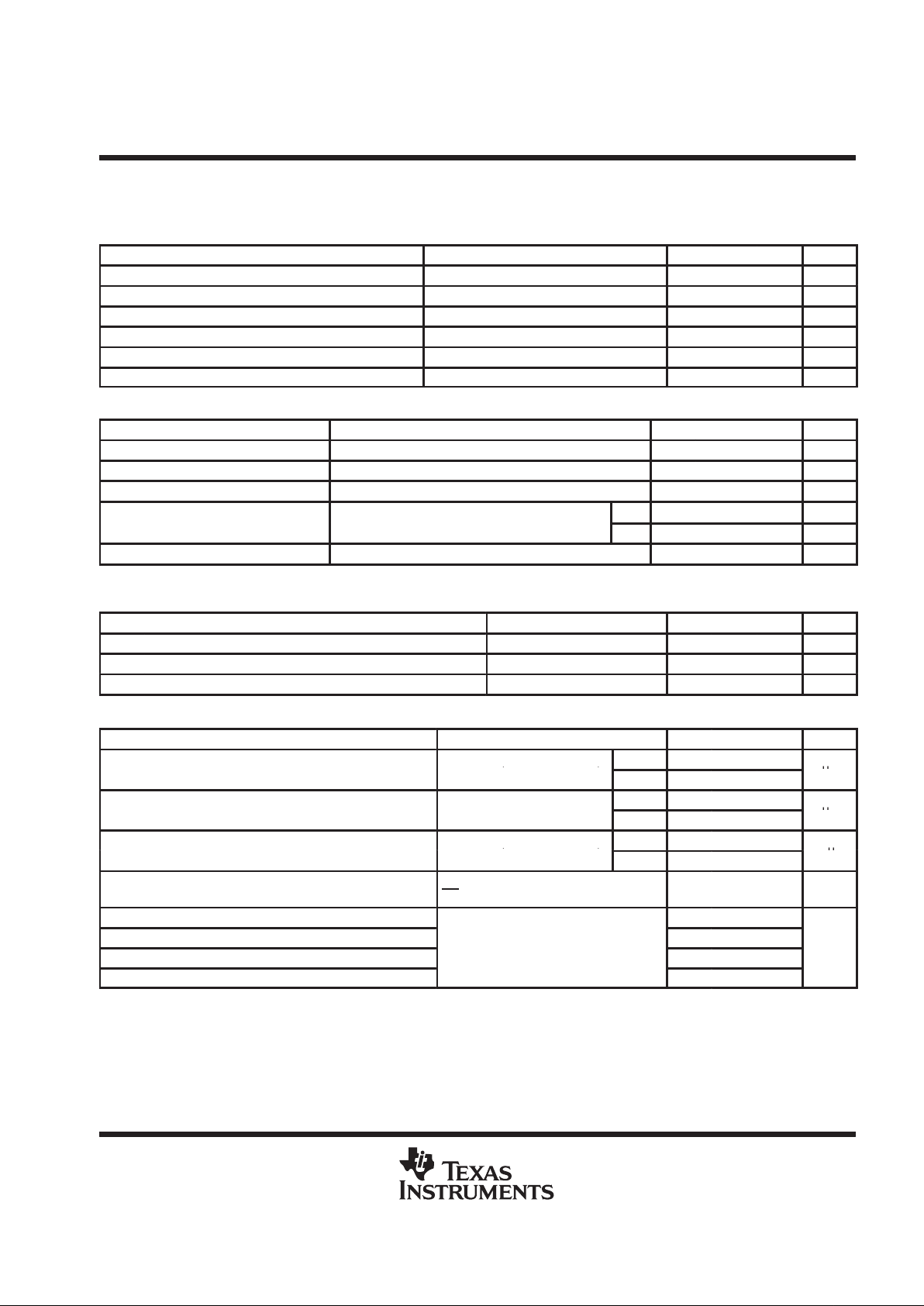
AVAILABLE OPTIONS
PACKAGE
T
A
SOIC
(D)
0°C to 70°C TLV5637CD
–40°C to 85°C TLV5637ID
Please be aware that an important notice concerning availability, standard warranty, and use in critical applications of
Texas Instruments semiconductor products and disclaimers thereto appears at the end of this data sheet.
Copyright 1999, Texas Instruments Incorporated
PRODUCTION DATA information is current as of publication date.
Products conform to specifications per the terms of Texas Instruments
standard warranty. Production processing does not necessarily include
testing of all parameters.
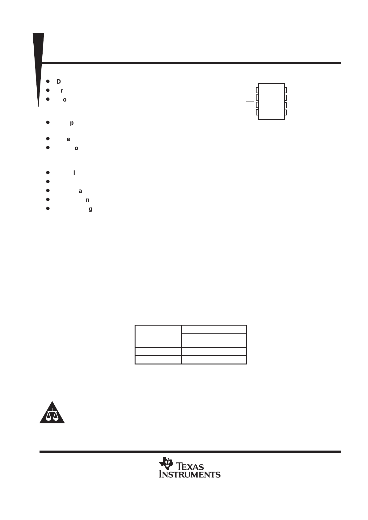
1
2
3
4
8
7
6
5
DIN
SCLK
CS
OUTA
V
DD
OUTB
REF
AGND
D PACKAGE
(TOP VIEW)
SPI and QSPI are trademarks of Motorola, Inc.
Microwire is a trademark of National Semiconductor Corporation.
TLV5637
2.7 V TO 5.5 V LOW POWER DUAL 10-BIT DIGITAL-TO-ANALOG
CONVERTER WITH INTERNAL REFERENCE AND POWER DOWN
SLAS224 –JUNE 1999
2
POST OFFICE BOX 655303 • DALLAS, TEXAS 75265
functional block diagram
Serial
Interface
and
Control
10-Bit
DAC B
Latch
SCLK
DIN
CS
OUTA
Power-On
Reset
x2
10
2-Bit
Control
Latch
Power
and Speed
Control
2
Voltage
Bandgap
PGA With
Output Enable
10-Bit
DAC A
Latch
10
REF AGND V
DD
2
10 10
OUTB
x2
Buffer
10
Terminal Functions
TERMINAL
NAME NO.
I/O/P
DESCRIPTION
AGND 5 P Ground
CS 3 I Chip select. Digital input active low, used to enable/disable inputs
DIN 1 I Digital serial data input
OUTA 4 I DAC A analog voltage output
OUTB 7 O DAC B analog voltage output
REF 6 I/O Analog reference voltage input/output
SCLK 2 I Digital serial clock input
V
DD
8 P Positive power supply
TLV5637
2.7 V TO 5.5 V LOW POWER DUAL 10-BIT DIGITAL-TO-ANALOG
CONVERTER WITH INTERNAL REFERENCE AND POWER DOWN
SLAS224 –JUNE 1999
3
POST OFFICE BOX 655303 • DALLAS, TEXAS 75265
absolute maximum ratings over operating free-air temperature range (unless otherwise noted)
†
Supply voltage (V
DD
to AGND) 7 V. . . . . . . . . . . . . . . . . . . . . . . . . . . . . . . . . . . . . . . . . . . . . . . . . . . . . . . . . . . . . . .
Reference input voltage range – 0.3 V to V
DD
+ 0.3 V. . . . . . . . . . . . . . . . . . . . . . . . . . . . . . . . . . . . . . . . . . . . . . .
Digital input voltage range – 0.3 V to V
DD
+ 0.3 V. . . . . . . . . . . . . . . . . . . . . . . . . . . . . . . . . . . . . . . . . . . . . . . . . .
Operating free-air temperature range, T
A
: TLV5637C 0°C to 70°C. . . . . . . . . . . . . . . . . . . . . . . . . . . . . . . . . . . .
TLV5637I –40°C to 85°C. . . . . . . . . . . . . . . . . . . . . . . . . . . . . . . . . . .
Storage temperature range, T
stg
–65°C to 150° C. . . . . . . . . . . . . . . . . . . . . . . . . . . . . . . . . . . . . . . . . . . . . . . . . . .
Lead temperature 1,6 mm (1/16 inch) from case for 10 seconds 260°C. . . . . . . . . . . . . . . . . . . . . . . . . . . . . . .
†
Stresses beyond those listed under “absolute maximum ratings” may cause permanent damage to the device. These are stress ratings only, and
functional operation of the device at these or any other conditions beyond those indicated under “recommended operating conditions” is not
implied. Exposure to absolute-maximum-rated conditions for extended periods may affect device reliability.
recommended operating conditions
MIN NOM MAX UNIT
pp
VDD = 5 V 4.5 5 5.5 V
Suppl
y v
oltage, V
DD
VDD = 3 V 2.7 3 3.3 V
Power on threshold voltage, POR 0.55 2 V
High-level digital input voltage, V
IH
VDD = 2.7 V to 5.5 V 2 V
Low-level digital input voltage, V
IL
VDD = 2.7 V to 5.5 V 0.8 V
Reference voltage, V
ref
to REF terminal VDD = 5 V (see Note 1) AGND 2.048 VDD–1.5 V
Reference voltage, V
ref
to REF terminal VDD = 3 V (see Note 1) AGND 1.024 VDD–1.5 V
Load resistance, R
L
2 kΩ
Load capacitance, C
L
100 pF
Clock frequency, f
CLK
20 MHz
p
p
TLV5637C 0 70
°
Operating free-air temperature, T
A
TLV5637I –40 85
°C
NOTE 1: Due to the x2 output buffer , a reference input voltage ≥ (VDD – 0.4 V)/2 causes clipping of the transfer function. The output buffer of the
internal reference must be disabled, if an external reference is used.
TLV5637
2.7 V TO 5.5 V LOW POWER DUAL 10-BIT DIGITAL-TO-ANALOG
CONVERTER WITH INTERNAL REFERENCE AND POWER DOWN
SLAS224 –JUNE 1999
4
POST OFFICE BOX 655303 • DALLAS, TEXAS 75265
electrical characteristics over recommended operating conditions (unless otherwise noted)
power supply
PARAMETER TEST CONDITIONS MIN TYP MAX
UNIT
VDD = 5 V,
Fast 4.2 5 mA
DD
Int. ref.
Slow 2 2.5 mA
VDD = 3 V,
Fast 3.7 4.6 mA
pp
No load,
p
DD
Int. ref.
Slow 1.7 2.2 mA
IDDPower supply current
All inputs
=
AGND or V
DD
,
DAC latch = 0x800
VDD = 5 V,
Fast 3.8 4.6 mA
DD
Ext. ref.
Slow 1.7 2.1 mA
VDD = 3 V,
Fast 3.4 4.2 mA
DD
Ext. ref.
Slow 1.4 1.8 mA
Power-down supply current 0.01 10 µA
pp
Zero scale, See Note 2 –65
PSRR
Power supply rejection ratio
Full scale, See Note 3 –65
dB
NOTES: 2. Power supply rejection ratio at zero scale is measured by varying VDD and is given by:
PSRR = 20 log [(EZS(VDDmax) – EZS(VDDmin))/VDDmax]
3. Power supply rejection ratio at full scale is measured by varying VDD and is given by:
PSRR = 20 log [(EG(VDDmax) – EG(VDDmin))/VDDmax]
static DAC specifications
PARAMETER TEST CONDITIONS MIN TYP MAX UNIT
Resolution 10 bits
INL Integral nonlinearity, end point adjusted See Note 4 ±0.4 ±1 LSB
DNL Differential nonlinearity See Note 5 ±0.1 ±0.5 LSB
E
ZS
Zero-scale error (offset error at zero scale) See Note 6 ±24 mV
EZS TC Zero-scale-error temperature coefficient See Note 7 10 ppm/°C
E
G
Gain error See Note 8 ±0.6
% full
scale V
EG TCGain error temperature coefficient See Note 9 10 ppm/°C
NOTES: 4. The relative accuracy or integral nonlinearity (INL) sometimes referred to as linearity error, is the maximum deviation of the output
from the line between zero and full scale excluding the effects of zero code and full-scale errors. Tested from code 32 to 4095.
5. The differential nonlinearity (DNL) sometimes referred to as differential error, is the difference between the measured and ideal 1
LSB amplitude change of any two adjacent codes. Monotonic means the output voltage changes in the same direction (or remains
constant) as a change in the digital input code.
6. Zero-scale error is the deviation from zero voltage output when the digital input code is zero.
7. Zero-scale-error temperature coefficient is given by: EZSTC = [EZS(T
max
) – EZS(T
min
)]/V
ref
× 106/(T
max
– T
min
).
8. Gain error is the deviation from the ideal output (2V
ref
– 1 LSB) with an output load of 10 k excluding the effects of the zero-error.
9. Gain temperature coefficient is given by: EGTC = [EG(T
max
) – EG (T
min
)]/V
ref
× 106/(T
max
– T
min
).
output specifications
PARAMETER TEST CONDITIONS MIN TYP MAX UNIT
V
O
Output voltage RL = 10 kΩ 0 VDD–0.4 V
Output load regulation accuracy VO = 4.096 V , 2.048 V, RL = 2 kΩ ±0.25
% full
scale V
TLV5637
2.7 V TO 5.5 V LOW POWER DUAL 10-BIT DIGITAL-TO-ANALOG
CONVERTER WITH INTERNAL REFERENCE AND POWER DOWN
SLAS224 –JUNE 1999
5
POST OFFICE BOX 655303 • DALLAS, TEXAS 75265
electrical characteristics over recommended operating conditions (unless otherwise noted)
(Continued)
reference pin configured as output (REF)
PARAMETER TEST CONDITIONS MIN TYP MAX UNIT
V
ref(OUTL)
Low reference voltage 1.003 1.024 1.045 V
V
ref(OUTH)
High reference voltage VDD > 4.75 V 2.027 2.048 2.069 V
I
ref(source)
Output source current 1 mA
I
ref(sink)
Output sink current –1 mA
Load capacitance 100 pF
PSRR Power supply rejection ratio –65 dB
reference pin configured as input (REF)
PARAMETER TEST CONDITIONS MIN TYP MAX UNIT
VIInput voltage 0 V
DD–1.5
V
RIInput resistance 10 MΩ
CIInput capacitance 5 pF
p
Fast 1.3 MHz
Reference input bandwidth
REF
= 0.2
V
pp
+ 1.
024 V dc
Slow 525 kHz
Reference feedthrough REF = 1 Vpp at 1 kHz + 1.024 V dc (see Note 10) –80 dB
NOTE 10: Reference feedthrough is measured at the DAC output with an input code = 0x000.
digital inputs
PARAMETER TEST CONDITIONS MIN TYP MAX UNIT
I
IH
High-level digital input current VI = V
DD
1 µA
I
IL
Low-level digital input current VI = 0 V –1 µA
C
i
Input capacitance 8 pF
analog output dynamic performance
PARAMETER TEST CONDITIONS MIN TYP MAX UNIT
p
R
= 10 kΩ,C
= 100 pF,
Fast 0.8 2.4
t
s(FS)
Output settling time, full scale
L
,
L
,
See Note 11
Slow 2.8 5.5
µ
s
p
R
= 10 kΩ,C
= 100 pF,
Fast 0.4 1.2
t
s(CC)
Output settling time, code to code
L
,
L
,
See Note 12
Slow 0.8 1.6
µ
s
R
= 10 kΩ,C
= 100 pF,
Fast 12
SR
Slew rate
L
,
L
,
See Note 13
Slow 1.8
V/µs
Glitch energy
DIN = 0 to 1, f
CLK
= 100 kHz,
CS
= V
DD
5 nV–S
SNR Signal-to-noise ratio 53 56
S/(N+D) Signal-to-noise + distortion
f
= 480 kSPS, f
= 1 kHz,
50 54
THD Total harmonic distortion
s
,
out
,
RL = 10 kΩ,C
L
= 100 pF
–61 –50
dB
SFDR Spurious free dynamic range 51 62
NOTES: 11. Settling time is the time for the output signal to remain within ±0.5 LSB of the final measured value for a digital input code change
of 0x020 to 0xFDF or 0xFDF to 0x020 respectively. Not tested, assured by design.
12. Settling time is the time for the output signal to remain within ± 0.5 LSB of the final measured value for a digital input code change
of one count. Not tested, assured by design.
13. Slew rate determines the time it takes for a change of the DAC output from 10% to 90% full-scale voltage.
TLV5637
2.7 V TO 5.5 V LOW POWER DUAL 10-BIT DIGITAL-TO-ANALOG
CONVERTER WITH INTERNAL REFERENCE AND POWER DOWN
SLAS224 –JUNE 1999
6
POST OFFICE BOX 655303 • DALLAS, TEXAS 75265
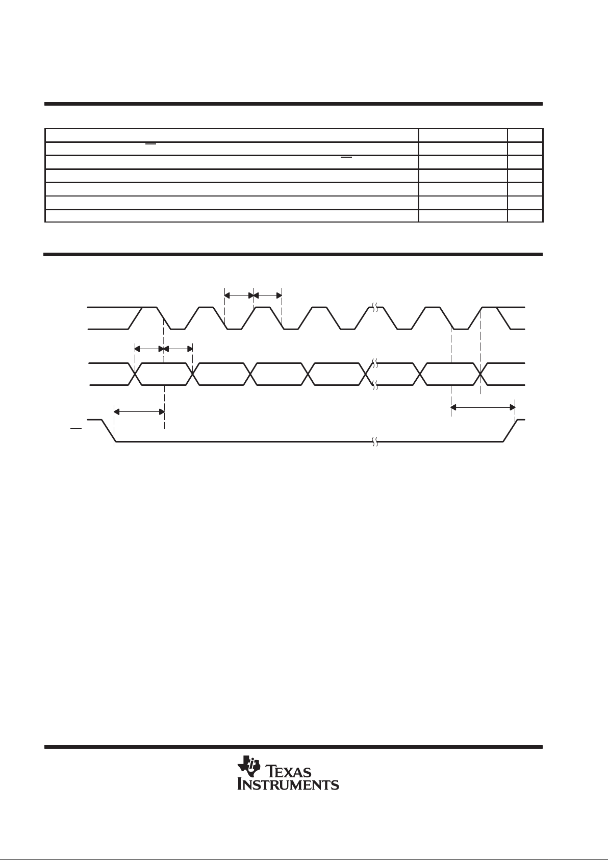
digital input timing requirements
MIN NOM MAX UNIT
t
su(CS–CK)
Setup time, CS low before first negative SCLK edge 10 ns
t
su(C16-CS)
Setup time, 16th negative SCLK edge (when D0 is sampled) before CS rising edge 10 ns
t
wH
SCLK pulse width high 25 ns
t
wL
SCLK pulse width low 25 ns
t
su(D)
Setup time, data ready before SCLK falling edge 10 ns
t
h(D)
Hold time, data held valid after SCLK falling edge 5 ns
PARAMETER MEASUREMENT INFORMATION
t
wL
SCLK
CS
DIN
D15 D14 D13 D12 D1 D0 XX
1
X
2 3 4 5 15 16
X
t
wH
t
su(D)th(D)
t
su(CS-CK)
t
su(C16-CS)
Figure 1. Timing Diagram

TLV5637
2.7 V TO 5.5 V LOW POWER DUAL 10-BIT DIGITAL-TO-ANALOG
CONVERTER WITH INTERNAL REFERENCE AND POWER DOWN
SLAS224 –JUNE 1999
7
POST OFFICE BOX 655303 • DALLAS, TEXAS 75265
TYPICAL CHARACTERISTICS
Figure 2
Fast Mode
Slow Mode
VDD = 5 V
V
ref
= Int. 2 V
Input Code = 1023 (Both DACs)
2.5
2
1
0.5
–40–30 –20–10 0 10 20
– Supply Current – mA
3
4
SUPPLY CURRENT
vs
FREE-AIR TEMPERATURE
4.5
30 40 50 90
3.5
1.5
60 70 80
I
DD
TA – Free-Air Temperature – °C
Figure 3
Fast Mode
Slow Mode
VDD = 3 V
V
ref
= Int. 1 V
Input Code = 1023 (Both DACs)
2.5
2
1
0.5
–40–30 –20–10 0 10 20
– Supply Current – mA
3
4
SUPPLY CURRENT
vs
FREE-AIR TEMPERATURE
4.5
30 40 50 90
3.5
1.5
60 70 80
I
DD
TA – Free-Air Temperature – °C
Figure 4
1.4
1
0.4
0
010203040
– Power Down Supply Current – mA
2.2
2.4
POWER DOWN SUPPLY CURRENT
vs
TIME
2.6
50 60 70 80
2
1.8
1.6
1.2
0.8
0.6
0.2
t – Time – µs
I
DD
Figure 5
2.058
2.054
2.052
2.05
0 0.5 1 1.5 2 2.5 3
– Output Voltage – V
2.06
2.062
Source Current – mA
OUTPUT VOLTAGE
vs
LOAD CURRENT
2.064
3.5 4
2.056
V
O
Fast Mode
Slow Mode
VDD = 3 V
V
ref
= Int. 1 V
Input Code = 4095

TLV5637
2.7 V TO 5.5 V LOW POWER DUAL 10-BIT DIGITAL-TO-ANALOG
CONVERTER WITH INTERNAL REFERENCE AND POWER DOWN
SLAS224 –JUNE 1999
8
POST OFFICE BOX 655303 • DALLAS, TEXAS 75265
TYPICAL CHARACTERISTICS
Figure 6
4.122
4.12
4.116
4.114
0 0.5 1 1.5 2 2.5 3
4.124
4.126
4.128
3.5 4
4.118
– Output Voltage – V
Source Current – mA
OUTPUT VOLTAGE
vs
LOAD CURRENT
V
O
Fast Mode
Slow Mode
VDD = 5 V
V
ref
= Int. 2 V
Input Code = 4095
Figure 7
1.5
1
0.5
0
0 0.5 1 1.5 2 2.5 3
2
2.5
3
3.5 4
– Output Voltage – V
Sink Current – mA
OUTPUT VOLTAGE
vs
LOAD CURRENT
V
O
Fast Mode
Slow Mode
VDD = 3 V
V
ref
= Int. 1 V
Input Code = 0
Figure 8
3.5
2
1
0
0 0.5 1 1.5 2 2.5 3
4
4.5
5
3.5 4
3
2.5
1.5
0.5
– Output Voltage – V
Sink Current – mA
OUTPUT VOLTAGE
vs
LOAD CURRENT
V
O
Fast Mode
Slow Mode
VDD = 5 V
V
ref
= Int. 2 V
Input Code = 0
Figure 9
–40
–50
–80
–100
100 1000
THD+N – Total Harmonic Distortion and Noise – dB
–20
–10
f – Frequency – Hz
TOTAL HARMONIC DISTORTION AND NOISE
vs
FREQUENCY
0
10000 10000
0
–30
–60
–70
–90
Fast Mode
Slow Mode
VDD = 5 V
V
ref
= 1 V dc + 1 V p/p Sinewave
Output Full Scale

TLV5637
2.7 V TO 5.5 V LOW POWER DUAL 10-BIT DIGITAL-TO-ANALOG
CONVERTER WITH INTERNAL REFERENCE AND POWER DOWN
SLAS224 –JUNE 1999
9
POST OFFICE BOX 655303 • DALLAS, TEXAS 75265
TYPICAL CHARACTERISTICS
–40
–50
–80
–100
100 1000
THD – Total Harmonic Distortion – dB
–20
–10
f – Frequency – Hz
TOTAL HARMONIC DISTORTION
vs
FREQUENCY
0
10000 100000
–30
–60
–70
–90
Fast Mode
Slow Mode
VDD = 5 V
V
ref
= 1 V dc + 1 V p/p Sinewave
Output Full Scale
Figure 10
–0.4
–1
0 256 512
INL – Integral Nonlinearity Error – LSB
0
0.6
Digital Code
INTEGRAL NONLINEARITY ERROR
1
768 1024
0.8
0.4
0.2
–0.2
–0.6
–0.8
Figure 11

TLV5637
2.7 V TO 5.5 V LOW POWER DUAL 10-BIT DIGITAL-TO-ANALOG
CONVERTER WITH INTERNAL REFERENCE AND POWER DOWN
SLAS224 –JUNE 1999
10
POST OFFICE BOX 655303 • DALLAS, TEXAS 75265
TYPICAL CHARACTERISTICS
–0.1
–0.2
0 256 512
DNL – Differential Nonlinearity Error – LSB
0
0.15
Digital Code
DIFFERENTIAL NONLINEARITY ERROR
0.2
768 1024
0.1
0.05
–0.05
–0.15
Figure 12
APPLICATION INFORMATION
general function
The TL V5637 is a dual 10-bit, single supply DAC, based on a resistor string architecture. It consists of a serial
interface, a speed and power-down control logic, a programmable internal reference, a resistor string, and a
rail-to-rail output buffer.
The output voltage (full scale determined by reference) is given by:
2REF
CODE
0x1000
[V]
Where REF is the reference voltage and CODE is the digital input value in the range 0x000 to 0xFFF . Because
it is a 10-bit DAC, only D1 1 to D2 are used. D0 and D1 are ignored. A power on reset initially puts the internal
latches to a defined state (all bits zero).
serial interface
A falling edge of CS starts shifting the data bit-per-bit (starting with the MSB) to the internal register on the falling
edges of SCLK. After 16 bits have been transferred or CS
rises, the content of the shift register is moved to the
target latches (DAC A, DAC B, BUFFER, CONTROL), depending on the control bits within the data word.
Figure 13 shows examples of how to connect the TLV5637 to TMS320, SPI, and Microwire.
TMS320
DSP
FSX
CLKX
DX
TLV5637
SCLK
DIN
CS
SPI
I/O
SCK
MOSI
TLV5637
SCLK
DIN
CS
Microwire
I/O
SK
SO
TLV5637
SCLK
DIN
CS
Figure 13. Three-Wire Interface
Notes on SPI and Microwire: Before the controller starts the data transfer, the software has to generate a
falling edge on the I/O pin connected to CS
. If the word width is 8 bits (SPI and Microwire), two write
operations must be performed to program the TL V5637. After the write operation(s), the holding registers or the
control register are updated automatically on the 16
th
positive clock edge.

TLV5637
2.7 V TO 5.5 V LOW POWER DUAL 10-BIT DIGITAL-TO-ANALOG
CONVERTER WITH INTERNAL REFERENCE AND POWER DOWN
SLAS224 –JUNE 1999
11
POST OFFICE BOX 655303 • DALLAS, TEXAS 75265
APPLICATION INFORMATION
serial clock frequency and update rate
The maximum serial clock frequency is given by:
f
sclkmax
+
1
t
whmin
)
t
wlmin
+
20 MHz
The maximum update rate is:
f
updatemax
+
1
16ǒt
whmin
)
t
wlmin
Ǔ
+
1.25 MHz
Note, that the maximum update rate is just a theoretical value for the serial interface, as the settling time of the
TLV5637 has to be considered, too.
data format
The 16-bit data word for the TLV5637 consists of two parts:
D
Program bits (D15..D12)
D
New data (D11..D0)
D15 D14 D13 D12 D11 D10 D9 D8 D7 D6 D5 D4 D3 D2 D1 D0
R1 SPD PWR R0 12 Data bits
SPD: Speed control bit 1 → fast mode 0 → slow mode
PWR: Power control bit 1 → power down 0 → normal operation
The following table lists the possible combination of the register select bits:
register select bits
R1 R0 REGISTER
0 0 Write data to DAC B and BUFFER
0 1 Write data to BUFFER
1 0 Write data to DAC A and update DAC B with BUFFER content
1 1 Write data to control register
The meaning of the 12 data bits depends on the register. If one of the DAC registers or the BUFFER is selected,
then the 12 data bits determine the new DAC value:
data bits: DAC A, DAC B and BUFFER
D11 D10 D9 D8 D7 D6 D5 D4 D3 D2 D1 D0
New DAC Value 0 0
If control is selected, then D1, D0 of the 12 data bits are used to program the reference voltage:
data bits: CONTROL
D11 D10 D9 D8 D7 D6 D5 D4 D3 D2 D1 D0
X X X X X X X X X X REF1 REF0
X: don’t care
REF1 and REF0 determine the reference source and, if internal reference is selected, the reference voltage.

TLV5637
2.7 V TO 5.5 V LOW POWER DUAL 10-BIT DIGITAL-TO-ANALOG
CONVERTER WITH INTERNAL REFERENCE AND POWER DOWN
SLAS224 –JUNE 1999
12
POST OFFICE BOX 655303 • DALLAS, TEXAS 75265
APPLICATION INFORMATION
reference bits
REF1 REF0 REFERENCE
0 0 External
0 1 1.024 V
1 0 2.048 V
1 1 External
CAUTION:
If external reference voltage is applied to the REF pin, external reference MUST be selected.
examples of operation:
D
Set DAC A output, select fast mode, select internal reference at 2.048 V:
1. Set reference voltage to 2.048 V (CONTROL register):
D15 D14 D13 D12 D11 D10 D9 D8 D7 D6 D5 D4 D3 D2 D1 D0
1 1 0 1 0 0 0 0 0 0 0 0 0 0 1 0
2. Write new DAC A value and update DAC A output:
D15 D14 D13 D12 D11 D10 D9 D8 D7 D6 D5 D4 D3 D2 D1 D0
1 1 0 0 New DAC A output value 0 0
The DAC A output is updated on the rising clock edge after D0 is sampled.
T o output data consecutively using the same DAC configuration, it is not necessary to program the CONTROL
register again.
D
Set DAC B output, select fast mode, select external reference:
3. Select external reference (CONTROL register):
D15 D14 D13 D12 D11 D10 D9 D8 D7 D6 D5 D4 D3 D2 D1 D0
1 1 0 1 0 0 0 0 0 0 0 0 0 0 0 0
4. Write new DAC B value to BUFFER and update DAC B output:
D15 D14 D13 D12 D11 D10 D9 D8 D7 D6 D5 D4 D3 D2 D1 D0
0 1 0 0 New BUFFER content and DAC B output value 0 0
X = Don’t care
The DAC A output is updated on the rising clock edge after D0 is sampled.
T o output data consecutively using the same DAC configuration, it is not necessary to program the CONTROL
register again.

TLV5637
2.7 V TO 5.5 V LOW POWER DUAL 10-BIT DIGITAL-TO-ANALOG
CONVERTER WITH INTERNAL REFERENCE AND POWER DOWN
SLAS224 –JUNE 1999
13
POST OFFICE BOX 655303 • DALLAS, TEXAS 75265
APPLICATION INFORMATION
examples of operation: (continued)
D
Set DAC A value, set DAC B value, update both simultaneously , select slow mode, select internal reference
at 1.024 V:
1. Set reference voltage to 1.024 V (CONTROL register):
D15 D14 D13 D12 D11 D10 D9 D8 D7 D6 D5 D4 D3 D2 D1 D0
1 0 0 1 0 0 0 0 0 0 0 0 0 0 0 1
2. Write data for DAC B to BUFFER:
D15 D14 D13 D12 D11 D10 D9 D8 D7 D6 D5 D4 D3 D2 D1 D0
0 0 0 1 New DAC B value 0 0
X = Don’t care
3. Write new DAC A value and update DAC A and B simultaneously:
D15 D14 D13 D12 D11 D10 D9 D8 D7 D6 D5 D4 D3 D2 D1 D0
1 0 0 0 New DAC A value 0 0
X = Don’t care
Both outputs are updated on the rising clock edge after D0 from the DAC A data word is sampled.
D
Set power down mode:
D15 D14 D13 D12 D11 D10 D9 D8 D7 D6 D5 D4 D3 D2 D1 D0
X X 1 X X X X X X X X X X X X X
X = Don’t care

TLV5637
2.7 V TO 5.5 V LOW POWER DUAL 10-BIT DIGITAL-TO-ANALOG
CONVERTER WITH INTERNAL REFERENCE AND POWER DOWN
SLAS224 –JUNE 1999
14
POST OFFICE BOX 655303 • DALLAS, TEXAS 75265
APPLICATION INFORMATION
linearity, offset, and gain error using single ended supplies
When an amplifier is operated from a single supply , the voltage offset can still be either positive or negative. With
a positive offset, the output voltage changes on the first code change. With a negative offset, the output voltage
may not change with the first code, depending on the magnitude of the offset voltage.
The output amplifier attempts to drive the output to a negative voltage. However, because the most negative
supply rail is ground, the output cannot drive below ground and clamps the output at 0 V.
The output voltage then remains at zero until the input code value produces a sufficient positive output voltage
to overcome the negative offset voltage, resulting in the transfer function shown in Figure 14.
DAC Code
Output
Voltage
0 V
Negative
Offset
Figure 14. Effect of Negative Offset (Single Supply)
This offset error , not the linearity error, produces this breakpoint. The transfer function would have followed the
dotted line if the output buffer could drive below the ground rail.
For a DAC, linearity is measured between zero-input code (all inputs 0) and full-scale code (all inputs 1) after
offset and full scale are adjusted out or accounted for in some way . However , single supply operation does not
allow for adjustment when the offset is negative due to the breakpoint in the transfer function. So the linearity
is measured between full-scale code and the lowest code that produces a positive output voltage.

TLV5637
2.7 V TO 5.5 V LOW POWER DUAL 10-BIT DIGITAL-TO-ANALOG
CONVERTER WITH INTERNAL REFERENCE AND POWER DOWN
SLAS224 –JUNE 1999
15
POST OFFICE BOX 655303 • DALLAS, TEXAS 75265
APPLICATION INFORMATION
definitions of specifications and terminology
integral nonlinearity (INL)
The relative accuracy or integral nonlinearity (INL), sometimes referred to as linearity error, is the maximum
deviation of the output from the line between zero and full scale excluding the effects of zero code and full-scale
errors.
differential nonlinearity (DNL)
The differential nonlinearity (DNL), sometimes referred to as differential error, is the difference between the
measured and ideal 1 LSB amplitude change of any two adjacent codes. Monotonic means the output voltage
changes in the same direction (or remains constant) as a change in the digital input code.
zero-scale error (E
ZS
)
Zero-scale error is defined as the deviation of the output from 0 V at a digital input value of 0.
gain error (E
G
)
Gain error is the error in slope of the DAC transfer function.
signal-to-noise ratio + distortion (S/N+D)
S/N+D is the ratio of the rms value of the measured input signal to the rms sum of all other spectral components
below the Nyquist frequency, including harmonics but excluding dc. The value for S/N+D is expressed in
decibels.
spurious free dynamic range (SFDR)
Spurious free dynamic range is the difference between the rms value of the output signal and the rms value of
the spurious signal within a specified bandwidth. The value for SFDR is expressed in decibels.

TLV5637
2.7 V TO 5.5 V LOW POWER DUAL 10-BIT DIGITAL-TO-ANALOG
CONVERTER WITH INTERNAL REFERENCE AND POWER DOWN
SLAS224 –JUNE 1999
16
POST OFFICE BOX 655303 • DALLAS, TEXAS 75265
MECHANICAL DATA
D (R-PDSO-G**) PLASTIC SMALL-OUTLINE PACKAGE
14 PINS SHOWN
4040047/D 10/96
0.228 (5,80)
0.244 (6,20)
0.069 (1,75) MAX
0.010 (0,25)
0.004 (0,10)
1
14
0.014 (0,35)
0.020 (0,51)
A
0.157 (4,00)
0.150 (3,81)
7
8
0.044 (1,12)
0.016 (0,40)
Seating Plane
0.010 (0,25)
PINS **
0.008 (0,20) NOM
A MIN
A MAX
DIM
Gage Plane
0.189
(4,80)
(5,00)
0.197
8
(8,55)
(8,75)
0.337
14
0.344
(9,80)
16
0.394
(10,00)
0.386
0.004 (0,10)
M
0.010 (0,25)
0.050 (1,27)
0°–8°
NOTES: A. All linear dimensions are in inches (millimeters).
B. This drawing is subject to change without notice.
C. Body dimensions do not include mold flash or protrusion, not to exceed 0.006 (0,15).
D. Falls within JEDEC MS-012

IMPORTANT NOTICE
T exas Instruments and its subsidiaries (TI) reserve the right to make changes to their products or to discontinue
any product or service without notice, and advise customers to obtain the latest version of relevant information
to verify, before placing orders, that information being relied on is current and complete. All products are sold
subject to the terms and conditions of sale supplied at the time of order acknowledgement, including those
pertaining to warranty, patent infringement, and limitation of liability.
TI warrants performance of its semiconductor products to the specifications applicable at the time of sale in
accordance with TI’s standard warranty. Testing and other quality control techniques are utilized to the extent
TI deems necessary to support this warranty. Specific testing of all parameters of each device is not necessarily
performed, except those mandated by government requirements.
CERT AIN APPLICATIONS USING SEMICONDUCTOR PRODUCTS MAY INVOLVE POTENTIAL RISKS OF
DEATH, PERSONAL INJURY, OR SEVERE PROPERTY OR ENVIRONMENTAL DAMAGE (“CRITICAL
APPLICATIONS”). TI SEMICONDUCTOR PRODUCTS ARE NOT DESIGNED, AUTHORIZED, OR
WARRANTED TO BE SUITABLE FOR USE IN LIFE-SUPPORT DEVICES OR SYSTEMS OR OTHER
CRITICAL APPLICATIONS. INCLUSION OF TI PRODUCTS IN SUCH APPLICA TIONS IS UNDERST OOD TO
BE FULLY AT THE CUSTOMER’S RISK.
In order to minimize risks associated with the customer’s applications, adequate design and operating
safeguards must be provided by the customer to minimize inherent or procedural hazards.
TI assumes no liability for applications assistance or customer product design. TI does not warrant or represent
that any license, either express or implied, is granted under any patent right, copyright, mask work right, or other
intellectual property right of TI covering or relating to any combination, machine, or process in which such
semiconductor products or services might be or are used. TI’s publication of information regarding any third
party’s products or services does not constitute TI’s approval, warranty or endorsement thereof.
Copyright 1999, Texas Instruments Incorporated
 Loading...