

Datasheet TLV5633IPWR, TLV5633IDWR, TLV5633IPW, TLV5633CPWR, TLV5633IDW Datasheet (Texas Instruments)
...
TLV5633C, TLV5633I
2.7 V TO 5.5 V LOW POWER 12-BIT DIGITAL-TO-ANALOG
CONVERTERS WITH INTERNAL REFERENCE AND POWER DOWN
SLAS190 – MARCH 1999
D
12-Bit Voltage Output DAC
D
Programmable Internal Reference
D
Programmable Settling Time vs Power
Consumption
1 µs in Fast Mode
3.5 µs in Slow Mode
D
8-Bit µController Compatible Interface
D
Differential Nonlinearity . . . <0.5 LSB Typ
D
Voltage Output Range ... 2x the
Reference V oltage
D
Monotonic Over Temperature
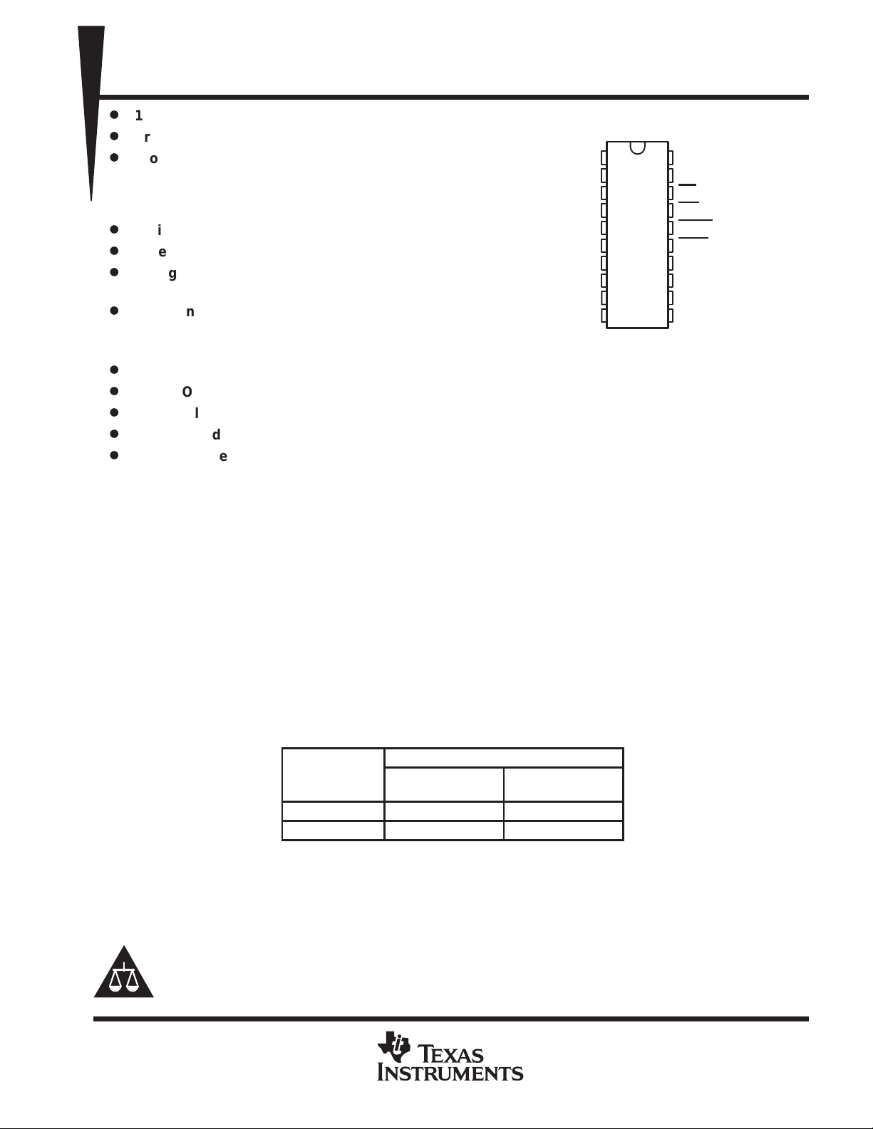
DW OR PW PACKAGE
(TOP VIEW)
1
2
3
4
5
6
7
8
9
10
20
19
18
17
16
15
14
13
12
11
DV
D2
D3
D4
D5
D6
D7
A1
A0
SPD
DD
D1
D0
CS
WE
LDAC
PWR
AGND
OUT
REF
AV
DD
applications
D
Digital Servo Control Loops
D
Digital Offset and Gain Adjustment
D
Industrial Process Control
D
Machine and Motion Control Devices
D
Mass Storage Devices
description
The TLV5633 is a 12-bit voltage output digital-to-analog converter (DAC) with an 8-bit microcontroller
compatible parallel interface. The 8 LSBs, the 4 MSBs, and 5 control bits are written using three different
addresses. Developed for a wide range of supply voltages, the TL V5633 can be operated from 2.7 V to 5.5 V.
The resistor string output voltage is buffered by a x2 gain rail-to-rail output buffer . The buffer features a Class A
(slow mode: AB) output stage to improve stability and reduce settling time. The programmable settling time of
the DAC allows the designer to optimize speed versus power dissipation. With its on-chip programmable
precision voltage reference, the TL V5633 simplifies overall system design. Because of its ability to source up
to 1 mA, the internal reference can also be used as a system reference. The settling time and the reference
voltage can be chosen by a control register.
Implemented with a CMOS process, the device is designed for single supply operation from 2.7 V to 5.5 V. It
is available in 20-pin SOIC and TSSOP packages in standard commercial and industrial temperature ranges.
AVAILABLE OPTIONS
PACKAGE
T
A
0°C to 70°C TLV5633CDW TLV5633CPW
–40°C to 85°C TLV5633IDW TLV5633IPW
Please be aware that an important notice concerning availability, standard warranty, and use in critical applications of
Texas Instruments semiconductor products and disclaimers thereto appears at the end of this data sheet.
SOIC
(DW)
TSSOP
(PW)
PRODUCTION DATA information is current as of publication date.
Products conform to specifications per the terms of Texas Instruments
standard warranty. Production processing does not necessarily include
testing of all parameters.
POST OFFICE BOX 655303 • DALLAS, TEXAS 75265
Copyright 1999, Texas Instruments Incorporated
1
TLV5633C, TLV5633I
I/O/P
DESCRIPTION
2.7 V TO 5.5 V LOW POWER 12-BIT DIGITAL-TO-ANALOG
CONVERTERS WITH INTERNAL REFERENCE AND POWER DOWN
SLAS190 – MARCH 1999
functional block diagram
SPD
PWR
A(0,1)
CS
WE
2
Power-On
Reset
Interface
Control
5
5-Bit
Control
Latch
4
4-Bit
DAC MSW
Holding
Latch
8 8
8-Bit
DAC LSW
Holding
Latch
Voltage
Bandgap
Powerdown
and Speed
Control
2
4
REF AGND DV
PGA With
Output Enable
12 12
12-Bit
DAC
Register
DD
x2
AV
DD
OUT
D(0–7)
LDAC
Terminal Functions
TERMINAL
NAME NO.
A1, A0 7, 8 I Address input
AGND 14 P Ground
AV
DD
CS 18 I Chip select. Digital input active low, used to enable/disable inputs
D0 – D1 19, 20 I Data input
D2 – D7 1–6 I Data input
DV
DD
LDAC 16 I Load DAC. Digital input active low, used to load DAC output
OUT 13 O DAC analog voltage output
PWR 15 I Power down. Digital input active low
REF 12 I/O Analog reference voltage input/output
SPD 9 I Speed select. Digital input
WE 17 I Write enable. Digital input active low , used to latch data
11 P Positive power supply (analog part)
10 P Positive power supply (digital part)
2
POST OFFICE BOX 655303 • DALLAS, TEXAS 75265
Suppl
oltage, DV
AV
Operating free-air temperature, T
°C
TLV5633C, TLV5633I
2.7 V TO 5.5 V LOW POWER 12-BIT DIGITAL-TO-ANALOG
CONVERTERS WITH INTERNAL REFERENCE AND POWER DOWN
SLAS190 – MARCH 1999
absolute maximum ratings over operating free-air temperature range (unless otherwise noted)
Supply voltage (DV
Supply voltage difference range, AVDD – DVDD – 2.8 V to 2.8 V. . . . . . . . . . . . . . . . . . . . . . . . . . . . . . . . . . . . . .
Reference input voltage range – 0.3 V to VDD + 0.3 V. . . . . . . . . . . . . . . . . . . . . . . . . . . . . . . . . . . . . . . . . . . . . . .
Digital input voltage range – 0.3 V to VDD + 0.3 V. . . . . . . . . . . . . . . . . . . . . . . . . . . . . . . . . . . . . . . . . . . . . . . . . .
Operating free-air temperature range, TA: TLV5633C 0°C to 70°C. . . . . . . . . . . . . . . . . . . . . . . . . . . . . . . . . . . .
Storage temperature range, T
Lead temperature 1,6 mm (1/16 inch) from case for 10 seconds 260°C. . . . . . . . . . . . . . . . . . . . . . . . . . . . . . .
†
Stresses beyond those listed under “absolute maximum ratings” may cause permanent damage to the device. These are stress ratings only, and
functional operation of the device at these or any other conditions beyond those indicated under “recommended operating conditions” is not
implied. Exposure to absolute-maximum-rated conditions for extended periods may affect device reliability.
, AVDD to AGND) 7 V. . . . . . . . . . . . . . . . . . . . . . . . . . . . . . . . . . . . . . . . . . . . . . . . . . . . . . .
DD
TLV5633I –40°C to 85°C. . . . . . . . . . . . . . . . . . . . . . . . . . . . . . . . . . .
–65°C to 150°C. . . . . . . . . . . . . . . . . . . . . . . . . . . . . . . . . . . . . . . . . . . . . . . . . . .
stg
recommended operating conditions
MIN NOM MAX UNIT
pp
y v
Supply voltage difference, ∆VDD = AVDD – DV
Power on reset voltage, POR 0.55 2 V
High-level digital input voltage, V
Low-level digital input voltage, V
Reference voltage, V
Reference voltage, V
Load resistance, R
Load capacitance, C
p
NOTE 1: Due to the x2 output buffer , a reference input voltage ≥ AV
reference must be disabled, if an external reference is used.
,
DD
DD
DD
IH
IL
to REF terminal (5-V supply), See Note 1 AGND 2.048 AVDD–1.5 V
ref
to REF terminal (3-V supply), See Note 1 AGND 1.024 AVDD–1.5 V
ref
L
L
p
A
5-V operation 4.5 5 5.5 V
3-V operation 2.7 3 3.3 V
0 0 0 V
2 DV
DD
0 0.8 V
2 kΩ
100 pF
TLV5633C 0 70
TLV5633I –40 85
causes clipping of the transfer function. The output buffer of the internal
DD/2
V
°
†
POST OFFICE BOX 655303 • DALLAS, TEXAS 75265
3
TLV5633C, TLV5633I
REF on
DD
,
REF off
IDDPower supply current
All inputs
AGND or DV
REF on
DD
,
REF off
PSRR
Power supply rejection ratio
dB
2.7 V TO 5.5 V LOW POWER 12-BIT DIGITAL-TO-ANALOG
CONVERTERS WITH INTERNAL REFERENCE AND POWER DOWN
SLAS190 – MARCH 1999
electrical characteristics over recommended operating free-air temperature range, V
= 1.024 V (unless otherwise noted)
V
ref
= 2.048 V,
ref
power supply
PARAMETER TEST CONDITIONS MIN TYP MAX
AV
= 5 V,
DVDD = 5 V
No load,
p
pp
DAC latch = 0x800
Power down supply current 0.01 1 µA
pp
NOTES: 2. Power supply rejection ratio at zero scale is measured by varying AVDD and is given by:
PSRR = 20 log [(EZS(AVDDmax) – EZS(AVDDmin))/AVDDmax]
3. Power supply rejection ratio at full scale is measured by varying AVDD and is given by:
PSRR = 20 log [(EG(AVDDmax) – EG(AVDDmin))/AVDDmax]
Zero scale, external reference, See Note 2 –60
Full scale, external reference, See Note 3 –60
=
DD
,
AV
= 3 V,
DVDD = 3 V
Fast 2.3 2.8 mA
Slow 1.3 1.6 mA
Fast 1.9 2.4 mA
Slow 0.9 1.2 mA
Fast 2.1 2.6 mA
Slow 1.2 1.5 mA
Fast 1.8 2.3 mA
Slow 0.9 1.1 mA
UNIT
static DAC specifications
PARAMETER TEST CONDITIONS MIN TYP MAX UNIT
Resolution 12 bits
INL Integral nonlinearity, end point adjusted RL = 10 kΩ, CL = 100 pF, See Note 4 ±1.2 ±3 LSB
DNL Differential nonlinearity RL = 10 kΩ, CL = 100 pF, See Note 5 ±0.3 ±0.5 LSB
E
ZS
EZS TC Zero-scale-error temperature coefficient See Note 7 20 ppm/°C
E
G
EG TC Gain error temperature coefficient See Note 9 20 ppm/°C
NOTES: 4. The relative accuracy or integral nonlinearity (INL) sometimes referred to as linearity error, is the maximum deviation of the output
Zero-scale error (offset error at zero scale) See Note 6 ±12 mV
min
% full
scale V
).
Gain error See Note 8 ±0.3
from the line between zero and full scale excluding the effects of zero code and full-scale errors (see text).
5. The differential nonlinearity (DNL) sometimes referred to as differential error, is the difference between the measured and ideal 1
LSB amplitude change of any two adjacent codes. Monotonic means the output voltage changes in the same direction (or remains
constant) as a change in the digital input code.
6. Zero-scale error is the deviation from zero voltage output when the digital input code is zero (see text).
7. Zero-scale-error temperature coefficient is given by: EZSTC = [EZS(T
8. Gain error is the deviation from the ideal output (2V
9. Gain temperature coefficient is given by: EGTC = [EG(T
– 1 LSB) with an output load of 10 kΩ excluding the effects of the zero-error .
ref
max
) – EG (T
max
min
) – EZS(T
)]/2V
ref
min
× 106/(T
)]/2V
max
× 106/(T
ref
– T
min
– T
max
).
output specifications
PARAMETER TEST CONDITIONS MIN TYP MAX UNIT
V
O
Output voltage RL = 10 kΩ AVDD–0.4 V
Output load regulation accuracy VO = 4.096 V, 2.048 V, RL = 2 kΩ ±0.29
% full
scale V
4
POST OFFICE BOX 655303 • DALLAS, TEXAS 75265
Reference input bandwidth
REF
V
024 V dc
kH
10 kH
dB
in ut
50 kH
dB
TLV5633C, TLV5633I
2.7 V TO 5.5 V LOW POWER 12-BIT DIGITAL-TO-ANALOG
CONVERTERS WITH INTERNAL REFERENCE AND POWER DOWN
SLAS190 – MARCH 1999
electrical characteristics over recommended operating free-air temperature range, V
= 1.024 V (unless otherwise noted) (Continued)
V
ref
= 2.048 V,
ref
reference pin configured as output (REF)
PARAMETER TEST CONDITIONS MIN TYP MAX UNIT
V
ref(OUTL)
V
ref(OUTH)
I
ref(source)
I
ref(sink)
PSRR Power supply rejection ratio –48 dB
Low reference voltage 1.003 1.024 1.045 V
High reference voltage AVDD = DVDD > 4.75 V 2.027 2.048 2.069 V
Output source current 1 mA
Output sink current –1 mA
reference pin configured as input (REF)
PARAMETER TEST CONDITIONS MIN TYP MAX UNIT
VIInput voltage 0 AV
RIInput resistance 10 MΩ
CIInput capacitance 5 pF
p
Harmonic distortion, reference
p
Reference feedthrough REF = 1 Vpp at 1 kHz + 1.024 V dc (see Note 10) –80 dB
NOTE 10: Reference feedthrough is measured at the DAC output with an input code = 0x000.
= 0.2
REF = 1 Vpp + 2.048 V dc, AVDD = 5 V
pp
+ 1.
100 kHz Fast –66 dB
Fast 900
Slow 500
Fast –87
z
Slow –77
Fast –74
z
Slow –61
DD–1.5
V
z
digital inputs
I
I
C
High-level digital input current VI = DV
IH
Low-level digital input current VI = 0 V –1 µA
IL
Input capacitance 8 pF
I
PARAMETER TEST CONDITIONS MIN TYP MAX UNIT
DD
1 µA
POST OFFICE BOX 655303 • DALLAS, TEXAS 75265
5
TLV5633C, TLV5633I
t
Output settling time, full scale
L
,
L
,
s
t
Output settling time, code to code
L
,
L
,
s
SR
Slew rate
L
,
L
,
V/µs
s
,
B
,
out
,
dB
2.7 V TO 5.5 V LOW POWER 12-BIT DIGITAL-TO-ANALOG
CONVERTERS WITH INTERNAL REFERENCE AND POWER DOWN
SLAS190 – MARCH 1999
operating characteristics over recommended operating free-air temperature range, V
and V
= 1.024 V, (unless otherwise noted)
ref
= 2.048 V ,
ref
analog output dynamic performance
PARAMETER TEST CONDITIONS MIN TYP MAX UNIT
R
s(FS)
s(CC)
SNR Signal-to-noise ratio 73 78
SINAD Signal-to-noise + distortion
THD Total harmonic distortion
SFDR Spurious free dynamic range 63 74
NOTES: 11. Settling time is the time for the output signal to remain within ±0.5 LSB of the final measured value for a digital input code change
p
p
Glitch energy
of 0x020 to 0xFDF or 0xFDF to 0x020 respectively.
12. Settling time is the time for the output signal to remain within ± 0.5 LSB of the final measured value for a digital input code change
of one count.
13. Slew rate determines the time it takes for a change of the DAC output from 10% to 90% full-scale voltage.
= 10 kΩ,C
See Note 11
R
= 10 kΩ,C
See Note 12
R
= 10 kΩ,C
See Note 13
DIN = 0 to 1,
= V
CS
DD
f
= 480 kSPS, f
RL = 10 kΩ,, CL = 100 pF
= 100 pF,
= 100 pF,
= 100 pF,
f
= 100 kHz,
CLK
= 20 kHz, f
Fast 1 3
Slow 3.5 7
Fast 0.5 1.5
Slow 1 2
Fast 6 10
Slow 1.2 1.7
= 1 kHz,
61 67
–69 –62
µ
µ
5 nV–S
digital input timing requirements
MIN NOM MAX UNIT
t
su(CS–WE)
t
su(D)
t
su(A)
t
h(DA)
t
su(WE-LD)
t
wH(WE)
t
w(LD)
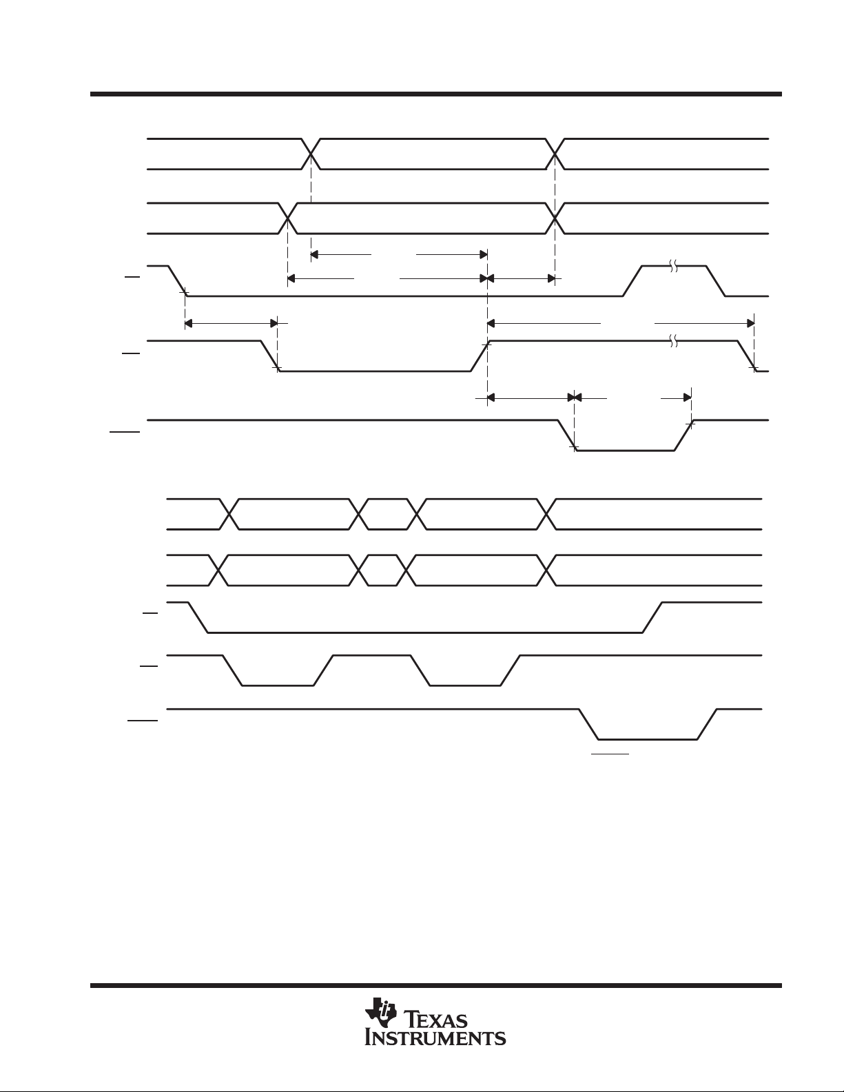
Setup time, CS low before negative WE edge 15 ns
Setup time, data ready before positive WE edge 10 ns
Setup time, addresses ready before positive WE edge 20 ns
Hold time, data and addresses held valid after positive WE edge 5 ns
Setup time, positive WE edge before LDAC low 5 ns
Pulse duration, WE high 20 ns
Pulse duration, LDAC low 23 ns
6
POST OFFICE BOX 655303 • DALLAS, TEXAS 75265
TLV5633C, TLV5633I
2.7 V TO 5.5 V LOW POWER 12-BIT DIGITAL-TO-ANALOG
CONVERTERS WITH INTERNAL REFERENCE AND POWER DOWN
SLAS190 – MARCH 1999
PARAMETER MEASUREMENT INFORMATION
D(0–7)
A(0,1)
CS
WE
LDAC
D(0–7)
X Data X
X Address X
t
su(D)
t
su(CS-WE)
t
su(A)
t
su(WE-LD)
t
h(DA)
t
wH(WE)
t
w(LD)
Figure 1. Timing Diagram
MSWX X LSW X
A(0,1)
CS
WE
LDAC
0XX1X
Figure 2. Example of a Complete Write Cycle (MSW, LSW) Using LDAC for Update
POST OFFICE BOX 655303 • DALLAS, TEXAS 75265
7

TLV5633C, TLV5633I
2.7 V TO 5.5 V LOW POWER 12-BIT DIGITAL-TO-ANALOG
CONVERTERS WITH INTERNAL REFERENCE AND POWER DOWN
SLAS190 – MARCH 1999
PARAMETER MEASUREMENT INFORMATION
D(0–7)
A(0,1)
CS
WE
LDAC
MSWX X LSW ControlXX
0XX13XX
Figure 3. Example of a Complete Write Cycle (MSW, LSW, Control)
8
POST OFFICE BOX 655303 • DALLAS, TEXAS 75265

TLV5633C, TLV5633I
2.7 V TO 5.5 V LOW POWER 12-BIT DIGITAL-TO-ANALOG
CONVERTERS WITH INTERNAL REFERENCE AND POWER DOWN
SLAS190 – MARCH 1999
TYPICAL CHARACTERISTICS
DIFFERENTIAL NONLINEARITY ERROR
1
0.8
0.6
0.4
0.2
0
–0.2
–0.4
–0.6
–0.8
–1
0 512 1024 1536 2048 2560
DNL – Differential Nonlinearity – LSB
Digital Code
Figure 4
INTEGRAL NONLINEARITY ERROR
3
3072 3584 4096
2
1
0
–1
–2
INL – Intergral Nonlinearity – LSB
–3
0 512 1024 1536 2048 2560
Digital Code
Figure 5
3072 3584 4096
POST OFFICE BOX 655303 • DALLAS, TEXAS 75265
9

TLV5633C, TLV5633I
2.7 V TO 5.5 V LOW POWER 12-BIT DIGITAL-TO-ANALOG
CONVERTERS WITH INTERNAL REFERENCE AND POWER DOWN
SLAS190 – MARCH 1999
TYPICAL CHARACTERISTICS
MAXIMUM OUTPUT VOLTAGE
LOAD CURRENT
2.04
2.0395
2.039
2.0385
2.038
2.0375
2.037
– Output Voltage – V
O
V
2.0365
2.036
2.0355
Slow Mode, Source
0 0.5 1 1.5 2 2.5 3
Fast Mode, Source
Load Current – mA
Figure 6
MINIMUM OUTPUT VOLTAGE
LOAD CURRENT
0.25
vs
AVDD = 3 V,
V
= Int. 1 V,
ref
Input Code = 0xFFF
vs
3.5 4 4.5
4.08
4.0795
4.079
4.0785
4.078
4.0775
4.077
– Output Voltage – V
O
V
4.0765
4.076
4.0755
0.25
MAXIMUM OUTPUT VOLTAGE
vs
LOAD CURRENT
AVDD = 5 V,
V
= Int. 2 V,
ref
Input Code = 0xFFF
Fast Mode, Source
Slow Mode, Source
0 0.5 1 1.5 2 2.5 3
Load Current – mA
Figure 7
MINIMUM OUTPUT VOLTAGE
vs
LOAD CURRENT
3.5 4 4.5
0.2
0.15
0.1
– Output Voltage – V
O
V
0.05
0
0 0.5 1 1.5 2 2.5 3
Load Current – mA
Figure 8
Fast Mode, Sink
Slow Mode, Sink
AVDD = 5 V,
V
= Int. 2 V,
ref
Input Code = 0x000
3.5 4 4.5
Fast Mode, Sink
0.2
0.15
0.1
– Output Voltage – V
O
V
0.05
0
0 0.5 1 1.5 2 2.5 3
Load Current – mA
Slow Mode, Sink
AVDD = 3 V,
V
= Int. 1 V,
ref
Input Code = 0x000
3.5 4 4.5
Figure 9
10
POST OFFICE BOX 655303 • DALLAS, TEXAS 75265

TLV5633C, TLV5633I
2.7 V TO 5.5 V LOW POWER 12-BIT DIGITAL-TO-ANALOG
CONVERTERS WITH INTERNAL REFERENCE AND POWER DOWN
SLAS190 – MARCH 1999
TYPICAL CHARACTERISTICS
TOTAL HARMONIC DISTORTION
FREQUENCY
0
AVDD = 5 V,
REF = 1 V dc + 1 V pp Sinewave,
–10
Output Full Scale
–20
–30
–40
–50
–60
–70
–80
THD – Total Harmonic Distortion – dB
–90
–100
100 1000
f – Frequency – Hz
Figure 10
vs
Slow Mode
Fast Mode
10000 100000
1
TOTAL HARMONIC DISTORTION AND NOISE
0
AVDD = 5 V,
REF = 1 V dc + 1 V pp Sinewave,
–10
Output Full Scale
–20
–30
–40
–50
–60
–70
–80
–90
–100
THD+N – Total Harmonic Distortion and Noise – dB
100 1000
POWER DOWN SUPPLY CURRENT
vs
TIME
vs
FREQUENCY
Slow Mode
Fast Mode
10000 100000
f – Frequency – Hz
Figure 11
0.9
0.8
0.7
0.6
0.5
0.4
– Supply Current – mA
0.3
DD
I
0.2
0.1
0
0102030405060
t – Time – µs
Figure 12
70 80 90
POST OFFICE BOX 655303 • DALLAS, TEXAS 75265
11

TLV5633C, TLV5633I
MODE
POWER
LATCH
2.7 V TO 5.5 V LOW POWER 12-BIT DIGITAL-TO-ANALOG
CONVERTERS WITH INTERNAL REFERENCE AND POWER DOWN
SLAS190 – MARCH 1999
APPLICATION INFORMATION
general function
The TLV5633 is a 12-bit, single supply DAC, based on a resistor string architecture. It consists of a parallel
interface, a speed and power down control logic, a programmable internal reference, a resistor string, and a
rail-to-rail output buffer. The output voltage (full scale determined by reference) is given by:
2REF
CODE
0 1000
[V]
Where REF is the reference voltage and CODE is the digital input value in the range 0x000 to 0xFFF. A power
on reset initially puts the internal latches to a defined state (all bits zero).
parallel interface
The device latches data on the positive edge of WE. It must be enabled with CS low. Whether the data is written
to one of the DAC holding latches (MSW, LSW) or the control register depends on the address bits A1 and A0.
LDAC
low updates the DAC with the value in the holding latch. LDAC is an asynchronous input and can be held
low, if a separate update is not necessary. However, to control the DAC using the load feature, there should be
approximately a 5 ns delay after the positive WE edge before driving LDAC low . Two more asynchronous inputs,
SPD and PWR control the settling times and the power-down mode:
SPD: Speed control 1 → fast mode 0 → slow mode
PWR: Power control 1 → normal operation 0 → power down
It is also possible to program the different modes (fast, slow , power down) and the DAC update latch using the
control register. The following tables list the possible combinations of control signals and control bits.
PIN BIT
SPD SPD
0 0 Slow
0 1 Fast
1 0 Fast
1 1 Fast
12
PIN BIT
PWR PWD
0 0 Down
0 1 Down
1 0 Normal
1 1 Down
PIN BIT
LDAC RLDAC
0 0 Transparent
0 1 Transparent
1 0 Hold
1 1 Transparent
POST OFFICE BOX 655303 • DALLAS, TEXAS 75265

TLV5633C, TLV5633I
2.7 V TO 5.5 V LOW POWER 12-BIT DIGITAL-TO-ANALOG
CONVERTERS WITH INTERNAL REFERENCE AND POWER DOWN
SLAS190 – MARCH 1999
APPLICATION INFORMATION
data format
The TLV5633 writes data either to one of the DAC holding latches or to the control register depending on the
address bits A1 and A0.
ADDRESS BITS
A1
0 0 DAC LSW holding
0 1 DAC MSW holding
1 0 Reserved
1 1 Control
The following table lists the meaning of the bits within the control register.
D7 D6 D5 D4 D3 D2 D1 D0
X X X REF1 REF0 RLDAC PWR SPD
†
X
†
Default values
X: don’t care
SPD: Speed control bit 1 → fast mode 0 → slow mode
PWR: Power control bit 1 → power down 0 → normal operation
RLDAC: Load DAC latch 1 → latch transparent 0 → DAC latch controlled by LDAC
†
X
†
X
A0 REGISTER
†
0
†
0
pin
†
0
†
0
†
0
REF1 and REF0 determine the reference source and the reference voltage.
REFERENCE BITS
REF1
REF0 REFERENCE
0 0 External
0 1 2.048 V
1 0 1.024 V
1 1 External
If an external reference voltage is applied to the REF pin, external reference must be selected.
layout considerations
T o achieve the best performance, it is recommended to have separate power planes for GND, A VDD, and DVDD.
Figure 13 shows how to lay out the power planes for the TL V5633. As a general rule, digital and analog signals
should be separated as wide as possible. To avoid crosstalk, analog and digital traces must not be routed in
parallel. The two positive power planes ( AV
ferrite bead.
A 100-nF ceramic low series inductance capacitor between DVDD and GND and a 1-µF tantalum capacitor
between AVDD and GND placed as close as possible to the supply pins are recommended for optimal
performance.
and DVDD) should be connected together at one point with a
DD
POST OFFICE BOX 655303 • DALLAS, TEXAS 75265
13

TLV5633C, TLV5633I
2.7 V TO 5.5 V LOW POWER 12-BIT DIGITAL-TO-ANALOG
CONVERTERS WITH INTERNAL REFERENCE AND POWER DOWN
SLAS190 – MARCH 1999
APPLICATION INFORMATION
layout considerations (continued)
DV
DD
AV
DD
Figure 13. TLV5633 Board Layout
linearity, offset, and gain error using single end supplies
When an amplifier is operated from a single supply , the voltage offset can still be either positive or negative. With
a positive offset, the output voltage changes on the first code change. With a negative offset the output voltage
may not change with the first code, depending on the magnitude of the offset voltage.
The output amplifier attempts to drive the output to a negative voltage. However, because the most negative
supply rail is ground, the output cannot drive below ground and clamps the output at 0 V.
The output voltage remains at zero until the input code value produces a sufficient positive output voltage to
overcome the negative offset voltage, resulting in the transfer function shown in Figure 14.
Output
Voltage
0 V
Negative
Offset
DAC Code
14
Figure 14. Effect of Negative Offset (Single Supply)
POST OFFICE BOX 655303 • DALLAS, TEXAS 75265

TLV5633C, TLV5633I
2.7 V TO 5.5 V LOW POWER 12-BIT DIGITAL-TO-ANALOG
CONVERTERS WITH INTERNAL REFERENCE AND POWER DOWN
SLAS190 – MARCH 1999
APPLICATION INFORMATION
The offset error , not the linearity error , produces this breakpoint. The transfer function would have followed the
dotted line if the output buffer could drive below the ground rail.
For a DAC, linearity is measured between zero input code (all inputs 0) and full scale code (all inputs 1) after
offset and full scale are adjusted out or accounted for in some way . However , single supply operation does not
allow for adjustment when the offset is negative due to the breakpoint in the transfer function. So the linearity
is measured between full scale code and the lowest code that produces a positive output voltage.
TLV5633 interfaced to an Intel MCS51 controller
The circuit in Figure 15 shows how to interface the TL V5633 to an Intel MCS51 microcontroller. The address
bus and the data bus of the controller are multiplexed on port 0 (non page mode) to save port pins. T o separate
the address bits and the data bits, the controller provides a dedicated signal, address latch enable (ALE), which
is connected to a latch at port 0.
An address decoder is required to generate the chip select signal for the TLV5633. In this example, a simple
3-to-8 decoder (74AC138) is used for the interface as shown in Figure 15. The DAC is memory mapped at
addresses 0x8000/1/2/3 within the data memory address space and mirrored every 32 address locations
(0x8020/1/2/3, 0x8040/1/2/3, etc.). In a typical microcontroller system, programmable logic should be used to
generate the chip select signals for the entire system.
The data pins and the WE
pin of the TL V5633 can be connected directly to the multiplexed address and data
bus and the WR signal of the controller.
The application uses the TL V5633 device’s internal reference at 2.048 V. The LDAC pin is connected to P3.5
and is used to update the DAC after both data bytes have been written.
8xC51
P2 A(15–8)
P0 AD(7–0)
ALE
WR
P3.5
8
8
D(7–0)
LE OE
8
74AC373
Q(7–0)
A2
A3
A4
DV
A15
DD
74AC138
Y(7–0)
A
B
C
G1
G2A
G2B
2
A(1–0)
D(7–0)
CS
WE
LDAC
8
8
TLV5633
G2A
16
SPD
PWR
OUT
DV
A(15–0)
AD(7–0)
CS(7–0)
DD
R
L
Figure 15. TLV5633 Interfaced to an Intel MCS51 Controller
MCS is a registered trademark of Intel Corporation.
To Other Devices Requiring
Voltage Reference
POST OFFICE BOX 655303 • DALLAS, TEXAS 75265
REF
15

TLV5633C, TLV5633I
2.7 V TO 5.5 V LOW POWER 12-BIT DIGITAL-TO-ANALOG
CONVERTERS WITH INTERNAL REFERENCE AND POWER DOWN
SLAS190 – MARCH 1999
APPLICATION INFORMATION
software
In the following example, the code generates a waveform at 20 KSPS with 32 samples stored in a table within
the program memory space of the microcontroller.
The waveform data is located in the program memory space at segment SINTBL beginning with the MSW of
the first 16-bit word (the 4 MSBs are ignored), followed by the LSW. T wo bytes are required for each DAC word
(the table is not shown in the code example).
The program consists of two parts:
D
A main routine, which is executed after reset and which initializes the timer and the interrupt system of the
microcontroller.
D
An interrupt service routine, which reads a new value from the waveform table and writes it to the DAC.
;––––––––––––––––––––––––––––––––––––––––––––––––––––––––––––––––––––––––––––––––––––––
; File: WAVE.A51
; Function: wave generation with TLV5633
; Processors: 80C51 family (running at 12MHz)
; Software: ASM51 assembler, Keil BL51 code–banking linker
; (C) 1999 Texas Instruments
;––––––––––––––––––––––––––––––––––––––––––––––––––––––––––––––––––––––––––––––––––––––
;––––––––––––––––––––––––––––––––––––––––––––––––––––––––––––––––––––––––––––––––––––––
; Program function declaration
;––––––––––––––––––––––––––––––––––––––––––––––––––––––––––––––––––––––––––––––––––––––
NAME WAVE
MAIN SEGMENT CODE
ISR SEGMENT CODE
WAVTBL SEGMENT CODE
VAR1 SEGMENT DATA
STACK SEGMENT IDATA
;––––––––––––––––––––––––––––––––––––––––––––––––––––––––––––––––––––––––––––––––––––––
; Code start at address 0, jump to start
;––––––––––––––––––––––––––––––––––––––––––––––––––––––––––––––––––––––––––––––––––––––
CSEG AT 0
LJMP start ; Execution starts at address 0 on power–up.
;––––––––––––––––––––––––––––––––––––––––––––––––––––––––––––––––––––––––––––––––––––––
; Code in the timer0 interrupt vector
;––––––––––––––––––––––––––––––––––––––––––––––––––––––––––––––––––––––––––––––––––––––
CSEG AT 0BH
LJMP timer0isr ; Jump vector for timer 0 interrupt is 000Bh
;––––––––––––––––––––––––––––––––––––––––––––––––––––––––––––––––––––––––––––––––––––––
; Define program variables
;––––––––––––––––––––––––––––––––––––––––––––––––––––––––––––––––––––––––––––––––––––––
RSEG VAR1
rolling_ptr: DS 1
16
POST OFFICE BOX 655303 • DALLAS, TEXAS 75265

TLV5633C, TLV5633I
2.7 V TO 5.5 V LOW POWER 12-BIT DIGITAL-TO-ANALOG
CONVERTERS WITH INTERNAL REFERENCE AND POWER DOWN
SLAS190 – MARCH 1999
APPLICATION INFORMATION
;––––––––––––––––––––––––––––––––––––––––––––––––––––––––––––––––––––––––––––––––––––––
; Interrupt service routine for timer 0 interrupts
;––––––––––––––––––––––––––––––––––––––––––––––––––––––––––––––––––––––––––––––––––––––
RSEG ISR
timer0isr:
PUSH PSW
PUSH ACC
; The signal to be output on the dac is stored in a table
; as 32 samples of msb, lsb pairs (64 bytes).
; The pointer, rolling_ptr, rolls round the table of samples
; incrementing by 2 bytes (1 sample) on each interrupt
; (at the end of this routine).
MOV DPTR, #wavetable ; set DPTR to the start of the table
MOV R0, #001H ; R0 selects DAC MSW
MOV A,rolling_ptr ; ACC loaded with the pointer into the wave table
MOVC A,@A+DPTR ; get msb from the table
MOVX @R0, A ; write DAC MSW
MOV R0, #000H ; R0 selects DAC LSW
MOV A,rolling_ptr ; move rolling pointer back in to ACC
INC A ; increment ACC holding the rolling pointer
MOVC A,@A+DPTR ; which is the lsb of this sample, now in ACC
MOVX @R0, A ; write DAC LSW
MOV A,rolling_ptr ; load ACC with rolling pointer again
INC A ; increment the ACC twice, to get next sample
INC A
ANL A,#003FH ; wrap back round to 0 if >64
MOV rolling_ptr,A ; move value held in ACC back to the rolling pointer
CLR T1 ; set LDACB = 0 (update DAC)
SETB T1 ; set LDACB = 1
POP ACC
POP PSW
RETI
;––––––––––––––––––––––––––––––––––––––––––––––––––––––––––––––––––––––––––––––––––––––
; Set up stack
;––––––––––––––––––––––––––––––––––––––––––––––––––––––––––––––––––––––––––––––––––––––
RSEG STACK
DS 10h ; 16 Byte Stack!
;––––––––––––––––––––––––––––––––––––––––––––––––––––––––––––––––––––––––––––––––––––––
; Main Program
;––––––––––––––––––––––––––––––––––––––––––––––––––––––––––––––––––––––––––––––––––––––
RSEG MAIN
start:
MOV SP,#STACK–1 ; first set Stack Pointer
CLR A
MOV rolling_ptr,A; set rolling pointer to 0
MOV TMOD,#002H ; set timer 0 to mode 2 – auto–reload
MOV TH0,#0CEH ; set timer 2 re–load value for 20 kHz interrupts
MOV P2, #080H ; set A15 of address bus high to ’memory map’
; device up beyond used address space
POST OFFICE BOX 655303 • DALLAS, TEXAS 75265
17

TLV5633C, TLV5633I
2.7 V TO 5.5 V LOW POWER 12-BIT DIGITAL-TO-ANALOG
CONVERTERS WITH INTERNAL REFERENCE AND POWER DOWN
SLAS190 – MARCH 1999
APPLICATION INFORMATION
SETB T1 ; set LDACB = 1 (on P3.5)
; TLV5633 setup
MOV R0, #003H ; R0 selects control register
MOV A, #011H ; LOAD ACC with control register value:
; REF1=1, REF0=0 –> 2.048V internal reference
; RLDAC=0 –> use LDACB pin to control DAC
; PD=0 –> DAC enabled
; SPD=1 –> FAST mode
; write control word:
MOVX @R0, A ; write DAC control word
SETB ET0 ; enable timer 0 interrupts
SETB EA ; enable all interrupts
SETB TR0 ; start timer 0
always:
SJMP always
RET
;––––––––––––––––––––––––––––––––––––––––––––––––––––––––––––––––––––––––––––––––––––––
; Table of 32 wave samples used as DAC data
;––––––––––––––––––––––––––––––––––––––––––––––––––––––––––––––––––––––––––––––––––––––
RSEG WAVTBL
wavetable:
;...insert 32 samples here...
.END
18
POST OFFICE BOX 655303 • DALLAS, TEXAS 75265

TLV5633C, TLV5633I
2.7 V TO 5.5 V LOW POWER 12-BIT DIGITAL-TO-ANALOG
CONVERTERS WITH INTERNAL REFERENCE AND POWER DOWN
SLAS190 – MARCH 1999
APPLICATION INFORMATION
definitions of specifications and terminology
integral nonlinearity (INL)
The relative accuracy or integral nonlinearity (INL), sometimes referred to as linearity error, is the maximum
deviation of the output from the line between zero and full scale excluding the effects of zero code and full-scale
errors.
differential nonlinearity (DNL)
The differential nonlinearity (DNL), sometimes referred to as differential error, is the difference between the
measured and ideal 1 LSB amplitude change of any two adjacent codes. Monotonic means the output voltage
changes in the same direction (or remains constant) as a change in the digital input code.
zero-scale error (E
Zero-scale error is defined as the deviation of the output from 0 V at a digital input value of 0.
gain error (EG)
Gain error is the error in slope of the DAC transfer function.
signal-to-noise ratio + distortion (SINAD)
Signal-to-noise ratio + distortion is the ratio of the rms value of the output signal to the rms sum of all other
spectral components below the Nyquist frequency , including harmonics but excluding dc. The value for SINAD
is expressed in decibels.
spurious free dynamic range (SFDR)
Spurious free dynamic range is the difference between the rms value of the output signal and the rms value of
the spurious signal within a specified bandwidth. The value for SFDR is expressed in decibels.
total harmonic distortion (THD)
T otal harmonic distortion is the ratio of the rms sum of the first six harmonic components to the rms value of the
fundamental signal and is expressed in decibels.
ZS
)
POST OFFICE BOX 655303 • DALLAS, TEXAS 75265
19

TLV5633C, TLV5633I
2.7 V TO 5.5 V LOW POWER 12-BIT DIGITAL-TO-ANALOG
CONVERTERS WITH INTERNAL REFERENCE AND POWER DOWN
SLAS190 – MARCH 1999
MECHANICAL DATA
DW (R-PDSO-G**) PLASTIC SMALL-OUTLINE PACKAGE
16 PIN SHOWN
0.050 (1,27)
16
1
0.020 (0,51)
0.014 (0,35)
9
0.299 (7,59)
0.293 (7,45)
8
A
0.010 (0,25)
0.419 (10,65)
0.400 (10,15)
M
0.010 (0,25) NOM
0°–8°
Gage Plane
0.010 (0,25)
0.050 (1,27)
0.016 (0,40)
0.104 (2,65) MAX
NOTES: A. All linear dimensions are in inches (millimeters).
B. This drawing is subject to change without notice.
C. Body dimensions do not include mold flash or protrusion not to exceed 0.006 (0,15).
D. Falls within JEDEC MS-013
0.012 (0,30)
0.004 (0,10)
PINS **
DIM
A MAX
A MIN
Seating Plane
0.004 (0,10)
16
0.410
(10,41)
0.400
(10,16)
20
0.510
(12,95)
0.500
(12,70)
24
0.610
(15,49)
0.600
(15,24)
4040000/D 02/98
20
POST OFFICE BOX 655303 • DALLAS, TEXAS 75265

TLV5633C, TLV5633I
2.7 V TO 5.5 V LOW POWER 12-BIT DIGITAL-TO-ANALOG
CONVERTERS WITH INTERNAL REFERENCE AND POWER DOWN
SLAS190 – MARCH 1999
MECHANICAL DATA
PW (R-PDSO-G**) PLASTIC SMALL-OUTLINE PACKAGE
14 PIN SHOWN
0,65
14
1
1,20 MAX
A
7
0,05 MIN
0,30
0,19
8
6,60
4,50
4,30
6,20
M
0,10
Seating Plane
0,10
0,15 NOM
Gage Plane
0,25
0°–8°
0,75
0,50
PINS **
DIM
A MAX
A MIN
NOTES: A. All linear dimensions are in millimeters.
B. This drawing is subject to change without notice.
C. Body dimensions do not include mold flash or protrusion not to exceed 0,15.
D. Falls within JEDEC MO-153
8
3,10
2,90
14
5,10
4,90
16
5,10
20
6,60
6,404,90
24
7,90
7,70
28
9,80
9,60
4040064/E 08/96
POST OFFICE BOX 655303 • DALLAS, TEXAS 75265
21

IMPORTANT NOTICE
T exas Instruments and its subsidiaries (TI) reserve the right to make changes to their products or to discontinue
any product or service without notice, and advise customers to obtain the latest version of relevant information
to verify, before placing orders, that information being relied on is current and complete. All products are sold
subject to the terms and conditions of sale supplied at the time of order acknowledgement, including those
pertaining to warranty, patent infringement, and limitation of liability.
TI warrants performance of its semiconductor products to the specifications applicable at the time of sale in
accordance with TI’s standard warranty. Testing and other quality control techniques are utilized to the extent
TI deems necessary to support this warranty . Specific testing of all parameters of each device is not necessarily
performed, except those mandated by government requirements.
CERTAIN APPLICA TIONS USING SEMICONDUCT OR PRODUCTS MAY INVOLVE POTENTIAL RISKS OF
DEATH, PERSONAL INJURY, OR SEVERE PROPERTY OR ENVIRONMENTAL DAMAGE (“CRITICAL
APPLICATIONS”). TI SEMICONDUCTOR PRODUCTS ARE NOT DESIGNED, AUTHORIZED, OR
WARRANTED TO BE SUITABLE FOR USE IN LIFE-SUPPORT DEVICES OR SYSTEMS OR OTHER
CRITICAL APPLICA TIONS. INCLUSION OF TI PRODUCTS IN SUCH APPLICATIONS IS UNDERST OOD TO
BE FULLY AT THE CUSTOMER’S RISK.
In order to minimize risks associated with the customer’s applications, adequate design and operating
safeguards must be provided by the customer to minimize inherent or procedural hazards.
TI assumes no liability for applications assistance or customer product design. TI does not warrant or represent
that any license, either express or implied, is granted under any patent right, copyright, mask work right, or other
intellectual property right of TI covering or relating to any combination, machine, or process in which such
semiconductor products or services might be or are used. TI’s publication of information regarding any third
party’s products or services does not constitute TI’s approval, warranty or endorsement thereof.
Copyright 1999, Texas Instruments Incorporated
 Loading...