

Datasheet TLV5619QDWR, TLV5619QDW, TLV5619IPWR, TLV5619IPW, TLV5619IDWR Datasheet (Texas Instruments)
...
TLV5619
2.7 V TO 5.5 V 12-BIT PARALLEL DIGITAL-TO-ANALOG CONVERTER
WITH POWER DOWN
SLAS172C – DECEMBER 1997 – REVISED APRIL 2000
1
POST OFFICE BOX 655303 • DALLAS, TEXAS 75265
D
Single Supply 2.7-V to 5.5-V Operation
D
±0.4 LSB Differential Nonlinearity (DNL),
±1.5 LSB Integral Nonlinearity (INL)
D
12-Bit Parallel Interface
D
Compatible With TMS320 DSP
D
Internal Power On Reset
D
Settling Time 1 µs Typ
D
Low Power Consumption:
– 8 mW for 5-V Supply
– 4.3 mW for 3-V Supply
D
Reference Input Buffers
D
Voltage Output
D
Monotonic Over Temperature
D
Asynchronous Update
applications
D
Battery Powered Test Instruments
D
Digital Offset and Gain Adjustment
D
Battery Operated/Remote Industrial
Controls
D
Machine and Motion Control Devices
D
Cordless and Wireless Telephones
D
Speech Synthesis
D
Communication Modulators
D
Arbitrary Waveform Generation
description
The TL V5619 is a 12-bit voltage output DAC with
a microprocessor and TMS320 compatible
parallel interface. The 12 data bits are double
buffered so that the output can be updated
asynchronously using the LDAC
pin. During
normal operation, the device dissipates 8 mW at
a 5-V supply and 4.3 mW at a 3-V supply. The
power consumption can be lowered to 50 nW by
setting the DAC to power-down mode.
The output voltage is buffered by a ×2 gain
rail-to-rail amplifier, which features a Class A
output stage to improve stability and reduce
settling time.
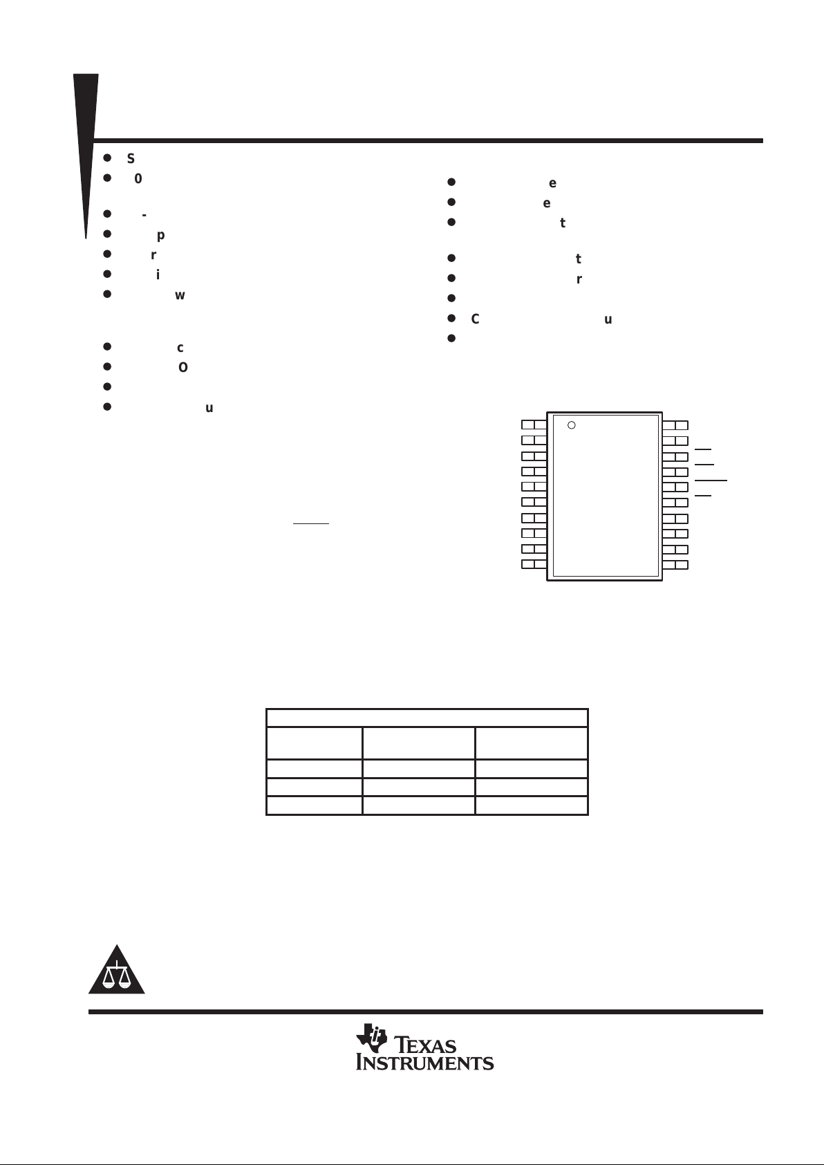
AVAILABLE OPTIONS
PACKAGE
T
A
SMALL OUTLINE
(DW)
TSSOP
(PW)
0°C to 70°C TLV5619CDW TLV5619CPW
–40°C to 85°C TLV5619IDW TLV5619IPW
–40°C to 125°C TLV5619QDW —
Please be aware that an important notice concerning availability, standard warranty, and use in critical applications of
Texas Instruments semiconductor products and disclaimers thereto appears at the end of this data sheet.
Copyright 2000, Texas Instruments Incorporated
PRODUCTION DATA information is current as of publication date.
Products conform to specifications per the terms of Texas Instruments
standard warranty. Production processing does not necessarily include
testing of all parameters.
1
2
3
4
5
6
7
8
9
10
20
19
18
17
16
15
14
13
12
11
D2
D3
D4
D5
D6
D7
D8
D9
D10
D11
D1
D0
CS
WE
LDAC
PD
GND
OUT
REFIN
V
DD
DW OR PW PACKAGE
(TOP VIEW)
TLV5619
2.7 V TO 5.5 V 12-BIT PARALLEL DIGITAL-TO-ANALOG CONVERTER
WITH POWER DOWN
SLAS172C – DECEMBER 1997 – REVISED APRIL 2000
2
POST OFFICE BOX 655303 • DALLAS, TEXAS 75265
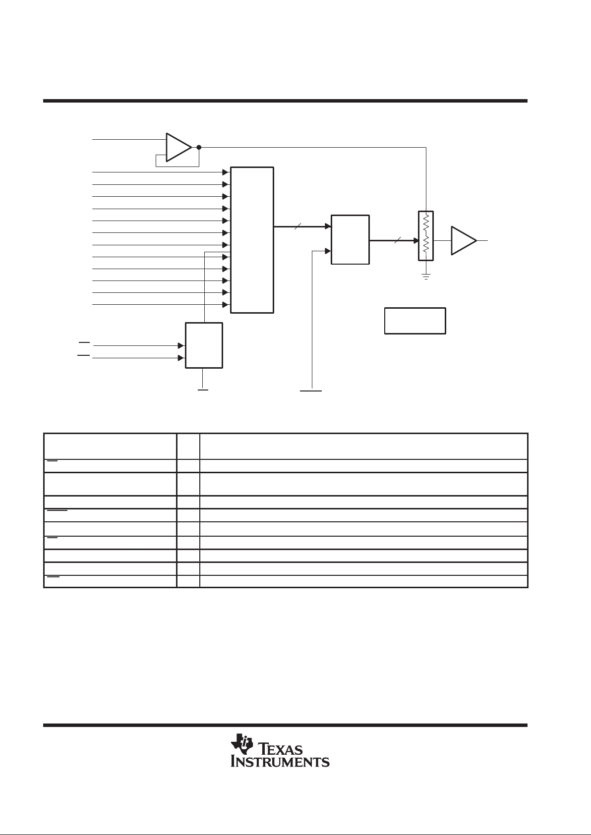
functional block diagram
_
+
REFIN
12
19
20
1
2
3
4
5
6
18
17
D0
D1
D2
D3
D4
D5
D6
D7
CS
WE
Power-On
Reset
12
12
x2
LDAC
16
13
OUT
12-Bit
Input
Register
Select
and
Control
Logic
12-Bit
DAC
Latch
7
D8
8
D9
9
D10
10
D11
PD
15
Resistor
String DAC
Terminal Functions
TERMINAL
NAME NO.
I/O
DESCRIPTION
CS 18 I Chip select
D0 (LSB)–D11 (MSB)
19, 20,
1 – 10
I Parallel data input
GND 14 Ground
LDAC 16 I Load DAC
OUT 13 O Analog output
PD 15 I When low, disables all buffer amplifier voltages to reduce supply current
REFIN 12 I Voltage reference input
V
DD
11 Positive power supply
WE 17 I Write enable
TLV5619
2.7 V TO 5.5 V 12-BIT PARALLEL DIGITAL-TO-ANALOG CONVERTER
WITH POWER DOWN
SLAS172C – DECEMBER 1997 – REVISED APRIL 2000
3
POST OFFICE BOX 655303 • DALLAS, TEXAS 75265
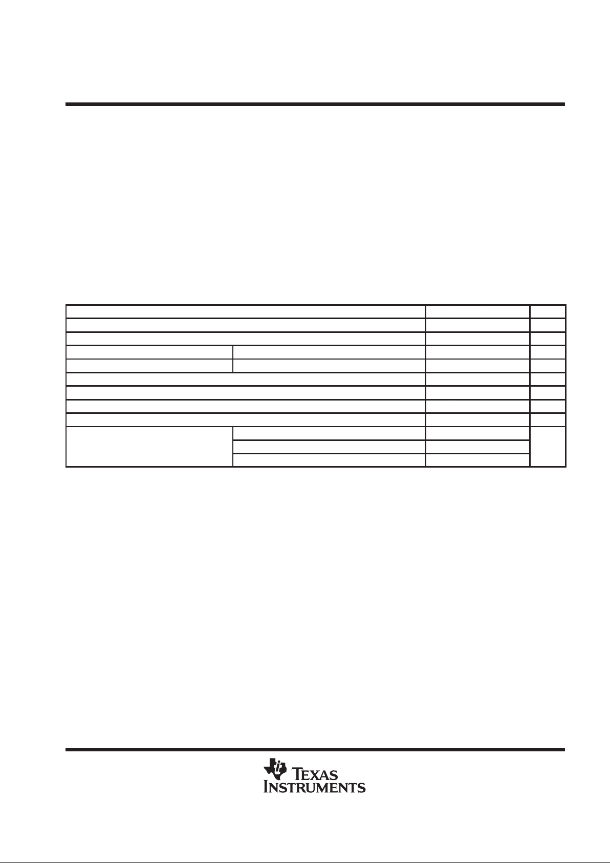
absolute maximum ratings over operating free-air temperature range (unless otherwise noted)
†
Supply voltage (VDD to GND) 7 V. . . . . . . . . . . . . . . . . . . . . . . . . . . . . . . . . . . . . . . . . . . . . . . . . . . . . . . . . . . . . . . .
Analog input voltage range – 0.3 V to VDD + 0.3 V. . . . . . . . . . . . . . . . . . . . . . . . . . . . . . . . . . . . . . . . . . . . . . . . . .
Reference input voltage V
DD
+ 0.3 V. . . . . . . . . . . . . . . . . . . . . . . . . . . . . . . . . . . . . . . . . . . . . . . . . . . . . . . . . . . . .
Digital input voltage range to GND – 0.3 V to VDD + 0.3 V. . . . . . . . . . . . . . . . . . . . . . . . . . . . . . . . . . . . . . . . . . .
Operating free-air temperature range, TA: TLV5619C 0°C to 70°C. . . . . . . . . . . . . . . . . . . . . . . . . . . . . . . . . . . .
TLV5619I –40°C to 85°C. . . . . . . . . . . . . . . . . . . . . . . . . . . . . . . . . . .
TLV5619Q –40°C to 125°C. . . . . . . . . . . . . . . . . . . . . . . . . . . . . . . . .
Storage temperature range, T
stg
–65°C to 150°C. . . . . . . . . . . . . . . . . . . . . . . . . . . . . . . . . . . . . . . . . . . . . . . . . . .
Lead temperature 1,6 mm (1/16 inch) from case for 10 seconds 260°C. . . . . . . . . . . . . . . . . . . . . . . . . . . . . . .
†
Stresses beyond those listed under “absolute maximum ratings” may cause permanent damage to the device. These are stress ratings only, and
functional operation of the device at these or any other conditions beyond those indicated under “recommended operating conditions” is not
implied. Exposure to absolute-maximum-rated conditions for extended periods may affect device reliability.
recommended operating conditions
MIN NOM MAX UNIT
Supply voltage, VDD (5-V Supply) 4.5 5 5.5 V
Supply voltage, VDD (3-V Supply) 2.7 3 3.3 V
High-level digital input voltage, V
IH
V
DD
2 V
Low-level digital input voltage, V
IL
V
DD
0.8 V
Reference voltage, V
ref
to REFIN terminal (5-V Supply) 0 2.048 VDD–1.5 V
Reference voltage, V
ref
to REFIN terminal (3-V Supply) 0 1.024 VDD–1.5 V
Load resistance, R
L
2 10 kΩ
Load capacitance, C
L
100 pF
TLV5619C 0 70
Operating free-air temperature, T
A
TLV5619I –40 85
°C
TLV5619Q –40 125
NOTES: 1. The recommended operating levels for both VIH and VIL apply to all valid values of VDD.
2. Reference input voltages greater than VDD/2 will cause output saturation for large DAC codes.
TLV5619
2.7 V TO 5.5 V 12-BIT PARALLEL DIGITAL-TO-ANALOG CONVERTER
WITH POWER DOWN
SLAS172C – DECEMBER 1997 – REVISED APRIL 2000
4
POST OFFICE BOX 655303 • DALLAS, TEXAS 75265
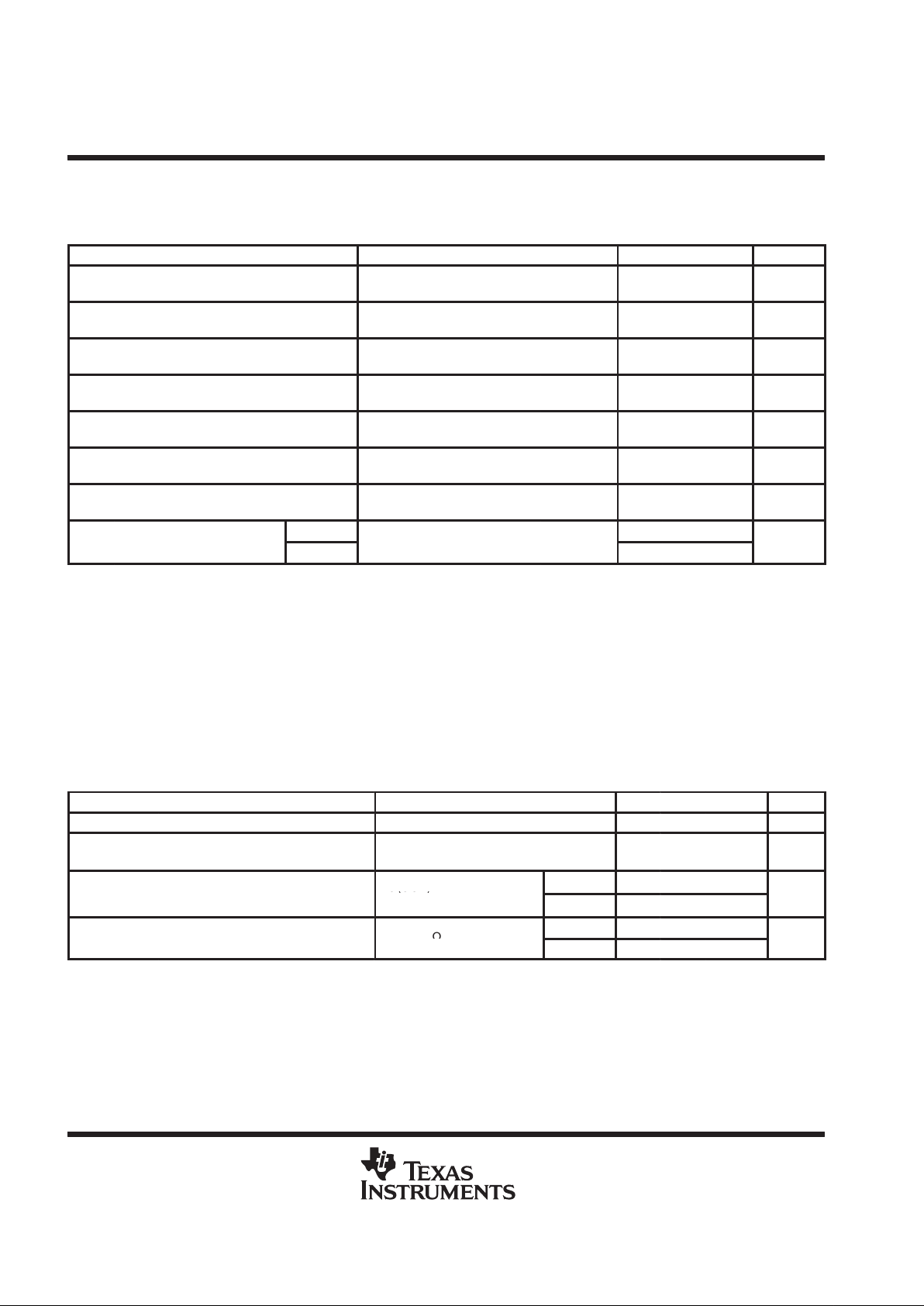
electrical characteristics over recommended operating free-air temperature range, supply
voltages, and reference voltages (unless otherwise noted)
static DAC specifications
PARAMETER TEST CONDITIONS MIN TYP MAX UNIT
Resolution
V
ref(REFIN)
= 2.048 V at 5 V ,
1.024 V at 3 V
12 bits
Integral nonlinearity (INL)
V
ref(REFIN)
= 2.048 V at 5 V ,
1.024 V at 3 V ,
See Note 3 ±1.5 ±4 LSB
Differential nonlinearity (DNL)
V
ref(REFIN)
= 2.048 V at 5 V ,
1.024 V at 3 V ,
See Note 4 ± 0.4 ± 1 LSB
E
ZS
Zero-scale error (offset error at zero scale)
V
ref(REFIN)
= 2.048 V at 5 V ,
1.024 V at 3 V ,
See Note 5 ±3 ±20 mV
Zero-scale-error temperature coefficient
V
ref(REFIN)
= 2.048 V at 5 V ,
1.024 V at 3 V ,
See Note 6 3 ppm/°C
E
G
Gain error
V
ref(REFIN)
= 2.048 V at 5 V ,
1.024 V at 3 V ,
See Note 7 ±0.25 ±0.5
% of FS
voltage
Gain error temperature coefficient
V
ref(REFIN)
= 2.048 V at 5 V ,
1.024 V at 3 V ,
See Note 8 1 ppm/°C
pp
Zero scale
65
PSRR
Power-supply rejection ratio
Gain
See Notes 9 and 10
65
dB
NOTES: 3. The relative accuracy or integral nonlinearity (INL), sometimes referred to as linearity error, is the maximum deviation of the output
from the line between zero and full scale excluding the effects of zero code and full-scale errors.
4. The differential nonlinearity (DNL), sometimes referred to as differential error, is the difference between the measured and ideal 1
LSB amplitude change of any two adjacent codes. Monotonic means the output voltage changes in the same direction (or remains
constant) as a change in the digital input code.
5. Zero-scale error is the deviation from zero voltage output when the digital input code is zero.
6. Zero-scale-error temperature coefficient is given by: EZSTC = [EZS(T
max
) – EZS(T
min
)]/V
ref
× 106/(T
max
– T
min
).
7. Gain error is the deviation from the ideal output (2 × V
ref
– 1 LSB) with an output load of 10 kΩ excluding the effects of the zero-error.
8. Gain temperature coefficient is given by: EGTC = [EG(T
max
) – EG (T
min
)]/V
ref
× 106/(T
max
– T
min
).
9. Zero-scale-error rejection ratio (EZS-RR) is measured by varying the VDD from 4.5 V to 5.5 V dc and measuring the proportion of
this signal imposed on the zero-code output voltage.
10. Gain-error rejection ratio (EG-RR) is measured by varying the VDD from 4.5 V to 5.5 V dc and measuring the proportion of this signal
imposed on the full-scale output voltage after subtracting the zero scale change.
output specifications
PARAMETER TEST CONDITIONS MIN TYP MAX UNIT
V
O
Voltage output range RL = 10 kΩ 0 VDD–0.4 V
Output load regulation accuracy
V
O(OUT)
= 4.096 V,
2.048 V
RL = 2 kΩ 0.1 0.29
% of FS
voltage
p
V
O(OUT
)
= 0 V,
5-V Supply 100
I
OSC(
source
)
Out ut short circuit source current
O(OUT)
Full scale code
3-V Supply 25
mA
p
5-V Supply 10
I
O(
source
)
Out ut source current
R
L
=
100 Ω
3-V Supply 10
mA
TLV5619
2.7 V TO 5.5 V 12-BIT PARALLEL DIGITAL-TO-ANALOG CONVERTER
WITH POWER DOWN
SLAS172C – DECEMBER 1997 – REVISED APRIL 2000
5
POST OFFICE BOX 655303 • DALLAS, TEXAS 75265
electrical characteristics over recommended operating free-air temperature range, supply
voltages, and reference voltages (unless otherwise noted)
reference input (REFIN)
PARAMETER TEST CONDITIONS MIN TYP MAX UNIT
V
ref
Reference input voltage See Note 11 0 VDD–1.5 V
RiReference input resistance 10 MΩ
CiReference input capacitance 5 pF
Reference feed through REFIN = 1 Vpp at 1 kHz + 1.024 V dc (see Note 12) –60 dB
Reference input bandwidth REFIN = 0.2 Vpp + 1.024 V dc at –3 dB 1.4 MHz
NOTES: 11. Reference input voltages greater than VDD/2 will cause output saturation for large DAC codes.
12. Reference feedthrough is measured at the DAC output with an input code = 0x000 and a V
ref(REFIN)
input = 1.024 V dc + 1 Vpp at
1 kHz.
digital inputs (D0 – D11, CS, WE, LDAC, PD)
PARAMETER TEST CONDITIONS MIN TYP MAX UNIT
I
IH
High-level digital input current VI = V
DD
1 µA
I
IL
Low-level digital input current VI = 0 V –1 µA
C
i
Input capacitance 8 pF
power supply
PARAMETER TEST CONDITIONS MIN TYP MAX
UNIT
pp
p
5-V Supply 1.6 3
IDDPower supply current
No load
,
All inputs 0 V or V
DD
3-V Supply 1.44 2.7
mA
Power down supply current 0.01 10 µA
TLV5619
2.7 V TO 5.5 V 12-BIT PARALLEL DIGITAL-TO-ANALOG CONVERTER
WITH POWER DOWN
SLAS172C – DECEMBER 1997 – REVISED APRIL 2000
6
POST OFFICE BOX 655303 • DALLAS, TEXAS 75265
operating characteristics over recommended operating free-air temperature range, supply
voltages, and reference voltages (unless otherwise noted)
analog output dynamic performance
PARAMETER TEST CONDITIONS MIN TYP MAX UNIT
CL = 100 pF,
R
= 10 kΩ,
V
ref(REFIN)
= 2.048 V,
1.024 V,
5-V
Supply
8 12 V/µs
SR
Slew rate
L
,
Code 32 to code 4095,
Code 4095 to code 32,
,
VO from 10% to 90%
90% to 10%
3-V
Supply
6 9 V/µs
t
s
Output settling time (full scale)
To ±0.5 LSB,
RL = 10 kΩ,
CL = 100 pF,
See Note 13
1 3 µs
Glitch energy DIN = all 0s to all 1s 5 nV–s
S/N Signal to noise
fs = 480 kSPS,
BW = 20 kHz,
CL = 100 pF,
f
OUT
= 1 kHz,
RL = 10 kΩ
TA = 25°C, See Note 14
5-V
Supply
65 78
fs = 480 kSPS,
f
OUT
= 1 kHz,
5-V
Supply
58 67
S/(N+D)
Signal to noise + distortion
BW
= 20
kHz
,
CL = 100 pF,
R
L
= 10 kΩ,
TA = 25°C, See Note 14
3-V
Supply
58 69
dB
Total harmonic distortion
fs = 480 kSPS,
BW = 20 kHz,
CL = 100 pF,
f
OUT
= 1 kHz,
RL = 10 kΩ,
TA = 25°C, See Note 14
–68 –60
Spurious free dynamic range
fs = 480 kSPS,
BW = 20 kHz,
CL = 100 pF,
f
OUT
= 1 kHz,
RL = 10 kΩ,
TA = 25°C, See Note 14
60 72
NOTES: 13. Settling time is the time for the output signal to remain within ±0.5 LSB of the final measured value for a digital input code change
of 0x020 to 0x3DF or 0x3DF to 0x020. Limits are ensured by design and characterization, but are not production tested.
14. 1 kHz sinewave generated by DAC, reference voltage = 1.024 V at 3 V and 2.048 V at 5 V.

TLV5619
2.7 V TO 5.5 V 12-BIT PARALLEL DIGITAL-TO-ANALOG CONVERTER
WITH POWER DOWN
SLAS172C – DECEMBER 1997 – REVISED APRIL 2000
7
POST OFFICE BOX 655303 • DALLAS, TEXAS 75265
timing requirement
digital inputs
MIN NOM MAX UNIT
t
su(CS-WE)
Setup time, CS low before negative WE edge 13 ns
t
su(D)
Setup time, data ready before positive WE edge 9 ns
t
h(D)
Hold time, data held after positive WE edge 0 ns
t
su(WE-LD)
Setup time, positive WE edge before LDAC low 0 ns
t
wh(WE)
Pulse width, WE high 10 ns
t
w(LD)
Pulse width, LDAC low 10 ns
PARAMETER MEASUREMENT INFORMATION
X Data X
t
su(D)
t
h(D)
t
su(CE-WE)
t
wh(WE)
t
su(WE-LD)
t
w(LD)
D(0–11)
CS
WE
LDAC
Figure 1. Timing Diagram

TLV5619
2.7 V TO 5.5 V 12-BIT PARALLEL DIGITAL-TO-ANALOG CONVERTER
WITH POWER DOWN
SLAS172C – DECEMBER 1997 – REVISED APRIL 2000
8
POST OFFICE BOX 655303 • DALLAS, TEXAS 75265
TYPICAL CHARACTERISTICS
Figure 2
3
2
1
100 k 10 k 1 k
– Output Voltage – V
4
MAXIMUM OUTPUT VOLTAGE
vs
LOAD
5
100 10
VDD = 5 V, V
ref
= 2 V,
Input Code = 4095
RL – Output Load – Ω
V
O
Figure 3
2
1.5
1
0.5
100 k 10 k 1 k
– Output Voltage – V
2.5
MAXIMUM OUTPUT VOLTAGE
vs
LOAD
3
100 10
VDD = 3 V, V
ref
= 1.2 V,
Input Code = 4095
RL – Output Load – Ω
V
O
Figure 4
–60
–80
–100
THD – Total Harmonic Distortion – dB
–40
–20
TOTAL HARMONIC DISTORTION
vs
LOAD
0
100 k 10 k 1 k 100 10
VDD = 5 V, V
ref
= 2 V,
Tone at 1 kHz
RL – Output Load – Ω
Figure 5
–30
–50
–70
–80
0 5 10 15 20
–20
–10
f – Frequency – kHz
0
25 30 35
TOTAL HARMONIC DISTORTION
vs
FREQUENCY
–40
–60
THD – Total Harmonic Distortion – dB
VDD = 5 V
TLV5619
2.7 V TO 5.5 V 12-BIT PARALLEL DIGITAL-TO-ANALOG CONVERTER
WITH POWER DOWN
SLAS172C – DECEMBER 1997 – REVISED APRIL 2000
9
POST OFFICE BOX 655303 • DALLAS, TEXAS 75265
TYPICAL CHARACTERISTICS
Figure 6
40
30
10
0
0 5 10 15 20
SNRD – Signal-To-Noise Ratio + Distortion – dB
50
70
f – Frequency – kHz
SIGNAL-TO-NOISE + DISTORTION
vs
FREQUENCY
80
25 30 35
60
20
VDD = 5 V
1
0.8
0.6
0.4
0.2
0
–0.2
–0.4
–0.6
–0.8
–1
DNL – Differential Nonlinearity – LSB
0 500 1000 1500 2000 2500 3000 3500 4000
Code
Figure 7. Differential Nonlinearity

TLV5619
2.7 V TO 5.5 V 12-BIT PARALLEL DIGITAL-TO-ANALOG CONVERTER
WITH POWER DOWN
SLAS172C – DECEMBER 1997 – REVISED APRIL 2000
10
POST OFFICE BOX 655303 • DALLAS, TEXAS 75265
TYPICAL CHARACTERISTICS
2
1.5
1
0.5
0
–0.5
–1
–1.5
–2
0 500 1000 1500 2000 2500 3000 3500 4000
Code
INL – Integral Nonlinearity – LSB
3
4
–3
–4
Figure 8. Integral Nonlinearity
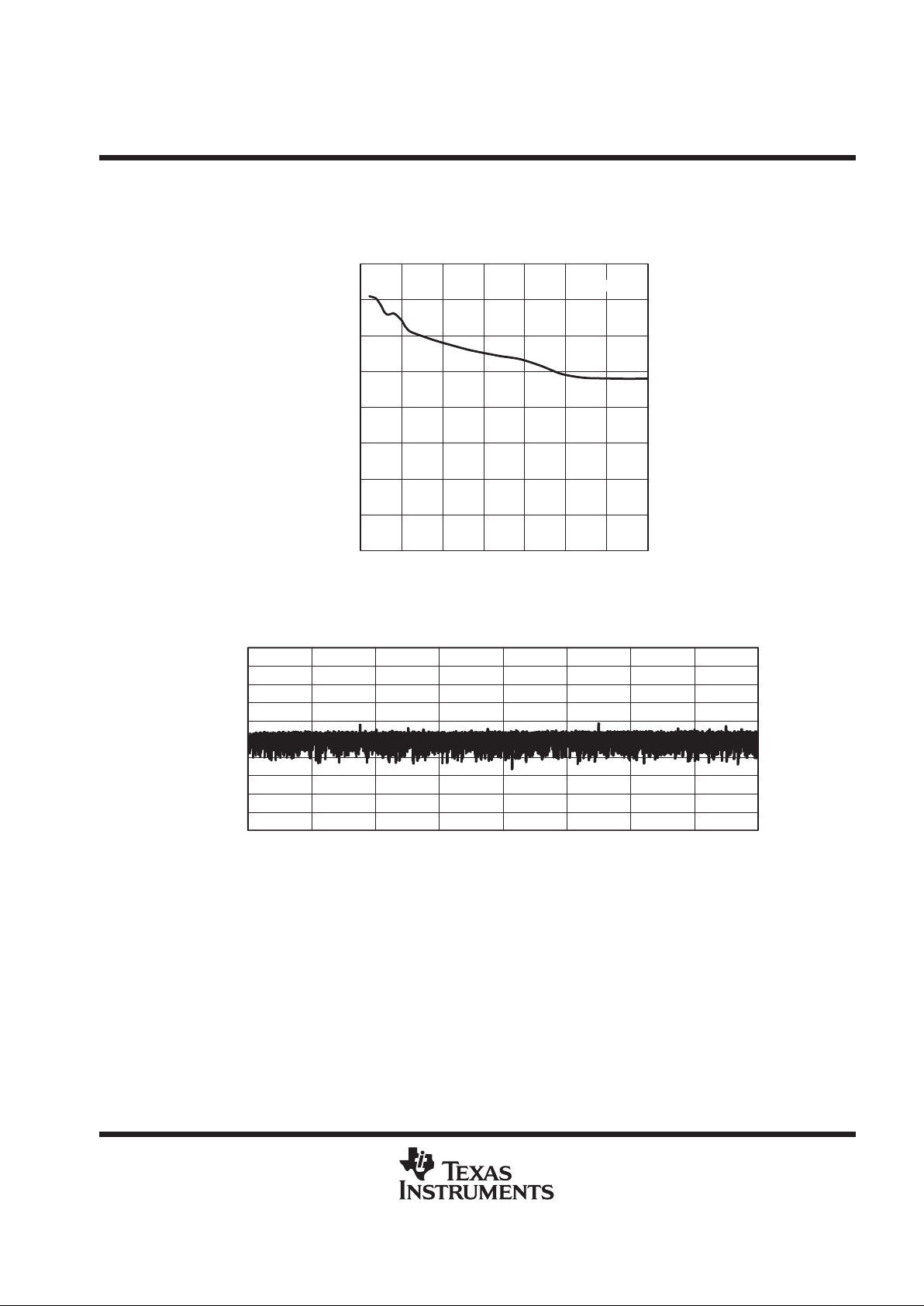
POWER DOWN SUPPLY CURRENT
vs
TIME
0.00001
0.000001
100 300
t – Time – ms
0.01
0.001
0.0001
200 400 5000
0.1
1
600
I
DD
– Supply Current – mA
Figure 9

TLV5619
2.7 V TO 5.5 V 12-BIT PARALLEL DIGITAL-TO-ANALOG CONVERTER
WITH POWER DOWN
SLAS172C – DECEMBER 1997 – REVISED APRIL 2000
11
POST OFFICE BOX 655303 • DALLAS, TEXAS 75265
APPLICATION INFORMATION
definitions of specifications and terminology
integral nonlinearity (INL)
The relative accuracy or integral nonlinearity (INL), sometimes referred to as linearity error, is the maximum
deviation of the output from the line between zero and full scale excluding the effects of zero code and full-scale
errors.
differential nonlinearity (DNL)
The differential nonlinearity (DNL), sometimes referred to as differential error, is the difference between the
measured and ideal 1 LSB amplitude change of any two adjacent codes. Monotonic means the output voltage
changes in the same direction (or remains constant) as a change in the digital input code.
zero-scale error (E
ZS
)
Zero-scale error is defined as the deviation of the output from 0 V at a digital input value of 0.
gain error (E
G
)
Gain error is the error in slope of the DAC transfer function.
signal-to-noise ratio + distortion (S/N+D)
S/N+D is the ratio of the rms value of the output signal to the rms sum of all other spectral components below
the Nyquist frequency, including harmonics but excluding dc. The value for S/N+D is expressed in decibels.
spurious free dynamic range (SFDR)
SFDR is the difference between the rms value of the output signal and the rms value of the largest spurious
signal within a specified bandwidth. The value for SFDR is expressed in decibels.
total harmonic distortion (THD)
THD is the ratio of the rms sum of the first six harmonic components to the rms value of the fundamental signal
and is expressed in decibels.
TLV5619
2.7 V TO 5.5 V 12-BIT PARALLEL DIGITAL-TO-ANALOG CONVERTER
WITH POWER DOWN
SLAS172C – DECEMBER 1997 – REVISED APRIL 2000
12
POST OFFICE BOX 655303 • DALLAS, TEXAS 75265
APPLICATION INFORMATION
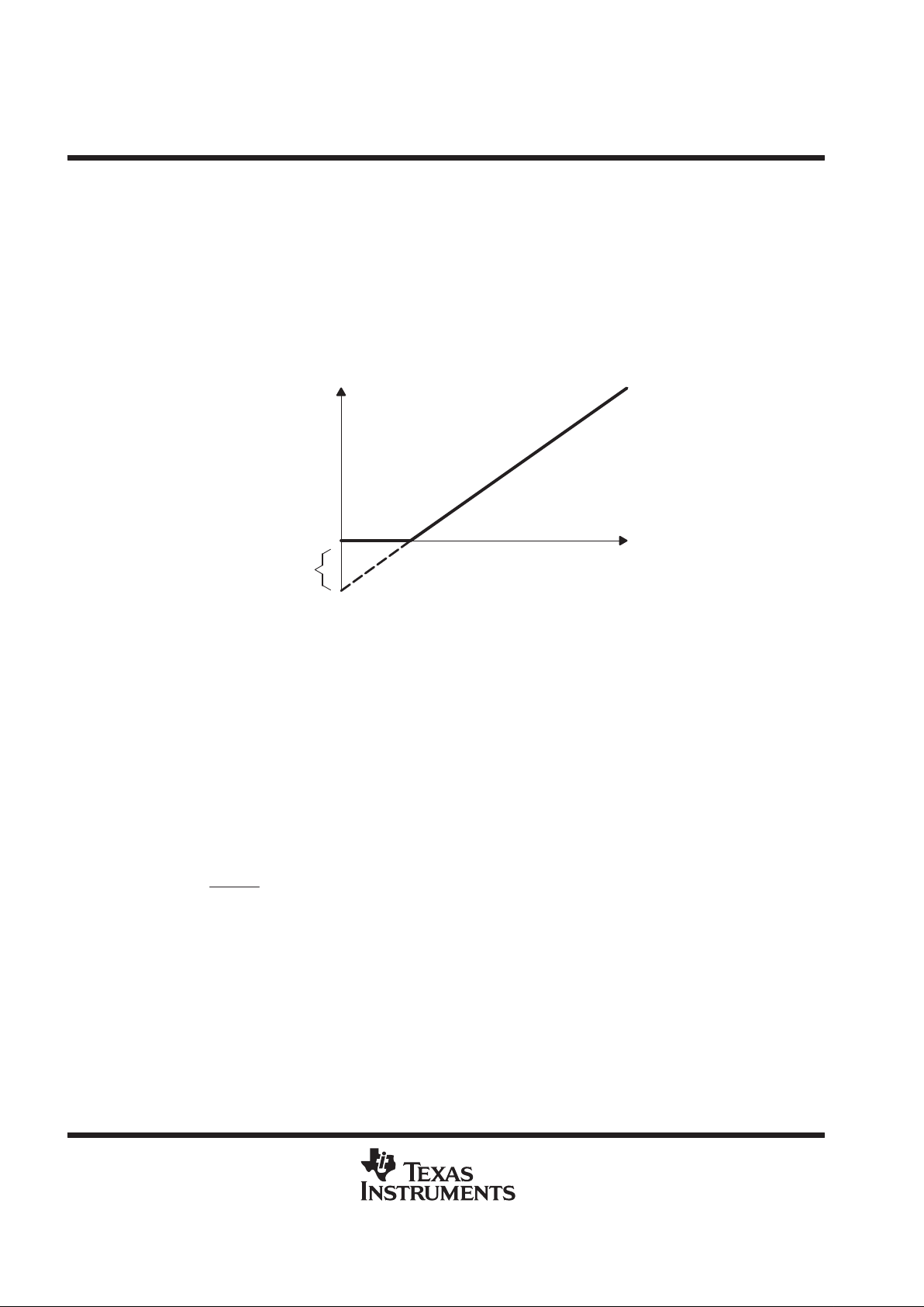
linearity, offset, and gain error using single end supplies
When an amplifier is operated from a single supply , the voltage offset can still be either positive or negative. With
a positive offset, the output voltage changes on the first code change. With a negative offset the output voltage
may not change with the first code depending on the magnitude of the offset voltage.
The output amplifier attempts to drive the output to a negative voltage. However, because the most negative
supply rail is ground, the output cannot drive below ground and clamps the output at 0 V.
The output voltage remains at zero until the input code value produces a sufficient positive output voltage to
overcome the negative offset voltage, resulting in the transfer function shown in Figure 10.
DAC Code
Output
Voltage
0 V
Negative
Offset
Figure 10. Effect of Negative Offset (Single Supply)
This offset error, not the linearity error , produces this breakpoint. The transfer function would have followed the
dotted line if the output buffer could drive below the ground rail.
For a DAC, linearity is measured between zero input code (all inputs 0) and full scale code (all inputs 1) after
offset and full scale are adjusted out or accounted for in some way . However , single supply operation does not
allow for adjustment when the offset is negative due to the breakpoint in the transfer function. So the linearity
is measured between full scale code and the lowest code that produces a positive output voltage.
general function
The TLV5619 is a 12-bit, single supply DAC, based on a resistor string architecture. It consists of a parallel
interface, a power down control logic, a resistor string, and a rail-to-rail output buffer. The output voltage (full
scale determined by reference) is given by:
2REF
CODE
0x1000
[V]
Where REF is the reference voltage and CODE is the digital input value, range 0x000 to 0xFFF. A power on
reset initially puts the internal latches to a defined state (all bits zero).

TLV5619
2.7 V TO 5.5 V 12-BIT PARALLEL DIGITAL-TO-ANALOG CONVERTER
WITH POWER DOWN
SLAS172C – DECEMBER 1997 – REVISED APRIL 2000
13
POST OFFICE BOX 655303 • DALLAS, TEXAS 75265
APPLICATION INFORMATION
parallel interface
The device latches data on the positive edge of WE. It must be enabled with CS low. LDAC low updates the
DAC with the value in the holding latch. LDAC is an asynchronous input and can be held low, if a separate update
is not necessary . However, to control the DAC using the load feature, LDAC can be driven low after the positive
WE edge.
Address
Decoder
A(0–15)
IS
WE
D(0–15)
CS
LDAC
WE
D(0–11)
TMS320C2XX, 5X
TLV5619
Figure 11. Proposed Interface Between TLV5619 and TMS320C2XX, 5X DSPs
Address
Decoder
A(0–15)
TCLK0
R/W
D(0–15)
CS
LDAC
WE
D(0–11)
TMS320C3X
TLV5619
IOSTROBE
Figure 12. Proposed Interface Between TLV5619 and TMS320C3X DSPs

TLV5619
2.7 V TO 5.5 V 12-BIT PARALLEL DIGITAL-TO-ANALOG CONVERTER
WITH POWER DOWN
SLAS172C – DECEMBER 1997 – REVISED APRIL 2000
14
POST OFFICE BOX 655303 • DALLAS, TEXAS 75265
APPLICATION INFORMATION
TLV5619 interfaced to TMS320C203 DSP
hardware interface
Figure 13 shows an example of the connection between the TLV5619 and the TMS320C203 DSP. The only
other device that is needed in addition to the DSP and the DAC is the 74AC138 address decoding circuit . Using
this configuration, the DAC address is 0x0084 within the I/O memory space of the TMS320C203.
LDAC
is held low so that the output voltage is updated with the rising WE edge. The power down mode is
deactivated permanently by pulling PD
to VDD.
A2
A3
A4
A6
IS
D(0–11)
5 V
A
B
C
G1
G2A
G2B
CS
D(0–11)
Y1
V
DD
PD
WE
REFIN
Output
REF191
OUT
LDAC
WE
R
LOAD
TMS320C203 74AC138
TLV5619
12
Figure 13. TL V5619 to TMS320C203 DSP Interface Connection
software
No setup procedure is needed to access the TLV5619. The output voltage can be set using one command:
out data_addr, DAC_addr
Where data_addr points to the address location (in this example 0x0060) holding the new output voltage data
and DAC_addr is the I/O space address of the TLV5619 (in this example 0x0084).
The following code shows, how to use the timer of the TMS320C203 as a time base to generate a voltage ramp
with the TLV5619. A timer interrupt is generated every 205 µs. The corresponding interrupt service routine
increments the output code (stored at 0x0060) for the DAC and writes the new code to the TL V5619. Only the
12 LSBs of the data in 0x0060 are used by the DAC, so that the resulting period of the saw waveform is:
τ = 4096 × 205 E-6 s = 0.84 s

TLV5619
2.7 V TO 5.5 V 12-BIT PARALLEL DIGITAL-TO-ANALOG CONVERTER
WITH POWER DOWN
SLAS172C – DECEMBER 1997 – REVISED APRIL 2000
15
POST OFFICE BOX 655303 • DALLAS, TEXAS 75265
APPLICATION INFORMATION
software listing
; File: ramp.asm
; Description: This program generates a ramp.
;––––––––––––– I/O and memory mapped regs –––––––––––
.include “regs.asm”
TLV5619 .equ 0084h
;––––––––––––– vectors –––––––––––––––––––––––––––––––
.ps 0h
b start
b INT1
b INT23
b TIM_ISR
*********************************************************************
* Main Program
*********************************************************************
.ps 1000h
.entry
start:
ldp #0 ; set data page to 0
; disable interrupts
setc INTM ; disable maskable interrupts
splk #0ffffh, IFR
splk #0004h, IMR
; set up the timer
splk #0000h, 60h
splk #0042h, 61h
out 61h, PRD
out 60h, TIM
splk #0c2fh, 62h
out 62h, TCR
; enable interrupts
clrc INTM ; enable maskable interrupts
; loop forever!
next idle ; wait for interrupt
b next
; all else fails stop here
done b done ; hang there
*********************************************************************
* Interrupt Service Routines
*********************************************************************
INT1: ret ; do nothing and return
INT23: ret ; do nothing and return
TIM_ISR:
; useful code
add #1h ; increment accumulator
sacl 60h
out 60h, TLV5619 ; write to DAC
clrc intm ; re-enable interrupts
ret ; return from interrupt
.end

TLV5619
2.7 V TO 5.5 V 12-BIT PARALLEL DIGITAL-TO-ANALOG CONVERTER
WITH POWER DOWN
SLAS172C – DECEMBER 1997 – REVISED APRIL 2000
16
POST OFFICE BOX 655303 • DALLAS, TEXAS 75265
MECHANICAL DATA
DW (R-PDSO-G**) PLASTIC SMALL-OUTLINE PACKAGE
16 PIN SHOWN
4040000/D 02/98
Seating Plane
0.400 (10,15)
0.419 (10,65)
0.104 (2,65) MAX
1
0.012 (0,30)
0.004 (0,10)
A
8
16
0.020 (0,51)
0.014 (0,35)
0.293 (7,45)
0.299 (7,59)
9
0.010 (0,25)
0.050 (1,27)
0.016 (0,40)
(15,24)
(15,49)
PINS **
0.010 (0,25) NOM
A MAX
DIM
A MIN
Gage Plane
20
0.500
(12,70)
(12,95)
0.510
(10,16)
(10,41)
0.400
0.410
16
0.600
24
0.610
0.004 (0,10)
M
0.010 (0,25)
0.050 (1,27)
0°–8°
NOTES: A. All linear dimensions are in inches (millimeters).
B. This drawing is subject to change without notice.
C. Body dimensions do not include mold flash or protrusion not to exceed 0.006 (0,15).
D. Falls within JEDEC MS-013

TLV5619
2.7 V TO 5.5 V 12-BIT PARALLEL DIGITAL-TO-ANALOG CONVERTER
WITH POWER DOWN
SLAS172C – DECEMBER 1997 – REVISED APRIL 2000
17
POST OFFICE BOX 655303 • DALLAS, TEXAS 75265
MECHANICAL DATA
PW (R-PDSO-G**) PLASTIC SMALL-OUTLINE PACKAGE
4040064/E 08/96
14 PIN SHOWN
Seating Plane
0,05 MIN
1,20 MAX
1
A
7
14
0,19
4,50
4,30
8
6,20
6,60
0,30
0,75
0,50
0,25
Gage Plane
0,15 NOM
0,65
M
0,10
0°–8°
0,10
PINS **
A MIN
A MAX
DIM
2,90
3,10
8
4,90
5,10
14
6,60
6,404,90
5,10
16
7,70
20
7,90
24
9,60
9,80
28
NOTES: A. All linear dimensions are in millimeters.
B. This drawing is subject to change without notice.
C. Body dimensions do not include mold flash or protrusion not to exceed 0,15.
D. Falls within JEDEC MO-153

IMPORTANT NOTICE
T exas Instruments and its subsidiaries (TI) reserve the right to make changes to their products or to discontinue
any product or service without notice, and advise customers to obtain the latest version of relevant information
to verify, before placing orders, that information being relied on is current and complete. All products are sold
subject to the terms and conditions of sale supplied at the time of order acknowledgment, including those
pertaining to warranty, patent infringement, and limitation of liability.
TI warrants performance of its semiconductor products to the specifications applicable at the time of sale in
accordance with TI’s standard warranty. Testing and other quality control techniques are utilized to the extent
TI deems necessary to support this warranty. Specific testing of all parameters of each device is not necessarily
performed, except those mandated by government requirements.
Customers are responsible for their applications using TI components.
In order to minimize risks associated with the customer’s applications, adequate design and operating
safeguards must be provided by the customer to minimize inherent or procedural hazards.
TI assumes no liability for applications assistance or customer product design. TI does not warrant or represent
that any license, either express or implied, is granted under any patent right, copyright, mask work right, or other
intellectual property right of TI covering or relating to any combination, machine, or process in which such
semiconductor products or services might be or are used. TI’s publication of information regarding any third
party’s products or services does not constitute TI’s approval, warranty or endorsement thereof.
Copyright 2000, Texas Instruments Incorporated
 Loading...