

Datasheet TLV5618AQDR, TLV5618AQD, TLV5618AMJG, TLV5618AMJGB, TLV5618AMFKB Datasheet (Texas Instruments)
...
TLV5618A
2.7-V TO 5.5-V LOW-POWER DUAL 12-BIT
DIGITAL-TO-ANALOG CONVERTER WITH POWER DOWN
SLAS230D – JULY 1999 – REVISED MARCH 2000
features
D
Dual 12-Bit Voltage Output DAC
D
Programmable Settling Time
– 2.5 µs in Fast Mode
– 12 µs in Slow Mode
D
Compatible With TMS320 and SPI Serial
Ports
D
Differential Nonlinearity <0.5 LSB Typ
D
Monotonic Over Temperature
D
Available in Q-Temp Automotive
HighRel Automotive Applications
Configuration Control / Print Support
Qualification to Automotive Standards
description
The TL V5618A is a dual 12-bit voltage output DAC
with a flexible 3-wire serial interface. The serial
interface is compatible with TMS320, SPI,
QSPI, and Microwire serial ports. It is
programmed with a 16-bit serial string containing
4 control and 12 data bits.
The resistor string output voltage is buffered by an
x2 gain rail-to-rail output buffer. The buffer
features a Class-AB output stage to improve
stability and reduce settling time. The programmable settling time of the DAC allows the designer
to optimize speed versus power dissipation.
applications
D
Digital Servo Control Loops
D
Digital Offset and Gain Adjustment
D
Industrial Process Control
D
Machine and Motion Control Devices
D
Mass Storage Devices
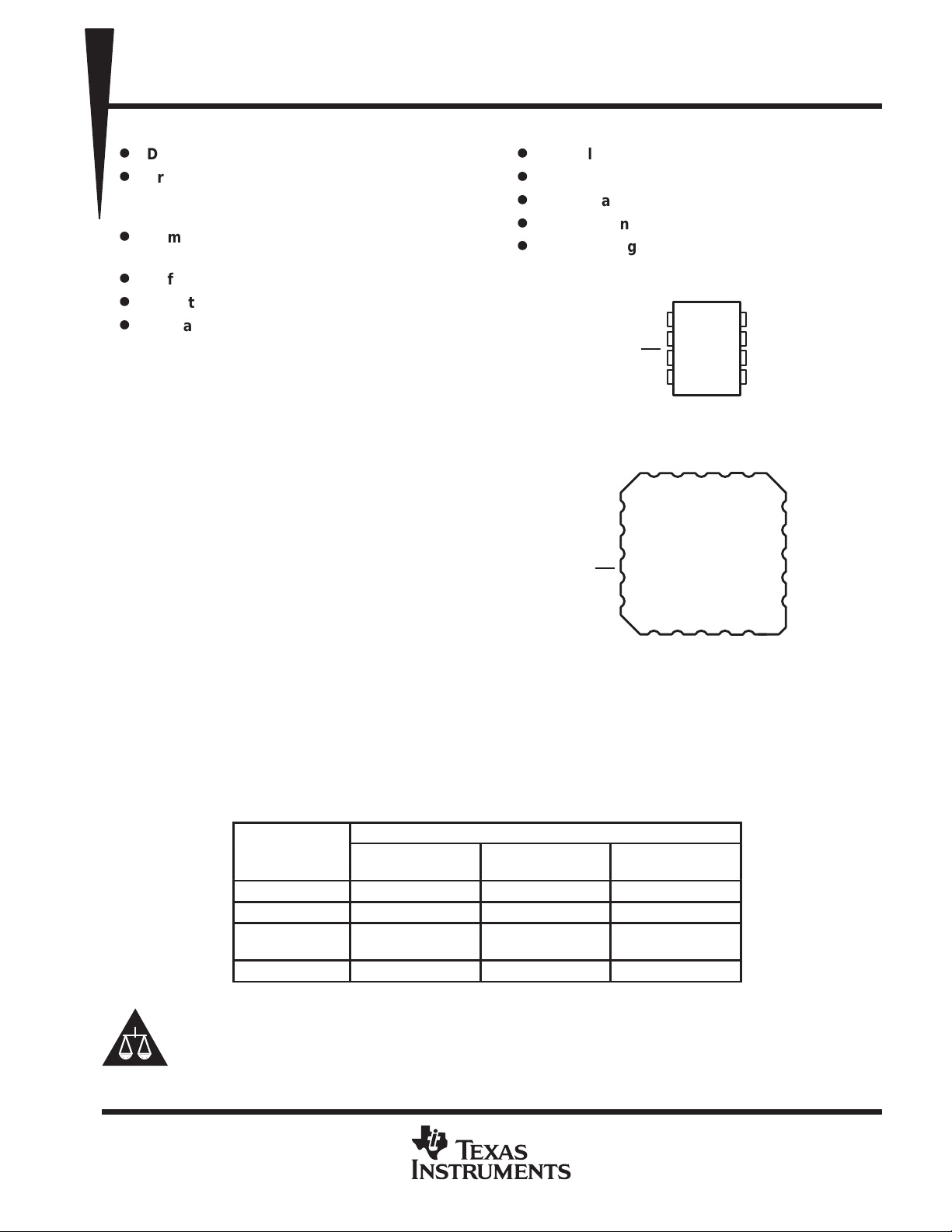
D OR JG PACKAGE
(TOP VIEW)
DIN
NC
SCLK
NC
CS
NC
SCLK
CS
OUTA
4
5
6
7
8
1
2
3
4
FK PACKAGE
(TOP VIEW)
NC
NC
DINNCV
NC
OUTA
8
7
6
5
AGND
DD
1920132
1312119 10
V
DD
OUTB
REF
AGND
NC
18
17
16
15
14
NC
NC
OUTB
NC
REF
NC
Implemented with a CMOS process, the device is designed for single supply operation from 2.7 V to 5.5 V. It
is available in an 8-pin SOIC package in standard commercial and industrial temperature ranges.
The TL V5618AC is characterized for operation from 0°C to 70°C. The TL V5618AI is characterized for operation
from –40°C to 85°C. The TLV5618AQ is characterized for operation from –40°C to 125°C. The TLV5618AM
is characterized for operation from –55°C to 125°C.
AVAILABLE OPTIONS
PACKAGE
T
A
0°C to 70°C TLV5618ACD — —
–40°C to 85°C TLV5618AID — —
–40°C to 125°C
–55°C to 125°C — TLV5618AMJG TLV5618AMFK
Please be aware that an important notice concerning availability, standard warranty, and use in critical applications of
Texas Instruments semiconductor products and disclaimers thereto appears at the end of this data sheet.
SPI and QSPI are trademarks of Motorola, Inc.
Microwire is a trademark of National Semiconductor Corporation.
PRODUCTION DATA information is current as of publication date.
Products conform to specifications per the terms of Texas Instruments
standard warranty. Production processing does not necessarily include
testing of all parameters.
SOIC
(D)
TLV5618AQD
TLV5618AQDR
POST OFFICE BOX 655303 • DALLAS, TEXAS 75265
CERAMIC DIP
(JG)
— —
20 PAD LCCC
(FK)
Copyright 2000, Texas Instruments Incorporated
On products compliant to MIL-PRF-38535, all parameters are tested
unless otherwise noted. On all other products, production
processing does not necessarily include testing of all parameters.
1
TLV5618A
I/O/P
DESCRIPTION
2.7-V TO 5.5-V LOW-POWER DUAL 12-BIT
DIGITAL-TO-ANALOG CONVERTER WITH POWER DOWN
SLAS230D – JULY 1999 – REVISED MARCH 2000
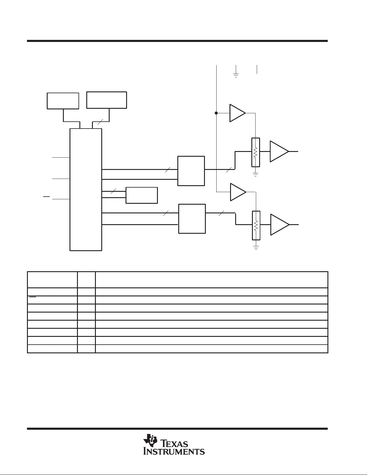
functional block diagram
DIN
SCLK
CS
Power-On
Reset
Speed Control
Serial
Interface
and
Control
Power and
2
12
Buffer
REF AGND V
12 12
12
12-Bit
DAC A
Latch
12-Bit
DAC B
Latch
12
DD
x2
x2
OUTA
OUTB
Terminal Functions
TERMINAL
NAME NO.
AGND 5 P Ground
CS 3 I Chip select. Digital input active low, used to enable/disable inputs.
DIN 1 I Digital serial data input
OUTA 4 O DAC A analog voltage output
OUTB 7 O DAC B analog voltage output
REF 6 I Analog reference voltage input
SCLK 2 I Digital serial clock input
V
DD
8 P Positive power supply
2
POST OFFICE BOX 655303 • DALLAS, TEXAS 75265
PACKAGE
A
A
A
A
Suppl
oltage, V
Operating free-air temperature, T
°C
TLV5618A
2.7-V TO 5.5-V LOW-POWER DUAL 12-BIT
DIGITAL-TO-ANALOG CONVERTER WITH POWER DOWN
SLAS230D – JULY 1999 – REVISED MARCH 2000
absolute maximum ratings over operating free-air temperature range (unless otherwise noted)
Supply voltage (VDD to AGND) 7 V. . . . . . . . . . . . . . . . . . . . . . . . . . . . . . . . . . . . . . . . . . . . . . . . . . . . . . . . . . . . . . .
Reference input voltage range – 0.3 V to VDD + 0.3 V. . . . . . . . . . . . . . . . . . . . . . . . . . . . . . . . . . . . . . . . . . . . . . .
Digital input voltage range – 0.3 V to V
DD
+ 0.3 V. . . . . . . . . . . . . . . . . . . . . . . . . . . . . . . . . . . . . . . . . . . . . . . . . .
Operating free-air temperature range, TA: TLV5618AC 0°C to 70°C. . . . . . . . . . . . . . . . . . . . . . . . . . . . . . . . . . .
TLV5618AI –40°C to 85°C. . . . . . . . . . . . . . . . . . . . . . . . . . . . . . . . . .
TLV5618AQ –40°C to 125°C. . . . . . . . . . . . . . . . . . . . . . . . . . . . . . . .
TLV5618AM –55°C to 125°C. . . . . . . . . . . . . . . . . . . . . . . . . . . . . . . .
Storage temperature range, T
–65°C to 150°C. . . . . . . . . . . . . . . . . . . . . . . . . . . . . . . . . . . . . . . . . . . . . . . . . . .
stg
Lead temperature 1,6 mm (1/16 inch) from case for 10 seconds 260°C. . . . . . . . . . . . . . . . . . . . . . . . . . . . . . .
†
Stresses beyond those listed under “absolute maximum ratings” may cause permanent damage to the device. These are stress ratings only, and
functional operation of the device at these or any other conditions beyond those indicated under “recommended operating conditions” is not
implied. Exposure to absolute-maximum-rated conditions for extended periods may affect device reliability.
DISSIPATION RATING TABLE
T
≤ 25°C DERATING FACTOR T
POWER RATING ABOVE TA = 25°C
D 635 mW 5.08 mW/°C 407 mW 330 mW 127 mW
FK 1375 mW 11.00 mW/°C 880 mW 715 mW 275 mW
JG 1050 mW 8.40 mW/°C 672 mW 546 mW 210 mW
‡
This is the inverse of the traditional junction-to-ambient thermal resistance (RΘJA). Thermal resistances are not production tested and are for
informational purposes only.
‡
= 70°C T
POWER RATING
= 85°C T
POWER RATING
= 125°C
POWER RATING
recommended operating conditions
MIN NOM MAX UNIT
pp
y v
Power on reset, POR 0.55 2 V
High-level digital input voltage, V
Low-level digital input voltage, V
Reference voltage, V
Reference voltage, V
Load resistance, R
Load capacitance, C
Clock frequency, f
p
NOTE 1: Due to the x2 output buffer, a reference input voltage ≥ (VDD–0.4 V)/2 causes clipping of the transfer function.
DD
IH
IL
to REF terminal VDD = 5 V (see Note 1) AGND 2.048 VDD–1.5 V
ref
to REF terminal VDD = 3 V (see Note 1) AGND 1.024 VDD–1.5 V
ref
L
L
CLK
p
A
VDD = 5 V 4.5 5 5.5
VDD = 3 V 2.7 3 3.3
VDD = 2.7 V to 5.5 V 2 V
VDD = 2.7 V to 5.5 V 0.8 V
2 kΩ
100 pF
TLV5618AC 0 70
TLV5618AI –40 85
TLV5618AQ –40 125
TLV5618AM –55 125
V
20 MHz
°
†
POST OFFICE BOX 655303 • DALLAS, TEXAS 75265
3
TLV5618A
I
P
t
All i
AGND
A
DD
y
DD
,
DAC latch = 0x800
Slow
0.8
1
PSRR
Power supply rejection ratio
dB
Reference input bandwidth
REF
V
024 V dc
2.7-V TO 5.5-V LOW-POWER DUAL 12-BIT
DIGITAL-TO-ANALOG CONVERTER WITH POWER DOWN
SLAS230D – JULY 1999 – REVISED MARCH 2000
electrical characteristics over recommended operating conditions (unless otherwise noted)
power supply
PARAMETER TEST CONDITIONS MIN TYP MAX
No load,
ower supply curren
Power down supply current 1 µA
pp
NOTES: 2. Power supply rejection ratio at zero scale is measured by varying VDD and is given by:
PSRR = 20 log [(EZS(VDDmax) – EZS(VDDmin)/VDDmax]
3. Power supply rejection ratio at full scale is measured by varying VDD and is given by:
PSRR = 20 log [(EG(VDDmax) – EG(VDDmin)/VDDmax]
nputs =
Zero scale, See Note 2 –65
Full scale, See Note 3 –65
or V,
=
Fast 1.8 2.3
Slow 0.8 1
static DAC specifications
PARAMETER TEST CONDITIONS MIN TYP MAX UNIT
Resolution 12 bits
INL Integral nonlinearity See Note 4 ±2 ±4 LSB
DNL Differential nonlinearity See Note 5 ±0.5 ±1 LSB
E
ZS
EZS TC Zero-scale-error temperature coefficient See Note 7 3 ppm/°C
E
G
EG T
NOTES: 4. The relative accuracy of integral nonlinearity (INL), sometimes referred to as linearity error , is the maximum deviation of the output
Zero-scale error (offset error at zero scale) See Note 6 ±12 mV
Gain error See Note 8 ±0.6
Gain-error temperature coefficient See Note 9 1 ppm/°C
C
from the line between zero and full scale, excluding the effects of zero-code and full-scale errors.
5. The differential nonlinearity (DNL), sometimes referred to as differential error, is the difference between the measured and ideal
1-LSB amplitude change of any two adjacent codes.
6. Zero-scale error is the deviation from zero voltage output when the digital input code is zero.
7. Zero-scale-error temperature coefficient is given by: EZS TC = [EZS (T
8. Gain error is the deviation from the ideal output (2V
9. Gain temperature coefficient is given by: EG TC = [EG (T
– 1 LSB) with an output load of 10 kΩ.
ref
max) – Eg
(T
max) – EZS
min
)]/2V
(T
× 106/(T
ref
min
)]/2V
max
× 106/(T
ref
– T
min
– T
max
).
output specifications
PARAMETER TEST CONDITIONS MIN TYP MAX UNIT
V
O
Output voltage range RL = 10 kΩ VDD–0.4 V
Output load regulation accuracy VO = 4.096 V, 2.048 V RL = 2 kΩ ±0.29 % FS
min
UNIT
m
% full
scale V
).
reference input
VIInput voltage range 0 V
RIInput resistance 10 MΩ
CIInput capacitance 5 pF
Reference feedthrough REF = 1 Vpp at 1 kHz + 1.024 V dc (see Note 10) –80 dB
NOTE 10: Reference feedthrough is measured at the DAC output with an input code = 0x000.
4
PARAMETER TEST CONDITIONS MIN TYP MAX UNIT
DD–1.5
p
= 0.2
POST OFFICE BOX 655303 • DALLAS, TEXAS 75265
pp
+ 1.
Fast 1.3 MHz
Slow 525 kHz
V
t
Output settling time, full scale
L
,
L
,
s
t
Output settling time, code to code
L
,
L
,
s
SR
Slew rate
L
,
L
,
V/µs
s
,
out
,
dB
TLV5618A
2.7-V TO 5.5-V LOW-POWER DUAL 12-BIT
DIGITAL-TO-ANALOG CONVERTER WITH POWER DOWN
SLAS230D – JULY 1999 – REVISED MARCH 2000
electrical characteristics over recommended operating conditions (unless otherwise noted)
(Continued)
digital inputs
PARAMETER TEST CONDITIONS MIN TYP MAX UNIT
I
High-level digital input current VI = V
IH
I
Low-level digital input current VI = 0 V –1 µA
IL
C
Input capacitance 8 pF
i
DD
analog output dynamic performance
PARAMETER TEST CONDITIONS MIN TYP MAX UNIT
R
s(FS)
s(CC)
SNR Signal-to-noise ratio 76
SINAD Signal-to-noise + distortion
THD Total harmonic distortion
SFDR Spurious free dynamic range 72
NOTES: 11. Settling time is the time for the output signal to remain within ±0.5 LSB of the final measured value for a digital input code change
p
p
Glitch energy
of 0x020 to 0xFDF and 0xFDF to 0x020 respectively. Not tested, assured by design.
12. Settling time is the time for the output signal to remain within ± 0.5 LSB of the final measured value for a digital input code change
of one count. Not tested, assured by design.
13. Slew rate determines the time it takes for a change of the DAC output from 10% to 90% of full-scale voltage.
= 10 kΩ,C
See Note 11
R
= 10 kΩ,C
See Note 12
R
= 10 kΩ,C
See Note 13
DIN = 0 to 1, FCLK = 100 kHz,
CS
= V
DD
f
= 102 kSPS, f
RL = 10 kΩ,CL = 100 pF
= 100 pF,
= 100 pF,
= 100 pF,
= 1 kHz,
Fast 2.5
Slow 12
Fast 1
Slow 2
Fast 3
Slow 0.5
68
–68
1 µA
µ
µ
5 nV–s
POST OFFICE BOX 655303 • DALLAS, TEXAS 75265
5
TLV5618A
t
Setup time, data ready before SCLK falling edge
ns
2.7-V TO 5.5-V LOW-POWER DUAL 12-BIT
DIGITAL-TO-ANALOG CONVERTER WITH POWER DOWN
SLAS230D – JULY 1999 – REVISED MARCH 2000
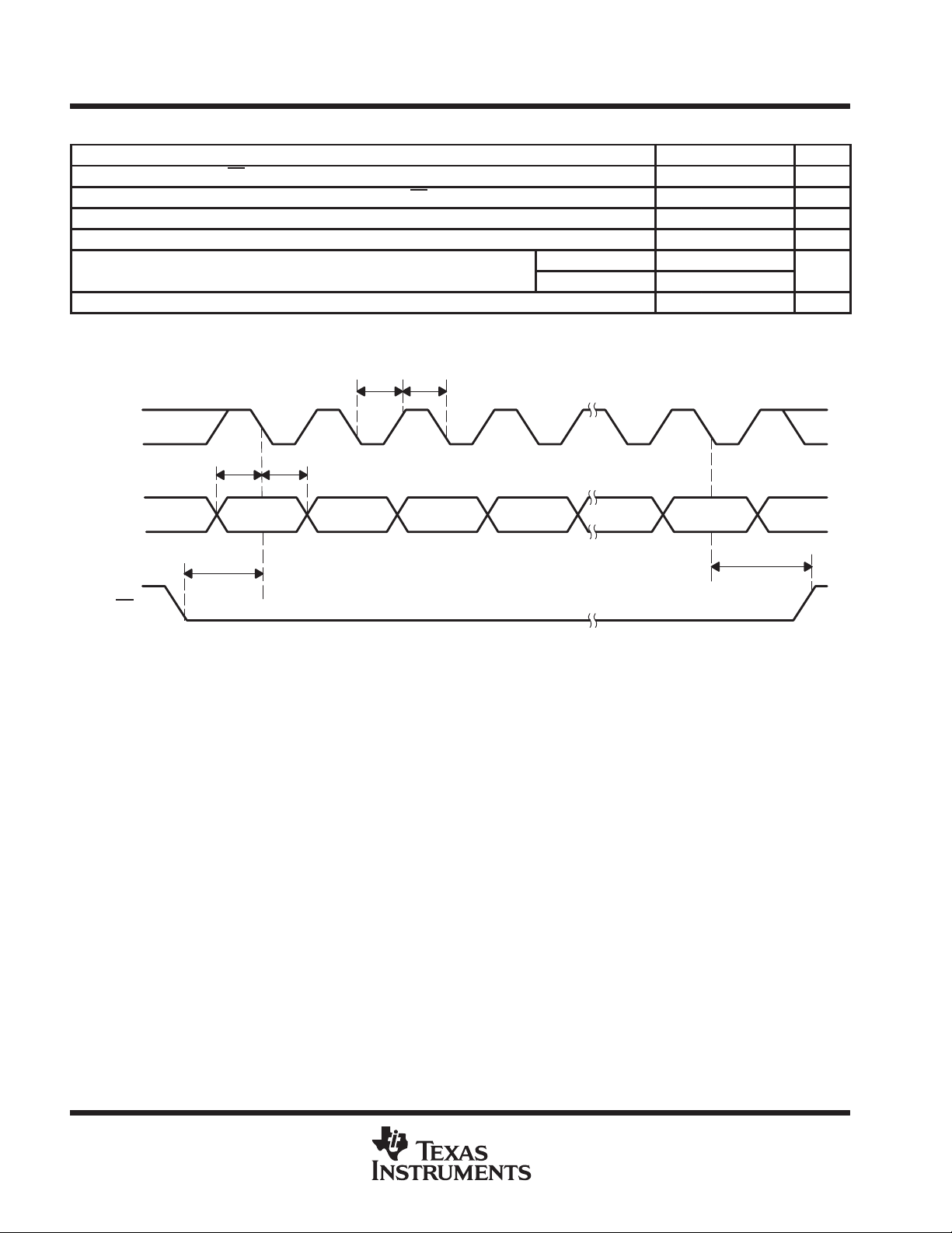
digital input timing requirements
t
su(CS–CK)
t
su(C16-CS)
t
wH
t
wL
su(D)
t
h(D)
timing requirements
Setup time, CS low before first negative SCLK edge 10 ns
Setup time, 16th negative SCLK edge before CS rising edge 10 ns
SCLK pulse width high 25 ns
SCLK pulse width low 25 ns
p
Hold time, data held valid after SCLK falling edge 5 ns
t
t
wL
wH
C and I suffixes 10
Q and M suffixes 8
MIN NOM MAX UNIT
SCLK
DIN
CS
X
t
1
t
su(D)th(D)
su(CS-CK)
2 3 4 5 15 16
D15 D14 D13 D12 D1 D0 XX
t
X
su(C16-CS)
Figure 1. Timing Diagram
6
POST OFFICE BOX 655303 • DALLAS, TEXAS 75265

TLV5618A
2.7-V TO 5.5-V LOW-POWER DUAL 12-BIT
DIGITAL-TO-ANALOG CONVERTER WITH POWER DOWN
SLAS230D – JULY 1999 – REVISED MARCH 2000
TYPICAL CHARACTERISTICS
2.050
2.048
2.046
2.044
2.042
– Output Voltage – V
O
2.040
V
2.038
2.036
0.20
0.18
0.16
0.14
OUTPUT VOLTAGE
vs
LOAD CURRENT
3 V Slow Mode, SOURCE
3 V Fast Mode, SOURCE
0.00 –0.01–0.02–0.05–0.10–0.20–0.51
Load Current - mA
Figure 2
OUTPUT VOLTAGE
vs
LOAD CURRENT
VDD=3 V
V
=1 V
REF
Zero scale
3 V Slow Mode, SINK
VDD=3 V
V
=1 V
REF
Full scale
–1.02–2.05
4.105
4.100
4.095
4.090
4.085
– Output Voltage – V
O
4.080
V
4.075
4.070
0.35
0.30
0.25
OUTPUT VOLTAGE
vs
LOAD CURRENT
5 V Slow Mode, SOURCE
5 V Fast Mode, SOURCE
0.00 –0.02–0.04–0.10–0.20–0.41–1.02
Load Current - mA
Figure 3
OUTPUT VOLTAGE
vs
LOAD CURRENT
VDD=5 V
V
=2 V
REF
Zero scale
5 V Slow Mode, SINK
VDD=5 V
V
=2 V
REF
Full scale
–2.05–4.10
0.12
0.10
0.08
– Output Voltage – V
O
0.06
V
0.04
0.02
0.00
3 V Fast Mode, SINK
0.00 0.01 0.02 0.05 0.10 0.20 0.51
Load Current - mA
Figure 4
0.20
0.15
– Output Voltage – V
O
0.10
V
0.05
1.02 2.05
POST OFFICE BOX 655303 • DALLAS, TEXAS 75265
0.00
0.00 0.02 0.04 0.10 0.20 0.41 1.02
5 V Fast Mode, SINK
2.05 4.09
Load Current - mA
Figure 5
7

TLV5618A
THD
T
t
l
H
i
Di
t
ti
dB
2.7-V TO 5.5-V LOW-POWER DUAL 12-BIT
DIGITAL-TO-ANALOG CONVERTER WITH POWER DOWN
SLAS230D – JULY 1999 – REVISED MARCH 2000
TYPICAL CHARACTERISTICS
SUPPLY CURRENT
vs
FREE-AIR TEMPERATURE
1.8
1.6
1.4
1.2
1.0
0.8
0.6
– Supply Current – mA
DD
I
0.4
0.2
VDD=3 V
V
=1 V
REF
Full scale
Slow Mode
0
–40 –20 0 20 40 60 80 100 120
TA - Free-Air Temperature - C
Fast Mode
Figure 6
TOTAL HARMONIC DISTORTION
vs
FREQUENCY
0
SUPPLY CURRENT
vs
FREE-AIR TEMPERATURE
1.8
1.6
VDD=5 V
1.4
V
=2 V
REF
Full scale
1.2
1.0
0.8
0.6
– Supply Current – mA
DD
I
0.4
0.2
0
–40 –20 0 20 40 60 80 100 120
TA - Free-Air Temperature - C
Fast Mode
Slow Mode
Figure 7
TOTAL HARMONIC DISTORTION
vs
FREQUENCY
0
–10
–20
on or
–30
s
c
–40
–50
armon
a
–60
o
–70
–80
–90
V
= 1 V + 1 V
REF
Output Full Scale
3 V Fast Mode
1 10 100
f - Frequency - kHz
Sinewave,
P/P
5 V Fast Mode
Figure 8
V
= 1 V + 1 V
–10
–20
–30
–40
–50
–60
–70
THD - Total Harmonic Distortion - dB
–80
–90
REF
Output Full Scale
3 V Slow Mode
1 10 100
Sinewave,
P/P
5 V Slow Mode
f - Frequency - kHz
Figure 9
8
POST OFFICE BOX 655303 • DALLAS, TEXAS 75265

TLV5618A
2.7-V TO 5.5-V LOW-POWER DUAL 12-BIT
DIGITAL-TO-ANALOG CONVERTER WITH POWER DOWN
SLAS230D – JULY 1999 – REVISED MARCH 2000
TYPICAL CHARACTERISTICS
INTEGRAL NONLINEARITY ERROR
vs
DIGITAL CODE
4.0
3.5
3.0
2.5
2.0
1.5
1.0
0.5
0.0
–0.5
–1.0
–1.5
–2.0
–2.5
–3.0
–3.5
–4
0 512 1024 1536 2048 2560 3072 3584 4096
INL - Integral Nonlinearity Error - LSB
Digital Code
Figure 10
1.00
0.75
0.50
0.25
0.00
–0.25
–0.50
–0.75
–1
DNL – Differential Nonlinearity – LSB
0 4096
DIFFERENTIAL NONLINEARITY ERROR
vs
DIGITAL CODE
20481024 3072
Digital Code
Figure 11
POST OFFICE BOX 655303 • DALLAS, TEXAS 75265
9

TLV5618A
2.7-V TO 5.5-V LOW-POWER DUAL 12-BIT
DIGITAL-TO-ANALOG CONVERTER WITH POWER DOWN
SLAS230D – JULY 1999 – REVISED MARCH 2000
APPLICATION INFORMATION
general function
The TL V5618A is a dual 12-bit, single-supply DAC, based on a resistor-string architecture. It consists of a serial
interface, a speed and power down control logic, a resistor string, and a rail-to-rail output buffer.
The output voltage (full scale determined by the reference) is given by:
2REF
CODE
0x1000
[V]
Where REF is the reference voltage and CODE is the digital input value in the range 0x000 to 0xFFF . A power-on
reset initially puts the internal latches to a defined state (all bits zero).
serial interface
A falling edge of CS starts shifting the data bit-per-bit (starting with the MSB) to the internal register on the falling
edges of SCLK. After 16 bits have been transferred or CS
rises, the content of the shift register is moved to the
target latches (DAC A, DAC B, BUFFER, CONTROL), depending on the control bits within the data word.
Figure 12 shows examples of how to connect the TLV5618A to TMS320, SPI, and Microwire.
TMS320
DSP
CLKX
FSX
DX
TLV5618A
CS
DIN
SCLK
SPI
I/O
MOSI
SCK
TLV5618A
CS
DIN
SCLK
Microwire
I/O
SO
SK
CS
DIN
SCLK
Figure 12. Three-Wire Interface
Notes on SPI and Microwire: Before the controller starts the data transfer, the software has to generate a
falling edge on the pin connected to CS
. If the word width is 8 bits (SPI and Microwire) two write operations
must be performed to program the TL V5618A. After the write operation(s), the holding registers or the control
register are updated automatically on the 16th positive clock edge.
serial clock frequency and update rate
TLV5618A
The maximum serial clock frequency is given by:
f
sclkmax
+
t
whmin
1
)
t
wlmin
+
20 MHz
The maximum update rate is:
whmin
1
)
t
wlmin
+
Ǔ
1.25 MHz
f
updatemax
+
16ǒt
Note that the maximum update rate is just a theoretical value for the serial interface, as the settling time of the
TLV5618A should also be considered.
10
POST OFFICE BOX 655303 • DALLAS, TEXAS 75265

TLV5618A
2.7-V TO 5.5-V LOW-POWER DUAL 12-BIT
DIGITAL-TO-ANALOG CONVERTER WITH POWER DOWN
SLAS230D – JULY 1999 – REVISED MARCH 2000
APPLICATION INFORMATION
data format
The 16-bit data word for the TLV5618A consists of two parts:
D
Program bits (D15..D12)
D
New data (D11..D0)
D15 D14 D13 D12 D11 D10 D9 D8 D7 D6 D5 D4 D3 D2 D1 D0
R1 SPD PWR R0 MSB 12 Data bits LSB
SPD: Speed control bit 1 → fast mode 0 →slow mode
PWR: Power control bit 1 → power down 0 → normal operation
On power up, SPD and PWD are reset to 0 (slow mode and normal operation)
The following table lists all possible combination of register-select bits:
register-select bits
R1 R0 REGISTER
0 0 Write data to DAC B and BUFFER
0 1 Write data to BUFFER
1 0 Write data to DAC A and update DAC B with BUFFER content
1 1 Reserved
The meaning of the 12 data bits depends on the register. If one of the DAC registers or the BUFFER is selected,
then the 12 data bits determine the new DAC value:
examples of operation
D
Set DAC A output, select fast mode:
Write new DAC A value and update DAC A output:
D15 D14 D13 D12 D11 D10 D9 D8 D7 D6 D5 D4 D3 D2 D1 D0
1 1 0 0 New DAC A output value
The DAC A output is updated on the rising clock edge after D0 is sampled.
D
Set DAC B output, select fast mode:
Write new DAC B value to BUFFER and update DAC B output:
D15 D14 D13 D12 D11 D10 D9 D8 D7 D6 D5 D4 D3 D2 D1 D0
0 1 0 0 New BUFFER content and DAC B output value
The DAC A output is updated on the rising clock edge after D0 is sampled.
D
Set DAC A value, set DAC B value, update both simultaneously, select slow mode:
1. Write data for DAC B to BUFFER:
D15 D14 D13 D12 D11 D10 D9 D8 D7 D6 D5 D4 D3 D2 D1 D0
0 0 0 1 New DAC B value
2. Write new DAC A value and update DAC A and B simultaneously:
D15 D14 D13 D12 D11 D10 D9 D8 D7 D6 D5 D4 D3 D2 D1 D0
1 0 0 0 New DAC A value
POST OFFICE BOX 655303 • DALLAS, TEXAS 75265
11

TLV5618A
2.7-V TO 5.5-V LOW-POWER DUAL 12-BIT
DIGITAL-TO-ANALOG CONVERTER WITH POWER DOWN
SLAS230D – JULY 1999 – REVISED MARCH 2000
APPLICATION INFORMATION
examples of operation (continued)
Both outputs are updated on the rising clock edge after D0 from the DAC A data word is sampled.
D
Set power-down mode:
D15 D14 D13 D12 D11 D10 D9 D8 D7 D6 D5 D4 D3 D2 D1 D0
X X 1 X X X X X X X X X X X X X
X = Don’t care
linearity, offset, and gain error using single ended supplies
When an amplifier is operated from a single supply , the voltage offset can still be either positive or negative. With
a positive offset, the output voltage changes on the first code change. With a negative offset, the output voltage
may not change with the first code, depending on the magnitude of the offset voltage.
The output amplifier attempts to drive the output to a negative voltage. However, because the most negative
supply rail is ground, the output cannot drive below ground and clamps the output at 0 V.
The output voltage then remains at zero until the input code value produces a sufficient positive output voltage
to overcome the negative offset voltage, resulting in the transfer function shown in Figure 13.
Output
Voltage
0 V
Negative
Offset
DAC Code
Figure 13. Effect of Negative Offset (Single Supply)
This offset error , not the linearity error, produces this breakpoint. The transfer function would have followed the
dotted line if the output buffer could drive below the ground rail.
For a DAC, linearity is measured between zero-input code (all inputs 0) and full-scale code (all inputs 1) after
offset and full scale are adjusted out or accounted for in some way . However , single supply operation does not
allow for adjustment when the offset is negative due to the breakpoint in the transfer function. So the linearity
is measured between full-scale code and the lowest code that produces a positive output voltage.
definitions of specifications and terminology
integral nonlinearity (INL)
The relative accuracy or integral nonlinearity (INL), sometimes referred to as linearity error, is the maximum
deviation of the output from the line between zero and full scale excluding the effects of zero code and full-scale
errors.
differential nonlinearity (DNL)
The differential nonlinearity (DNL), sometimes referred to as differential error, is the difference between the
measured and ideal 1 LSB amplitude change of any two adjacent codes. Monotonic means the output voltage
changes in the same direction (or remains constant) as a change in the digital input code.
12
POST OFFICE BOX 655303 • DALLAS, TEXAS 75265

2.7-V TO 5.5-V LOW-POWER DUAL 12-BIT
DIGITAL-TO-ANALOG CONVERTER WITH POWER DOWN
SLAS230D – JULY 1999 – REVISED MARCH 2000
definitions of specifications and terminology (continued)
zero-scale error (EZS)
Zero-scale error is defined as the deviation of the output from 0 V at a digital input value of 0.
gain error (EG)
Gain error is the error in slope of the DAC transfer function.
total harmonic distortion (THD)
THD is the ratio of the rms value of the first six harmonic components to the value of the fundamental signal.
The value for THD is expressed in decibels.
signal-to-noise ratio + distortion (S/N+D)
S/N+D is the ratio of the rms value of the output signal to the rms sum of all other spectral components below
the Nyquist frequency, including harmonics but excluding dc. The value for S/N+D is expressed in decibels.
spurious free dynamic range (SFDR)
Spurious free dynamic range is the difference between the rms value of the output signal and the rms value of
the largest spurious signal within a specified bandwidth. The value for SFDR is expressed in decibels.
TLV5618A
POST OFFICE BOX 655303 • DALLAS, TEXAS 75265
13

TLV5618A
2.7-V TO 5.5-V LOW-POWER DUAL 12-BIT
DIGITAL-TO-ANALOG CONVERTER WITH POWER DOWN
SLAS230D – JULY 1999 – REVISED MARCH 2000
MECHANICAL DATA
D (R-PDSO-G**) PLASTIC SMALL-OUTLINE PACKAGE
14 PIN SHOWN
0.050 (1,27)
14
1
0.069 (1,75) MAX
0.020 (0,51)
0.014 (0,35)
8
7
A
0.010 (0,25)
0.004 (0,10)
DIM
0.157 (4,00)
0.150 (3,81)
PINS **
0.010 (0,25)
0.244 (6,20)
0.228 (5,80)
8
M
Seating Plane
0.004 (0,10)
14
0.008 (0,20) NOM
0°–8°
16
Gage Plane
0.010 (0,25)
0.044 (1,12)
0.016 (0,40)
A MAX
A MIN
NOTES: A. All linear dimensions are in inches (millimeters).
14
B. This drawing is subject to change without notice.
C. Body dimensions do not include mold flash or protrusion, not to exceed 0.006 (0,15).
D. Falls within JEDEC MS-012
POST OFFICE BOX 655303 • DALLAS, TEXAS 75265
0.197
(5,00)
0.189
(4,80)
0.344
(8,75)
0.337
(8,55)
0.394
(10,00)
0.386
(9,80)
4040047/D 10/96

TLV5618A
2.7-V TO 5.5-V LOW-POWER DUAL 12-BIT
DIGITAL-TO-ANALOG CONVERTER WITH POWER DOWN
SLAS230D – JULY 1999 – REVISED MARCH 2000
MECHANICAL DATA
FK (S-CQCC-N**) LEADLESS CERAMIC CHIP CARRIER
28 TERMINALS SHOWN
A SQ
B SQ
19
20
21
22
23
24
25
12826 27
12
1314151618 17
0.020 (0,51)
0.010 (0,25)
MIN
0.342
(8,69)
0.442
0.640
0.740
0.938
1.141
A
0.358
(9,09)
0.458
(11,63)
0.660
(16,76)
0.761
(19,32)(18,78)
0.962
(24,43)
1.165
(29,59)
NO. OF
TERMINALS
**
11
10
9
8
7
6
5
432
20
28
44
52
68
84
0.020 (0,51)
0.010 (0,25)
(11,23)
(16,26)
(23,83)
(28,99)
MINMAX
0.307
(7,80)
0.406
(10,31)
0.495
(12,58)
0.495
(12,58)
0.850
(21,6)
1.047
(26,6)
0.080 (2,03)
0.064 (1,63)
B
MAX
0.358
(9,09)
0.458
(11,63)
0.560
(14,22)
0.560
(14,22)
0.858
(21,8)
1.063
(27,0)
0.055 (1,40)
0.045 (1,14)
0.028 (0,71)
0.022 (0,54)
0.050 (1,27)
NOTES: A. All linear dimensions are in inches (millimeters).
B. This drawing is subject to change without notice.
C. This package can be hermetically sealed with a metal lid.
D. The terminals are gold-plated.
E. Falls within JEDEC MS-004
POST OFFICE BOX 655303 • DALLAS, TEXAS 75265
0.045 (1,14)
0.035 (0,89)
0.045 (1,14)
0.035 (0,89)
4040140/C 11/95
15

MECHANICAL DATA
MCER001A – JANUARY 1995 – REVISED JANUARY 1997
MECHANICAL DATA
JG (R-GDIP-T8) CERAMIC DUAL-IN-LINE
0.400 (10,16)
0.355 (9,00)
0.063 (1,60)
0.015 (0,38)
0.100 (2,54)
8
1
5
4
0.065 (1,65)
0.045 (1,14)
0.020 (0,51) MIN
0.023 (0,58)
0.015 (0,38)
0.280 (7,11)
0.245 (6,22)
0.310 (7,87)
0.290 (7,37)
0.200 (5,08) MAX
Seating Plane
0.130 (3,30) MIN
0°–15°
0.014 (0,36)
0.008 (0,20)
NOTES: A. All linear dimensions are in inches (millimeters).
16
B. This drawing is subject to change without notice.
C. This package can be hermetically sealed with a ceramic lid using glass frit.
D. Index point is provided on cap for terminal identification.
E. Falls within MIL STD 1835 GDIP1-T8
POST OFFICE BOX 655303 • DALLAS, TEXAS 75265
4040107/C 08/96

MCER001A – JANUARY 1995 – REVISED JANUARY 1997
MECHANICAL DATA
MECHANICAL DATA
P (R-PDIP-T8) PLASTIC DUAL-IN-LINE PACKAGE
0.400 (10,60)
0.355 (9,02)
58
0.260 (6,60)
0.240 (6,10)
41
0.070 (1,78) MAX
0.020 (0,51) MIN
0.200 (5,08) MAX
0.125 (3,18) MIN
0.100 (2,54)
0.021 (0,53)
0.015 (0,38)
NOTES: A. All linear dimensions are in inches (millimeters).
B. This drawing is subject to change without notice.
C. Falls within JEDEC MS-001
0.010 (0,25)
M
0.310 (7,87)
0.290 (7,37)
Seating Plane
0°–15°
0.010 (0,25) NOM
4040082/B 03/95
POST OFFICE BOX 655303 • DALLAS, TEXAS 75265
17

IMPORTANT NOTICE
T exas Instruments and its subsidiaries (TI) reserve the right to make changes to their products or to discontinue
any product or service without notice, and advise customers to obtain the latest version of relevant information
to verify, before placing orders, that information being relied on is current and complete. All products are sold
subject to the terms and conditions of sale supplied at the time of order acknowledgement, including those
pertaining to warranty, patent infringement, and limitation of liability.
TI warrants performance of its semiconductor products to the specifications applicable at the time of sale in
accordance with TI’s standard warranty. Testing and other quality control techniques are utilized to the extent
TI deems necessary to support this warranty . Specific testing of all parameters of each device is not necessarily
performed, except those mandated by government requirements.
CERTAIN APPLICA TIONS USING SEMICONDUCT OR PRODUCTS MAY INVOLVE POTENTIAL RISKS OF
DEATH, PERSONAL INJURY, OR SEVERE PROPERTY OR ENVIRONMENTAL DAMAGE (“CRITICAL
APPLICATIONS”). TI SEMICONDUCTOR PRODUCTS ARE NOT DESIGNED, AUTHORIZED, OR
WARRANTED TO BE SUITABLE FOR USE IN LIFE-SUPPORT DEVICES OR SYSTEMS OR OTHER
CRITICAL APPLICA TIONS. INCLUSION OF TI PRODUCTS IN SUCH APPLICATIONS IS UNDERST OOD TO
BE FULLY AT THE CUSTOMER’S RISK.
In order to minimize risks associated with the customer’s applications, adequate design and operating
safeguards must be provided by the customer to minimize inherent or procedural hazards.
TI assumes no liability for applications assistance or customer product design. TI does not warrant or represent
that any license, either express or implied, is granted under any patent right, copyright, mask work right, or other
intellectual property right of TI covering or relating to any combination, machine, or process in which such
semiconductor products or services might be or are used. TI’s publication of information regarding any third
party’s products or services does not constitute TI’s approval, warranty or endorsement thereof.
Copyright 2000, Texas Instruments Incorporated
 Loading...