

Datasheet TLV5606IDR, TLV5606IDGKR, TLV5606IDGK, TLV5606ID, TLV5606CDGKR Datasheet (Texas Instruments)
...
features
D
10-Bit Voltage Output DAC
D
Programmable Settling Time vs Power
Consumption
3 µs in Fast Mode
9 µs in Slow Mode
D
Ultra Low Power Consumption:
900 µW Typ in Slow Mode at 3 V
2.1 mW Typ in Fast Mode at 3 V
D
Differential Nonlinearity . . . <0.2 LSB Typ
D
Compatible With TMS320 and SPI Serial
Ports
D
Power-Down Mode (10 nA)
description
The TL V5606 is a 10-bit voltage output digital-toanalog converter (DAC) with a flexible 4-wire
serial interface. The 4-wire serial interface allows
glueless interface to TMS320, SPI, QSPI, and
Microwire serial ports. The TLV5606 is programmed with a 16-bit serial string containing 4
control and 10 data bits. Developed for a wide
range of supply voltages, the TLV5606 can
operate from 2.7 V to 5.5 V.
TLV5606
2.7 V TO 5.5 V LOW POWER 10-BIT DIGITAL-TO-ANALOG
CONVERTERS WITH POWER DOWN
SLAS259 – DECEMBER 1999
D
Buffered High-Impedance Reference Input
D
Voltage Output Range ... 2 Times the
Reference Input Voltage
D
Monotonic Over Temperature
D
Available in MSOP Package
applications
D
Digital Servo Control Loops
D
Digital Offset and Gain Adjustment
D
Industrial Process Control
D
Machine and Motion Control Devices
D
Mass Storage Devices
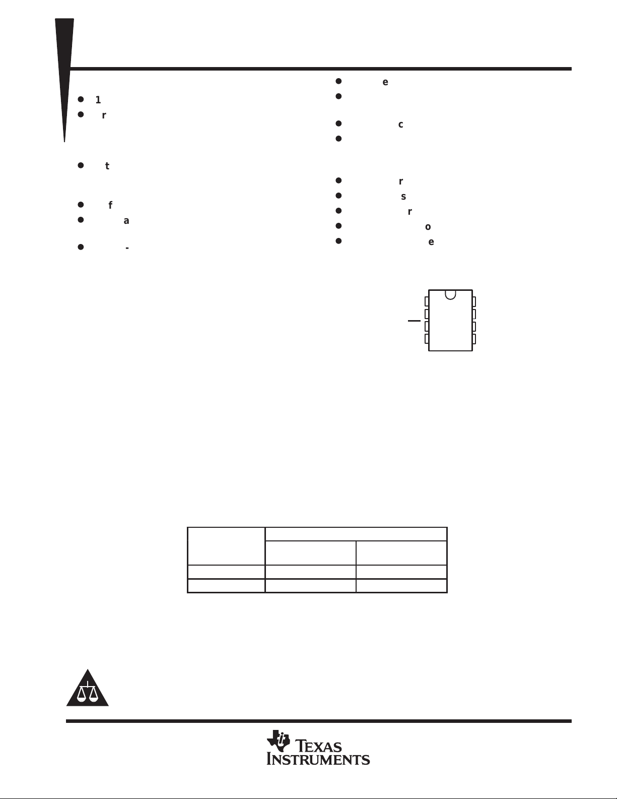
D OR DGK PACKAGE
(TOP VIEW)
DIN
SCLK
CS
FS
1
2
3
4
8
7
6
5
V
DD
OUT
REFIN
AGND
The resistor string output voltage is buffered by a x2 gain rail-to-rail output buffer . The buffer features a Class AB
output stage to improve stability and reduce settling time. The settling time of the DAC is programmable to allow
the designer to optimize speed versus power dissipation. The settling time is chosen by the control bits within
the 16-bit serial input string. A high-impedance buffer is integrated on the REFIN terminal to reduce the need
for a low source impedance drive to the terminal.
Implemented with a CMOS process, the TL V5606 is designed for single supply operation from 2.7 V to 5.5 V.
The device is available in an 8-terminal SOIC package. The TL V5606C is characterized for operation from 0°C
to 70°C. The TLV5606I is characterized for operation from –40°C to 85°C.
AVAILABLE OPTIONS
PACKAGE
T
A
0°C to 70°C TLV5606CD TLV5606CDGK
–40°C to 85°C TLV5606ID TLV5606IDGK
†
Available in tape and reel as the TL V5606CDR, TL V5606IDR,
TLV5606CDGKR, and the TLV5606IDGKR
Please be aware that an important notice concerning availability, standard warranty, and use in critical applications of
Texas Instruments semiconductor products and disclaimers thereto appears at the end of this data sheet.
SMALL OUTLINE
(D)
†
MSOP
(DGK)
†
PRODUCTION DATA information is current as of publication date.
Products conform to specifications per the terms of Texas Instruments
standard warranty. Production processing does not necessarily include
testing of all parameters.
POST OFFICE BOX 655303 • DALLAS, TEXAS 75265
Copyright 1999, Texas Instruments Incorporated
1
TLV5606
I/O
DESCRIPTION
2.7 V TO 5.5 V LOW POWER 10-BIT DIGITAL-TO-ANALOG
CONVERTERS WITH POWER DOWN
SLAS259 – DECEMBER 1999
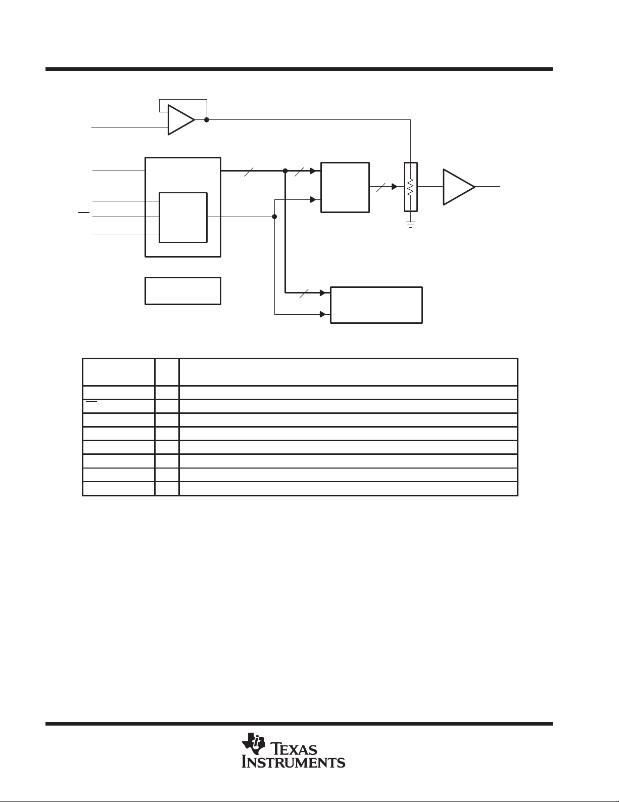
functional block diagram
_
REFIN
6
+
DIN
SCLK
CS
FS
1
2
3
4
Serial Input
Register
16 Cycle
Timer
Power-On
Reset
12
Update
10
10-Bit
Data
Latch
2
Speed/Power-Down
10
Logic
x2
Terminal Functions
TERMINAL
NAME NO.
AGND 5 Analog ground
CS 3 I Chip select. Digital input used to enable and disable inputs, active low.
DIN 1 I Serial digital data input
FS 4 I Frame sync. Digital input used for 4-wire serial interfaces such as the TMS320 DSP interface.
OUT 7 O DAC analog output
REFIN 6 I Reference analog input voltage
SCLK 2 I Serial digital clock input
V
DD
8 Positive power supply
7
OUT
2
POST OFFICE BOX 655303 • DALLAS, TEXAS 75265
Suppl
oltage, V
Operating free-air temperature, T
IDDPower supply current
PSRR
Power supply rejection ratio
dB
TLV5606
2.7 V TO 5.5 V LOW POWER 10-BIT DIGITAL-TO-ANALOG
CONVERTERS WITH POWER DOWN
SLAS259 – DECEMBER 1999
absolute maximum ratings over operating free-air temperature range (unless otherwise noted)
Supply voltage (VDD to AGND) 7 V. . . . . . . . . . . . . . . . . . . . . . . . . . . . . . . . . . . . . . . . . . . . . . . . . . . . . . . . . . . . . . .
Reference input voltage range – 0.3 V to VDD + 0.3 V. . . . . . . . . . . . . . . . . . . . . . . . . . . . . . . . . . . . . . . . . . . . . . .
Digital input voltage range – 0.3 V to V
DD
+ 0.3 V. . . . . . . . . . . . . . . . . . . . . . . . . . . . . . . . . . . . . . . . . . . . . . . . . .
Operating free-air temperature range, TA: TLV5606C 0°C to 70°C. . . . . . . . . . . . . . . . . . . . . . . . . . . . . . . . . . . .
TLV5606I –40°C to 85°C. . . . . . . . . . . . . . . . . . . . . . . . . . . . . . . . . . .
Storage temperature range, T
–65°C to 150°C. . . . . . . . . . . . . . . . . . . . . . . . . . . . . . . . . . . . . . . . . . . . . . . . . . .
stg
Lead temperature 1,6 mm (1/16 inch) from case for 10 seconds 260°C. . . . . . . . . . . . . . . . . . . . . . . . . . . . . . .
†
Stresses beyond those listed under “absolute maximum ratings” may cause permanent damage to the device. These are stress ratings only, and
functional operation of the device at these or any other conditions beyond those indicated under “recommended operating conditions” is not
implied. Exposure to absolute-maximum-rated conditions for extended periods may affect device reliability.
recommended operating conditions
MIN NOM MAX UNIT
pp
y v
High-level digital input voltage, V
Low-level digital input voltage, V
Reference voltage, V
Reference voltage, V
Load resistance, R
Load capacitance, C
Clock frequency, f
p
NOTE 1: Due to the x2 output buffer, a reference input voltage ≥ V
DD
IH
IL
to REFIN terminal VDD = 5 V (see Note 1) AGND 2.048 VDD–1.5 V
ref
to REFIN terminal VDD = 3 V (see Note 1) AGND 1.024 VDD–1.5 V
ref
L
L
CLK
p
A
VDD = 5 V 4.5 5 5.5 V
VDD = 3 V 2.7 3 3.3 V
VDD = 2.7 V to 5.5 V 2 V
VDD = 2.7 V to 5.5 V 0.8 V
2 10 kΩ
100 pF
20 MHz
TLV5606C 0 70 °C
TLV5606I –40 85 °C
causes clipping of the transfer function.
DD/2
†
electrical characteristics over recommended operating free-air temperature range (unless
otherwise noted)
power supply
PARAMETER TEST CONDITIONS MIN TYP MAX
VDD = 5 V, VREF = 2.048 V,
No load,
All inputs = AGND or VDD,
pp
Power down supply current (see Figure 12) 10 nA
pp
Power on threshold voltage, POR 2 V
NOTES: 2. Power supply rejection ratio at zero scale is measured by varying VDD and is given by:
PSRR = 20 log [(EZS(VDDmax) – EZS(VDDmin))/VDDmax]
3. Power supply rejection ratio at full scale is measured by varying VDD and is given by:
PSRR = 20 log [(EG(VDDmax) – EG(VDDmin))/VDDmax]
Zero scale See Note 2 –80
Full scale See Note 3 –80
DAC latch = 0x800
VDD = 3 V, VREF = 1.024 V
No load,
All inputs = AGND or VDD,
DAC latch = 0x800
Fast 0.9 1.35 mA
Slow 0.4 0.6 mA
Fast 0.7 1.1 mA
Slow 0.3 0.45 mA
UNIT
POST OFFICE BOX 655303 • DALLAS, TEXAS 75265
3
TLV5606
Reference input bandwidth
REFIN
V
1.024 V dc
2.7 V TO 5.5 V LOW POWER 10-BIT DIGITAL-TO-ANALOG
CONVERTERS WITH POWER DOWN
SLAS259 – DECEMBER 1999
electrical characteristics over recommended operating free-air temperature range (unless
otherwise noted) (continued)
static DAC specifications RL = 10 kΩ, CL = 100 pF
PARAMETER TEST CONDITIONS MIN TYP MAX UNIT
Resolution 10 10 bits
INL Integral nonlinearity See Note 4 ± 0.5 ±1.5 LSB
DNL Differential nonlinearity See Note 5 ± 0.2 ± 1 LSB
E
Zero-scale error (offset error at zero scale) See Note 6 ±10 mV
ZS
Zero-scale-error temperature coefficient See Note 7 10 ppm/°C
% of
E
Gain error See Note 8 ±0.6
G
Gain-error temperature coefficient See Note 9 10 ppm/°C
NOTES: 4. The relative accuracy or integral nonlinearity (INL) sometimes referred to as linearity error , is the maximum deviation of the output
from the line between zero and full scale excluding the effects of zero code and full-scale errors.
5. The differential nonlinearity (DNL) sometimes referred to as differential error, is the difference between the measured and ideal 1
LSB amplitude change of any two adjacent codes. Monotonic means the output voltage changes in the same direction (or remains
constant) as a change in the digital input code.
6. Zero-scale error is the deviation from zero voltage output when the digital input code is zero.
7. Zero-scale-error temperature coefficient is given by: EZSTC = [EZS(T
8. Gain error is the deviation from the ideal output (2V
9. Gain temperature coefficient is given by: EGTC = [EG(T
– 1 LSB) with an output load of 10 kΩ excluding the effects of the zero-error .
ref
max
) – EG (T
max
min
) – EZS(T
)]/V
× 106/(T
ref
min
)]/V
max
× 106/(T
ref
– T
min
– T
max
min
).
output specifications
PARAMETER TEST CONDITIONS MIN TYP MAX UNIT
V
Voltage output range RL = 10 kΩ 0 AVDD–0.1 V
O
Output load regulation accuracy RL = 2 kΩ, vs 10 kΩ 0.1 ±0.25
FS
voltage
).
% of FS
voltage
reference input (REF)
PARAMETER TEST CONDITIONS MIN TYP MAX UNIT
V
Input voltage range 0 VDD–1.5 V
I
R
Input resistance 10 MΩ
I
C
Input capacitance 5 pF
I
p
Reference feed through REFIN = 1 Vpp at 1 kHz + 1.024 V dc (see Note 10) –75 dB
NOTE 10: Reference feedthrough is measured at the DAC output with an input code = 0x000.
= 0.2
pp
+
Slow 525 kHz
Fast 1.3 MHz
digital inputs
PARAMETER TEST CONDITIONS MIN TYP MAX UNIT
I
High-level digital input current VI = V
IH
I
Low-level digital input current VI = 0 V ±1 µA
IL
C
Input capacitance 3 pF
I
DD
±1 µA
4
POST OFFICE BOX 655303 • DALLAS, TEXAS 75265
t
Output settling time, full scale
L
,
s
t
Output settling time, code to code
L
,
SR
Slew rate
L
,
L
,
V/µs
R
10 kΩ,C
100 pF
0
BW = 20 kHz
TLV5606
2.7 V TO 5.5 V LOW POWER 10-BIT DIGITAL-TO-ANALOG
CONVERTERS WITH POWER DOWN
SLAS259 – DECEMBER 1999
operating characteristics over recommended operating free-air temperature range (unless
otherwise noted)
analog output dynamic performance
PARAMETER TEST CONDITIONS MIN TYP MAX UNIT
kHz
CL = 100 pF,
CL = 100 pF,
= 100 pF,
=
p
L
R
s(FS)
s(CC)
S/N Signal to noise 62 dB
S/(N+D) Signal to noise + distortion
THD Total harmonic distortion
NOTES: 11. Settling time is the time for the output signal to remain within ±0.5 LSB of the final measured value for a digital input code change
p
p
Glitch energy Code transition from 0x7FF to 0x800 10 nV–s
Spurious free dynamic range
of 0x080 to 0x3FF or 0x3FF to 0x080. Not tested, ensured by design.
12. Settling time is the time for the output signal to remain within ± 0.5 LSB of the final measured value for a digital input code change
of one count. Code change from 0x1FF to 0x200. Not tested, ensured by design.
13. Slew rate determines the time it takes for a change of the DAC output from 10% to 90% full-scale voltage.
= 10 kΩ,
See Note 11
R
= 10 kΩ,
See Note 12
R
= 10 kΩ, C
See Note 13
fs = 400 KSPS fout = 1.1 kHz,
=
L
BW = 2
Fast 3 5.5
Slow 9 20
Fast 1 µs
Slow 2 µs
Fast 3.6
Slow 0.9
,
–61 dB
µ
60 dB
68 dB
digital input timing requirements
t
su(CS–FS)
t
su(FS–CK)
t
su(C16–FS)
t
su(C16–CS)
t
wH
t
wL
t
su(D)
t
h(D)
t
wH(FS)
Setup time, CS low before FS↓ 10 ns
Setup time, FS low before first negative SCLK edge 8 ns
Setup time, sixteenth negative edge after FS low on which bit D0 is sampled before rising
edge of FS
Setup time, sixteenth positive SCLK edge (first positive after D0 is sampled) before CS rising
edge. If FS is used instead of the sixteenth positive edge to update the DAC, then the setup
time is between the FS rising edge and CS
Pulse duration, SCLK high 25 ns
Pulse duration, SCLK low 25 ns
Setup time, data ready before SCLK falling edge 8 ns
Hold time, data held valid after SCLK falling edge 5 ns
Pulse duration, FS high 20 ns
MIN NOM MAX UNIT
10 ns
10 ns
rising edge.
POST OFFICE BOX 655303 • DALLAS, TEXAS 75265
5
TLV5606
2.7 V TO 5.5 V LOW POWER 10-BIT DIGITAL-TO-ANALOG
CONVERTERS WITH POWER DOWN
SLAS259 – DECEMBER 1999
PARAMETER MEASUREMENT INFORMATION
SCLK
DIN
CS
FS
t
su(D)
t
wL
123451516
t
h(D)
D15 D14 D13 D12 D1 D0
t
su(FS-CK)
t
su(CS-FS)
t
wH(FS)
t
wH
t
t
su(C16-FS)
su(C16-CS)
Figure 1. Timing Diagram
6
POST OFFICE BOX 655303 • DALLAS, TEXAS 75265
TLV5606
2.7 V TO 5.5 V LOW POWER 10-BIT DIGITAL-TO-ANALOG
CONVERTERS WITH POWER DOWN
SLAS259 – DECEMBER 1999
TYPICAL CHARACTERISTICS
2.004
2.002
2
1.998
1.996
– Output Voltage – V
1.994
O
V
1.992
1.990
0.2
0.18
0.16
0.14
0.12
0.1
0.08
– Output Voltage – V
0.06
O
V
0.04
0.02
OUTPUT VOLTAGE
vs
LOAD CURRENT
3 V Slow Mode, SOURCE
3 V Fast Mode, SOURCE
0 0.01 0.02 0.05 0.1 0.2 0.5
Load Current – mA
Figure 2
OUTPUT VOLTAGE
vs
LOAD CURRENT
VDD = 3 V,
V
= 1 V,
ref
Zero Code
3 V Slow Mode, SINK
3 V Fast Mode, SINK
VDD = 3 V,
V
= 1 V,
ref
Full Scale
12
4.01
4.005
4
3.995
3.99
– Output Voltage – V
3.985
O
V
3.98
3.975
0.35
0.3
0.25
0.2
0.15
– Output Voltage – V
0.1
O
V
0.05
OUTPUT VOLTAGE
vs
LOAD CURRENT
5 V Slow Mode, SOURCE
5 V Fast Mode, SOURCE
0 0.02 0.04 0.1 0.2 0.4 1
Load Current – mA
Figure 3
OUTPUT VOLTAGE
vs
LOAD CURRENT
VDD = 5 V,
V
= 2 V,
ref
Zero Code
5 V Slow Mode, SINK
5 V Fast Mode, SINK
VDD = 5 V,
V
= 2 V,
ref
Full Scale
24
0
0 0.01 0.02 0.05 0.1 0.2 0.5
Load Current – mA
Figure 4
12
POST OFFICE BOX 655303 • DALLAS, TEXAS 75265
0
0 0.02 0.04 0.1 0.2 0.4 1
24
Load Current – mA
Figure 5
7

TLV5606
2.7 V TO 5.5 V LOW POWER 10-BIT DIGITAL-TO-ANALOG
CONVERTERS WITH POWER DOWN
SLAS259 – DECEMBER 1999
TYPICAL CHARACTERISTICS
FREE-AIR TEMPERATURE
1
VDD = 3 V,
V
= 1 V,
ref
Full Scale
0.8
0.6
– Supply Current – mA
DD
0.4
I
0.2
–55 –40 –25 0 25 40 70
TA – Free-Air Temperature – C°
TOTAL HARMONIC DISTORTION
0
V
= 1 V dc + 1 V p/p Sinewave,
–10
ref
Output Full Scale
SUPPLY CURRENT
vs
Fast Mode
Slow Mode
Figure 6
vs
FREQUENCY
85 125
FREE-AIR TEMPERATURE
1
VDD = 5 V,
V
= 2 V,
ref
Full Scale
0.8
0.6
– Supply Current – mA
DD
0.4
I
0.2
–55 –40 –25 0 25 40 70
TA – Free-Air Temperature – C°
TOTAL HARMONIC DISTORTION
0
V
= 1 V dc + 1 V p/p Sinewave,
–10
ref
Output Full Scale
SUPPLY CURRENT
vs
Fast Mode
Slow Mode
85 125
Figure 7
vs
FREQUENCY
–20
–30
––40
–50
–60
THD – Total Harmonic Distortion – dB
–70
–80
0 5 10 20
8
Fast Mode
30 50 100
f – Frequency – kHz
Figure 8
–20
–30
––40
–50
–60
THD – Total Harmonic Distortion – dB
–70
–80
0 5 10 20
POST OFFICE BOX 655303 • DALLAS, TEXAS 75265
Slow Mode
30 50 100
f – Frequency – kHz
Figure 9

TLV5606
2.7 V TO 5.5 V LOW POWER 10-BIT DIGITAL-TO-ANALOG
CONVERTERS WITH POWER DOWN
SLAS259 – DECEMBER 1999
TYPICAL CHARACTERISTICS
TOTAL HARMONIC DISTORTION AND NOISE
vs
FREQUENCY
0
V
= 1 V dc + 1 V p/p Sinewave,
–10
–20
–30
––40
–50
–60
–70
THD – Total Harmonic Distortion And Noise – dB
–80
ref
Output Full Scale
Fast Mode
0 5 10 20
f – Frequency – kHz
30 50 100
Figure 10
TIME (WHEN ENTERING POWER-DOWN MODE)
900
–10
–20
–30
––40
–50
–60
–70
THD – Total Harmonic Distortion And Noise – dB
–80
SUPPLY CURRENT
vs
TOTAL HARMONIC DISTORTION AND NOISE
vs
FREQUENCY
0
V
= 1 V dc + 1 V p/p Sinewave,
ref
Output Full Scale
Slow Mode
0 5 10 20
f – Frequency – kHz
30 50 100
Figure 11
800
700
µ A
600
500
400
300
– Supply Current –
DD
I
200
100
0
0 100 200 300 400 500 600
700 800 900 1000
T – Time – ns
Figure 12
POST OFFICE BOX 655303 • DALLAS, TEXAS 75265
9

TLV5606
2.7 V TO 5.5 V LOW POWER 10-BIT DIGITAL-TO-ANALOG
CONVERTERS WITH POWER DOWN
SLAS259 – DECEMBER 1999
TYPICAL CHARACTERISTICS
INTEGRAL NONLINEARITY ERROR
1.0
0.5
0.0
–0.5
INL – Integral Nonlinearity – LSB
–1
0 512 1024
Digital Code
Figure 13
DIFFERENTIAL NONLINEARITY ERROR
0.5
0.4
0.3
0.2
0.1
–0.0
–0.1
–0.2
–0.3
–0.4
–0.5
DNL – Differential Nonlinearity – LSB
0 512 1024
Digital Code
Figure 14
10
POST OFFICE BOX 655303 • DALLAS, TEXAS 75265

2.7 V TO 5.5 V LOW POWER 10-BIT DIGITAL-TO-ANALOG
CONVERTERS WITH POWER DOWN
SLAS259 – DECEMBER 1999
APPLICATION INFORMATION
general function
The TL V5606 is a 10-bit single supply DAC based on a resistor string architecture. The device consists of a serial
interface, speed and power-down control logic, a reference input buffer , a resistor string, and a rail-to-rail output
buffer .
The output voltage (full scale determined by external reference) is given by:
TLV5606
2REF
CODE
0x1000
[V]
Where REF is the reference voltage and CODE is the digital input value within the range of 0x000 to 0xFFC.
A power-on reset initially resets the internal latches to a defined state (all bits zero).
serial interface
Explanation of data transfer: First, the device has to be enabled with CS set to low . Then, a falling edge of FS
starts shifting the data bit-per-bit (starting with the MSB) to the internal register on the falling edges of SCLK.
After 16 bits have been transferred or FS rises, the content of the shift register is moved to the DAC latch which
updates the voltage output to the new level.
The serial interface of the TLV5606 can be used in two basic modes:
D
Four wire (with chip select)
D
Three wire (without chip select)
Using chip select (four wire mode), it is possible to have more than one device connected to the serial port of
the data source (DSP or microcontroller). The interface is compatible with the TMS320 family . Figure 15 shows
an example with two TLV5606s connected directly to a TMS320 DSP.
TLV5606
CS
FS DIN SCLK
TLV5606
CS
FS DIN SCLK
TMS320
DSP
CLKX
XF0
XF1
FSX
DX
Figure 15. TMS320 Interface
POST OFFICE BOX 655303 • DALLAS, TEXAS 75265
11

TLV5606
2.7 V TO 5.5 V LOW POWER 10-BIT DIGITAL-TO-ANALOG
CONVERTERS WITH POWER DOWN
SLAS259 – DECEMBER 1999
APPLICATION INFORMATION
serial interface (continued)
If there is no need to have more than one device on the serial bus, then CS can be tied low. Figure 16 shows
an example of how to connect the TLV5606 to a TMS320, SPI, or Microwire port using only three pins.
TMS320
DSP
FSX
DX
CLKX
TLV5606
FS
DIN
SCLK
CS
SPI
SS
MOSI
SCLK
TLV5606
FS
DIN
SCLK
CS
Microwire
I/O
SO
SK
TLV5606
FS
DIN
SCLK
CS
Figure 16. Three-Wire Interface
Notes on SPI and Microwire: Before the controller starts the data transfer, the software has to generate a falling
edge on the I/O pin connected to FS. If the word width is 8 bits (SPI and Microwire), two write operations must
be performed to program the TLV5606. After the write operation(s), the DAC output is updated automatically
on the sixteenth positive clock edge.
serial clock frequency and update rate
The maximum serial clock frequency is given by:
f
SCLKmax
+
t
wH(min)
The maximum update rate is:
f
UPDATEmax
+
16ǒt
1
)
t
wL(min)
wH(min)
1
)
+
20 MHz
t
wL(min)
+
Ǔ
1.25 MHz
The maximum update rate is a theoretical value for the serial interface, since the settling time of the TL V5606
has to be considered also.
data format
The 16-bit data word for the TLV5606 consists of two parts:
D
Control bits (D15 . . . D12)
D
New DAC value (D11 ...D2)
D15 D14 D13 D12 D11 D10 D9 D8 D7 D6 D5 D4 D3 D2 D1 D0
X SPD PWR X New DAC value (10 bits) 0 0
X: don’t care
SPD: Speed control bit. 1 → fast mode 0 → slow mode
PWR: Power control bit. 1 → power down 0 → normal operation
In power-down mode, all amplifiers within the TLV5606 are disabled.
12
POST OFFICE BOX 655303 • DALLAS, TEXAS 75265

2.7 V TO 5.5 V LOW POWER 10-BIT DIGITAL-TO-ANALOG
CONVERTERS WITH POWER DOWN
SLAS259 – DECEMBER 1999
APPLICATION INFORMATION
TLV5606 interfaced to TMS320C203 DSP
hardware interfacing
Figure 17 shows an example how to connect the TL V5606 to a TMS320C203 DSP. The serial interface of the
TLV5606 is ideally suited to this configuration, using a maximum of four wires to make the necessary
connections. In applications where only one synchronous serial peripheral is used, the interface can be
simplified even further by pulling CS low all the time as shown in the figure.
TMS320C203 TLV5606
V
DD
TLV5606
FS
DX
CLKX
REF
FS
DIN
SCLK
REFIN
CS
OUT
AGND
R
LOAD
Figure 17. TLV5606 to DSP Interface
software
No setup procedure is needed to access the TLV5606. The output voltage can be set using just a single
command.
out data_addr, SDTR
Where data_addr points to an address location holding the control bits and the 12 data bits providing the output
voltage data. SDTR is the address of the transmit FIFO of the synchronous serial port.
The following code shows how to use the timer of the TMS320C203 as a time base to generate a voltage ramp
with the TLV5606.
A timer interrupt is generated every 205 µs. The corresponding interrupt service routine increments the output
code (stored at 0x0064) for the DAC, adds the DAC control bits to the four most significant bits, and writes the
new code to the TLV5606. The resulting period of the saw waveform is:
π = 4096 × 205 E-6 s = 0.84 s
;***************************************************************************************
;* Title : Ramp generation with TLV5606 *
;* Version : 1.0 *
;* DSP : TI TMS320C203 *
;* (1998) Texas Instruments Incorporated *
;***************************************************************************************
;––––––––––– I/O and memory mapped regs ––––––––––––
.include ”regs.asm”
;––––––––––– vectors –––––––––––––––––––––––––––––––
.ps 0h
b start
b INT1
b INT23
b TIM_ISR
POST OFFICE BOX 655303 • DALLAS, TEXAS 75265
13

TLV5606
2.7 V TO 5.5 V LOW POWER 10-BIT DIGITAL-TO-ANALOG
CONVERTERS WITH POWER DOWN
SLAS259 – DECEMBER 1999
APPLICATION INFORMATION
;***************************************************************************************
;* Main Program
;***************************************************************************************
.ps 1000h
.entry
start:
; disable interrupts
setc INTM ; disable maskable interrupts
splk #0ffffh, IFR
splk #0004h, IMR
; set up the timer to interrupt ever 205uS
splk #0000h, 60h
splk #00FFh, 61h
out 61h, PRD
out 60h, TIM
splk #0c2fh, 62h
out 62h, TCR
; Configure SSP to use internal clock, internal frame sync and burst mode
splk #0CC0Eh, 63h
out 63h, SSPCR
splk #0CC3Eh, 63h
out 63h, SSPCR
splk #0000h, 64h ; set initial DAC value
; enable interrupts
clrc INTM ; enable maskable interrupts
; loop forever!
next: idle ;wait for interrupt
b next
; all else fails stop here
done: b done ;hang there
;***************************************************************************************
;* Interrupt Service Routines
;***************************************************************************************
INT1: ret ;do nothing and return
INT23: ret ;do nothing and return
TIM_ISR:
lacl 64h ; restore counter value to ACC
add #4h ; increment DAC value
and #0FFCh ; mask 4 MSBs
sacl 64h ; store 12 bit counter value
or #4000h ; set DAC control bits
sacl 65h ; store DAC value
out 65h, SDTR ; send data
14
clrc intm ; re-enable interrupts
ret
.END
POST OFFICE BOX 655303 • DALLAS, TEXAS 75265

TLV5606
2.7 V TO 5.5 V LOW POWER 10-BIT DIGITAL-TO-ANALOG
CONVERTERS WITH POWER DOWN
SLAS259 – DECEMBER 1999
APPLICATION INFORMATION
TLV5606 interfaced to MCS51
microcontroller
hardware interfacing
Figure 18 shows an example of how to connect the TL V5606 to an MCS51 compatible microcontroller. The
serial DAC input data and external control signals are sent via I/O port 3 of the controller. The serial data is sent
on the RxD line, with the serial clock output on the TxD line. P3.4 and P3.5 are configured as outputs to provide
the chip select and frame sync signals for the TLV5606.
MCS51
Controller TLV5606
RxD
TxD
P3.4
P3.5
REF
SDIN
SCLK
CS
FS
OUT
REFIN
AGND
V
DD
R
LOAD
Figure 18. TL V5606 to MCS51 Controller Interface
software
The example program puts out a sine wave on the OUT pin.
The on-chip timer is used to generate interrupts at a fixed frequency . The related interrupt service routine fetches
and writes the next sample to the DAC. The samples are stored in a lookup table, which describes one full period
of a sine wave.
The serial port of the controller is used in mode 0, which transmits 8 bits of data on RxD, accompanied by a
synchronous clock on TxD. Two writes concatenated together are required to write a complete word to the
TL V5606. The CS and FS signals are provided in the required fashion through control of I/O port 3, which has
bit addressable outputs.
;***************************************************************************************
;* Title : Ramp generation with TLV5606 *
;* Version : 1.0 *
;* MCU : INTEL MCS51
;* (1998) Texas Instruments Incorporated *
;***************************************************************************************
;–––––––––––––––––––––––––––––––––––––––––––––––––––––––––––––––––––––––––––––––––––––––
; Program function declaration
;–––––––––––––––––––––––––––––––––––––––––––––––––––––––––––––––––––––––––––––––––––––––
NAME GENSINE
MAIN SEGMENT CODE
ISR SEGMENT CODE
SINTBL SEGMENT CODE
VAR1 SEGMENT DATA
STACK SEGMENT IDATA
;–––––––––––––––––––––––––––––––––––––––––––––––––––––––––––––––––––––––––––––––––––––––
; Code start at address 0, jump to start
;–––––––––––––––––––––––––––––––––––––––––––––––––––––––––––––––––––––––––––––––––––––––
CSEG AT 0
MCS is a registered trademark of Intel Corporation
*
POST OFFICE BOX 655303 • DALLAS, TEXAS 75265
15

TLV5606
2.7 V TO 5.5 V LOW POWER 10-BIT DIGITAL-TO-ANALOG
CONVERTERS WITH POWER DOWN
SLAS259 – DECEMBER 1999
APPLICATION INFORMATION
LJMP start ; Execution starts at address 0 on power–up.
;–––––––––––––––––––––––––––––––––––––––––––––––––––––––––––––––––––––––––––––––––––––––
; Code in the timer0 interrupt vector
;–––––––––––––––––––––––––––––––––––––––––––––––––––––––––––––––––––––––––––––––––––––––
CSEG AT 0BH
LJMP timer0isr ; Jump vector for timer 0 interrupt is 000Bh
;–––––––––––––––––––––––––––––––––––––––––––––––––––––––––––––––––––––––––––––––––––––––
; Define program variables
;–––––––––––––––––––––––––––––––––––––––––––––––––––––––––––––––––––––––––––––––––––––––
RSEG VAR1
rolling_ptr: DS 1
;–––––––––––––––––––––––––––––––––––––––––––––––––––––––––––––––––––––––––––––––––––––––
; Interrupt service routine for timer 0 interrupts
;–––––––––––––––––––––––––––––––––––––––––––––––––––––––––––––––––––––––––––––––––––––––
RSEG ISR
timer0isr:
PUSH PSW
PUSH ACC
CLR T0 ; set CSB low
CLR T1 ; set FS low
; The signal to be output on the dac is a sine function. One cycle of a sine wave is
; held in a table @ sinevals as 32 samples of msb, lsb pairs (64 bytes). The pointer,
; rolling_ptr, rolls round the table of samples incrementing by 2 bytes (1 sample) on
; each interrupt (at the end of this routine).
MOV DPTR,#sinevals ; set DPTR to the start of the table of sine signal values
MOV A,rolling_ptr ; ACC loaded with the pointer into the sine table
MOVC A,@A+DPTR ; get msb from the table
ORL A, #00H ; set control bits
MOV SBUF,A ; send out msb of data word
MOV A,rolling_ptr; move rolling pointer in to ACC
INC A ; increment ACC holding the rolling pointer
MOVC A,@A+DPTR ; which is the lsb of this sample, now in ACC
MSB_TX:
JNB TI, MSB_TX ; wait for transmit to complete
CLR TI ; clear for new transmit
MOV SBUF,A ; and send out the lsb
LSB_TX:
JNB TI, LSB_TX ; wait for lsb transmit to complete
SETB T1 ; set FS = 1
CLR TI ; clear for new transmit
MOV A,rolling_ptr ; load ACC with rolling pointer
INC A ; increment the ACC twice, to get next sample
INC A
ANL A,#03FH ; wrap back round to 0 if >64
MOV rolling_ptr,A ; move value held in ACC back to the rolling pointer
SETB T0 ; CSB high
POP ACC
POP PSW
RETI
;–––––––––––––––––––––––––––––––––––––––––––––––––––––––––––––––––––––––––––––––
; Set up stack
;–––––––––––––––––––––––––––––––––––––––––––––––––––––––––––––––––––––––––––––––
16
POST OFFICE BOX 655303 • DALLAS, TEXAS 75265

2.7 V TO 5.5 V LOW POWER 10-BIT DIGITAL-TO-ANALOG
CONVERTERS WITH POWER DOWN
APPLICATION INFORMATION
RSEG STACK
DS 10h ; 16 Byte Stack!
;–––––––––––––––––––––––––––––––––––––––––––––––––––––––––––––––––––––––––––––––
; Main Program
;–––––––––––––––––––––––––––––––––––––––––––––––––––––––––––––––––––––––––––––––
RSEG MAIN
start:
MOV SP,#STACK–1 ; first set Stack Pointer
CLR A
MOV SCON,A ; set serial port 0 to mode 0
MOV TMOD,#02H ; set timer 0 to mode 2 – auto–reload
MOV TH0,#0C8H ; set TH0 for 16.67 kHs interrupts
SETB T1 ; set FS = 1
SETB T0 ; set CSB = 1
SETB ET0 ; enable timer 0 interrupts
SETB EA ; enable all interrupts
MOV rolling_ptr,A ; set rolling pointer to 0
SETB TR0 ; start timer 0
always:
SJMP always ; while(1) !
RET
;–––––––––––––––––––––––––––––––––––––––––––––––––––––––––––––––––––––––––––––––
; Table of 32 sine wave samples used as DAC data
;–––––––––––––––––––––––––––––––––––––––––––––––––––––––––––––––––––––––––––––––
RSEG SINTBL
sinevals:
DW 01000H
DW 0903CH
DW 05094H
DW 0305CH
DW 0B084H
DW 070C8H
DW 0F0E0H
DW 0F066H
DW 0F038H
DW 0F06CH
DW 0F0E0H
DW 070C8H
DW 0B084H
DW 0305CH
DW 05094H
DW 0903CH
DW 01000H
DW 06020H
DW 0A0E8H
DW 0C060H
DW 040F8H
DW 080B4H
DW 0009CH
DW 00050H
DW 00024H
DW 00050H
DW 0009CH
DW 080B4H
DW 040F8H
DW 0C060H
DW 0A0E8H
DW 06020H
END
TLV5606
SLAS259 – DECEMBER 1999
POST OFFICE BOX 655303 • DALLAS, TEXAS 75265
17

TLV5606
2.7 V TO 5.5 V LOW POWER 10-BIT DIGITAL-TO-ANALOG
CONVERTERS WITH POWER DOWN
SLAS259 – DECEMBER 1999
APPLICATION INFORMATION
linearity, offset, and gain error using single ended supplies
When an amplifier is operated from a single supply , the voltage offset can still be either positive or negative. With
a positive offset, the output voltage changes on the first code change. With a negative offset, the output voltage
may not change with the first code, depending on the magnitude of the offset voltage.
The output amplifier attempts to drive the output to a negative voltage. However, because the most negative
supply rail is ground, the output cannot drive below ground and clamps the output at 0 V.
The output voltage then remains at zero until the input code value produces a sufficient positive output voltage
to overcome the negative offset voltage, resulting in the transfer function shown in Figure 19.
Output
Voltage
0 V
Negative
Offset
DAC Code
Figure 19. Effect of Negative Offset (Single Supply)
This offset error , not the linearity error, produces this breakpoint. The transfer function would have followed the
dotted line if the output buffer could drive below the ground rail.
For a DAC, linearity is measured between zero-input code (all inputs 0) and full-scale code (all inputs 1) after
offset and full scale are adjusted out or accounted for in some way . However , single supply operation does not
allow for adjustment when the offset is negative due to the breakpoint in the transfer function. So the linearity
is measured between full-scale code and the lowest code that produces a positive output voltage.
power-supply bypassing and ground management
Printed-circuit boards that use separate analog and digital ground planes offer the best system performance.
Wire-wrap boards do not perform well and should not be used. The two ground planes should be connected
together at the low-impedance power-supply source. The best ground connection may be achieved by
connecting the DAC AGND terminal to the system analog ground plane, making sure that analog ground
currents are well managed and there are negligible voltage drops across the ground plane.
A 0.1-µF ceramic-capacitor bypass should be connected between V
as close as possible to the device. Use of ferrite beads may further isolate the system analog supply from the
digital power supply.
Figure 20 shows the ground plane layout and bypassing technique.
Analog Ground Plane
and AGND and mounted with short leads
DD
18
1
8
2
7
3
6
4
5
0.1 µF
Figure 20. Power-Supply Bypassing
POST OFFICE BOX 655303 • DALLAS, TEXAS 75265

2.7 V TO 5.5 V LOW POWER 10-BIT DIGITAL-TO-ANALOG
CONVERTERS WITH POWER DOWN
SLAS259 – DECEMBER 1999
APPLICATION INFORMATION
definitions of specifications and terminology
integral nonlinearity (INL)
The relative accuracy or integral nonlinearity (INL), sometimes referred to as linearity error, is the maximum
deviation of the output from the line between zero and full scale excluding the effects of zero code and full-scale
errors.
differential nonlinearity (DNL)
The differential nonlinearity (DNL), sometimes referred to as differential error, is the difference between the
measured and ideal 1 LSB amplitude change of any two adjacent codes. Monotonic means the output voltage
changes in the same direction (or remains constant) as a change in the digital input code.
TLV5606
zero-scale error (E
Zero-scale error is defined as the deviation of the output from 0 V at a digital input value of 0.
gain error (E
Gain error is the error in slope of the DAC transfer function.
signal-to-noise ratio + distortion (S/N+D)
S/N+D is the ratio of the rms value of the output signal to the rms sum of all other spectral components below
the Nyquist frequency, including harmonics but excluding dc. The value for S/N+D is expressed in decibels.
spurious free dynamic range (SFDR)
SFDR is the difference between the rms value of the output signal and the rms value of the largest spurious
signal within a specified bandwidth. The value for SFDR is expressed in decibels.
total harmonic distortion (THD)
THD is the ratio of the rms sum of the first six harmonic components to the rms value of the fundamental signal
and is expressed in decibels.
)
G
ZS
)
POST OFFICE BOX 655303 • DALLAS, TEXAS 75265
19

TLV5606
2.7 V TO 5.5 V LOW POWER 10-BIT DIGITAL-TO-ANALOG
CONVERTERS WITH POWER DOWN
SLAS259 – DECEMBER 1999
MECHANICAL DATA
D (R-PDSO-G**) PLASTIC SMALL-OUTLINE PACKAGE
14 PIN SHOWN
0.050 (1,27)
14
1
0.069 (1,75) MAX
A
0.020 (0,51)
0.014 (0,35)
0.010 (0,25)
0.004 (0,10)
DIM
8
7
PINS **
0.010 (0,25)
0.157 (4,00)
0.150 (3,81)
M
0.244 (6,20)
0.228 (5,80)
Seating Plane
0.004 (0,10)
8
14
0.008 (0,20) NOM
0°–8°
16
Gage Plane
0.010 (0,25)
0.044 (1,12)
0.016 (0,40)
A MAX
A MIN
NOTES: A. All linear dimensions are in inches (millimeters).
20
B. This drawing is subject to change without notice.
C. Body dimensions do not include mold flash or protrusion, not to exceed 0.006 (0,15).
D. Falls within JEDEC MS-012
POST OFFICE BOX 655303 • DALLAS, TEXAS 75265
0.197
(5,00)
0.189
(4,80)
0.344
(8,75)
0.337
(8,55)
0.394
(10,00)
0.386
(9,80)
4040047/D 10/96

TLV5606
2.7 V TO 5.5 V LOW POWER 10-BIT DIGITAL-TO-ANALOG
CONVERTERS WITH POWER DOWN
SLAS259 – DECEMBER 1999
MECHANICAL DATA
DGK (R-PDSO-G8) PLASTIC SMALL-OUTLINE PACKAGE
0,65
8
1
1,07 MAX
3,05
2,95
0,38
0,25
5
3,05
2,95
4
Seating Plane
0,15
0,05
0,25
4,98
4,78
M
0,10
0,15 NOM
Gage Plane
0°–6°
0,25
0,69
0,41
NOTES: A. All linear dimensions are in millimeters.
B. This drawing is subject to change without notice.
C. Body dimensions do not include mold flash or protrusion.
D. Falls within JEDEC MO-187
4073329/B 04/98
POST OFFICE BOX 655303 • DALLAS, TEXAS 75265
21

IMPORTANT NOTICE
T exas Instruments and its subsidiaries (TI) reserve the right to make changes to their products or to discontinue
any product or service without notice, and advise customers to obtain the latest version of relevant information
to verify, before placing orders, that information being relied on is current and complete. All products are sold
subject to the terms and conditions of sale supplied at the time of order acknowledgement, including those
pertaining to warranty, patent infringement, and limitation of liability.
TI warrants performance of its semiconductor products to the specifications applicable at the time of sale in
accordance with TI’s standard warranty. Testing and other quality control techniques are utilized to the extent
TI deems necessary to support this warranty . Specific testing of all parameters of each device is not necessarily
performed, except those mandated by government requirements.
CERTAIN APPLICA TIONS USING SEMICONDUCT OR PRODUCTS MAY INVOLVE POTENTIAL RISKS OF
DEATH, PERSONAL INJURY, OR SEVERE PROPERTY OR ENVIRONMENTAL DAMAGE (“CRITICAL
APPLICATIONS”). TI SEMICONDUCTOR PRODUCTS ARE NOT DESIGNED, AUTHORIZED, OR
WARRANTED TO BE SUITABLE FOR USE IN LIFE-SUPPORT DEVICES OR SYSTEMS OR OTHER
CRITICAL APPLICA TIONS. INCLUSION OF TI PRODUCTS IN SUCH APPLICATIONS IS UNDERST OOD TO
BE FULLY AT THE CUSTOMER’S RISK.
In order to minimize risks associated with the customer’s applications, adequate design and operating
safeguards must be provided by the customer to minimize inherent or procedural hazards.
TI assumes no liability for applications assistance or customer product design. TI does not warrant or represent
that any license, either express or implied, is granted under any patent right, copyright, mask work right, or other
intellectual property right of TI covering or relating to any combination, machine, or process in which such
semiconductor products or services might be or are used. TI’s publication of information regarding any third
party’s products or services does not constitute TI’s approval, warranty or endorsement thereof.
Copyright 1999, Texas Instruments Incorporated
 Loading...