

1
2
3
4
5
6
7
14
13
12
11
10
9
8
DV
DD
AV
DD
SIG
DC OFFSET
MID
GND
BW
CLK
TEST
TRACKINH
EXTS0
EXTS1
CON2
CON1
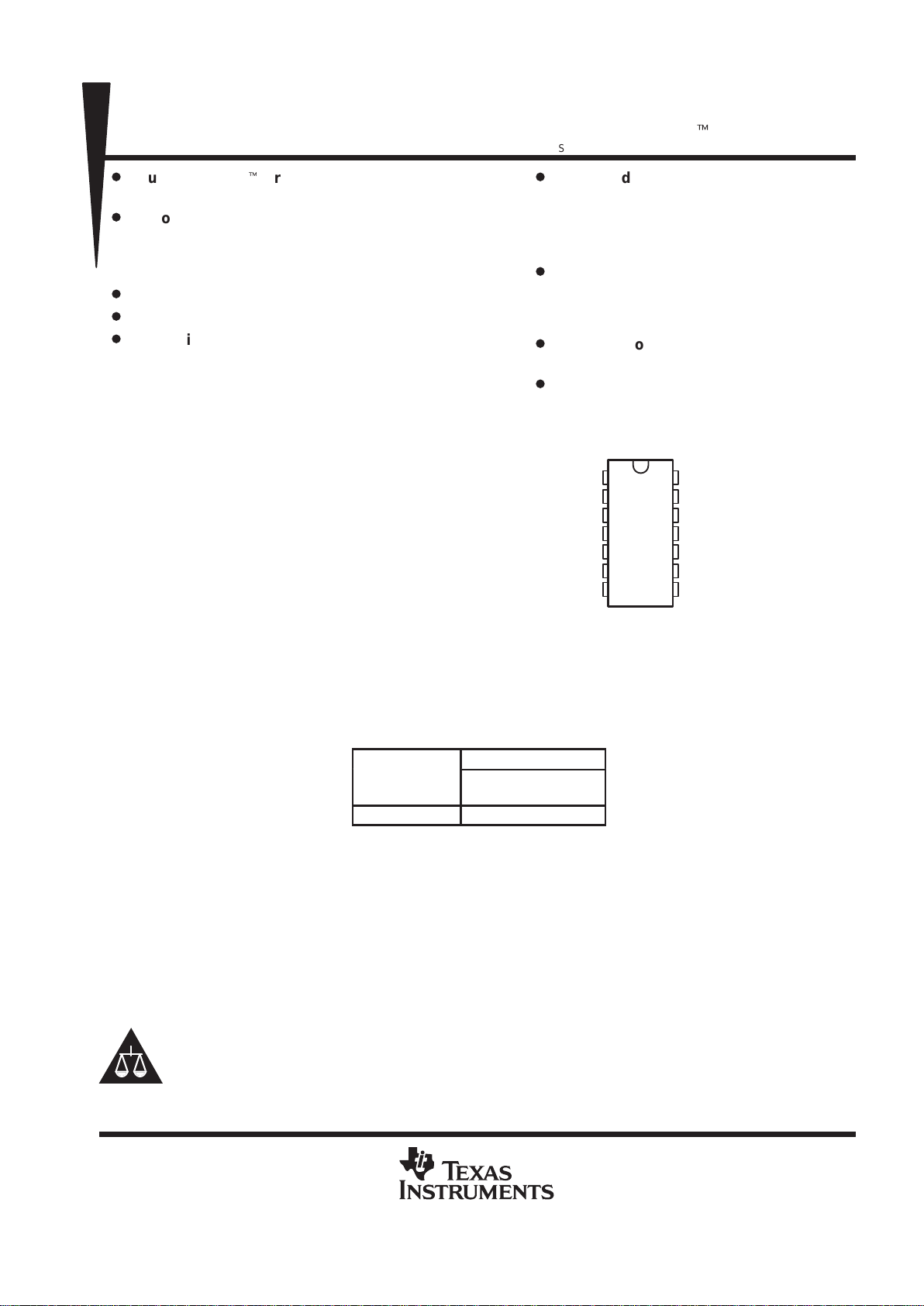
D PACKAGE
(TOP VIEW)
TLV5590
2-BIT ANALOG-TO-DIGITAL CONVERTER
FOR FLEXt PAGER CHIPSET
SLAS134B – NOVEMBER 1995 – REVISED NOVEMBER 1996
1
POST OFFICE BOX 655303 • DALLAS, TEXAS 75265
D
Supports FLEXt Protocol Pagers With The
TL V5591 FLEX Decoder
D
3-Pole Butterworth Low-Pass Selectable
Dual-Bandwidth Audio Filter
– BW 1 = 1 kHz ±5% (– 3 dB)
– BW 2 = 2 kHz ±5% (– 3 dB)
D
Both Peak and Valley Detectors Available
D
2-Bit Analog-to-Digital Converter
D
Operating Temperature Range...–25°C to 85°C
D
Four Modes of Operation:
– Fast Acquisition
– Slow Acquisition
– Hold Acquisition
– Standby
D
2.7-V to 3.3-V Single Power Supply
Operation
applications
D
FLEX Protocol Numeric and
Alphanumeric Pagers
D
One-Way or Two-Way
description
The TLV5590 analog-to-digital converter is a
system level solution to interface a 4-level
baseband audio signal to a digital decoder. The
TL V5590 is a direct interface to the TLV5591BVF
†
FLEX decoder. Designed primarily for pager
applications, the TLV5590 incorporates signal
conditioning, both peak and valley detection along
with analog-to-digital conversion. A selectable
third-order Butterworth filter with cutoff
frequencies of 1 kHz and 2 kHz is included. The
peak and valley detectors are implemented with a unique design that does not require external capacitors. Two
8-bit digital-to-analog converters (DACs) are used in a feedback loop to automatically adjust to the peak and
valley levels. The DAC outputs are used to set V
ref+
and V
ref–
for the 2-bit analog-to-digital converter (ADC).
Modes of operation include fast track, slow track, hold, and standby . The standby mode maximizes battery life.
The TLV5590 operates on a single supply down to 2.7 V.
AVAILABLE OPTIONS
PACKAGE
T
A
SMALL OUTLINE
(D)
–25°C to 85°C TLV5590ED
Please be aware that an important notice concerning availability, standard warranty, and use in critical applications of
Texas Instruments semiconductor products and disclaimers thereto appears at the end of this data sheet.
FLEX is a trademark of Motorola, Incorporated.
†
TLV5591BVF Data Manual Literature Number – SLWS048
PRODUCTION DATA information is current as of publication date.
Products conform to specifications per the terms of Texas Instruments
standard warranty. Production processing does not necessarily include
testing of all parameters.
Copyright 1996, Texas Instruments Incorporated
TLV5590
2-BIT ANALOG-TO-DIGITAL CONVERTER
FOR FLEXt PAGER CHIPSET
SLAS134B – NOVEMBER 1995 – REVISED NOVEMBER 1996
2
POST OFFICE BOX 655303 • DALLAS, TEXAS 75265
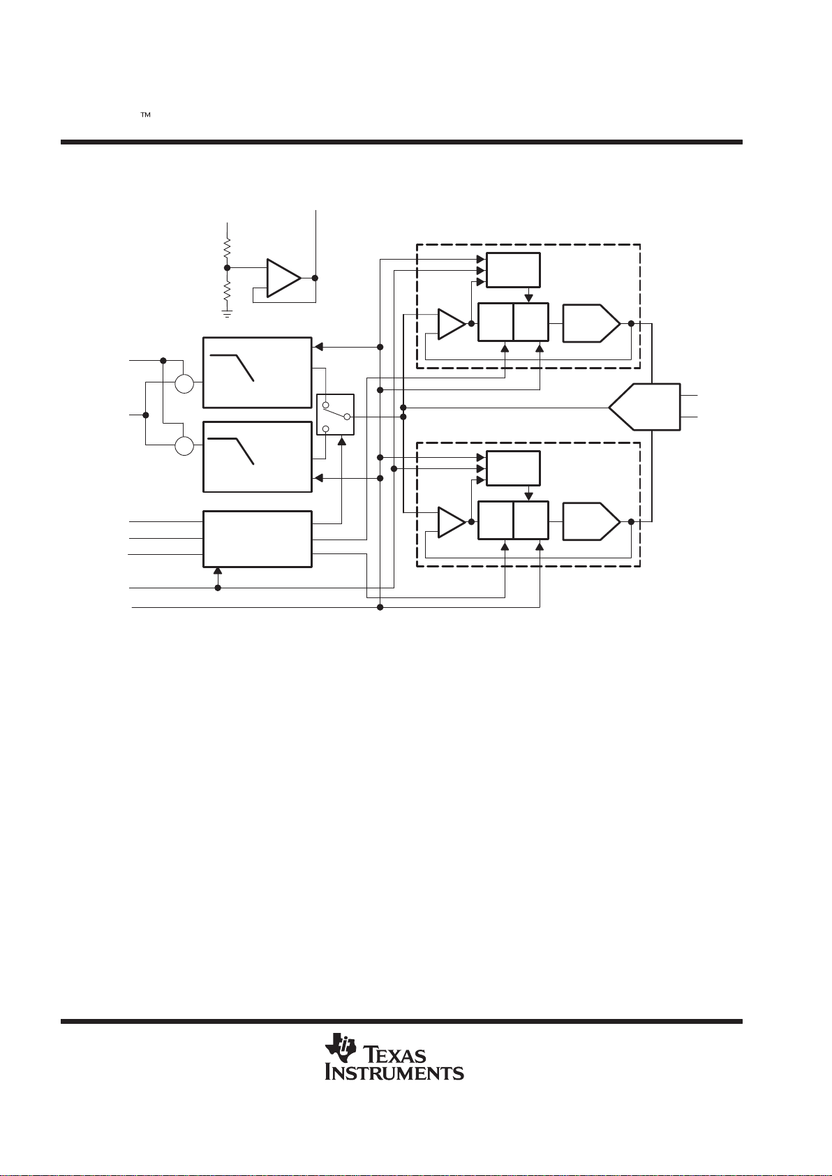
functional block diagram
_
+
8-Bit
DAC
CTR
2-Bit
ADC
fs = 1 kHz
Gain = 12
dB nom.
3rd-Order Butterworth
3rd-Order Butterworth
Mode Control
and Enable
AV
DD
MID
Peak Detector
Valley Detector
REF +
REF –
EXTS0
EXTS1
DC OFFSET
SIG
CON1
CON2
BW
TRACKINH
11
10
5
2
4
3
8
9
7
12
Up/
Down
CLK
14
fs = 2 kHz
Gain = 12
dB nom.
FILOUT
Σ
Σ
–
–
Decay
Counter
8-Bit
DAC
CTR
Up/
Down
Decay
Counter
TLV5590
2-BIT ANALOG-TO-DIGITAL CONVERTER
FOR FLEXt PAGER CHIPSET
SLAS134B – NOVEMBER 1995 – REVISED NOVEMBER 1996
3
POST OFFICE BOX 655303 • DALLAS, TEXAS 75265
Terminal Functions
TERMINAL
I/O
NAME NO.
DESCRIPTION
AV
DD
2 I Analog supply voltage
BW 7 I Digital bandwidth select. A high level on BW selects the 2-kHz filter cutoff and a low level selects the 1-kHz
filter cutoff.
CON1 8 I Digital control 1 input. In conjunction with CON2, CON1 selects the fast acquisition mode, slow acquisition
mode, hold or standby .
CON2 9 I Digital control 2 input. In conjunction with CON1, CON2 selects the fast acquisition mode, slow acquisition
mode, hold or standby .
CLK 14 I Digital clock input. CLK input is a 50% duty cycle TTL-level clock input with nominal frequency of 38.4 kHz.
The CLK input is edge sensitive in all non-test modes. For all test modes, the CLK input is level sensitive.
DC OFFSET 4 I Analog dc offset correction input. The dc component of the audio signal should be applied to DC OFFSET.
DV
DD
1 I Digital supply voltage
EXTS0 11 O Digital output 0 of the ADC. Data bit 0 is the LSB.
EXTS1 10 O Digital output 1 of the ADC. Data bit 1 is the MSB.
GND 6 Return terminal for the IC current.
SIG 3 I Analog audio signal input. An appropriate RC low-pass filter (antialiasing filter) should be connected to SIG.
MID 5 O Analog midpoint output. MID is a buffered output of AVDD/2.
TEST 13 I Digital test input enable. TEST should be connected to ground in normal operation.
TRACKINH 12 I Digital track inhibit logic input. A high level on TRACKINH disables the peak and valley detector counters, and
a low level enables the peak and valley detector counters. The counters continue to decay at the decay rate
while TRACKINH is a low level.
TLV5590
2-BIT ANALOG-TO-DIGITAL CONVERTER
FOR FLEXt PAGER CHIPSET
SLAS134B – NOVEMBER 1995 – REVISED NOVEMBER 1996
4
POST OFFICE BOX 655303 • DALLAS, TEXAS 75265
absolute maximum ratings over operating free-air temperature range (unless otherwise noted)
†
Supply voltage range, AV
DD
, DVDD –0.5 V to 6.5 V. . . . . . . . . . . . . . . . . . . . . . . . . . . . . . . . . . . . . . . . . . . . . . . . .
Input voltage range, V
I
–0.3 V to AV
DD
+ 0.3 V. . . . . . . . . . . . . . . . . . . . . . . . . . . . . . . . . . . . . . . . . . . . . . . . . . . . .
Output voltage range, EXTS0, EXTS1 –0.3 V to DV
DD
+ 0.3 V. . . . . . . . . . . . . . . . . . . . . . . . . . . . . . . . . . . . . . .
Offset input voltage, V
IO
–0.3 V to AV
DD
+ 0.3 V. . . . . . . . . . . . . . . . . . . . . . . . . . . . . . . . . . . . . . . . . . . . . . . . . . .
Peak input current (any input) ±20 mA. . . . . . . . . . . . . . . . . . . . . . . . . . . . . . . . . . . . . . . . . . . . . . . . . . . . . . . . . . . .
Operating free-air temperature range, T
A
–25°C to 85° C. . . . . . . . . . . . . . . . . . . . . . . . . . . . . . . . . . . . . . . . . . . .
Storage temperature range, T
stg
–65°C to 150° C. . . . . . . . . . . . . . . . . . . . . . . . . . . . . . . . . . . . . . . . . . . . . . . . . . .
Lead temperature 1,6 mm (1/16 inch) from case for 10 seconds 260°C. . . . . . . . . . . . . . . . . . . . . . . . . . . . . . .
†
Stresses beyond those listed under “absolute maximum ratings” may cause permanent damage to the device. These are stress ratings only, and
functional operation of the device at these or any other conditions beyond those indicated under “recommended operating conditions” is not
implied. Exposure to absolute-maximum-rated conditions for extended periods may affect device reliability.
recommended operating conditions
MIN NOM MAX UNIT
Supply voltage, AVDD, DV
DD
2.7 3.3 V
Power supply ripple 0.002 V
pp
Input clock frequency, f
(CLK)
38.4 kHz
Input clock duty cycle 45 50 55 %
Voltage of fset applied at DC OFFSET, V
I(DC OFFSET)
(see Notes 1 and 2) 0.25 VDD–0.25 V
Analog input voltage, V
I(pp)
(See Notes 1 and 2) VDD = 3.1 V 0.25 VDD – 0.25 V
pp
High-level control input voltage, V
IH
VDD = 2.7 V to 3.3 V 0.2 DV
DD
V
Low-level control input voltage, V
IL
VDD = 2.7 V to 3.3 V 0.8 DV
DD
V
Operating free-air temperature, T
A
–25 85 °C
NOTES: 1. V
I(OFFSET)
=VQ – V
I(DC OFFSET)
where VQ is the dc quiescent voltage of the signal applied to the SIG terminal.
NOTES: 2.
V
I(PEAK)
+
ǒ
V
DD
2
*
0.25 V
Ǔ
4.217
*
V
I
(OFFSET)*80 mV
The pass-band filter gain represents the maximum specified voltage gain in volts/volt of the filter. The maximum gain for the filter
is 4.217 V/V (12.5 dB). The input voltage range from this equation defines the maximum allowable input signal at the SIG terminal
with a given voltage, V
I(DC OFFSET)
, applied at the DC OFFSET terminal and a quiescent dc input voltage, VQ, of the signal applied
at the SIG terminal. When the input voltage is within this range, the peak and valley DACs do not over range. The 80 mV value is
the tolerance on the voltage output at the MID terminal.
TLV5590
2-BIT ANALOG-TO-DIGITAL CONVERTER
FOR FLEXt PAGER CHIPSET
SLAS134B – NOVEMBER 1995 – REVISED NOVEMBER 1996
5
POST OFFICE BOX 655303 • DALLAS, TEXAS 75265
electrical characteristics over recommended operating free-air temperature range,
AV
DD
= DV
DD
= 2.7 V to 3.3 V, f
(CLK)
= 38.4 kHz (unless otherwise noted)
power
PARAMETER TEST CONDITIONS MIN MAX UNIT
I
DD
Operating supply current Fast track, slow track, or hold mode 250 µA
I
DD(standby)
Standby supply current
V
I(DC OFFSET)
= 0.8 V,
V
I(SIG)
= 0.8 V , For all digital inputs,
0 < VI < 0.5 V or VI > DVDD –0.5 V
1 µA
digital
PARAMETER TEST CONDITIONS MIN TYP MAX UNIT
V
OH
High-level output voltage IOH = –100 µA DVDD –0.5 V
V
OL
Low-level output voltage IOL = 100 µA 0.5 V
I
IH
High-level input current VI = DV
DD
0.1 1 µA
I
IL
Low-level input current VI = 0 –0.1 –1 µA
C
i
Input capacitance, digital input 10 pF
analog
PARAMETER TEST CONDITIONS MIN TYP MAX UNIT
Voltage accuracy at MID VDD = 3 V, C
L(MID)
= 220 nF 1.42 1.5 1.58 V
Z
i
Input impedance at SIG (see Note 3) f
(IN)
= 800 Hz 1 MΩ
Z
i(offset)
Input impedance at DC OFFSET (see Note 3) 1 3 MΩ
I
I(SIG)
Average input current into SIG GND < VI < AV
DD
50 200 nA
C
i
Input capacitance, analog input at SIG 10 pF
NOTE 3: The input is capacitive and, therefore, is dynamic. Impedance specifications are based on f
(CLK)
= 38.4 kHz.
operating characteristics over recommended operating free-air temperature range,
AV
DD
=DVDD=3 V, f
(CLK)
= 38.4 kHz (unless otherwise noted)
peak-and-valley DACs
PARAMETER TEST CONDITIONS MIN TYP MAX UNIT
Step size, LSB VDD/255 V
E
FS
Full-scale error ±1 LSB
E
ZS
Zero-code error ±3 LSB
Voltage output drift Hold mode 0 mV/ms
E
D
Differential linearity error ±1 LSB
low-pass filter
PARAMETER TEST CONDITIONS MIN TYP MAX UNIT
G Pass band filter gain V
I(DC OFFSET)
= 0.8 V, VI = ± 125 mV 1 1.5 12 12.5 dB
1-kHz filter VI = ± 500 mV f
I(SIG)
= 1 kHz 2 3 4
Filter attenuation
2-kHz filter VI = ± 500 mV f
I(SIG)
= 2 kHz 2 3 4
dB
t
s
Stabilization time Off mode to hold mode (see Table 1) 5 ms

TLV5590
2-BIT ANALOG-TO-DIGITAL CONVERTER
FOR FLEXt PAGER CHIPSET
SLAS134B – NOVEMBER 1995 – REVISED NOVEMBER 1996
6
POST OFFICE BOX 655303 • DALLAS, TEXAS 75265
PARAMETER MEASUREMENT INFORMATION
Value A Value B
Based on Value A Based on Value B
CLK
TRACKINH
(external)
TRACKINH
(internal)
Peak/Valley
Counter Value
EXTS0, EXTS1
Outputs
See Note A
NOTE A: Internally the device recognizes input conditions on the falling edge of the clock only.
Figure 1. Timing Diagram
CLK
CON1
CON2
TRACKINH
NOTES: A. Internally the device recognizes input conditions on the falling edge of the clock only.
B. On the next falling edge of the clock with the input conditions shown, the TLV5590 tracks signal in fast mode (peak DAC counter
counts down by 8 and up by 4) in time A.
C. On the next falling edge of the clock with the input conditions shown, the TLV5590 tracks signal in slow mode (peak DAC counter
counts up by 2 and down by 1 every 40 clock cycles) in time B.
D. On the next falling edge of the clock with the input conditions shown, the TLV5590 holds previous peak and valley levels in time
C. For the 2 bit ADC, when TRACKINH = 1, EXTS0 and EXTS1 outputs respond in real time to the condition of SIG and DC
OFFSET as long as the CLK signal is present.
See Note B See Note C See Note DTime A Time B Time C
See Note A
Figure 2. Track and Lock Timing

TLV5590
2-BIT ANALOG-TO-DIGITAL CONVERTER
FOR FLEXt PAGER CHIPSET
SLAS134B – NOVEMBER 1995 – REVISED NOVEMBER 1996
7
POST OFFICE BOX 655303 • DALLAS, TEXAS 75265
TYPICAL CHARACTERISTICS
Figure 3
–6
–15
–21
–30
31.25 62.5 125 250 500 1 k
G – Nominal Gain – dB
0
9
f – Frequency – Hz
NOMINAL FILTER GAIN
vs
FREQUENCY
15
2 k 4 k 8 k
12
6
3
–3
–9
–12
–18
–24
–27
1 kHz Filter Response
Figure 4
–6
–15
–21
–30
62.5 125 250 500 1 k
G – Nominal Gain – dB
0
9
f – Frequency – Hz
NOMINAL FILTER GAIN
vs
FREQUENCY
15
2 k 4 k 8 k
12
6
3
–3
–9
–12
–18
–24
–27
2 kHz Filter Response
16 k

TLV5590
2-BIT ANALOG-TO-DIGITAL CONVERTER
FOR FLEXt PAGER CHIPSET
SLAS134B – NOVEMBER 1995 – REVISED NOVEMBER 1996
8
POST OFFICE BOX 655303 • DALLAS, TEXAS 75265
PRINCIPLES OF OPERATION
analog input operation
Referring to the functional block diagram, the signal input is dc-coupled using a single input terminal, SIG. The
nominal dc content of the signal input should be supplied on an additional terminal, DC OFFSET. This allows
the device to gain the signal to acceptable levels for threshold detection, without saturating against the supplies.
The signal processed by the device is effectively the voltage difference between the SIG and DC OFFSET
terminals.
There is no antialiasing filter incorporated in the device and it is recommended that this filtering be added
externally by an external RC filter set at the appropriate cutoff (see Figure 5).
The maximum peak analog-signal voltage that can be applied to the SIG input terminal is given by:
V
I(PEAK)
+
ǒ
V
DD
2
*
0.25
Ǔ
4.217
*
V
I(OFFSET)
–80mV
where
V
DD
ń
2+the nominal output voltage at the MID terminal
VQ+
the dc quiescent voltage of the input signal
V
I(DC OFFSET)
+
the voltage applied to the DC OFFSET terminal
and
V
I(OFFSET)
+
VQ*
V
I(DC OFFSET)
The value of 80 mV is the tolerance of the output voltage for the MID terminal at the output of the internal filter
amplifier.
The peak-to-peak input voltage swing is double the result shown in the equation.
The main signal path consists of a third-order switched-capacitor butterworth filter, with a switchable bandwidth
between 1 kHz and 2 kHz, to remove the noise from the input signal. The peak and valley amplitudes of the filter
output signal are detected and subsequently used to convert the 4-level audio into 2-level digital signals using
three switched capacitor comparators.
digital operation
The peak and valley detection is performed by a mixed mode solution, using an 8-bit DAC and an up/down
counter that has nonsymmetrical up and down count rates. V arious modes are included to force the peak and
valley circuits to slow track, fast track, or hold. An off mode is included that forces the device into a low-power
condition. The decay rate of the peak and valley circuits are controlled by independent counters.
The device is clocked with a 38.4 kHz square wave supplied externally . The attack and decay times of the peak
and valley circuits, and the filter cut-off frequencies are directly related to this clock frequency . The decay timer
is gated by the track inhibit input TRACKINH, and is reset to 1 after an attack occurs, and is reset to 40 after
a decay enable. The TRACKINH also prevents attack enable inputs from affecting the peak and valley counters.

TLV5590
2-BIT ANALOG-TO-DIGITAL CONVERTER
FOR FLEXt PAGER CHIPSET
SLAS134B – NOVEMBER 1995 – REVISED NOVEMBER 1996
9
POST OFFICE BOX 655303 • DALLAS, TEXAS 75265
PRINCIPLES OF OPERATION
digital control
There are five digital inputs that control the TL V5590, along with the CLK input. The five signals are BW, CON1,
CON2, TRACKINH and TEST . All digital control inputs are latched internally on the falling edge of the CLK input.
The BW input selects the cut-off frequency of the input signal third-order Butterworth switched-capacitor filter .
The CON1 and CON2 inputs determine when the TL V5590 is in tracking fast, tracking slow , hold, or low-power
standby mode. In test mode the CLK input is level sensitive, and in all other modes the CLK input is
edge-sensitive.
Table 1 lists the functions for the five control inputs.
Table 1. Control Inputs Function Table
BW
SWITCHED-CAPACITOR FILTER
(– 3 dB POINT)
Low 1-kHz filter cutoff
High 2-kHz filter cutoff
CON1 CON2 MODE
Low Low Low-power standby (off) mode
Low High Fast track mode
High Low Hold mode
High High Slow track mode
TRACKINH RESULT
Low Tracking enabled
High Tracking disabled
track inhibit
The TRACKINH input enables the counters to the peak and valley detector DACs. When enabled, the counters
are adjusting to create a DAC output that is the same as the filtered input-signal peak and valley . The counters
decay at the fast or slow decay rates while the TRACKINH input is held low. The TRACKINH line should be
connected to SYMCLK terminal on the TLV5591.
analog-to-digital conversion
The TLV5590 employs a 2-bit ADC to convert a 4-level analog signal to digital data. The digital output is
presented on EXTS0 and EXTS1 with EXTS0 being the LSB. The peak and valley DACs provide the maximum
and minimum voltages (V
ref+
and V
ref–
) to the ADC. The input to the 2-bit ADC is the output of the Butterworth
low-pass filter, FILOUT, as shown in the block diagram. The ADC transfer function is shown in Table 2.
Table 2. Filter Output Voltage Selection (see Note 4)
EXTS1 EXTS0 FILTER OUTPUT VOLTAGE (FILOUT)
Low Low FILOUT < ((peak – valley) x 50/256) + valley
High Low ((peak – valley) x 50/256) + valley < FILOUT < ((peak – valley) x 134/256) + valley
High High ((peak – valley) x 134/256) + valley < FILOUT < (( peak – valley) x 217/256) + valley
Low High FILOUT > ((peak – valley) x 217/256) + valley
NOTE 4. The constants 50/256, 134/256, and 217/256 have a± 5% tolerance.

TLV5590
2-BIT ANALOG-TO-DIGITAL CONVERTER
FOR FLEXt PAGER CHIPSET
SLAS134B – NOVEMBER 1995 – REVISED NOVEMBER 1996
10
POST OFFICE BOX 655303 • DALLAS, TEXAS 75265
PRINCIPLES OF OPERATION
The thresholds for the ADC comparators are set by capacitor ratios in switched-capacitor comparators. For a
2-bit ADC, three comparators are used with thresholds set as shown in Table 3.
Table 3. Comparators and Associated Threshold Values (see Notes 4 and 5)
COMPARATOR VALUE UNIT
Lower threshold ((peak – valley) x 50/256) + valley V
Middle threshold ((peak – valley) x 134/256) + valley V
Upper threshold ((peak – valley) x 217/256) + valley V
NOTES: 4. The constants 50/256, 134/256, and 217/256 have a ± 5% tolerance.
5. The comparator thresholds are measured with the input voltage level of the SIG terminal at 125 mV ac
centered on 800 mV dc and the input voltage at the DC OFFSET terminal is 800 mV dc.
peak and valley timing
The peak and valley attack and delay times are controlled by two 8-bit up/down counters clocked by the CLK
input. The rate that the counters are clocked depends on whether the counters are in attack or decay mode.
The peak counter is in attack mode when the input signal amplitude is greater than the output voltage from the
peak DAC, and it is in decay mode when the input signal amplitude is less that the peak DAC output voltage.
The valley counter is in attack mode when the input signal amplitude is less than the output voltage from the
valley DAC, and it is in decay mode when the input signal amplitude is greater than the valley DAC output
voltage.
When TRACKINH is held high, the attack and decay enable inputs to the peak and valley counters are disabled.
When held low the attack and decay enable inputs to the peak and valley counters are enabled. The effect of
the TRACKINH signal is exactly the same as when the device is configured in hold mode.
slow-acquisition-mode attack and decay times
The attack rate is calculated equal to [V
DD
×f
(CLK)
×2] / 256 / (TRACKINH duty cycle). So the peak and valley
counter is incremented/decremented by a count of 2 on every clock cycle when the input signal amplitude is
greater or less than the peak and valley DAC output voltage.
The decay rate is calculated equal to [V
DD
×f
(CLK)
] / (256 ×40) / (TRACKINH duty cycle). So the peak and valley
counter is decremented or incremented once every 40 clock cycles when the input signal amplitude is less or
greater than the peak and valley DAC output voltage.
When the counters receive an attack enable at the same time as a decay enable then the attack enable takes
precedence. The decay counter is reset to 1 after an attack and reset to 40 following a decay.
With a V
DD
supply variation of 2.7 V to 3.3 V, and a fixed clock input of 38.4 kHz, the attack and decay times
are given in Table 4.
Table 4. Slow Acquisition Mode Attack and Decay Times
DESCRIPTION CONDITIONS MIN MAX UNIT
Attack Rate (ATTR) TRACKINH = Low 810 990 mV/ms
Decay Rate (DECR) TRACKINH = Low 10.125 12.375 mV/ms

TLV5590
2-BIT ANALOG-TO-DIGITAL CONVERTER
FOR FLEXt PAGER CHIPSET
SLAS134B – NOVEMBER 1995 – REVISED NOVEMBER 1996
11
POST OFFICE BOX 655303 • DALLAS, TEXAS 75265
PRINCIPLES OF OPERATION
fast-acquisition-mode attack and decay times
The attack rate is calculated equal to [V
DD
×f
(CLK)
×4] / 256 / (TRACKINH duty cycle). So the peak and valley
counter is incremented or decremented by a count of 4 on every clock cycle when the input signal amplitude
is greater or less than the peak and valley DAC output voltage.
The decay rate is calculated equal to [V
DD
×f
(CLK)
×8] / 256 / (TRACKINH duty cycle). So the peak and valley
counter is decrement or increment by a count of 8 on every clock cycle when the input signal amplitude is less
or greater than the peak and valley DAC output voltage.
When the device is in fast aquistion mode then the decay counter is reset to 1.
With a V
DD
supply variation of 2.7 V to 3.3 V, and a fixed clock input of 38.4 kHz, the attack and decay times
are given in Table 5.
Table 5. Fast Acquisition Mode Attack and Decay Times
DESCRIPTION CONDITIONS MIN MAX UNIT
Attack Rate (ATTR) TRACKINH = Low 1620 1980 mV/ms
Decay Rate (DECR) TRACKINH = Low 3240 3960 mV/ms
hold mode
In hold mode the peak and valley counters are disabled from counting when either attack or decay enable
signals are present. There is no change to the peak and valley DAC output voltages in this mode.
When the device is in hold mode then the decay counter is reset to 1.
off mode
In the off mode the peak and valley counters are disabled from counting, and the device is set into low power
standby mode. The peak and valley voltages both float to the V
DD
voltage as the resistor string element within
the DAC structure is isolated from the GND supply to conserve power. When the of f state is released the peak
and valley voltages return to the previously set values.
When the device is in off mode then the decay counter is reset to 1.
test
The TEST input allows access to internal circuitry for production testing purposes and the pager system debug.
For normal operation, TEST should be tied to ground. For the debug and test mode, the TEST input should be
held high. The various operating modes are described in the following sections.

TLV5590
2-BIT ANALOG-TO-DIGITAL CONVERTER
FOR FLEXt PAGER CHIPSET
SLAS134B – NOVEMBER 1995 – REVISED NOVEMBER 1996
12
POST OFFICE BOX 655303 • DALLAS, TEXAS 75265
PRINCIPLES OF OPERATION
test mode 0 – peak and valley DACs and logic testing
Test mode 0 can be used for production testing and allows complete testing of the peak and valley DAC
counters, decay counters, and the peak and valley DACs. The peak and valley DAC voltage outputs are
accessible on the EXTS1 and EXTS0 terminals respectively , and the decay rate-counter outputs are accessible
on the SIG terminal. The DAC counters are controlled by the various digital inputs. The BW input controls the
counter reset, and the TRACKINH input controls the peak and valley DAC counters up and down control, and
multiplexes the decay rate-counter outputs onto the SIG terminal. The DC OFFSET input selects the counters
fast and slow modes of operation. The counters are enabled and are clocked on each rising edge of the CLK
input. Table 6 contains a terminal function summary of this test mode.
Table 6. Test Mode 0 Selection
TEST = HIGH, CON1 = LOW, CON2 = LOW
TEST INPUTS
TERMINAL INPUT RESULT / MODE
Low Logic enabled
BW
High Logic reset
Low Peak and valley counters count down, valley-decay counter output on SIG terminal.
TRACKINH
High Peak and valley counters count up, peak decay-counter output on SIG terminal.
Low
Device taken from fast mode to test mode 0:
a) Peak counter counts in slow mode
b) Valley counter counts in fast mode
Device taken from slow mode to test mode 0, and the peak and valley counters
count in slow mode.
DC OFFSET
High
Device taken from fast mode to test mode 0:
a) Peak counter counts in fast mode
b) Valley counter counts in slow mode
g
Device taken from slow mode to test mode 0, and the peak and valley counters
count in fast mode.
TEST OUTPUTS
TERMINAL CONDITIONS RESULT / MODE
EXTS1 Peak DAC voltage
EXTS0 Valley DAC voltage
TRACKINH = Low Valley-decay counter output
SIG
†
TRACKINH = High Peak-decay counter output
†
This function is valid when transitioning from slow mode to the test mode 0. In fast mode, the DC OFFSET terminal function is inverted
for the valley counter only.

TLV5590
2-BIT ANALOG-TO-DIGITAL CONVERTER
FOR FLEXt PAGER CHIPSET
SLAS134B – NOVEMBER 1995 – REVISED NOVEMBER 1996
13
POST OFFICE BOX 655303 • DALLAS, TEXAS 75265
PRINCIPLES OF OPERATION
test mode 1 – switched-capacitor filter test
Test mode 1 places the output of the switched-capacitor low-pass filter directly on EXTS1. Note that the filter
output is not capable of driving an external load and, therefore, must be buffered externally at the EXTS1
terminal of the TL V5590. The BW input selects the filter cut-off frequency. The peak and valley DAC counters,
the decay counters, and the 2-bit ADC are all disabled during this test mode. T able 7 contains a terminal function
summary of this test mode.
Table 7. Test Mode 1 Selection
TEST = HIGH, CON1 = LOW, CON2 = HIGH
TEST INPUT
TERMINAL INPUT RESULT/MODE
Low 1-kHz cutoff frequency (–3 dB)
BW
High 2-kHz cutoff frequency (–3 dB)
TEST OUTPUT
TERMINAL OUTPUT SIGNAL
EXTS1 Switched-capacitor filter output (unbuffered)
†
†
The filter output must be buffered externally for testing.
test mode 2 – peak and valley DAC output test
Test mode 2 allows direct access to the peak and valley comparators and can be used for the pager system
debug. The peak and valley comparator outputs are accessible on the EXTS0 and EXTS1 terminals
respectively . The peak and valley counters are held at a constant value using the hold mode. Table 8 contains
a terminal function summary of this test mode.
Table 8. Test Mode 2 Selection
TEST = HIGH, CON1 = HIGH, CON2 = LOW
TEST OUTPUTS
TERMINAL OUTPUT SIGNAL
EXTS1 Peak DAC voltage
EXTS2 Valley DAC voltage

TLV5590
2-BIT ANALOG-TO-DIGITAL CONVERTER
FOR FLEXt PAGER CHIPSET
SLAS134B – NOVEMBER 1995 – REVISED NOVEMBER 1996
14
POST OFFICE BOX 655303 • DALLAS, TEXAS 75265
PRINCIPLES OF OPERATION
test mode 3 – comparator threshold test
Test mode 3 allows a dc input voltage to be applied to force the peak and valley DAC voltages to settle
independently at their nominal output voltages including any effects of the filter dc offsets, gain errors, etc. The
input signal can then be set at the comparator switching thresholds and the correct outputs should be decoded.
The normal outputs of the ADC are present on EXTS0 and EXTS1. The BW and TRACKINH inputs override
the peak and valley DAC counter disables. The switched-capacitor filter is forced into a 1-kHz cut-off mode.
Table 9 contains a terminal function summary of this test mode.
Table 9. Test Mode 3 Selection
TEST = HIGH, CON1 = HIGH, CON2 = HIGH
TEST INPUTS
TERMINAL INPUT RESULT
Low Peak DAC counter normal operation
BW
High Peak DAC counter disabled
Low Valley DAC counter normal operation
TRACKINH
High Valley DAC counter disabled

TLV5590
2-BIT ANALOG-TO-DIGITAL CONVERTER
FOR FLEXt PAGER CHIPSET
SLAS134B – NOVEMBER 1995 – REVISED NOVEMBER 1996
15
POST OFFICE BOX 655303 • DALLAS, TEXAS 75265
APPLICATION INFORMATION
The TLV5590 is optimized for pager applications. The TL V5590 optimizes the filtering and conversion resolution
to meet the specific requirements of FLEX pagers. The combination of the TL V5590 and TLV5591 reduce overall
system cost by allowing a lower cost microcontroller to be used in the pager system. Figure 5 shows the basic
connections between system elements.
SIG
0.1 µF
TLV5591
FLEX
Decoder
2.7 V
Microcontroller
Receiver
AV
DD
DV
DD
EXTS0
EXTS1
TRACKINH
CON2
TLV5590
CON1
BW
CLK
SDI
SDO
SCK
TEST
GND
READY
SCK
MOSI
MISO
RESET
PORT
IRQ
EXTS0
EXTS1
SYMCLK
S5
S6
S4
CLKOUT
S0
0.0018 µF
18 KΩ
DC OFFSET
‡
MID
†
†
The voltage on the MID terminal is nominally AVDD/2.
‡
The voltage applied to the DC OFFSET terminal is set to the dc offset voltage of the input signal applied to the SIG terminal.
220 nF
Figure 5. TL V5590 Application Schematic
At least one bit of warm-up time in fast track mode followed by five bits of warm-up time in slow track mode is
necessary before valid data can be present. Hold mode is used during a data transfer, and fast track mode is
used for warm-up. Slow track mode is used for tracking during the synchronization portion of the data.

IMPORTANT NOTICE
T exas Instruments and its subsidiaries (TI) reserve the right to make changes to their products or to discontinue
any product or service without notice, and advise customers to obtain the latest version of relevant information
to verify, before placing orders, that information being relied on is current and complete. All products are sold
subject to the terms and conditions of sale supplied at the time of order acknowledgement, including those
pertaining to warranty, patent infringement, and limitation of liability.
TI warrants performance of its semiconductor products to the specifications applicable at the time of sale in
accordance with TI’s standard warranty. Testing and other quality control techniques are utilized to the extent
TI deems necessary to support this warranty. Specific testing of all parameters of each device is not necessarily
performed, except those mandated by government requirements.
CERT AIN APPLICATIONS USING SEMICONDUCTOR PRODUCTS MAY INVOLVE POTENTIAL RISKS OF
DEATH, PERSONAL INJURY, OR SEVERE PROPERTY OR ENVIRONMENTAL DAMAGE (“CRITICAL
APPLICATIONS”). TI SEMICONDUCTOR PRODUCTS ARE NOT DESIGNED, AUTHORIZED, OR
WARRANTED TO BE SUITABLE FOR USE IN LIFE-SUPPORT DEVICES OR SYSTEMS OR OTHER
CRITICAL APPLICATIONS. INCLUSION OF TI PRODUCTS IN SUCH APPLICA TIONS IS UNDERST OOD TO
BE FULLY AT THE CUSTOMER’S RISK.
In order to minimize risks associated with the customer’s applications, adequate design and operating
safeguards must be provided by the customer to minimize inherent or procedural hazards.
TI assumes no liability for applications assistance or customer product design. TI does not warrant or represent
that any license, either express or implied, is granted under any patent right, copyright, mask work right, or other
intellectual property right of TI covering or relating to any combination, machine, or process in which such
semiconductor products or services might be or are used. TI’s publication of information regarding any third
party’s products or services does not constitute TI’s approval, warranty or endorsement thereof.
Copyright 1998, Texas Instruments Incorporated
 Loading...