

D
General-Purpose Analog Interface Circuit
for VDSL System
D
12 Bit, 22 MHz ADC and DAC
D
Provides 11 MHz Bandwidth Performance
D
Supports Central Office and Remote
Terminal Applications
D
Excellent Power Management by
Enabling/Disabling Major Functional
Blocks When in Power Control Mode
D
Remote Activation Feature With Selectable
Wake-Up Tone Frequency
D
Integrated Equalizer to Partially
Compensate for the Roll Off in Twisted Pair
Telephone Cable
D
Numerically Controlled Oscillator With
Resolution <1 ppm, Range of 250 ppm
Using External Crystal
description
TLV320VD30
VDSL CODEC
SLWS086 – JUNE 1999
D
26 dB RFI Suppression
D
Programmable Receive Amplifier Operating
From 0 dB to 20 dB, in Steps of 1 dB
D
Programmable T ransmitter Output Power
Level From –13 dBm to 11 dBm
D
Enable/Disable of All Major Blocks During
Power Mode
D
Digital Loopback Test Mode
D
Internal Voltage References
D
Serial Control Port
D
Conversion Rate up to 22.08 MHz
D
Selectable Offset Binary or 2s Complement
Data Format
D
3.3 V Operation
D
80-Pin PN Package
The TLV320VD30 is an analog front end (AFE) device for VDSL systems. The TLV320VD30 provides a
transmitter and a receiver. Both the transmitter and receiver have up to 11 MHz-bandwidth performance. The
device can be used for central office and remote VDSL applications. The transmitter consists of a 12-bit/22 MHz
DAC and a programmable line driver interface. The receiver consists of a 12-bit/22 MHz ADC, a programmable
gain amplifier, a compromise equalizer , and an RFI cancellation circuit. The device includes a tone detect circuit,
and a numerically controlled crystal oscillator.
The TLV320VD30 provides two parallel ports for fast data transfers and a serial port for device control. The
parallel ports are 12-pin ports with data transfer rates of up to 22 MHz per 12-bit word. One parallel port is
dedicated to DAC input, the other parallel port is dedicated to ADC output. The serial port supports both write
and read operations. The serial data transfer rate is 1.38 MHz per bit. Data is transferred in 16-bit words.
Please be aware that an important notice concerning availability, standard warranty, and use in critical applications of
Texas Instruments semiconductor products and disclaimers thereto appears at the end of this data sheet.
PRODUCTION DATA information is current as of publication date.
Products conform to specifications per the terms of Texas Instruments
standard warranty. Production processing does not necessarily include
testing of all parameters.
POST OFFICE BOX 655303 • DALLAS, TEXAS 75265
Copyright 1999, Texas Instruments Incorporated
1
TLV320VD30
VDSL CODEC
SLWS086 – JUNE 1999
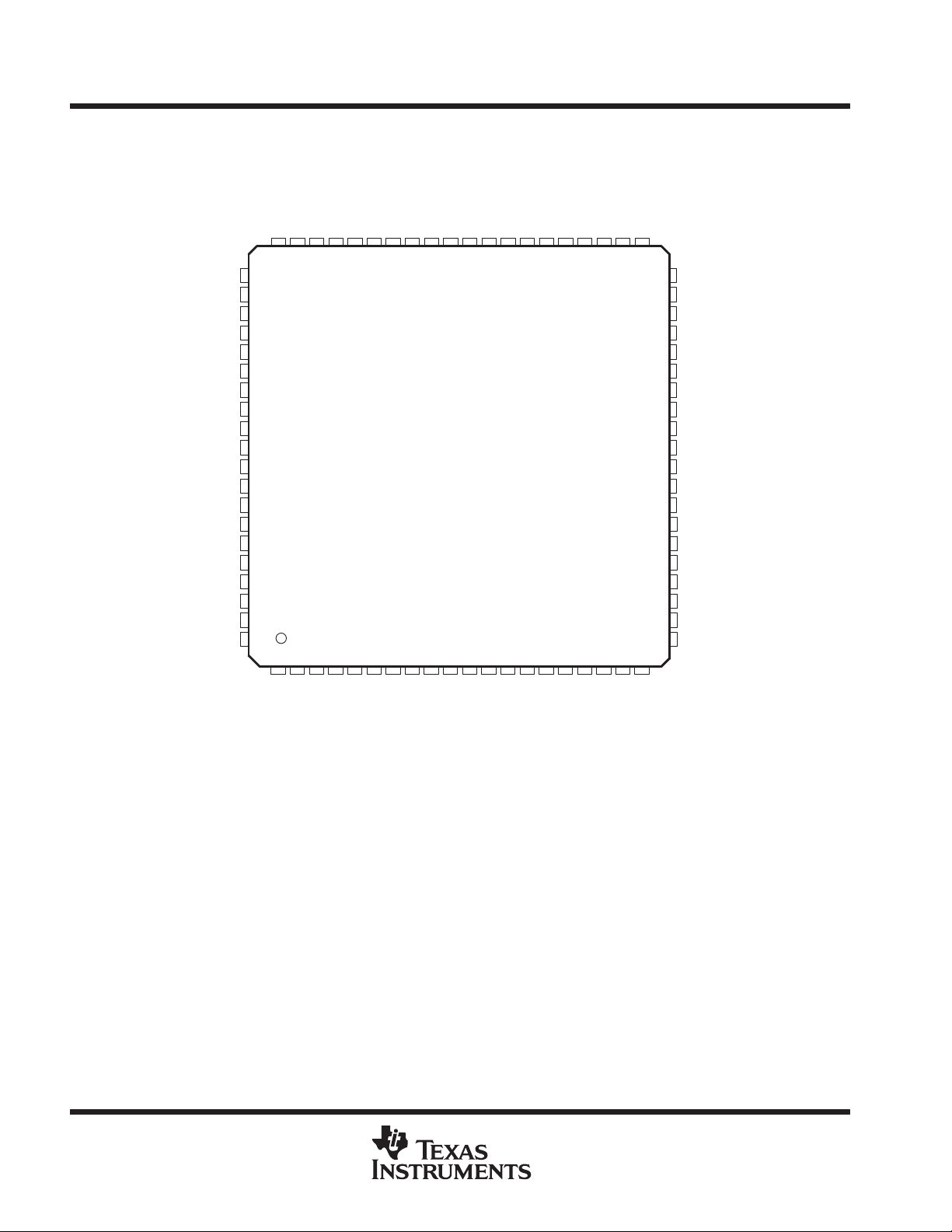
PN PACKAGE
(TOP VIEW)
VBG
AGND4
AVDD4
XIN
XOUT
CLKIN
EXTCLKEN
RESET
TEST3
RFIADAPTEN
TXENABLE
RXENABLE
SENABLE
SIN
DVDD
DGND
DAC<11>
DAC<10>
DAC<9>
DAC<8>
RSET
GUARDGND
59 58 57 56 5560 54
61
62
63
64
65
66
67
68
69
70
71
72
73
74
75
76
77
78
79
80
23
1
GUARDVDD
A VDD3
AGND3
SENSETXP
5678
4
A VDD2
RXP
RXM
49 48
TXP
TXBIASP
52 51 5053
TL V320VD30PN
10 11 12 13
9
TXBIASM
AGND2
47 46 45 44
14 15 16 17
TXM
SENSETXM
TDVREFM
TDVREFP
TESTM
VCM
43 42 41
18 19 20
TESTP
VCMSENSEM
40
VCMSENSEP
39
TESTCLK
38
AGND1
37
AVDD1
36
ADCGNDREF
35
NC
34
ADCGND
33
ADCVDD
32
GUARDGND
31
GUARDVDD
30
TONEDETECT
29
DGNDIO
28
DVDDIO
27
ADC<11>
26
ADC<10>
25
ADC<9>
24
ADC<8>
23
ADC<7>
22
ADC<6>
21
DAC<7>
DAC<6>
NC – No internal connection
DAC<5>
DAC<4>
DAC<3>
DAC<2>
DAC<1>
DAC<0>
CLK
DVDDIO
DGNDIO
SCLK
SOUT
ADC<0>
ADC<1>
SREADY
ADC<3>
ADC<4>
ADC<2>
ADC<5>
2
POST OFFICE BOX 655303 • DALLAS, TEXAS 75265
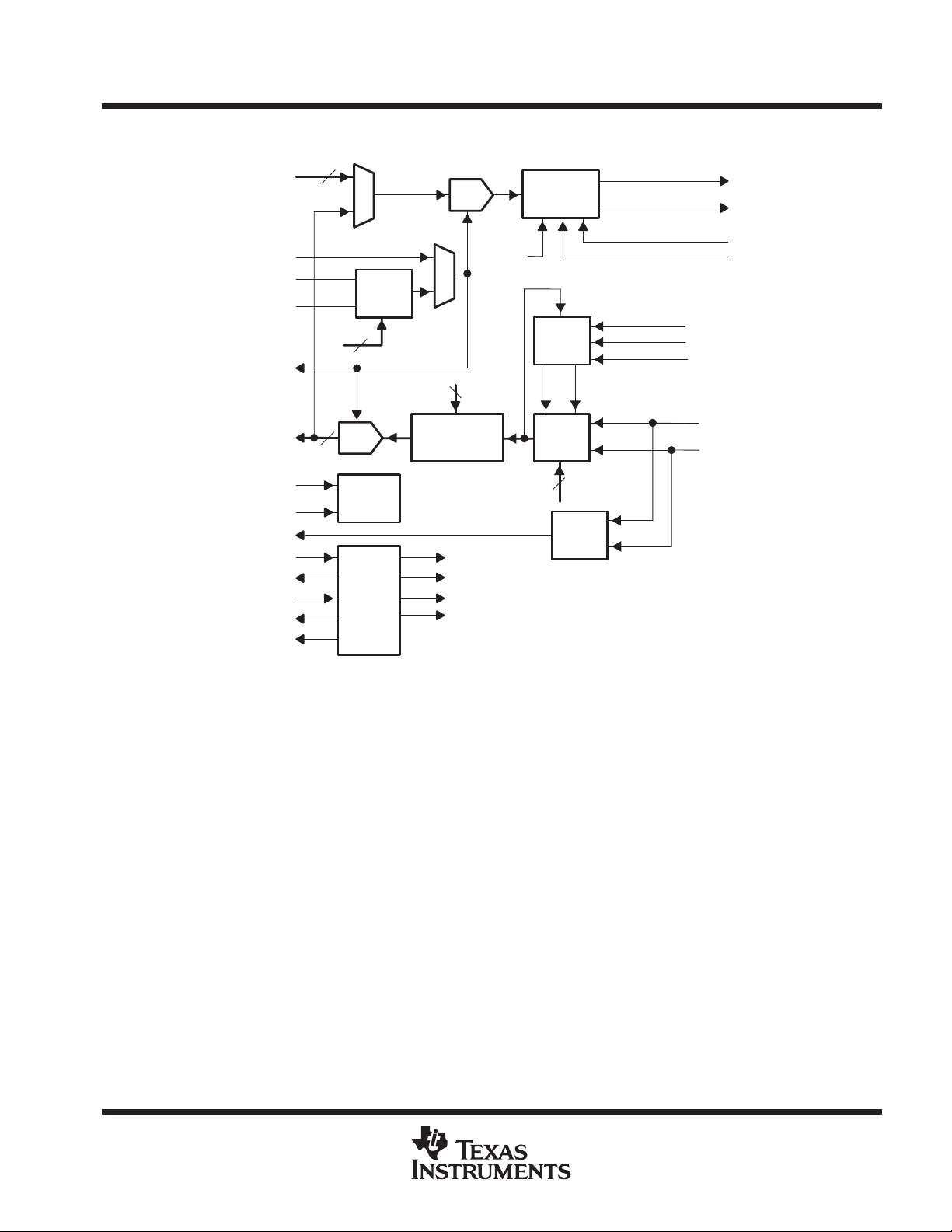
functional block diagram
TLV320VD30
VDSL CODEC
SLWS086 – JUNE 1999
DAC<11:0>
CLKIN
XIN
XOUT
CLKOUT
ADC<11:0>
TXENABLE
RXENABLE
TONEDETECT
SENABLE
SCLK
SIN
SOUT
SREADY
12
bits
bits
12
9
bits
ADC
Control
Control
NCXO
Power
Serial
BUS
DAC
TXPOWER
M
U
X
2
bits
Compromise
Equalizer
NCXO
TXPOWER
CEQ
PGA
3 bits
Line Driver
Interface
RFI
Cancel
I
PGA
5
bits
Tone
Detect
TXP
TXM
SENSETXP
SENSETXM
VCMSENSEM
VCMSENSEP
RFIADAPTEN
Q
RXP
RXM
POST OFFICE BOX 655303 • DALLAS, TEXAS 75265
3

TLV320VD30
I/O
DESCRIPTION
VDSL CODEC
SLWS086 – JUNE 1999
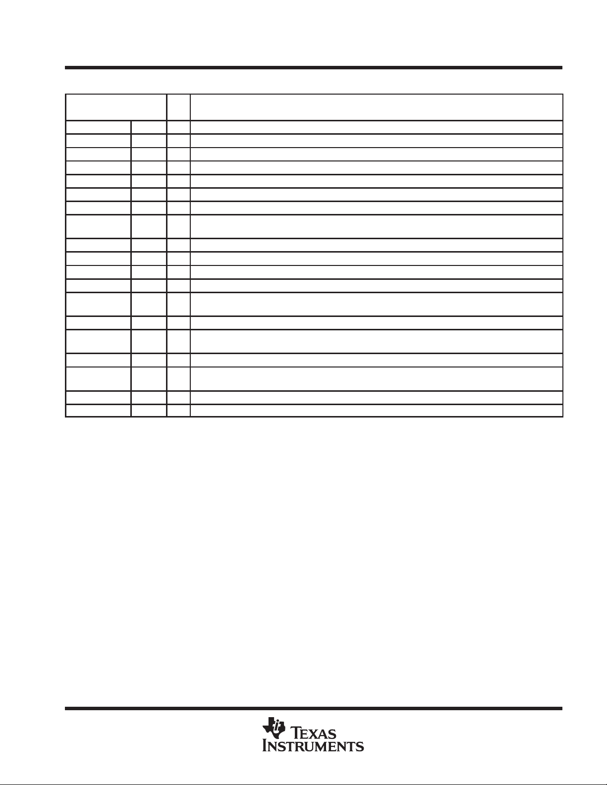
Terminal Functions
TERMINAL
NAME NO.
ADC<0,11> 15–26 O Digital receive data. Data format can be straight offset binary or 2s complement. Data output on falling
ADCGND 33 Analog ADC ground
ADCGNDREF 35 ADC ground reference
ADCVDD 32 Analog ADC VDD, 3.3 V
AGND1 37 Analog ground
AGND2 49 Analog ground
AGND3 56 Analog ground
AGND4 62 Analog ground
TESTM 43 I/O Reserved for test. No connection.
TESTP 41 I/O Reserved for test. No connection.
TESTCLK 38 I/O Reserved for test. No connection.
AVDD1 36 Analog VDD, 3.3 V
AVDD2 52 Analog VDD, 3.3 V
AVDD3 57 Analog VDD, 3.3 V
AVDD4 63 Analog VDD, 3.3 V
CLK 10 O System clock, 22.08 MHz
CLKIN 66 I External clock input
DAC<11:0> 77,78,
79,80,
1–8
DGND 76 Digital ground
DGNDIO 11 Digital I/O ground
DGNDIO 28 Digital I/O ground
DVDD 75 Digital VDD, 3.3 V
DVDDIO 9 Digital I/O VDD, 2.5 V/3.3 V
DVDDIO 27 Digital I/O VDD, 2.5 V/3.3 V
EXTCLKEN 67 I External Clock Enable
GAURDGND 31 Isolation ground.
GUARDGND 59 Isolation ground
GUARDVDD 30 Isolation VDD, 3.3 V
GUARDVDD 58 Isolation V
NC 34 No connection
RESET 68 I Device reset
RFIADAPTEN 70 I RFI cancellation adapt enable
RSET 60 I/O Resistor current set requires an external 621 Ω, 1% resistor
RXM 50 I Receiver input (–)
RXP 51 I Receiver input (+)
RXENABLE 72 I Receive enable (active high). RXENABLE signal provides a minimum of 5 µs warning of an impending
TEST3 69 I Reserved for test. No connection.
SCLK 13 O Serial bus clock (frequency = CLK/16 or 1.38 MHz)
SENABLE 73 I Serial bus enable (active high). SENABLE high indicates that the DSP interface is requesting activation of
edge of clock.
I Digital transmit data. Data format can be straight offset binary or 2s complement. Data input on rising edge
of clock.
DD
receive burst. This signal remains High until the DMT engine has received the last ADC data word.
the serial input.
4
POST OFFICE BOX 655303 • DALLAS, TEXAS 75265
I/O
DESCRIPTION
TLV320VD30
VDSL CODEC
SLWS086 – JUNE 1999
Terminal Functions (Continued)
TERMINAL
NAME NO.
SENSETXM 46 I/O Transmitter current sense(–). Connects to external line driver.
SENSETXP 55 I/O Transmitter current sense(+). Connects to external line driver.
SIN 74 I Serial bus input
SOUT 12 O Serial bus output. SOUT is high impedance when SENABLE is low.
SREADY 14 O SREADY indicates when the device is ready to output serial data.
TDVREFM 45 I/O T one detector reference V(–). Connects to an external resistor divider.
TDVREFP 44 I/O T one detector reference V(+). Connects to an external resistor divider
TONEDETECT 29 O Wake-up tone detector output. Remains low when the tone detector is disabled. When the tone detector is
TXM 47 I/O Transmitter output (–). Connects to external line driver.
TXP 54 I/O Transmitter output (+). Connects to external line driver.
TXBIASM 48 I/O Transmitter bias current (–). Connects to external line driver.
TXBIASP 53 I/O Transmitter bias current (+). Connects to external line driver.
TXENABLE 71 I Transmitter enable (active high). TXENABLE signal provides up to 5 µs of warning of an impending transmit
VBG 61 I/O Voltage bandgap reference, 1.25 V. Requires an external 0.1 µF capacitor.
VCM 42 I/O Common mode voltage reference. Connects to an internally generated 1.5 V reference, requires an external
VCMSENSEM 40 I/O Reference for VCMSENSEM
VCMSENSEP 39 I/O Transformer common mode input signal used by the RFI canceller . Connects to transformer line-side center
XIN 64 I/O 22.08 MHz crystal input
XOUT 65 I/O 22.08 MHz crystal output
enabled, goes high when a wake-up tone is present.
burst. This signal remains High until the last TX data word has been registered.
0.1 µF bypass capacitor.
tap through an external attenuator.
absolute maximum ratings over operating free-air temperature (unless otherwise noted)
†
Supply voltage, AVDD, DVDD, DVDDIO –0.5 V to 4 V. . . . . . . . . . . . . . . . . . . . . . . . . . . . . . . . . . . . . . . . . . . . . .
Analog input voltage range –0.5 V to AVDD+0.5 V. . . . . . . . . . . . . . . . . . . . . . . . . . . . . . . . . . . . . . . . . . . . . . . . . .
Digital input voltage range –0.5 V to DVDD+0.5 V. . . . . . . . . . . . . . . . . . . . . . . . . . . . . . . . . . . . . . . . . . . . . . . . . .
Operating
Operating
Storage temperature range, T
virtual junction temperature range, T
free-air temperature range, T
–65°C to 150°C. . . . . . . . . . . . . . . . . . . . . . . . . . . . . . . . . . . . . . . . . . . . . . . . . . .
str
–40°C to 85°C. . . . . . . . . . . . . . . . . . . . . . . . . . . . . . . . . . . . . . . . . . . . .
A
–40°C to 150°C. . . . . . . . . . . . . . . . . . . . . . . . . . . . . . . . . . . . .
J
Lead temperature 1,6 mm (1/16 inch) from case for 10 seconds 260°C. . . . . . . . . . . . . . . . . . . . . . . . . . . . . . .
†
Stresses beyond those listed under “absolute maximum ratings” may cause permanent damage to the device. These are stress ratings only, and
functional operation of the device at these or any other conditions beyond those indicated under “recommended operating conditions” is not
implied. Exposure to absolute-maximum-rated conditions for extended periods may affect device reliability.
POST OFFICE BOX 655303 • DALLAS, TEXAS 75265
5
TLV320VD30
Power dissipation
mW
High-level input voltage, V
V
Low-level input voltage, V
V
High-level input current, I
A
Low-level input current, I
A
High-level output voltage, V
V
Low-level output voltage, V
V
High-level output current, I
mA
Low-level output current, I
mA
VDSL CODEC
SLWS086 – JUNE 1999
recommended operating conditions
power supply
MIN NOM MAX UNIT
AVDD 3 3.3 3.6
Supply voltage
p
PSRR (see Note 2) Frequency = 150 kHz –45 dB
NOTES: 1. Does not include line driver.
2. PSRR measurement are made with the TX and RX channels idle and a 400 mVpp signal.
digital inputs/outputs
p
p
p
p
p
p
p
p
DVDD 3 3.3 3.6
DVDDIO 2.5/3.3
TX active (see Note 1) 110 200
RX active 500 700
RX standby mode 100
Power-down mode, TX/RX disabled 60
MIN NOM MAX UNIT
DVDD, DVDDIO = 3.3 V 2.4
IH
DVDD = 3.3 V, DVDDIO = 2.5 V 2
IL
IH
iL
DVDD, DVDDIO = 3.3 V 0.6
DVDD = 3.3 V, DVDDIO = 2.5 V 0.6
DVDD, DVDDIO = 3.3 V 100
DVDD = 3.3 V, DVDDIO = 2.5 V 100
DVDD, DVDDIO = 3.3 V 100
DVDD = 3.3 V, DVDDIO = 2.5 V 100
DVDD, DVDDIO = 3.3 V 2.4
OH
DVDD = 3.3 V, DVDDIO = 2.5 V 2
DVDD, DVDDIO = 3.3 V 0.6
OL
DVDD = 3.3 V, DVDDIO = 2.5 V 0.6
DVDD, DVDDIO = 3.3 V 1
OH
DVDD = 3.3 V, DVDDIO = 2.5 V 1
DVDD, DVDDIO = 3.3 V 1
OL
DVDD = 3.3 V, DVDDIO = 2.5 V 1
V
µ
µ
clock inputs
Input clock frequency 22.08 MHz
Input clock duty cycle 45% 50% 55%
reference voltage
VCM (common mode) AVDD = 3.3 V 1.4 1.6 V
VBG (band gap) AVDD = 3.3 V 1.20 1.25 1.30 V
NCXO
Step size AVDD = 3.3 V 1 ppm
Range AVDD = 3.3 V 200 250 ppm
6
MIN NOM MAX UNIT
MIN NOM MAX UNIT
MIN NOM MAX UNIT
POST OFFICE BOX 655303 • DALLAS, TEXAS 75265
TLV320VD30
VDSL CODEC
SLWS086 – JUNE 1999
electrical characteristics over recommended operating free-air temperature range, TA = 255C,
AVDD = 3.3 V, DVDD = 3.3 V, f
CLKIN
TXDAC
PARAMETER TEST CONDITIONS MIN TYP MAX UNIT
Signal bandwidth 43k 11.04M Hz
Conversion rate 22.08 MHz
AC Performance
Single tone
Transmit 2nd harmonic 1.4 MHz at –3 dbfs –77 –60 –55 dB
Transmit 3rd harmonic 1.4 MHz at –3 dbfs –75 –67 –67 dB
THD 1.4 MHz at –3 dbfs –64 –58 –54 dB
SNR 1.4 MHz at –3 dbfs –56 –55 –54 dB
SNDR (see Note 3) 1.4 MHz at 0 dbfs –46 –45 –44 dB
Channel delay 90 150 nS
NOTE 3: Signal-to-noise and distortion
= 22.08 MHz (unless otherwise noted)
1.4 MHz at –3 dbfs –54 –53 –51 dB
1.4 MHz at –6 dbfs –51 –50 –49 dB
1.4 MHz at –12 dbfs –42 –41 –40 dB
1.4 MHz at –18 dbfs –31 –30 –29 dB
1.4 MHz at –24 dbfs –22 –20 –21 dB
1.4 MHz at –30 dbfs –10 –9 –8 dB
POST OFFICE BOX 655303 • DALLAS, TEXAS 75265
7

TLV320VD30
SNDR (see Note 3)
Missing tone test
Compromise equalizer
VDSL CODEC
SLWS086 – JUNE 1999
electrical characteristics over recommended operating free-air temperature range, TA = 255C,
AVDD = 3.3 V, DVDD = 3.3 V, f
CLKIN
RXADC channel characteristics
PARAMETER TEST CONDITIONS MIN TYP MAX UNIT
Signal bandwidth 43k 11.04M Hz
Conversion rate 22.08 MHz
CMRR –50 –44 –37 dB
PGA gain error 1 dB
AC Performance
Single tone
Transmit 2nd harmonic 1.4 MHz at –3 dbfs –68 –66 –64 dB
Transmit 3rd harmonic 1.4 MHz at –3 dbfs –66 –65 –63 dB
THD 1.4 MHz at –3 dbfs –64 –62 –61 dB
SNR 1.4 MHz at –3 dbfs –59 –58 –57 dB
p
Channel delay 150 200 nS
NOTE 3: Signal-to-noise and distortion
= 22.08 MHz (unless otherwise noted) (continued)
1.4 MHz at 0 dbfs –59 –58 –57 dB
1.4 MHz at –3 dbfs –58 –57 –56 dB
1.4 MHz at –6 dbfs –52 –51 –50 dB
1.4 MHz at –12 dbfs –40 –39 –38 dB
1.4 MHz at –18 dbfs –28 –25 –24 dB
1.4 MHz at –24 dbfs –21 –18 –13 dB
RX total deviation 2.38 2.42 2.45 dB
RX missing tone 2.72 MHz –60 –48 –44 dB
RX missing tone 5.52 MHz –53 –47 –43 dB
RX missing tone 8.28 MHz –65 –54 –50 dB
RX CEQ-00 MAG at 4 MHz –37 –36 dB
RX CEQ-01 MAG at 4 MHz –36 –34.5 dB
RX CEQ-10 MAG at 4 MHz –34 –33 dB
RX CEQ-11 MAG at 4 MHz –32.5 –31 dB
RFI cancellation
At 4 MHz –45 –20 dB
At 8 MHz –45 –25 dB
receiver (RX+, RX–)
Voltage range AVDD = 3.3 V, VCM ~1.5 V VCM±2 V
Input current AVDD = 3.3 V 10 mA
8
PARAMETER TEST CONDITIONS MIN TYP MAX UNIT
PARAMETER TEST CONDITIONS MIN TYP MAX UNIT
POST OFFICE BOX 655303 • DALLAS, TEXAS 75265

TLV320VD30
VDSL CODEC
SLWS086 – JUNE 1999
detailed description
device functions
The following sections describe the functions of the device.
transmit block
Transmit block contains the DAC and a special class AB line-driver interface that connects to external bipolar
transistors and the center-tapped transformer to obtain peak output current of 200 mA, peak voltage of 1 1 Vpp
differential with a 110 Ω load. This circuit has been specially designed to deliver average power of 11 dBm
(11 mW) to a 110 W reference impedance twisted-pair line with good linearity and low power consumption in
a single bandwidth up to 11 MHz. Additionally the power level can be adjusted downward in 4 steps of 6 dB.
To conserve power, this block is only enabled when the device is in the transmit mode. It is activated when the
external TXENABLE signal is registered by the control logic. When this occurs, the control logic simultaneously
generates a TXRESET signal that remains asserted for approximately 5 µs after TXENABLE is asserted. The
TXRESET signal causes the transmitter to force 25 mV across the two external sense resistors, defining the
Vout = 0 state. When TXRESET is released, the transmit output follows the input data until the TXENABLE signal
is released, at which time the transmitter is powered down.
The transmitter output power level can be adjusted between –13 and 1 1 dBm (into 110 Ω) in increments of 6 dB.
This is accomplished by programming bits 5:3 of mode control register (register 3). The digital format of the
TX<1 1:0> input data can either be straight of fset binary or 2s complement, as determined by the MSBINV bit,
bit 1 of mode control register (register 3).
The transmit path of the AFE utilizes a class AB current output configuration. Because of the class AB operation,
the output signal must be generated by two separate channels—one channel which generates positive values
of the transmit signal and the other channel responsible for negative values. Each channel consists of an 11
bit DAC and a TxAmp, which provides the base current for the external bipolar output devices. Given a 12 bit
digital input in straight offset binary format (i.e., midscale = 1000 0000 0000 = 0 V differential), the MSB of the
input data determines which DAC is activated for a given code. The remaining 1 1 bits control the collector current
level in the activated channel, which results in 12 bits of programmability.
Each 1 1 bit DAC has 2048 programmable output levels. To maintain symmetry , an input code of 0 results in an
output of step of 1/2 LSB. When the transmitter output is evaluated differentially , this results in a 1 LSB transition
when crossing the midpoint of the transfer function (i.e., when switching from one DAC to the other). The
following table identifies some of the critical input codes and their corresponding output values:
Table 1. Input Codes and Output Values
TX<11:0> RsenseP RsenseM RsenseP – RsenseM
1111 1111 1111 (4095) Vidle + 2047 1/2 LSBs Vidle 2047 1/2 LSBs
1111 1111 1110 (4094) Vidle + 2046 1/2 LSBs Vidle 2046 1/2 LSBs
1000 0000 0001 (2049) Vidle + 1 1/2 LSBs Vidle 1 1/2 LSBs
1000 0000 0000 (2048) Vidle + 1/2 LSBs Vidle 1/2 LSBs
0111 1111 1111 (2047) Vidle Vidle + 1/2 LSBs –1/2 LSBs
0111 1111 1110 (2046) Vidle Vidle + 1 1/2 LSBs –1 1/2 LSBs
0000 0000 0001 (1) Vidle Vidle + 2046 1/2 LSBs –2046 1/2 LSBs
0000 0000 0000 (0) Vidle Vidle + 2047 1/2 LSBs –2047 1/2 LSBs
External low pass filtering is needed for noise reduction. A minimum requirement is a fourth order Butterworth
low pass filter with cutoff frequency between 11 MHz and 12 MHz.
POST OFFICE BOX 655303 • DALLAS, TEXAS 75265
9

TLV320VD30
VDSL CODEC
SLWS086 – JUNE 1999
detailed description (continued)
TXENABLE
CLKIN
Default
CLKOUT
5 µs
t
cc
t
cd
t
u
t
d
DAC<11:0>
RXENABLE
CLKIN
CLKOUT
ADC<11:0>
t
s
t
h
Figure 1. Timing Sequence of the DAC
t
cc
t
cd
5 µs
Default
t
u
t
d
t
1
10
Figure 2. Timing Sequence of the ADC
POST OFFICE BOX 655303 • DALLAS, TEXAS 75265

TLV320VD30
VDSL CODEC
SLWS086 – JUNE 1999
detailed description (continued)
Table 2. Clock Timing
MIN MAX UNITS
t
t
tone detector
In both VDSL transceiver unit-central office end (VTU-O) and VDSL transceiver unit-remote terminal
end(VTU-R) units, much of the analog system will be in power down mode unless it is in use. So, a special signal
is needed to indicate that a unit is requesting activation. The tone detector detects this special signal. Therefore
it is enabled only in the receive standby mode. During this time, the tone detector constantly monitors the
received signal for the presence of a wake up tone, The tone frequency can be either 172.5 kHz or 345 kHz (bins
4 and 8, respectively , where bin is the frequency plane that split up into blocks of frequencies of 43.125 kHz).
The wake up tone should be at least 225 µs duration. In the upstream direction, when a remote unit requests
activation, it will send a 172.5 kHz frequency sinusoid, corresponding to bin 4. In the absence of noise, the peak
amplitude of the received wake up tone can very from 7 mV for a long line to 100 mV for a short line. The choice
of tone frequency is determined by the TDBIN register bit, bit 0 of the mode control register (register 3), a logic
0 sets the frequency to 172.5 kHz (bin 4), and a logic 1 sets the frequency to 345 kHz (bin 8).
42 ns
cc
t
19 ns
u
t
19 ns
d
t
r
t
f
cd
t
t
t
0 ns
0 tu + tr – tcd – 5 ns
1
0 tcc – tcd – 20 ns
s
0 tcc – tcd – 4 ns
h
2 ns
2 ns
The tone detector block also has large clamp switches, which are closed when either the transmitter is enabled
or the receiver is being reset to keep the internal voltages within the supply rails when transmitting.
PGA/MDAC
The PGA/MDAC block is a low noise, low distortion amplifier that performs several functions. Primarily, The
PGA/MDAC is a variable gain amplifier that increases the strength of the receive signal from 0 dB to 20 dB in
increments of 1 dB. The gain is controlled using bits 4:0 of the RX control register (register 1). In addition, when
RFI cancellation is enabled, this block performs the weighting of the I and Q common mode signals and sums
them with the receive signal.
compromise equalizer
The compromise equalizer (CEQ) provides signal gain to the frequencies in the upper end of the signal band
to compensate for the high frequency attenuation in the line. Because of large processing tolerances, the corner
frequency has two bits of programmability. The compromise equalizer implements the following transfer
function:
H(f) = k (s + z)
2
÷ (s + p)
2
When selected, or when it is bypassed by register control, H(f) = 1. The compromise equalizer can be bypassed
by setting bit 7 of RX control register (register 1) to 1 and can be tuned by programming bits 5,6 of the same
register.
POST OFFICE BOX 655303 • DALLAS, TEXAS 75265
11

TLV320VD30
VDSL CODEC
SLWS086 – JUNE 1999
detailed description (continued)
RFI canceller
The RFI canceller block reduces the magnitude of RFI present in the received signal to the same power level
as the smallest desired signal. It is assumed that the interferer is related to the common mode signal present
on the line. An attenuated form of this common mode signal is used by the RFI canceller to generate differential
I and Q signals which are weighted and summed with the RX signal in the PGA block. The output of the PGA
is mixed with each of the I and Q signals in a correllator, whose output is used to drive a digital integrator (12
bit up/down counters) in the control block. The counter outputs determine the I/Q weighting coefficients that are
used by the PGA.
The RFI canceller adapts for 25 µs every 475 µs during quiet frames after receiving. When the line is in use,
the coefficients are held constant, as shown in Figure 3.
Superframe Period = 500 µs
RX Quiet
Update Enable
25 µs
TX
Quiet RX
Quiet
Update Enable
25 µs
Figure 3. A VDSL Super Frame
ADC
The ADC block uses a pipeline architecture to convert the analog Rx signal into 12 bit digital data. The analog
input is first converted into discrete time data by the sample and hold. A 5-bit flash ADC then quantizes the signal
to 5 bits, which provides the 5 MSBs of the final 12-bit word. These 5 bits are also used to drive a 5-bit DAC;
the output is subtracted from the original input signal. The residual voltage is then amplified by the first subrange
amplifier, and the resulting signal is used to perform another analog-to-digital-to-analog conversion to obtain
the middle 5 bits of the final 12-bit word. The process is repeated one final time in the third ADC, which is only
4 bits.
NCXO
The numerically controlled oscillator (NCXO) block is responsible for controlling the system clock used by both
the AFE and the DMT engine. When the external EXTCLKEN terminal is LOW and a 22.08 MHz crystal is
connected between the XIN and XOUT terminals, the system clock is generated internally and has 9 bits of
tuning resolution, with approximately 1 ppm of resolution per bit. When EXTCLKEN is HI, the NCXO block is
powered down and an external clock source (CLKIN) is used as the system clock.
POR
In the absence of an external reset signal, the POR block is responsible for generating an internal reset signal
when the chip is initially powered. It functions in conjunction with its I/O pad cell, which is responsible for level
shifting the external logic level (which could be 2.5 V) up to the internal core voltage of 3.3 V nominal. Reset
interval is 25 µs.
bandgap
The bandgap block generates a nominal 1.25-V reference voltage that is relatively insensitive to variations in
temperature, supply voltage, and processing.
12
POST OFFICE BOX 655303 • DALLAS, TEXAS 75265

TLV320VD30
VDSL CODEC
SLWS086 – JUNE 1999
control logic
power mode description
The control logic is responsible for controlling all of the possible power modes available on the ASIC. External
control of the power mode can be achieved through either a combination of the external TXENABLE and
RXENABLE input terminals or through the power mode register bit accessible via the serial interface.
external power control
When the power mode register bit (Reg7<0>) is set high, control of the operational power mode is achieved
through the external TXENABLE and RXENABLE input terminals as described in Figure 4.
POR/
External RESET
11
nn = TXENABLE, RXENABLE
00
TX Quiet
0x x0
TX Reset
TX
RX Standby
11 11
10
Timer
RX Quiet
01
RX Reset
Timer
RX
Figure 4. State Diagram for External Power Mode Control
By defining separate states for TX Quiet and RX Quiet, it is possible to adapt the RFI canceller during the RX
Quiet state without having to power up the RFI canceller during the TX Quiet state. The remaining modes are
defined in Table 3.
Table 3. Power Modes
UNIT TRANSMIT RECEIVE RxSTANDBY TEST
DAC X X
Line driver X X
RFI canceller X X X
Tone detector X X
PGA X X
ADC X X
CEQ X X
NCXO X X X X
Serial bus X X X X
POST OFFICE BOX 655303 • DALLAS, TEXAS 75265
13

TLV320VD30
VDSL CODEC
SLWS086 – JUNE 1999
serial bus power control
When the power mode register bit (Reg7<0>) is set low, control of the each of the following major functional
blocks is obtained through their individual enable register bits in Register 7.
D
RFI canceller
D
PGA
D
CEQ
D
ADC
D
Transmitter
D
Tone detector
serial interface operation
A serial interface has been included to allow both read and write access of the 7 internal 12-bit registers. The
serial clock (SCLK) is generated internally and operates at 1.38 MHz (22.08 MHz system clock divided by 16).
Data is transferred across the interface in groups of 16 bits each, the order of which is as shown in Table 4,
(lsb first):
Table 4. Data Transfer Order
SerBit<0> SerBit<1> SerBit<2> SerBit<3> SerBit<4> SerBit<5> … SerBit <15>
R/W (Read = 1, Write = 0) Reg<0> Reg<1> Reg<2> Data<0> Data<1> … Data<11>
A read or write operation is initiated when the SENABLE input terminal is sampled high on the rising edge of
SCLK. The incoming data is then captured over the following 16 rising edges of SCLK. The first bit determines
whether a read or write is to take place (read = 1, write = 0). The next 3 bits determine the address of the register
to be accessed. If a write operation is chosen, the remaining 12 bits of SIN data represent the data to be written
to the addressed register, thus completing the write operation. This is shown in Figure 5.
SCLK
SENABLE
SIN
Figure 5. Register Write Operation Timing Diagram
If a read operation has been selected, these 12 data bits are ignored. For a read operation, the SREADY output
terminal is asserted for one clock cycle immediately following the clocking of SerBit<15> followed by 16 bits of
data on the SOUT output terminal in the order outlined above. SerData<0> is always 1 in this case for
the Reg<2:0> field indicates the data register being read. This is shown in Figure 6.
01 23 4 131415
read
, and
14
POST OFFICE BOX 655303 • DALLAS, TEXAS 75265

serial interface operation (continued)
SCLK
SREADY
TLV320VD30
VDSL CODEC
SLWS086 – JUNE 1999
SOUT
0 1 2 3 4 11 12 13 14 15
Figure 6. Register Read Operation Timing Diagram
register map
REGISTER/
BIT
0 ****************************** NOT USED ******************************
Default ****************************** NOT USED ******************************
1 RSTTIME<3:0> CeqBP CEQ<1:0> PGA Gain <4:0> (Default = 20 dB)
Default 1 1 0 1 1 0 0 1 0 1 0 0
2 NCXO<8:0>
Default 1 0 0 0 0 0 0 0 0 0 0 0
3 TxPower <2:0>
Default 0 0 0 0 0 0 0 0 0 0 0 0
4 Reserve for Test Up/Dn Up/Dn Cntl Up./Dn Inv RFIstep<1:0> RFIon line
Default 0 0 0 0 0 0 0 0 0 0 0 0
5 Icoeff<11:0>
Default 1 0 0 0 0 0 0 0 0 0 0 0
6 Qcoeff<1 1:0>
Default 1 0 0 0 0 0 0 0 0 0 0 0
7 RSTDEF
Default 1 1 1 1 1 1 1 1 1 1 1 1
11 10 9 8 7 6 5 4 3 2 1 0
Reserved for
T est
TD
Enable
ADC
Enable
Ceq
Enable
PGA
Enable
Loop
Back
RFI
EnableTXEnable
MSB INV TDBIN
Power Mode
POST OFFICE BOX 655303 • DALLAS, TEXAS 75265
15

TLV320VD30
VDSL CODEC
SLWS086 – JUNE 1999
detail of the internal registers
Name: Rx Control Register Address: 1 No. of Bits: 12
BITS ACCESS NAME DESCRIPTION
11:8 RW RSTTIME When the reset counter is in register control mode (RSTDEF = 0), these bits are used to control the
7 RW CEQBP Controls the operational mode of the CEQ:
6:5 RW CEQ<1:0> Controls the tuning of the CEQ output spectrum:
4:0 RW PGAGAIN Controls the gain of the PGA
duration of the RESET counter. The reset duration can be calculated using
t
The default value of RSTTIME = 1101 (13d), which results in a 5.068 µs delay.
= [dec(RSTTIME<3:0>) + 1] × 362 ns.
reset
0: CEQ spectrum shaping enabled
1: Bypass [flat frequency response] (default)
00: Max gain at 4 MHz (default)
01:
10:
11: Min gain at 4 MHz
00000: 0 dB
00001: 1 dB
00010: 2 dB
•
•
10010: 18 dB
1001 1: 19 dB
10100: 20 dB (default)
10101: 0 dB
•
•
11111: 0 dB
Name: NCXO Control Register Address: 2 No. of Bits: 12
BITS ACCESS NAME DESCRIPTION
11:3 RW NCXO Controls the tuning of the NCXO:
2:0 RW Reserved
0 0000 0000: Max. CLK frequency
1 0000 0000: Nominal CLK frequency (default)
1 1111 1111: Min. CLK frequency
Name: Mode Control Register Address: 3 No. of Bits: 12
BITS ACCESS NAME DESCRIPTION
11:6 RW Reserved
5:3 RW TXPOWER These bits select the output power level of the transmitter:
2 RW LOOPBACK In test mode, determines whether digital loopback is enabled:
1 RW MSBINV This bit determines the digital format of the Tx/Rx digital data:
0 RW TDBIN This bit selects the wake up tone frequency:
000: 11 dBm (default)
001: 5 dBm
010: –1 dBm
011: –7 dBm
1xx: –13 dBm
0: Loopback disabled (default)
1: Loopback enabled
0: Straight offset binary (default)
1: 2s complement
0: Bin 4 [172.5 kHz] (default)
1: Bin 8 [345 kHz]
16
POST OFFICE BOX 655303 • DALLAS, TEXAS 75265

detail of the internal registers (continued)
Name: RFI Cntrl/Test Register Address: 4 No. of Bits: 12
BITS ACCESS NAME DESCRIPTION
11.6 RW Reserved Reserved for test
5 RW Up/down When up/down Cntl is high, this bit selects the direction of the 12 bit I/Q counters:
0: Down (default)
1: Up
4 RW Up/down Cntl When in test mode, this bit controls the source of 12 bit I/Q counter control:
0: Correlator output (default)
1: Up/down register bit
3 RW Up/down Inv Controls whether the 12 bit I/Q counter inputs are inverted:
0: No inversion (default)
1: Counter inputs inverted.
2:1 RW RFIstep Controls adaptation rate of the I/Q coefficients:
00 = COUNT<11:4> (default)
01 = COUNT<10:3>
10 = COUNT<9:2>
11 = COUNT<8:1>
0 RW RFIonline Disables RFI canceller:
0: RFI canceller disabled (default)
1: RFI canceller enabled
TLV320VD30
VDSL CODEC
SLWS086 – JUNE 1999
Name: I Coefficients Register Address: 5 No. of Bits: 12
BITS ACCESS NAME DESCRIPTION
11:0 RW Icoeff Controls the weighting of the I common mode component summed with the Rx signal.
Name: Q Coefficients Register Address: 6 No. of Bits: 12
BITS ACCESS NAME DESCRIPTION
11:0 RW Qcoeff Controls the weighting of the Q common mode component summed with the Rx signal.
POST OFFICE BOX 655303 • DALLAS, TEXAS 75265
17

TLV320VD30
VDSL CODEC
SLWS086 – JUNE 1999
detail of the internal registers (continued)
Name: Power Modes Register Address: 6 No. of Bits: 12
BITS ACCESS NAME DESCRIPTION
11.10 RW Reserved
9:7 RW RSTDEF Determines source of RESET counter coef ficients:
0: TSTTIME<3:0>
1: Hard-wired value (default)
8:7 RW Reserved Reserved for test
6 RW TD Enable Enables/disables tone detector in power mode:
0: Disabled
1: Enabled (default)
5 RW ADC Enable Enables/disables ADC in power mode:
0: Disabled
1: Enabled (default)
4 RW CEQ Enable Enables/disables CEQ in power mode:
0: Disabled
1: Enabled (default)
3 RW PGA Enable Enables/disables PGA in power mode:
0: Disabled
1: Enabled (default)
2 RW RFI Enable Enables/disables RFI canceller in power mode:
0: Disabled
1: Enabled (default)
1 RW TX Enable Enables/disables transmitter in power mode:
0: Disabled
1: Enabled (default)
0 RW POWERMODE Determine source of power mode control:
0: Power mode control registers
1: External RXEN and TXEN (default)
18
POST OFFICE BOX 655303 • DALLAS, TEXAS 75265

TLV320VD30
VDSL CODEC
SLWS086 – JUNE 1999
APPLICATION INFORMATION
The high throughput VDSL can be easily made compatible with SONET and A TM-based services. VDSL can
be used in a business or campus environment for providing high-speed digital transmission connections.
Similarly , a VDSL system can be used to interconnect users within any concentrated area for high speed intranet
use.
Figure 7 gives a block level system representation. This system is capable of providing up to 52 Mb/s over
unshielded twisted pair at ranges of 300–1500m.
Data
Interface
(DI)
DMT
Engine
DSPRAM
Analog
Front
End
Figure 7. System Block Diagram
Transformer
Filter
Line
POST OFFICE BOX 655303 • DALLAS, TEXAS 75265
19

TLV320VD30
VDSL CODEC
SLWS086 – JUNE 1999
MECHANICAL DATA
PN (S-PQFP-G80) PLASTIC QUAD FLATPACK
80
61
1,45
1,35
0,50
60
1
9,50 TYP
12,20
SQ
11,80
14,20
SQ
13,80
0,27
0,17
20
41
0,08
M
40
21
0,05 MIN
0,13 NOM
Gage Plane
0,25
0°–7°
0,75
0,45
1,60 MAX
NOTES: A. All linear dimensions are in millimeters.
20
B. This drawing is subject to change without notice.
C. Falls within JEDEC MS-026
POST OFFICE BOX 655303 • DALLAS, TEXAS 75265
Seating Plane
0,08
4040135 /B 11/96

IMPORTANT NOTICE
T exas Instruments and its subsidiaries (TI) reserve the right to make changes to their products or to discontinue
any product or service without notice, and advise customers to obtain the latest version of relevant information
to verify, before placing orders, that information being relied on is current and complete. All products are sold
subject to the terms and conditions of sale supplied at the time of order acknowledgement, including those
pertaining to warranty, patent infringement, and limitation of liability.
TI warrants performance of its semiconductor products to the specifications applicable at the time of sale in
accordance with TI’s standard warranty. Testing and other quality control techniques are utilized to the extent
TI deems necessary to support this warranty . Specific testing of all parameters of each device is not necessarily
performed, except those mandated by government requirements.
CERT AIN APPLICATIONS USING SEMICONDUCTOR PRODUCTS MAY INVOLVE POTENTIAL RISKS OF
DEATH, PERSONAL INJURY, OR SEVERE PROPERTY OR ENVIRONMENTAL DAMAGE (“CRITICAL
APPLICATIONS”). TI SEMICONDUCTOR PRODUCTS ARE NOT DESIGNED, AUTHORIZED, OR
WARRANTED TO BE SUITABLE FOR USE IN LIFE-SUPPORT DEVICES OR SYSTEMS OR OTHER
CRITICAL APPLICA TIONS. INCLUSION OF TI PRODUCTS IN SUCH APPLICATIONS IS UNDERST OOD TO
BE FULLY AT THE CUSTOMER’S RISK.
In order to minimize risks associated with the customer’s applications, adequate design and operating
safeguards must be provided by the customer to minimize inherent or procedural hazards.
TI assumes no liability for applications assistance or customer product design. TI does not warrant or represent
that any license, either express or implied, is granted under any patent right, copyright, mask work right, or other
intellectual property right of TI covering or relating to any combination, machine, or process in which such
semiconductor products or services might be or are used. TI’s publication of information regarding any third
party’s products or services does not constitute TI’s approval, warranty or endorsement thereof.
Copyright 1999, Texas Instruments Incorporated
 Loading...